em78p911a - emc.com.t · 2005/12/19 em78p911a 8-bit micro-controller elan microelectronics corp....
TRANSCRIPT
2005/12/19
EM78P911A
8-BIT MICRO-CONTROLLER
ELAN MICROELECTRONICS CORP. No. 12, Innovation 1st RD., Science-Based Industrial Park Hsin Chu City, Taiwan TEL: (03) 5639977 FAX: (03)5630118 (SA2)
Version 2.1
EM78P911A8-bit Micro-controller
__________________________________________________________________________________________________________________________________________________________________
* This specification is subject to change without notice. ~ ~ 1 12/19/2005 (V2.1)
Version history Date Version number Description Note 2005/12/19 2.1 Add DTMF detail description in page 33

EM78P911A8-bit Micro-controller
__________________________________________________________________________________________________________________________________________________________________
* This specification is subject to change without notice. ~ ~ 2 12/19/2005 (V2.1)
I.General Description The EM78P911A is an 8-bit CID (Call Identification) RISC type microprocessor with low power, high speed CMOS technology. Integrated onto a single chip are on_chip watchdog (WDT), RAM, ROM, programmable real time clock /counter, internal interrupt, power down mode, LCD driver, FSK decoder, CALL WAITING decoder, SDT decoder, DTMF generator, MEI(Multiple Extension Internetworking) and RTF(Request To Flash) functions, and tri-state I/O . The EM78P911A provides a single chip solution to design a CID of calling message_display. II.Feature CPU ‧Operating voltage range : 2.5V~5.5V ‧16K×13 on chip Electrical One Time Programmable Read Only Memory (OTP-ROM) ‧2.8K×8 on chip RAM ‧Up to 36 bi-directional tri-state I/O ports ‧8 level stack for subroutine nesting ‧8-bit real time clock/counter (TCC) ‧Two sets of 8 bit counters can be interrupt sources ‧Selective signal sources and trigger edges , and with overflow interrupt ‧Programmable free running on chip watchdog timer ‧99.9% single instruction cycle commands ‧Four modes (internal clock 3.579MHz)
1. Sleep mode : CPU and 3.579MHz clock turn off, 32.768KHz clock turn off 2. Idle mode : CPU and 3.579MHz clock turn off, 32.768KHz clock turn on
3. Green mode : 3.579MHz clock turn off, CPU and 32.768KHz clock turn on 4. Normal mode : 3.579MHz clock turn on , CPU and 32.768KHz clock turn on ‧Ring on voltage detector ‧ Universal Low battery detector ‧Input port wake up function ‧9 interrupt source , 4 external , 5 internal ‧100 pin QFP or chip ‧Port key scan function ‧Clock frequency 32.768KHz ‧Eight R-option pins CID ‧Operation Volltage 3.5 ~6V for FSK ‧Operation Volltage 2.5 ~6V for DTMF ‧Bell 202 , V.23 FSK demodulator ‧DTMF generator ‧Ring detector on chip CALL WAITING ‧Operation Volltage 3.6 ~5.5V ‧Compatible with Bellcore special report SR-TSV-002476 ‧ Call-Waiting (2130Hz plus 2750Hz) Alert Signal Detector ‧Good talkdown and talkoff performance ‧ Sensitivity compensated by adjusting input OP gain ‧ Minimum access frequency deviation ± 0.5% for U.S. Call waiting spec. (EM78P911A) SDT ‧ Stuttered Dial Tone (350Hz plus 440Hz) Signal Detect MEI/RTF ‧Compatible with TIA/EIA-777(TIA SP-4078) ‧MEI(Multiplex Extension Internetworking) and RTF(Request To Flash) functions

EM78P911A8-bit Micro-controller
__________________________________________________________________________________________________________________________________________________________________
* This specification is subject to change without notice. ~ ~ 3 12/19/2005 (V2.1)
LCD ‧LCD operation voltage chosen by software ‧Common driver pins : 16 ‧Segment driver pins : 60 ‧1/4 bias ‧1/8,1/16 duty PACKAGE ‧100 pin QFP (EM78P911AAQ, POVD disable) (EM78P911ABQ, POVD enable),
100 pin Chip or 102 pin Chip (with MEI and RTF functions) III.Application 1. adjunct units 2. answering machines 3. feature phones IV.Pin Configuration
EM78P911AAQ, EM78P911ABQ
Fig.1a Pin assignment
AV
SSD
TMF
PLLC
RIN
GTI
ME
RD
ET1
RIN
GTI
PG
AIN
CW
TIP
XIN
XO
UT
AV
DD
CO
M7
CO
M6
CO
M5
CO
M4
CO
M3
CO
M2
CO
M1
CO
M0
SEG
0SE
G1
SEG
2SE
G3
SEG
4SE
G5
SEG
6SE
G7
SEG
8SE
G9
SEG29SEG28SEG27SEG26SEG25SEG24SEG23SEG22SEG21SEG20SEG19SEG18SEG17SEG16SEG15SEG14SEG13SEG12SEG11SEG10
SEG30
SEG31
SEG32
SEG33
SEG34
SEG35
SEG36
SEG37
SEG38
SEG39
VSS
TESTC
OM
8/P60C
OM
9/P61C
OM
10/P62C
OM
11/P63C
OM
12/P64C
OM
13/P65C
OM
14/P66C
OM
15/P67SEG
40/P54SEG
41/P55SEG
42/P56SEG
43/P57SEG
44/P80SEG
45/P81SEG
46/P82SEG
47/P83SEG
48/P84SEG
49/P85SEG50/P86SEG51/P87SEG52/P90SEG53/P91SEG54/P92SEG55/P93SEG56/P94SEG57/P95SEG58/P96SEG59/P97
P70/INT0P71/INT1P72/INT2P73/INT3
P74P75P76
LBD/P77/RESET
VDD 1 2 3 4 5 6 7 8 9 10 11 12 13 14 15 16 17 18 19 20 21 22 23 24 25 26 27 28 29 305049484746454443424140393837363534333231
51525354555657585960616263646566676869707172737475767778798081828384858687888990919293949596979899100

EM78P911A8-bit Micro-controller
__________________________________________________________________________________________________________________________________________________________________
* This specification is subject to change without notice. ~ ~ 4 12/19/2005 (V2.1)
100 pin die(w/o RTF, MEI pin out) 102 pin die(with RTF,MEI pin out)
Fig.1b Pin assignment
OTP writer PIN NAME MASK ROM PIN NAME P.S. 1.VDD VDD,AVDD 2.VPP /RESET 3.DINCK P77 4.ACLK P76 5.PGMB P75 6.OEB P74 7.DATA P73 8.GND VSS,AVSS,TEST
AV
SSD
TMF
PLLC
RIN
GTI
ME
RD
ET1
RIN
GTI
PG
AIN
CW
TIP
XIN
XO
UT
AV
DD
CO
M7
CO
M6
CO
M5
CO
M4
CO
M3
CO
M2
CO
M1
CO
M0
SEG
0SE
G1
SEG
2SE
G3
SEG
4SE
G5
SEG
6SE
G7
SEG
8SE
G9
SEG29SEG28SEG27SEG26SEG25SEG24SEG23SEG22SEG21SEG20SEG19SEG18SEG17SEG16SEG15SEG14SEG13SEG12SEG11SEG10
SEG30
SEG31
SEG32
SEG33
SEG34
SEG35
SEG36
SEG37
SEG38
SEG39
VSS
TESTC
OM
8/P60C
OM
9/P61C
OM
10/P62C
OM
11/P63C
OM
12/P64C
OM
13/P65C
OM
14/P66C
OM
15/P67SEG
40/P54SEG
41/P55SEG
42/P56SEG
43/P57SEG
44/P80SEG
45/P81SEG
46/P82SEG
47/P83SEG
48/P84SEG
49/P85
SEG50/P86SEG51/P87SEG52/P90SEG53/P91SEG54/P92SEG55/P93SEG56/P94SEG57/P95SEG58/P96SEG59/P97
P70/INT0P71/INT1P72/INT2P73/INT3
P74P75P76
LBD/P77/RESET
VDD 1 2 3 6 7 8 9 10 11 12 13 14 15 16 17 18 19 20 21 22 23 24 25 26 27 28 29 30 31 32
5251504948474645444342414039383736353433
535455565758596061626364656667686970717273747576777879808182
8384858687888990919293949596979899
102
RTF
MEI
4 5
101100

EM78P911A8-bit Micro-controller
__________________________________________________________________________________________________________________________________________________________________
* This specification is subject to change without notice. ~ ~ 5 12/19/2005 (V2.1)
V.Functional Block Diagram
Fig.2 Block diagram1
Fig.3 Block diagram2
CPU
CPU
TIMINGCONTROL
TIMINGCONTROL
TIMER
TIMER
ROM
ROM
RAM
RAM
LCDDRIVER
LCDDRIVER
LCD
IOPORT
IOPORT I/O
FSKDTMFCALL WAITINGSDTMEI&RTF
Xin Xout
Oscillatortiming control
Control sleepand wake-upon I/O port
R1(TCC)
WDT timer
prescalar
GENERALRAM
R4
Interruptioncontrol
ROM
Instructionregister
Instructiondecoder
R2 STACK
ALU
ACCR3R5
DATA & CONTROL BUS
2.5 k RAM
PORT6
IOC6 R6
P60~P67
PORT7
IOC7 R7
P70~P77
PORT8
IOC8 R8
P80~P87
PORT9
IOC9 R9
P90~P97
PORT5
IOC5 R5
P54~P57
FSKDTMFCALL WAITINGSDTMEI&RTF
EM78P911A8-bit Micro-controller
__________________________________________________________________________________________________________________________________________________________________
* This specification is subject to change without notice. ~ ~ 6 12/19/2005 (V2.1)
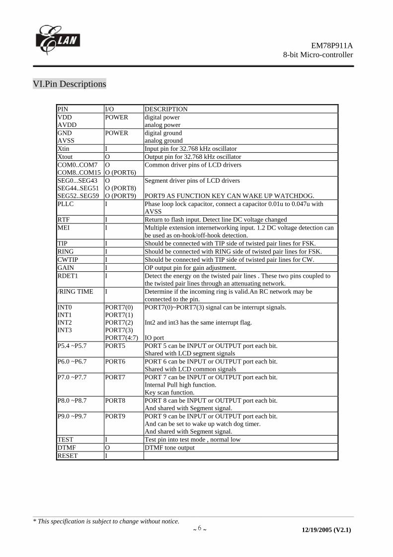
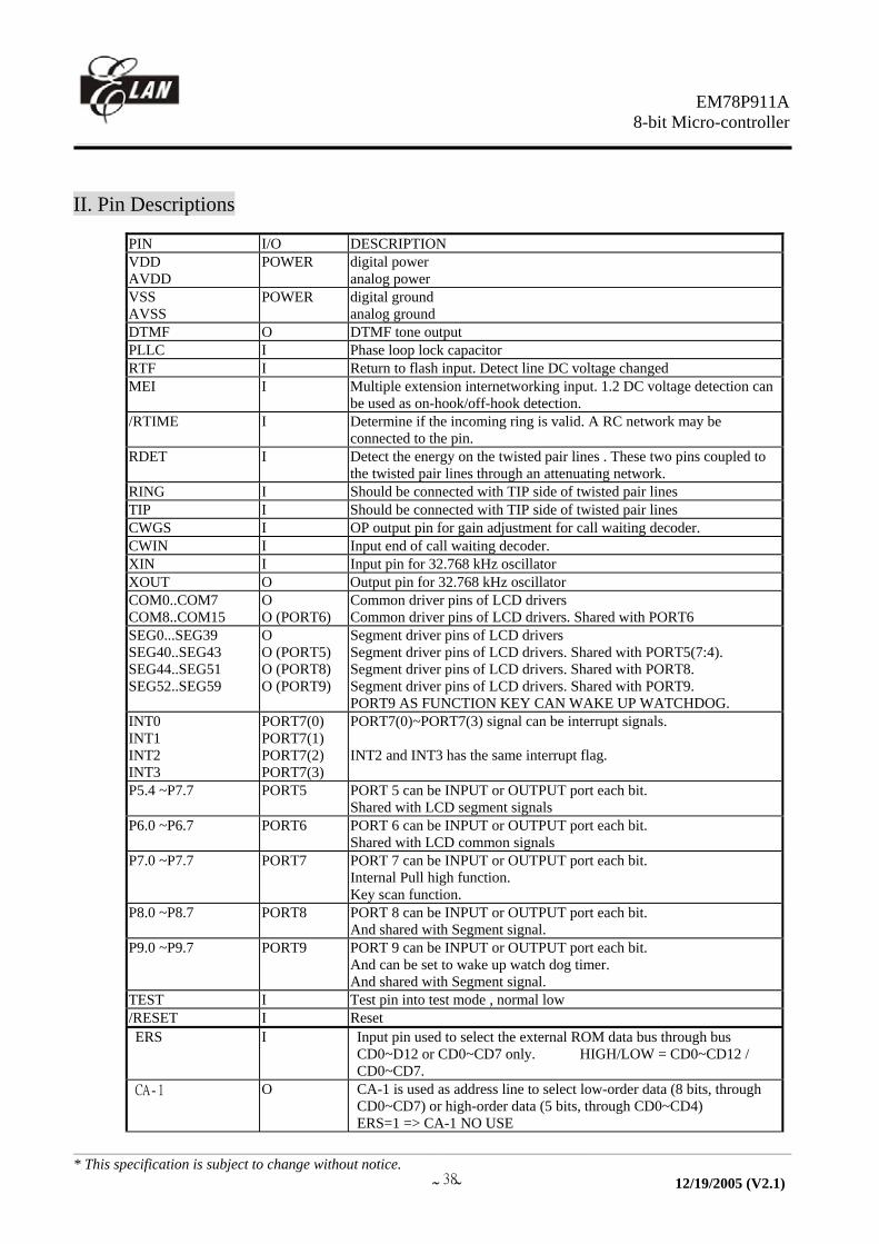
VI.Pin Descriptions
PIN I/O DESCRIPTION VDD AVDD
POWER digital power analog power
GND AVSS
POWER digital ground analog ground
Xtin I Input pin for 32.768 kHz oscillator Xtout O Output pin for 32.768 kHz oscillator COM0..COM7 COM8..COM15
O O (PORT6)
Common driver pins of LCD drivers
SEG0...SEG43 SEG44..SEG51 SEG52..SEG59
O O (PORT8) O (PORT9)
Segment driver pins of LCD drivers PORT9 AS FUNCTION KEY CAN WAKE UP WATCHDOG.
PLLC I Phase loop lock capacitor, connect a capacitor 0.01u to 0.047u with AVSS
RTF I Return to flash input. Detect line DC voltage changed MEI I Multiple extension internetworking input. 1.2 DC voltage detection can
be used as on-hook/off-hook detection. TIP I Should be connected with TIP side of twisted pair lines for FSK. RING I Should be connected with RING side of twisted pair lines for FSK. CWTIP I Should be connected with TIP side of twisted pair lines for CW. GAIN I OP output pin for gain adjustment. RDET1 I Detect the energy on the twisted pair lines . These two pins coupled to
the twisted pair lines through an attenuating network. /RING TIME I Determine if the incoming ring is valid.An RC network may be
connected to the pin. INT0 INT1 INT2 INT3
PORT7(0) PORT7(1) PORT7(2) PORT7(3) PORT7(4:7)
PORT7(0)~PORT7(3) signal can be interrupt signals. Int2 and int3 has the same interrupt flag. IO port
P5.4 ~P5.7 PORT5 PORT 5 can be INPUT or OUTPUT port each bit. Shared with LCD segment signals
P6.0 ~P6.7 PORT6 PORT 6 can be INPUT or OUTPUT port each bit. Shared with LCD common signals
P7.0 ~P7.7 PORT7 PORT 7 can be INPUT or OUTPUT port each bit. Internal Pull high function. Key scan function.
P8.0 ~P8.7 PORT8 PORT 8 can be INPUT or OUTPUT port each bit. And shared with Segment signal.
P9.0 ~P9.7 PORT9 PORT 9 can be INPUT or OUTPUT port each bit. And can be set to wake up watch dog timer. And shared with Segment signal.
TEST I Test pin into test mode , normal low DTMF O DTMF tone output RESET I
EM78P911A8-bit Micro-controller
__________________________________________________________________________________________________________________________________________________________________
* This specification is subject to change without notice. ~ ~ 7 12/19/2005 (V2.1)
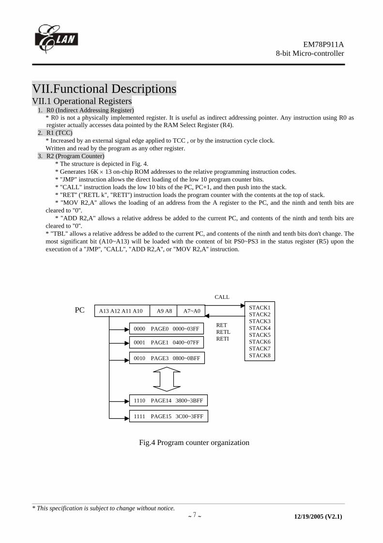
VII.Functional Descriptions VII.1 Operational Registers
1. R0 (Indirect Addressing Register) * R0 is not a physically implemented register. It is useful as indirect addressing pointer. Any instruction using R0 as register actually accesses data pointed by the RAM Select Register (R4).
2. R1 (TCC) * Increased by an external signal edge applied to TCC , or by the instruction cycle clock. Written and read by the program as any other register.
3. R2 (Program Counter) * The structure is depicted in Fig. 4. * Generates 16K × 13 on-chip ROM addresses to the relative programming instruction codes. * "JMP" instruction allows the direct loading of the low 10 program counter bits. * "CALL" instruction loads the low 10 bits of the PC, PC+1, and then push into the stack. * "RET'' ("RETL k", "RETI") instruction loads the program counter with the contents at the top of stack. * "MOV R2,A" allows the loading of an address from the A register to the PC, and the ninth and tenth bits are cleared to "0''. * "ADD R2,A" allows a relative address be added to the current PC, and contents of the ninth and tenth bits are cleared to "0''. * "TBL" allows a relative address be added to the current PC, and contents of the ninth and tenth bits don't change. The most significant bit (A10~A13) will be loaded with the content of bit PS0~PS3 in the status register (R5) upon the execution of a "JMP'', "CALL'', "ADD R2,A'', or "MOV R2,A'' instruction.
Fig.4 Program counter organization
PC A13 A12 A11 A10 A9 A8 A7~A0
0000 PAGE0 0000~03FF
0001 PAGE1 0400~07FF
1110 PAGE14 3800~3BFF
1111 PAGE15 3C00~3FFF
0010 PAGE3 0800~0BFF
STACK1STACK2STACK3STACK4STACK5STACK6STACK7STACK8
CALL
RETRETLRETI

EM78P911A8-bit Micro-controller
__________________________________________________________________________________________________________________________________________________________________
* This specification is subject to change without notice. ~ ~ 8 12/19/2005 (V2.1)
Fig.5 Data memory configuration
4. R3 (Status Register)
7 6 5 4 3 2 1 0 CAS PAGE /SDT T P Z DC C
* Bit 0 (C) Carry flag * Bit 1 (DC) Auxiliary carry flag * Bit 2 (Z) Zero flag * Bit 3 (P) Power down bit. Set to 1 during power on or by a "WDTC" command and reset to 0 by a "SLEP"
command. * Bit 4 (T) Time-out bit. Set to 1 by the "SLEP" and "WDTC" command, or during power up and reset to 0 by WDT
timeout.
EVENT T P REMARK
WDT wake up from sleep mode
0 0
WDT time out (not sleep mode) 0 1 /RESET wake up from sleep 1 0 power up 1 1 Low pulse on /RESET x x x .. don't care
* Bit 5 (/SDT) : (Read Only)(Stuttered dial tone signal detect output), 0/1 => SDT signal valid/SDT signal invalid * Bit 6 (PAGE) : change IOCB ~ IOCE to another page , 0/1 => page0 / page1
* Bit 7 (CAS) : CALL WAITING Output), 0/1= CW data valid/No data
5. R4 (RAM Select Register) * Bits 0 ~ 5 are used to select up to 64 registers in the indirect addressing mode. * Bits 6 ~ 7 determine which bank is activated among the 4 banks. * See the configuration of the data memory in Fig. 5.
000102030405060708090A0B0C0D0E0F
R0R1(TCC)R2(PC)R3(STATUS)R4(RSR)R5(ROM PAGE & R5)R6(PORT6)R7(PORT7)R8(PORT8)R9(PORT9)RA(CLK,FSK)RB(DTMF)RC(2.5K RAM ADDRESS)RD(2.5K RAM DATA)RE(WDT)RF(INT FLAG)
10:1F
16X8COMMONREGISTER
20:3F
BANK0 ~BANK332X8 ~32X8REGISTER
IOC6IOC7IOC8IOC9IOCAIOCB(LCD ADDRESS)IOCC(LCD DATA)IOCD(PULL HIGH)IOCE(IO, LCD)IOCF(INT CONTROL)
IOCB(COUNTER1)IOCC(COUNTER2)IOCD(R-OPTION)
page0
page1
BANK1 BANK2 …………..BANK10 256X8 256X8 …………….256X8
RC(ADDRESS) RD(DATA)
0:255
ADDRESS REGISTER CONTROL REGISTER(PAGE0)
CONTROL REGISTER(PAGE1)

EM78P911A8-bit Micro-controller
__________________________________________________________________________________________________________________________________________________________________
* This specification is subject to change without notice. ~ ~ 9 12/19/2005 (V2.1)
6. R5 (Program Page Select Register)
7 6 5 4 3 2 1 0 R57 R56 R55 R54 PS3 PS2 PS1 PS0
* Bit 0 (PS0) ~ 3 (PS3) Page select bits Page select bits
PS3 PS2 PS1 PS0 Program memory page (Address) 0 0 0 0 Page 0 0 0 0 1 Page 1 0 0 1 0 Page 2 0 0 1 1 Page 3 0 1 0 0 Page 4 0 1 0 1 Page 5 0 1 1 0 Page 6 0 1 1 1 Page 7 1 0 0 0 Page 8 1 0 0 1 Page 9 1 0 1 0 Page 10 1 0 1 1 Page 11 1 1 0 0 Page 12 1 1 0 1 Page 13 1 1 1 0 Page 14 1 1 1 1 Page 15
*User can use PAGE instruction to change page. To maintain program page by user. Otherwise, user can use far
jump (FJMP) or far call (FCALL) instructions to program user's code. And the program page is maintained by EMC's complier. It will change user's program by inserting instructions within program.
*Bit4~7 : PORT5 4-bit I/O register 6. R6 ~ R9 (Port 6 ~ Port 9)
* Four 8-bit I/O registers. 7. RA (FSK Status Register)(bit 0,1,2,4 read only)
7 6 5 4 3 2 1 0 IDLE /358E /LPD /LOW_BAT /FSKPWR DATA /CD /RD
* Bit0 (Read Only) (Ring detect signal) 0/1 : Ring Valid/Ring Invalid * Bit1(Read Only)(Carrier detect signal) 0/1 : Carrier Valid/Carrier Invalid * Bit2(Read Only)(FSK demodulator output signal) Fsk data transmitted in a baud rate 1200 Hz. * Bit3(read/write)(FSK block power up signal)
1/0 : FSK demodulator block power up/FSK demodulator power down When FSK is powered on, PLL is also enabled regardless of RA bit6(/358E). When FSK is powered off, PLL status is depended on RA bit6(/358E) setting.
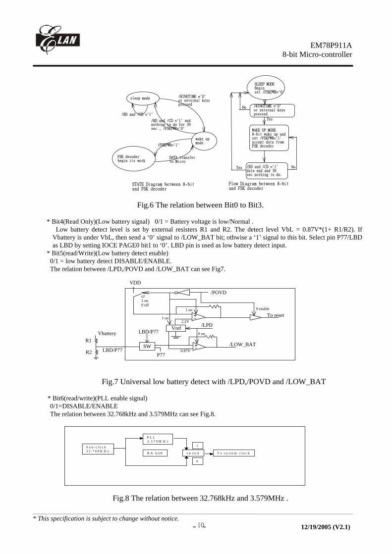
* The relation between Bit0 to Bit3 is shown in Fig.6.
EM78P911A8-bit Micro-controller
__________________________________________________________________________________________________________________________________________________________________
* This specification is subject to change without notice. ~ ~ 10 12/19/2005 (V2.1)
sleep mode
wake up mode
/RINGTIME ='0'
FSK decoderbegin its work
/FSKPWR='1'
DATA transfer to Micro
/RD and /CD ='1' andnothing to do for 30 sec , /FSKPWR='0'
or external keyspressed
/RD and /CD ='1'
SLEEP MODEBegin set /FSKPWR='0'
/RINGTIME ='0'or external keyspressed
WAKE UP MODE8-bit wake up and set /FSKPWR='1'accept data fromFSK decoder
/RD and /CD ='1'data end and 30sec nothing to do.
Yes No
No
Yes
STATE Diagram between 8-bit and FSK decoder
Flow Diagram between 8-bit and FSK decoder
Fig.6 The relation between Bit0 to Bit3.
* Bit4(Read Only)(Low battery signal) 0/1 = Battery voltage is low/Normal .
Low battery detect level is set by external resisters R1 and R2. The detect level VbL = 0.87V*(1+ R1/R2). If Vbattery is under VbL, then send a ‘0’ signal to /LOW_BAT bit; othwise a ‘1’ signal to this bit. Select pin P77/LBD as LBD by setting IOCE PAGE0 bit1 to ‘0’. LBD pin is used as low battery detect input.
* Bit5(read/Write)(Low battery detect enable) 0/1 = low battery detect DISABLE/ENABLE. The relation between /LPD,/POVD and /LOW_BAT can see Fig7.
Fig.7 Universal low battery detect with /LPD,/POVD and /LOW_BAT
* Bit6(read/write)(PLL enable signal) 0/1=DISABLE/ENABLE The relation between 32.768kHz and 3.579MHz can see Fig.8.
Fig.8 The relation between 32.768kHz and 3.579MHz .
S u b - c l o c k3 2 . 7 6 8 K H z
P L L3 . 5 7 9 M H z
R A b i t 6 s w i t c h T o s y s t e m c l o c k
1
0
VDD
Vref
s21 on0 off
1 onTo reset+-1 on
SWLBD/P77
P77
+-0.87V
/POVD
/LPDLBD/P77
/LOW_BAT
0 enable
0 onVbatteryR1
R2
2.2V
EM78P911A8-bit Micro-controller
__________________________________________________________________________________________________________________________________________________________________
* This specification is subject to change without notice. ~ ~ 11 12/19/2005 (V2.1)
* Bit7 IDLE: sleep mode selection bit 0/1=sleep mode/IDLE mode. This bit will decide SLEP instruction which mode to go. These two modes can be waken up by TCC clock or Watch Dog or PORT9 and run from “SLEP” next instruction.
Wakeup signal SLEEP mode IDLE mode GREEN mode NORMAL mode RA(7,6)=(0,0)
+ SLEP RA(7,6)=(1,0) + SLEP
RA(7,6)=(x,0) no SLEP
RA(7,6)=(x,1) no SLEP
TCC time out X Wake-up + Interrupt + Next instruction
Interrupt
Interrupt
WDT time out RESET Wake-up + Next instruction
RESET RESET
Port9 /RINGTIME pin
RESET Wake-up + Next instruction
X X
PORT70~73 X Wake-up + Interrupt + Next instruction
Interrupt
Interrupt
*P70 ~ P73 's wakeup function is controlled by IOCF(1,2,3) and ENI instruction. *P70 's wakeup signal is a rising or falling signal defined by CONT REGISTER bit7. */RINGTIME pin , Port9 ,Port71,Port72 and Port73 's wakeup signal is a falling edge signal.
8. RB(DTMF tone row and column register) (read/write)
7 6 5 4 3 2 1 0 c7 c6 c5 c4 r3 r2 r1 r0
* Bit 0 - Bit 3 are row-frequency tone. * Bit 4 - Bit 7 are column-frequency tone. * Initial RB is equal to high. Bit 7 ~ 0 are all "1" , turn off DTMF power .
bit 3~0 Row freq 1110 699.2Hz 1 2 3 A 1101 771.6Hz 4 5 6 B 1011 854Hz 7 8 9 C 0111 940.1Hz * 0 # D Column freq 1203Hz 1331.8Hz 1472Hz 1645.2Hz bit 7~4 1110 1101 1011 0111
9. RC(CALLER ID address)(read/write)
7 6 5 4 3 2 1 0 CIDA7 CIDA6 CIDA5 CIDA4 CIDA3 CIDA2 CIDA1 CIDA0
* Bit 0 ~ Bit 7 select CALLER ID RAM address up to 256. 10. RD(CALLER ID RAM data)(read/write) * Bit 0 ~ Bit 8 are CALLER ID RAM data transfer register. User can see IOCA register how to select CID RAM banks. 11. RE(LCD Driver,WDT Control)(read/write)
7 6 5 4 3 2 1 0 CWPWR /WDTE /WUP9H /WUP9L /WURING LCD_C2 LCD_C1 LCD_M
* Bit0 (LCD_M):LCD_M decides the methods, including duty, bias, and frame frequency. * Bit1~Bit2 (LCD_C#):LCD_C# decides the LCD display enable or blanking. change the display duty must set the "LCD_C2,LCD_C1" to "00".

EM78P911A8-bit Micro-controller
__________________________________________________________________________________________________________________________________________________________________
* This specification is subject to change without notice. ~ ~ 12 12/19/2005 (V2.1)
LCD_C2,LCD_C1 LCD Display Control LCD_M duty bias 0 0 change duty
Disable(turn off LCD) 0 1
1/16 1/4 1/8 1/4
0 1 Blanking : : 1 1 LCD display enable : :
* Bit3 (/WURING, RING Wake Up Enable): used to enable the wake-up function of /RINGTIME input pin. (1/0=enable/disable) * Bit4 (/WUP9L, PORT9 low nibble Wake Up Enable): used to enable the wake-up function of low nibble in PORT9.(1/0=enable/disable) * Bit5 (/WUP9H, PORT9 high nibble Wake Up Enable): used to enable the wake-up function of high nibble in PORT9.(1/0=enable/disable) * Bit6 (/WDTE,Watch Dog Timer Enable) Control bit used to enable Watchdog timer.(1/0=enable/disable) The relation between Bit3 to Bit6 can see the diagram 9. * Bit7(Power control of Call Waiting circuit)
(1/0=enable circuit /disable circuit) When Call waiting circuit is powered on, PLL is also enabled regardless of RA bit6(/358E). When Call waiting circuit is powered off, PLL status is depended on RA bit6(/358E) setting.
/WURING/RINGTIME
/WUP9LPORT9(3:0)
/WUP9HPORT9(7:4)
/WDTE
/WDTEN 0/1=enable/disable
Fig.9 Wake up function and control signal 12. RF (Interrupt Status Register)
7 6 5 4 3 2 1 0 INT3 FSK/CW C8_2 C8_1 INT2 INT1 INT0 TCIF
* "1" means interrupt request, "0" means non-interrupt * Bit 0 (TCIF) TCC timer overflow interrupt flag. Set when TCC timer overflows . * Bit 1 (INT0) external INT0 pin interrupt flag . * Bit 2 (INT1) external INT1 pin interrupt flag . * Bit 3 (INT2) external INT2pin interrupt flag . * Bit 4 (C8_1) internal 8 bit counter interrupt flag . * Bit 5 (C8_2) internal 8 bit counter interrupt flag . * Bit 6 ( FSK/CW ) FSK data or Call waiting data interrupt flag * Bit 7 (INT3) external INT3 pin interrupt flag. * High to low edge trigger , Refer to the Interrupt subsection. * IOCF is the interrupt mask register. User can read and clear.
13. R10~R3F (General Purpose Register)
* R10~R3F (Banks 0~3) all are general purpose registers.
VII.2 Special Purpose Registers 1. A (Accumulator)
* Internal data transfer, or instruction operand holding * It's not an addressable register.

EM78P911A8-bit Micro-controller
__________________________________________________________________________________________________________________________________________________________________
* This specification is subject to change without notice. ~ ~ 13 12/19/2005 (V2.1)
2. CONT (Control Register)
7 6 5 4 3 2 1 0 INT_EDGE INT TS TE PAB PSR2 PSR1 PSR0
* Bit 0 (PSR0) ~ Bit 2 (PSR2) TCC/WDT prescaler bits.
PSR2 PSR1 PSR0 TCC Rate WDT Rate 0 0 0 1:2 1:1 0 0 1 1:4 1:2 0 1 0 1:8 1:4 0 1 1 1:16 1:8 1 0 0 1:32 1:16 1 0 1 1:64 1:32 1 1 0 1:128 1:64 1 1 1 1:256 1:128
* Bit 3 (PAB) Prescaler assignment bit. 0/1 : TCC/WDT
* Bit 4 (TE) TCC signal edge 0: increment from low to high transition on TCC 1: increment from high to low transition on TCC
* Bit 5 (TS) TCC signal source 0: internal instruction cycle clock 1: 16.384KHz
* Bit 6 : (INT)INT enable flag 0: interrupt masked by DISI or hardware interrupt 1: interrupt enabled by ENI/RETI instructions
* Bit 7 : INT_EDGE 0:P70 's interruption source is a rising edge signal. 1:P70 's interruption source is a falling edge signal. * CONT register is readable and writable.
3. IOC5 (I/O Port Control Register) 7 6 5 4 3 2 1 0
IOC57 IOC56 IOC55 IOC54 MEIO RTFO RTFPWR P5S * Bit0: P5S is switch register for I/O port or LCD signal switching. 0/1= normal I/O port/SEGMENT output . * Bit1(RTFPWR) : power control of RTF circuit, 1/0 => power on/power off * Bit2(RTFO) : (Read Only) RTF line DC voltage change detect output.
When line DC voltage is not changed, RTFO is low. * Bit3(MEIO) : MEI line high or line in-use detect output
When input voltage of MEI pin is below 1.2V, MEIO is low; when input voltage of MEI pin is over 1.3V, MEIO is high.
* Bit 4 to Bit7 are PORT5 I/O direction control registers. * "1" put the relative I/O pin into high impedance, while "0" put the relative I/O pin as output.
4. IOC6 ~ IOC9 (I/O Port Control Register)
* four I/O direction control registers. * "1" put the relative I/O pin into high impedance, while "0" put the relative I/O pin as output. * User can see IOCB register how to switch to normal I/O port.

EM78P911A8-bit Micro-controller
__________________________________________________________________________________________________________________________________________________________________
* This specification is subject to change without notice. ~ ~ 14 12/19/2005 (V2.1)
5. IOCA (CALLER ID RAM,IO ,PAGE Control Register)(read/write,initial "00000000")
7 6 5 4 3 2 1 0 P8SH P8SL SDTPW/0 CALL_4 CALL_3 CALL_2 CALL_1 MEIPWR
* Bit 0(MEIPWR) : power control of MEI circuit, 1/0 => power on/power off * Bit4~Bit1:"000" to "1001" are ten blocks of CALLER ID RAM area. User can use 2.5K RAM with RD ram
address. * Bit 5 (SDTPW/0) : (Power control of Stuttered dial tone circuit/disable SDT)
ps. When code option bit2(/SDTEN) is “1”, SDT is disabled and IOCA bit5 is always “0”. User cannot use SDT function. When code option bit2(/SDTEN) is “0”, SDT is enabled and IOCA bit5 is SDTPW. At this time, setting SDTPW 1/0 = power on circuit /power down circuit.
* Bit6: port8 low nibble switch, 0/1= normal I/O port/SEGMENT output . * Bit7: port8 high nibble switch , 0/1= normal I/O port/SEGMENT output
6. IOCB (LCD ADDRESS) PAGE0 : Bit6 ~ Bit0 = LCDA6 ~ LCDA0
The LCD display data is stored in the data RAM . The relation of data area and COM/SEG pin is as below:
COM15 ~ COM8 COM7 ~ COM0 40H (Bit15 ~ Bit8) 00H (Bit7 ~ Bit0) SEG0 41H 01H SEG1 : : : : : : : : : : : : 7AH 4AH SEG58 7BH 3BH SEG59 7CH 3CH Empty : : : 7FH 3FH Empty
PAGE1 : 8 bit up-counter (COUNTER1) preset and read out register . ( write = preset ) . After a interruption , it will count from “00”. 7. IOCC (LCD DATA) PAGE0 : Bit7 ~ Bit0 = LCD RAM data register PAGE1 : 8 bit up-counter (COUNTER2) preset and read out register . ( write = preset) After a interruption , it will count from “00”. 8. IOCD (Pull-high Control Register) PAGE0:
7 6 5 4 3 2 1 0 PH7 PH6 PH5 PH4 PH3 PH2 PH1 PH0
* Bit 0 ~ 7 (/PH#) Control bit used to enable the pull-high of PORT7(#) pin. 1: Enable internal pull-high 0: Disable internal pull-high
PAGE1: 7 6 5 4 3 2 1 0
RO7 RO6 RO5 RO4 RO3 RO2 RO1 RO0
EM78P911A8-bit Micro-controller
__________________________________________________________________________________________________________________________________________________________________
* This specification is subject to change without notice. ~ ~ 15 12/19/2005 (V2.1)
* Bit 7 ~ 0 (RO7~0) Control bit used to enable the R-OPTION of PORT97~PORT90 pin. 1: Enable 0: Disable RO is used for R-OPTION . Setting RO to ‘1’ will enable the status of R-option pin (P90 ~ P97) to read by controller. Clearing RO will disable R-option function. If the R-option function is used, user must connect PORT9 pins to GND by 560K external register . If the register is connected/disconnected , the R9 will read as “ 0/1” when RO is set to ‘1’.
9. IOCE (Bias,PLL Control Register) PAGE0 :
7 6 5 4 3 2 1 0 P9SH P9SL P6S Bias3 Bias2 Bias1 LBD/P77 SC
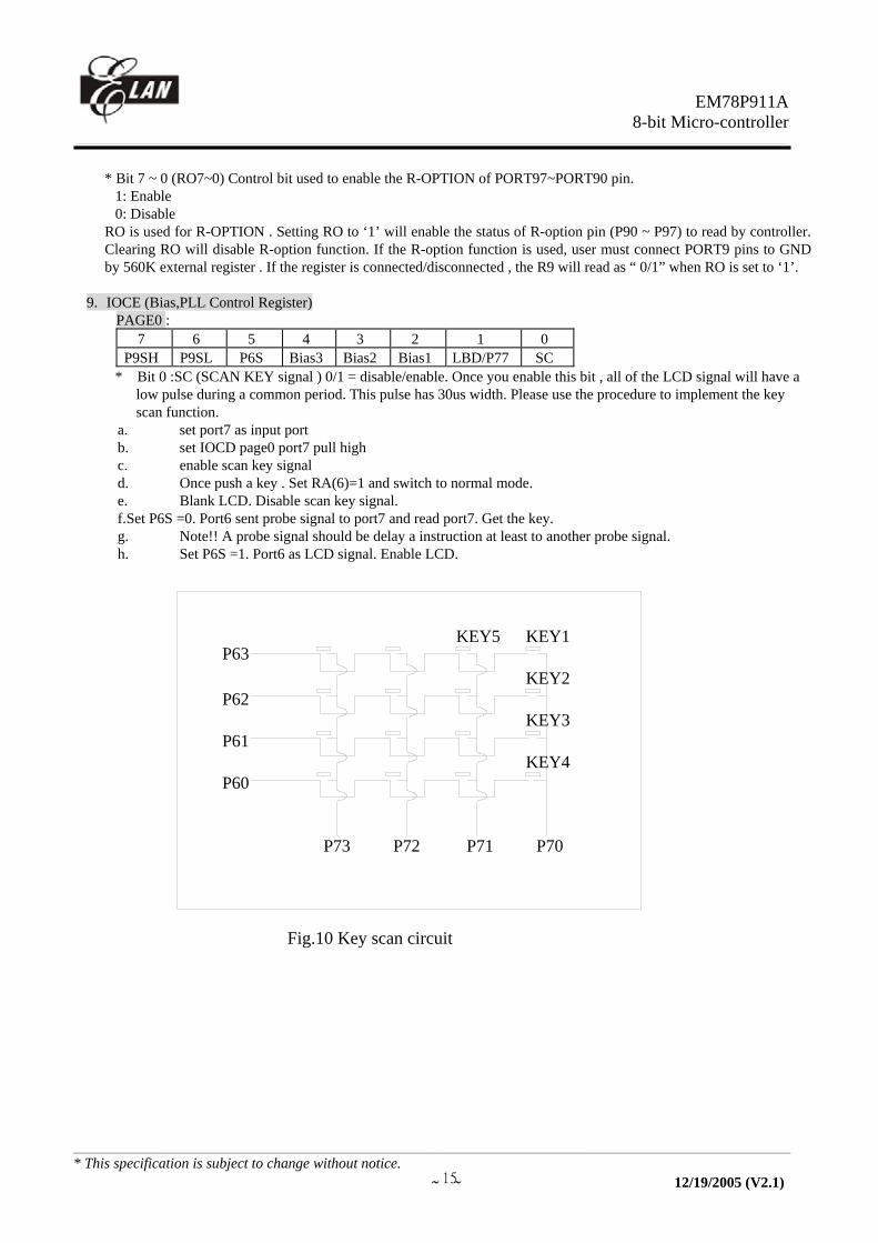
* Bit 0 :SC (SCAN KEY signal ) 0/1 = disable/enable. Once you enable this bit , all of the LCD signal will have a low pulse during a common period. This pulse has 30us width. Please use the procedure to implement the key scan function.
a. set port7 as input port b. set IOCD page0 port7 pull high c. enable scan key signal d. Once push a key . Set RA(6)=1 and switch to normal mode. e. Blank LCD. Disable scan key signal. f. Set P6S =0. Port6 sent probe signal to port7 and read port7. Get the key. g. Note!! A probe signal should be delay a instruction at least to another probe signal. h. Set P6S =1. Port6 as LCD signal. Enable LCD.
Fig.10 Key scan circuit
P70P71P72P73
P60
P61
P62
P63KEY1
KEY2
KEY5
KEY3
KEY4

EM78P911A8-bit Micro-controller
__________________________________________________________________________________________________________________________________________________________________
* This specification is subject to change without notice. ~ ~ 16 12/19/2005 (V2.1)
Fig.11 key scan signal * Bit 1 (LBD/P77) : (Port7’s P77 switch), 0/1 => low battery detect input/ normal IO port P77
ps. Default value is ‘1’. * Bit 2~4 (Bias1~Bias3) Control bits used to choose LCD operation voltage .
LCD operate voltage Vop (VDD 5V) VDD=5V 000 001 010 011 100 101 110 111
0.60VDD 0.66VDD 0.74VDD 0.82VDD 0.87VDD 0.93VDD 0.96VDD 1.00VDD
3.0V 3.3V 3.7V 4.0V 4.4V 4.7V 4.8V 5.0V
* Bit5:port6 switch , 0/1= normal I/O port/COMMON output * Bit6:port9 low nibble switch , 0/1= normal I/O port/SEGMENT output . Bit7:port9 high nibble switch
PAGE1 :
7 6 5 4 3 2 1 0 OP77 OP76 C2S C1S PSC1 PSC0 CDRD 0
* Bit0: unused * Bit1: cooked data or raw data select bit , 0/1 ==> cooked data/raw data * Bit3~Bit2: counter1 prescaler , reset=(0,0) (PSC1,PSC0) = (0,0)=>1:1 , (0,1)=>1:4 , (1,0)=>1:8 , (1,1)=>reserved * Bit4:counter1 source , (0/1)=(32768Hz/3.579MHz if enable) scale=1:1 * Bit5:counter2 source , (0/1)=(32768Hz/3.579MHz if enable) scale=1:1 * Bit6:P76 opendrain control (0/1)=(disable/enable) * Bit7:P77 opendrain control (0/1)=(disable/enable)
com2
seg
vddv1v2v3vlcdGnd
vddv1v2v3vlcdGnd
30us

EM78P911A8-bit Micro-controller
__________________________________________________________________________________________________________________________________________________________________
* This specification is subject to change without notice. ~ ~ 17 12/19/2005 (V2.1)
10. IOCF (Interrupt Mask Register)
7 6 5 4 3 2 1 0 INT3 FSK/CW C8_2 C8_1 INT2 INT1 INT0 TCIF
* Bit 0 ~ 7 interrupt enable bit.
0: disable interrupt 1: enable interrupt
* IOCF Register is readable and writable.
VII.3 TCC/WDT Prescaler There is an 8-bit counter available as prescaler for the TCC or WDT. The prescaler is available for the TCC only or WDT only at the same time.
• An 8 bit counter is available for TCC or WDT determined by the status of the bit 3 (PAB) of the CONT register. • See the prescaler ratio in CONT register. • Fig. 10 depicts the circuit diagram of TCC/WDT. • Both TCC and prescaler will be cleared by instructions which write to TCC each time. • The prescaler will be cleared by the WDTC and SLEP instructions, when assigned to WDT mode. • The prescaler will not be cleared by SLEP instructions, when assigned to TCC mode.
Fig.10 Block diagram of TCC WDT
VII.4 I/O Ports The I/O registers, Port 6 ~ Port 9, are bi-directional tri-state I/O ports. Port 7 can be pulled-high internally by software control. The I/O ports can be defined as "input" or "output" pins by the I/O control registers (IOC6 ~ IOC9 ) under program control. The I/O registers and I/O control registers are both readable and writable. The I/O interface circuit is shown in Fig.11.
16.38KHz

EM78P911A8-bit Micro-controller
__________________________________________________________________________________________________________________________________________________________________
* This specification is subject to change without notice. ~ ~ 18 12/19/2005 (V2.1)
Fig.11 The circuit of I/O port and I/O control register
VII.5 RESET and Wake-up The RESET can be caused by
(1) Power on reset, or Voltage detector (2) WDT timeout. (if enabled and in GREEN or NORMAL mode) Note that only Power on reset, or only Voltage detector in Case(1) is enabled in the system by CODE Option bit. If Voltage detector is disabled, Power on reset is selected in Case (1). Refer to Fig. 12.
Fig.12 Block diagram of Reset of controller
Once the RESET occurs, the following functions are performed. • The oscillator is running, or will be started. • The Program Counter (R2) is set to all "0". • When power on, the upper 3 bits of R3 and the upper 2 bits of R4 are cleared. • The Watchdog timer and prescaler are cleared. • The Watchdog timer is disabled. • The CONT register is set to all "1" • The other register (bit7..bit0)

EM78P911A8-bit Micro-controller
__________________________________________________________________________________________________________________________________________________________________
* This specification is subject to change without notice. ~ ~ 19 12/19/2005 (V2.1)
R5 = “xxxx0000” IOC5 = "1111xx00" R6 = PORT IOC6 = "11111111" R7 = PORT IOC7 = "11111111" R8 = PORT IOC8 = "11111111" R9 = PORT IOC9 = "11111111" RA = "000x0xxx IOCA = "00000000" RB = "11111111" Page0 IOCB = "00000000" Page1 IOCB = "00000000"RC = "00000000" Page0 IOCC = "0xxxxxxx" Page1 IOCC = "00000000"RD = "xxxxxxxx" Page0 IOCD = "00000000" Page1 IOCD = “00000000”RE = "00000000" Page0 IOCE = "00000010" Page1 IOCE = "00000000"RF = "00000000" IOCF = "00000000"
The controller can be awakened from SLEEP mode or IDLE mode (execution of "SLEP" instruction, named as
SLEEP MODE or IDLE mode) by (1)TCC time out (2) WDT time-out (if enabled) or, (3) external input at PORT9. The three cases will cause the controller wake up and run from next instruction. After wake-up , user should control WATCH DOG in case of reset in GREEN mode or NORMAL mode. The last two should be open RE register before into sleep mode or IDLE mode . The first one case will set a flag in RF bit0 .But it will not go to address 0x08.
VII.6 Interrupt
The CALLER ID IC has internal interrupts which are falling edge triggered, as followed : TCC timer overflow interrupt (internal) , two 8-bit counters overflow interrupt . If these interrupt sources change signal from high to low , then RF register will generate '1' flag to corresponding register if you enable IOCF register. RF is the interrupt status register which records the interrupt request in flag bit. IOCF is the interrupt mask register. Global interrupt is enabled by ENI instruction and is disabled by DISI instruction. When one of the interrupts (when enabled) generated, will cause the next instruction to be fetched from address 008H. Once in the interrupt service routine the source of the interrupt can be determined by polling the flag bits in the RF register. The interrupt flag bit must be cleared in software before leaving the interrupt service routine and enabling interrupts to avoid recursive interrupts. There are four external interrupt pins including INT0 , INT1 , INT2 , INT3 . And four internal interrupt available. Internal signals include TCC,CNT1,CNT2,FSK and CALL WAITING data. The last two will generate a interrupt when the data trasient from high to low. External interrupt INT0 , INT1 , INT2 , INT3 signals are from PORT7 bit0 to bit3 . If IOCF is enable then these signal will cause interrupt , or these signals will be treated as general input data . After reset, the next instruction will be fetched from address 000H and the instruction inturrept is 001H and the hardware inturrept is 008H.
TCC will go to address 0x08 in GREEN mode or NORMAL mode after time out. And it will run next instruction from “SLEP” instruction. These two cases will set a RF flag.
It is very important to save ACC,R3 and R5 when processing a interruption.
Address Instruction Note 0x08 DISI ;Disable interrupt 0x09 MOV A_BUFFER,A ;Save ACC 0x0A SWAP A_BUFFER 0x0B SWAPA 0x03 ;Save R3 status 0x0C MOV R3_BUFFER,A 0x0D MOV A,0x05 ;Save ROM page register 0x0E MOV R5_BUFFER,A : : : : : MOV A,R5_BUFFER ;Return R5 : MOV 0X05,A : SWAPA R3_BUFFER ;Return R3

EM78P911A8-bit Micro-controller
__________________________________________________________________________________________________________________________________________________________________
* This specification is subject to change without notice. ~ ~ 20 12/19/2005 (V2.1)
: MOV 0X03,A : SWAPA A_BUFFER ;Return ACC : RETI
VII.7 Instruction Set Instruction set has the following features: (1). Every bit of any register can be set, cleared, or tested directly. (2). The I/O register can be regarded as general register. That is, the same instruction can operates on I/O register. The symbol "R" represents a register designator which specifies which one of the 64 registers (including operational registers and general purpose registers) is to be utilized by the instruction. Bits 6 and 7 in R4 determine the selected register bank. "b'' represents a bit field designator which selects the number of the bit, located in the register "R'', affected by the operation. "k'' represents an 8 or 10-bit constant or literal value.
INSTRUCTION BINARY HEX
MNEMONIC
OPERATION
STATUS AFFECTED
0 0000 0000 0000 0000 NOP No Operation None 0 0000 0000 0001 0001 DAA Decimal Adjust A C 0 0000 0000 0010 0002 CONTW A → CONT None 0 0000 0000 0011 0003 SLEP 0 → WDT, Stop oscillator T,P 0 0000 0000 0100 0004 WDTC 0 → WDT T,P 0 0000 0000 rrrr 000r IOW R A → IOCR None 0 0000 0001 0000 0010 ENI Enable Interrupt None 0 0000 0001 0001 0011 DISI Disable Interrupt None 0 0000 0001 0010 0012 RET [Top of Stack] → PC None 0 0000 0001 0011 0013 RETI [Top of Stack] → PC
Enable Interrupt None
0 0000 0001 0100 0014 CONTR CONT → A None 0 0000 0001 rrrr 001r IOR R IOCR → A None 0 0000 0010 0000 0020 TBL R2+A → R2 bits 9,10 do not
clear Z,C,DC
0 0000 01rr rrrr 00rr MOV R,A A → R None 0 0000 1000 0000 0080 CLRA 0 → A Z 0 0000 11rr rrrr 00rr CLR R 0 → R Z 0 0001 00rr rrrr 01rr SUB A,R R-A → A Z,C,DC 0 0001 01rr rrrr 01rr SUB R,A R-A → R Z,C,DC 0 0001 10rr rrrr 01rr DECA R R-1 → A Z 0 0001 11rr rrrr 01rr DEC R R-1 → R Z 0 0010 00rr rrrr 02rr OR A,R A ∨ VR → A Z 0 0010 01rr rrrr 02rr OR R,A A ∨ VR → R Z 0 0010 10rr rrrr 02rr AND A,R A & R → A Z 0 0010 11rr rrrr 02rr AND R,A A & R → R Z 0 0011 00rr rrrr 03rr XOR A,R A ⊕ R → A Z 0 0011 01rr rrrr 03rr XOR R,A A ⊕ R → R Z 0 0011 10rr rrrr 03rr ADD A,R A + R → A Z,C,DC 0 0011 11rr rrrr 03rr ADD R,A A + R → R Z,C,DC 0 0100 00rr rrrr 04rr MOV A,R R → A Z 0 0100 01rr rrrr 04rr MOV R,R R → R Z 0 0100 10rr rrrr 04rr COMA R /R → A Z 0 0100 11rr rrrr 04rr COM R /R → R Z 0 0101 00rr rrrr 05rr INCA R R+1 → A Z

EM78P911A8-bit Micro-controller
__________________________________________________________________________________________________________________________________________________________________
* This specification is subject to change without notice. ~ ~ 21 12/19/2005 (V2.1)
0 0101 01rr rrrr 05rr INC R R+1 → R Z 0 0101 10rr rrrr 05rr DJZA R R-1 → A, skip if zero None 0 0101 11rr rrrr 05rr DJZ R R-1 → R, skip if zero None 0 0110 00rr rrrr 06rr RRCA R R(n) → A(n-1)
R(0) → C, C → A(7) C
0 0110 01rr rrrr 06rr RRC R R(n) → R(n-1) R(0) → C, C → R(7)
C
0 0110 10rr rrrr 06rr RLCA R R(n) → A(n+1) R(7) → C, C → A(0)
C
0 0110 11rr rrrr 06rr RLC R R(n) → R(n+1) R(7) → C, C → R(0)
C
0 0111 00rr rrrr 07rr SWAPA R R(0-3) → A(4-7) R(4-7) → A(0-3)
None
0 0111 01rr rrrr 07rr SWAP R R(0-3) ↔ R(4-7) None 0 0111 10rr rrrr 07rr JZA R R+1 → A, skip if zero None 0 0111 11rr rrrr 07rr JZ R R+1 → R, skip if zero None 0 100b bbrr rrrr 0xxx BC R,b 0 → R(b) None 0 101b bbrr rrrr 0xxx BS R,b 1 → R(b) None 0 110b bbrr rrrr 0xxx JBC R,b if R(b)=0, skip None 0 111b bbrr rrrr 0xxx JBS R,b if R(b)=1, skip None 1 00kk kkkk kkkk 1kkk CALL k PC+1 → [SP]
(Page, k) → PC None
1 01kk kkkk kkkk 1kkk JMP k (Page, k) → PC None 1 1000 kkkk kkkk 18kk MOV A,k k → A None 1 1001 kkkk kkkk 19kk OR A,k A ∨ k → A Z 1 1010 kkkk kkkk 1Akk AND A,k A & k → A Z 1 1011 kkkk kkkk 1Bkk XOR A,k A ⊕ k → A Z 1 1100 kkkk kkkk 1Ckk RETL k k → A, [Top of Stack] → PC None 1 1101 kkkk kkkk 1Dkk SUB A,k k-A → A Z,C,DC 1 1110 0000 0001 1E01 INT PC+1 → [SP]
001H → PC None
1 1110 1000 kkkk 1E8k PAGE k K->R5(3:0) None 1 1111 kkkk kkkk 1Fkk ADD A,k k+A → A Z,C,DC
VII.8 Option VII.8.1 CODE Option Register
The CALLER ID IC has one CODE option register which is not part of the normal program memory. The option bits cannot be accessed during normal program execution.
7 6 5 4 3 2 1 0 - - - /RTFEN /MEIEN /SDTEN /PROT MCLK
* Bit 0 (MCLK) : main clock selection. 0/1 = 1.79MHZ / 3.58MHZ * Bit 1 (/PROT) : Code protection bit
0 : protection enable 1 : protection disable
* Bit 2 (/SDTEN) : Stuttered dial tone disabled/enable 0: enable 1: disable
* Bit 3 (/MEIEN) : MEI function, 0/1 => enable/disable MEI function When MEI function is disabled, MEI is always powered down and user cannot use this function.
* Bit 4 (/RTFEN) : RTF function, 0/1 => enable/disable RTF function When RTF function is disabled, RTF is always powered down and user cannot use this function.

EM78P911A8-bit Micro-controller
__________________________________________________________________________________________________________________________________________________________________
* This specification is subject to change without notice. ~ ~ 22 12/19/2005 (V2.1)
* Bits 5~7 : unused
VII.8.2 PAD Option /POVD(power on voltage detect) reset can be enabled/disabled by PAD Option. This POVD pad is not shown on
the pin assignment. Internally or externally connecting this pad to GND/VDD to enable/disable /POVD reset. /POVD 2.2V reset power on reset Low power
detect without reset
Low power detect controlled by RA(5)
sleep mode current
1 No yes Yes Yes 1uA 0 yes yes Yes yes 15uA

EM78P911A8-bit Micro-controller
__________________________________________________________________________________________________________________________________________________________________
* This specification is subject to change without notice. ~ ~ 23 12/19/2005 (V2.1)
VII.9 FSK FUNCTION VII.9.1 Functional Block Diagram
Fig.13 FSK Block Diagram
VII.9.2 Function Descriptions The CALLER ID IC is a CMOS device designed to support the Caller Number Deliver feature which is offered by the Regional Bell Operating Companies.The FSK block comprises two paths: the signal path and the ring indicator path. The signal path consist of an input differential buffer,a band pass filter, an FSK demodulator and a data valid with carrier detect circuit. The ring detector path includes a clock generator, a ring detect circuit . In a typical application, the ring detector maintains the line continuously while all other functions of the chip are inhibited. If a ring signal is sent, the /RINGTIME pin will has a low signal. User can use this signal to wake up whole chip or read /RD signal from RA register. A /FSKPWR input is provided to activate the block regardless of the presence of a power ring signal. If /FSKPWR is sent low, the FSK block will power down whenever it detects a valid ring signal, it will power on when /FSKPWR is high. The input buffer accepts a differential AC coupled input signal through the TIP and RING input and feeds this signal to a band pass filter. Once the signal is filtered, the FSK demodulator decodes the information and sends it to a post filter. The output data is then made available at DATA OUT pin. This data, as sent by the central office, includes the header information (alternate "1" and "0") and 150 ms of marking which precedes the date , time and calling number. If no data is present, the DATA OUT pin is held in a high state. This is accomplished by an carrier detect circuit which determines if the in-band energy is high enough. If the incoming signal is valid and thus the demodulated data is transferred to DATA OUT pin . If it is not, then the FSK demodulator is blocked.
RingDetCircuit
Ring det1
Tip
Ring
PowerUp
FSKdemodul
Data ValidEnergy DetCircuit
DATA OUT
/CD
CLOCKOSC inOSC out
/RD
/Ring Time
Band PassFilter
/FSKPWR

EM78P911A8-bit Micro-controller
__________________________________________________________________________________________________________________________________________________________________
* This specification is subject to change without notice. ~ ~ 24 12/19/2005 (V2.1)
VII.9.3 Ring detect circuit
When Vdd is applied to the circuit, the RC network will charge cap C1 to Vdd holding /RING TIME off . The resistor network R2 to R3 attenuates the incoming power ring applied to the top of R2. The values given have been chosen to provide a sufficient voltage at DET1 pin, to turn on the Schmitt trigger input. When Vt+ of the Schmitt is exceeded, cap C1 will discharge. The value of R1 and C1 must be chosen to hold the /RING TIME pin voltage below the Vt+ of the Schmitt between the individual cycle of the power ring. With /RINGTIME enabled, this signal will be a /RD signal in RA throught a buffer.
Fig.14 ring detect circuit
VII.10 DTMF ( Dual Tone Multi Frequency ) Tone Generator Built-in DTMF generator can generate dialing tone signals for telephone of dialing tone type. There are two kinds of DTMF tone . One is the group of row frequency, the other is the group of column frequency, each group has 4 kinds of frequency , user can get 16 kinds of DTMF frequency totally. DTMF generator contains a row frequency sine wave generator for generating the DTMF signal which selected by low order 4 bits of RB and a column frequency sine wave generator for generating the DTMF signal which selected by high order 4 bits of RB. This block can generate single tone by filling one bit zero to this register. If all the values are high , the power of DTMF will turn off until one or two low values. Either high or low 4 bits must be set by an effective value, otherwise, if any ineffective value or both 4 bits are load effective value, tone output will be disable. Recommend value refer to table as follow please :
Vdd/Ring Time
Det1
/RDC1
R3
R1
R2
/Ring Time

EM78P911A8-bit Micro-controller
__________________________________________________________________________________________________________________________________________________________________
* This specification is subject to change without notice. ~ ~ 25 12/19/2005 (V2.1)
SYSTEM CLOCK
DTMF low-freqselection
DTMF high-freqselection
Sine wave generator
Sine wave generator
Adder
ROWRegister
COLUMNRegister
Low frequency generator
High frequency generator
DTMF toneoutput
Fig.15 DTMF Block Diagram * RB ( DTMF Register ) . Bit 0 - Bit 3 are row-frequency tone. . Bit 4 - Bit 7 are column-frequency tone. . Initial RB is equal to HIGH. . Except below values of RB ,the other values of RB are not effect. If RB is set by ineffective value, the DTMF output will be disable and there is no tone output. . Bit 7 ~ 0 are all "1" , turn off DTMF power .
bit 3~0 Row freq 1110 699.2Hz 1 2 3 A 1101 771.6Hz 4 5 6 B 1011 854Hz 7 8 9 C 0111 940.1Hz * 0 # D Column freq 1203Hz 1331.8Hz 1472Hz 1645.2Hz bit 7~4 1110 1101 1011 0111
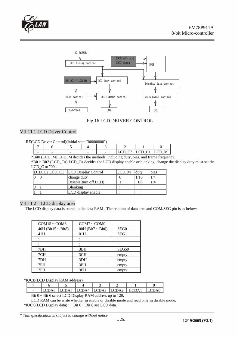
VII.11 LCD Driver The CALLER ID IC can drive LCD directly and has 60 segments and 16 commons that can drive 60*16 dots totally. LCD block is made up of LCD driver , display RAM, segment output pins , common output pins and LCD operating power supply pins. Duty , bias , the number of segment , the number of common and frame frequency are determined by LCD mode register . LCD control register. The basic structure contains a timing control which uses the basic frequency 32.768KHz to generate the proper timing for different duty and display access. RE register is a command register for LCD driver, the LCD display( disable, enable, blanking) is controlled by LCD_C and the driving duty and bias is decided by LCD_M and the display data is stored in data RAM which address and data access controlled by registers IOCB and IOCC.
EM78P911A8-bit Micro-controller
__________________________________________________________________________________________________________________________________________________________________
* This specification is subject to change without notice. ~ ~ 26 12/19/2005 (V2.1)
Fig.16 LCD DRIVER CONTROL
VII.11.1 LCD Driver Control
RE(LCD Driver Control)(initial state "00000000")
7 6 5 4 3 2 1 0 - - - - - LCD_C2 LCD_C1 LCD_M
*Bit0 (LCD_M):LCD_M decides the methods, including duty, bias, and frame frequency. *Bit1~Bit2 (LCD_C#):LCD_C# decides the LCD display enable or blanking. change the display duty must set the LCD_C to "00".
LCD_C2,LCD_C1 LCD Display Control LCD_M duty bias 0 0 change duty
Disable(turn off LCD) 0 1
1/16 1/4 1/8 1/4
0 1 Blanking : : 1 1 LCD display enable : :
VII.11.2 LCD display area
The LCD display data is stored in the data RAM . The relation of data area and COM/SEG pin is as below:
COM15 ~ COM8 COM7 ~ COM0 40H (Bit15 ~ Bit8) 00H (Bit7 ~ Bit0) SEG0 41H 01H SEG1 : : : : : : 7BH 3BH SEG59 7CH 3CH empty 7DH 3DH empty 7EH 3EH empty 7FH 3FH empty
*IOCB(LCD Display RAM address)
7 6 5 4 3 2 1 0 - LCDA6 LCDA5 LCDA4 LCDA3 LCDA2 LCDA1 LCDA0
Bit 0 ~ Bit 6 select LCD Display RAM address up to 120. LCD RAM can be write whether in enable or disable mode and read only in disable mode.
*IOCC(LCD Display data) : Bit 0 ~ Bit 8 are LCD data.
LCD timing control
RE(LCD_C,LCD_M)
Bias control
Vdd-Vlcd
LCD duty control
LCD COMMON control
COM
RAM
IOCB(address)
IOCC(data)
Display data control
LCD SEGMENT control
SEG
32.768KHz
EM78P911A8-bit Micro-controller
__________________________________________________________________________________________________________________________________________________________________
* This specification is subject to change without notice. ~ ~ 27 12/19/2005 (V2.1)
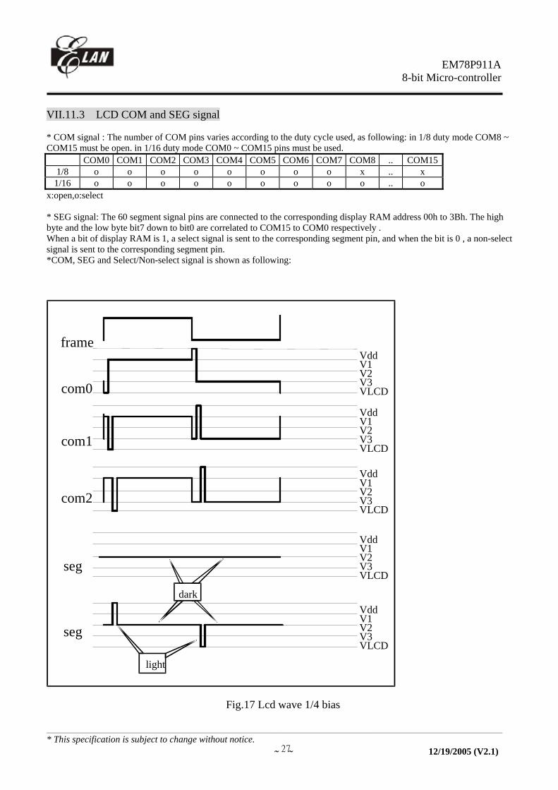
VII.11.3 LCD COM and SEG signal * COM signal : The number of COM pins varies according to the duty cycle used, as following: in 1/8 duty mode COM8 ~ COM15 must be open. in 1/16 duty mode COM0 ~ COM15 pins must be used.
COM0 COM1 COM2 COM3 COM4 COM5 COM6 COM7 COM8 .. COM15 1/8 o o o o o o o o x .. x
1/16 o o o o o o o o o .. o x:open,o:select * SEG signal: The 60 segment signal pins are connected to the corresponding display RAM address 00h to 3Bh. The high byte and the low byte bit7 down to bit0 are correlated to COM15 to COM0 respectively . When a bit of display RAM is 1, a select signal is sent to the corresponding segment pin, and when the bit is 0 , a non-select signal is sent to the corresponding segment pin. *COM, SEG and Select/Non-select signal is shown as following:
Fig.17 Lcd wave 1/4 bias
VddV1V2V3VLCD
frame
com0
com1
com2
seg
seg
light
dark
VddV1V2V3VLCD
VddV1V2V3VLCD
VddV1V2V3VLCD
VddV1V2V3VLCD

EM78P911A8-bit Micro-controller
__________________________________________________________________________________________________________________________________________________________________
* This specification is subject to change without notice. ~ ~ 28 12/19/2005 (V2.1)
VII.11.4 LCD Bias control
IOCE (Bias Control Register) 7 6 5 4 3 2 1 0 Bias3 Bias2 Bias1
* Bit 2~4 (Bias1~Bias3) Control bits used to choose LCD operation voltage . The circuit can refer ti figure15. LCD operate voltage Vop (VDD 5V) VDD=5V
000 001 010 011 100 101 110 111
0.60VDD 0.66VDD 0.74VDD 0.82VDD 0.87VDD 0.93VDD 0.96VDD 1.00VDD
3.0V 3.3V 3.7V 4.0V 4.4V 4.7V 4.8V 5.0V
* Bit 5~7 unused
78810/78910
Vdd
Vlcd
Vop
Vss
Vop=Vdd-VlcdR=1K
R
R
R
R
V1
V2
V3
MUXBias3~1
000
001
010
011
100
101
110
111
::
8.2R
0.4R
0.4R
0.3R
0.3R
0.2R
0.1R
0.1R
Fig.18 LCD bias circuit
EM78P911A8-bit Micro-controller
__________________________________________________________________________________________________________________________________________________________________
* This specification is subject to change without notice. ~ ~ 29 12/19/2005 (V2.1)
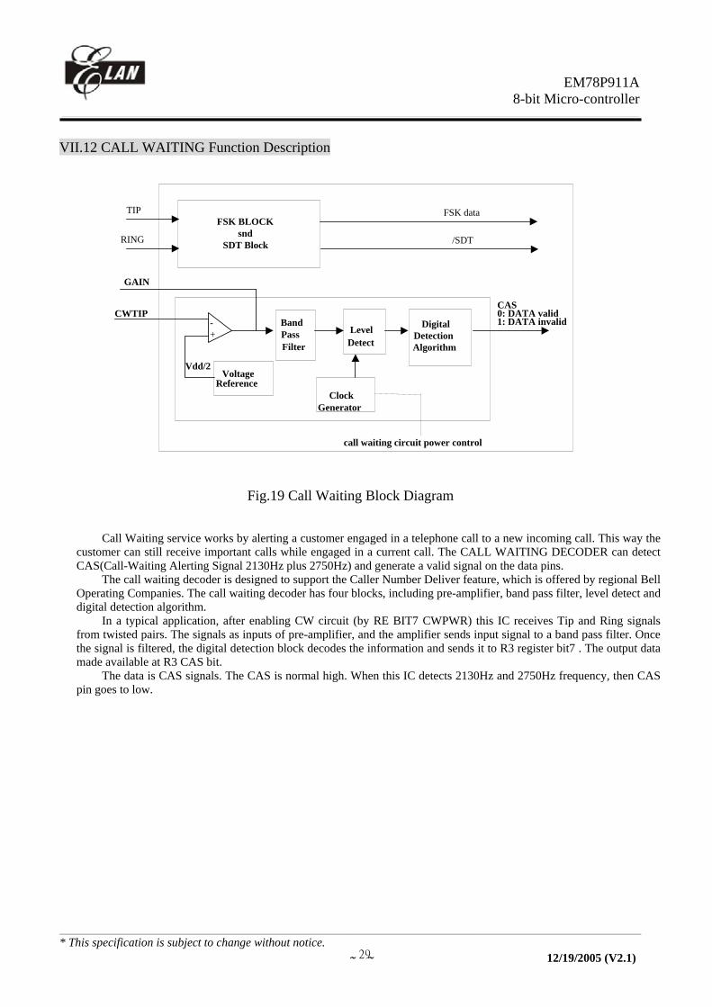
VII.12 CALL WAITING Function Description
Fig.19 Call Waiting Block Diagram
Call Waiting service works by alerting a customer engaged in a telephone call to a new incoming call. This way the
customer can still receive important calls while engaged in a current call. The CALL WAITING DECODER can detect CAS(Call-Waiting Alerting Signal 2130Hz plus 2750Hz) and generate a valid signal on the data pins.
The call waiting decoder is designed to support the Caller Number Deliver feature, which is offered by regional Bell Operating Companies. The call waiting decoder has four blocks, including pre-amplifier, band pass filter, level detect and digital detection algorithm.
In a typical application, after enabling CW circuit (by RE BIT7 CWPWR) this IC receives Tip and Ring signals from twisted pairs. The signals as inputs of pre-amplifier, and the amplifier sends input signal to a band pass filter. Once the signal is filtered, the digital detection block decodes the information and sends it to R3 register bit7 . The output data made available at R3 CAS bit.
The data is CAS signals. The CAS is normal high. When this IC detects 2130Hz and 2750Hz frequency, then CAS pin goes to low.
CWTIP
Filter
DigitalDetectionAlgorithm
Vdd/2
BandPass
DetectLevel
VoltageReference
ClockGenerator
GAIN
CAS0: DATA valid1: DATA invalid
call waiting circuit power control
FSK BLOCKsnd
SDT Block
TIP
RING
-+
FSK data
/SDT

EM78P911A8-bit Micro-controller
__________________________________________________________________________________________________________________________________________________________________
* This specification is subject to change without notice. ~ ~ 30 12/19/2005 (V2.1)
VII.13 Stuttered dial tone (SDT) Function Description
Fig.17 Stuttered dial tone block diagram
SDT(Stuttered dial tone) circuit and FSK circuit use the same input OP Amp. When SDTPW bit (bit5 of register
IOCA) is set, SDT circuit is powered on and SDT detection is enabled. SDT detection enabled means it is powered on and detect 350Hz plus 440Hz dual tone frequency. And SDT signal detection output is sent to /SDT bit (bit5 of register R3) with low enable.
If SDT circuit works, it consists of high-band and low-band band pass tone filters, level detect, frequency counting and digital algorithm to qualify correct timing.
VII.14 MEI and RTF Function Description
Based on TIA/EIA-777(or TIA SP-4078) protocol, MEI(Multiple Extension Internetworking) allows Type 2 (and 3)
CPE to dynamically arbitrate responsibility for completing the CAS-ACK handshake. Also, RTF(Request to Flash) allows Type 2 (and 3) CPE to synchronize line flash signal after CAS-ACK handshaking.
For MEI part, protocol shows line voltage below 19V as line-in use(phone off-hook status) and voltage above 21V as line high(phone on-hook status). MEI circuit works as on-hook/off-hook detection and internal transition voltage is 1.2V. Use two external resistors to reduce line DC voltage into MEI input pin. These has a little voltage transition hysteresis to complete the rule.
For RTF part, protocol shows 0.5V line DC voltage change detection and timing to be followed(see the protocol for details). RTF circuit can detect this little DC voltage change and complete the same timing as protocol shown.
TIPRING FSK Block
Stuttered dailtone
Detection Block
/SDT
FSK data
/CD
1.2V
1.2M
20M
RTF
MEIO
RTFO
MEI
VDD
330k
RTF220k105
3.3M 333
VDD

EM78P911A8-bit Micro-controller
__________________________________________________________________________________________________________________________________________________________________
* This specification is subject to change without notice. ~ ~ 31 12/19/2005 (V2.1)
VIII.Absolute Operation Maximum Ratings
RATING SYMBOL VALUE UNIT DC SUPPLY VOLTAGE Vdd -0.3 To 6 V INPUT VOLTAGE Vin -0.5 TO Vdd +0.5 V OPERATING TEMPERATURE RANGE Ta 0 TO 70
IX DC Electrical Characteristic (Ta=0°C ~ 70°C, VDD=5V±5%, VSS=0V) (VDD=2.5V to 6V for CPU ; VDD=3.5V to 6V for FSK ; VDD=2.5V to 6V for DTMF )
Symbol Parameter Condition Min Typ Max Unit IIL1 Input Leakage Current for
input pins VIN = VDD, VSS ±1 µA
IIL2 Input Leakage Current for bi-directional pins
VIN = VDD, VSS ±1 µA
VIH Input High Voltage 2.5 V VIL Input Low Voltage 0.8 V VIHT Input High Threshold
Voltage /RESET, TCC, RDET1 2.0 V
VILT Input Low Threshold Voltage
/RESET, TCC,RDET1 0.8 V
VIHX Clock Input High Voltage OSCI 3.5 V VILX Clock Input Low Voltage OSCI 1.5 V VHscan Key scan Input High Voltage Port6 for key scan 3.5 V VLscan Key scan Input Low Voltage Port6 for key scan 1.5 V VOH1 Output High Voltage
(port6,7,8) IOH = -1.6mA 2.4 V
(port9) IOH = -6.0mA 2.4 V VOL1 Output Low Voltage
(port6,7,8) IOL = 1.6mA 0.4 V
(port9) IOL = 5.0mA 0.4 V Vcom Com voltage drop Io=+/- 50 uA - - 2.9 V Vseg Segment voltage drop Io=+/- 50 uA - - 3.8 V Vlcd LCD drive reference voltage Contrast adjustment IPH Pull-high current Pull-high active input pin at
VSS -10 -15 µA
ISB1 Power down current (SLEEP mode)
All input and I/O pin at VDD, output pin floating, WDT disabled
1 4 µA
ISB2 Low clock current (FREEN mode)
CLK=32.768KHz, FSK, DTMF, CW block disable , All input and I/O pin at VDD, output pin floating, WDT disabled, LCD enable
80 100 µA
ICC Operating supply current (NORMAL mode)
/RESET=High, CLK=3.579MHz, output pin floating,LCD enable, FSK, DTMF, CW Fblock disable
1.5 1.8 mA
EM78P911A8-bit Micro-controller
__________________________________________________________________________________________________________________________________________________________________
* This specification is subject to change without notice. ~ ~ 32 12/19/2005 (V2.1)
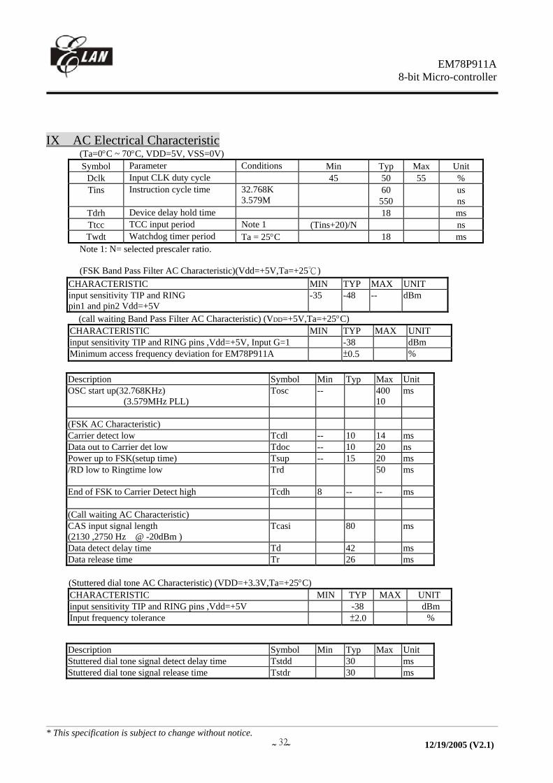
IX AC Electrical Characteristic (Ta=0°C ~ 70°C, VDD=5V, VSS=0V)
Symbol Parameter Conditions Min Typ Max Unit Dclk Input CLK duty cycle 45 50 55 % Tins Instruction cycle time 32.768K
3.579M
60 550
us ns
Tdrh Device delay hold time 18 ms Ttcc TCC input period Note 1 (Tins+20)/N ns Twdt Watchdog timer period Ta = 25°C 18 ms
Note 1: N= selected prescaler ratio. (FSK Band Pass Filter AC Characteristic)(Vdd=+5V,Ta=+25)
CHARACTERISTIC MIN TYP MAX UNIT input sensitivity TIP and RING pin1 and pin2 Vdd=+5V
-35 -48 -- dBm
(call waiting Band Pass Filter AC Characteristic) (VDD=+5V,Ta=+25°C) CHARACTERISTIC MIN TYP MAX UNIT input sensitivity TIP and RING pins ,Vdd=+5V, Input G=1 -38 dBm Minimum access frequency deviation for EM78P911A ±0.5 %
Description Symbol Min Typ Max Unit OSC start up(32.768KHz) (3.579MHz PLL)
Tosc -- 400 10
ms
(FSK AC Characteristic) Carrier detect low Tcdl -- 10 14 ms Data out to Carrier det low Tdoc -- 10 20 ns Power up to FSK(setup time) Tsup -- 15 20 ms /RD low to Ringtime low Trd 50 ms
End of FSK to Carrier Detect high Tcdh 8 -- -- ms (Call waiting AC Characteristic) CAS input signal length (2130 ,2750 Hz @ -20dBm )
Tcasi 80 ms
Data detect delay time Td 42 ms Data release time Tr 26 ms
(Stuttered dial tone AC Characteristic) (VDD=+3.3V,Ta=+25°C) CHARACTERISTIC MIN TYP MAX UNIT input sensitivity TIP and RING pins ,Vdd=+5V -38 dBm Input frequency tolerance ±2.0 %
Description Symbol Min Typ Max Unit Stuttered dial tone signal detect delay time Tstdd 30 ms Stuttered dial tone signal release time Tstdr 30 ms
EM78P911A8-bit Micro-controller
__________________________________________________________________________________________________________________________________________________________________
* This specification is subject to change without notice. ~ ~ 33 12/19/2005 (V2.1)
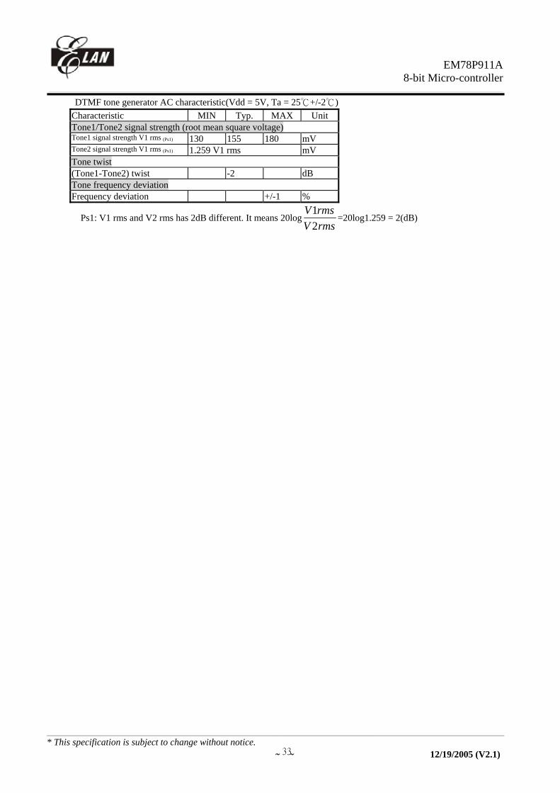
DTMF tone generator AC characteristic(Vdd = 5V, Ta = 25+/-2) Characteristic MIN Typ. MAX Unit Tone1/Tone2 signal strength (root mean square voltage) Tone1 signal strength V1 rms (Ps1) 130 155 180 mV Tone2 signal strength V1 rms (Ps1) 1.259 V1 rms mV Tone twist (Tone1-Tone2) twist -2 dB Tone frequency deviation Frequency deviation +/-1 %
Ps1: V1 rms and V2 rms has 2dB different. It means 20logrmsVrmsV
21
=20log1.259 = 2(dB)
EM78P911A8-bit Micro-controller
__________________________________________________________________________________________________________________________________________________________________
* This specification is subject to change without notice. ~ ~ 34 12/19/2005 (V2.1)
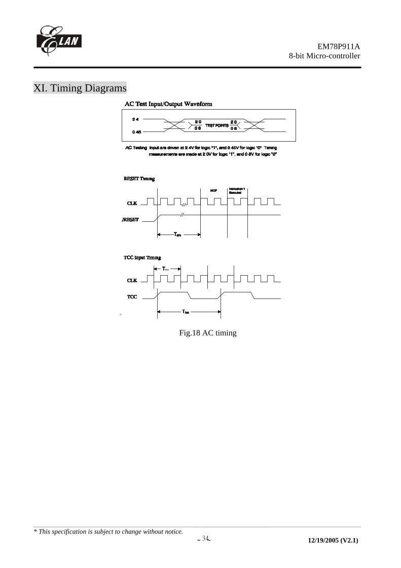
XI. Timing Diagrams
`
ins
Fig.18 AC timing

EM78P911A8-bit Micro-controller
__________________________________________________________________________________________________________________________________________________________________
* This specification is subject to change without notice. ~ ~ 35 12/19/2005 (V2.1)
Fig.19 FSK Timing Diagram
Fig.20 Call Waiting Timing Diagram
Fig.21 Stuttered dial tone detect. timing diagram
PCWPower power off power onon/off
events
Td
plug inon hook
in use
CASTcasi
CAS Tr
normal
TIP/RING
/RING TIME
/RD
/CD
DATA
OSC
FIRST RING2 SECONDS 0.5 SEC 0.5 SEC
SECOND RING2 SECONDS
DATA
3.579 MHz
Tcdl
/358E
Tosc
Tdoc
Tpd
Tsup
TcdhTrd
TIP/RING
/SDT
SDTsignal
tsdtd tsdtr
SDTsignal
SDTsignal
SDTsignal

EM78P911A8-bit Micro-controller
__________________________________________________________________________________________________________________________________________________________________
* This specification is subject to change without notice. ~ ~ 36 12/19/2005 (V2.1)
XII. Application Circuit
Note: If FSK sensitivity is poor, user can connect 1M ohms resistor between TIP
pin and RING pin.
Fig.21 APPLICATION CIRCUIT
1 2 3 4
A
B
C
D
4321
D
C
B
ATitle
Number RevisionSize
A
Date: 18-May-1999 Sheet of File: C:\ADVSCH\78911_1.SCH Drawn By:
TIP
RING
DET1
RINGTIME
AVSS
VSS
TEST
CWTIP
GAIN
COMMONSEGMENT
AVDDVDD
ESTST/GT
PLLC
XIN
XOUT
RESET
LCD DISPLAY
0.22u270K
VDD
470K
33K
10K
10K
300K
100
32768
0.01u
27
0.1u
0.1u
0.1u 250V
0.1u 250V
FUSE
1000P
1000PTIP
RING
TO PHONE
VSS
DET1
VDD
VSS
AVSS
VSS
27
100K
100K
470K
NPN
0.1u
VDD
MATCHING NETWORK10K
10K
103

EM78P911A8-bit Micro-controller
__________________________________________________________________________________________________________________________________________________________________
* This specification is subject to change without notice. ~ ~ 37 12/19/2005 (V2.1)
Appendex : EM78R911A SPEC. I. Pin Configuration
Fig1. Pin Assignment
12345678910111213141516171819202122232425262728293031323334353637383940
80797877767574737271706968676665646362616059585756555453525150494847464544434241
12011911811711611511411311211111010910810710610510410310210110099989796959493929190898887868584838281
121122123124125126127128129130131132133134135136137138139140141142143144145146147148149150151152153154155156157158159160
TEST
SEG44/P80
SEG45/P81
SEG46/P82
SEG47/P83
SEG48/P84
SEG49/P85
SEG50/P86
SEG51/P87
SEG52/P90
SEG53/P91
SEG54/P92
SEG55/P93
SEG56/P94
SEG57/P95
SEG58/P96
SEG59/P97
VD
D
R32K
VSS
IOD
0IO
D1
IOD
2IO
D3
IOD
4IO
D5
IOD
6IO
D7
INSEN
DIR
SELPH
1OU
TX
2OU
T/H
OLD
/POV
DEN
TCC
MC
LK
SEG39SEG38SEG37SEG36LBD/P77P76P75P74P73/INT3P72/INT2P71/INT1P70/INT0
COM15/P67COM14/P66COM13/P65COM12/P64COM11/P63COM10/P62COM9/P61COM8/P60NCNCCOM7COM6COM5COM4COM3COM2COM1COM0SEG35SEG34SEG33SEG32SEG31
SEG29
SEG28
SEG27
SEG26
SEG25
SEG24
SEG23
SEG22
SEG21
SEG20
NC
VSS
CD
12C
D11
CD
10C
D9
CD
8C
D7
CD
6C
D5
CD
4C
D3
CD
2C
D1
CD
0
CA
13C
A12
CA
11C
A10
CA
9C
A8
CA
7C
A6
CA
5C
A4
CA
3C
A2
CA
1
AVSSDTMFPLLC
/RTIMERDETRING
TIPCWGSCWIN
XINXOUT
AVDD
SEG0SEG1SEG2SEG3SEG4SEG5SEG6SEG7SEG8SEG9
NCNC
SEG10
VDD
ERSCA-1CA0
RTFMEI
CW
FS
SEG40/P54
CA
14
SEG41/P55SEG42/P56
/RESET
NC
SEG11SEG12
SEG13SEG14SEG15SEG16SEG17SEG18SEG19
VD
D
SEG30
VSS
SEG43/P57
EM78P911A8-bit Micro-controller
__________________________________________________________________________________________________________________________________________________________________
* This specification is subject to change without notice. ~ ~ 38 12/19/2005 (V2.1)
II. Pin Descriptions
PIN I/O DESCRIPTION VDD AVDD
POWER digital power analog power
VSS AVSS
POWER digital ground analog ground
DTMF O DTMF tone output PLLC I Phase loop lock capacitor RTF I Return to flash input. Detect line DC voltage changed MEI I Multiple extension internetworking input. 1.2 DC voltage detection can
be used as on-hook/off-hook detection. /RTIME I Determine if the incoming ring is valid. A RC network may be
connected to the pin. RDET I Detect the energy on the twisted pair lines . These two pins coupled to
the twisted pair lines through an attenuating network. RING I Should be connected with TIP side of twisted pair lines TIP I Should be connected with TIP side of twisted pair lines CWGS I OP output pin for gain adjustment for call waiting decoder. CWIN I Input end of call waiting decoder. XIN I Input pin for 32.768 kHz oscillator XOUT O Output pin for 32.768 kHz oscillator COM0..COM7 COM8..COM15
O O (PORT6)
Common driver pins of LCD drivers Common driver pins of LCD drivers. Shared with PORT6
SEG0...SEG39 SEG40..SEG43 SEG44..SEG51 SEG52..SEG59
O O (PORT5) O (PORT8) O (PORT9)
Segment driver pins of LCD drivers Segment driver pins of LCD drivers. Shared with PORT5(7:4). Segment driver pins of LCD drivers. Shared with PORT8. Segment driver pins of LCD drivers. Shared with PORT9. PORT9 AS FUNCTION KEY CAN WAKE UP WATCHDOG.
INT0 INT1 INT2 INT3
PORT7(0) PORT7(1) PORT7(2) PORT7(3)
PORT7(0)~PORT7(3) signal can be interrupt signals. INT2 and INT3 has the same interrupt flag.
P5.4 ~P7.7 PORT5 PORT 5 can be INPUT or OUTPUT port each bit. Shared with LCD segment signals
P6.0 ~P6.7 PORT6 PORT 6 can be INPUT or OUTPUT port each bit. Shared with LCD common signals
P7.0 ~P7.7 PORT7 PORT 7 can be INPUT or OUTPUT port each bit. Internal Pull high function. Key scan function.
P8.0 ~P8.7 PORT8 PORT 8 can be INPUT or OUTPUT port each bit. And shared with Segment signal.
P9.0 ~P9.7 PORT9 PORT 9 can be INPUT or OUTPUT port each bit. And can be set to wake up watch dog timer. And shared with Segment signal.
TEST I Test pin into test mode , normal low /RESET I Reset ERS I Input pin used to select the external ROM data bus through bus
CD0~D12 or CD0~CD7 only. HIGH/LOW = CD0~CD12 / CD0~CD7.
CA-1 O CA-1 is used as address line to select low-order data (8 bits, through CD0~CD7) or high-order data (5 bits, through CD0~CD4) ERS=1 => CA-1 NO USE

EM78P911A8-bit Micro-controller
__________________________________________________________________________________________________________________________________________________________________
* This specification is subject to change without notice. ~ ~ 39 12/19/2005 (V2.1)
ERS=0 => CA-1=0 HIGH ORDER DATA CA-1=1 LOW ORDER DATA
CA0~CA14 O Program code address bus. CA0~CA14 are address output pins for external programming ROM access.
CD0~CD12 I Data access in terms of CA0 ~ CA12 addressing. IOD0~IOD7 O I/O data bus. INSEND O Used to indicate the instruction completion and ready for next
instruction. IRSEL O IRSEL is an output pin used to select an external EVEN/ODD ROM. PH1OUT O Phase 1 output X2OUT O System clock output. /HOLD I Microcontroller hold request. /POVD I Input pin used to enable Power on voltage detector.
Power on voltage detector is enabled if /POVD is low. Power on voltage detector is disabled if /POVD is high. Also see the following table.
ENTCC I TCC control pin with internal pull-high (560KΩ). TCC works normally when ENTCC is high, and TCC counting is stopped when ENTCC is low.
MCLK I Input pin for main clock selection. Internal pull low through a register.
CWFS I Minimum access frequency range for call waiting CAS tone. Frequency range is +/-0.5% if CWFS is low. Frequency range is +/- 1.5% if CWFS is high.
R32k I R5 register setting option 4-bit page selection and 4-bit PORT5 I/O can be access if R32k is low. 5-bit page selection and 5-bit PORT5 I/O can be access if R32k is high Also see section III for operational register R5 in the following.
POVD status table /POVD 2.2V reset power on reset Low power
detect without reset
Low power detect controlled by RA(5)
sleep mode current
1 No yes Yes Yes 1uA 0 Yes yes Yes yes 15uA
III. Operational registers R5 (Program Page Select Register)
(1) If R32k pin is low level, the R5 register is as follows. 7 6 5 4 3 2 1 0
R57 R56 R55 R54 PS3 PS2 PS1 PS0 * Bit 0 (PS0) ~ 3 (PS3) Page select bits
Page select bits PS3 PS2 PS1 PS0 Program memory page (Address)
0 0 0 0 Page 0 0 0 0 1 Page 1 0 0 1 0 Page 2

EM78P911A8-bit Micro-controller
__________________________________________________________________________________________________________________________________________________________________
* This specification is subject to change without notice. ~ ~ 40 12/19/2005 (V2.1)
0 0 1 1 Page 3 : : : : : : : : : : 1 1 0 1 Page 13 1 1 1 0 Page 14 1 1 1 1 Page 15
*User can use PAGE instruction to change page. To maintain program page by user. Otherwise, user can use far jump (FJMP) or far call (FCALL) instructions to program user's code. And the program page is maintained by EMC's complier. It will change user's program by inserting instructions within program.
* Bit 7 (R57) ~ Bit 4 (R54) : 4-bit I/O register for PORT5(7:4). (2) If R32k pin is high level, the R5 register is as follows.
7 6 5 4 3 2 1 0 R57 R56 R55 PS4 PS3 PS2 PS1 PS0
* Bit 0 (PS0) ~ 4 (PS4) Page select bits Page select bits PS4 PS3 PS2 PS1 PS0 Program memory page (Address)
0 0 0 0 0 Page 0 0 0 0 0 1 Page 1 0 0 0 1 0 Page 2 0 0 0 1 1 Page 3 : : : : : : : : : : : : 1 1 1 0 1 Page 29 1 1 1 1 0 Page 30 1 1 1 1 1 Page 31
*User can use PAGE instruction to change page. To maintain program page by user. Otherwise, user can use far jump (FJMP) or far call (FCALL) instructions to program user's code. And the program page is maintained by EMC's complier. It will change user's program by inserting instructions within program.
* Bit 7 (R57) ~ Bit 5 (R55) : 3-bit I/O register for PORT5(7:5).
IOCA * Bit 5 (SDTPW) : (Power control of Stuttered dial tone circuit/disable SDT)
1/0 power on circuit /power down circuit.
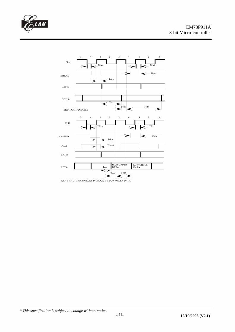
IV. AC Electrical Characteristic
Tdiea Delay from Phase 3 end to INSEND active
Cl=100pF 30 ns
Tdiei Delay from Phase 4 end to INSEND inactive
Cl=100pF 30 ns
Tiew INSEND pulse width 30 ns Tdca Delay from Phase 4 end to
CA Bus valid C1=100pF 30 ns
Tacc ROM data access time 100 ns Tcds ROM data setup time 20 ns Tcdh ROM data hold time 20 ns Tdca-1 Delay time of CA-1 C1=100pF 30 ns
Note 1: N= selected prescaler ratio.
EM78P911A8-bit Micro-controller
__________________________________________________________________________________________________________________________________________________________________
* This specification is subject to change without notice. ~ ~ 41 12/19/2005 (V2.1)
CLK
3 4 1 2 3 4 1 2 3
/INSEND
Tdiea Tdiei
Tiew
Tdca
CA14:0
Tacc
Tcds
CD12:0
Tcdh
CLK
3 4 1 2 3 4 1 2 3
/INSEND
Tdiea Tdiei
TiewTdca
CA14:0
Tacc
Tcds
CD7:0
Tcdh
CA-1
HIGH ORDERDATA
LOW ORDERDATA
ERS=0 CA-1=0 HIGH ORDER DATA CA-1=1 LOW ORDER DATA
ERS=1 CA-1=DISABLE
Tdca-1