product / process change notice...the above information is the exclusive intellectual property of...
TRANSCRIPT

The above information is the exclusive intellectual property of Winbond Electronics and shall not be disclosed, distributed or reproduced without permission from Winbond.
Table No.: 1110-0001-08-A
Product / Process Change Notice
No.: Z200-PCN-DM201912-05-A Date: December 20, 2019
Change Title : W25Q128JW “J-Series” (F58) to replace W25Q128FW “F-Series” (F58) 128Mb 1.8V SpiFlash® Memories
Change Classification: Major Minor with customer notification Minor without customer notification Change item : Design Raw Material Wafer FAB Assembly Testing Packing Others
Affected Product(s) :
Please refer to Table 1 in details.
Description of Change(s)
The W25Q128JW 128Mb SpiFlash® Memories use Winbond’s F58 Flash technology. It is function-compatible with W25Q128FW F58 devices offering improved performance, features and availability.
a) Command backward compatible with W25Q128FW (same Superset Instruction Set)
b) Clock operation up to 133MHz
c) Support DTR with Max. frequency up to 66MHz
d) SPI with Single / Dual / Quad / QPI
e) Flexible architecture with 4KB sectors
f) Support low power consumption compared to W25Q128FW
g) Support fast programing compared to W25Q128FW
Reason for Change(s) :
Improve features, cost, and keep command backward compatible with W25Q128FW (same Superset Instruction Set).
Impact of Change(s) : ( positive & negative )
Form : Change No change except WLCSP package form. (Please refer to attachment I)
Fit : Change No change except WLCSP package form. (Please refer to attachment I)
Function : No Concern (Please refer to attachment II)
Reliability : No Concern (Please refer to attachment III)
Hazardous Substances: No Concern (Please refer to attachment IV)
Qualification Plan/ Results :
Based on Winbond W25Q128JW Serial Flash Reliability report, the new product meets our criteria and no quality concern(refer to Attachment III in details)
The above information is the exclusive intellectual property of Winbond Electronics and shall not be disclosed, distributed or reproduced without permission from Winbond.
Table No.: 1110-0001-08-A
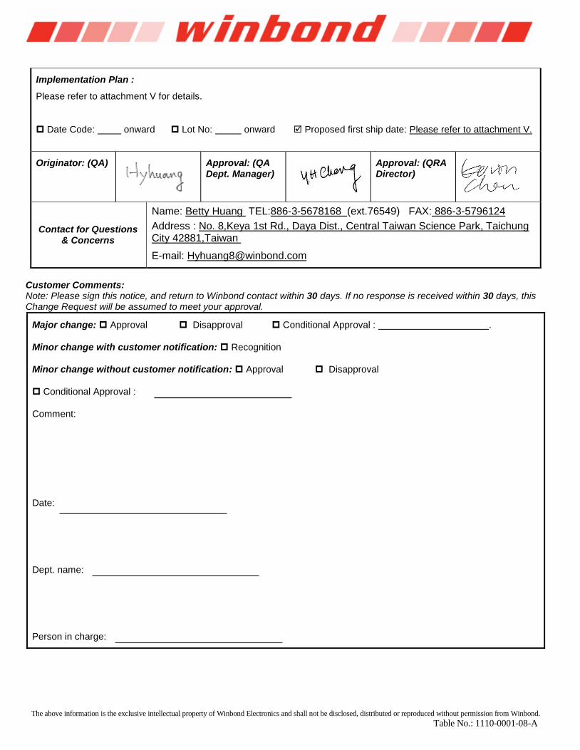
Implementation Plan :
Please refer to attachment V for details.
Date Code: onward Lot No: onward Proposed first ship date: Please refer to attachment V.
Originator: (QA)
Approval: (QA Dept. Manager)
Approval: (QRA Director)
Contact for Questions & Concerns
Name: Betty Huang TEL:886-3-5678168 (ext.76549) FAX: 886-3-5796124
Address : No. 8,Keya 1st Rd., Daya Dist., Central Taiwan Science Park, Taichung City 42881,Taiwan
E-mail: [email protected]
Customer Comments: Note: Please sign this notice, and return to Winbond contact within 30 days. If no response is received within 30 days, this Change Request will be assumed to meet your approval.
Major change: Approval Disapproval Conditional Approval : .
Minor change with customer notification: Recognition
Minor change without customer notification: Approval Disapproval
Conditional Approval :
Comment:
Date:
Dept. name:
Person in charge:
The above information is the exclusive intellectual property of Winbond Electronics and shall not be disclosed, distributed or reproduced without permission from Winbond.
Table No.: 1110-0001-08-A
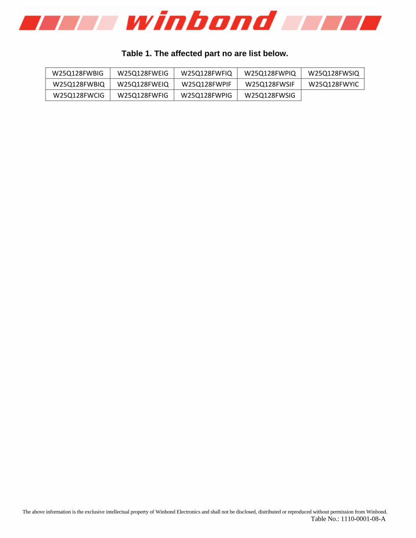
Table 1. The affected part no are list below.
W25Q128FWBIG W25Q128FWEIG W25Q128FWFIQ W25Q128FWPIQ W25Q128FWSIQ
W25Q128FWBIQ W25Q128FWEIQ W25Q128FWPIF W25Q128FWSIF W25Q128FWYIC
W25Q128FWCIG W25Q128FWFIG W25Q128FWPIG W25Q128FWSIG
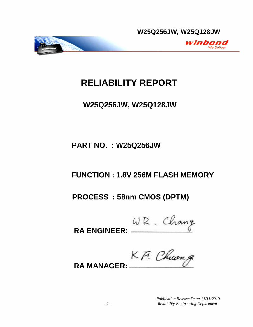
W25Q256JW, W25Q128JW
Publication Release Date: 11/11/2019
-1- Reliability Engineering Department
PART NO. : W25Q256JW
FUNCTION : 1.8V 256M FLASH MEMORY
PROCESS : 58nm CMOS (DPTM)
RA ENGINEER:
RA MANAGER:
RELIABILITY REPORT
W25Q256JW, W25Q128JW

W25Q256JW, W25Q128JW
Publication Release Date: 11/11/2019
- 2 - Reliability Engineering Department
~ INTRODUCTION ~
W25Q256JW and W25Q128JW are a family of 128M-bit through
256M-bit Serial Flash memories fabricated with 58nm process
technology and dual- poly- triple-metal (DPTM) high
performance CMOS process.
According to Winbond`s product family qualification
methodology, the product with lager chip size could be used as
the test vehicle for the product family qualification. Besides,
W25Q256JW and W25Q128JW are manufactured by same
technology. Therefore, we conclude that W25Q256JW and
W25Q128JW do pass product qualification.
W25Q256JW, W25Q128JW
Publication Release Date: 11/11/2019
- 3 - Reliability Engineering Department
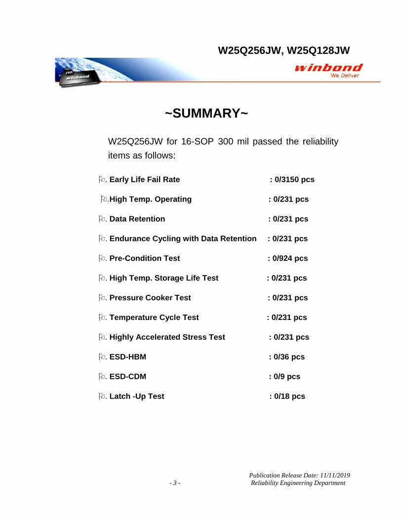
~SUMMARY~
W25Q256JW for 16-SOP 300 mil passed the reliability
items as follows:
. Early Life Fail Rate : 0/3150 pcs
.High Temp. Operating : 0/231 pcs
. Data Retention : 0/231 pcs
. Endurance Cycling with Data Retention : 0/231 pcs
. Pre-Condition Test : 0/924 pcs
. High Temp. Storage Life Test : 0/231 pcs
. Pressure Cooker Test : 0/231 pcs
. Temperature Cycle Test : 0/231 pcs
. Highly Accelerated Stress Test : 0/231 pcs
. ESD-HBM : 0/36 pcs
. ESD-CDM : 0/9 pcs
. Latch -Up Test : 0/18 pcs
W25Q256JW, W25Q128JW
Publication Release Date: 11/11/2019
- 4 - Reliability Engineering Department
---CONTENTS---
Ⅰ. PRODUCT DESCRIPTION
A. Introduction
B. Features
C. Function Block
Ⅱ. LIFE TEST
A. Introduction
1. Early Life Fail Rate (ELFR)
2. High Temp. Operating Life Test (HTOL)
3. Data Retention (DR)
4. Non-Volatile Memory Cycling Endurance (NVCE)
B. Test Results
1. Early Life Fail Rate (ELFR)
2. High Temp. Operating Life Test (HTOL)
3. Data Retention (DR)
4. Non-Volatile Memory Cycling Endurance (NVCE)

W25Q256JW, W25Q128JW
Publication Release Date: 11/11/2019
- 5 - Reliability Engineering Department
Ⅲ. ENVIRONMENTAL TEST
A. Introduction
1. Pre-Condition Test
2. High Temp. Storage Life Test (HTSL)
3. Pressure Cooker Test (PCT)
4. Highly Accelerated Stress Testing (HAST)
5. Temperature Cycle Test (TCT)
B. Test Results
1. Pre-Condition Test
2. High Temp. Storage Life Test (HTSL)
3. Pressure Cooker Test (PCT)
4. Highly Accelerated Stress Testing (HAST)
5. Temperature Cycle Test (TCT)
Ⅳ. ESD & LATCH-UP
A. Introduction
1. ESD
2. LATCH-UP
B. Test Results
1. ESD
2. LATCH-UP

W25Q256JW, W25Q128JW
Publication Release Date: 11/11/2019
- 6 - Reliability Engineering Department
I. PRODUCT DESCRIPTION
A. Introduction
The W25Q256JW (256M-bit) Serial Flash memory provides a storage
solution for systems with limited space, pins and power. The 25Q series
offers flexibility and performance well beyond ordinary Serial Flash
devices. They are ideal for code shadowing to RAM, executing code
directly from Dual/Quad SPI (XIP) and storing voice, text and data. The
device operates on a single 1.7V to 1.95V power supply with current
consumption as low as 1μA for power-down. All devices are offered in
space-saving packages.
The W25Q256JW array is organized into 131,072 programmable pages
of 256-bytes each. Up to 256 bytes can be programmed at a time. Pages
can be erased in groups of 16 (4KB sector erase), groups of 128 (32KB
block erase), groups of 256 (64KB block erase) or the entire chip (chip
erase). The W25Q256JW has 8,192 erasable sectors and 512 erasable
blocks respectively. The small 4KB sectors allow for greater flexibility in
applications that require data and parameter storage.
The W25Q256JW supports the standard Serial Peripheral Interface (SPI),
and a high performance Dual/Quad output as well as Dual/Quad I/O SPI:
Serial Clock, Chip Select, Serial Data I/O0 (DI), I/O1 (DO), I/O2, and I/O3.
SPI clock frequencies of up to 133MHz are supported allowing equivalent
clock rates of 532MHz (133MHz x 4) for Quad I/O when using the SPI
Fast Read Dual/Quad I/O instructions. These transfer rates can
outperform standard Asynchronous 8 and 16-bit Parallel Flash memories.
A Hold pin, Write Protect pin and programmable write protection, with top
or bottom array control, provide further control flexibility. Additionally, the
device supports JEDEC standard manufacturer and device ID and SFDP
Register, a 64-bit Unique Serial Number and three 256-bytes Security
Registers.

W25Q256JW, W25Q128JW
Publication Release Date: 11/11/2019
- 7 - Reliability Engineering Department
B. Features
New Family of SpiFlash Memories
– W25Q256JW: 256M-bit / 32M-byte
– Standard SPI: CLK, /CS, DI, DO
– Dual SPI: CLK, /CS, IO0, IO1
– Quad SPI: CLK, /CS, IO0, IO1, IO2, IO3
– 3 or 4-Byte Addressing Mode
– Software & Hardware Reset
Highest Performance Serial Flash
– 104MHz Standard/Dual SPI clocks
– 133MHz Quad I/O SPI clocks 532MHz equivalent Quad SPI
– 66MB/S Read command bypass transfer rate
– Min. 100K Program-Erase cycles
– More than 20-year data retention
Low Power, Wide Temperature Range
– Single 1.7V to 1.95V supply
– <1μA Power-down (typ.)
– -40°C to +85°C operating range
Flexible Architecture with 4KB sectors
– Uniform Sector/Block Erase (4K/32K/64K-Byte)
– Program 1 to 256 byte per programmable page
– Erase/Program Suspend & Resume
Advanced Security Features
– Software and Hardware Write-Protect
– Power Supply Lock-Down
– Special OTP protection
– Top/Bottom, Complement array protection
– Individual Block/Sector array protection
– 64-Bit Unique ID for each device
W25Q256JW, W25Q128JW
Publication Release Date:11/11/2019
- 7 - Reliability Engineering Department
– Discoverable Parameters (SFDP) Register
– 3X256-Bytes Security Registers with OTP locks
– Volatile & Non-volatile Status Register Bits
Space Efficient Packaging
– 8-pad WSON 6x5-mm / 8x6-mm
– 16-pin SOIC 300-mil (additional /RESET pin)
– 24-ball TFBGA 8x6-mm
– 32-ball WLCSP
– Contact Winbond for KGD and other options
W25Q256JW, W25Q128JW
Publication Release Date:11/11/2019
- 8 - Reliability Engineering Department
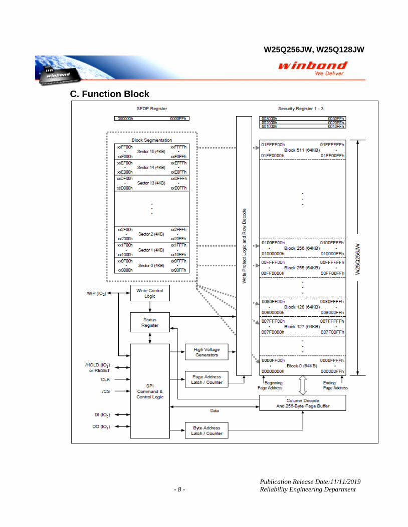
C. Function Block
W25Q256JW, W25Q128JW
Publication Release Date:11/11/2019
- 9 - Reliability Engineering Department
II. LIFE TEST
A. Introduction
1. Early Life Fail Rate (ELFR)
1.1 SCOPE
ELFR test is performed to accelerate infant mortality failure mechanisms
which are thermally activated. This can be achieved by stressing the
devices with bias at high temperature.
1.2 TEST CONDITION
Temp ambient = 125C, Vdd = 1.95V, dynamic stressing, Td = 168 hrs.
(JEDEC74)
2. High-Temperature Operating Life Test (HTOL)
2.1 SCOPE
HTOL test is performed to accelerate failure mechanisms which are
thermally activated. This can be achieved by stressing the devices
with bias at high temperature.
2.2 TEST CONDITION
Temp ambient = 125C, Vdd = 1.95V, dynamic stressing, Td = 1000 hrs.
(JESD22-A108)
3. Data Retention Test (DR)
3.1 SCOPE
DR test is to determine the stability of data stored in the device under
high temperature environment.
3.2 TEST CONDITION
Temp = 150C, Td = 1000 hrs. (JESD22-A117)

W25Q256JW, W25Q128JW
Publication Release Date:11/11/2019
- 10 - Reliability Engineering Department
4. Non-Volatile Memory Cycling Endurance (NVCE)
4.1 SCOPE
Test product’s capability to the number of Program and Erase.
4.2 TEST CONDITION
JEDEC-STD-JESD 47
Room Temp cycling test:
TD (Duration) = 1K, 10K, 100K cycles
Vcc = 1.95V
Pattern = 00, FF, CHKBD
Low temp data retention (LTDR):
Dynamic operation life test at room temp.
TD (Duration) = 500 hrs
Vcc = 1.95V
Apply dynamic pattern.
85℃ cycling test:
TD (Duration) = 1K, 10K, 100K cycles
Vcc = 1.95V
Pattern = 00, FF, CHKBD
High temp data retention (HTDR):
Bake at 125°C
TD (Duration) = 10 hrs for 100K cycling,
100 hrs for 10K and 1K cycling.
W25Q256JW, W25Q128JW
Publication Release Date:11/11/2019
- 11 - Reliability Engineering Department
B. Test Results
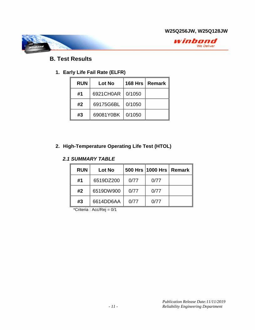
1. Early Life Fail Rate (ELFR)
RUN Lot No 168 Hrs Remark
#1 6921CH0AR 0/1050
#2 69175G6BL 0/1050
#3 69081Y0BK 0/1050
2. High-Temperature Operating Life Test (HTOL)
2.1 SUMMARY TABLE
RUN Lot No 500 Hrs 1000 Hrs Remark
#1 6519DZ200 0/77 0/77
#2 6519DW900 0/77 0/77
#3 6614DD6AA 0/77 0/77
*Criteria : Acc/Rej = 0/1
W25Q256JW, W25Q128JW
Publication Release Date:11/11/2019
- 12 - Reliability Engineering Department
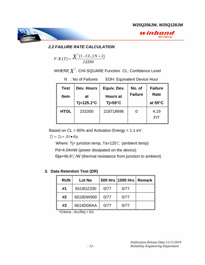
2.2 FAILURE RATE CALCULATION
F R TCL N
EDH
X. .( )( , )
21 2 2
2
WHERE2
X : CHI-SQUARE Function CL: Confidence Level
N : No of Failures EDH: Equivalent Device Hour
Test
Item
Dev. Hours
at
Tj=125.1C
Equiv. Dev.
Hours at
Tj=55C
No. of
Failure
Failure
Rate
at 55C
HTOL 231000 218718696 0
4.19
FIT
Based on CL = 60% and Activation Energy = 1.1 eV
Tj Ta Pd ja
Where: Tj= junction temp, Ta=125℃ (ambient temp)
Pd=4.04mW (power dissipated on the device)
Θja=46.9℃/W (thermal resistance from junction to ambient)
3. Data Retention Test (DR)
RUN Lot No 500 Hrs 1000 Hrs Remark
#1 6519DZ200 0/77 0/77
#2 6519DW900 0/77 0/77
#3 6614DD6AA 0/77 0/77
*Criteria : Acc/Rej = 0/1.
W25Q256JW, W25Q128JW
Publication Release Date:11/11/2019
- 13 - Reliability Engineering Department
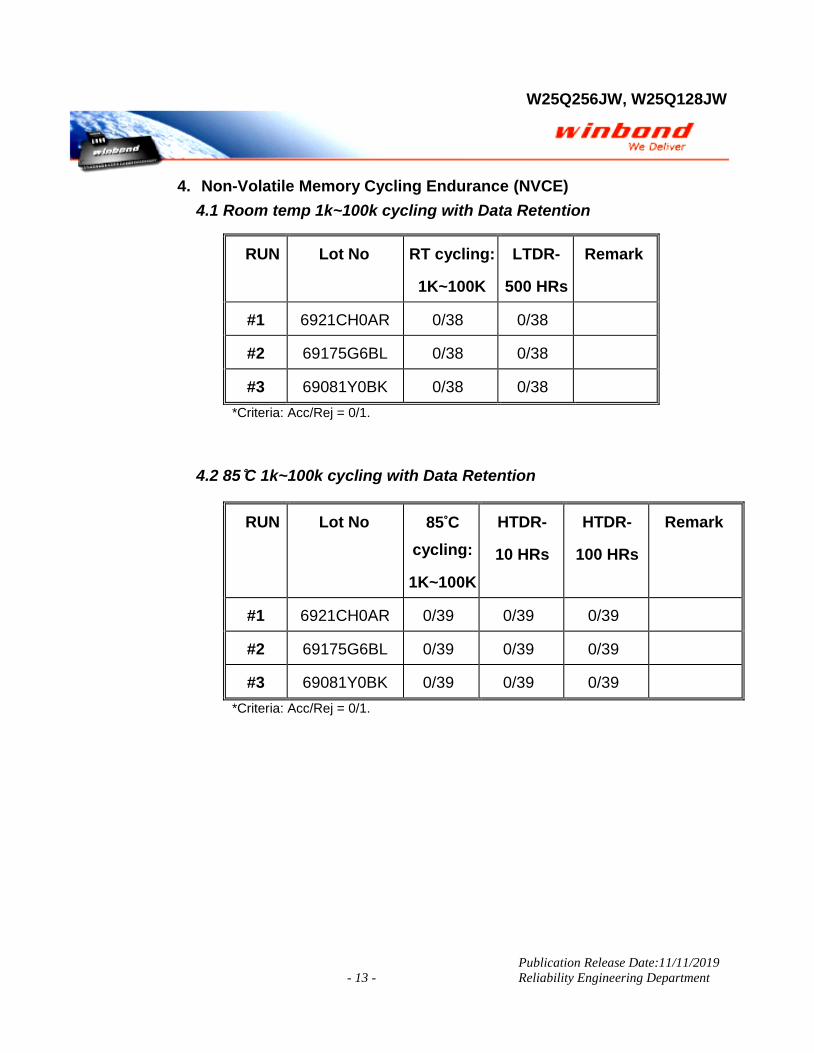
4. Non-Volatile Memory Cycling Endurance (NVCE)
4.1 Room temp 1k~100k cycling with Data Retention
RUN Lot No RT cycling:
1K~100K
LTDR-
500 HRs
Remark
#1 6921CH0AR 0/38 0/38
#2 69175G6BL 0/38 0/38
#3 69081Y0BK 0/38 0/38
*Criteria: Acc/Rej = 0/1.
4.2 85°C 1k~100k cycling with Data Retention
RUN Lot No 85°C
cycling:
1K~100K
HTDR-
10 HRs
HTDR-
100 HRs
Remark
#1 6921CH0AR 0/39 0/39 0/39
#2 69175G6BL 0/39 0/39 0/39
#3 69081Y0BK 0/39 0/39 0/39
*Criteria: Acc/Rej = 0/1.
W25Q256JW, W25Q128JW
Publication Release Date:11/11/2019
- 14 - Reliability Engineering Department
III. ENVIRONMENTAL TESTS
A. Introduction
1. Pre-condition Test
1.1 SCOPE
Pre-condition Test is to measure the resistance of SMD (Surface Mount
Devices) to the storage environment at the customer site and to thermal
stress created by IR reflow.
1.2 TEST CONDITION
Step 1: TCT (-65C/150C, 5 cycles)
Step 2: Bake (125C, 24 hours)
Step 3: Soak (60C/60%RH, 52 hours)
Step 4: IR, 3 passes (JEDEC 020).
2. High Temperature Storage Life Test (HTSL)
2.1 SCOPE
HTSL test is to determine the stability of the device in high temperature
environment.
2.2 TEST CONDITION
Temp = 150C, Td = 1000 hrs. (JESD22-A103)
3. Pressure Cooker Test (PCT)
3.1 SCOPE
PCT is to evaluate the device resistance to moisture penetration.
3.2 TEST CONDITION
Ta = 121C, RH = 100%, P = 2 atm, Td = 168 Hrs. (JESD22-A102)
W25Q256JW, W25Q128JW
Publication Release Date:11/11/2019
- 15 - Reliability Engineering Department
4. Highly Accelerated Stress Testing (HAST)
4.1 SCOPE
HAST is to evaluate the reliability of non hermetic packaged solid-state
device in humid environments.
4.2 TEST CONDITION
Ta = 130C, Vdd=1.95V, RH% = 85%, Td = 168 Hrs. (JESD22-A110)
5. Temperature Cycle Test (TCT)
5.1 SCOPE
TCT is to evaluate the resistance of device to environmental temperature
change.
5.2 TEST CONDITION
-65C ~ +150 C, Condition C, Soak Mode 1, 500 cycles.
(JESD22-A104)
W25Q256JW, W25Q128JW
Publication Release Date:11/11/2019
- 16 - Reliability Engineering Department
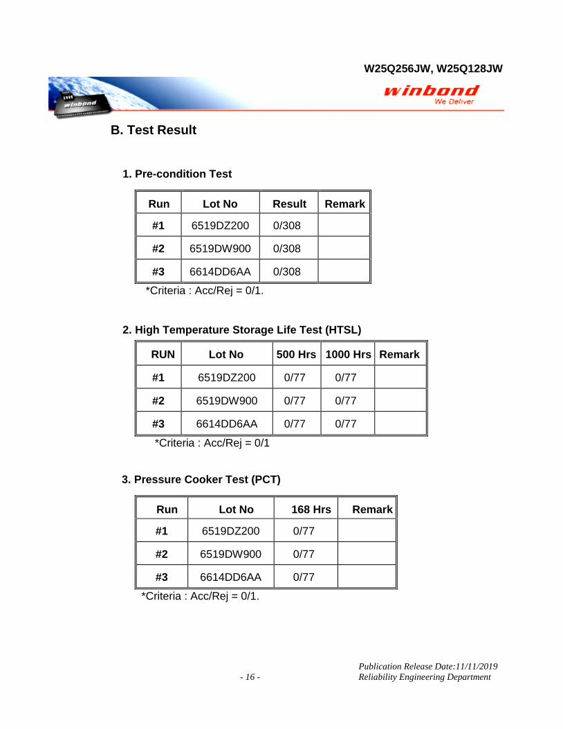
B. Test Result
1. Pre-condition Test
Run Lot No Result Remark
#1 6519DZ200 0/308
#2 6519DW900 0/308
#3 6614DD6AA 0/308
*Criteria : Acc/Rej = 0/1.
2. High Temperature Storage Life Test (HTSL)
RUN Lot No 500 Hrs 1000 Hrs Remark
#1 6519DZ200 0/77 0/77
#2 6519DW900 0/77 0/77
#3 6614DD6AA 0/77 0/77
*Criteria : Acc/Rej = 0/1
3. Pressure Cooker Test (PCT)
Run Lot No 168 Hrs Remark
#1 6519DZ200 0/77
#2 6519DW900 0/77
#3 6614DD6AA 0/77
*Criteria : Acc/Rej = 0/1.
W25Q256JW, W25Q128JW
Publication Release Date:11/11/2019
- 17 - Reliability Engineering Department
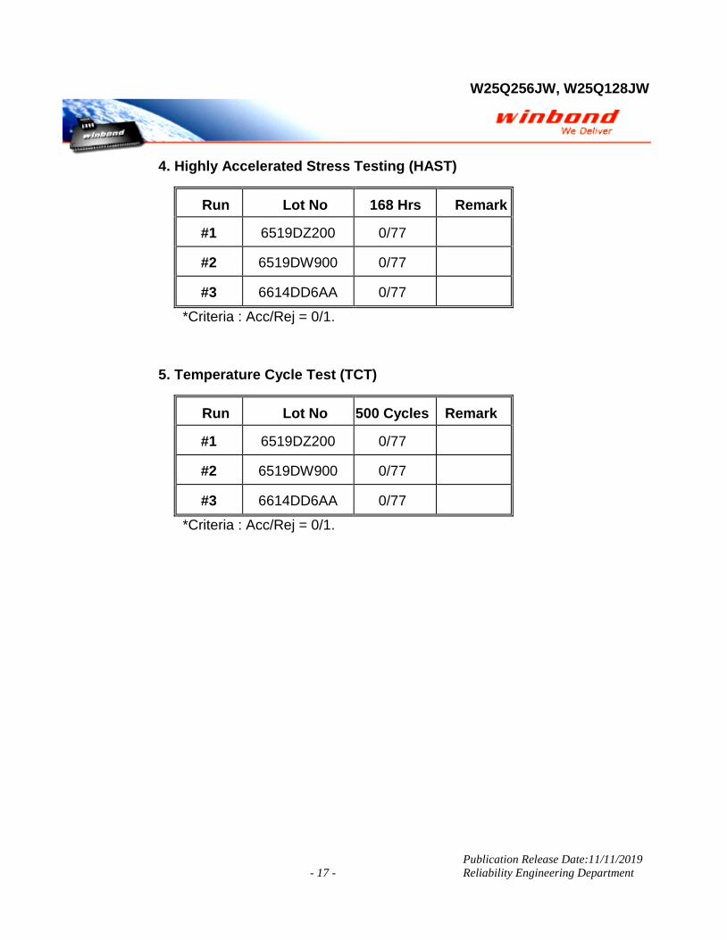
4. Highly Accelerated Stress Testing (HAST)
Run Lot No 168 Hrs Remark
#1 6519DZ200 0/77
#2 6519DW900 0/77
#3 6614DD6AA 0/77
*Criteria : Acc/Rej = 0/1.
5. Temperature Cycle Test (TCT)
Run Lot No 500 Cycles Remark
#1 6519DZ200 0/77
#2 6519DW900 0/77
#3 6614DD6AA 0/77
*Criteria : Acc/Rej = 0/1.
W25Q256JW, W25Q128JW
Publication Release Date:11/11/2019
- 18 - Reliability Engineering Department
IV. ESD AND LATCH-UP
A. Introduction
1. ESD
1.1 SCOPE
ESD test is to evaluate the immunity of device to electrostatic
discharge.
1.2 TEST CONDITION
Human Body Model (HBM): JS-001
Charge Device Model (CDM): JS-002
2. Latch-Up
2.1 SCOPE
Latch-Up test is to evaluate the immunity of the devices to latch-up.
2.2 TEST CONDITION
JEDEC STD 78E, Temp = 25 C, VDD = Max. Operating Voltage
W25Q256JW, W25Q128JW
Publication Release Date:11/11/2019
- 19 - Reliability Engineering Department
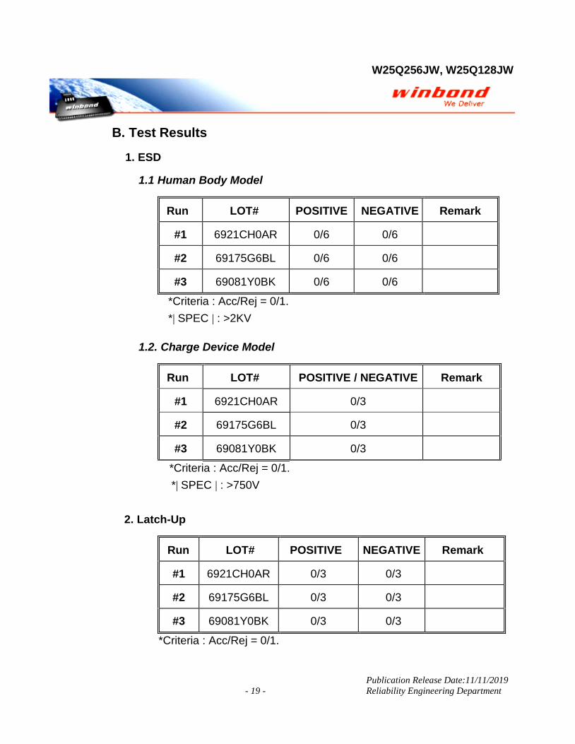
B. Test Results
1. ESD
1.1 Human Body Model
Run LOT# POSITIVE NEGATIVE Remark
#1 6921CH0AR 0/6 0/6
#2 69175G6BL 0/6 0/6
#3 69081Y0BK 0/6 0/6
*Criteria : Acc/Rej = 0/1.
*| SPEC | : >2KV
1.2. Charge Device Model
Run LOT# POSITIVE / NEGATIVE Remark
#1 6921CH0AR 0/3
#2 69175G6BL 0/3
#3 69081Y0BK 0/3
*Criteria : Acc/Rej = 0/1.
*| SPEC | : >750V
2. Latch-Up
Run LOT# POSITIVE NEGATIVE Remark
#1 6921CH0AR 0/3 0/3
#2 69175G6BL 0/3 0/3
#3 69081Y0BK 0/3 0/3
*Criteria : Acc/Rej = 0/1.
W25Q256JW, W25Q128JW
Publication Release Date:11/11/2019
- 20 - Reliability Engineering Department
*| SPEC. | : I-Test > 200mA
Vsupply over voltage Test>1.5x max supply voltage
W25Q256JW, W25Q128JW
Publication Release Date:11/11/2019
- 21 - Reliability Engineering Department

Hazardous Substances Check List
Raw material name: W25Q128JWPIQ
Element Specification Measured Data DL Result
Cd (Cadmium, 鎘鎘鎘鎘)
< 20ppm ND 0.8 PASS
Pb (Lead, 鉛鉛鉛鉛)
< 700ppm 1 ppm 0.4 PASS
Hg (Mercury, 汞汞汞汞)
< 200ppm ND 0.4 PASS
Cr (Chromium, 鉻鉻鉻鉻)
< 700ppm 3 ppm 0.8 PASS
Br (Bromine, 溴溴溴溴)
< 250ppm 10 ppm 0.1 PASS
Cl (Chlorine, 氯氯氯氯)
< 630ppm ND 15 PASS
Sb (Antimony, 銻銻銻銻)
< 700ppm ND 2.5 PASS 註註註註: DL 為儀器之有效偵測極限為儀器之有效偵測極限為儀器之有效偵測極限為儀器之有效偵測極限,,,,量測值量測值量測值量測值 < DL,,,,則標示則標示則標示則標示 ND。。。。
Conclusion: ■■■■ Accept ���� Reject
Engineer:
Date: 2019/11/26

Hazardous Substances Check List
Raw material name: W25Q128JWYIQ
Element Specification Measured Data DL Result
Cd (Cadmium, 鎘鎘鎘鎘)
< 20ppm ND 0.8 PASS
Pb (Lead, 鉛鉛鉛鉛)
< 700ppm 7 ppm 0.4 PASS
Hg (Mercury, 汞汞汞汞)
< 200ppm ND 0.4 PASS
Cr (Chromium, 鉻鉻鉻鉻)
< 700ppm 103 ppm 0.8 PASS
Br (Bromine, 溴溴溴溴)
< 250ppm ND 0.1 PASS
Cl (Chlorine, 氯氯氯氯)
< 630ppm ND 15 PASS
Sb (Antimony, 銻銻銻銻)
< 700ppm ND 2.5 PASS 註註註註: DL 為儀器之有效偵測極限為儀器之有效偵測極限為儀器之有效偵測極限為儀器之有效偵測極限,,,,量測值量測值量測值量測值 < DL,,,,則標示則標示則標示則標示 ND。。。。
Conclusion: ■■■■ Accept ���� Reject
Engineer:
Date: 2019/11/26
Hazardous Substances Check List
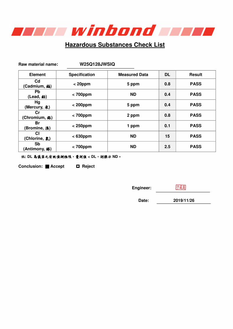
Raw material name: W25Q128JWSIQ
Element Specification Measured Data DL Result
Cd (Cadmium, 鎘鎘鎘鎘)
< 20ppm 5 ppm 0.8 PASS
Pb (Lead, 鉛鉛鉛鉛)
< 700ppm ND 0.4 PASS
Hg (Mercury, 汞汞汞汞)
< 200ppm 5 ppm 0.4 PASS
Cr (Chromium, 鉻鉻鉻鉻)
< 700ppm 2 ppm 0.8 PASS
Br (Bromine, 溴溴溴溴)
< 250ppm 1 ppm 0.1 PASS
Cl (Chlorine, 氯氯氯氯)
< 630ppm ND 15 PASS
Sb (Antimony, 銻銻銻銻)
< 700ppm ND 2.5 PASS 註註註註: DL 為儀器之有效偵測極限為儀器之有效偵測極限為儀器之有效偵測極限為儀器之有效偵測極限,,,,量測值量測值量測值量測值 < DL,,,,則標示則標示則標示則標示 ND。。。。
Conclusion: ■■■■ Accept ���� Reject
Engineer:
Date: 2019/11/26
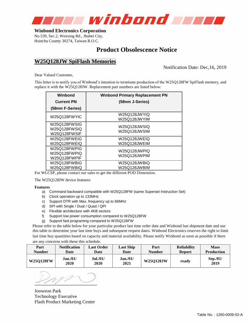
Table No. : 1260-0009-02-A
Winbond Electronics Corporation No.539, Sec.2, Wenxing Rd., Jhubei City,
Hsinchu County 30274, Taiwan R.O.C.
Product Obsolescence Notice
W25Q128JW SpiFlash Memories
Notification Date: Dec,16, 2019
Dear Valued Customer,
This letter is to notify you of Winbond’s intention to terminate production of the W25Q128FW SpiFlash memory, and
replace it with the W25Q128JW. Replacement part numbers are listed below:
Winbond Winbond Primary Replacement PN
Current PN (58nm J-Series)
(58nm F-Series)
W25Q128FWYIC W25Q128JWYIQ W25Q128JWYIM
W25Q128FWSIG W25Q128FWSIQ W25Q128FWSIF
W25Q128JWSIQ W25Q128JWSIM
W25Q128FWEIG W25Q128FWEIQ
W25Q128JWEIQ W25Q128JWEIM
W25Q128FWPIG W25Q128FWPIQ W25Q128FWPIF
W25Q128JWPIQ W25Q128JWPIM
W25Q128FWBIG W25Q128FWBIQ
W25Q128JWBIQ W25Q128JWBIM
For WLCSP, please contact our sales to get the different POD Dimension.
The W25Q128JW device features:
Features a) Command backward compatible with W25Q128FW (same Superset Instruction Set)
b) Clock operation up to 133MHz
c) Support DTR with Max. frequency up to 66MHz
d) SPI with Single / Dual / Quad / QPI
e) Flexible architecture with 4KB sectors
f) Support low power consumption compared to W25Q128FW
g) Support fast programing compared to W25Q128FW
Please refer to the table below for your particular product last time order date and Winbond last shipment date and use
this table to determine your last time buys and subsequent request dates. Winbond Electronics reserves the right to limit
last time buy quantities based on capacity and material availability. Please notify Winbond as soon as possible if there
are any concerns with these this schedule.
Part
Number
Notification
Date
Last Order
Date
Last Ship
Date
Part
Number
Reliability
Report
Mass
Production
W25Q128FW Jan./01/
2020
Jul./01/
2020
Jan./01/
2021 W25Q128JW ready
Sep./01/
2019
Jooweon Park
Technology Executive
Flash Product Marketing Center
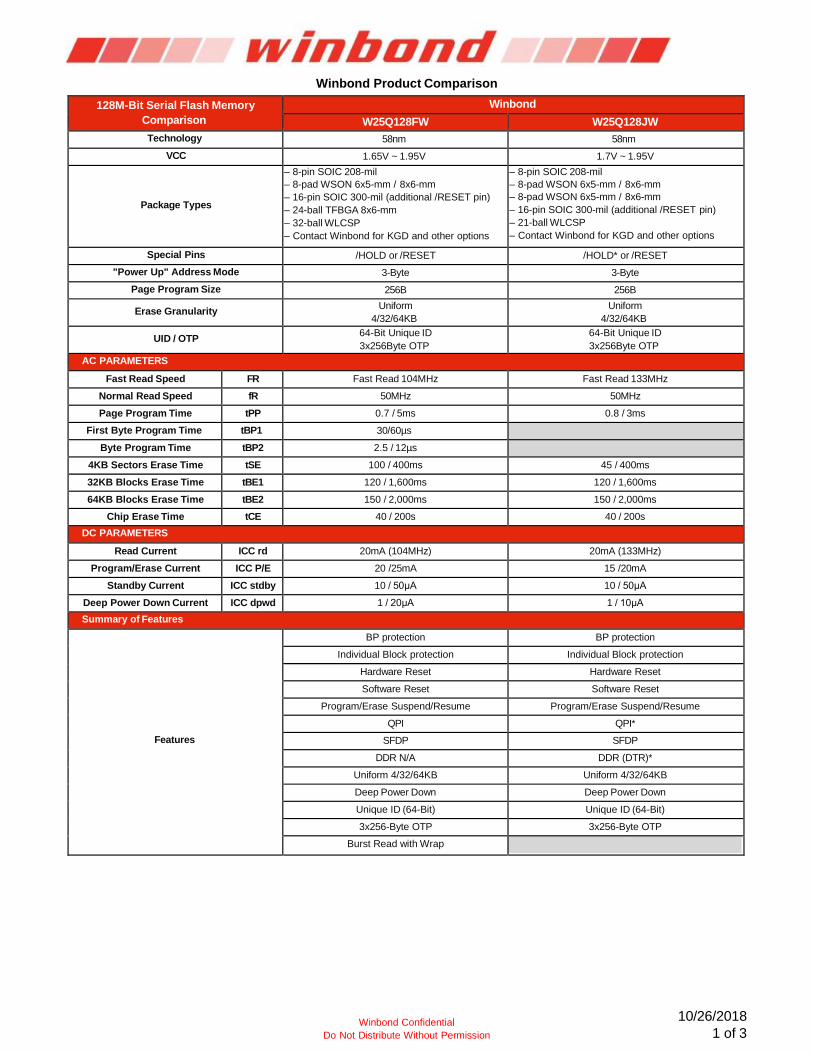
Winbond Product Comparison
128M-Bit Serial Flash Memory Comparison
Winbond W25Q128FW W25Q128JW
Technology 58nm 58nm VCC 1.65V ~ 1.95V 1.7V ~ 1.95V
Package Types
– 8-pin SOIC 208-mil – 8-pad WSON 6x5-mm / 8x6-mm – 16-pin SOIC 300-mil (additional /RESET pin)
– 24-ball TFBGA 8x6-mm – 32-ball WLCSP – Contact Winbond for KGD and other options
– 8-pin SOIC 208-mil – 8-pad WSON 6x5-mm / 8x6-mm
– 8-pad WSON 6x5-mm / 8x6-mm
– 16-pin SOIC 300-mil (additional /RESET pin) – 21-ball WLCSP – Contact Winbond for KGD and other options
Special Pins /HOLD or /RESET /HOLD* or /RESET "Power Up" Address Mode 3-Byte 3-Byte
Page Program Size 256B 256B
Erase Granularity Uniform 4/32/64KB
Uniform 4/32/64KB
UID / OTP 64-Bit Unique ID
3x256Byte OTP 64-Bit Unique ID 3x256Byte OTP
AC PARAMETERS Fast Read Speed FR Fast Read 104MHz Fast Read 133MHz
Normal Read Speed fR 50MHz 50MHz Page Program Time tPP 0.7 / 5ms 0.8 / 3ms
First Byte Program Time tBP1 30/60µs Byte Program Time tBP2 2.5 / 12µs
4KB Sectors Erase Time tSE 100 / 400ms 45 / 400ms 32KB Blocks Erase Time tBE1 120 / 1,600ms 120 / 1,600ms 64KB Blocks Erase Time tBE2 150 / 2,000ms 150 / 2,000ms
Chip Erase Time tCE 40 / 200s 40 / 200s DC PARAMETERS
Read Current ICC rd 20mA (104MHz) 20mA (133MHz) Program/Erase Current ICC P/E 20 /25mA 15 /20mA
Standby Current ICC stdby 10 / 50μA 10 / 50μA Deep Power Down Current ICC dpwd 1 / 20μA 1 / 10μA Summary of Features
Features
BP protection BP protection Individual Block protection Individual Block protection
Hardware Reset Hardware Reset Software Reset Software Reset
Program/Erase Suspend/Resume Program/Erase Suspend/Resume QPI QPI*
SFDP SFDP DDR N/A DDR (DTR)*
Uniform 4/32/64KB Uniform 4/32/64KB Deep Power Down Deep Power Down Unique ID (64-Bit) Unique ID (64-Bit) 3x256-Byte OTP 3x256-Byte OTP
Burst Read with Wrap
Winbond Confidential Do Not Distribute Without Permission
10/26/2018 1 of 3
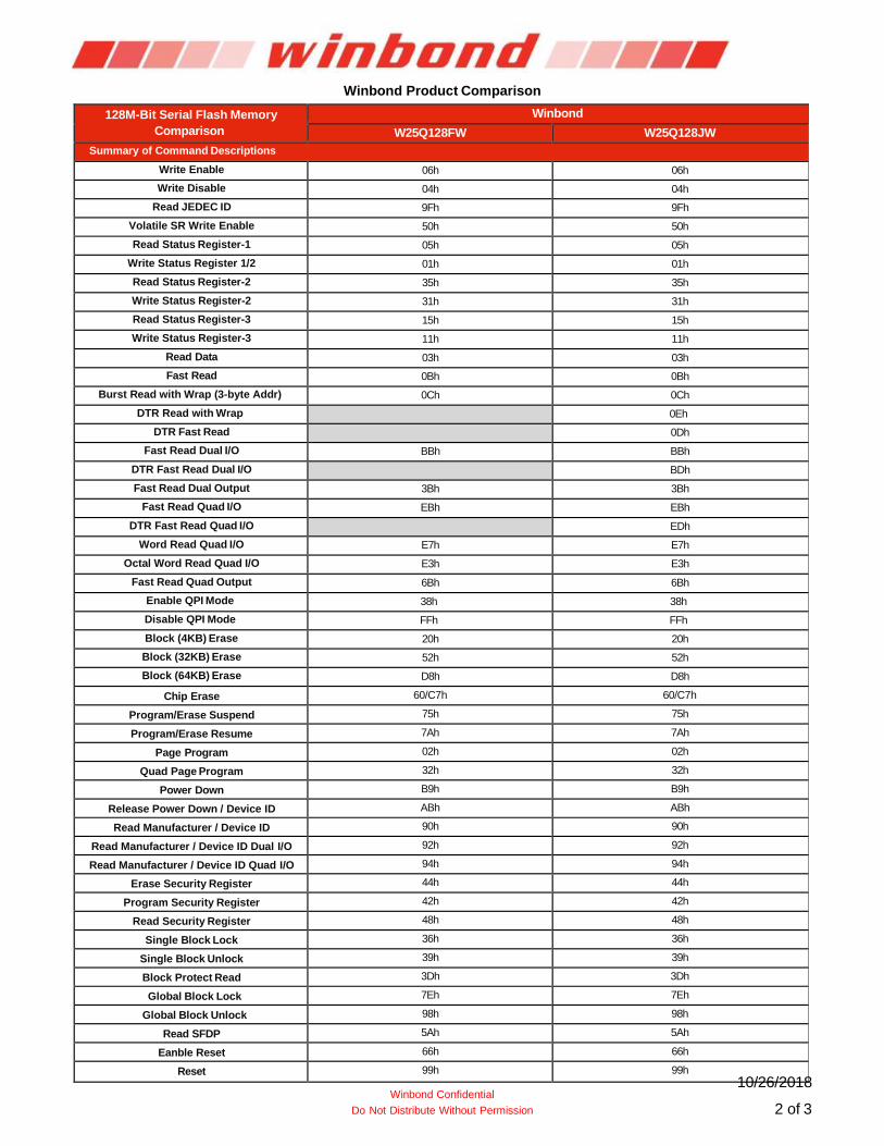
Winbond Product Comparison
10/26/2018 Winbond Confidential
Do Not Distribute Without Permission 2 of 3
128M-Bit Serial Flash Memory Comparison
Winbond W25Q128FW W25Q128JW
Summary of Command Descriptions Write Enable 06h 06h Write Disable 04h 04h
Read JEDEC ID 9Fh 9Fh Volatile SR Write Enable 50h 50h Read Status Register-1 05h 05h
Write Status Register 1/2 01h 01h Read Status Register-2 35h 35h Write Status Register-2 31h 31h Read Status Register-3 15h 15h Write Status Register-3 11h 11h
Read Data 03h 03h Fast Read 0Bh 0Bh
Burst Read with Wrap (3-byte Addr) 0Ch 0Ch DTR Read with Wrap 0Eh
DTR Fast Read 0Dh Fast Read Dual I/O BBh BBh
DTR Fast Read Dual I/O BDh Fast Read Dual Output 3Bh 3Bh
Fast Read Quad I/O EBh EBh DTR Fast Read Quad I/O EDh
Word Read Quad I/O E7h E7h Octal Word Read Quad I/O E3h E3h
Fast Read Quad Output 6Bh 6Bh Enable QPI Mode 38h 38h Disable QPI Mode FFh FFh Block (4KB) Erase 20h 20h Block (32KB) Erase 52h 52h Block (64KB) Erase D8h D8h
Chip Erase 60/C7h 60/C7h Program/Erase Suspend 75h 75h Program/Erase Resume 7Ah 7Ah
Page Program 02h 02h Quad Page Program 32h 32h
Power Down B9h B9h Release Power Down / Device ID ABh ABh Read Manufacturer / Device ID 90h 90h
Read Manufacturer / Device ID Dual I/O 92h 92h Read Manufacturer / Device ID Quad I/O 94h 94h
Erase Security Register 44h 44h Program Security Register 42h 42h
Read Security Register 48h 48h Single Block Lock 36h 36h
Single Block Unlock 39h 39h Block Protect Read 3Dh 3Dh Global Block Lock 7Eh 7Eh
Global Block Unlock 98h 98h Read SFDP 5Ah 5Ah
Eanble Reset 66h 66h Reset 99h 99h
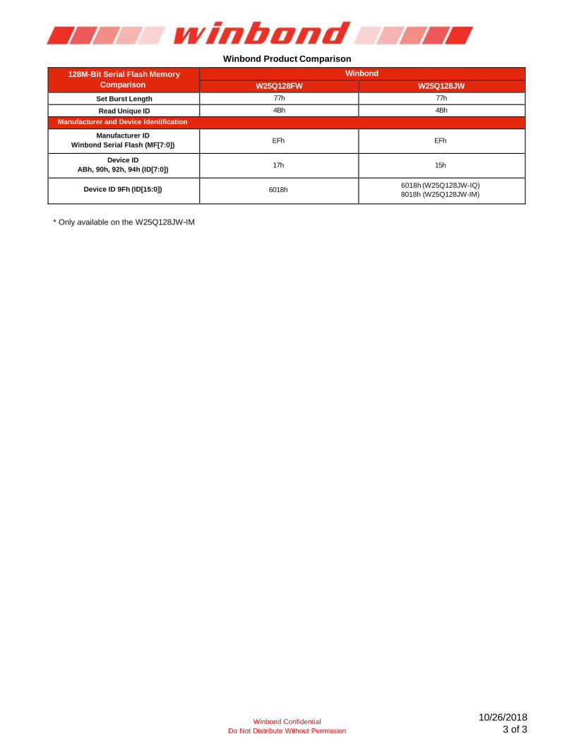
Winbond Product Comparison
128M-Bit Serial Flash Memory Comparison
Winbond W25Q128FW W25Q128JW
Set Burst Length 77h 77h Read Unique ID 4Bh 4Bh
Manufacturer and Device Identification Manufacturer ID
Winbond Serial Flash (MF[7:0])
EFh
EFh
Device ID ABh, 90h, 92h, 94h (ID[7:0])
17h
15h
Device ID 9Fh (ID[15:0])
6018h 6018h (W25Q128JW-IQ)
8018h (W25Q128JW-IM)
* Only available on the W25Q128JW-IM
Winbond Confidential Do Not Distribute Without Permission
10/26/2018 3 of 3
11/04/2019
W25Q128FW and W25Q128JW
WLCSP POD comparison
PH20 Marten
Dec./2019
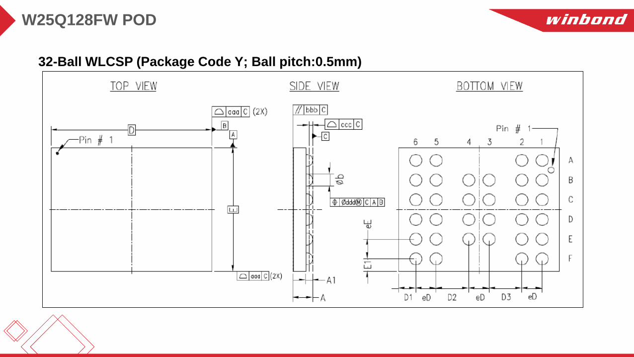
W25Q128FW POD
32-Ball WLCSP (Package Code Y; Ball pitch:0.5mm)
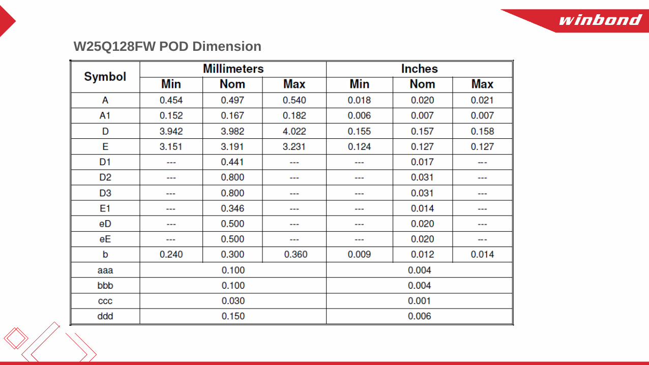
W25Q128FW POD Dimension

W25Q128JW POD
21-Ball WLCSP (Package Code Y, Ball pitch:0.5mm)
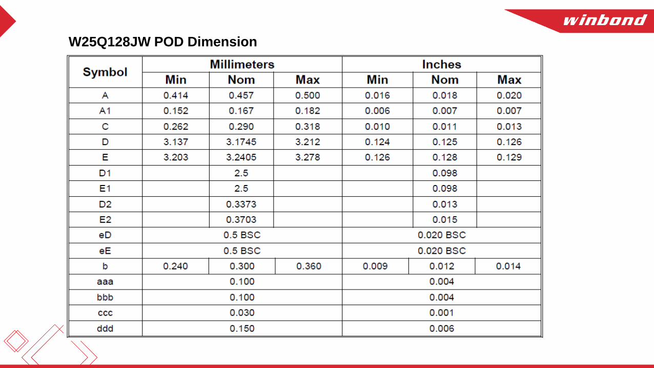
W25Q128JW POD Dimension

Thank Youwww.winbond.com
Website