process improvements for ultra-thick photoresist using a
TRANSCRIPT

Flack, Nguyen and Capsuto 1
SPIE 2001 #4346-97
Process Improvements for Ultra-Thick Photoresist Using a Broadband Stepper
Warren W. Flack, Ha-Ai NguyenUltratech Stepper, Inc. San Jose, CA 95134
Elliott CapsutoShinEtsuMicroSi, Inc.San Jose, CA 95112
There are a number of new lithographic applications that require the use of ultra-thick photoresists. Extremelylarge structure heights and high aspect ratios are often necessary for electroplating processes. In this situation it isimportant for the height of the patterned photoresist to exceed the plating height. Two of the main applications forthick photoresist are micromachining and advanced packaging. Ultra-thick photoresists are used in packaging todefine the size and location of the bonds for bump bonding, while in micromachining the photoresist is used todefine fluidic chambers and electroforming molds.
At photoresist thickness greater than 15 microns, standard lithographic techniques become difficult in terms ofperformance and productivity. The bake, exposure and develop times increase dramatically as the photoresistthickness climbs. The estimated total process time for a 15 micron photoresist is approximately three timesgreater than that of a 1 micron photoresist. For thick films the develop time on the wafer track becomes thethroughput limiter for the entire lithography cell. Therefore, reducing develop time for thick photoresist processesis critical to enhancing the lithography cell cost of ownership.
In this paper we will focus on the developer chemistry and process to improve both performance and productivityfor a 15 micron thick photoresist. We evaluate process changes in both normality and surfactant level of thedeveloper. Cross sectional analysis, contrast curves, process linearity and process windows are used to establishthe lithographic capabilities. It is clear that a developer and process for a thin photoresist is not necessarilyoptimum for a thick photoresist process. The implementation of an ultra-thick photoresist becomes more feasiblein a manufacturing environment after optimizing developer chemistry and process conditions.
Key Words: thick photoresist, developer, surfactant, normality, photoresist characterization, broadband stepper,productivity, advanced packaging, MEMS, plating
1.0 INTRODUCTION
Rapid growth is being experienced today in the areas of micro-mechanical systems (MEMS) and advancedpackaging [1,2,3,4,5]. Additionally there have been very rapid technology changes in the magnetic headrecording industry. All three of these market segments utilize thick photosensitive materials for electroplating.The largest upcoming market segment is wafer level packaging. The semiconductor manufacturing industry isconverting to wafer level packaging to reduce cost and increase performance by replacing single chip wirebonding with bump bonding applications as the final step in chip manufacturing. Extending the microlithographic

Flack, Nguyen and Capsuto 2
SPIE 2001 #4346-97
processes into these rapidly growing areas is placing new demands on both the photosensitive materials and thelithography equipment.
Electroplating metals for micro-scale features itself does not present new technical challenges. However, thefabrication of high aspect ratio linewidths for these applications is a new and challenging use of photolithographyequipment and photoresists. The photolithography requirements for thick photoresists can be addressed by usingoptical lithography equipment originally developed for production of semiconductor devices. Steppers, full waferscanners and contact printers are widely used in the microelectronic industry and are highly evolved productiontools. Thick photoresists, however, typically require a high exposure dosage and large depth of focus (DOF) forhigh aspect ratio lithography of larger geometries. For these reasons, it is advantageous to utilize a stepper with abroad band exposure system and low numerical aperture (NA) to maximize the illumination intensity at the waferplane and to improve DOF.
Photoresist performance, like stepper performance, has generally been optimized over recent years for achievingthe smallest geometries possible. Some newer photoresist formulations are available that have properties moretailored for making the high aspect ratio structures required for electroplating molds. The process operatingconditions for thick photoresists are considerably different than for thin photoresists. In the case of thinphotoresists the two issues are resolution and latitude [6]. With thick films the concerns are centered aroundaspect ratios, downstream plating performance, latitudes and productivity. As spin coated photoresist filmsbecome more popular for these applications, it becomes important to study thick photoresists for optimization ofperformance and productivity [7,8,9,10].
The cost of ownership of a lithography cell is driven primarily by the cost of the individual equipment and theeffective throughput of the cell. Traditionally the exposure time is the limiting factor since the exposure system isthe most expensive part of the cell. However, with thick photoresist films the track developer process can be thelimiting factor with develop time in excess of 5 minutes. By improving the develop rate, the total exposure anddevelop time will decrease, reducing the total cost of ownership. This can be achieved by increasing thedeveloper normality and optimizing the level of surfactant. However, simply changing develop conditions canimpact the photoresist performance including critical dimension (CD) control, profile and aspect ratios.
Standard normality developer at 0.26N is used in the semiconductor industry for balancing photoresistperformance and throughput. Since many thick photoresist applications don’t have as challenging of a CDrequirement, it is possible that higher normality developers will be acceptable. The objective of this study is tofind a faster photoresist/developer system (normality and surfactant) at the same time maintaining a processacceptable for thick photoresist applications.
2.0 EXPERIMENTAL METHODS
2.1 Lithography Equipment
Lithography for the thick photoresist evaluated in this study was performed on an Ultratech Stepper SaturnSpectrum 3 Wafer Stepper®. The optical specifications for the Saturn Spectrum 3 are shown in Table 1. TheSaturn Spectrum 3 stepper is based on the 1X Wynne-Dyson lens design employing Mercury (Hg) g, h and i-lineillumination from 350 to 450 nm and having a 0.16 NA [11]. Broadband exposure is possible due to the uniquedesign characteristics of the Wynne Dyson lens system. This symmetric catadioptric lens system does notintroduce the chromatic aberrations common to other lens systems when broadband illumination is used. The lowNA and broadband illumination spectrum of the Saturn Spectrum 3 provides a more uniform aerial image through

Flack, Nguyen and Capsuto 3
SPIE 2001 #4346-97
the depth of the ultrathick photosensitive materials in contrast to steppers with larger NAs and a relatively narrowbandwidth.
A filter system was employed which allows ghi-line (350 to 450 nm), gh-line (390 to 450 nm) or i-line (355 to375 nm) illumination to be selected. This approach can be used to optimize lithographic performance based onthe spectral sensitivity of the photosensitive material.
Multiple wafers were exposed in a focus/exposure pattern consisting of a nine by nine field array as illustrated inFigure 1. Nominal exposure times were determined by measuring isolated space patterns at the specific linewidthof interest with a KLA-Tencor 8100 metrology SEM. A zero percent threshold criteria was selected for thedetermination of the CD.
The Ultratech 1X reticle used for this study was designed primarily to support easy cross sectional SEMmetrology for micromachining applications. The reticle consists of two fields of 10 mm by 10 mm, one of eachpolarity to support both positive and negative acting photoresists. Each field contains horizontal and verticalgrouped line and space patterns from 0.5 to 50 µm. Both equal line and space patterns and isolated lines areincluded for all structure sizes. For each structure size the center line or space extends to create an isolatedfeature. All of the line structures are 7 mm in length to facilitate cross sectional SEM analysis. There was no databiasing applied to the design data and CDs were held to within ±0.03 µm of a nominal chrome line. Reticle CDinformation was also obtained for all line sizes on both fields to establish the process linearity in reticlefabrication.
2.2 Photoresist Processing
SEMI standard ultra-flat silicon wafers were used for this study. The 150 mm wafers were pre-treated accordingto recommendations by ShinEtsuMicroSi as described in Table 2. The ultra-thick photoresist used for thisinvestigation was ShinEtsu SIPR® 9270M-12.0 positive photoresist. The photoresist coats to a nominal thicknessof 12 µm at 3000 rpm. The ShinEtsu SIPR 9270M was coated to the 15 µm target thickness using the process andequipment described in Table 2. Photoresist thickness and uniformity were measured on a Nanometric 8300Xmeasurement system.
ShinEtsu SIPR 9270M photoresist utilizes a bonded sensitizer to the novolak resin. Built into the PAC (photoactive component) is a diazo group that pseudo-crosslinks when exposed to the OH- groups of the organictetramethylammonium hydroxide (TMAH) developer. Effectively the dissolution rate of the photoresist decreasesas the exposure to OH- increases. This is a valuable mechanism for thick photoresist application by decreasingunexposed photoresist loss and improving photoresist profiles at the top of the film stack where the exposure todeveloper can be on the order of 3 to 5 minutes depending on the photoresist thickness. The 3 to 5 minutes ofdevelop time at the top of the resist is of great contrast to the bottom of the profile where the exposure todeveloper can be much less than one minute.
The developer used was Moses Lake 0.26N, 0.30N and 0.35N with two levels of surfactant. Moses Lake preparedthe developer samples in order to facilitate the experiments. The lower level of surfactant had a surface tension of43 dyne/cm while the higher level of surfactant had a surface tension of 40 dyne/cm. Immersion developing wasused to process all wafers.
2.3 Data Analysis
After exposure all wafers were visually inspected and measured on a KLA tencor 8100 metrology SEM todetermine the photoresist linearity over a range of linesizes. CD measurements of isolated spaces were taken at

Flack, Nguyen and Capsuto 4
SPIE 2001 #4346-97
9,400X magnification. Spacewidths of 10 µm were measured top-down on the SEM over the entire focus andexposure matrix as illustrated in Figure 1. This CD data was entered into a spreadsheet and analyzed with theassistance of Prodata® software by Finle Technologies, a division of KLA-Tencor. Both Bossung plots andprocess window plots were generated using 10 percent CD control criteria. Cross sectional photographs arepresented to illustrate masking linearity for isolated spaces and depth of focus for isolated spaces. The CDlinearity data is also plotted. The results from the data analysis are discussed in Section 3.0.
3.0 RESULTS AND DISCUSSIONS
3.1 Normality Comparison
Figure 2 shows the contrast curves (normalized thickness versus exposure dose) for the 0.26, 0.30 and the 0.35normality developers and two different times for the 0.30N developer. The ShinEtsu SIPR 9270M photoresistwas exposed using an open frame reticle to allow measurement of residual film thickness. Both 3 and 4 minuteimmersion times were used for the 0.30N developer while the 4 minutes was used for the 0.26N developer. Anyshorter times with the 0.26N developer resulted in complete scumming. It is evident by this graph that the 0.26Nand the 0.30N developer give similar results. However the 0.35N developer resulted in a much faster falloff inthickness with exposure dose.
The exposure dose latitude was examined by plotting CD versus dose for 10 µm features (Figure 3) at the samedeveloper normalities and developer times previously mentioned. The dashed lines show 10 percent CD latitude.
Dose latitude for 10 µm features showed tremendous degradation for the 0.35N, 4 minute develop process. The
dose latitude is around ±25 percent for the 0.26N and 0.30N while being approximately ±5 percent for the 0.35N.
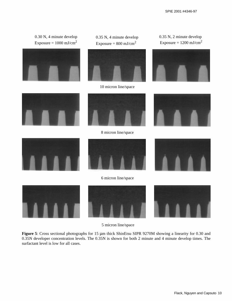
Cross sectional photographs were used to determine the impact of the developer conditions on resolution andphotoresist profiles (Figure 5). It is clear looking at the 0.35N for 4 and 2 minute develop times that the top lossof the smaller features is extremely large. The 0.30N developer shows excellent resolution and full photoresist
retention even at 5 µm features. Based on these results it was determined that the 0.35 normal developer was notviable. The top loss and lack of process window made the very highest normality unacceptable.
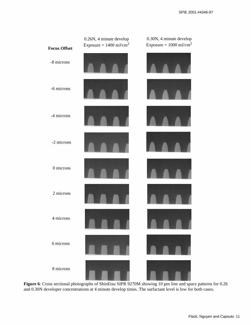
Figure 6 shows cross sectional photographs of 10 µm features through focus for the 0.26N and 0.30N developerswith a 4 minute develop time. At minus focus offsets the 0.30N developer shows more profile rounding than the0.26N. This would reduce the effective DOF for the case were electroplating to the top of the photoresist thick-ness is required. However, the side wall angle at the base of the photoresist is comparable for both developer nor-malities through the focus range. Either developer would be acceptable for the case of electroplating up to 70percent of the photoresist thickness.
A linearity analysis was used to more closely examine the 0.26 and the 0.30N developers (Figure 4). This plotwas constructed using top down SEM data for isolated spaces and is a best fit plot of the data. The 0.26N devel-oper shows excellent linearity across the range of sizes. The 0.30N developer shows some deviation from linear-ity for the small feature sizes. However, there is not a significant difference between the two develop times at0.30N. It appears that with the 0.30N developer it is possible to reduce the develop time by 1 minute compared tothe 0.26N developer. The shorter develop time with the 0.30N developer could be used to increasing lithographycell productivity and reduce total cost of ownership.

Flack, Nguyen and Capsuto 5
SPIE 2001 #4346-97
3.2 Surfactant Level Comparison
Figure 7 shows cross sectional SEMs of 10 µm features through DOF comparing low and high surfactant for the0.30N developer using a 4 minute develop time. Low surfactant is defined as surface tension of 43 dyne/cm whilehigh surfactant level is defined as surface tension of 40 dyne/cm. There is very little profile change between thetwo different surfactant levels. As a result it is necessary to perform a more comprehensive process capabilityanalysis to determine the effect of the surfactant level.
Figure 8 shows process window plots for 10 µm features for low and high surfactant for the 0.26N at 4 minutes (aand b), the 0.30N developer for 3 minutes (c and d) and the 0.30N developer for 4 minutes (e and f). The shadedenvelope on each plot defines the area with ten percent CD control limit for a 10 µm spacewidth. The largestrectangular process window that fits within the envelope is also shown. There is a significant difference betweenthe process windows for the different surfactant levels. The lower surfactant level in all cases gave a largerprocess window in terms of exposure latitude with no difference in focus latitude. However, the higher surfactantlevel cut the optimum exposure by an average of 11 percent. Each graph shows the optimum focus position(marked F) and optimum exposure condition (marked E). Clearly the choice of surfactant level depends on thetrade off between process requirements and increased throughput.
3.3 Wavelength Comparison
Cross sectional SEMs were used to determine the impact of the exposure wavelength on resolution andphotoresist profiles. Figure 9 shows ghi-line and gh-line exposure for a CD range of 2 to 10 µm. The gh-lineshows better resolution, sidewall angles and film retention than the ghi-line exposure. Traditionally very thicknovolak photoresist performs better with just gh-line. At i-line the bulk absorption of the photoresist is so largethat it requires higher exposures in order to clear out the base of the photoresist. This extremely high exposurecauses top loss and general profile degradation. Also the exposure bias has a tendency to be higher. When the i-line component is removed the transparency improves throughout the entire thickness of the photoresist. Figure 9clearly shows this phenomena especially for smaller feature sizes.
4.0 CONCLUSIONS
This paper has explored the performance of an ultra-thick photoresist for high aspect ratio micromachining andflipchip bump bond applications on the Ultratech Spectrum 3 stepper utilizing ShinEtsu SIPR 9270M photoresistand Moses Lake developers. Standard photoresist characterization techniques have been applied to evaluate theeffects of developer concentration, surfactant levels and exposure wavelength. Features as small as 2 µm wereobserved in 15 µm thick films.
The use of 0.35N developer is not acceptable in terms of photoresist performance while the 0.30N and 0.26Ngave acceptable performance. The 0.30N developer allowed the develop time to be reduced by 25% over the0.26N, increasing the lithography cell throughput and reducing cost of ownership. The lower surfactant level inall cases gave a larger process window, however the higher surfactant level cut the optimum exposure by anaverage of 11%. The use of gh-line exposure for ultra-thick photoresist showed improved resolution and sidewallcontrol as compared to ghi-line.
Over all, thick photoresist film processes can be improved dramatically with the use of higher level normality, achange in surfactant levels and a choice of wavelength. Follow up work can be done to further optimize theprocess by changing the softbake temperature/time, developer temperature, wait times and develop method

Flack, Nguyen and Capsuto 6
SPIE 2001 #4346-97
(immersion verses puddle). Clearly the decision to implement a higher level surfactant depends on the trade offbetween process requirements and increased throughput requirements.
A summary of recommended developer conditions is given in Table 3.
5.0 ACKNOWLEDGEMENTS
The authors would like to thank Ted Endo from Moses Lake Industries for providing developer, Mr. H. Kato fromShinEtsu Chemical and Mr. K. Toba from ShinEtsu Chemical for photoresist support and Hai Nguyen ofUltratech Stepper for support with CD measurements and cross sectional analysis.
6.0 REFERENCES
1. J. Knutti, “Finding Markets For Microstructures”, Micromachining and Fabrication process Technology IV Proceedings, SPIE 3511, 1998, pg.17-23.
2. R. Wechsung, N. Unal, “Market Analysis for Microsystems: an Interim Report From the Nexus Task Force”, Micro System Technologies 98 Proceedings, December 3, 1998, pg. 275.
3. Lau, “Next Generation Low Cost Flip Chip Technologies,” 46th Electronic Components & Technology Conference, 1996.
4. M. Madou, “Fundamentals of Microfabrication”, CRC Press, 1997, pg. 325-368.
5. Gau, J.S., “Photolithography for Integrated Thin-Film Read/Write Heads”, Optical/Laser Microlithography II”, SPIE 1088, 1989, pg 504-514.
6. S. Mansfield et. al., “Lithographic Comparison of Assist Feature Design Strategies”, Optical Microlithography XIII, SPIE 4000 (2000), pp. 63-76.
7. W. Flack, W. Fan, S. White, “The Optimization and Characterization of Ultra-thick Photoresist Films,” Advances in Resist Technology and Processing XV Proceedings, SPIE 3333, 1998, pg. 1288-1303.
8. W. Flack, W. Fan, S. White, “Characterization of Ultra-thick Photoresists for MEMS Applications Using a 1X Stepper”, Materials and Device Characterization in Micromachining Proceedings, SPIE 3512, 1998, pg. 296-315.
9. W. Flack, S. White, B. Todd, “Process Characterization of One Hundred Micron Thick Photoresist Films”, Advances in Resist Technology and Processing XVI Proceedings, SPIE 3678, 1999, pg. 474-490.
10. L. Tong et al., “Application of Resolution Enhancement Techniques in Thin Film Head Processing”, Metrology, Inspection, and Process Control for Microlithography XIII Proceedings, SPIE 3677 1999, pg. 3677-88.
11. Flores, Flack, Dwyer, “Lithographic Performance of a New Generation i-line Optical System,” Optical/Laser Lithography VI Proceedings, SPIE 1927, 1993.

Flack, Nguyen and Capsuto 7
SPIE 2001 #4346-97
Table 1: Optical specifications of the Spectrum 3 stepper used in this study.
Table 2: Process conditions for ShinEtsu SIPR 9270M for 15 µm thickness.
Table 3: Recommended developer conditions for 15 µm Shin-Etsu SIPR 9270M on a Spectrum 3 stepper.
Parameter Spectrum 3Reduction factor 1X
Wavelength (nm) 350 - 450
Numerical aperture (NA) 0.16
Partial coherence (σ) 1.0
Wafer plane irradiance (mW/cm2) 1750
Process Step Parameters EquipmentVapor Prime HMDS 20 minutes YES Oven
SIPR 9270M Coat Static dispense; Spin: 2750 rpm for 20 seconds MTI Coater
Softbake 180 seconds at 110oC, contact
1 hour wait time before exposure
MTI Hotplate
Develop 1 hour wait time after exposure
Moses Lake Experimental developer at 21oC
2 to 4 minutes immersion with agitation
Batch
Rinse Dump Rinse with DI water; Spin rinse and dry Batch
Developer Type 0.26N, Low Surfactant 0.30N, Low SurfactantDevelop Time (minutes) 4 3
Nominal Exposure (mJ/cm2) 1210 1060
Exposure Latitude (mJ/cm2) 400 300
Focus Latitude (µm) 16 16

Flack, Nguyen and Capsuto 8
SPIE 2001 #4346-97
Figure 1: Wafer layout for the focus and exposure matrix. A nine by nine field array was exposed with focusvarying in the horizontal axis and exposure dose varying in the vertical axis.
Figure 2: Contrast curves for 0.26, 0.30 and 0.35N developer concentrations. The surfactant level is low for allcases.
Exposure
Focus
Individual Field
line/spaces
X
2

Flack, Nguyen and Capsuto 9
SPIE 2001 #4346-97
Figure 3: Exposure latitude for 10 µm spacewidths at 0.26, 0.30 and 0.35N developer concentrations. Thesurfactant level is low for all cases.
Figure 4: Mask linearity plot for 15 µm thick ShinEtsu SIPR 9270M. The exposure dose for the 0.26N developerwas 1500 mJ/cm2. The exposure dose for the 0.30N developer was 1200 mJ/cm2 for 3 minutes and 1100 mJ/cm2
for 4 minutes. The surfactant level is low for all cases.
2
0.26N, 4min
0.30N, 3 min
0.30N, 4min
Flack, Nguyen and Capsuto 10
SPIE 2001 #4346-97
Figure 5: Cross sectional photographs for 15 µm thick ShinEtsu SIPR 9270M showing a linearity for 0.30 and0.35N developer concentration levels. The 0.35N is shown for both 2 minute and 4 minute develop times. Thesurfactant level is low for all cases.
10 micron line/space
0.30 N, 4 minute develop 0.35 N, 2 minute develop
8 micron line/space
6 micron line/space
5 micron line/space
0.35 N, 4 minute developExposure = 1000 mJ/cm2 Exposure = 1200 mJ/cm2
Exposure = 800 mJ/cm2
Flack, Nguyen and Capsuto 11
SPIE 2001 #4346-97
Figure 6: Cross sectional photographs of ShinEtsu SIPR 9270M showing 10 µm line and space patterns for 0.26and 0.30N developer concentrations at 4 minute develop times. The surfactant level is low for both cases.
0.30N, 4 minute developExposure = 1000 mJ/cm2
-8 microns
-6 microns
-4 microns
-2 microns
0 microns
2 microns
4 microns
6 microns
8 microns
Focus Offset
0.26N, 4 minute developExposure = 1400 mJ/cm2

Flack, Nguyen and Capsuto 12
SPIE 2001 #4346-97
Figure 7: Cross sectional photographs of ShinEtsu SIPR 9270M showing 10 µm line and space patterns for0.30N developer with low and high surfactant levels. The exposure dose is 1000 mJ/cm2 for both cases.
0.30N, 4 minute developLow surfactant
-8 microns
-6 microns
-4 microns
-2 microns
0 microns
2 microns
4 microns
6 microns
8 microns
Focus Offset
0.30N, 4 minute develop
High surfactant

Flack, Nguyen and Capsuto 13
SPIE 2001 #4346-97
Figure 8: Process window for 10 µm spacewidth in 15 µm thick ShinEtsu SIPR 9270M exposed with ghi-line.The process envelope shows ±10 percent control limits.
800
1000
1200
1400
1600
-8 -7 -6 -5 -4 -3 -2 -1 0 1 2 3 4 5 6 7 8
Exp
osu
re D
ose
(mJ/
cm2)
Focus (microns)
F 0.00E 1212
800
1000
1200
1400
1600
-8 -7 -6 -5 -4 -3 -2 -1 0 1 2 3 4 5 6 7 8
Exp
osu
re D
ose
(mJ/
cm2)
Focus (microns)
F 0.0E 1136
800
1000
1200
1400
1600
-8 -7 -6 -5 -4 -3 -2 -1 0 1 2 3 4 5 6 7 8
Exp
osu
re D
ose
(mJ/
cm2)
Focus (microns)
F 0.00E 1059
800
1000
1200
1400
1600
-8 -7 -6 -5 -4 -3 -2 -1 0 1 2 3 4 5 6 7 8
Exp
osu
re D
ose
(mJ/
cm2)
Focus (microns)
F 0.00E 939
800
1000
1200
1400
1600
-8 -7 -6 -5 -4 -3 -2 -1 0 1 2 3 4 5 6 7 8
Exp
osu
re D
ose
(mJ/
cm2)
Focus (microns)
F 0.00E 980
800
1000
1200
1400
1600
-8 -7 -6 -5 -4 -3 -2 -1 0 1 2 3 4 5 6 7 8
Exp
osu
re D
ose
(mJ/
cm2)
Focus (microns)
F 0.0E 810
(a) 0.26N, Low surfactant, 4 minute develop (b) 0.26N, High surfactant, 4 minute develop
(c) 0.30N, Low surfactant, 3 minute develop (d) 0.30N, High surfactant, 3 minute develop
(e) 0.30N, Low surfactant, 4 minute develop (f) 0.30N, High surfactant, 4 minute develop

Flack, Nguyen and Capsuto 14
SPIE 2001 #4346-97
Figure 9: Cross sectional photographs of ShinEtsu SIPR 9270M showing linearity at 1100 mJ/cm2 for ghi-lineand gh-line exposure wavelengths. The focus offset is zero for all cases. The developer time was 3 minutes at0.30N concentration with low surfactant level.
10 micron line/space
ghi-line Exposure
8 micron line/space
6 micron line/space
4 micron line/space
gh-line Exposure
3 micron line/space
2 micron line/space
Linesize