pro f. a. r. newto n final examination group 1
TRANSCRIPT
Your Name: _______________________________________
Final Group 1 Page 1 of 12 CS 150 - Sp. 94
UN IVERSIT Y O F CA LIFO RNI A AT BERKELEY
BER KELEY • D AV IS • IR VINE • LOS A N GELES • RIVERS IDE • SAN D IEGO • S AN FRANCISCO SA N TA BA RBA RA • S AN TA CRUZ
De p a r tm en t of Ele ct r i ca l En gin e e rin g a n d Com p u t e r Scien c es
CS 1 5 0 - Spr i n g 1 99 4 Pr o f. A. R. Ne wt o n
Final Examination Group 1Room 1 Physical Science, 8am Friday 5/13(Open Katz only, Calculators OK, 3 hours)
Include all final answers in locations indicated on these pages. Use space provided for all working. If necessary,attach additional sheets by staple at the end. BE SURE TO WRITE YOUR NAME ON EVERY SHEET.
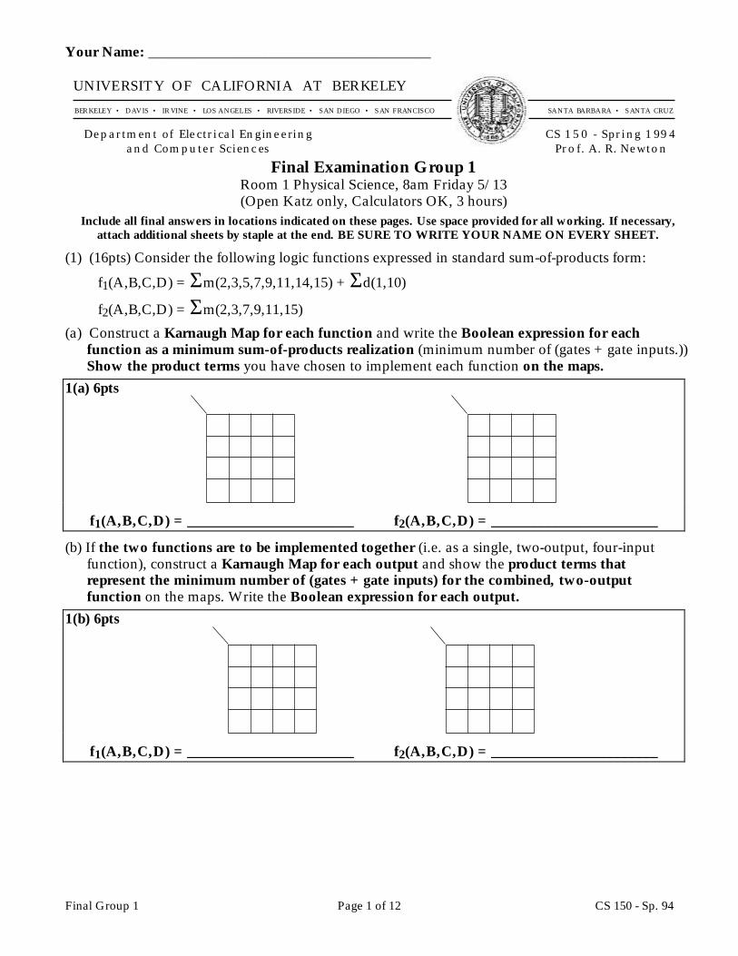
(1) (16pts) Consider the following logic functions expressed in standard sum-of-products form:
f1(A,B,C,D) = Σm(2,3,5,7,9,11,14,15) + Σd(1,10)
f2(A,B,C,D) = Σm(2,3,7,9,11,15)(a) Construct a Karnaugh Map for each function and write the Boolean expression for each
function as a minimum sum-of-products realization (minimum number of (gates + gate inputs.))Show the product terms you have chosen to implement each function on the maps.
1(a) 6pts
f1(A,B,C,D) = _______________________ f2(A,B,C,D) = _______________________
(b) If the two functions are to be implemented together (i.e. as a single, two-output, four-inputfunction), construct a Karnaugh Map for each output and show the product terms thatrepresent the minimum number of (gates + gate inputs) for the combined, two-outputfunction on the maps. Write the Boolean expression for each output.
1(b) 6pts
f1(A,B,C,D) = _______________________ f2(A,B,C,D) = _______________________

CS 150 - Sp. 94 Page 2 of 12 Final Group 1
(c) Considering the first function f1(A,B,C, D) = Σm(2,3,5,7,9,11,14,15) + Σd(1,10) only,draw a schematic diagram for f1 that uses the minimum number of logic gates. Use onlyAND, OR, and inverter gates and assume input complements are not available (i.e. aninverter counts as a gate.)
1(c) 4pts
Additional space for Problem 1

Your Name: _______________________________________
Final Group 1 Page 3 of 12 CS 150 - Sp. 94
(2) (16pts) Consider the logic function shown below in Karnaugh Map form. In all parts to thisquestion, assume input complements are not available (i.e. an inverter counts as a gate.)
f(A,B,C,D) =
AB00 01 11 10
00
01
11
10
CD
1
1
1
1
1
1
1
1
0
0
0
0
0
0
0
0
(a) Derive an implementation of this function using a single 8-input, 3-control-line multiplexerand a minimum number of logic gates.
2(a) (4pts)
(b) Derive an implementation of the function using a single 4-input, 2-control-line multiplexer anda minimum number of two-input XOR gates and inverters only.
2(b) (4pts)

CS 150 - Sp. 94 Page 4 of 12 Final Group 1

Your Name: _______________________________________
Final Group 1 Page 5 of 12 CS 150 - Sp. 94
(c) Implement the function using a minimum number of simple logic gates (AND, OR, NAND,NOR, XOR, XNOR, and inverters only.)
2(c) (4pts)
(d) Construct the PLA-format table representation for the function in AND-OR form. How manyproduct terms would an AND-OR PLA implementation require?
2(d) (2pts)
Product terms: __________
(e) If the function were implemented using a ROM, how many ROM storage locations would berequired? How many address inputs would the ROM have?
2(e) (2pts)Storage Locations: _________ Address inputs: _________
Additional space for Problem 2
CS 150 - Sp. 94 Page 6 of 12 Final Group 1
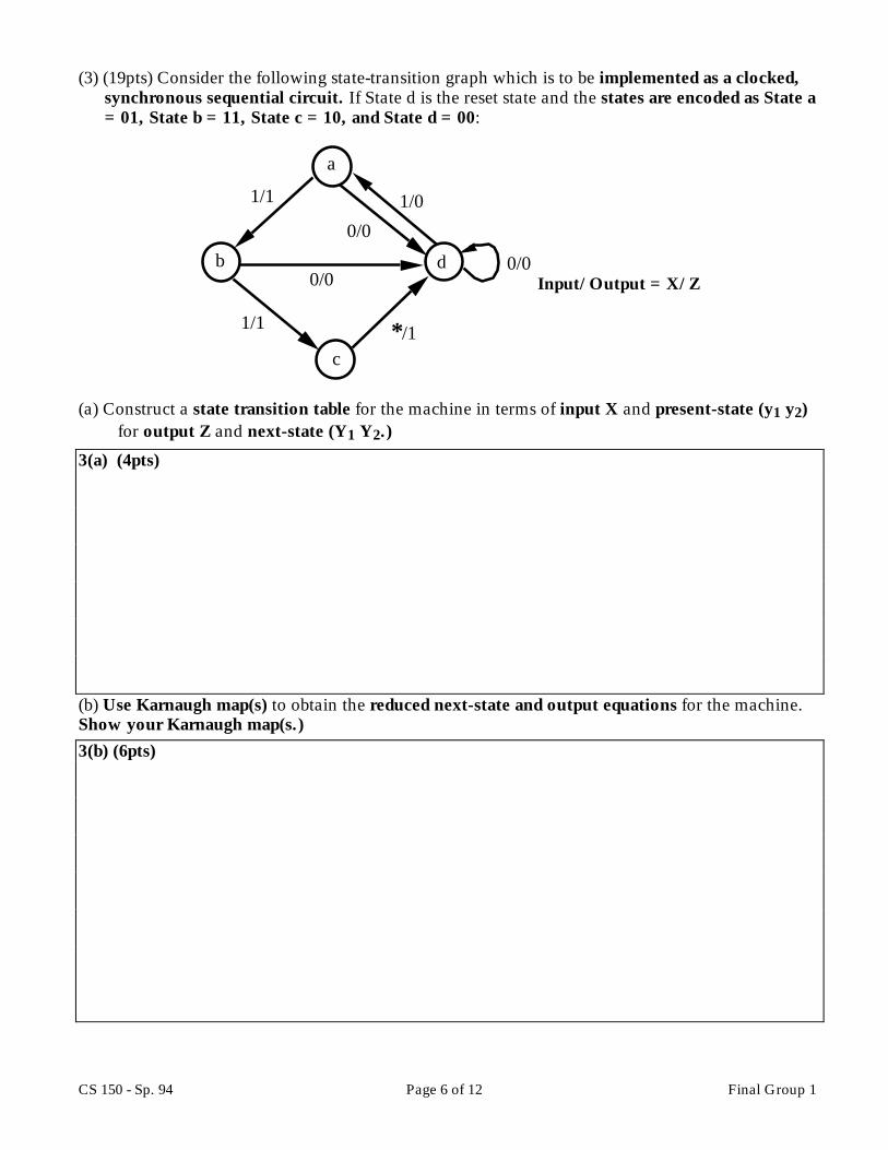
(3) (19pts) Consider the following state-transition graph which is to be implemented as a clocked,synchronous sequential circuit. If State d is the reset state and the states are encoded as State a= 01, State b = 11, State c = 10, and State d = 00:
0/0
1/0
1/1 */1
0/0
1/1
a
b
c
d0/0 Input/Output = X/Z
(a) Construct a state transition table for the machine in terms of input X and present-state (y1 y2)for output Z and next-state (Y1 Y2.)
3(a) (4pts)
(b) Use Karnaugh map(s) to obtain the reduced next-state and output equations for the machine.Show your Karnaugh map(s.)3(b) (6pts)

Your Name: _______________________________________
Final Group 1 Page 7 of 12 CS 150 - Sp. 94
(c) Use the reduced set of equations to obtain a circuit diagram for an implementation of themachine. Use the minimum number of logic gates (AND, OR, NAND, NOR, XOR, XNOR, orinverters) and positive-edge-triggered toggle (T) flip-flops only.
3(c) (6pts)
(c) Using your next-state table from Part 3(a) above, construct an implication table and check forstate equivalence. List the equivalent states. Enter the word NONE below if you cannot find anyequivalent states from your table.
3(d) (4pts)
Equivalent States: ______________
Additional space for Problem 3

CS 150 - Sp. 94 Page 8 of 12 Final Group 1
(4) (14pts) A clocked, synchronous sequential circuit is to be designed as follows:
“The circuit is to have a single input, X, that is used to control two outputs Z1 and Z2.While X is 1, (Z1,Z2) = (00) . When X becomes 0, the outputs (Z1,Z2) begin thesequence (00, 01, 11, 10) . If they reach the value 10 they hold that value until theinput changes to 1 again.”
(a) Construct a state transition graph (STG) for the machine in Mealy form.3(a) (4pts)
(b) Convert your STG to Moore form and make a state assignment that minimizes the amount ofoutput logic needed for a Moore implementation of the machine.3(b) (4pts)

Your Name: _______________________________________
Final Group 1 Page 9 of 12 CS 150 - Sp. 94
(c) Determine the next-state and output equations for your machine and implement the circuitusing positive edge-triggered D flip-flops and a minimum number of two-input NAND gatesonly. Assume X comes from the output of another flip-flop and so the complement of X is alsoavailable.
3(b) (6pts)
Additional space for Problem 4

CS 150 - Sp. 94 Page 10 of 12 Final Group 1
(5) (18pts) (a) What is a fundamental-mode asynchronous circuit? Give a concise definition.5(a) (4pts)
Consider the state diagram for the asynchronous sequential machine shown below.
0/0
1/0
1/0 1/0
1/1 a
b
c
d
0/0
0/0
0/0
(b) Draw a primitive flow table for the machine, indicating all stable states and outputs.5(b) (4pts)
(c) With the code for State a given as all 0’s derive a race-free state assignment for the machineusing a minimum number of internal state variables. Show all working.5(c) (4pts)
a = ______ b = _____ c = _____ d = ______

Your Name: _______________________________________
Final Group 1 Page 11 of 12 CS 150 - Sp. 94
(d) Provide a schematic diagram for the machine using a minimum number of logic gates (AND,OR, NAND, NOR, XOR, XNOR, or inverters). Indicate your state variables as labels on buffersymbols. Ensure that the output logic cannot produce glitches and state why that is so.
3(b) (6pts)
Additional space for Problem 5

CS 150 - Sp. 94 Page 12 of 12 Final Group 1
(6) (17pts)(a) Draw the block diagram for a sequential, 32-bit full-adder that uses a single, one-bit full adderand two 32-bit serial shift registers to perform addition of two unsigned, 32-bit binary numbers.Explain how the adder operates and how overflow would be detected if it occurred.
6(a) (6pts)
(b) With the addition of a single “add/subtract “ input and logic gates, modify your design toperform addition or subtraction of two unsigned binary numbers.
6(b) (4pts)

Your Name: _______________________________________
Final Group 1 Page 13 of 12 CS 150 - Sp. 94
(c) Derive a block diagram for a bit-serial sequential circuit that can be used for comparing therelative magnitudes of two 32-bit numbers, A<31:0> and B<31:0>, stored in sign-magnitudeform, where bit 31 is the sign bit. Do not use subtraction. Describe how your circuit operates.
6(c) (7pts)
Additional space for Problem 6