printing conductive nanomaterials for flexible and
TRANSCRIPT

Review
1800546 (1 of 41) © 2019 WILEY-VCH Verlag GmbH & Co. KGaA, Weinheim
www.advmattechnol.de
Printing Conductive Nanomaterials for Flexible and Stretchable Electronics: A Review of Materials, Processes, and Applications
Qijin Huang and Yong Zhu*
DOI: 10.1002/admt.201800546
manufacturing processes and relatively high production cost.[12,13] PE has been explored for the manufacturing of flex-ible and stretchable electronic devices by printing functional inks containing sol-uble or dispersed materials,[14–16] which has enabled a wide variety of applications, such as transparent conductive films (TCFs), flexible energy harvesting and storage, thin film transistors (TFTs), elec-troluminescent devices, and wearable sen-sors.[17–24] The global PE market should reach $26.6 billion by 2022 from $14.0 bil-lion in 2017 at a compound annual growth rate of 13.6%.[25]
PE devices are manufactured by a variety of printing technologies. Typical printing technologies can be divided into two broad categories: noncontact pat-terning (or nozzle-based patterning) and contact-based patterning. The noncontact techniques include inkjet printing, electro-hydrodynamic (EHD) printing, aerosol jet printing, and slot die coating, while screen printing, gravure printing, and flexog-raphic printing are examples of the contact
techniques. Each of these techniques has its own advantages and disadvantages, but they all rely on the principle of trans-ferring inks to a substrate. Understanding the characteristics and recent advances of each printing technique is important to further the progress in PE. Moreover, to promote the lab-scale printing technologies to large-scale production process, roll-to-roll (R2R) printing, which is one of the manufacturing methods to obtain large-area films with low cost and excellent durability, has drawn much attention from both industry and the research community.
Nearly all of devices based on PE require conductive struc-tures, interconnects, and contacts; therefore, highly conductive patterns, usually with high transparency and/or high resolu-tion, fabricated by means of printing conductive materials are one of the most critical components in PE devices. Various printable conductive nanomaterials, such as metal nanoma-terials (e.g., metal nanoparticles and metal nanowires) and carbon nanomaterials (e.g., graphene and carbon nanotubes (CNTs)), have been explored and used as major materials for PE. Applying printing technology to deposition of the conduc-tive nanomaterials requires formulation of suitable inks. After depositing inks on different substrates, post-printing treatment,
Printed electronics is attracting a great deal of attention in both research and commercialization as it enables fabrication of large-scale, low-cost electronic devices on a variety of substrates. Printed electronics plays a critical role in facilitating widespread flexible electronics and more recently stretchable elec-tronics. Conductive nanomaterials, such as metal nanoparticles and nano-wires, carbon nanotubes, and graphene, are promising building blocks for printed electronics. Nanomaterial-based printing technologies, formulation of printable inks, post-printing treatment, and integration of functional devices have progressed substantially in the recent years. This review summarizes basic principles and recent development of common printing technologies, formulations of printable inks based on conductive nanomaterials, deposi-tion of conductive inks via different printing techniques, and performance enhancement by using various sintering methods. While this review places emphasis on conductive nanomaterials, the printing techniques and ink formulations can be applied to other materials such as semiconducting and insulating nanomaterials. Moreover, some applications of printed flexible and stretchable electronic devices are reviewed to illustrate their potential. Finally, the future challenges and prospects for printing conductive nanomaterials are discussed.
Dr. Q. Huang, Prof. Y. ZhuDepartment of Mechanical and Aerospace EngineeringNorth Carolina State UniversityRaleigh, NC 27695-7910, USAE-mail: [email protected]
The ORCID identification number(s) for the author(s) of this article can be found under https://doi.org/10.1002/admt.201800546.
Printed Electronics
1. Introduction
Printed electronics (PE) refers to a type of electronics that are created by conventional printing technologies and has received tremendous attention in recent years.[1–5] The key advantages of PE include low-cost manufacturing with high throughput, compatibility with flexible systems (e.g., large-area electronics and hybrid system fabrication on flexible or stretchable sub-strates utilizing inorganic, organic, and bioinspired materials), and relative ease of integration.[6–11] By contrast, silicon-based microfabrication technologies, such as photolithography and vacuum-based techniques (e.g., evaporation, sputtering, and chemical vapor deposition), typically require complicated
Adv. Mater. Technol. 2019, 4, 1800546

www.advancedsciencenews.com
© 2019 WILEY-VCH Verlag GmbH & Co. KGaA, Weinheim1800546 (2 of 41)
www.advmattechnol.de
usually thermal sintering, is required to obtain highly con-ductive patterns. To be compatible with common flexible and elastic substrates, alternative sintering methods are required to reduce the manufacturing costs and shorten the processing time. As such, the scope of this review is focused on the use of silver nanoparticles (AgNPs), silver nanowires (AgNWs), copper nanoparticles (CuNPs), copper nanowires (CuNWs), graphene, and CNTs including single-walled CNTs (SWNTs) and multiwalled CNTs (MWNTs) as the materials of choice for PE, with emphasis on their fabrication using different printing technologies and sintering techniques. As to be reviewed, the conductive nanomaterials can be widely used in the broad field of printable flexible and stretchable electronics. A brief histor-ical road map, which focuses on printing conductive nanomate-rials, is shown in Figure 1.[6,11,14,19,26–44]
For the rest of this review, in Section 2, we describe the fundamental principles and recent advances of different types of printing techniques, including inkjet printing, electrohy-drodynamic printing, aerosol jet printing, slot die coating, screen printing, gravure printing, flexographic printing, and R2R printing. Then, in Section 3, we introduce synthesis of metal-based nanomaterials and carbon nanomaterials and formulation of corresponding inks for various printing pro-cesses. In Section 4, we present development of depositing the inks using the aforementioned printing techniques. In Section 5, a number of post-printing treatment methods to convert the printed ink into conductive patterns are dis-cussed. In Section 6, we discuss applications of conductive nanomaterials to fabricate functional devices. Research chal-lenges, opportunities, and future developments in the field of printable flexible and stretchable electronics are discussed in the final section.
2. Printing Technology: Materials and Recent Development
Conductor, semiconductor, and dielectric have all been fab-ricated by printing. Conductor is an essential component for flexible and stretchable electronic devices; the earliest printed materials are mostly conductors. From the printing perspec-tive, nanomaterials show particular promise as they can be dispersed in various solvents to form inks compatible with printing technologies while maintaining unique and desirable materials properties. Thus, conductive nanomaterials have been widely used for the development of flexible and stretchable electronics. In view of the vast existing literature on printing technologies,[45–47] this section will only give a brief introduc-tion to the fundamentals of common printing technologies and focus on their recent development.
2.1. Printable Conductive Nanomaterials
Among the conductive nanomaterials, metals represent the main system of choice. Ag has the highest room-temperature electrical conductivity, by virtue of which Ag nanomaterials, such as AgNPs and AgNWs, are the most extensively studied metal nanostructures as conductors or electrodes for PE.[48–54]
Qijin Huang received his B.S. degree in Materials Chemistry from Qingdao University of Science and Technology in 2009, and M.S. degree in Materials Engineering and Ph.D. degree in Materials Physics and Chemistry from University of Chinese Academy of Sciences in 2012 and 2015, respectively. He then did his postdoctoral
research in North Carolina State University. His research interests focus on printing conductive nanomaterials for flexible and stretchable electronics.
Yong Zhu is a Professor in Departments of Mechanical and Aerospace Engineering, Biomedical Engineering, and Materials Science and Engineering at North Carolina State University. He received his B.S. degree in Mechanics and Mechanical Engineering from the University of Science and Technology of China in 1999, and his M.S. and Ph.D.
degrees in Mechanical Engineering from Northwestern University in 2001 and 2005, respectively. His research interests include mechanics of nanomaterials, micro/nano-electromechanical systems, and flexible/stretchable electronics.
Since Cu possesses a very high conductivity (only 6% less than that of Ag) and is much cheaper, CuNPs and CuNWs for PE have also drawn much attention.[55–57] Moreover, metal grids based on metal NPs and metal NW networks with large length-to-diameter aspect ratio of metal NWs show high transmit-tance, good conductivity, and excellent mechanical compliancy.
In addition to metal nanomaterials, carbon nanomaterials, including graphene and CNTs, are also promising in printable flexible and stretchable electronics due to their unique proper-ties, such as high intrinsic current mobility and mechanical flexibility.[3,36,58–64]
2.2. Inkjet Printing
2.2.1. Conventional Inkjet Printing Process
Inkjet printing is a material-conserving deposition technique for printing functional patterns.[65–68] Nanomaterials in the form of colloidal dispersion are deposited through the microm-eter-sized printing nozzle. The advantages of inkjet printing
Adv. Mater. Technol. 2019, 4, 1800546

www.advancedsciencenews.com
© 2019 WILEY-VCH Verlag GmbH & Co. KGaA, Weinheim1800546 (3 of 41)
www.advmattechnol.de
Adv. Mater. Technol. 2019, 4, 1800546
Figure 1. A brief historical road map of printed electronics: “Screen printing silver contact for silicon solar cells,” Reproduced with permission.[26] Copyright 1984, IEEE. “Inkjet printing silver grid on solar cells.” Reproduced with permission.[27] Copyright 1988, IEEE. “Screen printing field-effect tran-sistor.” Reproduced with permission.[28] Copyright 1997, American Chemical Society. “Inkjet printing polymer light-emitting devices.” Reproduced with permission.[29] Copyright 1998, AIP Publishing. “Printing all-inorganic transistor.” Reproduced with permission.[30] Copyright 1999, American Associa-tion for the Advancement of Science. “Inkjet printing transistor circuits.” Reproduced with permission.[31] Copyright 2000, American Association for the Advancement of Science. “Electrohydrodynamic printing functional devices.” Reproduced with permission.[32] Copyright 2007, Springer Nature. “Aerosol jet printing transistor array.” Reproduced with permission.[33] Copyright 2011, Springer Nature. “Dispense printing Ag wires.” Reproduced with permis-sion.[6] Copyright 2009, American Association for the Advancement of Science. “Printed transistors.” Reproduced with permission.[34] Copyright 2009, Springer Nature. “Double-shot inkjet printing single crystal film.” Reproduced with permission.[14] Copyright 2011, Springer Nature. “Screen printing graphene electrode.” Reproduced with permission.[35] Copyright 2011, IEEE. “Inkjet printing graphene electronics.” Reproduced with permission.[36] Copyright 2012, American Chemical Society. “Gravure printing graphene electrode.” Reproduced with permission.[37] Copyright 2014, Wiley-VCH. “Inkjet printing liquid metal.” Reproduced with permission.[38] Copyright 2015, Wiley-VCH. “Fully slot-die coating perovskite solar cells.” Reproduced with per-mission.[40] Copyright 2015, Wiley-VCH. “Inkjet printing silver nanowires.” Reproduced with permission.[39] Copyright 2015, American Chemical Society. “Screen printing silver nanowires.” Reproduced with permission.[19] Copyright 2016, Wiley-VCH. “All inkjet-printed 2D material transistors.” Reproduced with permission.[41] Copyright 2017, American Association for the Advancement of Science. “Printable elastic conductor for wearable devices.” Repro-duced with permission.[11] Copyright 2017, Springer Nature. “All inkjet-printed 2D material photodetectors and read-only memory.” Reproduced with permission.[42] Copyright 2017, Springer Nature. “Stretchable, inkjet-printed thin-film electronics.” Reproduced with permission.[44] Copyright 2018, Wiley-VCH. “Electrohydrodynamic printing silver nanowire stretchable conductor.” Reproduced with permission.[43] Copyright 2018, Royal Society of Chemistry.

www.advancedsciencenews.com
© 2019 WILEY-VCH Verlag GmbH & Co. KGaA, Weinheim1800546 (4 of 41)
www.advmattechnol.de
Adv. Mater. Technol. 2019, 4, 1800546
Figure 2. a) Schematic of CIJ printing. Schematics of DOD inkjet printing, where the pressure can be provided by b) vapor bubble generated by a thin film heater (thermal inkjet) or c) a piezoelectric actuator (piezoelectric inkjet). d) Schematic of double-shot inkjet printing. e) Images of inkjet-printed

www.advancedsciencenews.com
© 2019 WILEY-VCH Verlag GmbH & Co. KGaA, Weinheim1800546 (5 of 41)
www.advmattechnol.de
include accurate and rapid deposition of a broad range of functional materials in a large area at low cost, a possibility of depositing very small amount of the material (e.g., depositing picoliter droplets), and easy integration of different materials on the same substrate.[67,69] Moreover, as a noncontact and maskless deposition technique, the contamination of the sub-strate is minimized.[51,70]
There are two major mechanisms by which inkjet printers generate droplets—continuous inkjet (CIJ) printing and drop-on-demand (DOD) inkjet printing.[66,71,72] In the CIJ mode (Figure 2a), pressurized ink is forced through a nozzle, and breaks up into uniform drops under the action of surface ten-sion. The DOD mode, in turn, is characterized by smaller drop size and higher placement accuracy. In this mode, drops are ejected by a pressure pulse generated in a fluid-filled cavity behind the printing nozzle. The pressure pulse that drives drop formation can be generated either by a thermal pulse cre-ating a vapor bubble (Figure 2b) or by a piezoelectric actuator (Figure 2c). CIJ mode inkjet printers are now robust industrial tools and are widely used for high-speed graphical applications. However, they have been little used in materials science applica-tions, due to potential contamination of the ink after recycling and more limited range of fluids that can be deposited.[71] This review thus focuses on applications of DOD inkjet printing in materials science.
In the printing process, to avoid the aggregation of compo-nents that would clog the print head nozzle, inks used for the fabrication of inkjet-printed functional materials should have properties that are equivalent to those of standard inkjet printer inks.[72] Particle size, viscosity, surface tension, and density of the ink play key roles in the formation and behavior of liquid jet and drops generated in a DOD printer. They can be char-acterized by a number of dimensionless groupings of physical constants, the most useful of which are the Reynolds (Re), Weber (We), and Ohnesorge (Oh) numbers
νρη
=Rea
(1)
ν ργ
=2
Wea
(2)
OhWe
Re a
ηγρ
= = (3)
where ρ, η, and γ are the density, viscosity, and surface ten-sion of the ink, respectively, ν is the velocity, and a is charac-teristic length, typically the diameter of the nozzle. Generally, a Z value is suggested using Z = 1/Oh as the figure of merit to characterize drop formation, where a value between 1 and 14 means the stable drop formation.[36,75] At a small Z value, viscous dissipation in the ink prevents drop formation, while at a large value, the primary drop is accompanied by a large
number of satellite drops.[76] It should be noted that the longest dimension of the nanomaterials should be less than a/50 to eliminate nozzle clogging during printing.[39,77] Thus, for 1D nanomaterials (e.g., AgNWs), length trimming is often needed before printing. However, this requirement might not be as stringent for 1D nanomaterials due to the possibility of shear flow–induced alignment as the 1D nanomaterials pass through the nozzle.[39]
Coffee ring effect, which originates from the capillary flow induced by the differential evaporation rates across the drop, is a common phenomenon in printing process.[78] When one droplet has a pinned three-phase contact line, the excess solvent lost at the edge is replenished by solvent in the center, leading to a radial capillary flow. The capillary flow carries the solutes in evaporating droplet toward the pinned three-phase contact line, carrying nearly all the dispersed material to the edge; thus, the ring-like morphology is formed.[79] Coffee ring effect directly influences the morphologies of patterns deposited on the sub-strate, which affects the resolution of patterns and the perfor-mance of devices.[79,80] Such an effect is more common in inkjet printing because of the low ink viscosity. Several strategies have been employed to suppress coffee ring effect, such as drying on a smooth substrate or by constraining the evaporation at the edge with a centrically perforated plate above the drop,[81] elec-trowetting or drying droplets in an electric field,[82] a mixture of two or more different liquids with different vapor pressures and surface tensions,[6] and a sufficiently fast increase in viscosity after deposition.[83] Note that utilizing coffee ring effect has also been investigated for depositing functional structures[84–86] and will be discussed in Section 4.
2.2.2. Double-Shot Inkjet Printing Process
A novel inkjet printing method, termed double-shot inkjet printing, has been developed, which allows generating the desired product in situ in the required pattern. This tech-nique uses two inkjet nozzles depositing two types of inks at the same position. As shown in Figure 2d, using double-shot inkjet printing process, uniform single-crystal organic semicon-ductor thin films were fabricated on silicon wafers with well-defined patterns. An antisolvent droplet was first deposited by one nozzle on the substrate (step 1), and then the semicon-ductor solution was overdeposited at the same position by the other nozzle, forming mixed sessile droplets on the substrate surfaces (step 2). In the mixed droplets, the semiconductor layer was first formed and then dried by evaporating solvent after several minutes (step 3). Finally, the uniform crystalline semiconductor layer with uniform thickness of 200 nm was formed over the area (step 4).[14] The uniform nature of the film can be ascribed to temporal discrimination between solute crys-tallization and solvent evaporation within the printed droplet. Images of double-shot inkjet-printed single-crystalline thin
Adv. Mater. Technol. 2019, 4, 1800546
2,7-dioctyl[1]benzothieno[3,2-b][1]benzothiophene single-crystal thin films. d,e) Reproduced with permission.[14] Copyright 2011, Springer Nature. f) Schematics of dual-droplet printing. g) Optical and h) SEM images of assembled PS NPs with diameters of 300 nm. f–h) Reproduced with permission.[73] Copyright 2018, Wiley-VCH. i) Schematic of the in situ synthesis of self-assembled AuNPs through reactive inkjet printing. j) SEM image of the synthesized AuNPs. i,j) Reproduced with permission.[74] Copyright 2014, Wiley-VCH.

www.advancedsciencenews.com
© 2019 WILEY-VCH Verlag GmbH & Co. KGaA, Weinheim1800546 (6 of 41)
www.advmattechnol.de
films are shown in Figure 2e. Double-shot inkjet printing is mainly used for fabricating polymer films.[87,88]
Similar to double-shot inkjet printing, Zhao and coworkers proposed a dual-droplet inkjet printing process to deposit mon-olayer NP films.[73,89] As shown in Figure 2f, the first water droplet (supporting droplet) acting as the Langmuir–Blodgett trough and the second droplet containing polystyrene (PS) NPs (wetting droplet) were inkjet printed at the same position by two nozzles. The PS NPs spread over the supporting droplet surface and assembled at the interface as the solvent dried to produce a uniform, monolayer of NPs. Moreover, pH value of the supporting droplet, solvent composition and the func-tional groups on the NPs in the wetting droplet, and the wet-ting property of the substrate influenced the printing results. For example, using neutral deionized water as the supporting droplet and 300 nm PS NPs dispersing in ethanol as the wet-ting droplet, a monolayer of PS NPs was obtained (Figure 2g,h).
2.2.3. Reactive Inkjet Printing Process
Reactive inkjet printing, which also uses two nozzles, com-bining the processes of material deposition and chemical reac-tion, has also drawn attention as a cost-effective and highly controllable method to fabricate patterns recently.[90–92] Reactive inkjet printing can be seen as a synthetic tool.[74,93] As shown in Figure 2i,j, gold nanoparticles (AuNPs) can be synthesized in two printing steps: the reducing reactant (1 mL oleylamine in 10 mL 1,2-dichlorobenzene) was first printed, and then the metal precursor (0.12 mmol Au(III) chloride trihydrate in 10 mL dimethyl sulfoxide) was deposited at the same posi-tion (or vice versa). After thermal sintering at 120 °C for 3 h, AuNPs were obtained. The size of the resulting AuNPs can be easily controlled by the concentration of the Au precursor and oleylamine ink.[74] Reactive inkjet printing can also be used to fab-ricate complex 3D polymeric structures.[94–96] For example, a sili-cone elastomer, polydimethylsiloxane (PDMS), can be achieved by the jetting of two inks. The two inks were produced by creating 60 wt% solution of PDMS A and B using octyl acetate as a vis-cosity modifier. After inkjet printing using two different nozzles and curing, a highly cross-linked PDMS film can be obtained.[96]
2.3. Electrohydrodynamic Printing
EHD printing is a technology that uses electric field to create fluid flow necessary to deliver ink to a substrate for high- resolution printing.[32,97] EHD printing is able to produce droplets of size two to five orders of magnitude smaller than the nozzle size.[16,98] In addition, the electric field between the nozzle and the substrate has a positive effect on shape control of assembled nanoparticles in the printed droplets.[99] More-over, EHD printing can be used as additive manufacturing of 3D structures at micrometer scale with high resolution.[100–102]
The main elements for an EHD printer include pressure reg-ulator (syringe pump), ink chamber, nozzle tip, substrate, and translational stage (Figure 3a). The printing conditions are pri-marily controlled by back pressure, offset height, and applied voltage potential. The relationship for frequency of jetting (f)
with the voltage potential (V) and offset height (h) can be sum-marized as follows
=
32
f KV
h (4)
where K is a scaling constant dependent on viscosity of the ink, nozzle diameter, applied back pressure, and permittivity of free space.[103] The influence of electric field strength and flow rate on the jetting mode is shown in Figure 3b. The electric field strength can be controlled by the applied voltage between the nozzle and translational stage.[104,105] With a low flow rate and low electric field strength, the gravity drives the liquid out of the nozzle in a “dripping” mode. When the flow rate and elec-tric field are properly matched, a continuous stream of liquid is ejected from the nozzle, often called the “cone-jet” mode. However, if the flow rate is higher or electric field strength is smaller, the cone-jet mode cannot be maintained and streams of distinct droplets are ejected, which results in a “pulsating jet” mode. With an excessive increase of the electric field strength, “complex jet” modes, such as tilted jetting and multijetting, are uncontrollable and cannot be used in EHD printing. Moreover, if the tip-to-substrate distance is short or insulating layer of the substrate is very thin, desired patterns can be deposited on even insulating substrate.[106] In order to overcome the accumulation of charges on an insulating substrate, AC-pulse-modulated EHD jet printing has been developed by Dong and coworkers with more precise control of printing speed and droplet sizes.[107,108] Note that EHD printing of conductive features in a continuous cone-jet mode is challenging, as the conductive inks might con-nect the charged nozzle and the grounded conductive substrate to cause discharge and terminate the printing process.[109]
2.4. Aerosol Jet Printing
Aerosol jet printing uses aerodynamic focusing for high-resolution deposition of colloidal suspensions or chemical pre-cursor solutions. The jet in aerosol jet printing is composed of numerous droplets with diameter of 2–5 µm instead of a single droplet in inkjet printing.[111] Aerosol jet printing is considered as a potential competitor to inkjet printing and EHD printing in the fabrication of functional and structural materials as it also allows the maskless and noncontact deposition.[112–114] In addi-tion, due to the high nozzle-to-substrate distance, aerosol jet printing is compatible with nonplanar substrates; complicated patterns and structures can be printed on textured, stepped, or curved surfaces with almost constant linewidths.[112,115–117]
A schematic of the aerosol jet printing process is shown in Figure 3c. An ultrasonic or pneumatic atomizer is used to atomize suspensions or precursor solution into 1–5 µm droplets (ink aerosol). These droplets are then entrained in a carrier gas (e.g., N2, He) and transported to a deposition head (dep-head) and focused to a narrow, high-speed stream with a second gas flow (sheath gas).[113,118] The droplets travel from the tip and impact on the substrate, which is translated under programmed control to create desired patterns. The ratio of the sheath gas flow rate to the carrier gas flow rate (atomizer flow rate), which is identified
Adv. Mater. Technol. 2019, 4, 1800546

www.advancedsciencenews.com
© 2019 WILEY-VCH Verlag GmbH & Co. KGaA, Weinheim1800546 (7 of 41)
www.advmattechnol.de
as focusing ratio (FR), is central to controlling aspect ratio of the line features.[118,119] A low FR yielded lines that were broad and ill-defined. Increasing the FR improved the deposition quality, yielding lines with more distinct edges. Increasing the FR fur-ther resulted in lines that were once again poorly defined. In this way, an optimal window for deposition could be determined.[118]
Specifically, to obtain conductive traces at room tempera-ture, a high-voltage, high-frequency plasma driver is used as a power supply to fire a jet of MWNT ink.[110,120] As shown in Figure 3d,e, when the plasma was off, the density of CNTs was small; when the plasma was on, the plasma focused the CNTs onto the substrate with high density and good adhesion. More-over, plasma could remove the surfactant of the CNTs before depositing on the substrate and the resulting conductivity was increased by two orders of magnitude. Thus, even without post-printing sintering, highly conductive patterns can be produced.
2.5. Slot Die Coating
Slot die coating is a noncontact, large-area processing method for deposition of homogeneous wet films with high cross-
directional uniformity.[121,122] It can handle a broad range of vis-cosities from less than 1 mPa s to several thousand Pa s, with the coating speed in a similar wide spectrum between less than 1 m min−1 and more than 600 m min−1.
In slot die coating, as shown in Figure 4a, the ink is pumped through a slot inside the coating head mounted close to the web. After formation of a meniscus, which is maintained by continuous pumping, the moving substrate leads to the deposi-tion of a homogeneous layer along the web.[123] This creates a continuous coating of quite even thickness over a large area. The film thickness can be expressed by the formula
ρ=
⋅⋅d
f
S w
c
(5)
where f is the flow rate, S is the coating speed, w is the coating width, c is the concentration of the ink, and ρ is the density of the material in the final film. Double slot die coating, which is an approach to improve production throughput by simulta-neous deposition of two layers, has been reported. Using two aqueous inks for the simultaneous formation of both the active layer poly-3-hexylthiophene:Phenyl-C61-butyric acid methyl
Adv. Mater. Technol. 2019, 4, 1800546
Figure 3. a) Schematic of EHD printing. b) A diagram depicting different jetting modes as flow rate and/or electric field strength are varied. c) Schematic of aerosol jet printing. SEM images of multiwalled CNTs deposited on Si wafer by aerosol spray: d) with plasma OFF and e) with plasma ON. Insets: Photographs of aerosol flow d) without plasma and e) with plasma. d,e) Reproduced with permission.[110] Copyright 2016, AIP Publishing LLC.

www.advancedsciencenews.com
© 2019 WILEY-VCH Verlag GmbH & Co. KGaA, Weinheim1800546 (8 of 41)
www.advmattechnol.de
ester (P3HT:PCBM) and hole transporting layer poly(3,4- ethylene dioxythiophene) poly(styrenesulfonate) (PEDOT:PSS) by double slot die coating, it demonstrated a possible route for lowering the energy payback time of polymer solar cells.[124]
If the slot die head is fitted with a meniscus guide, it is pos-sible to coat stripes in variable widths depending on the shape of the meniscus guide. Recently, by replacing a point nozzle of 3D printer with a slot die head, as shown in Figure 4b,c, curved stripes with 13 mm width and more than 100 mm length were obtained.[125]
2.6. Screen Printing
Screen printing is a mass printing method realized by pressing an ink through a patterned stencil with a squeegee. The squeegee moves against the screen and presses the ink through it (Figure 4d). The most distinct feature of screen printing com-pared with other printing methods is the high aspect ratio of printed patterns. The typical wet layer thicknesses are in the range of 10–500 µm, which can be useful for PE where high conductivity is needed. Viscosity of the ink, wetting of the substrate, and other parameters determine the applicability of
this method. The rotary screen printing, which is a true R2R printing technique, greatly improves the output efficiency com-pared to the flat-bed printing (Figure 4e). The ink is constrained inside the rotating cylinder with a fixed internal squeegee and the ink is less exposed to the surroundings.
The resolution of screen printing is highly dependent on the quality of the screen mask, which is usually attained by pho-tochemically patterning polymers on a screen mesh. Recently, high-resolution screen masks have been achieved, which can be photolithographically patterned and etched into finer openings as small as 5 µm in thin silicon wafers (Figure 4f,g), leading to a printed line resolution down to 40 µm.[8]
2.7. Gravure Printing
Gravure printing utilizes direct transfer of functional inks through physical contact of the engraved structures with the substrate. It can offer high-throughput R2R patterning of functional materials at high speed.[126] The operating principle of gravure printing is represented in Figure 5a. The printing roller (which is also called cylinder) has engraved cells patterned on the surface. The printing roller moves against the doctor blade, which removes excess ink
Adv. Mater. Technol. 2019, 4, 1800546
Figure 4. a) Schematic of slot die coating. b) Schematic and c) photograph of the modified 3D printer with a slot die head. b,c) Reproduced with permission.[125] Copyright 2015, Wiley-VCH. Schematics of d) flat-bed screen printing and e) rotary screen printing. f) Schematic of a typical micro-fabrication process for creating thin silicon stencils. g) High-resolution optical images of stencils with line openings of 20 and 5 µm. f,g) Reproduced with permission.[8] Copyright 2015, Wiley-VCH.

www.advancedsciencenews.com
© 2019 WILEY-VCH Verlag GmbH & Co. KGaA, Weinheim1800546 (9 of 41)
www.advmattechnol.de
from the surface of the printing roller. The ink is transferred to the surface of the substrate in the nip between the printing roller and the impression roller.[127] The other type of gravure printing, which is called “inverse direct gravure printing,” is shown in Figure 5b. Rather than using a printing roller to transfer patterns, the inverse direct gravure printing uses a flat plate to transfer pat-
terns to the substrate on the impression roll.[128,129] The printed pattern morphology and pattern fidelity are determined by the rheological behavior of the ink, defined as a Ca number
ηγ
=CaU
(6)
Adv. Mater. Technol. 2019, 4, 1800546
Figure 5. a) Schematic illustration of gravure printing. b) Inverse direct gravure printing process. c) Schematic of electromechanical engraving. d) Electromechanically engraved 7.5 µm wide gravure pattern cells (pyramidal shape, depth = 0.5 width) with 2.5 µm spacing. e) Optical images of the gravure-printed metal lines (from 10 µm square cells with 3.75 µm cell spacing), showing excellent pattern fidelity. c–e) Reproduced with permission.[131] Copyright 2012, Wiley-VCH. f) Schematic showing the wettability contrast between hydrophobic surface on the land and hydrophilic surface in the cell. g,h) Time-sequence optical images showing ink loading process by guiding a drop of a 80 wt% glycerol–20 wt% water solution over the pattern toward the upper right corner. f–h) Reproduced with permission.[132] Copyright 2015, Wiley-VCH.

www.advancedsciencenews.com
© 2019 WILEY-VCH Verlag GmbH & Co. KGaA, Weinheim1800546 (10 of 41)
www.advmattechnol.de
where η is the ink viscosity, γ is the surface tension, and U is the printing speed. At low Ca, pattern fidelity is deteriorated by ink drag-out from the cells, while at high Ca, inefficient doc-toring leaves inks in nonpatterned area. Optimal printing can be achieved by adjusting printing speed and ink parameters to make Ca ≈ 1.[128,130]
To test the effect of engraved cell configurations on the quality of printed patterns, three different cell configurations were engraved on the cylinders: individual dots, gravure lines, and intaglio trenches.[133] A gravure line is a series of closely spaced cells, while an intaglio trench is a long, continuous groove. Intaglio trenches that are parallel to the print direction often exhibit a “pick-out” effect, where a section of the printed line never transfers to the substrate.[133] Thus, even though the gravure line consists of discrete cells, continuous patterns can be achieved if the cell spacing to the cell width is small enough, and the ink’s viscosity and surface tension are suitable to allow the printed dots to emerge.
To obtain patterns with high resolution, small engraved cells are needed along with optimization of the interaction between the ink and the substrate. Subramanian and coworkers produced engraved cells with width of 7.5 µm and volume of 70.3 fL using an electromechanical engraving process (Figure 5c,d); 10 µm wide patterns were obtained after printing (Figure 5e).[131] To enhance the wettability contrast between the cells and the sur-rounding areas (lands) of the printing roller, a microfabrication process was developed on a thin flexible Si wafer.[132] The Si gra-vure pattern was produced by standard photolithographic and etching processes together with selective surface functionaliza-tion. As shown in Figure 5f, the water contact angle on the Si
land treated with trichloro(1H,1H,2H,2H-perfluorooctyl)silane was 110° (hydrophobic), while that on the cell surface coated with Ni was 30° (hydrophilic). Such a high wettability contrast even allowed removal of excess ink without using a doctor blade (Figure 5g,h). Continuous lines with 1.2 µm in width and 1.5 µm in spacing were obtained after gravure printing.
To avoid damages to the roller due to direct contact with the substrate, an advanced version of gravure printing called gra-vure offset printing was used. The ink is first transferred to an intermediate offset cylinder that is coated with elastic blanket and then printed to the substrate at a rather high pressure. Printing velocity, pressure, and blanket’s thickness are some of the process parameters that affect consistency of the printing results.[15,134–136]
2.8. Flexographic Printing
Flexographic printing is a process that utilizes a flexible relief plate. Engraved cells on an anilox cylinder draw up the ink and excess materials on the surface of the anilox are removed via a doctor blade. The ink in the cells is then transferred to a raised image on a printing relief plate, which is in turn transferred to the substrate that rolls alongside the printing plate by using a substrate roller.[137,138] A schematic illustration of the flexo-graphic printing process is shown in Figure 6a. Flexographic printing offers a variety of ink types, and enables printing on a wide variety of both porous and nonporous substrates.
Recently, a novel flexographic printing method producing patterns with sub-micrometer on both rigid and flexible
Adv. Mater. Technol. 2019, 4, 1800546
Figure 6. a) Schematic illustration of flexographic printing. Direct printing of ultrathin colloidal ink patterns using microstructured nanoporous stamps: b) Schematics of the printing process; c) SEM image of a stamp comprising an array of squares, and each square containing vertically aligned CNTs; and d) SEM image of a printed Ag pattern with a honeycomb morphology. b–d) Reproduced with permission.[139] Copyright 2016, American Associa-tion for the Advancement of Science.

www.advancedsciencenews.com
© 2019 WILEY-VCH Verlag GmbH & Co. KGaA, Weinheim1800546 (11 of 41)
www.advmattechnol.de
surfaces was reported.[139] Vertically grown CNTs embedded in a polymeric matrix were used as the nanoporous printing stamp (polymer–CNT printing stamp), and a thin ink layer that matched the pattern of the nanoporous microstructures on the stamp with high fidelity was transferred into the sub-strate (Figure 6b). Figure 6c,d shows the scanning electron microscopy (SEM) images of the polymer–CNT printing stamp and flexographic printed Ag patterns, respectively. Printing of high-resolution Ag patterns with width of 20 µm was achieved. Moreover, this technique is easily scalable to R2R manufac-turing and offers at least tenfold resolution improvement over current industrial flexographic printing.
2.9. Roll-to-Roll Printing
R2R printing is a mature and extensively used method for large-area manufacturing of electronic devices, as a result of its additive nature and high process speed.[140–142] Among the aforementioned printing technologies, slot die coating, rotary screen printing, gravure printing, and flexographic printing are intrinsically compatible with R2R printing. The only noncon-tact printing technique that has been widely employed so far for the R2R process is inkjet printing. For instance, industrial-scale inkjet printers equipped with industrial print heads and combined with photonic flash sintering unit can realize R2R printing process. Ag patterns were produced at speed up to 10 m min−1.[141]
3. Formulation of Conductive Nanomaterial Ink
In order to fabricate functional devices by means of the various printing technologies, a critical step is to synthesize conduc-tive nanomaterials and design appropriate ink formulation for each specific printing process. Since inks should provide high electrical conductivity of the printed patterns, it is essential that the conductive nanomaterial should have high concentration and be stable without aggregation in the ink. Ink physical prop-erties, such as viscosity and surface tension, are also critically important to achieve high printing accuracy and resolution.
3.1. Synthesis of Metal Nanomaterials with Wet Chemistry Process
3.1.1. Synthesis of AgNPs and CuNPs
Two main approaches are used for the preparation of metal NPs: top-down and bottom-up. By the top-down approach, the NPs are formed by breaking bulk metal into smaller particles by milling, grinding, etching, and pyrolysis.[3,143,144] In the bottom-up approach, nanosized materials are synthesized from atomic-level precursors. While both approaches have their advantages and disadvantages, the bottom-up approach has become more popular because it offers greater control of the shape and size of the resulting NPs. Among all bottom-up methods, the wet chemistry process is long established for the preparation of metallic NPs. In the wet chemistry method, AgNPs and CuNPs
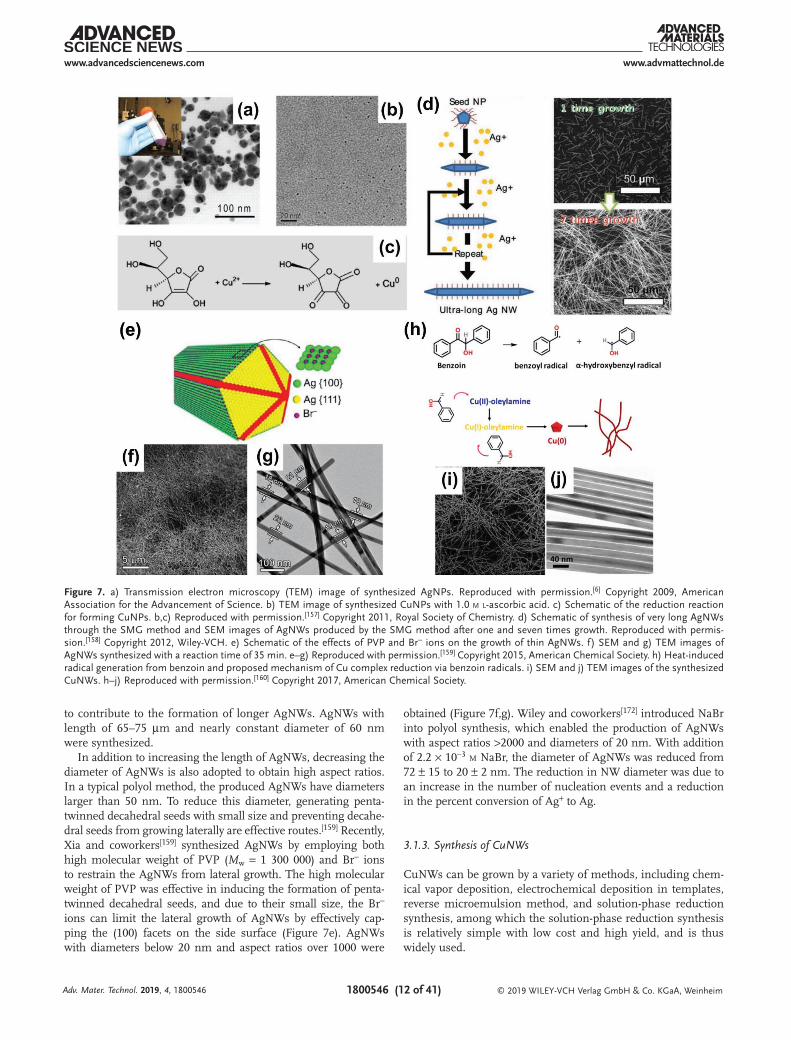
are formed from ionic precursors (e.g., AgNO3, CH3COOAg, CuCl2, Cu(NO3)2) by reaction with proper reducing agents (e.g., diethanolamine, monoethanolamine, formaldehyde, sodium borohydride, hydrazine, ethylene glycol (EG), oleylamine, ascorbic acid, phenylhydrazine, and tin acetate) in solution with the protection of capping agents (e.g., poly(acrylic acid) (PAA), carboxylic acid, polyvinylpyrrolidone (PVP), dodecanethiol (DT), sodium citrate, sodium dodecyl sulfate, sodium polyacrylate, oleylamine, and hexadecylamine).[6,51,145–156] Using wet chem-istry process, the average size, size distribution, and stability of the NPs can be controlled by varying the experimental param-eters during the synthesis. For example, using an aqueous system that contains AgNO3 as the Ag precursor, poly(acrylic acid) as the capping agent, and diethanolamine as the reducing agent, AgNPs with a mean particle size of 20 ± 5 nm and a size distribution between 5 and 50 nm were prepared (Figure 7a).[6] Using an aqueous system that contains CH3COOAg as the Ag precursor, poly(acrylic acid) sodium salt as the capping agent, and ascorbic acid as the reducing agent, AgNPs with an average particle size of 10 nm were prepared.[153] As ascorbic acid could give enough reducibility to convert Cu2+ into CuNPs, using ascorbic acid as both reducing agent and capping agent, CuNPs with diameter of ≈1.5 nm were synthesized by reducing CuCl2 in aqueous solution (Figure 7b,c).[157]
3.1.2. Synthesis of AgNWs
Synthesis of AgNWs has been reported using a number of methods, such as polyol method, microwave-assisted method, UV irradiation method, and template method.[161,162] Out of the various methods, the polyol method is relatively simple with low cost and high yield, hence the most promising route to produce AgNWs. In the polyol process, metallic precursors (e.g., AgNO3) are reduced by a polyol (e.g., EG) in the presence of PVP.[163,164] Different additives, such as PtCl2, AgCl, NaCl, FeCl3, and CuCl2, are often employed, resulting in rapid forma-tion of AgCl nanocubes. Such nanocubes induce the heteroge-neous nucleation of metallic Ag on their surfaces, and AgNWs subsequently grow from the nucleation sites.[165,166] AgNWs are typically grown with diameters of 50–200 nm and lengths of 1–20 µm.[167] The diameter and the aspect ratio of AgNWs are two key structural parameters to influence the optical transmit-tance and sheet resistance of printed/coated AgNW patterns.[168]
To increase the length of AgNWs, which means increasing the aspect ratio of AgNWs, modified polyol methods have been adopted. Ko and coworkers developed a successive multistep growth (SMG) method for very long AgNWs (Figure 7d), where AgNO3 was reduced repeatedly in EG in the presence of PVP. It was demonstrated that AgNWs continued to grow through successive multistep growth as long as Ag ion–rich conditions were maintained continuously. The average length and diam-eter after seven reduction steps of AgNO3 were reported to be 96.1 µm and 160 nm, respectively.[158,169,170] Jiu et al.[171] reported one-pot reaction by adding all agents (EG, PVP, AgNO3, and FeCl3) at room temperature and reacting at a lower tempera-ture of 130 °C for 5 h, which contributed to the nucleation and growth of Ag nuclei during the same stage. In addition, low temperatures and long reaction times also have been confirmed
Adv. Mater. Technol. 2019, 4, 1800546
www.advancedsciencenews.com
© 2019 WILEY-VCH Verlag GmbH & Co. KGaA, Weinheim1800546 (12 of 41)
www.advmattechnol.de
to contribute to the formation of longer AgNWs. AgNWs with length of 65–75 µm and nearly constant diameter of 60 nm were synthesized.
In addition to increasing the length of AgNWs, decreasing the diameter of AgNWs is also adopted to obtain high aspect ratios. In a typical polyol method, the produced AgNWs have diameters larger than 50 nm. To reduce this diameter, generating penta-twinned decahedral seeds with small size and preventing decahe-dral seeds from growing laterally are effective routes.[159] Recently, Xia and coworkers[159] synthesized AgNWs by employing both high molecular weight of PVP (Mw = 1 300 000) and Br− ions to restrain the AgNWs from lateral growth. The high molecular weight of PVP was effective in inducing the formation of penta-twinned decahedral seeds, and due to their small size, the Br− ions can limit the lateral growth of AgNWs by effectively cap-ping the (100) facets on the side surface (Figure 7e). AgNWs with diameters below 20 nm and aspect ratios over 1000 were
obtained (Figure 7f,g). Wiley and coworkers[172] introduced NaBr into polyol synthesis, which enabled the production of AgNWs with aspect ratios >2000 and diameters of 20 nm. With addition of 2.2 × 10⁻³ m NaBr, the diameter of AgNWs was reduced from 72 ± 15 to 20 ± 2 nm. The reduction in NW diameter was due to an increase in the number of nucleation events and a reduction in the percent conversion of Ag+ to Ag.
3.1.3. Synthesis of CuNWs
CuNWs can be grown by a variety of methods, including chem-ical vapor deposition, electrochemical deposition in templates, reverse microemulsion method, and solution-phase reduction synthesis, among which the solution-phase reduction synthesis is relatively simple with low cost and high yield, and is thus widely used.
Adv. Mater. Technol. 2019, 4, 1800546
Figure 7. a) Transmission electron microscopy (TEM) image of synthesized AgNPs. Reproduced with permission.[6] Copyright 2009, American Association for the Advancement of Science. b) TEM image of synthesized CuNPs with 1.0 m l-ascorbic acid. c) Schematic of the reduction reaction for forming CuNPs. b,c) Reproduced with permission.[157] Copyright 2011, Royal Society of Chemistry. d) Schematic of synthesis of very long AgNWs through the SMG method and SEM images of AgNWs produced by the SMG method after one and seven times growth. Reproduced with permis-sion.[158] Copyright 2012, Wiley-VCH. e) Schematic of the effects of PVP and Br− ions on the growth of thin AgNWs. f) SEM and g) TEM images of AgNWs synthesized with a reaction time of 35 min. e–g) Reproduced with permission.[159] Copyright 2015, American Chemical Society. h) Heat-induced radical generation from benzoin and proposed mechanism of Cu complex reduction via benzoin radicals. i) SEM and j) TEM images of the synthesized CuNWs. h–j) Reproduced with permission.[160] Copyright 2017, American Chemical Society.

www.advancedsciencenews.com
© 2019 WILEY-VCH Verlag GmbH & Co. KGaA, Weinheim1800546 (13 of 41)
www.advmattechnol.de
In the solution-phase reduction synthesis, Cu ion precursors are reduced by reducing agents in the presence of organic addi-tives. Two general approaches have been employed to synthe-size CuNWs: ethylenediamine (EDA)-mediated synthesis and alkylamine-mediated synthesis. The EDA-mediated synthesis of CuNWs was first reported by Zeng and coworkers[173] and modified by Wiley and coworkers,[174] who magnified the reac-tion by a factor of 100. In a typical synthesis process, Cu(II) ions are reduced by hydrazine (N2H4) in a basic solution con-taining EDA as the capping agent. The resulting CuNWs are 90 ± 10 nm in diameter and 10 ± 3 µm in length. Their more recent work revealed the growth mechanism of CuNWs in the EDA-mediated approach. EDA is a facet-selective promoter of Cu atomic addition to the (111) facets at the end of a CuNW rather than a capping agent stabilizing the (100) facet to inhibit the lateral growth.[175] Using the alkylamine-mediated approach, high-quality and uniform CuNWs can also be synthesized. For example, Zhang et al.[176] synthesized ultralong single-crys-talline CuNWs with diameter of 78 nm and lengths of tens to hundreds of micrometers up to several millimeters in liquid-crystalline medium of hexadecylamine and cetyltrimethylam-monium bromide (CTAB). Interestingly, the whole synthesis process was carried out in nonaqueous media, which effectively decreased the aggregation of the CuNWs. It should be noted that shorter chain length of alkylamines can increase the rate of Cu reduction and produce higher yields and longer CuNWs.[177]
Synthesis of CuNWs using carbon organic radicals as reduct-ants was also reported by Yang and coworkers.[160] As shown in Figure 7h, upon heating, benzoin was decomposed into benzoyl radical and hydroxybenzyl radical. Due to the conjuga-tion of the benzene ring, these radicals were relatively stable in an air-free atmosphere, being capable of reducing metal complex in solution. Specifically, Cu(II) precursors were first reduced to Cu(I) at low temperature of 120 °C, which were further reduced to Cu at high temperature of 185 °C. With the aid of oleylamine, Cu nucleation preferred a fivefold twinned structure and CuNWs possessed a length of up to 20 µm and a diameter of 18.5 ± 3.5 nm (Figure 7i,j). More recently, this group also used the same method to synthesize AgNWs with diameter as thin as 13 nm and aspect ratio up to 3000.[178]
To reduce the corrosion/oxidation of CuNWs in air, a pas-sivation layer of carbon and metal (e.g., Ni, Ag, Au, and Pt) has been introduced during the CuNW synthesis process.[179–181]
3.2. Formulation of Metal Nanomaterial–Based Printable Inks
In general, the method of formulating metal inks is to disperse the synthesized NPs/NWs in proper solvents containing some specific binders and additives. For example, to obtain CuNP ink for screen printing, CuNPs, EG, and PVP were ball-milled together for 4 h before use.[182] To obtain water-based AgNW ink for screen printing,[19] a mixture of (hydroxypropyl)methyl cellu-lose (HMC), fluorosurfactant (Zonyl FS-300), and antifoaming agent (Defoamer MO-2170) was employed as the organic binder/additives. HMC acted as a rheological agent to provide suitable thixotropic behavior. The hydroxyl groups in HMC can bond strongly on the surface of AgNWs and thus work as a dis-persive agent to achieve good dispersion of AgNWs and provide
dispersion stability. Zonyl FS-300 decreased surface tension of the water-based ink, promoting the substrate wettability during printing. Defoamer MO-2170 provided efficient defoaming per-formance in aqueous printing inks and helped prevent foam formation during mechanical agitation. The AgNW ink, which contained a low solid content of 6.6 wt%, a viscosity as high as 405.8 Pa s at 0.1 s−1 shear rate, and appropriate rheological behavior, was suitable for screen printing. In another example of AgNW ink for EHD printing, AgNWs were dispersed in poly(ethylene oxide) (PEO) aqueous solution.[43,183] PEO was used to assist ink formulation for the following reasons: i) high molecular weight PEO can increase the viscosity of the ink dra-matically, and provide thixotropic behavior for the ink; ii) PEO can function as a dispersive agent to improve dispersion of AgNWs as the hydroxyl groups can bond with the surface of the AgNWs; and iii) PEO can precipitate together with AgNWs after printing to generate solid composite sediments, which was con-ducive to forming a uniform, continuous pattern.[184] Similar ink formulation can also be used for preparing gravure-printed AgNW ink.[185] In order to form a crack-free dense microstruc-ture that adheres well to substrates, nano- or micrometer-sized glass frits were often applied to the AgNP or Ag flake ink.[186,187]
3.3. Formulation of Carbon Nanomaterial–Based Printable Inks
Due to the low dispersibility of graphene and CNTs in a variety of solvents, it is a challenge to fabricate printable carbon nano-material inks with high load density against aggregation and precipitation.[188]
Liquid-phase exfoliation, either by sonication-assisted exfo-liation or by shear force–assisted exfoliation, has been well studied in the past several years to obtain high-quality graphene due to its simplicity and low cost.[189,190] For example, Coleman and coworkers first developed a simple method to directly exfo-liate graphite to monolayer or few-layer graphene in various solvents (e.g., N-methylpyrrolidone (NMP) and N,N-dimeth-ylformamide (DMF)) using a normal ultrasonication bath. To improve exfoliating efficiency, a microfluidization-assisted method was developed recently, where high pressure forces the graphite containing solvents to pass through a microchannel to provide a shearing speed >108 s−1.[191] Typically, bulk graphite can be exfoliated to be thin graphene flakes with 100% yield, including 4% of the flakes with thickness <4 nm and 96% between 4 and 70 nm.
For printable graphene ink, two general strategies have been demonstrated: i) dispersing graphene directly in solvents (e.g., NMP, water/ethanol, isopropyl alcohol (IPA)) without addi-tives, and ii) stabilizing graphene in a broader range of organic solvents (e.g., terpineol, dipropylene glycol) using additives (e.g., ethyl cellulose (EC) and PVP).[42,192–194] For example, to synthesize graphene ink for inkjet printing, the graphene ink was prepared by first exfoliating graphite flakes in DMF, and exchanging DMF with terpineol to distil due to the large differ-ence between their boiling points. To prevent graphene sheet aggregation during DMF evaporation, a certain amount of EC was added into the graphene/DMF suspension as the stabilizer. The graphene concentration could be up to ≈1 mg mL−1. Finally, the EC can be effectively removed through a post-printing
Adv. Mater. Technol. 2019, 4, 1800546
www.advancedsciencenews.com
© 2019 WILEY-VCH Verlag GmbH & Co. KGaA, Weinheim1800546 (14 of 41)
www.advmattechnol.de
thermal sintering at 300–400 °C in air for 1 h.[193] Recently, a water-based and inkjet-printable 2D crystal ink was put forward by Casiraghi and coworkers.[42] Liquid-phase exfoliation of gra-phene was done in water by adding small amount of 1-pyrene-sulfonic acid sodium salt as the exfoliating and stabilizing agent. After the exfoliation process, a low concentration of Triton X-100 was chosen as surface tension modifier to avoid disrupting the electrostatic stabilization of graphene flakes in the water-based ink. Most notably, by adding propylene glycol as cosolvent resulted in an increase of viscosity leading to improved printing reliability and these inks are also biocompatible.
Graphene oxide (GO), which is typically obtained by oxida-tion of graphite in the presence of strong acids and oxidants, can be easily dispersed in water and other organic solvents due to the presence of the oxygen functionalities. However, harsh post-printing treatments (i.e., chemical reduction and thermal sintering) are required to obtain reduced GO (RGO), which often leads to more defects and poor conductivity compared with pristine graphene. This makes GO less appealing to elec-tronic applications.[58,195]
There are three major approaches to disperse CNTs: i) dispersing CNTs in neat organic solvents, or superacids; ii) dispersing CNTs in aqueous media by using dispersing agents, such as surfactants or polymers; and iii) modification of CNTs with functional groups, which helps to disperse CNTs in solution.[196] For example, CNT ink was screen printed by using sodium dodecyl sulfate, PVP, and ethanol as dispersant, binder, and solvent, respectively.[197] To make MWNTs dispersible in water, MWNTs were first refluxed in HNO3 to produce car-boxyl, hydroxyl, and carbonyl groups at the defect sizes of the nanotubes. Then these hydroxyl and carbonyl groups were fur-ther oxidized by KMnO4 solution to achieve additional carboxyl groups. After sonicating and centrifuging functionalized nano-tubes, the supernatant solution containing CNTs with length of 1–5 µm was used as ink for inkjet printing.[198]
4. Printing Conductive Nanomaterial Inks
4.1. Inkjet Printing
Inkjet printing of metal NP inks, especially AgNP ink, is widely used for printing circuits and conductors, which form the basis of printed electronic devices.[3]
Paper-based substrates have recently attracted increasing research and commercial interests for PE due to their natural abundance, light weight, renewability, mechanical flexibility, and nontoxicity over their counterparts.[199–202] Coffee ring effect is often undesired but does exist during inkjet printing process. However, researchers have exploited coffee ring effect to achieve highly conductive patterns in the past few years.[79] Inkjet printing of AgNWs, graphene, and CNTs has also attracted extensive academic interest.
In this part, we will focus on the advances in inkjet printing of metal NP inks on paper substrates; then the progress in forming conductive films using the coffee ring effect by inkjet printing will be presented; finally, we will discuss the recent progress of inkjet printing of AgNW inks and carbon nanoma-terial–based inks.
4.1.1. Inkjet Printing of Conductive Patterns on Paper Substrates
Paper substrates, especially photopaper (inkjet paper) that is glossy, coated on one or both sides, and has fast-drying proper-ties, have been used in PE by inkjet printing. Using an inex-pensive commercial color printer (Epson Stylus Photo R230), Song and coworkers inkjet printed water-based AgNP ink on photopaper to fabricate conductive circuits.[51] Viscosity and surface tension of the AgNP inks with different Ag concen-trations were characterized prior to printing to make sure the Z values fell within the range of 1–10. The resistivity of the printed Ag patterns was decreased to 3.7 µΩ cm by increasing the sintering temperature to 180 °C. It should be noted that even by drying the Ag patterns at room temperature, a rela-tively low resistivity (8.0 µΩ cm) can be obtained on the photo-paper. However, such a phenomenon did not happen on sticky note paper or copy paper.[203] The large differences of resist-ance on different papers can be explained by the substantial differences in the surface coating properties of the different papers.[204,205]
One advantage with paper substrate over plastic substrate is that the coffee ring effect is less pronounced due to the liquid absorption that competes with the initial spreading and the final evaporation.[206] However, wetting has the effect of dis-persing inks deposited on the paper substrate, and lowering the printing resolution. The physical and chemical proper-ties of paper substrates may be altered by chemical additives or changes in materials and processes.[207–209] Therefore, it is possible to tailor the paper or coating, adapting it to a specific functional ink. Whitesides and coworkers modified the surface free energy of Canson tracing paper using a fast vapor-phase treatment with organosilane.[210] Without treatment, water droplets were found to immediately wick into the paper; with treatment of decyltrichlorosilane, the contact angle of water droplet was enlarged to 128 ± 4°, which transformed the paper into a material that is omniphobic. As a result, the lateral reso-lution of printed lines decreased from 585 ± 87 to 90 ± 5 µm (Figure 8a,b).
4.1.2. Inkjet Printing of Conductive Patterns Using Coffee Ring Effect
By controlling the migration of AgNPs within the evaporating droplets by regulating the wettability of the substrates, a variety of complex structures, such as a new type of TCFs containing rings,[85] holes,[211] and 2D reticular structures,[84,212] were fab-ricated by inkjet printing. Magdassi and coworkers pioneered this method. For example, as shown in Figure 8c, inkjet-printed AgNP droplets formed self-assembled rings due to the coffee ring effect. The rims of the rings consisted of self-assembled, closely packed AgNPs. Width and height of the rims were less than 10 µm and 300 nm, respectively, while diameter of the ring was about 150 µm. To obtain transparent conductive patterns, a 2D array of overlapping AgNP rings was formed (Figure 8d). The whole interconnected ring array presented a high trans-parency of 95% and a low sheet resistance of 4 Ω sq−1.[211] The same group also fabricated arrays of connected “coffee rings” composed of CNTs by inkjet printing, and after post-printing
Adv. Mater. Technol. 2019, 4, 1800546

www.advancedsciencenews.com
© 2019 WILEY-VCH Verlag GmbH & Co. KGaA, Weinheim1800546 (15 of 41)
www.advmattechnol.de
treatment with hot nitric acid, the transparent CNT patterns had a sheet resistance of 156 Ω sq−1 and transparency of 81%.[213]
Note that if the contact lines of inkjet-printed droplets are inhibited from dewetting on the substrate, a long stable rivulet with two parallel contact lines can form. Pinned contact lines and edge-enhanced evaporation of the solvent caused the NPs to deposit along the rivulet periphery forming twin continuous NP lines with minimal deposition between the lines.[212] Elongated ellipse-shaped patterns can be formed based on this effect, while the NPs are accumulated in narrow parts of the printed lines. The width of the line composed of AgNPs was 5–10 µm that resulted in a transparent pattern.[84] These ellipse-shaped patterns were interconnected in the form of a grid and had a transparency of 92% with line resistivity in the range of 2.61 × 10⁻³ to 5.76 × 10⁻⁴ Ω cm when thermally sintered at 160–200 °C for 2 h (Figure 8e–g).
4.1.3. Inkjet Printing of AgNW Networks
Inkjet printing of AgNWs is extremely challenging due to the length of AgNWs that is usually tens of micrometers, which can easily cause clogging of the nozzle. Several attempts have been made to achieve conductive patterns.[39,214–217] The first attempt to inkjet printing AgNW ink was to add AgNWs to the AgNO3 ink to lower the concentration of AgNO3 and increase
the viscosity of the ink.[214] Continuous and smooth Ag lines with a resistivity of 7.31 × 10⁻⁵ Ω cm were achieved on a flex-ible Kapton substrate after reducing by EG vapor for 1 h at 200 °C. Recently, Coleman and coworkers[39] demonstrated inkjet printing of AgNWs on flexible polyethylene terephtha-late (PET) substrates. AgNWs were first reduced to 2.2 µm in mean length by sonication in a low-power ultrasonic bath for 3 h, and then cosolvents of IPA and diethylene glycol (DEG), which could suppress the satellite droplets during printing, were added to form AgNW ink. To control solvent evaporation during and after deposition, an intermediate drying step was introduced during a print session using processing tempera-ture no more than 110 °C. The inkjet-printed lines, consisting of random AgNWs and 1–10 mm in width and 0.5–2 µm in thickness, displayed sheet resistance as low as 8 Ω sq−1 and conductivity as high as 105 S m−1. To improve printability and to reduce post-treatment temperature, a solvent replace-ment approach was used.[215] An aqueous AgNW ink was pre-pared by replacing IPA with water to form a water-based ink. Such a AgNW ink (length of AgNWs: 20–50 µm) fulfilled the minimum requirement of regular inkjet printing due to low sedimentation rate and avoidance of potential clogging near the printing nozzle. Very recently, AgNWs with average length of 3.6 µm were dispersed in pure ethanol to form ink with solid content of 10 mg mL−1 and then inkjet printed on a PET substrate (Figure 9a). Such an ink formulation can improve the printing results owing to two features: i) fast evaporation
Adv. Mater. Technol. 2019, 4, 1800546
Figure 8. a) Images of 10 µL drops of water on a series of Canson tracing papers, modified with different organosilanes, and their corresponding static contact angles. b) Optical images of Ag lines printed on the corresponding Canson tracing paper substrates in part (a). a,b) Reproduced with permis-sion.[210] Copyright 2014, Wiley-VCH. c) SEM images and height profile of a printed ring pattern. d) Array of interconnected rings. c,d) Reproduced with permission.[85] Copyright 2009, American Chemical Society. e) Schematic illustration of inkjet printing of AgNP patterns induced by the coffee ring effect. f) Optical image of a reticular conductive pattern based on printed coffee ring lines of AgNPs. g) Transmittance of a glass substrate with the reticular conductive pattern. e–g) Reproduced with permission.[84] Copyright 2013, Wiley-VCH.

www.advancedsciencenews.com
© 2019 WILEY-VCH Verlag GmbH & Co. KGaA, Weinheim1800546 (16 of 41)
www.advmattechnol.de
of ethanol; and ii) high concentration of AgNWs in the ink. Coffee ring effect can be effectively inhibited (Figure 9b) and only four printing passes are needed to create AgNW percola-tion to reduce printing time.[218]
4.1.4. Inkjet Printing of Carbon Nanomaterials
The first demonstration of inkjet-printed graphene electronics was reported by Ferrari and coworkers,[36] where graphene dis-persed in pure solvent of NMP was used to print transistors. The resultant inkjet-printed film showed a sheet resistance down to 30 kΩ sq−1 and ≈80% transmittance at the wavelength of 550 nm. After that, improvements have been achieved by different research groups. For example, Hersam and cow-orkers demonstrated an inkjet-printed graphene ink using cyclohexanone/terpineol as solvents and EC as binder.[219,220] Such an ink supported a highly controllable, spatially uniform deposition of graphene with linewidth of 60 µm and electrical conductivity of 25 000 S m−1. To further render the graphene with high electrical conductivity, mechanical durability, and environmental stability, the same group introduced nitrocellu-lose as binder to the ink.[61] The graphene films exhibited elec-trical conductivity up to 40 000 S m−1 following 350 °C thermal sintering. In addition, thermal decomposition of nitrocellu-lose resulted in robust amorphous carbon residues, yielding the inkjet-printed graphene patterns resilient to a range of mechanical and environmental stresses (Figure 9c,d). Recently, water-based and biocompatible graphene ink was used to print electronic devices.[42] As shown in Figure 9e, Nobel medal was printed with water-based graphene ink on PEL P60 paper under ambient conditions. The relationship between sheet
resistance and droplet spacing and printing passes is shown in Figure 9f.
Several studies have been reported on inkjet printing of CNTs to obtain conductive patterns. By printing water-based SWNT ink onto paper and plastic substrates, patterns with sheet resistance of ≈40 000 Ω sq−1 were obtained.[198] By opti-mization of the printing parameters, inkjet-printed MWNT thin film electrodes showed conductivity up to 30 S cm−1 without the need of any post-printing treatment.[221]
4.2. Electrohydrodynamic Printing
EHD printing can overcome limitations of inkjet printing in terms of the size of nozzle arrays, the viscosity of ink, and the droplet size.[222,223] EHD printing is an effective way to pattern high-resolution patterns.[224–229] Rogers and cow-orkers first reported EHD jet printing SWNT dots with diameter of ≈8 µm using nozzles with internal diameter of 30 µm. Furthermore, by using much smaller nozzle (diam-eter ≈2 µm) and printing speed (≈20 µm s−1), 2 µm diameter dots were obtained.[32] EHD printing of AgNP inks enables the printed linewidth of less than 10 µm for the Ag grid transparent electrode, which is invisible to naked eyes. After sintering at 200 °C under near-infrared (NIR) light, the EHD-printed transparent electrode with 150 µm Ag grid pitch had a sheet resistance of 4.87 Ω sq−1 and transmittance of 81.75%.[224] Large-scale patterns of RGO with complex geom-etries (e.g., alphabetic letters) with linewidth of ≈5 µm can be obtained.[230] Recently, much attention has been paid to printing 3D conductive structures and AgNW networks using EHD printing.
Adv. Mater. Technol. 2019, 4, 1800546
Figure 9. a) Optical image of inkjet-printed AgNW lines on a coated PET substrate. b) SEM image of a printed AgNW line in the edge area. a,b) Reproduced with permission.[218] Copyright 2018, American Chemical Society. c) A series of images showing the water sonication for graphene/EC and graphene/NC. d) Change in electrical resistance following the damp heat test, 312 h at 85 °C and 85% relative humidity, for graphene/EC and graphene/NC films on polyimide and glass. c,d) Reproduced with permission.[61] Copyright 2017, American Chemical Society. e) Nobel medal printed with water-based graphene ink on PEL P60 paper. f) Sheet resistance as a function of the number of printed passes for graphene lines (2 cm length) printed on PEL P60 paper with a drop spacing of 40 µm (red points) and 25 µm (blue points). Inset: Optical images of printed lines with 1, 5, 10, 15, and 20 printed passes. e,f) Reproduced with permission.[42] Copyright 2017, Springer Nature.

www.advancedsciencenews.com
© 2019 WILEY-VCH Verlag GmbH & Co. KGaA, Weinheim1800546 (17 of 41)
www.advmattechnol.de
4.2.1. Electrohydrodynamic Printing of Complex 3D Structures
EHD printing offers unique potentials for fabricating 3D pat-terns. By controlling the printing and sintering processes, high-aspect-ratio Au and Ag grid transparent electrodes with width of 80–500 nm and height of 0.2–1.5 µm were fabricated with
AuNP and AgNP inks, respectively.[226,227] This EHD printing process demonstrated the capability of printing high-aspect-ratio structures (e.g., nanowalls) with high resolution and low sheet resistance while maintaining the high-level optical transpar-ency. As shown in Figure 10a, after thermal sintering of printed Ag grid at 200 °C, transparent electrode with sheet resistance of
Adv. Mater. Technol. 2019, 4, 1800546
Figure 10. a) EHD nanodrip-printed Ag grid with a pitch of 20 µm and aspect ratio (height to width) of 2.5. Reproduced with permission.[227] Copyright 2016, Wiley-VCH. b) SEM image and schematic of heterogeneous 3D structures with two different materials. The black and white walls are made of anthracene and Ag, respectively. Scale bar: 5 µm. Reproduced with permission.[101] Copyright 2015, Wiley-VCH. c) Schematic of spontaneous nanoscale Joule heating during EHD printing of the high-aspect-ratio 3D structures. d) SEM image of a sub-10 µm 3D pillar with a high aspect ratio of over 35. Scale bar: 10 µm. Inset: Optical image of multiple pillars; scale bar: 30 µm. c,d) Reproduced with permission.[231] Copyright 2017, American Chemical Society. e) Snapshot of a florescence image obtained from the PIV experiment for EHD jet. Schematics showing the hydrodynamic drag force on a AgNW during EHD printing: f) when the axial direction of the Ag NW is parallel to the flow direction, the drag force is minimized; g) when perpendicular, the drag force can compel the Ag NW to rotation. e–g) Reproduced with permission.[183] Copyright 2014, Wiley-VCH. h) Large-scale AgNW pattern printed by EHD printing. Scale bar: 1 cm. i) Two complex AgNW patterns with high resolution. Scale bar: 5 mm. h,i) Reproduced with permission.[43] Copyright 2018, Royal Society of Chemistry.

www.advancedsciencenews.com
© 2019 WILEY-VCH Verlag GmbH & Co. KGaA, Weinheim1800546 (18 of 41)
www.advmattechnol.de
58 Ω sq−1 and optical transmittance of 98% could be obtained. By engineering a perfect balance between the AgNP ink and electro-magnetic (EM) field, Park and coworkers succeeded in releasing ink droplets smaller than the nozzle, thus enabling printing of complex 3D structures with high resolution.[101] In order to apply EHD to 3D printing, a hydrophobic layer was coated on the nozzle to prevent inks from wetting the nozzle sidewall. Fur-thermore, volatile solvents (vapor pressure ≥1 Torr at 25 °C) were used in the ink to facilitate instant drying of the droplet, so that ink droplet can be dried before reaching the substrate, enabling the vertical stacking of ink materials. As shown in Figure 10b, the nanowalls, consisting of Ag and anthracene, could also be sepa-rated to form a square-like 3D pattern. Recently, one-step EHD printing of sub-micrometer-scale 3D structure was developed.[231] By printing low-viscosity AgNP ink (i.e., lower polymer con-centration in the ink formulation), self-sintering of the charged AgNPs during the printing process due to the nanoscale Joule heating was observed (Figure 10c). According to computational simulation, the maximum temperature between NPs can be as high as 800 °C, which was much higher than the melting point of AgNPs (≈150 °C). Thus, the AgNP self-sintering process occurred simultaneously at the interface between the charged AgNPs, forming the aggregated AgNP junction and 3D structures. Sub- micrometer-scale 3D structures were printed with an aspect ratio of 35 using the one-step EHD printing technique (Figure 10d).
4.2.2. Electrohydrodynamic Printing of AgNW Networks
EHD printing has been recently used to print AgNWs.[43,183,232] One work focused on aligning AgNWs at very low NW density (3 mg mL−1).[183] As shown in Figure 10e, from the particle image velocimetry (PIV), the velocity of the jet at the interface was largest while the velocity near the center was relatively slow. Shear stress in the fluid flow can align NWs to be parallel lengthwise to the flow direction (Figure 10f,g). With the combination of the fluid flow and the electric field inside the EHD jet, AgNWs were suc-cessfully aligned and printed. However, due to the low density of the AgNWs, the EHD-printed AgNW lines were not conductive. Our group has demonstrated a high-resolution, large-scale printing of highly conductive AgNWs using EHD printing.[43] By adjusting several ink and printing parameters, e.g., ink viscosity, AgNW con-centration, stand-off distance, printing speed, voltage, nozzle size, and pressure, complex patterns can be deposited on a variety of substrates including plastics, elastomers, and papers (Figure 10h,i). The printed AgNWs showed an electric conductivity as high as ≈5.6 × 10⁶ S m−1 with AgNW concentration of 15 mg mL−1.
EHD spraying, which uses electrical field for liquid atomi-zation, is another approach to deposit AgNW patterns. AgNW transparent electrode[233] and AgNW-embedded PEDOT:PSS hybrid thin films[234] were printed using a commercial EHD spraying machine.
4.3. Aerosol Jet Printing
As a direct-writing and noncontact depositing technique, aer-osol jet printing is mainly used to print conductive circuits and components on various substrates.
4.3.1. Aerosol Jet Printing of Metal Nanomaterials
Ag interdigitated electrodes were deposited onto printed cir-cuit boards by aerosol jet printing of AgNP ink. The lines were 20–50 µm in width and 8–10 µm in thickness with electrical resistivity of 4–12 µΩ cm after thermal sintering at 200 °C.[235] By adding proper graphene or CNTs into AgNP ink, the con-ductivity of the printed lines increased with graphene or CNTs serving as bridges to cross the defects/granular bounda-ries.[236,237] Moreover, by reducing the atomizer flow rate, which means increasing FR, relatively high resolution of Ag penrose tiles with linewidth of ≈20 µm was obtained.[118]
Due to the relatively high standoff of the printer head above the substrate and long focal length of the material beam exiting the nozzle, aerosol jet printing is an ideal solution to printing on nonplanar surfaces.[115,120,238,239] For example, Ag intercon-nects with 22 µm in width were printed on the outer sidewall of hollow plastic pillar.[115] In addition to aerosol jet printing AgNWs to flat plastic substrate,[240,241] AgNW networks could also be printed on rough, nonuniform 3D-printed objects with aerosol-assisted atmospheric pressure plasma-based printing.[120] Deposition of conductive traces at room temperature was real-ized with the assistance of plasma, and AgNW patterns formed a highly interlinked network covering both shallow and deep gaps between the plastic fibers of the 3D-printed nonplanar sub-strates. Besides printing on 3D nonplanar substrates, aerosol jet printing can also be used to build 3D structures. Recently, AgNPs dispersed in a mixture of water and EG were deposited by aerosol jet printing to fabricate 3D scaffold structures with hierarchical porosity (Figure 11a,b). The structural features are shown spanning over five orders of magnitudes in length scale. The internal porosity and surface topography of the truss ele-ments of the scaffolds can be controlled by varying sintering conditions (e.g., sintering profile and/or power source).[242]
4.3.2. Aerosol Jet Printing of Carbon Nanomaterials
To obtain proper graphene ink for printing, the ink formulation consisting of solvents of cyclohexanone/terpineol and binder of EC was prepared. After printing the ink on a hydrophobic Si/SiO2 substrate, the width of the printed graphene intercon-nects was down to 10 µm.[244]
For electronic devices, understanding power dissipation in nanoscale structures is of great importance. Recently, the power dissipation and electrical breakdown in aerosol jet printed gra-phene interconnects were investigated. Microstructures and substrate properties played key roles in the power dissipation and electrical breakdown of the graphene interconnects. Elec-trical breakdown was likely due to the high porosity causing trapped gases and solvents within interconnects, as well as weak interlayer bonding of graphene flakes. Furthermore, power dissipation was dominated by the graphene interconnect mor-phology for substrates with high thermal conductivity (e.g., Al2O3 substrate); however, power dissipation can be limited by polymer substrates with low thermal conductivity (e.g., poly-imide substrate).[245] Aerosol jet printing has been proved to be a suitable method for printing large-area, CNT-based transistors on flexible substrate, which will be summarized in Section 6.
Adv. Mater. Technol. 2019, 4, 1800546

www.advancedsciencenews.com
© 2019 WILEY-VCH Verlag GmbH & Co. KGaA, Weinheim1800546 (19 of 41)
www.advmattechnol.de
4.4. Slot Die Coating
By coating the AgNP ink onto the flexible substrate using the slot die method followed by a drying process using a NIR lamp, piezoresistive strain sensors were fabricated.[122] The com-parison to commercial products shows a 40% increase in the gauge factor. Slot die coating can be used for coating AgNP inks to form electrode layers, such as the back electrode for solar cells.[246] The ink properties and coating parameters can be optimized to achieve a satisfying layer quality.
4.4.1. R2R Slot Die Coating TCFs
Recently, several groups have reported printing of highly TCFs consisting of AgNWs using R2R slot die coating. 400 mm wide AgNW network film was prepared on a PET substrate. By controlling the flow rate of the shear-thinning AgNW ink, AgNW percolating network films with sheet resistance of 30–70 Ω sq−1, optical transmittance of 89–90%, and haze of 0.5–1% were obtained, which could be used for low-cost flex-ible screen panels.[247] Furthermore, to enhance the adhesive strength between AgNW network film and PET substrate, an overcoating layer of acrylic resin was applied on the substrate before slot die coating process.[248]
In addition to a single layer of AgNWs, formation of hybrid structures with PEDOT:PSS, graphene, and CNTs utilizing R2R slot die coating has also been demonstrated for large-area
applications.[249–252] To improve electrical conductivity of the printed film, PEDOT:PSS conductive polymer inks were modi-fied by adding AgNWs in solid contents of 10–20 wt%.[250] Highly uniform films with optical transmission higher than 80% and sheet resistance lower than 40 Ω sq−1 were obtained after slot die coating of the ink on a PET substrate. A large-area CNT/AgNW hybrid layer was coated using a R2R slot die coating system.[251] Films with width of 250 mm were continu-ously coated and showed good uniformity with average surface roughness of 19.02 nm, sheet resistance of 102 Ω sq−1, and transmittance of 87.03%. In other cases, carbon conductive materials in combination with PEDOT:PSS film have also been achieved by R2R slot die coating.[253]
4.5. Screen Printing
Screen printing is a potential technique for mass production of printed electronics and has been widely employed to produce conductive electrodes.
4.5.1. Screen Printing of Metal Nanomaterials
Screen printing metallization is the most widely used con-tact formation technique for commercial Si solar cells.[254] Ag flake is the most mature technology and remains the most widely utilized technique currently used in the manufacturing
Adv. Mater. Technol. 2019, 4, 1800546
Figure 11. a) A simplified free-body diagram of a critical droplet at the edge of a structure and the illustration of a designed experiment to verify the model for aerosol jet printing. b) SEM image of a petal-shaped structure. a,b) Reproduced with permission.[242] Copyright 2017, American Association for the Advancement of Science. c) Schematic of the interface morphology evolutions and associated adhesion mechanisms of AgNP film. Reproduced with permission.[243] Copyright 2015, Wiley-VCH.

www.advancedsciencenews.com
© 2019 WILEY-VCH Verlag GmbH & Co. KGaA, Weinheim1800546 (20 of 41)
www.advmattechnol.de
of conductive elements.[255,256] However, these flakes or parti-cles do not allow high-resolution printing with the linewidth smaller than 70 µm, which results in high shadow losses.[254] To improve the resolution of screen-printed Ag patterns, several methods have been employed: i) increasing the substrate tem-perature to reduce the deposited ink quantity and spreading, ii) modifying the mesh surface to control the adhesion of the ink on the mesh, and iii) decreasing width of the stencil opening.[254,257,258] Recently, highly loaded AgNP ink (77 wt%) using water and EG as cosolvents and narrow openings of silicon stencils ranging from 5 to 50 µm in width was applied to obtain Ag lines with linewidth as small as 22 µm and resis-tivity of 5.5 µΩ cm. The resistivity was lower than that of screen-printed Ag flake patterns (typical resistivity values of 18–25 µΩ cm).[258] By dispersing CuNPs in EC and terpineol, highly viscous Cu paste was screen printed on PET substrate. After thermal sintering the printed film at 120 °C with a con-tinuous purge of H2 and N2 in a ratio of 5:95 for 3 h, electrical resistivity was 58.7 µΩ cm.[259]
Much attention has also been paid to synthesize AgNW inks for screen printing.[19,260] The minimum feature size of 50 µm was achieved for the printed linewidth and spacing between the lines.[19] The initial conductivity of the printed AgNW lines was measured as high as 4.67 × 10⁴ S cm−1; voids in the printed lines were believed to be the main reason for the decrease in the electrical conductivity as the linewidth increased.
Due to the significant technological importance of screen-printed Ag nanomaterials in printed electronics, it is essential to investigate the adhesion mechanisms between Ag film and substrate. Interfacial fracture energy is typically measured in order to understand the adhesion mechanism, which, in the case of Ag patterns on Si substrate,[243] was influenced by two main factors: interfacial surface roughness and amount of organic residues at the interface. As shown in Figure 11c, the maximum fracture energy was obtained at the optimal sin-tering temperature of 250 °C due to the significant increase in surface roughness and the presence of sufficient amount of organic residues at the interface. These results can be applied to printed Ag films to enhance and control the interfacial frac-ture energy for mechanically robust electronic applications.
4.5.2. Screen Printing of Carbon Nanomaterials
Huang and coworkers first demonstrated a screen-printed RGO ink by dispersing RGO sheets in terpineol with EC as binder, which can be used as counter electrodes for dye-sensitized solar cells. However, harsh thermal sintering at 400 °C was used to burn off the binder to obtain desirable conductivity, which inevitably affected the adhesive properties of the printed pat-terns.[35] In addition to EC, other polymers can be added to graphene as binder considering the practical application. For example, for screen printing graphene-based electrodes for supercapacitors, polyaniline (PANI) was added into nanog-raphene platelets (NGPs). On one hand, NGPs can serve as a stable conductive network for PANI; on the other hand, PANI can serve as a spacer to further separate NGP neighboring sheets and enhance the finial capacity through fast faradaic pseudocapacitance effects.[261] In another example, using water
as solvent and acrylate as thickening agent, GO ink can be screen printed on woven cotton textiles to fabricate electrodes for supercapacitor.[262]
To gelate of graphene dispersion for screen printing process, PVP and polyvinyl acetate were used as binders, and dipro-pylene glycol as solvent. The printed linewidth can be down to 40 µm.[195] In another example, high-quality graphene pat-terns with resolution of 40 µm were also achieved by screen printing, resulting from the fine line opening as well as the tuned viscosity of the graphene inks. The graphene patterns exhibited high electrical conductivity of ≈1.86 × 10⁴ S m−1 and outstanding mechanical flexibility on polyimide films.[8]
4.6. Gravure Printing
Gravure printing is an attractive technique for patterning high-resolution features at high speed.
4.6.1. Gravure Printing of Metal Nanomaterials
Like screen printing, Ag flake ink and AgNP ink are often used for gravure printing. The differences in ink characteristics lead to differences in printability and electrical performances of the two inks.[133,263,264] Gravure-offset R2R-printed AgNP film on PET substrate was sintered with a rapid laser sintering process in ambient conditions as an alternative to the conventional thermal sintering process. The laser sintered AgNP film exhib-ited superior electrical and mechanical properties, with fast sintering time and no damage to the substrate.[265–267] Very few studies have been reported for gravure printing of CuNP inks. CuNPs were added to a mixture solution of EG, glycerin, and additives. Under vigorous stirring and ultrasonication, the ink in the form of Cu paste can be gravure printed on polyimide film. After sintering at 300 °C for 1 h in the nitrogen, the resis-tivity can be down to 109 µΩ cm.[268]
Gravure printing of AgNWs has received much atten-tion.[185,269–272] AgNW network was gravure printed onto PET substrate using copper-based engraved plates with etched trenches. Conductive lines with different linewidths were fabricated by adjusting printing speeds and pressures.[270] For example, under printing pressure of 174 kPa, a linewidth of 230 ± 2 µm with smooth edges was obtained at 12 cm s−1. Recently, our group has reported gravure printing of AgNW inks on PET substrate.[185] By tailoring the ink properties and printing conditions to make the Ca number ≈1, our group reported high-resolution, highly conductive AgNW patterns in large areas by gravure printing, with linewidth of 50 µm, line spacing of 100 µm, and conductivity as high as 5.34 × 10⁴ S cm−1, which demonstrated the excellent potential of gravure printing for developing large-area flexible electronics based on AgNWs. Moreover, AgNWs were better aligned along the printing direction for smaller linewidth, which may contribute to the observed increase in electrical conductivity (Figure 12a,b).
The use of high-speed, R2R gravure printing was investigated for depositing AgNW-based TCFs.[269,271] The AgNW network thickness on the substrate can be easily controlled by gravure coater rolling speed and gravure cell size. Then, the wet coating
Adv. Mater. Technol. 2019, 4, 1800546

www.advancedsciencenews.com
© 2019 WILEY-VCH Verlag GmbH & Co. KGaA, Weinheim1800546 (21 of 41)
www.advmattechnol.de
of AgNWs was transferred into the internal heater for drying at 110 °C. After laser-induced plasmonic welding, the optoelec-tronic performance of the AgNW network was improved to sheet resistance of 5 Ω sq−1 and transmittance of 91%. Furthermore, after printing another layer of GO on top of the AgNW film, the GO/AgNW film achieved outstanding electrical and optical performances (Rs = 17 Ω sq−1 and T = 93%); cold welding due to the wrapping of GO stack formed copercolated solder points to reduce the nanojunction resistance.[197] Moreover, indium zinc oxide (IZO)/AgNW TCF from a single liquid precursor ink was deposited by gravure printing on polyethylene naphthalate substrate.[272] The speed of both the microgravure printing roller and web was used to control the formation of the thin film as well as its thickness. Additionally, the adhesion, surface rough-ness, and thermal stability were significantly improved as the NW network was encapsulated by the IZO film.
4.6.2. Gravure Printing of Carbon Nanomaterials
Gravure printing of hybrid MoS2 nanoflowers@sulfonated RGO ink resulted in a highly porous material, which can be used for micro-supercapacitors when printed in an interdigi-tated pattern.[273] Recently, more efforts have been made to print carbon nanomaterials with high resolution and conduc-tivity. For example, using small lateral size graphene sheets (≈50 nm × 50 nm with typical thickness of ≈2 nm) and by tailoring the ink properties and gravure printing conditions
(Figure 12c,d), continuous graphene lines with resolution as fine as ≈30 µm were printed over large areas with notable reli-ability and uniformity. The electrical conductivity of these pat-terns was ≈10 000 S m−1.[37]
In addition to the R2R gravure printing of AgNW-based TCFs discussed above, R2R gravure printing has also been used to deposit graphene hybrid TCFs. By mixing graphene sheets with PEDOT:PSS and ethyl cellulose, the ink can be R2R gravure printed on PET at a speed of 0.3 m min−1. Followed by slot die coating of EG to partially remove the isolating PSS component and thermal sintering at 120 °C for 10 min, the conductivity of the hybrid films was around four times higher than that of a reference film containing pure PEDOT:PSS. The increase of conductivity was ascribed to two main reasons: i) the PSS interacts strongly with the ethyoxyl groups from EC to realize a good phase separation between PEDOT and PSS chains, and ii) the highly uniform and conductive graphene:EC enables the rearrangement of the PEDOT chains with more expended conformation sur-rounded by graphene:EC through the π–π interaction between graphene:EC and PEDOT.[274]
A R2R gravure printing was first demonstrated as an advanced manufacturing method to fully print 20 × 20 SWNT TFT-based active matrices with a 9.3 ppi resolution along a 15 m PET roll by utilizing four rapid and low-temperature (7.5 s at 150 °C) curable electronic inks (two AgNP-based conducting inks, a BaTiO3 NP-based dielectric ink, and a SWNT-based sem-iconducting ink).[275]
Adv. Mater. Technol. 2019, 4, 1800546
Figure 12. a) SEM images of gravure-printed AgNWs and b) conductivity of the gravure-printed AgNW lines with various linewidths. a,b) Reproduced with permission.[185] Copyright 2018, Springer Nature. c) Linewidth for varying cell size of gravure-printed graphene. d) SEM image of large-area gravure-printed graphene lines. c,d) Reproduced with permission.[37] Copyright 2014, Wiley-VCH.

www.advancedsciencenews.com
© 2019 WILEY-VCH Verlag GmbH & Co. KGaA, Weinheim1800546 (22 of 41)
www.advmattechnol.de
4.7. Flexographic Printing
Flexographic printing, a promising high-throughput tech-nology, has often been used for solar cell fabrication.[276–278] By introducing an intermediate drying step between two printing passes, Ag contact fingers down to 33 µm in width and up to 8 µm in height were reported and used for the front-side metallization of silicon solar cells.[279] Flextrode, which is a semitransparent flexible thin film electrode with honeycombs or slanted grid fingers and PEDOT:PSS/ZnO, has been fabri-cated by flexographic printing. The flextrodes can be used as transparent electrodes for a variety of solar cells.[276,277] By flexo-graphic printing graphene onto PET substrate, the printed gra-phene acted as a semitransparent catalytic layer for fabrication of dye-sensitized solar cell electrodes.[280]
The challenge of flexo-printed Ag grid lines and layers can be spikes that may appear after ink transfer to the substrate. Studies for the flexo-based fabrication of fine line Ag grid networks showed promising results for the employment of this production method.[281] Conductive Ag grid networks of 74.6 µm in width and 0.74 µm in thickness, with a sheet resist-ance of 1.26 Ω sq−1, have been achieved.
The comparison of the features of different printing tech-niques in printing conductive nanomaterials is shown in Table 1.
5. Post-Printing Treatment
To obtain conductive structures, the printed conductive nano-material must be subjected to an additional step of sintering, which is called post-printing treatment. In this step, the sur-factant will be removed to reduce the electrical barrier. Thus, metal NPs will coalesce to form a continuous electrical con-ductor and contacts between metal NWs will be melted together to decrease resistance of the printed NW network. Heating the printed patterns to elevated temperatures, so-called thermal sintering, is the conventional method. However, as most pat-terns are printed on plastic, paper, and elastomer substrates, high temperature required for thermal sintering is not easy to implement. Note that the sintering of CuNPs with conven-tional thermal sintering leads to fast oxidation. Development of alternative sintering methods focuses mainly on avoiding destruction of the substrates and enabling fast and efficient R2R processing. In this section, we will review the progress of
alternative post-printing treatment of metal NP and NW pat-terns other than thermal sintering.
5.1. Alternative Approaches beyond Thermal Sintering
5.1.1. Electrical Sintering
In this method, sintering is realized by applying a voltage over the printed structure, leading to current flow and local Joule heating. The main advantages of electrical sintering include short sintering time (from microseconds to tens of seconds) and reduced substrate heating.[282]
5.1.2. Plasma Sintering
In general, plasma is an ionized gas that can be generated by applying high energy (e.g., heat, electric current, or EM irradia-tion) on the desired gaseous species. The excited species like ions, electrons, and neutrals can remove the surfactant from the surface of printed metal NPs. Plasma sintering is per-formed by exposing printed patterns to low-pressure Ar plasma and electron cyclotron resonance plasma.[283–285] Occurrence of a skin effect has been observed, which hindered fast and suf-ficient sintering of the bottom layers of the printed patterns. In order to achieve sufficient sintering, processing time of at least 30 min was required. To decrease the post-printing treatment time, a plasma-assisted inkjet printing, which sintered the inkjet-printed AgNPs on site, was developed with the sintering time down to 1 s.[286]
5.1.3. Photonic Sintering
Sintering of printed metal nanomaterial inks via EM irradia-tion ranging from UV to IR is called photonic sintering. Pho-tonic sintering is an ultrafast technology. It has the potential for direct inline processing compatible with fast printing tech-nologies, when multiple flash systems are synchronized or the flash frequency of a single system increases. Frequently reported bands are in the IR, UV, and visible regions, which is called intense pulsed light or photonic flash sintering. A special form of irradiation is laser sintering, where the emission of the laser can be tuned in a narrow wavelength window or even a
Adv. Mater. Technol. 2019, 4, 1800546
Table 1. Comparison of various printing technologies.
Viscosity [Pa s] Surface tension [mN m−1] Linewidth [µm] Line thickness [µm] Printing speed R2R compatibility
Inkjet 0.01–0.02 15–50 30–50 0.01–1 Medium Partial
EHD 1–10 30 0.7–210 0.2–1.5 Medium Partial
Aerosol jet 0.001–0.16 – 10–120 0.01–3 Medium Partial
Slot die 0.002–5 – 200 0.1–60 Medium Yes
Screen 0.5–5 35–50 30–50 0.1–100 High Yes
Gravure 0.1–1 25–45 10–50 0.01–1 High Yes
Flexographic 0.05–0.5 10–30 20–100 0.005–1 High Yes

www.advancedsciencenews.com
© 2019 WILEY-VCH Verlag GmbH & Co. KGaA, Weinheim1800546 (23 of 41)
www.advmattechnol.de
single wavelength to match the absorption spectrum of the ink formulation.[287]
5.1.4. Microwave Sintering
Microwave sintering is a volumetric heating, involving conver-sion of EM energy into thermal energy, which is instantaneous, rapid, and highly efficient.
5.1.5. Sintering by Chemical Agents at Room Temperature
It is an approach to achieve coalescence and sintering of metal nanomaterials at room temperature. Metal nanomaterials undergo a spontaneous coalescence process when they come into contact with oppositely charged polymers[153] or electrolytes (e.g., NaCl, KCl, MgCl2, CaCl2, and HCl vapor),[288,289] which enables achieving high conductivity even at room temperature.
This makes possible formation of conductive patterns on heat-sensitive plastic substrates or paper substrates.[153,204,205,290,291]
5.2. Post-Printing Treatment of Metal Nanoparticle Patterns
For electrical sintering of AgNPs, Allen et al. reported a con-tactless AC sintering method. A significant neck formation and grain size increase of the Ag patterns can be seen after elec-trical sintering in a very short time of 2 µs, and the electrical conductivity increased to (1.53 ± 0.03) × 107 S m−1.[282] Treat-ment of AgNP patterns on polyimide substrate with an average height of 4.1 µm, at constant-power (300 W) microwave reactor for 240 s, resulted in metallic tracks with conductivity only 20 times lower than that of bulk Ag.[292]
Photonic sintering was identified as the most promising alternative to thermal sintering. As shown in Figure 13a, a high-gloss polished aluminum reflector was installed under the substrate to intensify the IR irradiation due to reflection,
Adv. Mater. Technol. 2019, 4, 1800546
Figure 13. a) Scheme of the experimental setup of R2R IR drying and sintering of inkjet-printed Ag films on flexible polymer substrates. b) SEM image of IR-treated Ag film and inset shows the same image about eight times reduced in size with red-colored pore areas indicating the Ag film density. a,b) Reproduced with permission.[293] Copyright 2015, Royal Society of Chemistry. SEM images of inkjet-printed AgNPs, c) right after inkjet printing and d) after plasma presintering and microwave flash sintering. Reproduced with permission.[295] Copyright 2012, Wiley-VCH. e) Zeta potential of AgNPs in aqueous dispersions and a schematic illustration of two states of AgNPs at various PDAC/Ag ratios. f) SEM images of a printed drop zone with mag-nified images showing NP arrays after contact with PDAC outside and inside the droplet zone. e,f) Reproduced with permission.[153] Copyright 2010, American Chemical Society.

www.advancedsciencenews.com
© 2019 WILEY-VCH Verlag GmbH & Co. KGaA, Weinheim1800546 (24 of 41)
www.advmattechnol.de
and the inkjet-printed Ag patterns can be sintered within 1 s (Figure 13b).[293] Multiple layers of AgNPs were inkjet printed and IR sintered. Two distinct IR sintering methods, swathe-by-swathe and layer-by-layer, were employed to sinter the AgNP patterns to form conductive 3D structures.[294]
To sinter inkjet-printed CuNP structures, laser sintering using an IR diode laser beam (808 nm) in a continuous mode was performed.[296] Scanning speed and focal length (distance between a laser focusing lens and the substrate) are two key parameters to determine the sintering results. For example, at low scanning speed, Cu structure was partially or sometimes completely detached from the substrate due to the high power applied and the subsequent excessive thermal stress. Laser sin-tering can also be used as a tool to fabricate conductive metal grid.[147,297] After washing away the non-laser-irradiated AgNPs or CuNPs with deionized water shower, transparent conductive Ag and Cu grid patterns were formed.
In addition to a single sintering method, multiple sintering methods are commonly used together to enhance conduc-tivity of the printed Ag patterns. Using photonic and micro-wave sintering of inkjet-printed AgNP features in sequential order realized a conductivity of 40% of bulk Ag in less than 15 s[298]; by combination of plasma and microwave sintering (Figure 13c,d),[295] the inkjet-printed AgNP patterns can reach a conductivity of 60% of bulk Ag. Such high conductivity values would require high thermal sintering temperatures (>450 °C), which are clearly not compatible with polymer substrates. In spite of the exciting progress, microwave sintering of metal NPs is currently limited to small area only because hot spots formed during sintering result in inhomogeneous or over-heating of the patterns, thus hampering the control of sintering larger samples.[299]
For room-temperature sintering of metal NPs using chemical agents, an approach described by Magdassi et al. involved dep-osition of a cationic polymer, poly(diallyldimethylammonium chloride) (PDAC), as an additional layer on top of a PAA- stabilized AgNP ink.[153] It can be seen that the zeta poten-tial of the original NPs was −47 ± 3 mV, and its negative value decreased with increasing PDAC concentration. At a PDAC/Ag (w/w) ratio of 0.12, the zeta potential reached zero, and precipitation of aggregated NPs occurred (Figure 13e). The neutralization of charges of the stabilized particles or desorption of the stabilizer was realized at room temperature, and the difference between the sintered NPs within the poly-cation printed zone and the nonsintered NPs outside this zone was remarkable (Figure 13f). After the destabilization process, coalescence of the AgNPs occurred, leading to conductivity of 20% of bulk Ag after tuning the concentration of the PDAC solution. The AgNP film can also be treated with NaCl[150] or KCl[300] solution. However, the mechanism of the chemically induced joining of AgNPs by Cl− is somewhat different due to the different surfactants on the surface of the AgNPs. With the increase of the treatment time, Cl− was able to replace the bulky PAA stabilizer causing a loss of steric repulsion between AgNPs, and subsequently caused coalescence of AgNWs. For PVP-coated AgNPs, PVP was detached from the surfaces of AgNPs by Cl−, and AgNPs were joined together through lat-tice matching or by forming low-angle grain boundaries at the interface.
In additional to the aforementioned mechanism of sintering AgNPs by chemical agents, other mechanisms have also been proposed after investigating the change of the AgNPs on dif-ferent flexible paper and plastic substrates.[204] Mesoporous silica oxide is frequently used as an ink receiving layer for paper substrates to accelerate the drying process. Silanol groups in the receiving layers increase the hygroscopicity of the substrate to enhance water absorption from air and dissolve the PVP on the surface of AgNPs. The hydrogen bond between a silanol group and the carbonyl group of PVP is strong enough to break the carbonyl–Ag bond and detach the stabilizing ligand from the NP, thus releasing the metallic cores into physical contact.
5.3. Post-Printing Treatment of Metal Nanowire Patterns
For AgNWs, the sheet resistance of a AgNW network arises mainly from the contact resistance between NWs. The wire–wire junction resistance, which can be as large as 1 GΩ, is due to thin insulating PVP coating on the surface of AgNWs.[301–303] It is therefore critical to minimize contact resistance between NWs in order to lower the sheet resistance of a NW net-work. Lowering the contact resistance between NWs requires increasing the metallic contact area between NWs and removing barriers to electron transport.[304] Thermal sintering is a simple technique to weld AgNWs. The sheet resistance of the AgNW network can be decreased from 1000 to 100 Ω sq−1 after thermal sintering at 200 °C for 20 min.[301] The minimum resistance of the AgNW network can be achieved by thermal sintering at ≈255 °C.[305]
In addition to thermal sintering, progress has been made to decrease the junction resistance of the AgNW network using other methods. Cui and coworkers electrochemically coated a thin Au film on the AgNW network, as shown in Figure 14a, turning the network of pure AgNWs into a network of gold-coated AgNWs (i.e., Ag–Au alloyed NWs) due to galvanic dis-placement. This process reduced the junction resistance from 1 GΩ to ≈450 Ω and sheet resistance to less than 100 Ω sq−1.[303] Moreover, they used mechanical pressure up to 81 GPa, held for 50 s to press the AgNW network.[303] The sheet resistance typically decreased from several hundreds to several tens Ω sq−1. What’s more, the surface roughness decreased from 110 to 47 nm after pressing. It should be noted that mechanical pressing cannot be applied to brittle NWs or substrates.[306]
Photonic sintering is a good choice for low-temperature, high-speed, and large-scale sintering of AgNW or CuNW net-works.[269,307,310–313] Lee and coworkers reported flash-induced plasmonic welding (FPW) of AgNWs. Localized heat with a self-limited photothermal reaction could be generated at the junctions of NWs, resulting in ultrafast and completely welded AgNWs. The welded AgNWs showed a sheet resistance of ≈5 Ω sq−1 at a high transparency of ≈90% (Figure 14b).[307] In another example, Jiu and coworkers prepared CuNW/polyure-thane (PU) conductors with a sheet resistance of 22.1 Ω sq−1 and a transmittance of 78% using photonic sintering. More importantly, the photonic energy could weld the CuNWs at the junctions, deoxidize the surficial oxides, and enhance the adhe-sion between CuNWs and PU, resulting in higher electrical conductivity and mechanical stretchability.[314]
Adv. Mater. Technol. 2019, 4, 1800546

www.advancedsciencenews.com
© 2019 WILEY-VCH Verlag GmbH & Co. KGaA, Weinheim1800546 (25 of 41)
www.advmattechnol.de
Solvent washing with some special solvents or chloride ions was found to remove PVP from the Ag surface. The sheet resistance of AgNW network can be reduced by washing with methanol.[315] The thickness of the PVP layer was reduced from 4 to 0.5 nm with the increasing number of washing from 1 to 5, and the corresponding sheet resistance dropped from 71.1 to 18.9 Ω sq−1. Most recently, Yoon and Khang introduced room-temperature welding and sintering of metal nanostructures by capillary condensation.[316] When depositing AgNWs on the substrate, nanoscale gaps or capillaries between NWs were abundant. Upon exposure to oxidizing vapor of H2O2, conden-sation occurred preferentially at such nanoscale gaps or capil-laries, leading to dissolution and joining of AgNWs altogether. Furthermore, Ren and coworkers introduced capillary force–induced cold welding of AgNWs.[308] Moisture was applied onto the AgNW film using a humidifier or simply breathing for 1–3 s, and then dried in air for 30–40 s (Figure 14c). As shown in Figure 14d,e, the compressive pressure between the two contacts was very high (GPa level) at the very beginning
(since the contact area is close to 0) and decreased to ≈10 MPa as the two contacts joined together. At these pressure levels, the AgNWs can be sufficiently welded. Most recently, Duan and coworkers[309] reported a room-temperature direct welding and chemical protection strategy to improve both conduc-tivity and stability of AgNW films (Figure 14f). By employing a NaBH4 treatment process, PVP can be completely removed from the AgNW surface; thus, welding junctions can greatly increase conductivity of the AgNW film but have little impact on transmittance (Figure 14g). Furthermore, the AgNW thin film was decorated with a dense, hydrophobic DT layer, which avoided the moisture diffusion and surface oxidation of the thin film. The stability of the AgNW film can be improved by 150 times compared with that of PVP-wrapped ones.
In addition to the aforementioned methods, AgNW net-work can also be welded by AgNPs. Using thermal heating,[317] plasmon-induced chemical reaction,[318] or electroplating process,[319] Ag ion was reduced into Ag atom, which can be selectively grown at the junctions of the AgNWs. The
Adv. Mater. Technol. 2019, 4, 1800546
Figure 14. a) Schematic of Au–Ag alloy network formation by the galvanic displacement. Reproduced with permission.[303] Copyright 2010, American Chemical Society. b) Sheet resistances of AgNW transparent conductor subjected to different energy densities of a flash lamp. Inset shows the AgNW/PET film after the FPW process. Reproduced with permission.[307] Copyright 2017, Wiley-VCH. Room-temperature chemical welding of AgNW network by capillary condensation of H2O2 vapor: c) schematic of moisture treatment for capillary-force-induced cold welding of AgNWs; d) schematic of the capillary interaction between two particles connected with a liquid bridge; and e) SEM image of a relatively large area of AgNWs showing well welded wire–wire junctions and relatively smooth surface caused by the moisture treatment. Scale bar: 1 µm. c–e) Reproduced with permission.[308] Copyright 2017, American Chemical Society. f) Schematic showing the removal of PVP ligand from AgNW film and subsequent decoration with a DT layer to enable direct Ag–Ag contact and complete protection by a dense hydrophobic DT layer. g) Variation of relative sheet resistance and transmit-tance for the PVP-wrapped AgNW film as a function of NaBH4 concentration. The treatment duration is 1 s. f,g) Reproduced with permission.[309] Copyright 2018, American Chemical Society.

www.advancedsciencenews.com
© 2019 WILEY-VCH Verlag GmbH & Co. KGaA, Weinheim1800546 (26 of 41)
www.advmattechnol.de
conductivity of the AgNW network was greatly improved, as well as the bending stability and adhesion.
A summary of the optoelectronic data of AgNW networks with a detailed description of post-printing treatment process is shown in Table 2. It should be pointed out that, despite a number of strategies that have been developed to improve the performances of AgNW-based transparent electrodes, com-bination of different strategies is the trend for making the electrodes to meet the stringent requirements in practical applications.
6. Applications: Flexible and Stretchable Devices
In this section, we will discuss several applications of conduc-tive nanomaterials, mainly Ag nanomaterials, for printed flex-ible and stretchable devices. This will include fabrication and properties of TCFs or transparent conductive electrodes (TCEs), which are nowadays essential for many optoelectronic devices, including solar cells, transparent film heaters (TFHs), electrolu-minescent device, thin film transistors, radio frequency identi-fication (RFID) tags, and wearable sensors.
Adv. Mater. Technol. 2019, 4, 1800546
Table 2. Summary of the optoelectronic properties of AgNW networks with post-printing treatment.a)
Diameter [nm] Length [µm] Description T [%] R [Ω sq−1] Ref.
40–100 – Mechanical pressing AgNW network at 81 GPa for 50 s at room temperature – Several tens [303]
70 8 Mechanical pressing AgNW network at 25 MPa for 5 s at room temperature 80 8.6 [306]
50–100 5–10 Rolling with pressure (50 psi) and heat (165 °C) simultaneously 87 20 [320]
– Washing with methanol 94.1 12.4 [315]
120 123 Dipping into 0.01 m CTAB solution for 5 min 93.4 10.4 [321]
– – Exposing AgNW network in a climate cabinet with different humidity and temperature – – [322]
– – Current-assisted localized Joule heating 86.7 19.7 [323]
36 ± 5 25 ± 5 Large pulsed electron beam irradiation 93 12.63 [324]
50 25 Ag ion inks were spin coated to the AgNW networks and subsequently heat treated at
50–100 °C for 6–30 min
90–95 (5.0–7.3) × 105 S m−1 [317]
100 – AgNPs are selectively grown and chemically integrated in situ at the junction of AgNW
by plasmon-induced chemical reaction using a 450 nm light-emitting diode (LED) light
source at power density of 5 mW cm−2
89.4 14.9 [318]
32 ± 4 25 ± 5 Electroplating Ag 90 19 [319]
– – Soak in 1 mg mL−1 graphene oxide solution for 5 min 88 14 [325]
30–80 3–10 A broadband tungsten–halogen lamp at a power density of ≈30 W cm−2 for 10–120 s 80 10 [310]
223 143 Plasma irradiation for 1 h with a power of 75 W 91 13 [311]
35 15–30 A pulsed laser with power density of 20 mJ cm−2 for 0.25–3.75 µs exposure time 91 5 [269]
– – A pulsed laser with power density of 1.14 J cm−2 for 50 µs exposure time 83 19 [312]
27–30 5–10 An electron beam with an RF power of 150 W and a DC power of 1.5 kV for 0–180 s 88.8 48 [326]
120 20 Carbon ion beam at dose ranging from 1 × 10¹² to 1 × 10¹⁶ ions cm−2 at room
temperature
– – [327]
120 20 Helium ion beam irradiation: 1 × 10¹⁵ to 8 × 10¹⁶ ions cm−2 – – [328]
20–30 30–40 Flash white light welding at an irradiation energy of 26 J cm−2, a pulse duration of 10 ms,
and a pulse number of 1, followed by UV-C light irradiation with energy from 0.31 to
2.78 mW cm−2 for 10–300 s
98.76 77.93 [313]
– – Coated with graphene oxide nanosheets >90 <30 [329]
30 30 Chemical welding and sintering by H2O2 vapor – – [316]
60–80 15–30 Treated with vaporized hydrazine 93 17 [330]
– – Immersed into the reduced Ag solution (Tollen’s reagent with glucose) at room tempera-
ture for 15, 30, and 60 s
79.7 15 [331]
115 20–50 Water washing, roll compression, and salt solution welding 92 5 [332]
70–120 100–150 Water-mist treatment and then gently heated on a hot plate at 60 °C 80–96 5–30 [333]
70 25 0.5 m NaBH4 solution treated for 30 s 92.6 35 [309]
90 20 Capillary force–induced cold welding 90 179 [308]
60 15 Sunlight of 0.1 W cm−2 (1 Sun) generated by a standard solar simulator 87 <20 [334]
30 30 Chemical welding with 0.5 m sodium halide salts for 10–60 s 92 9.3 [335]
a)Note: Some of the transmission data may exclude the transmission of substrate.

www.advancedsciencenews.com
© 2019 WILEY-VCH Verlag GmbH & Co. KGaA, Weinheim1800546 (27 of 41)
www.advmattechnol.de
6.1. Transparent Conductive Electrodes
TCEs that transmit light and conduct electrical current simul-taneously, mostly in the visible spectral range, are essential constituents for many optoelectronic devices, which have been extensively investigated in the past decade.[336] The most widely used TCEs are made of indium tin oxide (ITO), which has several major drawbacks such as high cost, expensive manufacturing, and brittleness; brittleness especially con-strains their use for flexible optoelectronic devices.[196,337–339] TCEs based on nanostructured Ag, including thin Ag films, Ag grids, and AgNW networks, show excellent performances such as high optical transmittance, low sheet resistance, and excellent mechanical flexibility. Much progress has been made to enhance the optical and electrical properties of the Ag-based TCEs, which are fabricated by different printing technologies; examples include inkjet and flexographic printing of Ag grids,[340] inkjet printing,[39] and gravure printing[270] of AgNW network with transmittance of ≈90% and sheet resist-ance of 10–100 Ω sq−1. Ink formulation, ink properties, printing resolution, optoelectronic properties, and the applications of AgNW-based TCEs fabricated by various printing techniques are summarized in Table 3.
Ag grid and AgNW network still need to overcome several critical issues: high surface roughness, easy oxidation, and poor adhesion to substrate.[336,345] Recent progress indicates that printing of hybrid films could possibly provide a solution to these issues. Compared with single nanomaterials, the hybrid nanocomposites have shown improved optical transparency, electrical conductivity, and remarkable mechanical reliability. For example, by changing the Ag grid separation width to 3 mm, the inkjet-printed Ag grid/ITO hybrid electrode showed a sheet resistance of 2.86 Ω sq−1 and an optical transmittance of 74.06%.[346] By changing the concentration of AgNWs in the precursor IZO ink, a one-step gravure-printed IZO/AgNW elec-trode showed a sheet resistance of 9.3 Ω sq−1 and an optical transmittance of 91%.[272] A high-performance ITO-free TCE was fabricated by combining high-resolution flexographic printed Ag grid with a solution-processed CNT coating. As the CNTs can fill voids between AgNPs and blank space between Ag grids, the Ag grid/CNT hybrid film had a typical sheet resistance of 14.8 Ω sq−1 and a transmittance of 82.6%.[278] Transparent hybrid electrodes were assembled by EHD jet printing Ag grid and brush painting ITO NPs and the Ag grid/ITO hybrid electrode showed a resistivity of 4.2 × 10⁻⁵ Ω cm and transmittance of 83.72% at the optimized Ag grid pitch of 300 µm.[347] PEDOT:PSS/Ag grid hybrid electrodes, fabri-cated by inkjet printing AgNP ink for Ag grids and then by spin coating PEDOT:PSS on top of the Ag grids, showed a sheet resistance of 12 Ω sq−1 and an optical transmittance of 89%.[348]
6.2. Solar Cells
Among all types of solar cells, organic solar cells (OSCs) and perovskite solar cells (PSCs) are particularly suited for depo-sition using printing technologies. Printable TCEs based on both AgNPs[276,349–351] and AgNWs[216,217,233,248,342,344] have been widely employed as transparent electrodes for solar cells.
Kopola et al.[349] demonstrated the aerosol jet printing Ag grid with linewidth less than 60 µm as the electrode for OSCs. The printed Ag grid dimensions and conductivity could be easily controlled and optimized by the printing speed, chunk temper-ature, and number of printing passes. Polino et al.[350] reported inkjet printing and photonic flash sintering of AgNPs as the back electrode for OSCs. The inkjet printing process and fast sintering time (10 ms) presented great potential for R2R upscal-able solar cell manufacturing. AgNW transparent electrode with a sheet resistance of 20 Ω sq−1 and an optical transmittance of 80% using EHD spray coating was fabricated on PET substrate. The flexible OSCs fabricated on the Ag NW/PET electrode showed a relatively high power conversion efficiency (PCE) of 3.76% after 500 bending cycles.[233] Ma and coworkers[216] dem-onstrated a direct inkjet-printed transparent AgNW network as the top electrode for OSCs. Sheet resistance and transparency of the printed AgNW patterns could be easily adjusted by the number of printing passes. Solvents of the AgNW ink had great influence on the device performance. Recently, the same group also inkjet printed AgNW network for semitransparent PSCs. By inserting a thin layer of polyethylenimine between AgNW network and electron accept layer, the charge injection barrier and chemical corrosion of AgNW electrode can be effectively suppressed.[342]
In addition to the transparent electrodes fabricated by dif-ferent printing technologies, all-printed solar cells have been realized by inkjet printing.[217,351,352] The all-inkjet-printed OSCs were fabricated with an average PCE of 2% with AgNP film as the top electrode and PEDOT:PSS as the bottom electrode,[351] and with a PCE of 4.3% with AgNW network as both top and bottom electrodes.[217] Thus, inkjet printing allows for a low-cost, fully integrated manufacturing of solar cells.
For the mass production of OSCs and PSCs, screen printing and slot die coating have exhibited promising prospects.[353,354] Krebs and coworkers demonstrated the “flextrode” electrode, as shown in Figure 15a, which was based on a fully R2R pro-duced stack of flexographic printing of the honeycomb Ag grid, rotary screen printing of PEDOT:PSS, and slot die coating of ZnO nanoparticle ink for OSCs.[276] Moreover, the common speed of 10 m min−1 for each process was chosen to enable inline processing of several printing steps in one print run. The fully R2R-processed solar cells and modules (Figure 15b) were successfully manufactured leading to PCE of more than 1.8% on single cells and fill factors of more than 60%. Modules could be manufactured with more than 1.6% PCE on the active area. Improvements have been reported to overcome the draw-back of the honeycomb Ag grid (e.g., by developing a +5°/−5° slanted comb structure).[277] The R2R manufacturing of OSCs based on the slanted comb structure is shown in Figure 15c–h. A solar park based on the OSCs with a platform capacity of 1000 m2 consisting of four tilted rows of 250 m2 (100 m long × 2.5 m high) is presented in Figure 15i. Recently, R2R rotary screen printing of AgNW/ZnO hybrid semitransparent elec-trode for OSCs has been demonstrated.[344,355] AgNWs and ZnO were also printed in a single printing step. ZnO was intro-duced to reduce the rate of oxidation of AgNWs. The stability of the devices was tested—it was shown that replacing the PEDOT:PSS as the front electrode with AgNW/AZO electrode increased operational stability by up to 1000%.
Adv. Mater. Technol. 2019, 4, 1800546

www.advancedsciencenews.com
© 2019 WILEY-VCH Verlag GmbH & Co. KGaA, Weinheim1800546 (28 of 41)
www.advmattechnol.de
Adv. Mater. Technol. 2019, 4, 1800546
Table 3. Summary of optoelectronic properties of pure AgNW TCEs fabricated by different printing technology.
Method Materials Ink property Resolution (linewidth)
Optical and electrical property
Applications
Inkjet[39] AgNWs 0.85 mg mL−1 in IPA:DEG (volume ratio = 0.85:0.15)η = 4.6 ± 0.3 mPa s
γ = 28 mJ m−2
1 mm Semitransparent
8 Ω sq−1
105 S m−1
–
Inkjet[341] AgNWs 0.8 mg mL−1 in waterη = 0.92 mPa s
– 90%
100 Ω sq−1
Flexible transparent heater
Inkjet[216] AgNWs 0.35 mg mL−1 in ethanol:EG (volume ratio = 0.75:0.25) – 83%
26.4 Ω sq−1
Top electrode for solar cells
Inkjet[217] AgNWs Nonaqueous AgNW formulation was diluted with 1-pentanol in a
volume ratio of 1:2
– 94%
20 Ω sq−1
Bottom and top electrodes
for solar cells
Inkjet[214] AgNWs/
AgNO3
AgNWs:AgNO3 with different weight ratio in waterη = 1.64–2.47 mPa s
γ = 34.1–68.9 mJ m−2
– –
7.31 × 10⁻⁵ Ω cm
–
Inkjet[342] AgNWs 1 mg mL−1 in IPA – 88.6%, 65 Ω sq−1
67.2%, 9.8 Ω sq−1
Top electrode for semitransparent
perovskite solar cells
Inkjet[218] AgNWs 10 mg mL−1 in ethanol 230 µm ≈5300–8900 S cm−1 Stretchable heater
EHD jet[183] AgNWs 1 wt% of AgNWs dissolved in 4 wt% of PEO solution in
water:ethanol (weight ratio = 6:4)η = 10 000 mPa s
γ = 30 mJ m−2
20 µm –
Nonconductive
–
EHD[43] AgNWs 15 mg mL−1 AgNWs dispersed in 4 wt% PEO solutionη = 4.28 Pa s at sheer rate of 1 s−1
45 µm ≈5.6 × 10⁶ S m−1 Transparent film heater and
stretchable dry electrodes for ECG
EHD spray[233] AgNWs AgNWs in IPA – 80%
20 Ω sq−1
Top electrode for solar cells
Aerosol jet[241] AgNWs AgNWs in water 50.9 µm 72.3%
57.68 Ω sq−1
–
Slot die[247] AgNWs –η = 20 mPa s at sheer rate of 1 s−1
– 89–90%
30–70 Ω sq−1
Electrode for flexible touch
screen panels
Slot die[343] AgNWs 8 wt% in mixture of IPA and water 86%
28Ω sq−1
Resistive touch panel
Slot die[248] AgNWs 0.85 mg mL−1 in EG IPA (volume ratio = 0.02:0.98)η = 7 mPa s at sheer rate of 100 s−1
– 86.2–92%
32–94 Ω sq−1
Electrode for organic solar cells
Slot die[250] PEDOT:PSS/
AgNWs
1.85 wt% PEDOT:PSS/AgNWs in waterη = 26.9 mPa s
– 80%
<40 Ω sq−1
Electrode for electroluminescent
lighting device
Slot die[251] CNT/AgNW 1.80–1.90 wt% CNT/AgNW hybrid inkη = 8.68–9.61 mPa s
– 87.03%
102 Ω sq−1
90.65%
185 Ω sq−1
–
Screen[19] AgNWs 6.6 wt% AgNWs in IPA, water, and the additive solutionη = 10 Pa s at sheer rate of 100 s−1
50 µm –
0.68 Ω sq−1
4.67 × 10⁴ S cm−1
Source and drain electrodes for thin
film transistors
Screen[260] AgNWs – 800 µm – –
Screen[344] AgNWs – – >80%
10–20 Ω sq−1
Top electrode for solar cells
Gravure[270] AgNWs 1 wt% AgNWs in IPAη = 0.2 Pa s at a shear rate of 10 s−1
230 µm 80%
30 Ω sq−1
–
Gravure[272] AgNWs/IZO A mixture of AgNWs dispersed in ethanol and IZO sol–gel
precursors dissolved in a 2: 1 mixture (volume ratio) of
2-methoxyethanol and monoethanolamineη = 2–10 mPa s at sheer rate of 100 s−1
– 91%
9.3 Ω sq−1
–
Gravure[269] AgNWs 10 mg mL−1 AgNWs in ethanol – 91%
5 Ω sq−1
Transparent heater
Gravure[185] AgNWs 3.7 wt% AgNWs dissolved in 4 wt% of PEO solution in
water:ethanol (weight ratio = 50:46)50 µm 5.34 × 10⁴ S cm−1 –
Gravure[271] GO/AgNWs 2.0 mg mL−1 AgNWs in ethanol – 93%
17 Ω sq−1
Flexible supercapacitor

www.advancedsciencenews.com
© 2019 WILEY-VCH Verlag GmbH & Co. KGaA, Weinheim1800546 (29 of 41)
www.advmattechnol.de
By fixing slot die head on a 3D printer, Vak and coworkers developed PSCs with PCE of 11%. Moreover, they scaled up the PSCs to modules with active area of 47.3 cm2 and PCE of 4.57%.[125] They[356] also investigated electrodes based on R2R slot die coated AgNW/PEDOT:PSS as an alternative to ITO for PSCs. The slot die coated electrodes showed excellent trans-mittance and sheet resistance, resulting in PSCs with a PCE of 11%. Furthermore, preliminary bending tests showed neg-ligible change in efficiency after 10 000 bends in compression to a 5 mm radius. Recently, a module with PCE of 10% on an active area of 168 cm2 using slot die coating in combination with laser patterning was reported. The processing steps were carried out at temperatures below 120 °C compatible with flex-ible substrate and R2R process.[357]
6.3. Transparent Film Heaters
Transparent film heater is a TCF that can be heated by current. Recently, great attention has been devoted to flexible TFHs due to the emergence of applications in defrosting or defogging vehicle windows and outdoor panel displays.[358,359] A highly transparent and flexible conductive film heater based on a hybrid structure of hot pressing transfer graphene and EHD-printed Ag grid was reported (Figure 16a).[360] The steady-state temperature of the Ag grid/graphene heaters increased from 30 to 145 °C with decreases in the pitch from 750 to 150 µm (Figure 16b). Moreover, graphene helped spreading heat from the center of the Ag grid to achieve a narrow temperature distribution. EHD printing has been demonstrated to produce 3D heaters by fab-ricating a periodic mesh (7 µm width and 100 µm pitch) on convex lens glass with transmittance of 83.5%.[361] The achieved sheet resistance was below 1.5 Ω sq−1 and the temperature was up to 105 °C. In addition to inkjet-printed Ag patterns with a homogeneous profile, a gradient film can be printed by con-trolling the density of AgNWs per unit area with different printing layers.[341] As shown in Figure 16c–e, by varying the
inkjet-printed AgNW density of the gradient heater with dif-ferent number of printing passes, a large temperature gradient up to 10 °C cm−1 can be obtained. The advantage of such a film heater is temperature control, making it potentially a heating component in microfluidic devices. Our group’s EHD-printed AgNW patterns showed excellent heating performance.[43] As shown in Figure 16f, several consecutive IR images were captured during an ON–OFF cycle. During the ON stage, a uniform temperature distribution was observed around the AgNW pattern. Figure 16g shows the time-dependent temperature profile of the heater at different voltages. The maximum temperature obtained was ≈160 °C at the voltage of 25 V, with the maximum heating rate and cooling rate of 21 and 29 °C s−1, respectively.
6.4. Thin Film Transistors
TFTs are mainly composed of three electrodes (i.e., source, drain, and gate electrodes), semiconductor channel, and gate dielectric. Typically, the semiconductor channel is placed between source/drain electrodes and the gate dielectric is located between the gate electrode and the semiconductor channel. Development of printed TFTs and circuits with high-resolution printing technology is important for printed devices.[362] AgNP and AgNW inks are frequently printed as source, drain, and gate electrodes; CNTs, graphene, organic semiconductive materials, and metal oxide semiconductors are main choice for printable semiconductor channel; organic dielectric materials, metal oxide dielectric materials, and elec-trolytes are three good candidates for printable gate dielectric. Efforts have been made to fabricate all-printed TFTs. AgNP and AgNW inks are frequently printed as source, drain, and gate electrodes. For example, a polymer field-effect transistor fabri-cated by gravure printing was reported.[363] Four different layers including an active polymer P3HT as semiconductor channel, two insulator layers, and an Ag ink top gate were sequentially
Adv. Mater. Technol. 2019, 4, 1800546
Figure 15. a) Optical image of a flextrode electrode. b) Fully encapsulated organic solar cell module fabricated on the flextrode substrate. a,b) Repro-duced with permission.[276] Copyright 2013, Wiley-VCH. R2R processing of the solar cells: c) flexographic printing of the front Ag grid, d) rotary screen printing of front PEDOT:PSS electrodes, e) slot die coating of ZnO, f) slot die coating of P3HT:PCBM active layer, g) rotary screen printing of back PEDOT:PSS, and h) rotary screen printing of the back Ag electrode. i) The front row of the solar park with six lanes of 100 m stretches of solar cell foil in a web width of 305 mm. c–i) Reproduced with permission.[277] Copyright 2014, Wiley-VCH.

www.advancedsciencenews.com
© 2019 WILEY-VCH Verlag GmbH & Co. KGaA, Weinheim1800546 (30 of 41)
www.advmattechnol.de
printed on flexible polyethersulfone substrate by gravure printing. The device showed mobility of 0.04 cm2 V−1 s−1 with the on/off ratio >104. Javey and coworkers demonstrated fully printed, top-gated TFTs based on 99% semiconductor-enriched CNTs by using a scalable inverse gravure printing process with overlay printing registration accuracy of ±10 µm.[129] The semi-conductor channel was deposited by immersing PET substrate in SWNT solution. Then, AgNP ink, barium titanate NP ink, and AgNP ink were gravure printed layer by layer to form the source/drain electrode, barium titanyl oxalate gate dielectric,
and gate electrode, respectively. The TFT devices exhibited excellent mobility up to 9 cm2 V−1 s−1, operation stability, and uniformity.
By embedding the screen-printed AgNW network below the surface of polyurethane acrylate as stretchable source/drain electrodes (Figure 17a), a fully printed and wearable 10 × 6 TFT array was developed with a yield of 91.7% and an average mobility of 33.8 ± 3.7 cm2 V−1 s−1.[19] The mobility of the TFT array remained highly stable during 1000 deforma-tion cycles, revealing good wearability of the fully printed TFT
Adv. Mater. Technol. 2019, 4, 1800546
Figure 16. a) Photographs of Ag grid/graphene film on PET substrates with different Ag line pitches. b) Steady-state temperature of the Ag grid/gra-phene heaters as a function of input power density. a,b) Reproduced with permission.[360] Copyright 2015, Royal Society of Chemistry. c) Pattern design of a gradient heater on glass: the local resistance was controlled by printing different layers of AgNW lines. d) IR image of the AgNW gradient heater under 15 V input voltage and e) temperature distribution along the printed tracks extracted from IR images. c–e) Reproduced with permission.[341] Copyright 2015, Royal Society of Chemistry. f) IR images of an EHD-printed AgNW heater. Scale bar: 5 mm. g) Temperature vs time for the AgNW heater. f,g) Reproduced with permission.[43] Copyright 2018, Royal Society of Chemistry.

www.advancedsciencenews.com
© 2019 WILEY-VCH Verlag GmbH & Co. KGaA, Weinheim1800546 (31 of 41)
www.advmattechnol.de
array (Figure 17b). These results present a promising approach to realizing stretchable/wearable electronics through a full printing process.
Ferrari and coworkers inkjet printed graphene as a semicon-ductor channel for TFTs. Due to the absence of a bandgap in gra-phene, the on/off ratio of the printed TFT was typically limited
to 10, which was much lower than that of organic TFTs (>105). To solve this problem, polymer PQT-12 was printed on top of graphene and as a result the on/off ratio increased to 4 × 10⁵.[36] Coleman and coworkers have developed all-printed TFTs using networks of liquid-exfoliated 2D nanosheets.[41] As shown in Figure 17c,d, graphene interdigitated electrodes as source and
Adv. Mater. Technol. 2019, 4, 1800546
Figure 17. a) Schematic illustration of a fully printed TFT based on screen-printed AgNW source/drain electrodes. b) Mobility change of TFT in the fully printed array during 1000 repeated cycles of wearing on and peeling off a glass vial with radius of 5 mm. a,b) Reproduced with permission.[19] Copyright 2016, Wiley-VCH. c) Photographs of the printing steps for the all-printed TFTs. d) A flexible array of printed TFTs. e) Transfer curves of a printed TFT with a WSe2 active channel after cycling the gate voltage 1, 10, 25, and 50 times. c–e) Reproduced with permission.[41] Copyright 2017, American Association for the Advancement of Science. f) Schematic diagram showing the structure of a fully screen-printed flexible AMECD. g) Functionality test of a smart pixel configured by a TFT and an electrochromic cell, suggesting the control capability of the TFT in turning the pixel on and off. f,g) Reproduced with permission.[364] Copyright 2016, American Chemical Society.

www.advancedsciencenews.com
© 2019 WILEY-VCH Verlag GmbH & Co. KGaA, Weinheim1800546 (32 of 41)
www.advmattechnol.de
drain electrodes and WSe2 as semiconductor channel were first inkjet printed; then a BN porous nanosheet network was sprayed on top of the semiconductor channel as gate dielectric, followed by an inkjet-printed graphene top gate electrode. This all-printed TFT performed reasonably well with the on/off ratio >25 and transconductance (gm) of 22 µs (Figure 17e).
As discussed earlier, aerosol jet printing is a good choice to fabricate CNT-based transistor. Large-area, printed electronics using aerosol jet printing of CNTs with ultrahigh capacitance ion-gel gate dielectrics (≈10 µF cm−2) enabling sub −3 V opera-tion logic gates and five-stage ring oscillators with operating frequencies up to 5 kHz was reported by Frisbie and cow-orkers.[365] Later, the same group reported a substantial increase in oscillation frequency up to 22 kHz and an order of magni-tude smaller stage delay of 5 µs with a reduction in channel length, parasitic capacitances, and by reducing the ion-gel thickness.[366] Recently, hysteresis-free CNT-TFTs were fab-ricated entirely using an aerosol jet printing technique with AgNP ink for source/drain and gate electrodes, SWNT ink for semiconductor channel, and xdi-dcs (a blend of poly(vinyl phenol)/poly(methyl silsesquioxane)) for gate dielectric.[367] Using EHD-printed AgNW lines as source/drain electrodes, organic TFT was fabricated on SiO2/Si substrate.[232]
6.5. Electroluminescent Devices
Electroluminescence (EL) is an optical and electrical phenom-enon in which a material emits light in response to an elec-tric current or to an electric field. EL devices are composed of a semiconductor layer placed between two electrodes. AgNPs and AgNWs by R2R printing and coating can be used as electrodes for EL devices. For example, by inkjet printing AgNP ink on top of a four-layer (PET:ITO:ZnS:BaTiO3) EL device, intense emis-sion of light can be realized after applying 10 V between the bottom ITO and the upper Ag electrodes.[153] UV photodetector can also be fabricated by inkjet printing both electrode and light-sensitive material.[215] Water-based AgNW ink was first inkjet printed on PET substrate to form the electrode patterns, and then the other layer of TiO2 NWs was inkjet printed onto the electrode patterns to fabricate a UV photodetector with >80% optical transmittance. Because of the effective percolations in the AgNW networks, AgNW lines of 50 µm in width showed sheet resistance lower than 100 Ω sq−1 even without thermal sintering. The fabricated photodetectors presented a high on/off ratio of 2000 and also a fairly low dark current of 10−12 A. Using a specially developed UV-curing chamber mounted on a mini-roll coater, solid-state electrochromic devices can be man-ufactured continuously using slot die coating and flexographic printing.[368] The bottom-up fabricated devices showed an optical contrast at maximum absorption of 35% and a response time of 25 s (95% of a full switch) at +1/−0.4 V. The technique eliminated the need for a lamination step and enabled a fully additive R2R process.
Zhou and coworkers[364] reported fully screen-printed, large-area, and flexible active-matrix electrochromic displays (AMECDs) by combining TFTs and electrochromic cells. As shown in Figure 17f, the TFT was fabricated by screen printing AgNPs as the electrodes, SWNTs as the semiconductor
channel, and barium titanate as the gate dielectric. The electro-chromic cells were fabricated by screen printing Ag/electrolyte/PEDOT:PSS lateral structures. The functionality test of a smart pixel was carried out, as shown in Figure 17g, to demonstrate the control capability of the printed TFTs over the electro-chromic cells.
6.6. Radio Frequency Identification Tags
RFID tag is a device that provides storing and remote reading of data from items equipped with such tags. Passive tags are battery-free and inductively powered by the antenna, while active RFID tags are powered by batteries and have a longer reading distance. The main elements of a typical RFID tag include a silicon microchip and an antenna. Flexible, fold-able, and stretchable antennas, which are fabricated by various printing techniques, have received much recent interest.[369–371] By inkjet printing AgNP ink on a photopaper substrate, and then pressing and bonding several photopapers together, inte-grated circuits were formed, which can be used as ultrahigh-frequency RFID antennas.[372] By gravure printing AgNP ink on transparent nanopaper substrate, the printed patterns can be used as RFID antenna with good RF response.[373] R2R gravure printing of RFID tags on plastic foils using different NP inks is a promising approach to producing low-cost RFID tags.[374,375] For example, five different electronic inks—AgNP-based con-ductive ink for the antenna and electrode, ZnO-based semicon-ductive ink for the active layer of the diode, Al-based conductive ink for the top electrode of the diode, BaTiO3 NP–based high-k dielectric ink for the dielectric layer of the capacitor, and epoxy-based ink for the insulating layer—were all gravure printed on PET foils at a printing speed of 8 m min−1. The gravure-printed antenna can provide at least 0.3 W power from the standard 13.56 MHz RFID reader.[375]
In a unique, extremely high RF application, terahertz meta-materials were made using EHD printing of AgNP inks on pol-yimide substrate.[376–378] The I-shaped Ag electrodes with 10 µm linewidth and 5 µm gap exhibited a refractive index as high as 18.4 at a frequency of 0.48 THz. More recently, closed ring metamolecule resonators have been fabricated by an aerosol jet printing process, which can be used as 2D terahertz metamate-rials.[117] The linewidth of the printed ring was down to 10 µm.
6.7. Wearable Sensors
Wearable sensors are used to gather physiological and move-ment data, thus enabling health and activity monitoring of indi-viduals.[379–383] Stretchable electronic devices show promising potentials to be applied on the human body as wearable devices.
Inkjet printing and screen printing are often used to fabricate conductive electrodes for wearable sensors either by directly depositing conductive inks on/into elastomeric substrates[384–388] or by depositing on other substrates first and then transferring onto elastomeric substrates.[44,218] Hong and coworkers[384] developed a stretchable conductor by inkjet printing AgNP ink on a PDMS substrate with a wavy, rough-ened surface. A schematic and an optical image of the fabricated
Adv. Mater. Technol. 2019, 4, 1800546

www.advancedsciencenews.com
© 2019 WILEY-VCH Verlag GmbH & Co. KGaA, Weinheim1800546 (33 of 41)
www.advmattechnol.de
Adv. Mater. Technol. 2019, 4, 1800546
conductor are presented in Figure 18a. The roughened surface provided both good adhesion and uniform distribution of film stress for the Ag line when tensile strain was applied. Another layer of PDMS was coated on top of the printed AgNP line to further improve the electromechanical stability. The printed Ag electrodes showed good and stable stretching performance even at very fast strain speed of 1 mm s−1, having resistance change less than two times of the initial resistance under 20% tensile strain (Figure 18b). The same group[389] also inkjet printed SWNT thin films on a stretchable PDMS substrate, fol-lowed by post-printing treatment with nitric acid. The printed stretchable conductor maintained its conductive properties under 100% strain. Song and coworkers[388] reported fabrica-tion of transparent multilayer circuits by directly inkjet printing AgNP ink into liquid viscous PDMS film (Figure 18c). The spreading of the ink droplets was inhibited due to the encap-sulation of the ink by the viscous substrate. Conductive Ag lines with 1.6 µm width and 1.7 aspect ratio were fabricated. As the Ag cables were encapsulated by the PDMS matrix, the
embedded circuits could be bended reversely for 3000 times without apparent resistance increase (Figure 18d). Recently, an electronic tattoo with on-board microelectronic chips for visual display and power regulation was developed.[44] AgNP ink was first inkjet printed on the tattoo paper, and then “room-temperature sintering” was performed with eutectic gallium–indium (EGaIn), which could mix with the inkjet-printed Ag pat-terns to form thin, highly conductive, and mechanically robust semisolid circuit traces. With the EGaIn coating, the traces exhibited a 106× increase in electrical conductivity and main-tained low trace resistance under bending or stretching to 80% strain (Figure 18e). Finally, the circuit traces can be released from the tattoo paper and transferred to 3D surfaces or human skin (Figure 18f). All inkjet-printed graphene-based wear-able e-textiles were also realized.[390] Hydroxyl-functionalized cross-linked styrene/divinylbenzene NPs were first inkjet printed on a porous textile substrate to act as a receptor layer for water-based RGO inks. Then RGO inks were inkjet printed on top of the receptor layer. The resultant conductive tracks
Figure 18. a) Optical image (top) and schematic (bottom) of a stretchable conductor based on inkjet-printed AgNPs. b) Relative resistance change for the stretchable conductor under 20% strain cycle with various stretching speeds. a,b) Reproduced with permission.[384] Copyright 2011, AIP Publishing LLC. c) Schematic of inkjet-printed, embedded Ag microcables into liquid PDMS. d) Comparison of resistance increment vs bending numbers of embedded Ag microcables and Ag lines inkjet printed on PET film. c,d) Reproduced with permission.[388] Copyright 2016, Wiley-VCH. e) Electrical con-ductivity and maximum failure strain of AgNP coating prior and after EGaIn deposition. f) An electronic tattoo on human skin with an integrated LED on finger print; inset: LED is off. e,f) Reproduced with permission.[44] Copyright 2018, Wiley-VCH. g) EHD-printed AgNW dry ECG electrodes mounted on chest. Inset: Magnified image of the electrode showing the fractal pattern that can enhance areal coverage and stretchability. Scale bar: 5 mm. h) ECG signals collected from the AgNW dry ECG electrode and a commercial wet electrode for the purpose of comparison. g,h) Reproduced with permission.[43] Copyright 2018, Royal Society of Chemistry. i) Schematic illustration of the washable electronic textile with an array of CNT electrodes by screen printing. j) Short-circuit current (Isc) and open-circuit voltage (Voc) of the washable electronic textile with different frequencies. k) Pressure sensitivity of the washable electronic textile. i–k) Reproduced with permission.[393] Copyright 2016, American Chemical Society.

www.advancedsciencenews.com
© 2019 WILEY-VCH Verlag GmbH & Co. KGaA, Weinheim1800546 (34 of 41)
www.advmattechnol.de
were used in wearable power delivery systems and noninvasive heart monitoring. Our group has demonstrated a AgNW-based dry electrocardiography (ECG) electrode by EHD printing of AgNWs in a fractal pattern of Greece Cross onto 300 µm thick PDMS substrate (Figure 18g).[43] The ECG signal captured from the printed AgNW dry electrode showed excellent perfor-mance when compared to that obtained from the commercial wet electrode (Figure 18h). Since the printed AgNW electrodes are “dry” (i.e., without the electrolytic gel that can cause skin irritation under long-term wearing), they are suitable for long-term ECG monitoring.[391,392] Recently, a screen-printed wash-able electronic textile as the self-powered touch triboelectric sensor for human–machine interface system has been devel-oped. As shown in Figure 18i, the screen-printed CNT layer, which was used as electrodes, was sandwiched by two dielectric layers of silk fabric and nylon. The high sensitivity of the sensor (Figure 18j,k) was attributed to the rough surface constituted of numerous microfibers of textile and CNTs.[393]
7. Summary and Outlook
Flexible and stretchable electronics represent a transformative technology with enormous potential for a wide array of fields, including healthcare, energy, and defense.[394,395] The transfor-mational nature of flexible and stretchable electronics will only be realized through new materials development and advances in manufacturing. A number of recent excellent reviews have covered the aspect of materials development.[167,396–400] The aim of this review is, on the other hand, to cover recent advances in manufacturing, in particular printing, pertinent to flexible and stretchable electronics. In this article, we have reviewed the key factors that enable the printing of nanomaterials for flex-ible and stretchable electronics—different printing techniques for printed electronics, the synthesis of metal-based and carbon nanomaterials, the formulation of corresponding functional inks to cater to printing technologies, the development of var-ious post-printing treatment methods to avoid destruction of substrates, and the applications of conductive nanomaterials for printable flexible and stretchable electronic devices.
Despite inspiring advances, there still remain consider-able challenges. The scalable synthesis of printable conductive nanomaterials can contribute significantly to the development of flexible and stretchable electronics. For metal nanomaterials, fine-tuning synthesis to control the dimensions of the NPs and NWs is desirable; for carbon nanomaterials, for example, syn-thesizing monolayers of graphene should be optimized. Metal nanomaterials have relatively poor long-term stability, because they often suffer from oxidation and sulfurization under ambient conditions as a result of large specific surface area. It is important to prevent printed patterns from the potential del-eterious environmental factors; in other words, encapsulation of the printed patterns becomes important. Some of the new post-printing treatment methods require a rather long treat-ment time (e.g., 30 min using a chemical vapor), which may become the critical limiting step (e.g., not compatible with R2R printing process).
To further advance printing of nanomaterials for flexible and stretchable electronics, improvements in several areas
are in great need. One such area is high-resolution, high-throughput printing.[362] Different printing technologies can handle inks with different rheological properties; however, printing resolution remains a common obstacle especially under high-speed operation. R2R manufacturing is a popular industrial method for high-throughput, mass production. The fully printed or all-printed R2R process is attractive for man-ufacturing low-cost, large-area flexible and stretchable elec-tronics with high throughput. It should be noted that currently R2R manufacturing is not compatible to some of the printing technologies. Developing R2R-compatible printing and post-printing treatment with a wide range of substrates is key. Cre-ating freestanding electronics in a 3D form or incorporating electronics onto 3D objects (e.g., shape-adaptable 3D flexible electronics) is an interesting direction for flexible and stretch-able electronics.[401–406] Printing conductive nanomaterials will certainly assist the development of new configurations of electronic devices. Textiles naturally represent an attractive substrate for flexible and stretchable electronics.[407] Printing technologies have considerable potential to deposit functional inks on textiles.[408] In addition, the seamless integration of different components of flexible and stretchable electronic devices (e.g., conductors, sensors, transistors, and power sources) is important.
AcknowledgementsThe authors gratefully acknowledge the financial support from the National Science Foundation through Award No. CMMI-1728370.
Conflict of InterestThe authors declare no conflict of interest.
Keywordscarbon nanotubes, flexible hybrid electronics, graphene, metal nanoparticles, metal nanowires, printed electronics, wearable electronics
Received: October 21, 2018Revised: December 22, 2018
Published online: January 25, 2019
[1] M. Berggren, D. Nilsson, N. D. Robinson, Nat. Mater. 2007, 6, 3.[2] J. Perelaer, P. J. Smith, D. Mager, D. Soltman, S. K. Volkman,
V. Subramanian, J. G. Korvink, U. S. Schubert, J. Mater. Chem. 2010, 20, 8446.
[3] A. Kamyshny, S. Magdassi, Small 2014, 10, 3515.[4] M. G. Mohammed, R. Kramer, Adv. Mater. 2017, 29, 1604965.[5] Z. Zhan, J. An, Y. Wei, V. T. Tran, H. Du, Nanoscale 2017, 9, 965.[6] B. Y. Ahn, E. B. Duoss, M. J. Motala, X. Guo, S.-I. Park, Y. Xiong,
J. Yoon, R. G. Nuzzo, J. A. Rogers, J. A. Lewis, Science 2009, 323, 1590.
[7] D.-H. Kim, N. Lu, Y. Huang, J. A. Rogers, MRS Bull. 2012, 37, 226.[8] W. J. Hyun, E. B. Secor, M. C. Hersam, C. D. Frisbie, L. F. Francis,
Adv. Mater. 2015, 27, 109.[9] J. He, R. G. Nuzzo, J. Rogers, Proc. IEEE 2015, 103, 619.
Adv. Mater. Technol. 2019, 4, 1800546

www.advancedsciencenews.com
© 2019 WILEY-VCH Verlag GmbH & Co. KGaA, Weinheim1800546 (35 of 41)
www.advmattechnol.de
[10] N. Matsuhisa, M. Kaltenbrunner, T. Yokota, H. Jinno, K. Kuribara, T. Sekitani, T. Someya, Nat. Commun. 2015, 6, 7461.
[11] N. Matsuhisa, D. Inoue, P. Zalar, H. Jin, Y. Matsuba, A. Itoh, T. Yokota, D. Hashizume, T. Someya, Nat. Mater. 2017, 16, 834.
[12] S. E. Habas, H. A. S. Platt, M. F. A. M. van Hest, D. S. Ginley, Chem. Rev. 2010, 110, 6571.
[13] K. Woo, Y. Kim, W. Yang, K. Kim, I. Kim, Y. Oh, J. Y. Kim, J. Moon, Sci. Rep. 2013, 3, 3069.
[14] H. Minemawari, T. Yamada, H. Matsui, J. Tsutsumi, S. Haas, R. Chiba, R. Kumai, T. Hasegawa, Nature 2011, 475, 364.
[15] S. Khan, L. Lorenzelli, R. S. Dahiya, IEEE Sens. J. 2015, 15, 3164.[16] Y. Han, J. Dong, Adv. Mater. Technol. 2018, 3, 1700268.[17] K. H. Choi, J. Yoo, C. K. Lee, S. Y. Lee, Energy Environ. Sci. 2016,
9, 2812.[18] S. Yao, Y. Zhu, Nanoscale 2014, 6, 2345.[19] J. Liang, K. Tong, Q. Pei, Adv. Mater. 2016, 28, 5986.[20] J. Xue, F. Song, X. W. Yin, X. L. Wang, Y. Z. Wang, ACS Appl. Mater.
Interfaces 2015, 7, 10076.[21] J. Wang, C. Yan, K. J. Chee, P. S. Lee, Adv. Mater. 2015, 27, 2876.[22] S. Hong, H. Lee, J. Lee, J. Kwon, S. Han, Y. D. Suh, H. Cho, J. Shin,
J. Yeo, S. H. Ko, Adv. Mater. 2015, 27, 4744.[23] Y. Rong, X. Hou, Y. Hu, A. Mei, L. Liu, P. Wang, H. Han, Nat.
Commun. 2017, 8, 14555.[24] Z. Jiang, K. Fukuda, X. Xu, S. Park, D. Inoue, H. Jin, M. Saito,
I. Osaka, K. Takimiya, T. Someya, Adv. Mater. 2018, 30, 1707526.[25] M. Sullivan, Printed Electronics: Global Markets to 2022, BCC
Research LLC, Massachusetts, USA 2018.[26] G. C. Cheek, R. P. Mertens, R. Van Overstraeten, L. Frisson, IEEE
Trans. Electron Devices 1984, 31, 602.[27] K. F. Teng, R. W. Vest, IEEE Trans. Compon. Hybrids Manuf. Technol.
1988, 11, 291.[28] Z. Bao, Y. Feng, A. Dodabalapur, V. Raju, A. J. Lovinger, Chem.
Mater. 1997, 9, 1299.[29] J. Bharathan, Y. Yang, Appl. Phys. Lett. 1998, 72, 2660.[30] B. A. Ridley, B. Nivi, J. M. Jacobson, Science 1999, 286, 746.[31] H. Sirringhaus, T. Kawase, R. H. Friend, T. Shimoda,
M. Inbasekaran, W. Wu, E. P. Woo, Science 2000, 290, 2123.[32] J. U. Park, M. Hardy, S. J. Kang, K. Barton, K. Adair,
D. K. Mukhopadhyay, C. Y. Lee, M. S. Strano, A. G. Alleyne, J. G. Georgiadis, P. M. Ferreira, J. A. Rogers, Nat. Mater. 2007, 6, 782.
[33] J. H. Cho, J. Lee, Y. Xia, B. Kim, Y. He, M. J. Renn, T. P. Lodge, C. D. Frisbie, Nat. Mater. 2008, 7, 900.
[34] H. Yan, Z. Chen, Y. Zheng, C. Newman, J. R. Quinn, F. Dötz, M. Kastler, A. Facchetti, Nature 2009, 457, 679.
[35] D. Zhang, X. Li, H. Li, S. Chen, Z. Sun, X. Yin, S. Huang, Carbon 2011, 49, 5382.
[36] F. Torrisi, T. Hasan, W. Wu, Z. Sun, A. Lombardo, T. S. Kulmala, G.-W. Hsieh, S. Jung, F. Bonaccorso, P. J. Paul, D. Chu, A. C. Ferrari, ACS Nano 2012, 6, 2992.
[37] E. B. Secor, S. Lim, H. Zhang, C. D. Frisbie, L. F. Francis, M. C. Hersam, Adv. Mater. 2014, 26, 4533.
[38] J. W. Boley, E. L. White, R. K. Kramer, Adv. Mater. 2015, 27, 2355.[39] D. J. Finn, M. Lotya, J. N. Coleman, ACS Appl. Mater. Interfaces
2015, 7, 9254.[40] K. Hwang, Y. S. Jung, Y. J. Heo, F. H. Scholes, S. E. Watkins,
J. Subbiah, D. J. Jones, D. Y. Kim, D. Vak, Adv. Mater. 2015, 27, 1241.
[41] A. G. Kelly, T. Hallam, C. Backes, A. Harvey, A. S. Esmaeily, I. Godwin, J. Coelho, V. Nicolosi, J. Lauth, A. Kulkarni, S. Kinge, L. D. Siebbeles, G. S. Duesberg, J. N. Coleman, Science 2017, 356, 69.
[42] D. McManus, S. Vranic, F. Withers, V. Sanchez-Romaguera, M. Macucci, H. Yang, R. Sorrentino, K. Parvez, S. K. Son, G. Iannaccone, K. Kostarelos, G. Fiori, C. Casiraghi, Nat. Nano-technol. 2017, 12, 343.
[43] Z. Cui, Y. Han, Q. Huang, J. Dong, Y. Zhu, Nanoscale 2018, 10, 6806.
[44] M. Tavakoli, M. H. Malakooti, H. Paisana, Y. Ohm, D. G. Marques, P. Alhais Lopes, A. P. Piedade, A. T. de Almeida, C. Majidi, Adv. Mater. 2018, 30, 1801852.
[45] Z. Cui, Printed Electronics: Materials, Technologies and Applications, Wiley, New Jersey, USA 2016.
[46] S. K. Garlapati, M. Divya, B. Breitung, R. Kruk, H. Hahn, S. Dasgupta, Adv. Mater. 2018, 30, 1707600.
[47] W. Wu, Nanoscale 2017, 9, 7342.[48] C. Yang, H. Gu, W. Lin, M. M. Yuen, C. P. Wong, M. Xiong, B. Gao,
Adv. Mater. 2011, 23, 3052.[49] J. Kim, W. S. Kim, IEEE Nanotechnol. Mag. 2014, 8, 6.[50] T.-Y. Chu, Z. Zhang, Y. Tao, Adv. Mater. Technol. 2018, 3, 1700321.[51] W. Shen, X. Zhang, Q. Huang, Q. Xu, W. Song, Nanoscale 2014, 6,
1622.[52] Z. Cui, F. R. Poblete, G. Cheng, S. Yao, X. Jiang, Y. Zhu, J. Mater.
Res. 2015, 30, 79.[53] F. Xu, Y. Zhu, Adv. Mater. 2012, 24, 5117.[54] S. Yao, J. Cui, Z. Cui, Y. Zhu, Nanoscale 2017, 9, 3797.[55] Z. Zhong, H. Lee, D. Kang, S. Kwon, Y. M. Choi, I. Kim, K. Y. Kim,
Y. Lee, K. Woo, J. Moon, ACS Nano 2016, 10, 7847.[56] Y. Zhang, J. Guo, D. Xu, Y. Sun, F. Yan, Langmuir 2018, 34, 3884.[57] S. Magdassi, M. Grouchko, A. Kamyshny, Materials 2010, 3,
4626.[58] W. Yang, C. Wang, J. Mater. Chem. C 2016, 4, 7193.[59] K. Chen, W. Gao, S. Emaminejad, D. Kiriya, H. Ota, H. Y. Nyein,
K. Takei, A. Javey, Adv. Mater. 2016, 28, 4397.[60] M. F. De Volder, S. H. Tawfick, R. H. Baughman, A. J. Hart, Science
2013, 339, 535.[61] E. B. Secor, T. Z. Gao, A. E. Islam, R. Rao, S. G. Wallace, J. Zhu,
K. W. Putz, B. Maruyama, M. C. Hersam, Chem. Mater. 2017, 29, 2332.
[62] F. Xu, J. W. Durham, B. J. Wiley, Y. Zhu, ACS Nano 2011, 5, 1556.[63] F. Xu, X. Wang, Y. Zhu, Y. Zhu, Adv. Funct. Mater. 2012, 22, 1279.[64] E. B. Secor, M. C. Hersam, J. Phys. Chem. Lett. 2015, 6, 620.[65] P. Calvert, Chem. Mater. 2001, 13, 3299.[66] B. J. de Gans, P. C. Duineveld, U. S. Schubert, Adv. Mater. 2004,
16, 203.[67] M. Singh, H. M. Haverinen, P. Dhagat, G. E. Jabbour, Adv. Mater.
2010, 22, 673.[68] Y. Y. Sun, Y. J. Zhang, Q. Liang, Y. Zhang, H. J. Chi, Y. Shi,
D. N. Fang, RSC Adv. 2013, 3, 11925.[69] Z. Yin, Y. Huang, N. Bu, X. Wang, Y. Xiong, Chin. Sci. Bull. 2010,
55, 3383.[70] E. Tekin, P. J. Smith, U. S. Schubert, Soft Matter 2008, 4, 703.[71] B. Derby, Annu. Rev. Mater. Res. 2010, 40, 395.[72] X. N. Liu, T. J. Tarn, F. F. Huang, J. Fan, Particuology 2015, 19, 1.[73] K. N. Al-Milaji, R. R. Secondo, T. N. Ng, N. Kinsey, H. Zhao, Adv.
Mater. Interfaces 2018, 5, 1701561.[74] M. Abulikemu, E. H. Da’as, H. Haverinen, D. Cha, M. A. Malik,
G. E. Jabbour, Angew. Chem., Int. Ed. 2014, 53, 420.[75] D. Jang, D. Kim, J. Moon, Langmuir 2009, 25, 2629.[76] M. Gao, L. Li, Y. Song, J. Mater. Chem. C 2017, 5, 2971.[77] L. Cai, S. Zhang, Y. Zhang, J. Li, J. Miao, Q. Wang, Z. Yu, C. Wang,
Adv. Mater. Technol. 2018, 3, 1700232.[78] R. D. Deegan, O. Bakajin, T. F. Dupont, G. Huber, S. R. Nagel,
T. A. Witten, Nature 1997, 389, 827.[79] J. Sun, B. Bao, M. He, H. Zhou, Y. Song, ACS Appl. Mater. Inter-
faces 2015, 7, 28086.[80] D. Soltman, V. Subramanian, Langmuir 2008, 24, 2224.[81] R. D. Deegan, O. Bakajin, T. F. Dupont, G. Huber, S. R. Nagel,
T. A. Witten, Phys. Rev. E 2000, 62, 756.[82] H. B. Eral, D. M. Augustine, M. H. Duits, F. Mugele, Soft Matter
2011, 7, 4954.
Adv. Mater. Technol. 2019, 4, 1800546

www.advancedsciencenews.com
© 2019 WILEY-VCH Verlag GmbH & Co. KGaA, Weinheim1800546 (36 of 41)
www.advmattechnol.de
[83] A. Friederich, J. R. Binder, W. Bauer, B. Derby, J. Am. Ceram. Soc. 2013, 96, 2093.
[84] Z. Zhang, X. Zhang, Z. Xin, M. Deng, Y. Wen, Y. Song, Adv. Mater. 2013, 25, 6714.
[85] M. Layani, M. Gruchko, O. Milo, I. Balberg, D. Azulay, S. Magdassi, ACS Nano 2009, 3, 3537.
[86] Z. L. Zhang, W. Y. Zhu, J. Mater. Chem. C 2014, 2, 9587.[87] H. Minemawari, T. Yamada, T. Hasegawa, Jpn. J. Appl. Phys. 2014,
53, 05HC10.[88] S. Yoon, S. Sohn, J. Kwon, J. A. Park, S. Jung, Thin Solid Films 2016,
607, 55.[89] K. N. Al-Milaji, V. Radhakrishnan, P. Kamerkar, H. Zhao, J. Colloid
Interface Sci. 2018, 529, 234.[90] D. Li, D. Sutton, A. Burgess, D. Graham, P. D. Calvert, J. Mater.
Chem. 2009, 19, 3719.[91] Z.-K. Kao, Y.-H. Hung, Y.-C. Liao, J. Mater. Chem. 2011, 21,
18799.[92] P. J. Smith, A. Morrin, J. Mater. Chem. 2012, 22, 10965.[93] D. A. Gregory, Y. Zhang, P. J. Smith, X. Zhao, S. J. Ebbens, Small
2016, 12, 4048.[94] F. Schuster, F. Ngako Ngamgoue, T. Goetz, T. Hirth, A. Weber,
M. Bach, J. Mater. Chem. C 2017, 5, 6738.[95] F. Schuster, T. Hirth, A. Weber, J. Appl. Polym. Sci. 2019, 136,
46977.[96] C. Sturgess, C. J. Tuck, I. A. Ashcroft, R. D. Wildman, J. Mater.
Chem. C 2017, 5, 9733.[97] M. S. Onses, E. Sutanto, P. M. Ferreira, A. G. Alleyne, J. A. Rogers,
Small 2015, 11, 4237.[98] E. Sutanto, K. Shigeta, Y. K. Kim, P. G. Graf, D. J. Hoelzle,
K. L. Barton, A. G. Alleyne, P. M. Ferreira, J. A. Rogers, J. Micro-mech. Microeng. 2012, 22, 045008.
[99] H. Ding, C. Zhu, L. Tian, C. Liu, G. Fu, L. Shang, Z. Gu, ACS Appl. Mater. Interfaces 2017, 9, 11933.
[100] L. Hirt, A. Reiser, R. Spolenak, T. Zambelli, Adv. Mater. 2017, 29, 1604211.
[101] B. W. An, K. Kim, H. Lee, S. Y. Kim, Y. Shim, D. Y. Lee, J. Y. Song, J. U. Park, Adv. Mater. 2015, 27, 4322.
[102] Y. Han, C. Wei, J. Dong, Manuf. Lett. 2014, 2, 96.[103] H. K. Choi, J.-U. Park, O. O. Park, P. M. Ferreira, J. G. Georgiadis,
J. A. Rogers, Appl. Phys. Lett. 2008, 92, 123109.[104] R. T. Collins, M. T. Harris, O. A. Basaran, J. Fluid Mech. 2007, 588,
75.[105] B. Zhang, J. He, X. Li, F. Xu, D. Li, Nanoscale 2016, 8, 15376.[106] S. Y. Min, T. S. Kim, B. J. Kim, H. Cho, Y. Y. Noh, H. Yang,
J. H. Cho, T. W. Lee, Nat. Commun. 2013, 4, 1773.[107] C. Wei, H. Qin, N. A. Ramírez-Iglesias, C.-P. Chiu, Y.-s. Lee,
J. Dong, J. Micromech. Microeng. 2014, 24, 045010.[108] C. Wei, H. Qin, C.-P. Chiu, Y.-S. Lee, J. Dong, J. Manuf. Syst. 2015,
37, 505.[109] J. Chang, J. He, Q. Lei, D. Li, ACS Appl. Mater. Interfaces 2018, 10,
19116.[110] R. P. Gandhiraman, E. Singh, D. C. Diaz-Cartagena, D. Nordlund,
J. Koehne, M. Meyyappan, Appl. Phys. Lett. 2016, 108, 123103.[111] S. Agarwala, G. L. Goh, W. Y. Yeong in Optimizing Aerosol Jet
Printing Process of Silver Ink for Printed Electronics, IOP Conference Series: Materials Science and Engineering, IOP Publishing, Bristol, UK 2017, 191, p. 012027.
[112] T. Seifert, E. Sowade, F. Roscher, M. Wiemer, T. Gessner, R. R. Baumann, Ind. Eng. Chem. Res. 2015, 54, 769.
[113] J. M. Hoey, A. Lutfurakhmanov, D. L. Schulz, I. S. Akhatov, J. Nanotechnol. 2012, 2012, 1.
[114] P. Sarobol, A. Cook, P. G. Clem, D. Keicher, D. Hirschfeld, A. C. Hall, N. S. Bell, Annu. Rev. Mater. Res. 2016, 46, 41.
[115] T. Rahman, L. Renaud, D. Heo, M. Renn, R. Panat, J. Micromech. Microeng. 2015, 25, 107002.
[116] M. E. Morales-Rodriguez, P. C. Joshi, J. R. Humphries, P. L. Fuhr, T. J. Mcintyre, IEEE Access 2018, 6, 20907.
[117] D. Jahn, R. Eckstein, L. M. Schneider, N. Born, G. Hernandez-Sosa, J. C. Balzer, I. Al-Naib, U. Lemmer, M. Koch, Adv. Mater. Technol. 2018, 3, 1700236.
[118] M. Smith, Y. S. Choi, C. Boughey, S. Kar-Narayan, Flexible Printed Electron. 2017, 2, 015004.
[119] A. Mahajan, C. D. Frisbie, L. F. Francis, ACS Appl. Mater. Interfaces 2013, 5, 4856.
[120] R. P. Gandhiraman, V. Jayan, J. W. Han, B. Chen, J. E. Koehne, M. Meyyappan, ACS Appl. Mater. Interfaces 2014, 6, 20860.
[121] F. C. Krebs, J. Fyenbo, M. Jørgensen, J. Mater. Chem. 2010, 20, 8994.
[122] H. Lee, D. Lee, J. Hwang, D. Nam, C. Byeon, S. H. Ko, S. Lee, Opt. Express 2014, 22, 8919.
[123] B. Roth, R. Søndergaard, F. Krebs, in Handbook of Flexible Organic Electronics: Materials, Manufacturing and Applications, Vol. 1 (Ed: S. Logothetidis), Woodhead Publishing, Sawston, UK 2015, p. 171.
[124] T. T. Larsen-Olsen, B. Andreasen, T. R. Andersen, A. P. Böttiger, E. Bundgaard, K. Norrman, J. W. Andreasen, M. Jørgensen, F. C. Krebs, Sol. Energy Mater. Sol. Cells 2012, 97, 22.
[125] D. Vak, K. Hwang, A. Faulks, Y. S. Jung, N. Clark, D. Y. Kim, G. J. Wilson, S. E. Watkins, Adv. Energy Mater. 2015, 5, 1401539.
[126] G. Hernandez-Sosa, N. Bornemann, I. Ringle, M. Agari, E. Dörsam, N. Mechau, U. Lemmer, Adv. Funct. Mater. 2013, 23, 3164.
[127] P. Kopola, T. Aernouts, S. Guillerez, H. Jin, M. Tuomikoski, A. Maaninen, J. Hast, Sol. Energy Mater. Sol. Cells 2010, 94, 1673.
[128] R. Kitsomboonloha, S. J. Morris, X. Rong, V. Subramanian, Langmuir 2012, 28, 16711.
[129] P. H. Lau, K. Takei, C. Wang, Y. Ju, J. Kim, Z. Yu, T. Takahashi, G. Cho, A. Javey, Nano Lett. 2013, 13, 3864.
[130] W. J. Scheideler, J. Jang, M. A. Karim, R. Kitsomboonloha, A. Zeumault, V. Subramanian, ACS Appl. Mater. Interfaces 2015, 7, 12679.
[131] H. Kang, R. Kitsomboonloha, J. Jang, V. Subramanian, Adv. Mater. 2012, 24, 3065.
[132] H. Zhang, A. Ramm, S. Lim, W. Xie, B. Y. Ahn, W. Xu, A. Mahajan, W. J. Suszynski, C. Kim, J. A. Lewis, C. D. Frisbie, L. F. Francis, Adv. Mater. 2015, 27, 7420.
[133] D. Sung, A. D. Vornbrock, V. Subramanian, IEEE Trans. Compon. Packag. Technol. 2010, 33, 105.
[134] M. Pudas, J. Hagberg, S. Leppävuori, J. Eur. Ceram. Soc. 2004, 24, 2943.
[135] J. H. Noh, I. Kim, S. H. Park, J. Jo, D. S. Kim, T. M. Lee, Int. J. Adv. Manuf. Technol. 2013, 68, 1147.
[136] M. Ohsawa, N. Hashimoto, Mater. Res. Express 2018, 5, 085030.[137] B. Kang, W. H. Lee, K. Cho, ACS Appl. Mater. Interfaces 2013, 5, 2302.[138] B. T. Mogg, T. Claypole, D. Deganello, C. Phillips, Transl. Mater.
Res. 2016, 3, 015001.[139] S. Kim, H. Sojoudi, H. Zhao, D. Mariappan, G. H. McKinley,
K. K. Gleason, A. J. Hart, Sci. Adv. 2016, 2, e1601660.[140] M. Bariya, Z. Shahpar, H. Park, J. Sun, Y. Jung, W. Gao,
H. Y. Y. Nyein, T. S. Liaw, L. C. Tai, Q. P. Ngo, M. Chao, Y. Zhao, M. Hettick, G. Cho, A. Javey, ACS Nano 2018, 12, 6978.
[141] R. Abbel, P. Teunissen, E. Rubingh, T. van Lammeren, R. Cauchois, M. Everaars, J. Valeton, S. van de Geijn, P. Groen, Transl. Mater. Res. 2014, 1, 015002.
[142] R. Abbel, Y. Galagan, P. Groen, Adv. Eng. Mater. 2018, 20, 1701190.[143] S. Katsuaki, Introduction to Printed Electronics, Springer Science &
Business Media, New York 2014.[144] Y. Teow, P. V. Asharani, M. P. Hande, S. Valiyaveettil, Chem.
Commun. 2011, 47, 7025.[145] H. H. Lee, K. S. Chou, K. C. Huang, Nanotechnology 2005, 16,
2436.
Adv. Mater. Technol. 2019, 4, 1800546

www.advancedsciencenews.com
© 2019 WILEY-VCH Verlag GmbH & Co. KGaA, Weinheim1800546 (37 of 41)
www.advmattechnol.de
[146] K. Ankireddy, S. Vunnam, J. Kellar, W. Cross, J. Mater. Chem. C 2013, 1, 572.
[147] S. Hong, J. Yeo, G. Kim, D. Kim, H. Lee, J. Kwon, H. Lee, P. Lee, S. H. Ko, ACS Nano 2013, 7, 5024.
[148] L. Polavarapu, K. K. Manga, H. D. Cao, K. P. Loh, Q.-H. Xu, Chem. Mater. 2011, 23, 3273.
[149] M. G. Guzmán, J. Dille, S. Godet, Int. J. Chem. Biomol. Eng. 2009, 2, 104.
[150] Y. Tang, W. He, G. Zhou, S. Wang, X. Yang, Z. Tao, J. Zhou, Nano-technology 2012, 23, 355304.
[151] S. Jeong, H. C. Song, W. W. Lee, Y. Choi, S. S. Lee, B.-H. Ryu, J. Phys. Chem. C 2010, 114, 22277.
[152] I. Jung, Y. H. Jo, I. Kim, H. M. Lee, J. Electron. Mater. 2012, 41, 115.[153] S. Magdassi, M. Grouchko, O. Berezin, A. Kamyshny, ACS Nano
2010, 4, 1943.[154] Y. Li, Y. Wu, B. S. Ong, J. Am. Chem. Soc. 2005, 127, 3266.[155] J. Kim, K. Wubs, B.-S. Bae, W. Soo Kim, Sci. Technol. Adv. Mater.
2012, 13, 035004.[156] K. J. Lee, B. H. Jun, J. Choi, Y. I. Lee, J. Joung, Y. S. Oh, Nanotech-
nology 2007, 18, 335601.[157] J. Xiong, Y. Wang, Q. Xue, X. Wu, Green Chem. 2011, 13, 900.[158] P. Lee, J. Lee, H. Lee, J. Yeo, S. Hong, K. H. Nam, D. Lee, S. S. Lee,
S. H. Ko, Adv. Mater. 2012, 24, 3326.[159] R. R. da Silva, M. Yang, S. I. Choi, M. Chi, M. Luo, C. Zhang,
Z. Y. Li, P. H. Camargo, S. J. Ribeiro, Y. Xia, ACS Nano 2016, 10, 7892.
[160] F. Cui, L. Dou, Q. Yang, Y. Yu, Z. Niu, Y. Sun, H. Liu, A. Dehestani, K. Schierle-Arndt, P. Yang, J. Am. Chem. Soc. 2017, 139, 3027.
[161] D. Langley, G. Giusti, C. Mayousse, C. Celle, D. Bellet, J. P. Simonato, Nanotechnology 2013, 24, 452001.
[162] W. He, C. Ye, J. Mater. Sci. Technol. 2015, 31, 581.[163] J. Y. Chen, B. J. Wiley, Y. N. Xia, Langmuir 2007, 23, 4120.[164] K. E. Korte, S. E. Skrabalak, Y. N. Xia, J. Mater. Chem. 2008, 18,
437.[165] W. M. Schuette, W. E. Buhro, ACS Nano 2013, 7, 3844.[166] W. M. Schuette, W. E. Buhro, Chem. Mater. 2014, 26, 6410.[167] S. Yao, Y. Zhu, Adv. Mater. 2015, 27, 1480.[168] R. M. Mutiso, M. C. Sherrott, A. R. Rathmell, B. J. Wiley,
K. I. Winey, ACS Nano 2013, 7, 7654.[169] J. Lee, P. Lee, H. Lee, D. Lee, S. S. Lee, S. H. Ko, Nanoscale 2012,
4, 6408.[170] J. H. Lee, P. Lee, D. Lee, S. S. Lee, S. H. Ko, Cryst. Growth Des.
2012, 12, 5598.[171] J. Jiu, T. Araki, J. Wang, M. Nogi, T. Sugahara, S. Nagao, H. Koga,
K. Suganuma, E. Nakazawa, M. Hara, H. Uchida, K. Shinozaki, J. Mater. Chem. A 2014, 2, 6326.
[172] B. Li, S. Ye, I. E. Stewart, S. Alvarez, B. J. Wiley, Nano Lett. 2015, 15, 6722.
[173] Y. Chang, M. L. Lye, H. C. Zeng, Langmuir 2005, 21, 3746.[174] A. R. Rathmell, S. M. Bergin, Y. L. Hua, Z. Y. Li, B. J. Wiley, Adv.
Mater. 2010, 22, 3558.[175] M. J. Kim, P. F. Flowers, I. E. Stewart, S. Ye, S. Baek, J. J. Kim,
B. J. Wiley, J. Am. Chem. Soc. 2017, 139, 277.[176] D. Zhang, R. Wang, M. Wen, D. Weng, X. Cui, J. Sun, H. Li, Y. Lu,
J. Am. Chem. Soc. 2012, 134, 14283.[177] M. J. Kim, S. Alvarez, T. Yan, V. Tadepalli, K. A. Fichthorn,
B. J. Wiley, Chem. Mater. 2018, 30, 2809.[178] Z. Niu, F. Cui, E. Kuttner, C. Xie, H. Chen, Y. Sun, A. Dehestani,
K. Schierle-Arndt, P. Yang, Nano Lett. 2018, 18, 5329.[179] J.-Y. Gong, S.-H. Yu, H.-S. Qian, L.-B. Luo, T.-W. Li, J. Phys. Chem.
C 2007, 111, 2490.[180] J. Song, J. Li, J. Xu, H. Zeng, Nano Lett. 2014, 14, 6298.[181] Z. Niu, F. Cui, Y. Yu, N. Becknell, Y. Sun, G. Khanarian, D. Kim,
L. Dou, A. Dehestani, K. Schierle-Arndt, P. Yang, J. Am. Chem. Soc. 2017, 139, 7348.
[182] X. Wu, S. Shao, Z. Chen, Z. Cui, Nanotechnology 2017, 28, 035203.[183] H. Lee, B. Seong, J. Kim, Y. Jang, D. Byun, Small 2014, 10, 3918.[184] M. Hu, J. Gao, Y. Dong, K. Li, G. Shan, S. Yang, R. K.-Y. Li,
Langmuir 2012, 28, 7101.[185] Q. Huang, Y. Zhu, Sci. Rep. 2018, 8, 15167.[186] D. Jang, D. Kim, B. Lee, S. Kim, M. Kang, D. Min, J. Moon, Adv.
Funct. Mater. 2008, 18, 2862.[187] D.-Y. Shin, J.-Y. Seo, H. Tak, D. Byun, Sol. Energy Mater. Sol. Cells
2015, 136, 148.[188] D. Li, W. Y. Lai, Y. Z. Zhang, W. Huang, Adv. Mater. 2018, 30,
1704738.[189] Y. Hernandez, V. Nicolosi, M. Lotya, F. M. Blighe, Z. Sun, S. De,
I. McGovern, B. Holland, M. Byrne, Y. K. Gun’Ko, Nat. Nano-technol. 2008, 3, 563.
[190] X. Cai, Y. Luo, B. Liu, H.-M. Cheng, Chem. Soc. Rev. 2018, 47, 6224.
[191] P. G. Karagiannidis, S. A. Hodge, L. Lombardi, F. Tomarchio, N. Decorde, S. Milana, I. Goykhman, Y. Su, S. V. Mesite, D. N. Johnstone, R. K. Leary, P. A. Midgley, N. M. Pugno, F. Torrisi, A. C. Ferrari, ACS Nano 2017, 11, 2742.
[192] A. Capasso, A. E. Del Rio Castillo, H. Sun, A. Ansaldo, V. Pellegrini, F. Bonaccorso, Solid State Commun. 2015, 224, 53.
[193] J. Li, F. Ye, S. Vaziri, M. Muhammed, M. C. Lemme, M. Ostling, Adv. Mater. 2013, 25, 3985.
[194] T. Juntunen, H. Jussila, M. Ruoho, S. Liu, G. Hu, T. Albrow-Owen, L. W. Ng, R. C. Howe, T. Hasan, Z. Sun, Adv. Funct. Mater. 2018, 28, 1800480.
[195] K. Arapov, E. Rubingh, R. Abbel, J. Laven, G. de With, H. Friedrich, Adv. Funct. Mater. 2016, 26, 586.
[196] D. S. Hecht, L. Hu, G. Irvin, Adv. Mater. 2011, 23, 1482.[197] H. Menon, R. Aiswarya, K. P. Surendran, RSC Adv. 2017, 7, 44076.[198] K. Kordás, T. Mustonen, G. Tóth, H. Jantunen, M. Lajunen,
C. Soldano, S. Talapatra, S. Kar, R. Vajtai, P. M. Ajayan, Small 2006, 2, 1021.
[199] T. Ohlund, A. Schuppert, B. Andres, H. Andersson, S. Forsberg, W. Schmidt, H. E. Nilsson, M. Andersson, R. Y. Zhang, H. Olin, RSC Adv. 2015, 5, 64841.
[200] T. Ohlund, A. K. Schuppert, M. Hummelgard, J. Backstrom, H. E. Nilsson, H. Olin, ACS Appl. Mater. Interfaces 2015, 7, 18273.
[201] H. Liu, H. Qing, Z. Li, Y. L. Han, M. Lin, H. Yang, A. Li, T. J. Lu, F. Li, F. Xu, Mater. Sci. Eng. R: Rep. 2017, 112, 1.
[202] C. E. Knapp, J. B. Chemin, S. P. Douglas, D. A. Ondo, J. Guillot, P. Choquet, N. D. Boscher, Adv. Mater. Technol. 2018, 3, 1700326.
[203] Q. Huang, W. Shen, Q. Xu, R. Tan, W. Song, Mater. Lett. 2014, 123, 124.
[204] M. Allen, J. Leppaniemi, M. Vilkman, A. Alastalo, T. Mattila, Nano-technology 2010, 21, 475204.
[205] H. Andersson, A. Manuilskiy, C. Lidenmark, J. Gao, T. Ohlund, S. Forsberg, J. Ortegren, W. Schmidt, H. E. Nilsson, Nanotech-nology 2013, 24, 455203.
[206] T. T. Nge, M. Nogi, K. Suganuma, J. Mater. Chem. C 2013, 1, 5235.[207] Z. Fang, H. Zhu, C. Preston, L. Hu, Transl. Mater. Res. 2014, 1,
015004.[208] Z. Fang, H. Zhu, Y. Yuan, D. Ha, S. Zhu, C. Preston, Q. Chen, Y. Li,
X. Han, S. Lee, G. Chen, T. Li, J. Munday, J. Huang, L. Hu, Nano Lett. 2014, 14, 765.
[209] Z. Q. Fang, H. L. Zhu, W. Z. Bao, C. Preston, Z. Liu, J. Q. Dai, Y. Y. Li, L. B. Hu, Energy Environ. Sci. 2014, 7, 3313.
[210] J. Lessing, A. C. Glavan, S. B. Walker, C. Keplinger, J. A. Lewis, G. M. Whitesides, Adv. Mater. 2014, 26, 4677.
[211] M. Layani, R. Berman, S. Magdassi, ACS Appl. Mater. Interfaces 2014, 6, 18668.
[212] V. Bromberg, S. Y. Ma, T. J. Singler, Appl. Phys. Lett. 2013, 102, 214101.
[213] A. Shimoni, S. Azoubel, S. Magdassi, Nanoscale 2014, 6, 11084.
Adv. Mater. Technol. 2019, 4, 1800546

www.advancedsciencenews.com
© 2019 WILEY-VCH Verlag GmbH & Co. KGaA, Weinheim1800546 (38 of 41)
www.advmattechnol.de
[214] J.-T. Wu, S. Lien-Chung Hsu, M.-H. Tsai, Y.-F. Liu, W.-S. Hwang, J. Mater. Chem. 2012, 22, 15599.
[215] S.-P. Chen, J. R. D. Retamal, D.-H. Lien, J.-H. He, Y.-C. Liao, RSC Adv. 2015, 5, 70707.
[216] H. Lu, J. Lin, N. Wu, S. Nie, Q. Luo, C.-Q. Ma, Z. Cui, Appl. Phys. Lett. 2015, 106, 093302.
[217] P. Maisch, K. C. Tam, L. Lucera, H.-J. Egelhaaf, H. Scheiber, E. Maier, C. J. Brabec, Org. Electron. 2016, 38, 139.
[218] Q. Huang, K. N. Al-Milaji, H. Zhao, ACS Appl. Nano Mater. 2018, 1, 4528.
[219] E. B. Secor, P. L. Prabhumirashi, K. Puntambekar, M. L. Geier, M. C. Hersam, J. Phys. Chem. Lett. 2013, 4, 1347.
[220] E. B. Secor, B. Y. Ahn, T. Z. Gao, J. A. Lewis, M. C. Hersam, Adv. Mater. 2015, 27, 6683.
[221] C. Baechler, S. Gardin, H. Abuhimd, G. Kovacs, Smart Mater. Struct. 2016, 25, 055009.
[222] D. Y. Lee, Y. S. Shin, S. E. Park, T. U. Yu, J. Hwang, Appl. Phys. Lett. 2007, 90, 081905.
[223] H. W. Choi, T. Zhou, M. Singh, G. E. Jabbour, Nanoscale 2015, 7, 3338.[224] Y. Jang, J. Kim, D. Byun, J. Phys. D: Appl. Phys. 2013, 46, 155103.[225] J. Park, J. Hwang, J. Phys. D: Appl. Phys. 2014, 47, 405102.[226] P. Richner, S. J. Kress, D. J. Norris, D. Poulikakos, Nanoscale 2016,
8, 6028.[227] J. Schneider, P. Rohner, D. Thureja, M. Schmid, P. Galliker,
D. Poulikakos, Adv. Funct. Mater. 2016, 26, 833.[228] S. M. Yang, Y. S. Lee, Y. Jang, D. Byun, S.-H. Choa, Microelectron.
Reliab. 2016, 65, 151.[229] Y. Kim, S. Jang, J. H. Oh, Appl. Phys. Lett. 2015, 106, 014103.[230] B. W. An, K. Kim, M. Kim, S. Y. Kim, S. H. Hur, J. U. Park, Small
2015, 11, 2263.[231] B. Zhang, B. Seong, J. Lee, V. Nguyen, D. Cho, D. Byun, ACS Appl.
Mater. Interfaces 2017, 9, 29965.[232] X. Li, G. S. Lee, S. H. Park, H. Kong, T. K. An, S. H. Kim, Org.
Electron. 2018, 62, 357.[233] S.-E. Park, S. Kim, D.-Y. Lee, E. Kim, J. Hwang, J. Mater. Chem. A
2013, 1, 14286.[234] N. Duraisamy, S.-J. Hong, K.-H. Choi, Chem. Eng. J. 2013, 225, 887.[235] V. R. Marinov, Y. A. Atanasov, A. Khan, D. Vaselaar, A. Halvorsen,
D. L. Schulz, D. B. Chrisey, IEEE Sens. J. 2007, 7, 937.[236] E. Jabari, E. Toyserkani, Mater. Lett. 2016, 174, 40.[237] D. Zhao, T. Liu, J. G. Park, M. Zhang, J.-M. Chen, B. Wang, Micro-
electron. Eng. 2012, 96, 71.[238] J. A. Paulsen, M. Renn, K. Christenson, R. Plourde in Future of
Instrumentation International Workshop (FIIW), IEEE, New Jersey, USA 2012.
[239] A. Mahajan, L. F. Francis, C. D. Frisbie, ACS Appl. Mater. Interfaces 2014, 6, 1306.
[240] J. A. Cardenas, M. J. Catenacci, J. B. Andrews, N. X. Williams, B. J. Wiley, A. D. Franklin, ACS Appl. Nano Mater. 2018, 1, 1863.
[241] L. Tu, S. Yuan, H. Zhang, P. Wang, X. Cui, J. Wang, Y.-Q. Zhan, L.-R. Zheng, J. Appl. Phys. 2018, 123, 174905.
[242] M. S. Saleh, C. Hu, R. Panat, Sci. Adv. 2017, 3, e1601986.[243] J. H. Kim, K. S. Kim, K. R. Jang, S. B. Jung, T. S. Kim, Adv. Mater.
Interfaces 2015, 2, 1500283.[244] E. Jabari, E. Toyserkani, Carbon 2015, 91, 321.[245] T. Pandhi, E. Kreit, R. Aga, K. Fujimoto, M. T. Sharbati, S. Khademi,
A. N. Chang, F. Xiong, J. Koehne, E. M. Heckman, D. Estrada, Sci. Rep. 2018, 8, 10842.
[246] F. C. Krebs, Org. Electron. 2009, 10, 761.[247] D. J. Kim, H. I. Shin, E. H. Ko, K. H. Kim, T. W. Kim, H. K. Kim, Sci.
Rep. 2016, 6, 34322.[248] B. Y. Wang, E. S. Lee, D. S. Lim, H. W. Kang, Y. J. Oh, RSC Adv.
2017, 7, 7540.[249] D. Kim, L. Zhu, D.-J. Jeong, K. Chun, Y.-Y. Bang, S.-R. Kim,
J.-H. Kim, S.-K. Oh, Carbon 2013, 63, 530.
[250] L. Y. L. Wu, W. T. Kerk, C. C. Wong, Thin Solid Films 2013, 544, 427.[251] K. Shin, J. Park, C. Lee, Thin Solid Films 2016, 598, 95.[252] S. Kim, S. Y. Kim, M. H. Chung, J. Kim, J. H. Kim, J. Mater. Chem.
C 2015, 3, 5859.[253] X. Hu, X. Meng, J. Xiong, Z. Huang, X. Yang, L. Tan, Y. Chen, Adv.
Mater. Technol. 2017, 2, 1700138.[254] D. Erath, A. Filipovic, M. Retzlaff, A. K. Goetz, F. Clement, D. Biro,
R. Preu, Sol. Energy Mater. Sol. Cells 2010, 94, 57.[255] A. Larmagnac, S. Eggenberger, H. Janossy, J. Voros, Sci. Rep. 2015,
4, 7254.[256] J. Suikkola, T. Bjorninen, M. Mosallaei, T. Kankkunen, P. Iso-Ketola,
L. Ukkonen, J. Vanhala, M. Mantysalo, Sci. Rep. 2016, 6, 25784.[257] D. Schwanke, J. Pohlner, A. Wonisch, T. Kraft, J. Geng, J. Microelec-
tron. Electron. Packag. 2009, 6, 13.[258] W. J. Hyun, S. Lim, B. Y. Ahn, J. A. Lewis, C. D. Frisbie, L. F. Francis,
ACS Appl. Mater. Interfaces 2015, 7, 12619.[259] S. K. Tam, K. M. Ng, J. Nanopart. Res. 2015, 17, 466.[260] S. Hemmati, D. P. Barkey, N. Gupta, R. Banfield, ECS J. Solid State
Sci. Technol. 2015, 4, P3075.[261] Y. Xu, M. G. Schwab, A. J. Strudwick, I. Hennig, X. Feng, Z. Wu,
K. Müllen, Adv. Energy Mater. 2013, 3, 1035.[262] A. M. Abdelkader, N. Karim, C. Vallés, S. Afroj, K. S. Novoselov,
S. G. Yeates, 2D Mater. 2017, 4, 035016.[263] E. Hrehorova, M. Rebros, A. Pekarovicova, B. Bazuin,
A. Ranganathan, S. Garner, G. Merz, J. Tosch, R. Boudreau, J. Disp. Technol. 2011, 7, 318.
[264] S. Kim, H. J. Sung, J. Micromech. Microeng. 2015, 25, 045004.[265] M. Yang, M.-W. Chon, J.-H. Kim, S.-H. Lee, J. Jo, J. Yeo, S. H. Ko,
S.-H. Choa, Microelectron. Reliab. 2014, 54, 2871.[266] J. Yeo, G. Kim, S. Hong, M. S. Kim, D. Kim, J. Lee, H. B. Lee,
J. Kwon, Y. D. Suh, H. W. Kang, H. J. Sung, J.-H. Choi, W.-H. Hong, J. M. Ko, S.-H. Lee, S.-H. Choa, S. H. Ko, J. Power Sources 2014, 246, 562.
[267] H. Lee, S. Hong, J. Kwon, Y. D. Suh, J. Lee, H. Moon, J. Yeo, S. H. Ko, J. Mater. Chem. A 2015, 3, 8339.
[268] X. Fan, L. Mo, W. Li, W. Li, J. Ran, J. Fu, X. Zhao, L. Li, presented at 8th Annual IEEE Int. Conf. on Nano/Micro Engineered and Molecular Systems, 7–10 April 2013, p. 775.
[269] Q. Nian, M. Saei, Y. Xu, G. Sabyasachi, B. Deng, Y. P. Chen, G. J. Cheng, ACS Nano 2015, 9, 10018.
[270] J. D. Park, S. Lim, H. Kim, Thin Solid Films 2015, 586, 70.[271] Q. Nian, M. Saei, Y. Hu, B. Deng, S. Jin, G. J. Cheng, Extreme
Mech. Lett. 2016, 9, 531.[272] W. J. Scheideler, J. Smith, I. Deckman, S. Chung, A. C. Arias,
V. Subramanian, J. Mater. Chem. C 2016, 4, 3248.[273] Y. Xiao, L. Huang, Q. Zhang, S. Xu, Q. Chen, W. Shi, Appl. Phys.
Lett. 2015, 107, 013906.[274] X. Hu, L. Chen, T. Ji, Y. Zhang, A. Hu, F. Wu, G. Li, Y. Chen, Adv.
Mater. Interfaces 2015, 2, 1500445.[275] W. Lee, H. Koo, J. Sun, J. Noh, K. S. Kwon, C. Yeom, Y. Choi,
K. Chen, A. Javey, G. Cho, Sci. Rep. 2016, 5, 17707.[276] M. Hösel, R. R. Søndergaard, M. Jørgensen, F. C. Krebs, Energy
Technol. 2013, 1, 102.[277] F. C. Krebs, N. Espinosa, M. Hösel, R. R. Søndergaard,
M. Jørgensen, Adv. Mater. 2014, 26, 29.[278] L. Mo, J. Ran, L. Yang, Y. Fang, Q. Zhai, L. Li, Nanotechnology
2016, 27, 065202.[279] A. Lorenz, A. Senne, J. Rohde, S. Kroh, M. Wittenberg, K. Kruger,
F. Clement, D. Biro, Energy Procedia 2015, 67, 126.[280] J. Baker, D. Deganello, D. Gethin, T. Watson, Mater. Res. Innova-
tions 2014, 18, 86.[281] D. Deganello, J. A. Cherry, D. T. Gethin, T. C. Claypole, Thin Solid
Films 2010, 518, 6113.[282] M. L. Allen, M. Aronniemi, T. Mattila, A. Alastalo, K. Ojanpera,
M. Suhonen, H. Seppa, Nanotechnology 2008, 19, 175201.
Adv. Mater. Technol. 2019, 4, 1800546

www.advancedsciencenews.com
© 2019 WILEY-VCH Verlag GmbH & Co. KGaA, Weinheim1800546 (39 of 41)
www.advmattechnol.de
[283] I. Reinhold, C. E. Hendriks, R. Eckardt, J. M. Kranenburg, J. Perelaer, R. R. Baumann, U. S. Schubert, J. Mater. Chem. 2009, 19, 3384.
[284] S. Wünscher, S. Stumpf, A. Teichler, O. Pabst, J. Perelaer, E. Beckert, U. S. Schubert, J. Mater. Chem. 2012, 22, 24569.
[285] S. Wünscher, S. Stumpf, J. Perelaer, U. S. Schubert, J. Mater. Chem. C 2014, 2, 1642.
[286] M. Tsumaki, K. Nitta, S. Jeon, K. Terashima, T. Ito, J. Phys. D: Appl. Phys. 2018, 51, 30LT01.
[287] E. Balliu, H. Andersson, M. Engholm, T. Ohlund, H. E. Nilsson, H. Olin, Sci. Rep. 2018, 8, 10408.
[288] J. Olkkonen, J. Leppäniemi, T. Mattila, K. Eiroma, J. Mater. Chem. C 2014, 2, 3577.
[289] M. Layani, S. Magdassi, J. Mater. Chem. 2011, 21, 15378.[290] M. Grouchko, A. Kamyshny, C. F. Mihailescu, D. F. Anghel,
S. Magdassi, ACS Nano 2011, 5, 3354.[291] Y. H. Long, J. J. Wu, H. Wang, X. L. Zhang, N. Zhao, J. A. Xu,
J. Mater. Chem. 2011, 21, 4875.[292] J. Perelaer, B. J. de Gans, U. S. Schubert, Adv. Mater. 2006, 18,
2101.[293] E. Sowade, H. Kang, K. Y. Mitra, O. J. Weiß, J. Weber,
R. R. Baumann, J. Mater. Chem. C 2015, 3, 11815.[294] J. Vaithilingam, M. Simonelli, E. Saleh, N. Senin, R. D. Wildman,
R. J. Hague, R. K. Leach, C. J. Tuck, ACS Appl. Mater. Interfaces 2017, 9, 6560.
[295] J. Perelaer, R. Jani, M. Grouchko, A. Kamyshny, S. Magdassi, U. S. Schubert, Adv. Mater. 2012, 24, 3993.
[296] E. Georgiou, S. A. Choulis, F. Hermerschmidt, S. M. Pozov, I. Burgués-Ceballos, C. Christodoulou, G. Schider, S. Kreissl, R. Ward, E. J. W. List-Kratochvil, C. Boeffel, Sol. RRL 2018, 2, 1700192.
[297] J. Kwon, H. Cho, H. Eom, H. Lee, Y. D. Suh, H. Moon, J. Shin, S. Hong, S. H. Ko, ACS Appl. Mater. Interfaces 2016, 8, 11575.
[298] J. Perelaer, R. Abbel, S. Wunscher, R. Jani, T. van Lammeren, U. S. Schubert, Adv. Mater. 2012, 24, 2620.
[299] S. Wünscher, R. Abbel, J. Perelaer, U. S. Schubert, J. Mater. Chem. C 2014, 2, 10232.
[300] P. Peng, L. Li, W. Guo, Z. Hui, J. Fu, C. Jin, Y. Liu, Y. Zhu, J. Phys. Chem. C 2018, 122, 2704.
[301] J.-Y. Lee, S. T. Connor, Y. Cui, P. Peumans, Nano Lett. 2008, 8, 689.[302] F. Selzer, C. Floresca, D. Kneppe, L. Bormann, C. Sachse,
N. Weiss, A. Eychmuller, A. Amassian, L. Muller-Meskamp, K. Leo, Appl. Phys. Lett. 2016, 108, 163302.
[303] L. Hu, H. S. Kim, J.-Y. Lee, P. Peumans, Y. Cui, ACS Nano 2010, 4, 2955.
[304] S. Ye, A. R. Rathmell, Z. Chen, I. E. Stewart, B. J. Wiley, Adv. Mater. 2014, 26, 6670.
[305] M. Lagrange, D. P. Langley, G. Giusti, C. Jimenez, Y. Brechet, D. Bellet, Nanoscale 2015, 7, 17410.
[306] T. Tokuno, M. Nogi, M. Karakawa, J. Jiu, T. T. Nge, Y. Aso, K. Suganuma, Nano Res. 2011, 4, 1215.
[307] J. H. Park, G. T. Hwang, S. Kim, J. Seo, H. J. Park, K. Yu, T. S. Kim, K. J. Lee, Adv. Mater. 2017, 29, 1603473.
[308] Y. Liu, J. Zhang, H. Gao, Y. Wang, Q. Liu, S. Huang, C. F. Guo, Z. Ren, Nano Lett. 2017, 17, 1090.
[309] Y. Ge, X. Duan, M. Zhang, L. Mei, J. Hu, W. Hu, X. Duan, J. Am. Chem. Soc. 2018, 140, 193.
[310] E. C. Garnett, W. Cai, J. J. Cha, F. Mahmood, S. T. Connor, M. Greyson Christoforo, Y. Cui, M. D. McGehee, M. L. Brongersma, Nat. Mater. 2012, 11, 241.
[311] S. Zhu, Y. Gao, B. Hu, J. Li, J. Su, Z. Fan, J. Zhou, Nanotechnology 2013, 24, 335202.
[312] J. Jiu, M. Nogi, T. Sugahara, T. Tokuno, T. Araki, N. Komoda, K. Suganuma, H. Uchida, K. Shinozaki, J. Mater. Chem. 2012, 22, 23561.
[313] W. H. Chung, S. H. Kim, H. S. Kim, Sci. Rep. 2016, 6, 32086.[314] S. Ding, J. Jiu, Y. Gao, Y. Tian, T. Araki, T. Sugahara, S. Nagao,
M. Nogi, H. Koga, K. Suganuma, H. Uchida, ACS Appl. Mater. Interfaces 2016, 8, 6190.
[315] J. Lee, I. Lee, T. S. Kim, J. Y. Lee, Small 2013, 9, 2887.[316] S. S. Yoon, D. Y. Khang, Nano Lett. 2016, 16, 3550.[317] R. E. Triambulo, H.-G. Cheong, J.-W. Park, Org. Electron. 2014, 15,
2685.[318] H. F. Lu, D. Zhang, X. G. Ren, J. Liu, W. C. H. Choy, ACS Nano
2014, 8, 10980.[319] H. Kang, S.-J. Song, Y. E. Sul, B.-S. An, Z. Yin, Y. Choi, L. Pu,
C.-W. Yang, Y. S. Kim, S. M. Cho, J.-G. Kim, J. H. Cho, ACS Nano 2018, 12, 4894.
[320] T. C. Hauger, S. M. Al-Rafia, J. M. Buriak, ACS Appl. Mater. Interfaces 2013, 5, 12663.
[321] F. Xu, W. Xu, B. Mao, W. Shen, Y. Yu, R. Tan, W. Song, J. Colloid Interface Sci. 2018, 512, 208.
[322] N. Weiss, L. Mueller-Meskamp, F. Selzer, L. Bormann, A. Eychmueller, K. Leo, N. Gaponik, RSC Adv. 2015, 5, 19659.
[323] T. B. Song, Y. Chen, C. H. Chung, Y. M. Yang, B. Bob, H. S. Duan, G. Li, K. N. Tu, Y. Huang, Y. Yang, ACS Nano 2014, 8, 2804.
[324] J. Kim, Y. S. Nam, M. H. Song, H. W. Park, ACS Appl. Mater. Interfaces 2016, 8, 20938.
[325] J. J. Liang, L. Li, K. Tong, Z. Ren, W. Hu, X. F. Niu, Y. S. Chen, Q. B. Pei, ACS Nano 2014, 8, 1590.
[326] C. H. Hong, S. K. Oh, T. K. Kim, Y. J. Cha, J. S. Kwak, J. H. Shin, B. K. Ju, W. S. Cheong, Sci. Rep. 2016, 5, 17716.
[327] B. Bari, S. Honey, M. Morgan, I. Ahmad, R. Khan, A. Muhammad, K. Alamgir, S. Naseem, M. Malik, Curr. Appl. Phys. 2015, 15, 642.
[328] H. Shehla, A. Ali, S. Zongo, I. Javed, A. Ishaq, H. Khizar, S. Naseem, M. Maaza, Chin. Phys. Lett. 2015, 32, 096101.
[329] I. K. Moon, J. I. Kim, H. Lee, K. Hur, W. C. Kim, H. Lee, Sci. Rep. 2013, 3, 1112.
[330] J. Ahn, J. W. Seo, J. Y. Kim, J. Lee, C. Cho, J. Kang, S. Y. Choi, J. Y. Lee, ACS Appl. Mater. Interfaces 2016, 8, 1112.
[331] Y. M. Chang, W. Y. Yeh, P. C. Chen, Nanotechnology 2014, 25, 285601.
[332] S. J. Lee, Y. H. Kim, J. K. Kim, H. Baik, J. H. Park, J. Lee, J. Nam, J. H. Park, T. W. Lee, G. R. Yi, J. H. Cho, Nanoscale 2014, 6, 11828.
[333] K. Zhang, J. Li, Y. Fang, B. Luo, Y. Zhang, Y. Li, J. Zhou, B. Hu, Nanoscale 2018, 10, 12981.
[334] P. Kou, L. Yang, C. Chang, S. He, Sci. Rep. 2017, 7, 42052.[335] H. Kang, Y. Kim, S. Cheon, G. R. Yi, J. H. Cho, ACS Appl. Mater.
Interfaces 2017, 9, 30779.[336] K. Ellmer, Nat. Photonics 2012, 6, 809.[337] K. Zilberberg, F. Gasse, R. Pagui, A. Polywka, A. Behrendt, S. Trost,
R. Heiderhoff, P. Görrn, T. Riedl, Adv. Funct. Mater. 2014, 24, 1671.
[338] D. Chen, J. J. Liang, C. Liu, G. Saldanha, F. C. Zhao, K. Tong, J. Liu, Q. B. Pei, Adv. Funct. Mater. 2015, 25, 7512.
[339] G. U. Kulkarni, S. Kiruthika, R. Gupta, K. D. M. Rao, Curr. Opin. Chem. Eng. 2015, 8, 60.
[340] J. S. Yu, I. Kim, J. S. Kim, J. Jo, T. T. Larsen-Olsen, R. R. Sondergaard, M. Hosel, D. Angmo, M. Jorgensen, F. C. Krebs, Nanoscale 2012, 4, 6032.
[341] P.-H. Wang, S.-P. Chen, C.-H. Su, Y.-C. Liao, RSC Adv. 2015, 5, 98412.
[342] M. Xie, H. Lu, L. Zhang, J. Wang, Q. Luo, J. Lin, L. Ba, H. Liu, W. Shen, L. Shi, C.-Q. Ma, Sol. RRL 2018, 2, 1700184.
[343] H. Jeong, S. Park, J. Lee, P. Won, S.-H. Ko, D. Lee, Adv. Electron. Mater. 2018, 4, 1800243.
[344] D. Angmo, T. R. Andersen, J. J. Bentzen, M. Helgesen, R. R. Søndergaard, M. Jørgensen, J. E. Carlé, E. Bundgaard, F. C. Krebs, Adv. Funct. Mater. 2015, 25, 4539.
Adv. Mater. Technol. 2019, 4, 1800546

www.advancedsciencenews.com
© 2019 WILEY-VCH Verlag GmbH & Co. KGaA, Weinheim1800546 (40 of 41)
www.advmattechnol.de
[345] Q. Huang, W. Shen, X. Fang, G. Chen, Y. Yang, J. Huang, R. Tan, W. Song, ACS Appl. Mater. Interfaces 2015, 7, 4299.
[346] J.-A. Jeong, J. Kim, H.-K. Kim, Sol. Energy Mater. Sol. Cells 2011, 95, 1974.
[347] J.-A. Jeong, H.-K. Kim, J. Kim, Sol. Energy Mater. Sol. Cells 2014, 125, 113.
[348] T. Cheng, Y.-Z. Zhang, J.-P. Yi, L. Yang, J.-D. Zhang, W.-Y. Lai, W. Huang, J. Mater. Chem. A 2016, 4, 13754.
[349] P. Kopola, B. Zimmermann, A. Filipovic, H.-F. Schleiermacher, J. Greulich, S. Rousu, J. Hast, R. Myllylä, U. Würfel, Sol. Energy Mater. Sol. Cells 2012, 107, 252.
[350] G. Polino, S. Shanmugam, G. J. Bex, R. Abbel, F. Brunetti, A. Di Carlo, R. Andriessen, Y. Galagan, ACS Appl. Mater. Interfaces 2016, 8, 2325.
[351] S. Jung, A. Sou, K. Banger, D. H. Ko, P. C. Y. Chow, C. R. McNeill, H. Sirringhaus, Adv. Energy Mater. 2014, 4, 1400432.
[352] T. M. Eggenhuisen, Y. Galagan, A. F. K. V. Biezemans, T. M. W. L. Slaats, W. P. Voorthuijzen, S. Kommeren, S. Shanmugam, J. P. Teunissen, A. Hadipour, W. J. H. Verhees, S. C. Veenstra, M. J. J. Coenen, J. Gilot, R. Andriessen, W. A. Groen, J. Mater. Chem. A 2015, 3, 7255.
[353] Y. Rong, Y. Hu, A. Mei, H. Tan, M. I. Saidaminov, S. I. Seok, M. D. McGehee, E. H. Sargent, H. Han, Science 2018, 361, eaat8235.
[354] Y. Rong, Y. Ming, W. Ji, D. Li, A. Mei, Y. Hu, H. Han, J. Phys. Chem. Lett. 2018, 9, 2707.
[355] G. A. Dos Reis Benatto, B. Roth, M. Corazza, R. R. Sondergaard, S. A. Gevorgyan, M. Jorgensen, F. C. Krebs, Nanoscale 2015, 8, 318.
[356] K. K. Sears, M. Fievez, M. Gao, H. C. Weerasinghe, C. D. Easton, D. Vak, Sol. RRL 2017, 1, 1700059.
[357] F. Di Giacomo, S. Shanmugam, H. Fledderus, B. J. Bruijnaers, W. J. H. Verhees, M. S. Dorenkamper, S. C. Veenstra, W. Qiu, R. Gehlhaar, T. Merckx, T. Aernouts, R. Andriessen, Y. Galagan, Sol. Energy Mater. Sol. Cells 2018, 181, 53.
[358] T. Kim, Y. W. Kim, H. S. Lee, H. Kim, W. S. Yang, K. S. Suh, Adv. Funct. Mater. 2013, 23, 1250.
[359] Q. Huang, W. Shen, X. Fang, G. Chen, J. Guo, W. Xu, R. Tan, W. Song, RSC Adv. 2015, 5, 45836.
[360] J. Kang, Y. Jang, Y. Kim, S. H. Cho, J. Suhr, B. H. Hong, J. B. Choi, D. Byun, Nanoscale 2015, 7, 6567.
[361] B. Seong, H. Yoo, V. D. Nguyen, Y. Jang, C. Ryu, D. Byun, J. Micro-mech. Microeng. 2014, 24, 097002.
[362] K. Fukuda, T. Someya, Adv. Mater. 2017, 29, 1602736.[363] M. M. Voigt, A. Guite, D. Y. Chung, R. U. A. Khan, A. J. Campbell,
D. D. C. Bradley, F. S. Meng, J. H. G. Steinke, S. Tierney, I. McCulloch, H. Penxten, L. Lutsen, O. Douheret, J. Manca, U. Brokmann, K. Sonnichsen, D. Hulsenberg, W. Bock, C. Barron, N. Blanckaert, S. Springer, J. Grupp, A. Mosley, Adv. Funct. Mater. 2010, 20, 239.
[364] X. Cao, C. Lau, Y. Liu, F. Wu, H. Gui, Q. Liu, Y. Ma, H. Wan, M. R. Amer, C. Zhou, ACS Nano 2016, 10, 9816.
[365] M. Ha, Y. Xia, A. A. Green, W. Zhang, M. J. Renn, C. H. Kim, M. C. Hersam, C. D. Frisbie, ACS Nano 2010, 4, 4388.
[366] M. Ha, J. W. Seo, P. L. Prabhumirashi, W. Zhang, M. L. Geier, M. J. Renn, C. H. Kim, M. C. Hersam, C. D. Frisbie, Nano Lett. 2013, 13, 954.
[367] C. Cao, J. B. Andrews, A. D. Franklin, Adv. Electron. Mater. 2017, 3, 1700057.
[368] J. Jensen, F. C. Krebs, Adv. Mater. 2014, 26, 7231.[369] L. Song, A. C. Myers, J. J. Adams, Y. Zhu, ACS Appl. Mater.
Interfaces 2014, 6, 4248.[370] Z. H. Jiang, Z. Cui, T. Yue, Y. Zhu, D. H. Werner, IEEE Trans.
Biomed. Circuits Syst. 2017, 11, 920.
[371] M. Nogi, N. Komoda, K. Otsuka, K. Suganuma, Nanoscale 2013, 5, 4395.
[372] L. Yang, A. Rida, R. Vyas, M. M. Tentzeris, IEEE Trans. Microwave Theory Tech. 2007, 55, 2894.
[373] H. Zhu, B. B. Narakathu, Z. Fang, A. Tausif Aijazi, M. Joyce, M. Atashbar, L. Hu, Nanoscale 2014, 6, 9110.
[374] M. Jung, J. Kim, J. Noh, N. Lim, C. Lim, G. Lee, J. Kim, H. Kang, K. Jung, A. D. Leonard, IEEE Trans. Electron Devices 2010, 57, 571.
[375] H. Park, H. Kang, Y. Lee, Y. Park, J. Noh, G. Cho, Nanotechnology 2012, 23, 344006.
[376] H. T. Yudistira, A. P. Tenggara, V. D. Nguyen, T. T. Kim, F. D. Prasetyo, C.-G. Choi, M. Choi, D. Byun, Appl. Phys. Lett. 2013, 103, 211106.
[377] F. D. Prasetyo, H. T. Yudistira, V. D. Nguyen, D. Byun, J. Micro-mech. Microeng. 2013, 23, 095028.
[378] H. T. Yudistira, A. P. Tenggara, S. S. Oh, V. Nguyen, M. Choi, C.-g. Choi, D. Byun, J. Micromech. Microeng. 2015, 25, 045006.
[379] S. Patel, H. Park, P. Bonato, L. Chan, M. Rodgers, J. NeuroEng. Rehabil. 2012, 9, 21.
[380] S. Yao, P. Swetha, Y. Zhu, Adv. Healthcare Mater. 2018, 7, 1700889.
[381] S. Yao, A. Myers, A. Malhotra, F. Lin, A. Bozkurt, J. F. Muth, Y. Zhu, Adv. Healthcare Mater. 2017, 6, 1601159.
[382] H. J. Kim, A. Thukral, C. Yu, ACS Appl. Mater. Interfaces 2018, 10, 5000.
[383] B. Xu, A. Akhtar, Y. Liu, H. Chen, W. H. Yeo, S. I. Park, B. Boyce, H. Kim, J. Yu, H. Y. Lai, S. Jung, Y. Zhou, J. Kim, S. Cho, Y. Huang, T. Bretl, J. A. Rogers, Adv. Mater. 2016, 28, 4462.
[384] S. Chung, J. Lee, H. Song, S. Kim, J. Jeong, Y. Hong, Appl. Phys. Lett. 2011, 98, 153110.
[385] T. Liimatta, E. Halonen, H. Sillanpaa, J. Niittynen, M. Mantysalo, presented at IEEE 64th Electronic Components and Technology Conf. (ECTC), 27–30 May 2014, p. 151.
[386] K.-S. Kim, K.-H. Jung, S.-B. Jung, Microelectron. Eng. 2014, 120, 216.
[387] Y. Kim, X. Ren, J. W. Kim, H. Noh, J. Micromech. Microeng. 2014, 24, 115010.
[388] J. Jiang, B. Bao, M. Li, J. Sun, C. Zhang, Y. Li, F. Li, X. Yao, Y. Song, Adv. Mater. 2016, 28, 1420.
[389] T. Kim, H. Song, J. Ha, S. Kim, D. Kim, S. Chung, J. Lee, Y. Hong, Appl. Phys. Lett. 2014, 104, 113103.
[390] N. Karim, S. Afroj, A. Malandraki, S. Butterworth, C. Beach, M. Rigout, K. S. Novoselov, A. J. Casson, S. G. Yeates, J. Mater. Chem. C 2017, 5, 11640.
[391] S. Yao, Y. Zhu, JOM 2016, 68, 1145.[392] A. C. Myers, H. Huang, Y. Zhu, RSC Adv. 2015, 5, 11627.[393] R. Cao, X. Pu, X. Du, W. Yang, J. Wang, H. Guo, S. Zhao, Z. Yuan,
C. Zhang, C. Li, Z. L. Wang, ACS Nano 2018, 12, 5190.[394] J. A. Rogers, T. Someya, Y. Huang, Science 2010, 327, 1603.[395] T. Someya, Z. Bao, G. G. Malliaras, Nature 2016, 540, 379.[396] S. Choi, H. Lee, R. Ghaffari, T. Hyeon, D. H. Kim, Adv. Mater. 2016,
28, 4203.[397] D. McCoul, W. L. Hu, M. M. Gao, V. Mehta, Q. B. Pei, Adv. Elec-
tron. Mater. 2016, 2, 1500407.[398] S. Gong, W. Cheng, Adv. Electron. Mater. 2017, 3, 1600314.[399] Y. Liu, K. He, G. Chen, W. R. Leow, X. Chen, Chem. Rev. 2017, 117,
12893.[400] T. Q. Trung, N. E. Lee, Adv. Mater. 2017, 29, 1603167.[401] S. Xu, Z. Yan, K. I. Jang, W. Huang, H. R. Fu, J. Kim, Z. Wei,
M. Flavin, J. McCracken, R. Wang, A. Badea, Y. Liu, D. Q. Xiao, G. Y. Zhou, J. Lee, H. U. Chung, H. Y. Cheng, W. Ren, A. Banks, X. L. Li, U. Paik, R. G. Nuzzo, Y. G. Huang, Y. H. Zhang, J. A. Rogers, Science 2015, 347, 154.
Adv. Mater. Technol. 2019, 4, 1800546

www.advancedsciencenews.com
© 2019 WILEY-VCH Verlag GmbH & Co. KGaA, Weinheim1800546 (41 of 41)
www.advmattechnol.de
[402] J. Reeder, M. Kaltenbrunner, T. Ware, D. Arreaga-Salas, A. Avendano-Bolivar, T. Yokota, Y. Inoue, M. Sekino, W. Voit, T. Sekitani, Adv. Mater. 2014, 26, 4967.
[403] H. Wang, Y. Wang, B. C. Tee, K. Kim, J. Lopez, W. Cai, Z. Bao, Adv. Sci. 2015, 2, 1500103.
[404] X. Du, H. Cui, B. Sun, J. Wang, Q. Zhao, K. Xia, T. Wu, M. S. Humayun, Adv. Mater. Technol. 2017, 2, 1700120.
[405] J. Cui, J. G. M. Adams, Y. Zhu, Smart Mater. Struct. 2017, 26, 125011.
[406] J. Cui, F. R. Poblete, Y. Zhu, Adv. Funct. Mater. 2018, 28, 1802768.[407] T. Agcayazi, K. Chatterjee, A. Bozkurt, T. K. Ghosh, Adv. Mater.
Technol. 2018, 3, 1700277.[408] W. Zeng, L. Shu, Q. Li, S. Chen, F. Wang, X. M. Tao, Adv. Mater.
2014, 26, 5310.
Adv. Mater. Technol. 2019, 4, 1800546