inkjet printing of nano-silver conductive ink on pet substrate
TRANSCRIPT

Inkjet Printing of Nano-Silver Conductive Ink on PET Substrate
A Senior Project
Presented to
The Faculty of the Materials Engineering Department
California Polytechnic State University, San Luis Obispo
In Partial Fulfillment
Of the Requirements for the Degree
Bachelor of Science in Materials Engineering
By
Skyler Jiang
June 2017

Abstract
Printing of conductive ink traditionally uses copper-based ink and was used on high temperature
metal substrates due to the high curing and sintering temperature of copper. In this experiment,
however, Metalon JS-B25P nano-silver conductive ink was printed using an Epson Stylus C88+
inkjet printer on polyethylene terephthalate (PET) based Novele printing media made for low
temperature applications. With silver’s lower sintering temperature, the nano-silver particles in
this ink are desired to be able to sinter at a low enough temperature to be used on the PET
substrate. The printed ink traces were cured with a temperature-controlled hotplate at 100,
120, 140, and 160 for 30 minutes, 60 minutes, 90 minutes, and 120 minutes. The
resistivity of these silver ink traces were calculated and compared to the bulk silver resistivity of
1.67x10⁻⁸ Ωm to 1.81x10⁻⁸ Ωm1, where the ideal resistivity of the silver ink traces would be less
than 5 times that of bulk silver. A profilometer was used to measure the thickness of the thin ink
film in order to calculate the resistivity. The ideal resistivities were not met, and the resistivity of
the sample ink traces ranged from five to ten times the bulk resistivity. No significant statistical
difference were observed across the different curing condition groups.
KEYWORDS
Nano-silver conductive ink, PET substrate, sintering, resistivity, bulk resistivity, profilometer
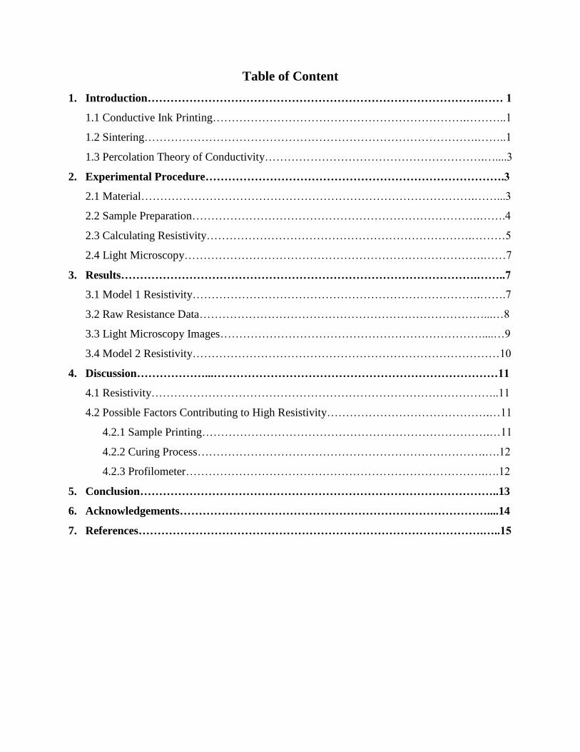
Table of Content
1. Introduction…………………………………………………………………………….…… 1
1.1 Conductive Ink Printing………………………………………………………….………..1
1.2 Sintering…………………………………………………………………………….……..1
1.3 Percolation Theory of Conductivity………………………………………………….…....3
2. Experimental Procedure…………………………………………………………………….3
2.1 Material…………………………………………………………………………….……...3
2.2 Sample Preparation………………………………………………………………….…….4
2.3 Calculating Resistivity…………………………………………………………….………5
2.4 Light Microscopy…………………………………………………………………….……7
3. Results………………………………………………………………………………….……..7
3.1 Model 1 Resistivity………………………………………………………………….…….7
3.2 Raw Resistance Data…………………………………………………………………...…8
3.3 Light Microscopy Images……………………………………………………………....…9
3.4 Model 2 Resistivity………………………………………………………………………10
4. Discussion………………...…………………………………………………………………11
4.1 Resistivity………………………………………………………………………………..11
4.2 Possible Factors Contributing to High Resistivity…………………………………….…11
4.2.1 Sample Printing………………………………………………………………….…11
4.2.2 Curing Process………………………………………………………………….….12
4.2.3 Profilometer…………………………………………………………………….….12
5. Conclusion…………………………………………………………………………………..13
6. Acknowledgements………………………………………………………………………....14
7. References……………………………………………………………………………….…..15
1
1. Introduction
1.1 Conductive Ink Printing
Printed electronics is a technology that has been improving throughout this decade. This
technology is used to create electrical devices on different substrates, such as making thin film
transistors, capacitors, resistors, batteries, circuits, etc. There are many different methods of
printing electronics, including screen printing, lithography, rotogravure, and screen printing.
Although these methods are already low cost processes by electronic industry standard, a newer
alternative, inkjet printing, can be even cheaper, more convenient, ease of mass production,
sustainable, and grants flexibility.2
One of the most used methods in electronics printing is lithography. It is widely adopted in the
circuit board industry for manufacturing circuits. This method involves many steps including
etching, electroplating, etc. It can be extremely time consuming, and somewhat expensive. The
etching agent used in lithography is also corrosive, and the choice of substrate is limited.
Because of these downfalls, the electronics industry is seeking improvements from inkjet
printing3,4,5.
Inkjet printing requires low viscosity liquid-phase materials to be printed through a nozzle. The
printed conductive ink will form a conductive line after drying. Inkjet printing’s ability to deliver
precise, small amount of ink in a quick fashion will make printing conductive ink easy, fast, and
effective. Ideally, the printed ink will dry quickly after printed due to the inkjet’s ability to keep
the amount of ink small and precise. The conductive inks used for printing are typically made of
copper and/or silver nanoparticles due to their high electrical conductivity in some kind of
organic solvent and polymer coating3,4,5.
1.2 Sintering
In order to reduce the ink into its corresponding metals, a sintering step is needed. Sintering is
the material atomic diffusion process driven by the reduction in the interfacial energy between
the metal particles. There are four possible diffusion paths during the sintering between two
particles (Figure 1). Paths 1 and 2 do not cause densification while paths 3 and 4 do.
Densification only occurs when the distance between the centers of the particles change6.
2
Figure 1. Possible diffusion paths between two metal particles during sintering6.
The sintering process can be low temperature due to the high surface to volume ratio of the nano-
particles. There are two different sintering technique available. The conventional radiation-
conduction- convection heating is the most commonly used method. The sintering temperatures
for this process are usually above 200 degrees Celsius, making a selective number of substrates
unusable such as thermoplastic polymers and paper. The other technique used is a laser sintering
method. The laser follows and sinters the printed tracks, not affecting the substrate. It is much
more effective compared to the previous technique. However, the laser method is usually very
costly4,6.
Without curing the printed ink trace and sintering the metal particles, nano-silver conductive ink
act as an insulator in its as dried state6. The nano-silver particles are coated in a stabilizing
polymer coating and submerged in a solvent designed to help initiate sintering at lower
temperatures (Figure 2). At elevated temperature, the solvent would evaporate and the polymer
coating would melt and flow away from the interparticle regions, forming an adhesive layer in
between the ink and the substrate. This allows the metal particles to come in contact and sinter.
Sintering not only render the printed ink tracks conductive, it also affects the physical and
electrical properties of the metal nanoparticle tracks. One major property that is linked to
sintering is resistivity. With lower sintering temperatures, the resistivity of printed metal
nanoparticle tracks can be up to 2 to 3 times lower than its theoretical bulk resistivity.

3
Figure 2. The movement of the nano-silver particles and the polymer coating at elevated temperatures during
curing.7
1.3 Percolation Theory of Conductivity
The percolation theory of conductivity describes the statistical behavior of electrical conductivity
in the clustered nano-silver particle system of the ink. When electricity travels through this
cluster of nano-silver particle structure, the electricity has a probability to percolate from one
particle to the next. This probability is depended on the density of the sintering of silver particles
in the structure, where the probability of percolation is extremely low until a specific percentage
is met. This percentage is called the percolation threshold. The percolation threshold can be
determined experimentally for different systems. In order to obtain good conductivity in the ink
traces, high degree of sintering is essential8,9.
2. Experimental Procedure
2.1 Material
The ink used in this project was the Metalon JS-B25P nano-silver ink purchased from
Novacentrix. The average silver particle size in this ink is 75 nm in diameter. The particles are
coated with ethylene glycol and submerged in polyethylene glycol 4 (tert- octylphenyl) ether.
The inkjet printer used in this project was an Epson C88+ Stylus photo printer purchased from
Novacentrix. The substrate used in this project was the Novele printing media purchased from
Novacentrix. The Novele printing media is a PET-based, transparent, mesoporous printing media
made for conductive ink inkjet printing.

4
2.2 Sample Preparation
Sample traces were printed on 3.5 inches by 5 inches sheets of Novele PET film with three traces
on each sheet as shown in Figure 3. After printing the sample traces, the samples were
transferred to a hotplate to be cured. The curing conditions selected for this project were 100,
120, 140, and 160 for 30 minutes, 60 minutes, 90 minutes, and 120 minutes. With each
sheet of three traces for each pair of temperature and time curing condition, a total of 16 PET
sheets of samples were prepared (Figure 4). The resistances of each of the sample traces was
measured after curing and recorded using a multimeter.
Figure 3. Diagram of the printed samples with three traces on each PET film.

5
Figure 4. 16 printed sample films with each sheet for one set of curing conditions.
2.3 Calculating Resistivity
The resistivity of the sample traces were calculated using equation 110, where ρ is resistivity, R is
resistance obtained from the multimeter, L is the length of the sample trace from end to end, and
A is the cross-sectional area of the ink.
(1)

6
Two different models were used to calculate the cross-sectional area of the ink trace. The first
model used is shown in Figure 5, where the cross-sectional areas of the ink traces were assumed
to be perfectly rectangular. With this model, the cross-sectional areas of each of the sample
traces were calculated by multiplying the width of the traces by the thickness of the traces
obtained using an AMBIOS Technology (XP-1) profilometer provided by the Cal Poly clean
room. The profilometer measures the thicknesses of the ink films by dragging a needle across the
surface of the samples and recording the vertical displacements of the needle tip, generating an
array of data points. Due to the rectangular cross-section assumption of the first model, the
thickness value was obtained by averaging the data point values from where the ink trace begins
and ends on the profilometer graph (Figure 6).
Figure 5. The assumed cross-section of the printed ink traces.
Figure 6. Example of a profilometer graph generated. For the first model, the thicknesses for the ink traces were
calculated by averaging the data points from where the ink trace begins and ends, represented by the two red lines.

7
The second model used to calculate the cross-sectional area of the ink traces is more precise than
the first model. In this model, the exact cross-sectional area of each sample trace was obtained
using the profilometer data by calculating the area under the curve as shown in Figure 7.
Figure 7. The second model used to calculate the cross-sectional area of the ink traces.
2.4 Light Microscopy
Light microscopy images were taken at 50x and 500x magnification using an Olympus BH2
UMA microscope provided by the Cal Poly Materials Engineering Department to observe the
surface pattern of the ink traces.
3. Results
3.1 Model 1 Resistivity
Resistivity values calculated using the rectangular cross-sectional area model were plotted
against the curing time for each of the curing temperature groups (Figure 8). As shown in the
graph, none of the curing conditions met the desired resistivity of 9.05x10⁻⁸ Ωm, which is five
times the resistivity of bulk silver, represented by the red dotted line. To see if there are any
significant statistical differences between the different sample groups, a 5% significance
ANOVA test was performed. The ANOVA test yielded a P-value of 0.406, which is greater than

8
0.05, demonstrating that there is no significant statistical difference between the resistivity values
of these curing conditions.
Figure 8. Resistivity from model 1 vs curing time.
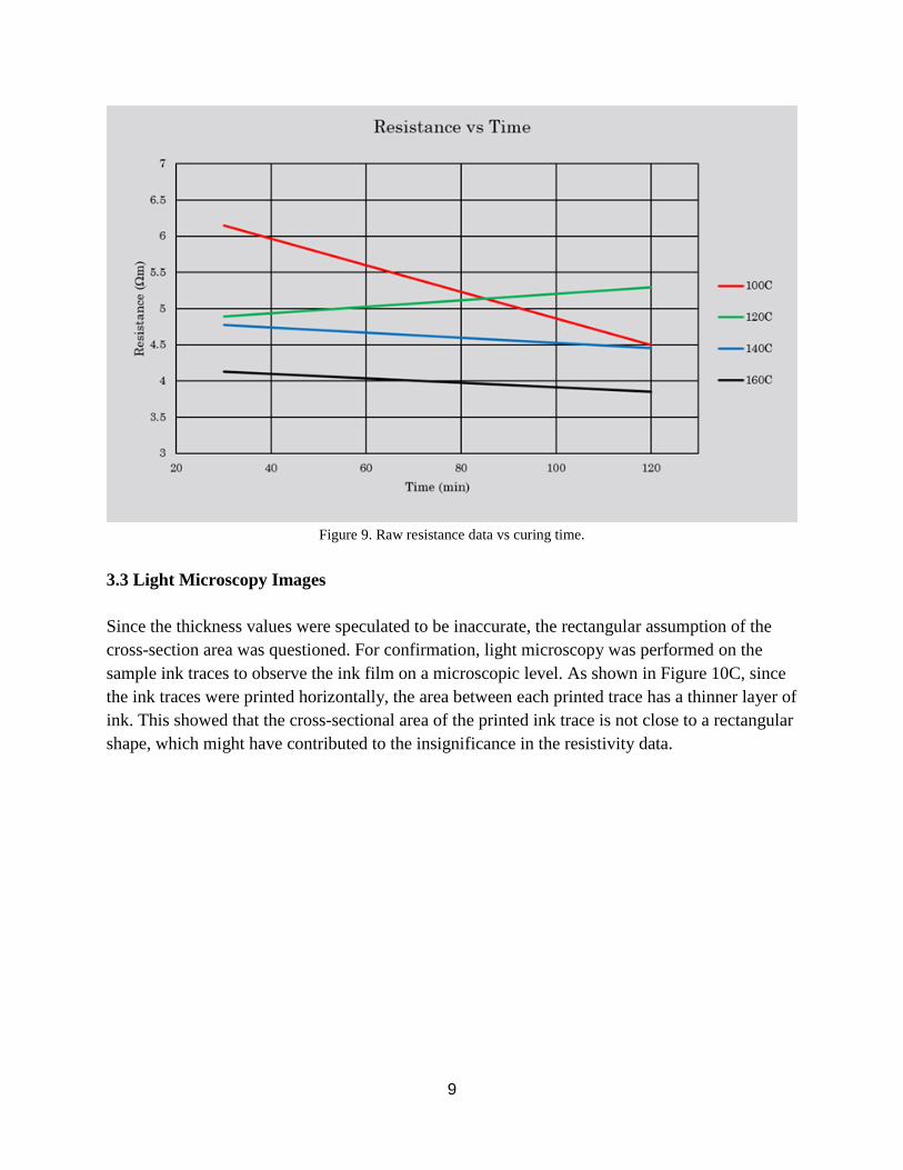
3.2 Raw Resistance Data
Due to the lack of statistical difference in model 1 resistivity results, the raw resistance data were
plotted against the curing times for each of the curing temperature groups (Figure 9). A 5%
ANOVA test was performed, and it yielded a P-value of 0.012, which is less than 0.05, meaning
that there are significant statistical differences between the temperature groups. By conducting a
Tukey pairwise comparison test, differences were found to reside between the 100 and the
160 groups, and between the 120 and the 160 groups. Since the raw resistance data
showed significant differences between some of the groups while the model 1 resistivity data did
not, the thickness values used to calculate resistivity were speculated to be the source of the
problem.
9
Figure 9. Raw resistance data vs curing time.
3.3 Light Microscopy Images
Since the thickness values were speculated to be inaccurate, the rectangular assumption of the
cross-section area was questioned. For confirmation, light microscopy was performed on the
sample ink traces to observe the ink film on a microscopic level. As shown in Figure 10C, since
the ink traces were printed horizontally, the area between each printed trace has a thinner layer of
ink. This showed that the cross-sectional area of the printed ink trace is not close to a rectangular
shape, which might have contributed to the insignificance in the resistivity data.

10
Figure 10. Light microscopy of 2 different sample traces cured at 140 for 30 minutes: first sample at (A) 50x and
(B) 500x, second sample at (C) 50x and (D) 500x.
3.4 Model 2 Resistivity
Resistivity values were calculated using the exact cross-sectional area model and were again
plotted against the curing time for all the curing temperature groups (Figure 11). As shown in the
graph, none of the curing conditions met the desired resistivity of 9.05x10⁻⁸ Ωm, and with a 5%
ANOVA test, the data yielded a P-value of 0.0983, showing no significant differences between
the data groups.
A C
B D

11
Figure 11. Model 2 Resistivity vs curing time graph.
4. Discussion
4.1 Resistivity
Both model 1 and 2 resistivity data did not meet the desired resistivity, and no significant
differences were found between the data sets for both the models. Although the raw resistance
data did show differences between some of the groups, those differences were not shown in the
resistivity data. Overall, the resistivity of the sample ink traces ranged from 1.4x10⁻⁷ Ωm to
3.5x10⁻⁷ Ωm. There are many factors that could have contributed to the yielding of the high
resistivity values on the sample ink traces.
4.2 Possible Factors Contributing to High Resistivity
4.2.1 Sample Printing
Light microscopy results showed inconsistencies in the printing of the sample traces. Many gaps,
holes, and other defects can be observed on the surface of the sample traces. For example, as
shown in Figure 10C and Figure 10D, large, through sample gaps were found on that specific
sample ink trace. Since the resistance values were measured using one point on each end of the
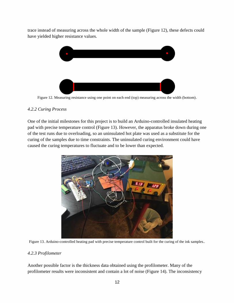
12
trace instead of measuring across the whole width of the sample (Figure 12), these defects could
have yielded higher resistance values.
Figure 12. Measuring resistance using one point on each end (top) measuring across the width (bottom).
4.2.2 Curing Process
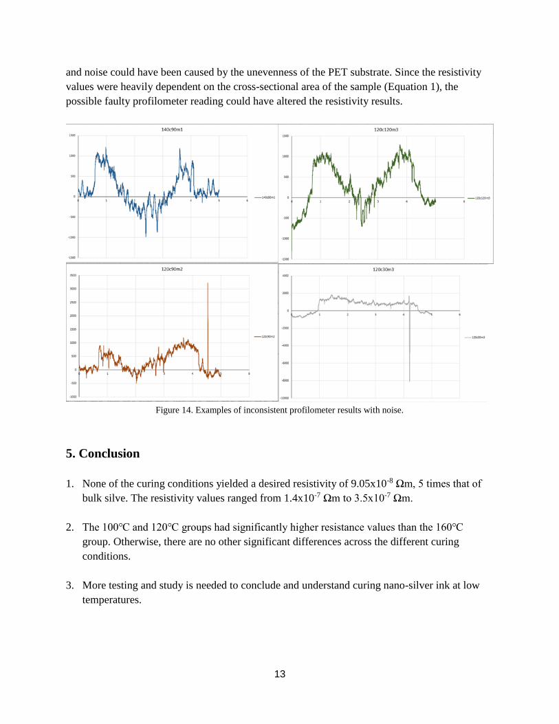
One of the initial milestones for this project is to build an Arduino-controlled insulated heating
pad with precise temperature control (Figure 13). However, the apparatus broke down during one
of the test runs due to overloading, so an uninsulated hot plate was used as a substitute for the
curing of the samples due to time constraints. The uninsulated curing environment could have
caused the curing temperatures to fluctuate and to be lower than expected.
Figure 13. Arduino-controlled heating pad with precise temperature control built for the curing of the ink samples..
4.2.3 Profilometer
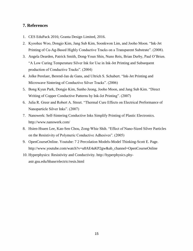
Another possible factor is the thickness data obtained using the profilometer. Many of the
profilometer results were inconsistent and contain a lot of noise (Figure 14). The inconsistency
13
and noise could have been caused by the unevenness of the PET substrate. Since the resistivity
values were heavily dependent on the cross-sectional area of the sample (Equation 1), the
possible faulty profilometer reading could have altered the resistivity results.
Figure 14. Examples of inconsistent profilometer results with noise.
5. Conclusion
1. None of the curing conditions yielded a desired resistivity of 9.05x10⁻⁸ Ωm, 5 times that of
bulk silve. The resistivity values ranged from 1.4x10⁻⁷ Ωm to 3.5x10⁻⁷ Ωm.
2. The 100 and 120 groups had significantly higher resistance values than the 160
group. Otherwise, there are no other significant differences across the different curing
conditions.
3. More testing and study is needed to conclude and understand curing nano-silver ink at low
temperatures.

14
6. Acknowledgments
I would like to thank to Dr. Linda Vanasupa for advising and guiding me throughout this project.
15
7. References
1. CES EduPack 2016; Granta Design Limited, 2016.
2. Kyoohee Woo, Dongjo Kim, Jang Sub Kim, Soonkwon Lim, and Jooho Moon. “Ink-Jet
Printing of Cu-Ag-Based Highly Conductive Tracks on a Transparent Substrate”. (2008).
3. Angela Dearden, Patrick Smith, Dong-Youn Shin, Nuno Reis, Brian Derby, Paul O’Brien.
“A Low Curing Temperature Silver Ink for Use in Ink-Jet Printing and Subsequent
production of Conductive Tracks”. (2004)
4. Jolke Perelaer, Berend-Jan de Gans, and Ultrich S. Schubert. “Ink-Jet Printing and
Microwave Sintering of Conductive Silver Tracks”. (2006)
5. Bong Kyun Park, Dongjo Kim, Sunho Jeong, Jooho Moon, and Jang Sub Kim. “Direct
Writing of Copper Conductive Patterns by Ink-Jet Printing”. (2007)
6. Julia R. Greer and Robert A. Street. “Thermal Cure Effects on Electrical Performance of
Nanoparticle Silver Inks”. (2007)
7. Nanowerk: Self-Sintering Conductive Inks Simplify Printing of Plastic Electronics.
http://www.nanowerk.com/
8. Hsien-Hsuen Lee, Kan-Sen Chou, Zong-Whie Shih. “Effect of Nano-Sized Silver Particles
on the Resistivity of Polymeric Conductive Adhesives”. (2005)
9. OpenCourseOnline. Youtube: 7 2 Percolation Models-Model Thinking-Scott E. Page.
http://www.youtube.com/watch?v=u8AE4aKP2gw&ab_channel=OpenCourseOnline
10. Hyperphysics: Resistivity and Conductivity. http://hyperphysics.phy-
astr.gsu.edu/hbase/electric/resis.html