presentation on fundamentals of mixer design - agilent technologies
TRANSCRIPT

This document is owned by Agilent Technologies, but is no longer kept current and may contain obsolete or
inaccurate references. We regret any inconvenience this may cause. For the latest information on Agilent’s
line of EEsof electronic design automation (EDA) products and services, please go to:
www.agilent.com/fi nd/eesof
Agilent EEsof EDA

1
H•4/17/01
DDesignesignSSeminareminar
Agilent EEsof Agilent EEsof Customer EducationCustomer Educationand Applicationsand Applications
Fundamentals of Mixer Design
Abstract
The mixer is used in nearly all RF/Microwave systems for frequency translation. This seminar explains how mixers provide this function and why they often generate so many spurious outputs as well. Issues such as single vs. double balanced, active vs. passive, nonlinear vs. switching mode mixers will be discussed. Mixer performance measures such as image rejection, conversion gain, gain compression, intercept and intermodulation, noise figure, dynamic range, and isolation will be explained.

2
H•4/17/01
Page 2
About the Author
Steve Long
• University of California, Santa Barbara • Professor, Electrical and Computer Engineering • Consultant to Industry
BIOGRAPHICAL SKETCH
Stephen Long received his BS degree in Engineering Physics from UC Berkeley and MS and PhD in Electrical Engineering from Cornell University. He has been a professor of electrical and computer engineering at UC Santa Barbara since 1981. The central theme of his current research projects is rather practical: use unconventional digital and analog circuits, high performance devices and fabrication technologies to address significant problems in high speed electronics such as low power IC interconnections, very high speed digital ICs, and microwave analog integrated circuits for RF communications. He teaches classes on communication electronics and high speed digital IC design.
Prior to joining UCSB, from 1974 to 1977 he was a Senior Engineer at Varian Associates, Palo Alto, CA. From 1978 to 1981 he was employed by Rockwell International Science Center, Thousand Oaks, CA as a member of the technical staff.
Dr. Long received the IEEE Microwave Applications Award in 1978 for development of InP millimeter wave devices. In 1988 he was a research visitor at GEC Hirst Research Centre, U.K. In 1994 he was a Fulbright research visitor at the Signal Processing Laboratory, Tampere University of Technology, Finland and a visiting professor at the Electromagnetics Institute, Technical University of Denmark. He is a senior member of the IEEE and a member of the American Scientific Affiliation.

3
H•4/17/01
Page 3
Basic engineering problem:
• Understand operating principles of the mixer
• What makes a good mixer?
• Choices: Nonlinear/switching mode; single/double balance; active/passive
• Specify performance: Gain, NF, P1dB, TOI, SFDR, isolation, image rejection
• Review some mixer design examples
Choosing the right mixer for the task...
Learning Objectives:
Always see the NOTES pages for Exercises throughout...
There are many different mixer circuit topologies and implementations that are suitable for use in receiver and transmitter systems. How do you select the best one for a particular application? Why does the choice depend on the application and technology available?

4
H•4/17/01
Page 4
Why study mixers?
• Receivers
• up or down conversion
• demodulation of SC SSB or SC DSB
• input must support large dynamic range
• AGC
• Transmitters
• up conversion
• modulation: amplitude and phase
• input has optimum signal level for high performance
Mixers have a wide variety of applications in communication systems.
The superheterodyne receiver architecture often has several frequency translation stages (IF frequencies) to optimize image rejection, selectivity, and dynamic range. Direct conversion receiver architectures such as used in pagers use mixers at the input to both downconvert and demodulate the digital information. Mixers are thus widely used in the analog/RF front end of receivers. In these applications, often the mixer must be designed to handle a very wide dynamic range of signal powers at the input.
The mixer can be used for demodulation, although the trend is to digitize following a low IF frequency and implement the demodulation function digitally. They can also be used as analog multipliers to provide gain control. In this application, one input is a DC or slowly varying RSSI signal which when multiplied by the RF/IF signal will control the degree of gain or attenuation.
In transmitter applications, the mixer is often used for upconversion or modulation. In this application, the input signal level can be selected to optimize the overall signal-to-noise ratio at the output.

5
H•4/17/01
Page 5
What is a mixer?
• Frequency translation device
• Ideal mixer:
• Doesn’t “mix”; it multiplies
A
B
AB
[ ]ttAB
tBtA )cos()cos(2
)sin)(sin( 212121 ωωωωωω +−−=Downconvert Upconvert
ω1 − ω2 ω1 + ω2
ω1 and ω2
suppressed No harmonics
A mixer doesn’t really “mix” or sum signals; it multiplies them.
Note that both sum and difference frequencies are obtained by the multiplication of the two input sinusoidal signals. A mixer can be used to either downconvert or upconvert the RF input signal, A. The designer must provide a way to remove the undesired output, usually by filtering.
[ ]ttABtBtA )cos()cos(2
)sin)(sin( 212121 ωωωωωω +−−=

6
H•4/17/01
Page 6
Images
• Two inputs (RF & Image) will mix to the same output (IF) frequency.
• The image frequency must be removed by filtering
• fIF and fLO must be carefully selected
• Image rejection ratio: dB(PIF desired/PIF image)
fIF fRFfLOfIM
fIF fIF
fLO+fIM fLO+fRF
INPUTSSUM OUTPUTS
DIFFERENCEOUTPUTS
Even in an ideal multiplier, there are two RF input frequencies (FRF and FIM) whose second-order product has the same difference IF frequency.
FRF - FLO = FLO - FIM = FIF
The two results are equally valid. One is generally referred to as the “image” and is undesired. In the example above, the lower input frequency is designated the image.

7
H•4/17/01
Page 7
Image rejection preselector
fIF fRFfLOfIM
fIF fIF
fLO+fIM fLO+fRF
INPUTSSUM OUTPUTS
DIFFERENCEOUTPUTS
IFRF
LO
BPF
A bandpass preselection filter is often used ahead of the mixer to suppress the image signal. The IF and LO frequencies must be carefully selected to avoid image frequencies that are too close to the desired RF frequency to be effectively filtered.
In a receiver front end, out-of-band inputs at the image frequency could cause interference when mixed to the same IF frequency. Also, the noise present at the image would also be translated to the IF band, degrading signal-to-noise ratio.
Alternatively, an image-rejection mixer could be designed which suppresses one of the input sidebands by phase and amplitude cancellation. This approach requires two mixers and some phase-shifting networks.
So far, the spectrum exhibited by the ideal multiplier is free of harmonics and other spurious outputs (spurs). The RF and LO inputs do not show up in the output. While accurate analog multiplier circuits can be designed, they do not provide high dynamic range mixers since noise and bandwidth often are sacrificed for accuracy.

8
H•4/17/01
Page 8
Mixer operating mechanisms
• Nonlinear transfer function
• use device nonlinearities creatively!
• useful at mm-wave frequencies
• Switching or sampling
• a time-varying process
• preferred; fewer spurs
High performance RF mixers use nonlinear characteristics to generate the multiplication. Thus, they also generate lots of undesired output frequencies.
Three techniques have proven to be effective in the implementation of mixers with high dynamic range:
1. Use a device that has a known and controlled nonlinearity.
2. Switch the RF signal path on and off at the LO frequency.
3. Sample the RF signal with a sample-hold function at the LO frequency.
The nonlinear mixer can be applicable at any frequency where the device presents a known nonlinearity. It is the only approach available at the upper mm-wave frequencies. When frequencies are low enough that good switches can be built, the switching mixer mode is preferred because it generates fewer spurs. In some cases, sampling has been substituted for switching.

9
H•4/17/01
Page 9
Nonlinear mixer operation
Any diode or transistor will exhibit nonlinearityin its transfer characteristic at sufficiently high signal levels.
VRF(t)
+ VO(t) −
RL
RS
VLO(t)
Λ++++= )()()()( 33
2210 tvatvatvaatV inininO
vin(t) second-order product term
We see that our output may contain a DC term, RF and LO feedthrough, and terms at all harmonics of the RF and LO frequencies. Only the second-order product term produces the desired output.
In addition, when vRF consists of multiple carriers, the power series also will produce cross-products that make the desired output products dependent on the amplitude of other inputs.
Spurious output signal strengths can be decreased when devices that are primarily square-law, such as FETs with longer gate lengths, are used in place of diodes or bipolar transistors.

10
H•4/17/01
Page 10
Unbalanced diode mixer output
FRF = 110 MHz |VRF| = 0.1VFLO = 100 MHz |VLO| = 0.2V VDC = 0.6V
We can see that there are a lot of spurious outputs generated. Ideally, we would like to see outputs only at 10 MHz and 210 MHz. So, we prefer the switching type mixer when the RF and LO frequencies are low enough that we can make decent switches. This takes us up through much of the mm-wave spectrum.
[See ADS example file diode1.dsn]
11
H•4/17/01
Page 11
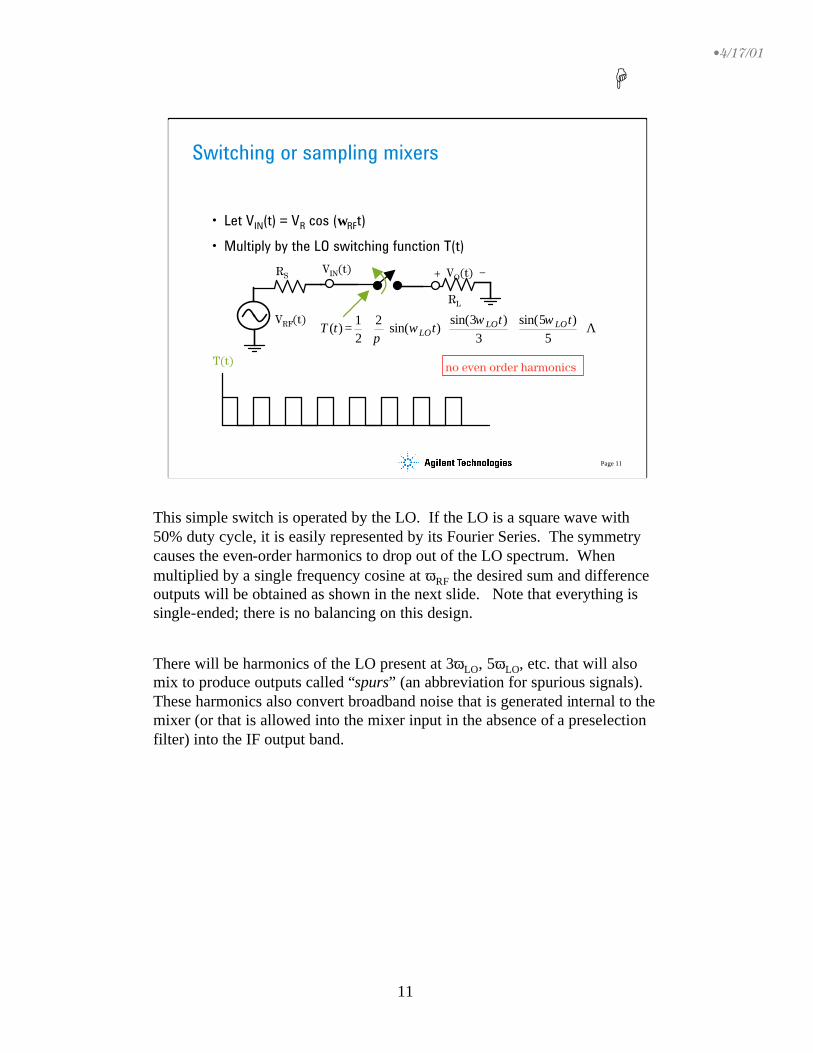
Switching or sampling mixers
• Let VIN(t) = VR cos (ωRFt)
• Multiply by the LO switching function T(t)
VRF(t)
T(t)
++++= Λ
5)5sin(
3)3sin(
)sin(221)(
ttttT LOLO
LOωω
ωπ
RL
RS
no even order harmonics
+ VO(t) −VIN(t)
This simple switch is operated by the LO. If the LO is a square wave with 50% duty cycle, it is easily represented by its Fourier Series. The symmetry causes the even-order harmonics to drop out of the LO spectrum. When multiplied by a single frequency cosine at ωRF the desired sum and difference outputs will be obtained as shown in the next slide. Note that everything is single-ended; there is no balancing on this design.
There will be harmonics of the LO present at 3ωLO, 5ωLO, etc. that will also mix to produce outputs called “spurs” (an abbreviation for spurious signals). These harmonics also convert broadband noise that is generated internal to the mixer (or that is allowed into the mixer input in the absence of a preselectionfilter) into the IF output band.

12
H•4/17/01
Page 12
Mixer output
+++= Λ
3)3sin()cos(
)sin()cos(2
)cos(2
)(tt
ttV
tV
tV LORFLORF
RRF
Ro
ωωωω
πω
RF feedthrough 2nd-order product 4th-order spurs
LO 3LORF RF+LORF−LO 3LO−RF 3LO+RF
VO(ω)
ω
The product of VRF(t)T(t) produces the desired output frequencies at
ωRF − ωLO and ωRF + ωLO from the second order product.
Odd harmonics of the LO frequency are also present since we have a square wave LO switching signal. These produce spurious 4th, 6th, … order products with outputs at
nωLO − ωRF and nωLO + ωRF where n is odd.
We also get RF feedthrough directly to the output.
None of the LO signal should appear in the output if the mixer behaves according to this equation. But, if there is a DC offset on the RF input, there will be a LO frequency component in the output as well. This requirement is not unusual, since many mixer implementations require some bias current which leads to a DC offset on the input.
EXERCISE 1: Use the diode in the nonlinear diode mixer simulation as a switch. Put a square wave LO in series with the RF generator and simulate the output spectrum using transient analysis. (solution in ADS file ex1)
[See ADS example files swmix2.dsn and diode1.dsn]

13
H•4/17/01
Page 13
Isolation between ports
• The mixer is not perfectly unilateral -
leakage between:
• LO to IF
• LO to RF
• RF to IF
• Determine the magnitude of these leakage components at the IF and RF ports using harmonic balance.
• Use the mix function to select frequencies.
Isolation can be quite important for certain mixer applications. For example, LO to RF leakage can be quite serious in direct conversion receiver architectures because it will remix with the RF and produce a DC offset. Large LO to IF leakage can degrade the performance of a mixer postamp if it is located prior to IF filtering.
EXERCISE 2: Modify the data display swmix2.dds to measure the LO to IF, LO to RF, and RF to IF isolation. Express these isolations as power ratios.
(solution in ADS display file ex2.dds)

14
H•4/17/01
Page 14
Conversion gain or loss
==
S
RF
L
IF
IF
Rv
Rv
powerinputavailableRFFatpowerOutput
ConvGain
8
22
2
• Generally expressed as a voltage gain or as a transducer power gain
VRF VLO(t)
RS
RL+VIF−
+VIN−
IN
IFV V
VA =
Conversion gain is usually defined as the ratio of the IF output power to the available RF source power. So we can be compatible with ADS output format, in these equations, the voltages are peak amplitudes, not RMS. If the source and load impedances are different, the power gain must account for this as shown. Voltage gains are also useful, especially in RFIC implementations of mixers.
Active or passive implementations can be used for the mixer. Each has its advantages and disadvantages. The passive implementations using diodes as nonlinear elements or switches or FETs as passive switches always exhibit conversion loss rather than gain. This can impact the overall system noise performance, so if noise is critical, an LNA is usually added before the mixer.
We see that the simple switching mixer has low conversion gain because the voltage gain AV is only 1/π. Also, the RF feedthrough problem and in most instances, an LO feedthrough problem exist. All of these deficiencies can be improved by the use of balanced topologies which provide some cancellation of RF and LO signals as well as increasing conversion gain.
15
H•4/17/01
Page 15
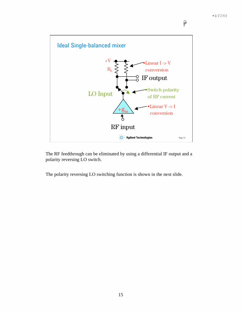
Ideal Single-balanced mixer
+gm
LO Input
+V
IF output
•Switch polarityof RF current
•Linear V -> Iconversion
•Linear I -> VconversionRL
RF input
The RF feedthrough can be eliminated by using a differential IF output and a polarity reversing LO switch.
The polarity reversing LO switching function is shown in the next slide.

16
H•4/17/01
Page 16
LO Switching Function T(t)
+++−=
+++=
....)3sin(31
)sin(2
21
)(
....)3sin(31
)sin(2
21
)(
2
1
tttT
tttT
LOLO
LOLO
ωωπ
ωωπ
T1(t)
T2(t)
T(t) = T1(t) + T2(t)
SUM OF SWITCHING FUNCTIONS
When added together, the DC terms (1/2 & -1/2) cancel. The DC term was responsible for the RF feedthrough in the unbalanced mixer since the cos(ωRFt) term was multiplied only by T1(t).
Second-order term:
Here we see that the ideal conversion gain (VIF/VR)2 = A2 (2/π)2
(if A=1) is 6 dB greater than for the unbalanced design.
But, we can still get LO feedthrough if there is a DC current in the signal path. This is often the case since the output of the transconductance amplifier will have a DC current component. This current shows up as a differential output.
[ ]...)5sin()3sin()sin()cos()( 51
314
+++= ttttAVtV LOLOLORFRIF ωωωω π
[ ]ttAV
LORFLORFR )sin()sin(
2ωωωω
π−−+

17
H•4/17/01
Page 17
Output spectrum: SB mixer
FRF = 200 MHzFLO = 1.0 GHzFIF @ 800 & 1200 MHz
LO feedthrough
FIF FIF
3FLO
3FLO - FRF
5FLO
VIF = V1 − V2
DC offset
RF input
LO
As you can see, the output spectrum of the single-balanced switching mixer is much less cluttered than the nonlinear mixer spectrum. This was simulated with transient analysis using an ideal switch. The behavioral switch model has an on-threshold of 2V and an off-threshold of 1V. The LO was generated with a 4V pulse function and the duty cycle was set to 50%. The output is taken differentially as VIF = V1 - V2.
Note the strong LO feedthrough component in the output. This is present because of the DC offset on the RF input which produces a differential LO voltage component in the output.
[See ADS example file swmixer1.dsn]
EXERCISE 3: Set the DC offset voltage to 0 and resimulate. Observe that the LO feedthrough is gone. Compare V1 and VIF vs time with and without the DC offset. Use markers to measure the IF output power and calculate the conversion gain. (solution in ADS file ex3)
This LO component is highly undesirable because it could desensitize a mixer postamplifier stage if the amplification occurs before IF filtering. Eliminating the LO component when a DC current is present requires double-balancing.

18
H•4/17/01
Page 18
Ideal Double Balanced Mixer
-gm +gm
RF input
LO Input
+V
IF output
•Switch polarityof RF current
•Linear V -> Iconversion
•Linear I -> VconversionRL RL
An ideal double balanced mixer consists of a switch driven by the local oscillator that reverses the polarity of the RF input at the LO frequency[1] and a differential transconductance amplifier stage. The polarity reversing switch and differential IF cancels any output at the RF input frequency since the DC term cancels as was the case for the single balanced design. The double LO switch cancels out any LO frequency component, even with currents in the RF to IF path, since we are taking the IF output as a differential signal and the LO shows up now as common mode. Therefore, to take full advantage of this design, an IF balun, either active (a differential amplifier) or passive (a transformer or hybrid), is required. The LO is typically suppressed by 50 or 60 dB if the components are well matched and balanced.
To get the highest performance from the mixer we must make the RF to IF path as linear as possible and minimize the switching time of the LO switch. The ideal mixer above would not be troubled by noise (at the low end of the dynamic range) or intermodulation distortion (IMD) at the high end since the transconductors and resistors are linear and the switches are ideal.

19
H•4/17/01
Page 19
Output Spectrum: DB mixer
FRF = 200 MHzFLO = 1.0 GHzFIF @ 800 & 1200 MHz
NO LO or RF feedthrough
Polarity reversing switch functionis easily seen here
Differential output voltage
The differential output voltage and frequency spectrum are simulated using a transient analysis in ADS. The polarity switching action can be clearly seen in the output voltage. There is no LO or RF feedthrough in this ideal DB mixer, even with a DC current in the signal path.
[See ADS example file: swmixer3.dsn]
In real mixers, there is always some imbalance. Transistors and baluns are never perfectly matched or balanced. These nonidealities will produce some LO to IF or RF to IF feedthrough (thus, isolation is not perfect). This is usually specified in terms of a power ratio relative to the desired IF output power: dBc
Secondly, the RF to IF path is not perfectly linear. This will lead tointermodulation distortion. Odd-order distortion (typically third and fifth order are most significant) will cause spurs within the IF bandwidth or cross-modulation when strong signals are present. Also, the LO switches are not perfectly linear, especially while in the transition region. This can add more distortion to the IF output and will increase loss due to the resistance of the switches.

20
H•4/17/01
Page 20
Mixer Performance Specifications
• Image rejection
• Conversion gain: voltage or power
• Port-to-port isolation: dBc
• Large signal performance:
• gain compression: P1dB
• intermodulation distortion spec: third-order intercept (TOI)
• Small signal performance: noise figure
• Operating range: Spurious-free dynamic range
We have already discussed image rejection, conversion gain and isolation. Other performance specifications relate to the mixer’s ability to work with very weak and very strong signals.
We would like to maximize mixer performance by:
1. maximize linearity in the signal path
2. idealize switching: high slew rates
3. minimize noise contributions
21
H•4/17/01
Page 21
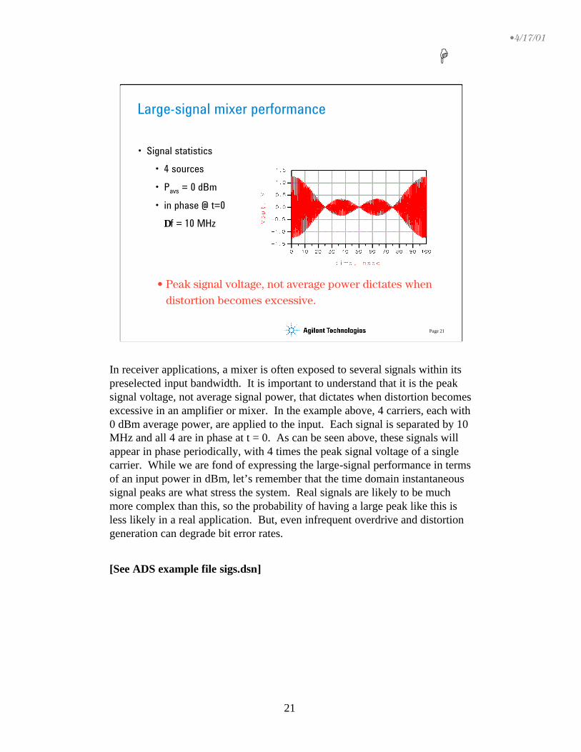
Large-signal mixer performance
• Signal statistics
• 4 sources
• Pavs = 0 dBm
• in phase @ t=0
∆f = 10 MHz
• Peak signal voltage, not average power dictates whendistortion becomes excessive.
In receiver applications, a mixer is often exposed to several signals within its preselected input bandwidth. It is important to understand that it is the peak signal voltage, not average signal power, that dictates when distortion becomes excessive in an amplifier or mixer. In the example above, 4 carriers, each with 0 dBm average power, are applied to the input. Each signal is separated by 10 MHz and all 4 are in phase at t = 0. As can be seen above, these signals will appear in phase periodically, with 4 times the peak signal voltage of a single carrier. While we are fond of expressing the large-signal performance in terms of an input power in dBm, let’s remember that the time domain instantaneous signal peaks are what stress the system. Real signals are likely to be much more complex than this, so the probability of having a large peak like this is less likely in a real application. But, even infrequent overdrive and distortion generation can degrade bit error rates.
[See ADS example file sigs.dsn]

22
H•4/17/01
Page 22
Gain Compression
• Conversion gain degrades at large input signal levels due to nonlinearity in the signal path.
• Assume a simple nonlinear transfer function:3
3)( ininRF vavtV −=
)3sin(41
)sin(4
31)( 3
3
23 tVatVa
VtV RFRRFR
RRF ωω +
−=
Gain compression Third-order distortion
•This distortion then gets mixed to the IF frequency
Gain compression is a useful index of distortion generation. It is specified interms of an input power level (or peak voltage) at which the small signal conversion gain drops off by 1 dB.
The example above assumes that a simple cubic function represents the nonlinearity of the signal path. When we substitute vin(t) = VR sin (ωRFt) and use trig identities, we see a term that will produce gain compression:
1 - 3a3VR2/4.
If we knew the coefficient a3, we could predict the 1 dB compression input voltage. Typically, we obtain this by measurement of gain vs. input voltage. The reduced amplitude output voltage then gets mixed down to the IF frequency.
We also see a cubic term that represents the third-order harmonic distortion(HD) that also is caused by the nonlinearity of the signal path. Harmonic distortion is easily removed by filtering; it is the intermodulation distortionthat results from multiple signals that is more troublesome to deal with.
Note that in this simple example, the fundamental is proportional to VRwhereas the third-order HD is proportional to VR
3. Thus, if Pout vs. Pin were plotted on a dB scale, the HD power will increase at 3 times the rate that the fundamental power increases with input power. This is often referred to as being “well behaved”, although given the choice, we could easily live without this kind of behavior!

23
H•4/17/01
Page 23
Use Harmonic Balance simulation
•Highest order of IM products•Fundamental Frequencies:
put highest power source first•Number of harmonics of sources [1] & [2]•Sweep P_RF in 1 dB steps from −15 dBm•Can be used to pass variables to data display
Harmonic balance is the method of choice for simulation of mixers. By specifying the number of harmonics to be considered for the LO and RF input frequencies and the maximum order (highest order of sums and differences) to be retained, you get the frequency domain result of the mixer at all relevant frequencies. To get this information using SPICE or other time domain simulators can often require a very long simulation time since at least two complete periods of the lowest frequency component must be generated in order to get accurate FFT results. This becomes a serious problem with two-tone input simulations. Concurrently, the time step must be compatible with the highest frequency component to be considered.
Maximum order corresponds to the highest order mixing product (n + m) to be considered (nf[1] ± mf[2]). The simulation will run faster with lower order and fewer harmonics of the sources, but may be less accurate. You should test this by checking if the result changes significantly as you increase order or number of harmonics.
The frequency with the highest power level (the LO) is always the first frequency to be designated in the harmonic balance controller. Other inputs follow sequencing from highest to lowest power.

24
H•4/17/01
Page 24
Gain Compression: P1dB
P1dB
The RF mixer behavioral model in ADS has been used to illustrate the gain compression phenomenon. The input RF power (P_RF) was swept from -15dBm to +5 dBm. On the left, we see the simulated IF output power vs. the ideal output power. Ideal output power is calculated from the small signal conversion gain, simulated at the lowest P_RF input power level, P_RF[0].Here, the index [0] refers to the first entry in the data set for P_RF, -15 dBm. The dBm(VIF[0]) function is used to convert the corresponding first entry in the IF voltage data set IF to power.
VIF is the output voltage at the IF output frequency and must be selected from many frequencies in the output data set. This frequency is selected by using the mix function. In this example, LOfreq = 1 GHz and RFfreq = 0.85 GHz. If we are interested in the downconverted IF frequency, 150 MHz, we can select it from:
VIF = mix(Vout,1,-1).
The indices in the curly brackets are ordered according to the HB fundamental analysis frequencies. Thus, 1,-1 selects LOfreq − RFfreq.
Other equations are added to the display panel which calculate the conversion gain
ConvGain = dBm(VIF) − P_RF.
Here we can identify the 1 dB gain compression power to be about 0 dBm.
[Refer to ADS example RFmixer_GC]

25
H•4/17/01
Page 25
Intermodulation distortion
• IMD consists of the higher order signal products that are generated when two RF signals are present at the mixer input. The IMD will be down and up converted by the LO as will the desired RF signal.
• IMD generation is a good indicator of large signal performance of a mixer.
• Absolute accuracy is highly dependent on the accuracy of the device model, but the relative accuracy is valuable for optimizing the circuit parameters for best IMD performance.
The gain compression power characterization provides a good indication of the signal amplitude that the mixer will tolerate before really bad distortion is generated. You should stay well below the P1dB input level.
Another measure of large-signal capability is the intermodulation distortion. Intermodulation distortion occurs when two or more signals are present at the RF input to the mixer. The LO input is provided as before. These two signals can interact with the nonlinearities in the mixer signal path (RF to IF) to generate unwanted IMD products (distortion) which then get mixed down to IF.

26
H•4/17/01
Page 26
Intermodulation Distortion
• Let’s consider the 3rd order nonlinearity: a3vin3
• two inputs: vin = V1 sin(ω1t) + V2 sin(ω2t)
])(sin)sin(3)sin()(sin3
)(sin)(sin[
22
12
21212
22
1
233
2133
133
ttVVttVV
tVtVaVout
ωωωω
ωω
+
++=
[ ] tttaVV
)2sin()2sin()sin(2
321212
12
322
1 ωωωωω +−−−
Cross-modulation Third-order IMD
Let’s consider again the simple cubic nonlinearity a3vin3. When two inputs at
ω1 and ω2 are applied simultaneously to the RF input of the mixer, the cubing produces many terms, some at the harmonics and some at the IMD frequency pairs. The trig identities show us the origin of these nonidealities. [4]
We will be mainly concerned with the third-order IMD. This is especially troublesome since it can occur at frequencies within the IF bandwidth. For example, suppose we have 2 input frequencies at 899.990 and 900.010 MHz. Third order products at 2f1 - f2 and 2f2 - f1 will be generated at 899.980 and 900.020 MHz. Once multiplied with the LO frequency, these IMD products may fall within the filter bandwidth of the IF filter and thus cause interference to a desired signal. IMD power, just as HD power, will have a slope of 3 on a dB plot.
In addition, the cross-modulation effect can also be seen. The amplitude of one signal (say ω1) influences the amplitude of the desired signal at ω2through the coefficient 3V1
2V2a3/2. A slowly varying modulation envelope on V1 will cause the envelope of the desired signal output at ω2 to vary as well since this fundamental term created by the cubic nonlinearity will add to the linear fundamental term. This cross-modulation can have annoying or error generating effects at the IF output.
Other higher odd-order IMD products, such as 5th and 7th, are also of interest, but may be less reliably predicted unless the device model is precise enough to give accurate nonlinearity in the transfer characteristics up to the 2n-1th order.

27
H•4/17/01
Page 27
IMD simulation
• Use a two-tone generator at themixer input.
• The two input frequencies are separated by Fspacing and each have an input power of P_RF dBm.
•Large MaxOrder and LO Order areneeded for accurate HB TOI predictionswith highly nonlinear elements•Oversampling (Param menu) shouldalso be increased cautiously
The IMD simulation is performed with a two-tone generator at the RF input. The frequency spacing should be small enough so that both fall within the IF bandwidth. You should keep in mind that both of the generator tones are in phase, therefore the peak voltage will add up periodically to twice the peak of each source independently. Because of this, you will expect to see some reduction in the P1dB on the order of 6 dB.
Often accurate IMD simulations will require a large maximum order and LO harmonic order when using harmonic balance. In this case, a larger number of spectral products will be summed to estimate the time domain waveform and therefore provide greater accuracy. This will increase the size of the data file and time required for the simulation. Increase the orders in steps of 2 and watch for changes in the IMD output power. When no further significant change is observed, then the order is large enough. Simulation of very low power levels is subject to convergence errors and numerical noise[6].
Sometimes, increasing the oversampling ratio for the FFT calculation (use the Param menu of the HB controller panel) can reduce errors. This oversamplingcontrols the number of time points taken when converting back from time to frequency domain in the harmonic balance simulation algorithm. A larger number of time samples increases the accuracy of the tranform calculation but increases memory requirements and simulation time. Both order and oversampling should be increased until you are convinced that further increases are not worthwhile.
28
H•4/17/01
Page 28
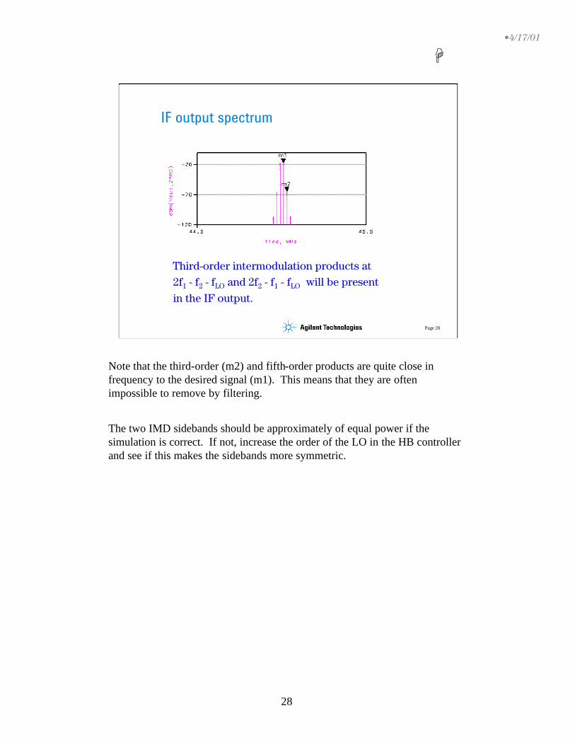
IF output spectrum
Third-order intermodulation products at 2f1 - f2 - fLO and 2f2 - f1 - fLO will be present in the IF output.
Note that the third-order (m2) and fifth-order products are quite close in frequency to the desired signal (m1). This means that they are often impossible to remove by filtering.
The two IMD sidebands should be approximately of equal power if the simulation is correct. If not, increase the order of the LO in the HB controller and see if this makes the sidebands more symmetric.

29
H•4/17/01
Page 29
Third-order intercept definition
IIP3
OIP3
slope = 3
slope = 1
A widely-used figure of merit for IMD is the third-order intercept (TOI) point. This is a fictitious signal level at which the fundamental and third-order product terms would intersect. In reality, the intercept power is 10 to 15 dBm higher than the P1dB gain compression power, so the circuit does not amplify or operate correctly at the IIP3 input level. The higher the TOI, the better the large signal capability of the mixer.
It is common practice to extrapolate or calculate the intercept point from data taken at least 10 dBm below P1dB. One should check the slopes to verify that the data obeys the expected slope = 1 or slope = 3 behavior. In this example, we can see that this is true only at lower signal power levels.
OIP3 = (PIF − PIMD)/2 + PIF.
Also, the input and output intercepts are simply related by the gain:
OIP3 = IIP3 + conversion gain.
In the data display above, equations are used to select out the IF fundamental tone and the IMD tone, in this case, the lower sideband. The mix function now has 3 indices since there are 3 frequencies present: LO, RF1 and RF2.
[See ADS example file: RFmixer_TOI]
30
H•4/17/01
Page 30
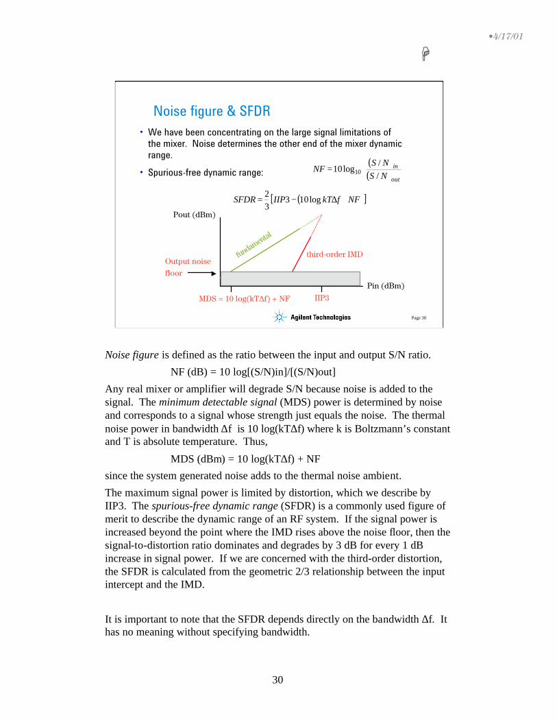
Noise figure & SFDR• We have been concentrating on the large signal limitations of
the mixer. Noise determines the other end of the mixer dynamic range.
• Spurious-free dynamic range:
Output noisefloor
Pout (dBm)
MDS = 10 log(kT∆f) + NF IIP3Pin (dBm)
fundamental
third-order IMD
( )[ ]NFfkTIIPSFDR +∆−= log10332
( )( )
=
out
in
NSNS
NF//
log10 10
Noise figure is defined as the ratio between the input and output S/N ratio.
NF (dB) = 10 log[(S/N)in]/[(S/N)out]
Any real mixer or amplifier will degrade S/N because noise is added to the signal. The minimum detectable signal (MDS) power is determined by noise and corresponds to a signal whose strength just equals the noise. The thermal noise power in bandwidth ∆f is 10 log(kT∆f) where k is Boltzmann’s constant and T is absolute temperature. Thus,
MDS (dBm) = 10 log(kT∆f) + NF
since the system generated noise adds to the thermal noise ambient.
The maximum signal power is limited by distortion, which we describe by IIP3. The spurious-free dynamic range (SFDR) is a commonly used figure of merit to describe the dynamic range of an RF system. If the signal power is increased beyond the point where the IMD rises above the noise floor, then the signal-to-distortion ratio dominates and degrades by 3 dB for every 1 dB increase in signal power. If we are concerned with the third-order distortion, the SFDR is calculated from the geometric 2/3 relationship between the input intercept and the IMD.
It is important to note that the SFDR depends directly on the bandwidth ∆f. It has no meaning without specifying bandwidth.

31
H•4/17/01
Page 31
Determining Noise Figure
• Use harmonic balance simulator for mixer NF.
• takes into account any nonlinearities and harmonics that could mix noise down into the IF band.
• If P_RF << P_ LO, either a 1-tone generator or a passive termination can be used at the input with equal accuracy.
• Noise Figure is calculated.
• Ideal filter (centered on RF) is added in simulation.
• Noise contributors within mixer are listed by value
• For passive switching mixers, NF ≅ − ConvGain
The harmonic balance simulator will take into account wideband noise that is generated in the mixer. Some of this noise gets mixed down to the IF frequency from the harmonics of the LO. If the RF signal is of small amplitude, the harmonics that it might generate can be neglected, and either a 1-tone generator or a passive termination can be used. The predictions will be the same. Note that it is essential that the input generator frequency and the HB input analysis frequency be the same.

32
H•4/17/01
Page 32
SSB or DSB Noise Figure?
• There are two definitions used for noise figure with mixers -often a source of confusion.
• SSB NF assumes signal input from only one sideband, but noise inputs from both sidebands.
• Relevant for heterodyne architectures
signal image
noise
SS
NN
SSB NF
Measuring SSB noise figure is relevant for superhet receiver architectures in which the image frequency is removed by filtering or cancellation. Noise figure is generally measured with a wideband noise source that is switched on and off. The NF is then calculated from the “Y factor” [4] and gain does not need to be known. With a SSB measurement, the mixer internal noise shows up at the IF output from both signal and image inputs, but the excess noise is only introduced in the signal frequency band.

33
H•4/17/01
Page 33
SSB or DSB Noise Figure?
signal image
noise
SS
NN
DSB NF
• DSB NF includes both signal and noise inputs from both sidebands. Appropriate for direct conversion architectures.
A DSB NF is easier to measure; wideband excess noise is introduced at both the signal and image frequencies. It will be 3 dB less than the SSB noise figure in most cases. This is perhaps more relevant for direct conversion receivers where the image cannot be filtered out from the signal.
Either type of measurement is valid so long as you clearly specify what type of measurement is being made.
34
H•4/17/01
Page 34
Passive or Active Mixers?
• Passive nonlinear devices or switches
• conversion loss, not gain
• high tolerance to IMD
• external baluns or transformers needed
• Active mixers
• can provide conversion gain
• active baluns - better for IC implementation
• more difficulty in achieving good IMD performance
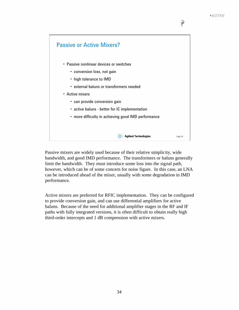
Passive mixers are widely used because of their relative simplicity, wide bandwidth, and good IMD performance. The transformers or baluns generally limit the bandwidth. They must introduce some loss into the signal path, however, which can be of some concern for noise figure. In this case, an LNA can be introduced ahead of the mixer, usually with some degradation in IMD performance.
Active mixers are preferred for RFIC implementation. They can be configured to provide conversion gain, and can use differential amplifiers for active baluns. Because of the need for additional amplifier stages in the RF and IF paths with fully integrated versions, it is often difficult to obtain really high third-order intercepts and 1 dB compression with active mixers.
35
H•4/17/01
Page 35
Mixer circuit examples
• OK, now let’s look at some examples
• 2 mixer circuits will be reviewed:
• diode DB quad:
• familiar and widely used
• wide bandwidth, limited by baluns
• Low IMD FET mixer:
• not as well known, but good performance

36
H•4/17/01
Page 36
Diode DB quad mixer
+ LO− LO
LOVIF
VRF(t)
VLO(t) VRF(t)
VIF(t)
The diode double-balanced quad mixer is a very popular design and available in a wide variety of frequency bandwidths and distortion specs. The MiniCircuits™ catalog [7] is full of these. The diodes act as a polarity reversing switch as seen in the bottom of the figure. When the top of the LO transformer is positive, the blue path is conductive and will ground the top of the RF transformer. When the top is negative, the red path is conducting and the RF polarity reverses. Both LO and RF feedthrough are suppressed by the symmetry and balancing provided by the transformers. The LO signal at the RF and IF ports appears to be a virtual ground for either LO polarity.
Since the LO signal must switch the diodes on and off, a large LO power is required, typically 7 dBm when one diode is placed in each leg, 17 dBm with two diodes per path! With this much LO power, even with good isolation, there may still be significant LO in the IF output.
When the diodes are conducting with LO current >> RF current, the mixer should behave linearly. At large RF signal powers, the RF voltage modulates the diode conduction, so lots of distortion will result in this situation. The diodes are also sensitive to RF modulation when they are biased close to their threshold current/voltage. For both reasons, we prefer high LO drive with a fast transition (high slew rate - a square wave LO is better than sine wave) between on and off. The IMD performance is very poor with small LO power.

37
H•4/17/01
Page 37
Design procedure
• Determine correct RF and LO impedances to match through the diode ring to the 50 ohm IF load. Transformer ratios can be swept using HB or XDB.
• Sweep LO power to maximize conversion gain and gain compression
• Or, buy one from MiniCircuits™!
The RF and LO impedances at the diode ring theoretically should be determined and matched at all of the relevant harmonics. [8] For most designs, optimizing the transformer ratios with the IF port connected to 50 ohms should be sufficient, since we cannot select impedances at each frequency independently, and this approach would not be possible for a broadband design such as this.
Exercise 4. Modify the gain compression simulation (diodeDBQ_GC) to evaluate conversion gain and P1dB as a function of LO power. Use the XDB simulator with a parameter sweep. (solution: ADS file diodeDBQ_ex4)
Exercise 5. Sweep the RF transformer turns ratio to find the best ratio for conversion gain and P1dB. (solution: ADS file diodeDBQ_GC_OPT)

38
H•4/17/01
Page 38
Diode mixer performance
2-tone
1-tone
P1dB = + 5 dBmP1dB = 0 dBm
A harmonic balance simulation can be used to estimate the mixer performance. With the DB diode mixer, the currents in the diodes are half wave, so a highnumber of LO harmonics and maximum order and some oversampling of the FFT operation are necessary to reproduce this waveform and therefore get reasonable accuracy on the third-order product. Gain compression is not as sensitive to the LO order.
Gain compression behavior depends strongly on the signal statistics as discussed earlier. There is about 5 dBm difference in P1dB between single and two tone simulations.
We see that the third order IMD predictions are not “well behaved”; the slope is 33.2 dB/decade instead of 30. This puts our TOI calculation in doubt, but it is still useful for design optimizations. We can also see that the OIP3 prediction depends upon the RF input power level.
Noise figure of these passive switched mixers is usually close to
NF = − ConvGainThus, for a -5 dB Conversion Gain, a noise figure of about 5 dB is expected.
[See ADS example files diodeDBQ_TOI and diodeDBQ_GC]

39
H•4/17/01
Page 39
Need good match at each port
VRF(t)
VLO(t)
IF
Image, HD, IMDRF
IF term P1dB TOI50Ω 0 dBm 15 dBmBPF −2 −2
Since these passive diode switch mixers are bilateral, that is, the IF and RF ports can be reversed, the performance of the mixer is very sensitive to the termination impedances at all ports. A wideband resistive termination is needed to absorb not only the desired IF output but also any images, harmonics, and IMD signals. If these signals are reflected back into the mixer, they will remix and show up at the RF port and again at the IF port. The phase shifts associated with the multiple replicas of the same signals can seriously deteriorate the IMD performance of the mixer.
A simulation was carried out using a bandpass filter in the IF port as shown above. The P1dB was degraded by 2 dB and the third-order IMD power was not well behaved. A calculated TOI showed nearly 17 dB degradation.
Thus, it is important to terminate. Terminations can consist of:
1. Attenuator. Obviously not a good idea if NF is important
2. Wideband amplifier with good S11 or S22 return loss
3. Diplexer. A passive network that separates frequencies but
provides Zo termination for all components.
[See ADS example file: diodeDBQ_TOI_BPF]

40
H•4/17/01
Page 40
Mixer termination methods
• Passive diplexer
RF
LO
IF
series resonant at FIF
parallel resonantat FIF
50
50
LO, RF harmonics, feedthrough, IMD
out of bandreflections
This passive diplexer provides a low-loss forward path through the series resonant branch. At FIF, the parallel resonant branch has a high impedance and does not load the IF. Outside of the IF band (you need to set the Q for the design to control the bandwidths) the series resonant branch presents a high impedance to the signals and the parallel resonant branch a low, but reactive impedance. At these frequencies, above (through C) and below FIF (through L), the resistors terminate the output. The farther away from FIF you are, the better the match.

41
H•4/17/01
Page 41
Mixer termination methods
• Active wideband termination
RF
LO
Zin ≈ 1/gm gm ≈ IC/VT
This common base stage provides a wideband resistive impedance provided the maximum frequency at the input is well below the fT of the transistor. The bias current can be set to provide a 50 ohm input impedance. Alternatively, one can bias the device at higher current levels and add a series resistor at the input. Of course, this degrades noise, but will improve IMD performance. The amplifier must be capable of handling the complete output power spectral density of the mixer without distorting.

42
H•4/17/01
Page 42
Low IMD FET mixer
RF IF
LO
VT
• LO modulates channel resistance
• Channel resistance is very linear at small VDS
• LPF and HPF act as diplexerHPF LPF
Another popular mixer utilizes only one FET in its simplest form. [10] The LO signal switches the FET on and off. The gate is biased close to threshold. The channel resistance of the FET therefore becomes time dependent and provides a switching mixer behavior. The RF input and IF output are separated by high pass (HPF) and low pass (LPF) filters respectively.
The surprising thing about this design is the high P1dB and TOI that it can deliver. On the down side, one must do some balancing to get rid of significant LO to IF feedthrough.

43
H•4/17/01
Page 43
ID - VDS of MOSFET
• Highly linear at low VDS
• Device width and LO voltage can be optimized for performance
The mixer RF to IF path will be quite linear if the total drain voltage (VDS) remains small. As can be seen from the DC simulation, the MOSFET exhibits quite linear channel resistance up to at least a VDS of + and - 0.25V.
[See ADS example files: MOSFET_IVtest]

44
H•4/17/01
Page 44
Design process
• Select nominal FET channel width and optimize the source and load impedances for conversion gain
• Design input (HPF) and output (LPF) networks which present theseimpedances to the FET drain
• Optimize FET width and matching impedances for highest P1dB
The design procedure for this mixer requires that the optimum impedances be presented to the RF and IF ports where they join at the drain. These networks can also act as diplexer to some degree, helping to separate RF from the IF output and vice-versa. A 1-port impedance block can be placed in each path and ADS used to optimize the conversion gain. These impedances will provide an initial estimate of the optimum RF and IF impedances. Alternatively, a current probe can be placed in series with the RF and IF paths to the drain. The V/I at each connection can be analyzed at each frequency and optimum impedances inferred.
Next, high-pass and low-pass networks can be designed to present these impedances, at least at the fundamental frequencies. ADS can again be used to optimize the conversion gain. Device width may also be varied to improve P1dB.
[See ADS design files: fet1opt1tone and fet1optmatch]

45
H•4/17/01
Page 45
FET mixer performance
Conv Gain (1 tone input)Conv Gain (2 tone input)
P1dB = + 12 dBmP1dB = + 7 dBm
The mixer performance was simulated. Surprisingly, we see that the P1dB is higher than that simulated for the diode mixer. The OIP3 is also reasonably high.
[See ADS design files fet1_GC, fet1_GC2 and fet1_TOI]
46
H•4/17/01
Page 46
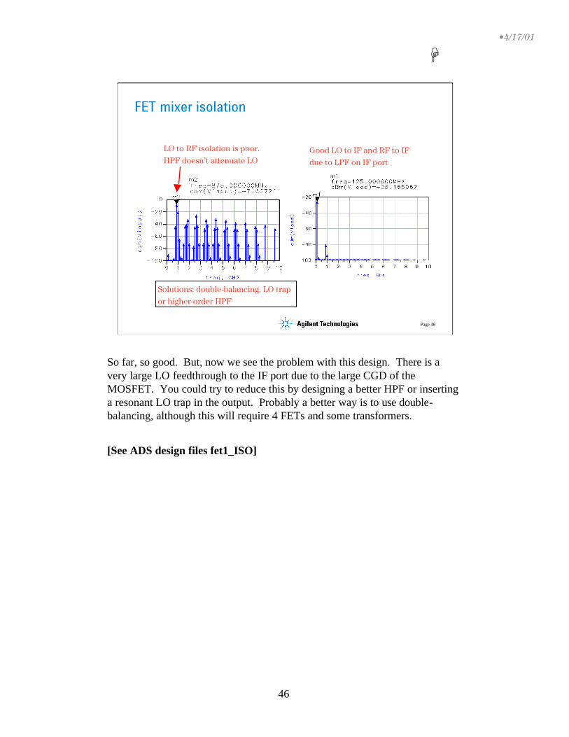
FET mixer isolation
LO to RF isolation is poor.HPF doesn’t attenuate LO
Good LO to IF and RF to IFdue to LPF on IF port
Solutions: double-balancing, LO trapor higher-order HPF
So far, so good. But, now we see the problem with this design. There is a very large LO feedthrough to the IF port due to the large CGD of the MOSFET. You could try to reduce this by designing a better HPF or inserting a resonant LO trap in the output. Probably a better way is to use double-balancing, although this will require 4 FETs and some transformers.
[See ADS design files fet1_ISO]

47
H•4/17/01
Page 47
Conclusion
• Understand operating principles of the mixer
• What makes a good mixer?
• Choices: nonlinear/switching mode; single/double balance; active/passive
• Specify performance: Gain, NF, P1dB, TOI, SFDR, isolation
• Mixer examples - numerous other possibilities
Learning objectives:

48
H•4/17/01
Page 48
Exercises1. Use ADS to evaluate the performance of a single-balanced or
double-balanced FET mixer based on the mixer example in this seminar. You will need to add transformers to do this. Evaluate and compare the conversion gain, isolation, P1dB, and TOI with the single FET version.
• Go through the ADS example files, modify them for your own design work.
Further resources:

49
H•4/17/01
Page 49
Exercises
VRF(t)
VIF(t)
VLO(t)
VGG
2. Refer to the notes page...
The mixer shown above is the FET equivalent of the diode ring mixer. This was first described by Ed Oxner [10] and can provide impressive large signal performance with a sufficiently strong LO voltage. The substrate connection of the MOSFETs can be grounded or connected to a negative supply to reduce the gate capacitances.
Using the MOSFET model from the previous ADS examples, design this mixer and evaluate all of the important mixer performance measures.
[10] Oxner, E. S., “Commutation Mixer Achieves High Dynamic Range,” RF Design, pp. 47-53, Feb. 1986.

50
H•4/17/01
Page 50
References
• [1] Gray, P. R. and Meyer, R. G., Design of Analog Integrated Circuits, 3rd Ed., Chap. 10, Wiley, 1993.
• [2] Gilbert, B., “Design Considerations for BJT Active Mixers”, Analog Devices, 1995.
• [3] Lee, T. H., The Design of CMOS Radio-Frequency Integrated Circuits, Chap. 11, Cambridge U. Press, 1998.
• [4] Hayward, W., Introduction to Radio Frequency Design, Chap. 6, American Radio Relay League, 1994.
• [5] Razavi, B., RF Microelectronics, Prentice-Hall, 1998.
• [6] Maas, S., “Applying Volterra Series Analysis,” Microwaves and RF, p. 55-64, May 1999.
• [7] Minicircuits RF/IF Designers Handbook, www.minicircuits.com
• [8] Maas, S., “The Diode Ring Mixer”, RF Design, p. 54-62, Nov. 1993.
• [9] Maas, S., “A GaAs MESFET Mixer with Very Low Intermodulation,” IEEE Trans. on MTT, MTT-35, pp. 425-429, Apr. 1987.
References[1] Gray, P. R. and Meyer, R. G., Design of Analog Integrated Circuits, 3rd Ed., Chap. 10, Wiley, 1993.
[2] Gilbert, B., “Design Considerations for BJT Active Mixers”, Analog Devices, 1995.
[3] Lee, T. H., The Design of CMOS Radio-Frequency Integrated Circuits, Chap. 11, Cambridge U. Press, 1998.
[4] Hayward, W., Introduction to Radio Frequency Design, Chap. 6, American Radio Relay League, 1994.
[5] Razavi, B., RF Microelectronics, Prentice-Hall, 1998.
[6] Maas, S., “Applying Volterra Series Analysis,” Microwaves and RF, p. 55-64, May 1999.
[7] Minicircuits RF/IF Designers Handbook, www.minicircuits.com
[8] Maas, S., “The Diode Ring Mixer”, RF Design, p. 54-62, Nov. 1993.
[9] Maas, S., “A GaAs MESFET Mixer with Very Low Intermodulation,” IEEE Trans. on MTT, MTT-35, pp. 425-429, Apr. 1987.

51
H•4/17/01
Page 51
End of Design Seminar...

www.agilent.com/fi nd/emailupdatesGet the latest information on the products and applications you select.
www.agilent.com/fi nd/agilentdirectQuickly choose and use your test equipment solutions with confi dence.
Agilent Email Updates
Agilent Direct
www.agilent.comFor more information on Agilent Technologies’ products, applications or services, please contact your local Agilent office. The complete list is available at:www.agilent.com/fi nd/contactus
AmericasCanada (877) 894-4414 Latin America 305 269 7500United States (800) 829-4444
Asia Pacifi cAustralia 1 800 629 485China 800 810 0189Hong Kong 800 938 693India 1 800 112 929Japan 0120 (421) 345Korea 080 769 0800Malaysia 1 800 888 848Singapore 1 800 375 8100Taiwan 0800 047 866Thailand 1 800 226 008
Europe & Middle EastAustria 0820 87 44 11Belgium 32 (0) 2 404 93 40 Denmark 45 70 13 15 15Finland 358 (0) 10 855 2100France 0825 010 700* *0.125 €/minuteGermany 01805 24 6333** **0.14 €/minuteIreland 1890 924 204Israel 972-3-9288-504/544Italy 39 02 92 60 8484Netherlands 31 (0) 20 547 2111Spain 34 (91) 631 3300Sweden 0200-88 22 55Switzerland 0800 80 53 53United Kingdom 44 (0) 118 9276201Other European Countries: www.agilent.com/fi nd/contactusRevised: March 27, 2008
Product specifi cations and descriptions in this document subject to change without notice.
© Agilent Technologies, Inc. 2008
For more information about Agilent EEsof EDA, visit:
www.agilent.com/fi nd/eesof