preliminary technical program - society of vacuum coaters
TRANSCRIPT

Preliminary
› WebTech Roll to Roll Coatings for High-End Applications
› Coatings for Cleantech Energy Conversion, Storage and Related Processes
› Tribological and Decorative Coating› Emerging Technologies› High Power Impulse Magnetron Sputtering› Optical Coating
› Vacuum Processes and Coatings for Biomedical Applications
› Large Area Coating› Plasma Processing› Heuréka! Post-Deadline Recent Developments› Business Topics Session› Technical Poster Presentations
Traditional sessions examine proven technologies applied to unique processes and applications:
Technology Exhibit: May 1–2Technology and business intersect in Santa Clara! This 2-day event, dedicated to vacuum coating
technology, offers the ideal location to meet new customers and connect with existing clients. See page 28 ››
Technical Program
Explore the Science and TechnologyDriving Future Innovation
Featuring Symposia topics that are integral parts of our traditional Technical Program:
“Lab to Fab” Vacuum Coating Manufacturing Processes
New Materials and Processes for Photovoltaics Manufacturing
Technical Program Two-day Exhibit Tutorial Courses Networking
Tutorial Courses: April 28–May 3This year’s lineup includes new Hot Topic Tutorials designed to complement the Technical Program
content and Exhibit. See page 16 for the 2012 Tutorial Roster ››
Technical Program: April 30–May 3
55th 2012 SVC Annual Technical Conference April 28–May 3, 2012 | Santa Clara Convention Center, Santa Clara, California USA

Society of Vacuum Coaters » 2012 TechCon Preliminary Program 2
2012 Conference Overview
2
The Society of Vacuum Coaters TechCon is “the place to be” to interact and network with individuals at all levels of product development and production. The latest in vacuum coating and related tech-nologies, and their role in high tech applications are explored.
The TechCon is about taking physical vapor deposition (PVD) materials and processes that are devel-oped in the laboratory and scaling them up to meet commercial applications at a viable cost. To this end the conference has technical papers that span the spectrum from academia and R&D laborato-ries – to high rate, high yield, low cost production – to market analysis. Reaching these goals requires both basic knowledge of the materials and processes involved but also the equipment engineering and the process monitoring and control necessary for high rate, high yield, and low cost production.
Of particular interest is how best to match production and product requirements to the many avail-able options for PVD. In vacuum deposition processes both vacuum and plasma environments are used so basic and applied knowledge of these processing environments is necessary. In addition, other aspects of surface engineering are addressed such as plasma-surface modification, duplex processes such as combinations of PVD and Chemical Vapor Deposition (CVD), and the cleaning of surfaces is addressed.
This year, in addition to 12 traditional Technical Sessions, the SVC TechCon offers two Symposia that are timely to the needs of the market place. These Symposia are important reasons to attend this conference.
Symposia Topics Link Innovation with BusinessThe Symposium on Materials and Processes for Photovoltaics and Manufacturing addresses how thin film voltaics are meeting a challenge as the cost of wafer-based PV continues to decline. New materi-als that can be used within large area coating processes are promising, and the Symposium will look at how this can help move manufacturing from low quality devices to large area coating of commer-cially important high quality devices. The emphasis will be on new materials, processes (including “green” processes), new production technologies for large area high-yield manufacturing, device performance, and fabrication limitations, as well as road mapping and scaling-up for these materials and processes. The keynote presentation by Professor Eicke Weber will shed light on new materials for Photovoltaics.
The Symposium on “Lab to Fab” Vacuum Coating Manufacturing Processes focuses on the transition from a lab-scale material or process to manufacturing – and this can be a huge challenge. The SVC offers unmatched expertise in thin film processes and large area manufacturing to the Silicon Valley and has assembled a group of speakers for the Symposium who will highlight the pitfalls and traps that are encountered when moving to a large-scale manufacturing environment. The Symposium will emphasize developing technology markets in the areas of Nanotechnology, Touch Panels, Flexible Electronics, Energy Storage and Energy Saving Technologies, and Solid State Lighting. The keynote presentation by Robert Praino provides an insight to issues relating to the Lab to Market Transition.
Traditional Technical Sessions explore updates in topics of vital importance to the vacuum coating industry:• WebTechRolltoRollCoatingsforHigh-EndApplications• CoatingsforCleantechEnergyConversion,StorageandRelatedProcesses• TribologicalandDecorativeCoating• EmergingTechnologies• HighPowerImpulseMagnetronSputtering• VacuumProcessesandCoatingsforBiomedicalApplications• OpticalCoating• LargeAreaCoating• PlasmaProcessing• Heureka!Post-DeadlineRecentDevelopments• BusinessTopicsSession• TechnicalPosterPresentations
AnewdynamictotheSVCTechConin2012isanExecutive Forum on Road Mapping of Future Thin Film Products.Anopeninteractionbetweencaptainsofindustryandtheattendeeswilllookatfuture products involving thin film technology, their markets and how to get there. Michael Lebby, GeneralManagerandCTOofTranslucentInc.andBettinaWeiss,ExecutiveDirector,SEMIPVGroupwill provide personal insights into important future developments.
85% Sold Out as of Year EndThis business-friendly environment has been crafted to provide learning, networking and business opportunities for all TechCon participants. In addition to a global collection of manufacturers and suppliers of vacuum de-position equipment, analytical equipment and components, the Exhibit is the perfect venue for networking opportunities for those seeking information on our technology and those who canoffersolutions.Readmoreaboutthe2012Exhibit on pages 28 and 29.
Designed to complement the TechCon Techni-cal Program Sessions and Exhibit, the six-day Education Program includes six new full and half-day tutorials. Twenty-six tutorials will be offered in Santa Clara, with the new tutorials highlightinghottopicswithintheindustry.Alist of the tutorials offered at the TechCon is found on page 16; course descriptions begin on page 17.
Wolfgang Decker, VAST Films Ltd., Darlington, PA (724/827-8827, [email protected]) is the Program Chair. Scott Walton, U.S. Naval Research Laboratory (202/767-7531, [email protected]) is the Assis-tant Program Chair. Ladislav Bardós, Uppsala University, Uppsala, Sweden (46/184 7130 34, [email protected]) is the Past Program Chair. Carl M. Lampert, Star Science (707/794-0333, [email protected]) is the SVC Technical Director.
What is the SVC Technical Conference All About?Finding Solutions. Making Connections.
The Technical Program The Technology Exhibit
The Education Program

3505/856-7188 Fax 505/856-6716 » E-mail [email protected] » Web Site www.svc.org
2012 Technical Program
3505/856-7188 Fax 505/856-6716 » E-mail [email protected] » Web Site www.svc.org
Table of ContentsConference Overview . . . . . . . . . . . . . . . . . . . . . . . .2Welcome Reception . . . . . . . . . . . . . . . . . . . . . . . . . 32012 Technical Program . . . . . . . . . . . . . . . . . 4-15Technology Forum Breakfasts . . . . . . . . . . . . . 5, 8Donald M . Mattox Tutorial Program . . . . . 6, 14SVC Foundation 5K Fun Run and Walk . . . . . . .9“Meet the Experts” Corner . . . . . . . . . . . . . . . 10, 13A Wizard’s Guide to Understanding Vacuum and Vacuum Coating . . . . . . . . . . 11Education Program Schedule . . . . . . . . . . . . . . 16Tutorial Courses and Instructors . . . . . . . . 17-27SVC Networking Events . . . . . . . . . . . . . . . . . . . . 20SVC On Location Education Program . . . . . . . . . . . . . . . . . . . . . . . . . . . . . . . . 242012 SVC Exhibit and Target Marketing . . . . . . . . . . . . . . . . . . . . . . . . . . . . . . 28Corporate Sponsors . . . . . . . . . . . . . . . . . . . . . . . . 29Conference Registration Information . . . 30-312012 TechCon Sponsors . . . . . . . . . . . . . . . . . . . . 32
Weekend at a Glance
S AT u r d AyEducation ProgramFullDayTutorials8:30a.m.–4:30p.m.• VacuumSystems,MaterialsandOperation• AnIntroductiontoPhysicalVaporDeposition
(PVD) Processes• ThinFilmGrowthandMicrostructure
Evolution• ZincOxide-BasedandOtherTCOAlternatives
to ITO: Materials, Deposition, Properties and Applications
S u n d AyEducation Program• SputterDeposition(day1of2)(FullDay)• OpticalCoatingDesign(FullDay)• HighPowerImpulseMagnetronSputtering
HIPIMS(FullDay)• UnderstandingSolarCells(AM)• IntroductiontoThinFilmPhotovoltaic
Technologies (PM)
Special Events• SVCFoundationGolfTournament-12:00p.m.• YoungMembersGroup/MentorsProgram
5:00p.m.–6:30p.m.• WelcomeReception7:00p.m.
SVC young Members Group/Mentors Program Sunday evening, April 29, 5:00 p.m. – 6:30 p.m.Amentoringprogramisbeingofferedatthe2012TechConforYoungMembersandstudents,andisdesigned to offer participants the opportunity to engage in one-on-one discussions with volunteer mentors from industry and academia within various sectors of the vacuum coating community.
Theinformalmentoringprogramservesasa“bridge”betweenYoungMembers,studentsandmen-tors within the Society, providing a venue for connecting with those working in specific areas of vacuum coating. Focused discussions explore technical issues, employment opportunities in vacuum coating and surface technologies, and offer useful knowledge on how to successfully navigate the conference.
TheYoungMembersGroupisopentoyoungpeoplewithaninterestinvacuumcoatingandrelatedtechnologies. Members of the group may be students or young professionals or technical staff in industry; the common feature is that they should meet the age requirement (under 31 years of age at anytimein2012)andhaveakeeninterestinanyofthetopicsthatsitundertheumbrellaoftheSVC.
Young Members receive the following discounts: •DiscountedMembershipFeeof$40 •DiscountedConferenceRegistrationFeeof$225
FormoreinformationontheYoungMembersGroupandMentorsProgram,visitwww.svc.organdexploretheStudentsandYoungMembersbutton.Alistofmentors,includingtheirprofessionalaf-filiation and area of expertise, is available for anyone seeking to make connections prior to attending the TechCon in Santa Clara.
registration is now OpenWe had a record number of Exhibit Visitors at the2009TechConinSantaClara,andarework-ing very hard to attract even more interest in 2012.Thisyear’stechnicalprogramisrenewedwith traditional topics examining proven technologies applied to unique processes and applications. Plus, the Symposia topics focus on particular hot topics and issues of interest to individuals and industries using vacuum coating processes. Online registration for the TechConandtheHotelReservationsystemisnow open at www.svc.org.
SVC Headquarters Hotel: Hyatt Regency Santa Clara $175.00 single/doubleplustaxes;GovernmentRate rooms available
Hilton Santa Clara $175.00 single/doubleplustaxes
Biltmore Hotel & Suites, Santa Clara $135.00TowerSuiterooms;single/double occupancy plus taxes
Welcome receptionSunday Evening, April 29 at 7:00 p.m.EveryoneisinvitedtoattendtheWelcomeReceptiononSundayevening.Alwaysoneofthemostpopular networking events at the annual conference, this event offers a relaxed venue for friends and colleagues to reconnect before the start of the Technical Program on Monday morning. The reception will include a light dinner buffet and live music for dancing. Please indicate when regis-tering if you will be attending this event.
Hyatt Regency Convention Center

Society of Vacuum Coaters » 2012 TechCon Preliminary Program 4
2012 Technical Program
Monday Morning, April 30Technology Forum Breakfast7:00a.m.–8:15a.m.
Facilitator-led round table discussions provide an opportunity for information, conversation and interaction on specific subjects. See page 5 for topics and facilitators .
Keynote Presentation8:30 a.m. – 9:10 a.m.
new Materials and Processes for Photovoltaics ManufacturingPresented by Professor Eicke Weber, Fraunfoher Institute for Solar Energy Systems ISE, Freiberg, Germany and Faculty of Physics and Mathemat-ics, and Faculty of Engineering, Albert-Ludwigs University, Freiburg, Germany See abstract and biographical sketch on this page .
Symposium on New Materials and Processes for Photovoltaics ManufacturingModerator: Wolfgang Diehl, Fraunhofer Insti-tute for Surface Engineering and Thin Films IST, Germany
9:10 a.m. PV-1 Metallic Sputtering Targets for CIGS Thin Film Photovoltaics C.Adelhelm,E.Franzke,H.Koestenbauer,C.Linke, and J. Winkler,PLANSEESE,Reutte,Austria
Contributed by the Coatings for Cleantech Energy Conversion, Storage and Related Processes TAC 9:30 a.m PV-2TechnicalBarriersinManu-facture of CIGS Thin Film Solar Cells R. Noufi, National Center for Photovoltaics, Na-tional Renewable Energy Laboratory, Golden, CO
10:10 a.m. – 10:30 a.m. – Break
10:30 a.m. PV-3 Linear Thermal Evaporation SourceforLargeAreaCIGSSolarCellManufac-turing K.Zhang and R. Faber, Vacuum Process Tech-nology,LLC,Plymouth,MA
10:50 a.m. PV-4IndustrialSizeReactiveMag-netronSputteringofZnO:AlUsingRotatableZn:AlTarget V. Linss,VONARDENNE,Dresden,Germany
11:10 a.m. PV-5 Comparative Reactive and Non-ReactiveAZODepositionUsingAsymmet-ric Rotatable Magnetron Technology D. Monaghan,R.Brown,V.Bellido-Gonzalez,andM.Audronis,GencoaLtd,Liverpool,UnitedKingdom;andS.Williams,GencoaUSA,SanFrancisco,CA
11:30 a.m. PV-6PlasmaDepositedZnOLayers for Thin Film Photovoltaics: Synthesis, Characterization and Growth Mechanism M. Creatore,H.C.M.Knoops,M.Ponomarev,M.C.M.vandeSanden,andW.M.M.Kessels,DepartmentofAppliedPhysics,Eindhoven
KeynoteSpeaker
Symposium on new Materials and Processes for Photovoltaics ManufacturingMonday Morning, April 30 at 8:30 a.m.
New Materials and Processes for Photovoltaics ManufacturingPresented by Professor Eicke R. Weber, Director, Fraunhofer Institute for Solar Energy Systems ISE, Freiburg, Germany and Faculty of Physics and Mathematics, and Faculty of Engineering, Albert-Ludwigs University, Freiburg, Germany
In recent years, Europe and especially Germany, has taken a leading posi-tion in the implementation of PV power. This has also spurred rapid progress in materials research and production technology development. Today’s PV market is dominated by solar cells made out of crystalline silicon with solar power conversion efficiencies in the 15-21% range. Research here is focused on new, high-efficient and cost-effective cell architectures such as laser-based
contacting and processing. Solar silicon with higher impurity content than Si used for microelectron-ics has been proven to be a cost-effective new material providing similar cell efficiencies. About 15% of the current PV market are thin film technologies based on amorphous or microcrstalline silicon or SiGe heterostructures, CdTe, or CuIn(Ga)S. Thin-film PV has the lowest cost per installed Watt, with CdTe PV modules soon reaching a price of $1/Wp. A decisive increase in market share is hampered by the rather low efficiency of these modules in the 8–11% range. Here, the key challenge is to transfer the impressive lab results of small cells, with efficiencies reaching 18%, to a reliable, mass-production module level. Thin film silicon is as well showing impressive progress by using micromorph structures, deposition on inexpensive multicrystalline substrates or SiGe heterostructures. A third technology that is just entering the market on a large scale is based on high-efficiency III/V multijunction hetero-structures, reaching efficiencies above 40% under high concentration. Organic, or dye-sensitized cells, and PV cells based on nanostructures as active layer still are limited by very low efficiencies in the 2-5% range, but provide very exciting research topics all over the world. This talk will discuss recent progress in introducing new materials and new processing techniques for photovoltaics, an exciting and important global market soon to reach more than $100 billion annual volume.
The focus of Professor Weber’s research is the analysis of lattice defects in Si and compound semiconductors. Recently he studied specifically how good solar cells can be produced out of upgraded metallurgical (“dirty”) silicon with high impurity content. In 1994 he received an Alexander von Humboldt Senior Scientist Award. From 2004-2006 he served as the chair of the Nanoscale Science and Engineering Graduate Group in Berkeley. He was president of the Alexander von Humboldt Association of America (AvHAA) from 2001-2003 and in 2003 he was elected founding president of the German Scholars Organization (GSO). In 2006 he received the Award of Merit (Bundesverdienstkreuz am Bande) of the German President. He is fellow of the American Physical Society. In July 2008 Professor Weber was appointed Director to the SEMI International Board of Directors. He received the Electronics and Photonics Division Award of the Electrochemical Society ECS in June 2009. In October 2009 he was elected Honorary Member of the Ioffe Physical-Technical Institute of the Russian Academy of Sciences, St. Petersburg. Since 2010 Professor Weber is Member of acatech - the German Academy of Science and Engineering, Berlin.
KEynOTE SPEAKEr
INVITEDSPEAKER
Monday at a Glance
M O r n i n GTechnical Sessions •KeynotePresentation8:30a.m. •Symposium on New Materials and Processes for Photovoltaics Manufacturing •TribologicalandDecorativeCoating •PlasmaProcessing
Special Events •TechnologyForumBreakfast7:00a.m.–8:15a.m.
Education Program FullDayTutorials8:30a.m.–4:30p.m. •SputterDeposition(day2of2) •SputterDepositionontoFlexibleSubstrates •CharacterizationofThinFilms •PracticalAspectsofOpticalCoatings
A F T E r n O O nTechnical Sessions •DonaldM.MattoxTutorial12:50p.m.–1:10p.m. •KeynotePresentation1:50p.m. •Symposiumon“LabtoFab”VacuumCoating Manufacturing Processes •LargeAreaCoating •HighPowerImpulseMagnetronSputtering– HIPIMS •EmergingTechnologies •Heuréka!(Evening–6:00p.m.)
Special Events •AnnualBusinessMeeting12:20p.m.

5505/856-7188 Fax 505/856-6716 » E-mail [email protected] » Web Site www.svc.org
2012 Technical Program
UniversityofTechnology,Eindhoven,TheNetherlands
11:50 a.m. PV-7NewApproachesofControl-ling of Electrical and Optical Properties of DC SputteredAlDopedZnOThinFilmforTranspar-ent Conducting Oxide W.YangandJ.Joo,KunsanNationalUniversity,Kunsan,SouthKorea
Tribological and decorative CoatingModerators:JolantaKlemberg-Sapieha, École Polytechnique de Montréal, Canada andKlausBewilogua,Fraunhofer Institute for Surface Engineering and Thin Films IST, Germany
INVITEDSPEAKER9:10 a.m. T-1 In Situ Tribometry: Shedding LightontheTribologyofHardCoatings R.R. ChromikandH.W.Strauss,DepartmentofMiningandMaterialsEngineering,McGillUni-versity,Montréal,Canada;andS.HassaniandJ.E.Klemberg-Sapieha,ÉcolePolytechniquedeMontréal,Montréal,Canada
9:50 a.m. T-2 Properties of TiN Films Pre-paredbyObliqueAngleDeposition J.I. Jeong,J.H.Yang,J.H.Jung,H.S.Park,andM.A.Song,HybridMaterialsResearchDepart-ment, Research Institute of Industrial Science andTechnology,Pohang,Korea
10:10 a.m. – 10:30 a.m. – Break
10:30 a.m. T-3DepositionofThicka-C:H:SiCoatingsforTribologicalApplications C. Forsich,UniversityofAppliedSciences,Wels,Austria;D.Heim,UpperUniversityofAppliedSciences,Wels,Austria;andT.MuellerandA.Gebeshuber,RübigGmbH&CoKGAnlagen-technik,Wels,Austria
10:50 a.m. T-4SiliconAluminumOxynitrideThin Films Deposited by Plasma Enhanced Chemical Vapour Deposition Sponsored Student Presentation O. Taggart and P. Masher, Department of Engi-neeringPhysics,McMasterUniversity,Hamilton,Canada; L. Martinu, Department of Engineering Physics,ÉcolePolytechniquedeMontréal,Mon-tréal,Canada;J.Wojcik,DepartmentofEngi-neeringPhysics,McMasterUniversity,Hamilton,Canada;J.E.Klemberg-Sapieha,DepartmentofEngineeringPhysics,ÉcolePolytechniquedeMontréal,Montréal,Canada
11:10 a.m. T-5HighPerformancePVDCoatingsforToday’sandTomorrow’sEnginePlatforms R. Jacobs,HauzerTechnoCoatingBV,Venlo,TheNetherlands;T.LiskiewiczandL.Austin,SchoolofMechanicalEngineering,UniversityofLeeds,Leeds,UnitedKingdom;D.DoerwaldandR.Tietema,HauzerTechnoCoatingBV,Venlo,TheNetherlands;A.Neville,SchoolofMechanicalEngineering,UniversityofLeeds,Leeds,UnitedKingdom;andT.Krug,HauzerTechnoCoatingBV,Venlo,TheNetherlands
11:30 a.m. T-6 Nanostructured PVD Coating for HighDemandedApplications J.A.Araujo, Metallurgical and Materials Engi-neeringDepartment,UniversityofSãoPaulo,SãoPaulo,Brazil;G.M.Araujo,MAHLE-Tech-nologyCenterBrazil,SãoPaulo,Brazil;andA.Tschiptschin, Department of Metallurgical and MaterialsEngineering,SãoPauloUniversity,SãoPaulo,Brazil
11:50 a.m. T-7 Modified Diamond-Like Carbon Multilayer Coatings on Metallic Substrates ProducedbyPulsed-DCHollowCathodePECVD Sponsored Student PresentationR.BirneyandF.Placido,ThinFilmCentre,Uni-versityoftheWestofScotland,Paisley,UnitedKingdom
Plasma ProcessingModerators: JamesBradley,University of Liverpool, United Kingdom and Jorg Patscheider, EMPA, Switzerland
9:10 a.m. P-1 Effects of Cumulative Surface Treatment on Vacuum-Deposited Coating Adhesion R. Wolf, Enercon Industries Corporation, MenomoneeFalls,WI;C.A.Bishop,C.A.BishopConsultingLtd,NearLoughborogh,UnitedKingdom;andI.Fletcher,IntertekMSG,Redcar,UnitedKingdom
9:30 a.m. P-2 Influence of Deposition Param-etersinPACVD-SiO2 Preparation on Resulting Film Properties R.Bandorf, Fraunhofer Institute for Surface EngineeringandThinFilmsIST,Braunschweig,Germany; I. Stasewitsch, Insitut für Oberflächen-technik,TU-Braunschweig,Braunschweig,Germany;H.Gerdes,FraunhoferInstituteforSurfaceEngineeringandThinFilmsIST,Braun-schweig,Germany;andG.Bräuer,FraunhoferInstitute for Surface Engineering and Thin Films IST,Braunschweig,GermanyandInsitutfürOberflächentechnik,TU-Braunschweig,Braun-schweig, Germany
9:50 a.m. P-3Plasma-BasedChemicalModifi-cation of Epitaxial Graphene S.C.Hernández,M.Baraket,andE.H.Lock,PlasmaPhysicsDivision,U.S.NavalResearchLaboratory, Washington, DC; V.D. Wheeler, L.O. Nyakiti,F.J.Bezares,R.L.Myers-Ward,C.R.EddyJr.,D.K.Gaskill,andJ.D.Caldwell,ElectronicsScienceandTechnologyDivision,U.S.NavalResearch Laboratory, Washington, DC; and S.G. Walton,PlasmaPhysicsDivision,U.S.NavalResearch Laboratory, Washington, DC
10:10 a.m. – 10:30 a.m. – Break
10:30 a.m. P-4MagnetronAssistedPECVDPro-cessforDepositionofa-Si:Handµc-Si:HfromaSilane-Hydrogen-ArgonGasMixture P. Pötschick,H.Bartzsch,A.Delan,andP.Frach,FraunhoferInstituteforElectronBeamandPlasma Technology FEP, Dresden, Germany
10:50 a.m.P-5AlternativeMethodsforDeposi-tion of Superhydrophobic Fluorocarbon Coatings H.Biederman,O.Kylian,M.Petr,M.Drabik,A.Serov,O.Polonskyi,P.Solar,A.Artemenko,A.Choukourov,J.Kousal,D.Arzhakov,andD.Slavinska,CharlesUniversityinPrague,Prague,Czech Republic
11:10 a.m. P-6 Nanorough Surfaces Prepared UsingGasAggregationClusterSources Sponsored Student Presentation P. Solar,O.Polonskyi,M.Petr,O.Kylian,A.Artemenko,A.Choukourov,D.Arzhakov,D.Slavinska,andH.Biederman,CharlesUniversityin Prague, Prague, Czech Republic
11:30 a.m. P-7HighQualityLowTemperaturePlasmaDepositionofAluminumOxideThinFilms Sponsored Student Presentation A.Jagia,DepartmentofAppliedPhysics,Eind-hovenUniversityofTechnology,Eindhoven,TheNetherlands; M.C.M van de Sanden, Department ofAppliedPhysics,EindhovenUniversityofTechnology, Eindhoven, The Netherlands and OM Institute for Plasma Physics, Nieuwegein, TheNetherlands;J.Michels,TNOHolstCentre,Eindhoven, The Netherlands; and M. Creatore, DepartmentofAppliedPhysics,EindhovenUniversityofTechnology,Eindhoven,TheNeth-erlands
11:50 a.m. P-8 Examples of Plasma Treatment of Organic Substances P.Kríz,DepartmentofAppliedPhysicsandTechnology,UniversityofSouthBohemia,CeskéBudejovice,CzechRepublic;P.Spatenka,DepartmentofAppliedPhysicsandTechnology,
Topics and FacilitatorsMonday, April 307:00 a.m. – 8:15 a.m.
Coatings for Thin Film Photovoltaics – Wolfgang Diehl and Volker Sittinger, Fraunhofer Institute for Sur-face Engineering and Thin Films IST, Germany
High-Power impulse Magnetron Sputter-ing (HiPiMS) –ArutiunP.Ehiasarian,Shef-field Hallam University, United Kingdom and RalfBandorf,Fraunhofer Institute for Surface Engineering and Thin Films IST, Germany
Transparent Conductive Oxides (TCO) for Thin Film Photovoltaics, displays, Transparent Electronics and More – Clark Bright,3M Company
Optical Coating design–H.AngusMa-cleod, Thin Film Center Inc .
Tribological Coatings–AllanMatthews,University of Sheffield, United Kingdom and BillSproul, Reactive Sputtering, Inc .
Technology Forum Breakfast

Society of Vacuum Coaters » 2012 TechCon Preliminary Program 6
2012 Technical Program
UniversityofSouthBohemia,CeskéBudejovice,Czech Republic and Department of Material Science,TechnicalUniverzityofLiberec,Liberec,Czech Republic; J. Cerman, Department of MaterialScience,TechnicalUniverzityofLiberec,Liberec, Czech Republic; M. Dienstbier, Research
InstituteofBrewingandMalting,Prague,CzechRepublic;B.Gavril,TechnicalUniversity“Gh.Asachi”,Iasi,Romania;andB.Será,InstituteofNanobiologyandStructuralBiologyGCRC,AcademyofSciencesoftheCzechRepublic,CeskéBudejovice,CzechRepublic
Monday Afternoon, April 30The donald M. Mattox Tutorial Program12:50 p.m. – 1:35 p.m.
See this page for details
Keynote Presentation1:50 p.m. – 2:30 p.m.
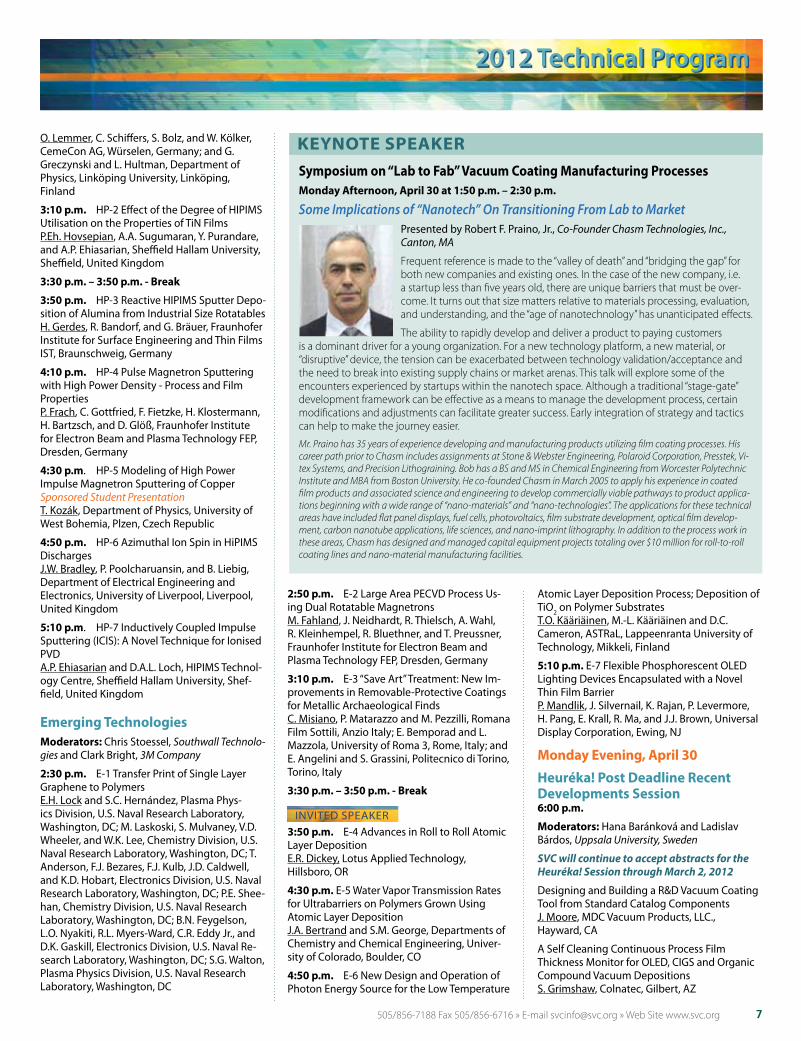
Some implications of “nanotech” On Transitioning From Lab to MarketPresented by Robert Praino, Chasm Technologies, Canton, MA See abstract and biographical sketch on page 7 .
Symposium on “Lab to Fab” Vacuum Coating Manufacturing ProcessesModerator: Carl Lampert, Star Science
2:30 p.m. L2F-1HighThroughputAtomicLayerDepositionofAl2O3forUltrabarrierEncap-sulationofLargeAreaElectronics J.C.S.Kools,EncapsulixSAS,Simiane,France
2:50 p.m. L2F-2 Electrical, Optical Properties of Indium-Tin-Oxide Films Deposited on Poly-ethylene Terephthalate Substrate for Capacitive Touch Panels
D.-H.Kim,TorayAdvancedMaterialsKoreaInc.,Seoul,SouthKorea;J.-Y.Park,TorayAdvancedMaterialsKoreaInc.,Gumi,SouthKorea;andH.-S.JeonandY.-S.Kim,TorayAdvancedMaterialsKoreaInc.,Seoul,SouthKorea
3:10 p.m. L2F-3 Compact Vacuum Web Coat-ing System for R&D H.TamagakiandT.Segawa,KobeSteel,Ltd.,Takasago, Japan3:30 p.m. – 3:50 p.m. - Break
INVITEDSPEAKER Contributed by the Emerging Technologies TAC 3:50 p.m. L2F-4DepositingCopperonFlexiblePolymerswiththeHelpofaNano-Coating A.N.Beavers,Jr., SRIInternational,MenloPark,CA
4:30 p.m. L2F-5InnovativeAutomatedWebInspectionSystems-VisionBeyondDefectDetection in Vacuum Coating Manufacturing Processes J.Koenig, Schenk Vision, Woodbury, MN
INVITEDSPEAKERContributed by the Optical Coating TAC 4:50 p.m. L2F-6RecentAdvancesinMulti-layer Polymeric Interference Reflectors M.F. Weber, 3M Company, St. Paul, MN
Large Area CoatingModerator:MichaelAndreasen,Vacuum Edge
INVITEDSPEAKER
2:30 p.m. L-1AdvancedTransparentContactsforPhotovoltaicandOtherApplications T.M.Barnes,J.Burst,J.L.Blackburn,andT.Gessert, National Renewable Energy Labora-tory, Golden, CO
3:10 p.m. L-2 Recent Developments of TiO2:NbSputteredwithHighDepositionRatesfrom a Rotatable Magnetron System M. Junghähnel and F. Fietzke, Fraunhofer Insti-tuteforElectronBeamandPlasmaTechnologyFEP, Dresden, Germany; and M. Vinnichenko andS.Cornelius,Helmholtz-ZentrumDresden-Rossendorf, Dresden, Germany
3:30 p.m. – 3:50 p.m. - Break
3:50 p.m. L-3ITO97/3CoatingsasTranspar-entContactforHeterojunctionC-SiSolarCells P. LippensandM.Büchel,UMICOREThinFilmsProducts,Balzers,PrincipalityofLiechtenstein;andC.SzepesiandJ.Fargo,UMICOREThinFilmProductsUSA,Providence,RI
4:10 p.m. L-4StructuralandElectricalPropertiesofHighlyTransparentConductiveGa-DopedZnOFilmsbyMagnetronSputtering K.Nagamoto,T.Hara,andT.Kondo,ResearchCenter, LINTEC Corporation, Saitama, Japan; andK.Ishi,UtsunomiyaUniversity,Tochigi,Japan
4:30 p.m. L-5LargeAreaPECVDCoatingsCombined In-Line with Sputtering W. Seaman and J. Madocks, General Plasma, Tucson,Arizona
4:50 p.m. L-6In-LineHot-WireChemicalVaporDepositionofSilicon-BasedCoatings L. Schaefer,T.Harig,M.Hoefer,andA.Laukart,Fraunhofer Institute for Surface Engineering andThinFilmsIST,Braunschweig,Germany;D.BorchertandS.Keipert-Colberg,FraunhoferInstitute for Solar Energy Systems ISE, Gelsen-kirchen, Germany; and J. Trube, Leybold Optics, Alzenau,Germany
5:10 p.m.L-7Plasma-ActivatedElectronBeamPhysical Vapor Deposition - Novel Technologies and Tools G. Mattausch,B.Scheffel,C.Metzner,andF.-H.Roegner,FraunhoferInsituteforElectronBeamand Plasma Technology FEP, Dresden, Germany
High Power impulse Magnetron Sputtering - HiPiMSModerator:RalfBandorf,Fraunhofer Institute for Surface Engineering and Thin Films IST, Germany
INVITEDSPEAKER
2:30 p.m. HP-1HardCoatingsforAdvancedCuttingToolApplicationsProducedbyHiPIMS-Technology
Monday Afternoon, April 3012:50 p.m.– 1:35 p.m.
Emerging Trends in Solid State LightingPresented by Julian Carey, Intematix, Freemont, CA
This talk will focus on the emerging trends in the solid state lighting industry and the growing demand for efficient high quality lighting solutions. Also dis-cussed will be how innovative phosphor and remote phosphor materials are improving LED lighting designs as more manufacturers begin to develop LED lighting solutions to replace incandescent bulbs and fixtures used in general lighting applications. This presentation will include a discussion on lighting system efficacy comparisons between a white LED system and a remote phosphor system using a blue LED to improve light quality. Additionally, this
discussion will highlight how these latest innovations in LED lighting technology have risen to the challenge to make light bulbs, fixtures, TVs and displays brighter and more efficient.
Julian Carey is marketing director at Intematix, a leading innovator of patented phosphors and phosphor compo-nents for high-quality LED lighting. Prior to joining Intematix, Julian directed product management and corporate branding for Prysm, a maker of Laser Phosphor Displays. In the lighting area, Julian was VP of Marketing at LUXIM where he launched plasma lighting products for OEMs in consumer TV, commercial display and general lighting applications. Previously, he served as product marketing manager at Philips Lumileds Lighting where he led the commercialization of their LED product family into diverse markets including cell phone camera flash, printing and imaging, signage and general lighting. Prior to Philips, Julian held product design and process engineering roles developing the first family of power LEDs and systems at the Optoelectronics Division of Hewlett-Packard. He holds a BS degree in mechanical engineering from Stanford University and an MBA from MIT Sloan.
donald M. Mattox Tutorial Program
7505/856-7188 Fax 505/856-6716 » E-mail [email protected] » Web Site www.svc.org
2012 Technical Program
Symposium on “Lab to Fab” Vacuum Coating Manufacturing ProcessesMonday Afternoon, April 30 at 1:50 p.m. – 2:30 p.m.
Some Implications of “Nanotech” On Transitioning From Lab to MarketPresented by Robert F. Praino, Jr., Co-Founder Chasm Technologies, Inc .,
Canton, MA
Frequent reference is made to the “valley of death” and “bridging the gap” for both new companies and existing ones. In the case of the new company, i.e. a startup less than five years old, there are unique barriers that must be over-come. It turns out that size matters relative to materials processing, evaluation, and understanding, and the “age of nanotechnology” has unanticipated effects.
The ability to rapidly develop and deliver a product to paying customers is a dominant driver for a young organization. For a new technology platform, a new material, or “disruptive” device, the tension can be exacerbated between technology validation/acceptance and the need to break into existing supply chains or market arenas. This talk will explore some of the encounters experienced by startups within the nanotech space. Although a traditional “stage-gate” development framework can be effective as a means to manage the development process, certain modifications and adjustments can facilitate greater success. Early integration of strategy and tactics can help to make the journey easier.
Mr. Praino has 35 years of experience developing and manufacturing products utilizing film coating processes. His career path prior to Chasm includes assignments at Stone & Webster Engineering, Polaroid Corporation, Presstek, Vi-tex Systems, and Precision Lithograining. Bob has a BS and MS in Chemical Engineering from Worcester Polytechnic Institute and MBA from Boston University. He co-founded Chasm in March 2005 to apply his experience in coated film products and associated science and engineering to develop commercially viable pathways to product applica-tions beginning with a wide range of “nano-materials” and “nano-technologies”. The applications for these technical areas have included flat panel displays, fuel cells, photovoltaics, film substrate development, optical film develop-ment, carbon nanotube applications, life sciences, and nano-imprint lithography. In addition to the process work in these areas, Chasm has designed and managed capital equipment projects totaling over $10 million for roll-to-roll coating lines and nano-material manufacturing facilities.
KEynOTE SPEAKErO. Lemmer,C.Schiffers,S.Bolz,andW.Kölker,CemeConAG,Würselen,Germany;andG.GreczynskiandL.Hultman,DepartmentofPhysics,LinköpingUniversity,Linköping,Finland
3:10 p.m. HP-2EffectoftheDegreeofHIPIMSUtilisationonthePropertiesofTiNFilms P.Eh.Hovsepian,A.A.Sugumaran,Y.Purandare,andA.P.Ehiasarian,SheffieldHallamUniversity,Sheffield,UnitedKingdom
3:30 p.m. – 3:50 p.m. - Break
3:50 p.m. HP-3ReactiveHIPIMSSputterDepo-sitionofAluminafromIndustrialSizeRotatables H.Gerdes,R.Bandorf,andG.Bräuer,FraunhoferInstitute for Surface Engineering and Thin Films IST,Braunschweig,Germany
4:10 p.m. HP-4PulseMagnetronSputteringwithHighPowerDensity-ProcessandFilmProperties P. Frach,C.Gottfried,F.Fietzke,H.Klostermann,H.Bartzsch,andD.Glöß,FraunhoferInstituteforElectronBeamandPlasmaTechnologyFEP,Dresden, Germany
4:30 p.m. HP-5ModelingofHighPowerImpulse Magnetron Sputtering of Copper Sponsored Student Presentation T.Kozák,DepartmentofPhysics,UniversityofWestBohemia,Plzen,CzechRepublic
4:50 p.m. HP-6AzimuthalIonSpininHiPIMSDischarges J.W.Bradley,P.Poolcharuansin,andB.Liebig,Department of Electrical Engineering and Electronics,UniversityofLiverpool,Liverpool,UnitedKingdom
5:10 p.m. HP-7InductivelyCoupledImpulseSputtering(ICIS):ANovelTechniqueforIonisedPVD A.P.EhiasarianandD.A.L.Loch,HIPIMSTechnol-ogyCentre,SheffieldHallamUniversity,Shef-field,UnitedKingdom
Emerging TechnologiesModerators: Chris Stoessel, Southwall Technolo-gies andClarkBright,3M Company
2:30 p.m. E-1 Transfer Print of Single Layer Graphene to Polymers E.H.LockandS.C.Hernández,PlasmaPhys-icsDivision,U.S.NavalResearchLaboratory,Washington, DC; M. Laskoski, S. Mulvaney, V.D. Wheeler,andW.K.Lee,ChemistryDivision,U.S.Naval Research Laboratory, Washington, DC; T. Anderson,F.J.Bezares,F.J.Kulb,J.D.Caldwell,andK.D.Hobart,ElectronicsDivision,U.S.NavalResearch Laboratory, Washington, DC; P.E. Shee-han,ChemistryDivision,U.S.NavalResearchLaboratory,Washington,DC;B.N.Feygelson,L.O. Nyakiti, R.L. Myers-Ward, C.R. Eddy Jr., and D.K.Gaskill,ElectronicsDivision,U.S.NavalRe-search Laboratory, Washington, DC; S.G. Walton, PlasmaPhysicsDivision,U.S.NavalResearchLaboratory, Washington, DC
2:50 p.m. E-2LargeAreaPECVDProcessUs-ing Dual Rotatable Magnetrons M. Fahland,J.Neidhardt,R.Thielsch,A.Wahl,R.Kleinhempel,R.Bluethner,andT.Preussner,FraunhoferInstituteforElectronBeamandPlasma Technology FEP, Dresden, Germany
3:10 p.m. E-3“SaveArt”Treatment:NewIm-provements in Removable-Protective Coatings forMetallicArchaeologicalFinds C. Misiano, P. Matarazzo and M. Pezzilli, Romana FilmSottili,AnzioItaly;E.BemporadandL.Mazzola,UniversityofRoma3,Rome,Italy;andE.AngeliniandS.Grassini,PolitecnicodiTorino,Torino, Italy
3:30 p.m. – 3:50 p.m. - Break
INVITEDSPEAKER3:50 p.m. E-4AdvancesinRolltoRollAtomicLayer Deposition E.R. Dickey,LotusAppliedTechnology,Hillsboro,OR
4:30 p.m. E-5 Water Vapor Transmission Rates forUltrabarriersonPolymersGrownUsingAtomicLayerDeposition J.A.Bertrand and S.M. George, Departments of ChemistryandChemicalEngineering,Univer-sityofColorado,Boulder,CO
4:50 p.m. E-6 New Design and Operation of Photon Energy Source for the Low Temperature
AtomicLayerDepositionProcess;DepositionofTiO2 on Polymer Substrates T.O.Kääriäinen,M.-L.KääriäinenandD.C.Cameron,ASTRaL,LappeenrantaUniversityofTechnology, Mikkeli, Finland
5:10 p.m. E-7 Flexible Phosphorescent OLED Lighting Devices Encapsulated with a Novel ThinFilmBarrier P. Mandlik,J.Silvernail,K.Rajan,P.Levermore,H.Pang,E.Krall,R.Ma,andJ.J.Brown,UniversalDisplay Corporation, Ewing, NJ
Monday Evening, April 30Heuréka! Post deadline recent developments Session 6:00 p.m.
Moderators:HanaBaránkováandLadislavBárdos,Uppsala University, Sweden
SVC will continue to accept abstracts for the Heuréka! Session through March 2, 2012
DesigningandBuildingaR&DVacuumCoatingTool from Standard Catalog Components J. Moore, MDC Vacuum Products, LLC., Hayward,CA
ASelfCleaningContinuousProcessFilmThickness Monitor for OLED, CIGS and Organic Compound Vacuum Depositions S. Grimshaw,Colnatec,Gilbert,AZ

Society of Vacuum Coaters » 2012 TechCon Preliminary Program 8
2012 Technical Program
Tuesday Morning, May 1Technology Forum Breakfast7:00 a.m. – 8:15 a.m.
Facilitator-led round table discussions provide an opportunity for information, conversation and interaction on specific subjects. See this page for topics and facilitators .
Symposium on New Materials and Pro-cesses for Photovoltaics ManufacturingModerator: Tim Gessert, National Renewable Energy Laboratory (NREL)
INVITEDSPEAKER
Contributed by the Coatings for Cleantech Energy Conversion, Storage and Related Processes TAC 8:30 a.m. PV-8 Mass Production of Photovol-taic Modules: Low Cost Fabrication, Perfor-mance and Potential W.S. Sampath, Department of Mechanical Engineering,ColoradoStateUniversity,Ft.Col-lins, CO
9:10 a.m. PV-9 Influence of Substrate Tem-peratureandActivationTreatmentonCdTeSolar Cells H.Morgner,K.Haefner,O.Zywitzki,T.Modes,and C. Metzner, Fraunhofer Institute for Electron BeamandPlasmaTechnologyFEP,Dresden,Germany;andB.SiepchenandC.Drost,Roth&RauAG,Hohenstein-Ernstthal,Germany
INVITEDSPEAKERContributed by the Optical Coating TAC 9:30 a.m. PV-10ChallengesandOpportuni-ties of Emerging PV Technologies
J.A.Zapien,CityUniversityHongKong,Kow-loon,HongKong
10:10 a.m. – 10:30 a.m. - Break
Symposium on “Lab to Fab” Vacuum Coating Manufacturing ProcessesModerator: Susan Murray, Custom ASIC
INVITEDSPEAKERContributed by the Emerging Technologies TAC 10:30 a.m. L2F-7 From Lab to Fab - Training Technicians for an Innovation Economy R.D. Cormia,FoothillCollege,LosAltosHills,CA
11:10 a.m. L2F-8 Study of the Deposition of Mixed Cerium Oxide Thin Films by Reactive Magnetron Sputtering for the Development of Corrosion Protective Coatings Sponsored Student Presentation S. Ershov, Chimie des Interactions Plasma Surfaces,UniversityofMons,Mons,Belgium;M.-E. Druart, Department of Materials Science, UniversityofMons,Mons,Belgium;D.Music,MaterialsChemistry,RWTHAachenUniversity,Aachen,Germany;M.-G.Olivier,DepartmentofMaterialsScience,UniversityofMons,Mons,BelgiumandMateriaNovaResearchCenter,Mons,Belgium;andR.Snyders,ChimiedesIn-teractionsPlasmaSurfaces,UniversityofMons,Mons,BelgiumandMateriaNovaResearchCenter,Mons,Belgium
11:30 a.m. L2F-9AutomaticProcessControlofDeposition Processes; Present State and Future Direction J.McKim,NVisionInstruments,SantaCruz,CA
11:50 a.m. L2F-10ClosedLoopProcessControlforReactiveDCSputteringZn:AltoCreateTransparent Conductive Oxide (TCO) Films M.A.BernickandR.Newcomb,AngstromSci-ences,Inc.,Duquesne,PA
Business TopicsModerator: FrankZimone,Angstrom Sciences
INVITEDSPEAKER8:30 a.m. BT-1SellinghasNothingtodowithSelling R.P. Farrell,TangentKnowledgeSystems, Chicago, IL
9:10 a.m. BT-2Real-Win-Worth,aValuableTool for Reducing Risks when Introducing In-novative Products D.J. McClure,AcuityConsultingandTraining,Siren, WI
Joint Session: Plasma Processing/HiPiMSModerator: Mariadriana Creatore, Eindhoven University of Technology, The Netherlands
9:30 a.m. P-9 New Method Of Generation HighPowerPulseMagnetronDischarge(HIP-IMS/MPP)BasedonOscillatoryVoltageWaveForms R. ChistyakovandB.Abraham,ZondInc/ZpulserLLCMansfield,MA;andJ.Y.ParkandJ.G.Park,SEMICATInc,Fremont,CA
Topics and FacilitatorsTuesday, May17:00 a.m. – 8:15 a.m.
Atmospheric Plasma Technologies – HanaBaránkováandLadislavBárdos,Uppsala University, Sweden
Cleantech Energy Conversion and Stor-age – Carl Lampert, Star Science and Ric Shimshock, MLD Technologies, LLC
diamond-Like Carbon (dLC) Coatings –KlausBewilogua,Fraunhofer Institute for Surface Engineering and Thin Films IST, Germany,GerryvanderKolk,IonBond Netherlands b .v ., Venlo, The Netherlands, and LarsHaubold,Fraunhofer, USA
Fabrication and Performance of Optical Coatings – Ludvik Martinu, École Poly-technique de Montréal, Canada, and BryantHichwa,Sonoma State University
Gas/Moisture Permeation Barrier Layers - Mariadriana Creatore, Eindhoven University of Technology, The Netherlands
Magnetron Sputtering – David Glocker, Isoflux Incorporated
Technology Forum Breakfast
Tuesday at a Glance
M O r n i n GTechnical Sessions •SymposiumonNewMaterialsandProcessesfor Photovoltaics Manufacturing •Symposiumon“LabtoFab”VacuumCoating Manufacturing Processes • BusinessTopics •JointSession:PlasmaProcessing/HIPIMS •PlasmaProcessing •TribologicalandDecorativeCoating •EmergingTechnologies •LargeAreaCoatingSpecial Events •5KFunRunandWalk6:00a.m. •TechnologyForumBreakfast7:00a.m.–8:15a.m.Education Program •Sputter Deposition in Manufacturing (Full Day) •Nanostructures:StrategiesforSelf-Organized Growth(AM) •PracticeandApplicationsofHighPowerImpulse MagnetronSputtering(HIPIMS)(AM) •IntroductiontoEllipsometry(AM)
A F T E r n O O nTechnical Sessions •ExecutiveForum12:30p.m. •PlasmaProcessing •PosterSession3:30p.m.–6:00p.m.Special Events •“MeettheExperts”Corner1:15p.m.–2:15p.m. •BusTransportationtoSantanaRow (Starting at 6:15 p.m.)Exhibit •Exhibit12:00p.m.–6:00p.m. •ExhibitCashLunchand“Beerposium” 12:00p.m.–1:30p.m. •ReceptioninExhibitHall4:45p.m.–6:00p.m.Education Program •IntroductiontoPlasmaProcessing Technology (PM) •PropertiesandApplicationsofTribological Coatings (PM) •ManufactureofPrecisionEvaporative Coatings (PM)
9505/856-7188 Fax 505/856-6716 » E-mail [email protected] » Web Site www.svc.org
2012 Technical Program
9:50 a.m. P-10DischargeBehaviorandDepositionofDLCFilminHighPowerPulsedMagnetron Discharge Configuration X. Tian,Z.Wu,G.Gui,C.Gong,andS.Yang,StateKeyLaboratoryofAdvancedWeldingandJoining,HarbinInstituteofTechnology,Harbin,China;andP.K.Chu,DepartmentofPhysicsandMaterialsScience,CityUniversityofHongKong,HongKong,China
10:10 a.m. – 10:30 a.m. – Break
Plasma Processing10:30 a.m. P-11 2-D Spatial Maps of Negative IonDensitiesandTemperaturesinOxygen/Ar-gon Magnetron Plasmas Sponsored Student Presentation S.C. ScribbinsandJ.W.Bradley,DepartmentofElectricalEngineeringandElectronics,Univer-sityofLiverpool,Liverpool,UnitedKingdom
10:50 a.m. P-12 Complex Characterization of GlidingArcDischargeforAdvanceOxidationProcesses P. Spatenka,DepartmentofAppliedPhysicsandTechnology,UniversityofSouthBohemia,CeskéBudejovice,CzechRepublic,DepartmentofMaterialScience,TechnicalUniversityofLi-berec, Liberec, Czech Republic and SurfaceTreat Inc.,Turnov,CzechRepublic;P.Kríz,DepartmentofAppliedPhysicsandTechnology,UniversityofSouthBohemia,CeskéBudejovice,CzechRepublic; J. Cerman, Department of Material Science,TechnicalUniversityofLiberec,Liberec,Czech Republic and SurfaceTreat Inc., Turnov, CzechRepublic;J.Sláma,CzechTechnicalUniversityinPrague,Praha,CzechRepublic;P.Barto,DepartmentofAppliedPhysicsandTechnology,UniversityofSouthBohemia,CeskéBudejovice,CzechRepublic;andJ.Píchal,CzechTechnicalUniversityinPrague,Praha,Czech Republic
INVITEDSPEAKER11:10 a.m. P-13 The Multiple Resonance Probe: ANovelDeviceforIndustryCompatiblePlasmaDiagnostics R.P.Brinkmann, Theoretical Electrical Engi-neering,RuhrUniversityBochum,Bochum,Germany
11:50 a.m.P-14FrequencyProbeMeasure-ments of Electron Density, Plasma Potential, and Electron Energy Distribution in Processing Plasmas D.R.Boris, S.G. Walton, and R.F. Fernsler, Plasma PhysicsDivision,U.S.NavalResearchLabora-tory, Washington, DC
Tribological and decorative CoatingModerators:PapkenHovsepian,Sheffield Hal-lam University, United Kingdom and Christoph Leyens, Technische Universität Dresden, Germany
8:30 a.m. T-8EngineeringtheDLCCoating/Lubricant Interface: Optimization for Effective
Friction and Wear Reduction A.Neville,A.Morina,L.Austin,andT. Liskiewicz, SchoolofMechanicalEngineering,UniversityofLeeds,UnitedKingdom;andR.Tietema,HauzerTechnoCoatingBV,Venlo,TheNetherlands
8:50 a.m. T-9HowContaminantsAffecttheQualityofPVDCoatingsandtheirAffectonProcess Parameters Z.WangandM.Akkaoui,TanuryIndustries,Lincoln, RI
INVITEDSPEAKER9:10 a.m. T-10NanostructuredCarbonandTiNBasedCoatingsDepositedbyFilteredVacuum-ArcApparatusinNSCKIPT,Ukraine I.I.Aksenov,V.A.Belous,andV.E.Strel’nitskij, NationalScienceCenter,KharkovInstituteofPhysicsandTechnology,Kharkov,Ukraine
9:50 a.m. T-11 Multicomponent Deposition by a Magnetron with a Non-Equipotential Cathode V.V.Zhurin,ColoradoAdvancedTechnologyLLC,FortCollins,CO;andP.A.TsygankovandN.G.Elistratov,BaumanStateTechnicalUniver-sity, Moscow, Russian Federation
10:10 a.m. – 10:30 a.m. – Break
10:30 a.m.T-12PulsedLaserAblationofRepa-rableErosion-ResistantCoatingsforAerospace Sponsored Student Presentation A.Ragusich,J.E.Klemberg-Sapieha,andL.Martinu,ÉcolePolytechniquedeMontréal,Montréal,Canada 10:50 a.m. T-13 Tuning Colors In Protective Metal Nitride Coatings by the Control of Absorption/InterferenceEffects M. Panjan, Jozef Stefan Institute, Ljubljana, SloveniaandÉcolePolytechniquedeMontréal,Montréal,Canada;M.CekadaandP.Panjan,Jozef Stefan Institute, Ljubljana, Slovenia; M. KlanjsekGunde,NationalInstituteofChem-istry, Ljubljana, Slovenia; and R. Vernhes and L.Martinu,ÉcolePolytechniquedeMontréal,Montréal,Canada
11:10 a.m. T-14TribologicalBehaviourofHeatTreated Tungsten Doped Diamond-Like Carbon CoatingatHighTemperatures
Sponsored Student Presentation A.AbouGharam,MechanicalAutomotiveandMaterialsDepartment,UniversityofWindsor,Windsor, Canada; M.J. Lukitsch, Materials and Processes Laboratory, General Motors R&D Center,Warren,MI;andA.T.Alpas,MechanicalAutomotiveandMaterialsDepartment,Univer-sity of Windsor, Windsor, Canada
11:30 a.m.T-15CorrosionBehaviorofDuplexPVD Coatings in Comparison to Duplex Coat-ingsBasedonElectroplatedBaseCoatingsandPVD Top Coatings M.V.Ravichandran,IonbondUSA,Green-borough, NC; F. Derangere, Ionbond France, Paris,France;andT.Hurkmans,IonbondUSA,MadisonHeights,MI
11:50 a.m. T-16 Optimisation of Coating MechanicalPropertiesbySimulationBasedonExperimental Data B.Zhou,N. Randall,andD.Griffin,CSMInstru-ments,Needham,MA
Emerging TechnologiesModerators: Chris Stoessel, Southwall Technologies andClarkBright,3M Company
INVITEDSPEAKER8:30 a.m. E-8Metalcones:HybridOrganic-InorganicFilmsFabricatedUsingAtomicandMolecular Layer Deposition Techniques S.M. George,B.Lee,B.Yoon,A.I.Abdulagatov,andR.A.Hall,DepartmentsofChemistryandChemicalEngineering,UniversityofColorado,Boulder,CO
9:10 a.m. E-9 Functional Nanoparticle Coatings A.H.Kean,S.Saranu,V.Broadley,G.VatougiaandL.Allers,MantisDepositionLtd.,Thame,UnitedKingdom
9:30 a.m. E-10VacuumDepositionofConju-gated Polymers for Organic Photovoltaics Sponsored Student Presentation P.Kovacik,H.E.AssenderandA.A.R.Watt,DepartmentofMaterials,UniversityofOxford,Oxford,UnitedKingdom
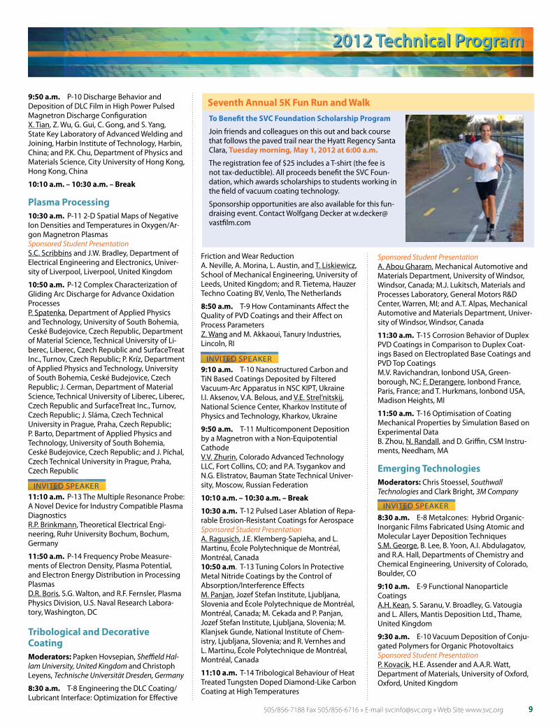
To Benefit the SVC Foundation Scholarship Program
Join friends and colleagues on this out and back course thatfollowsthepavedtrailneartheHyattRegencySantaClara, Tuesday morning, May 1, 2012 at 6:00 a.m.
Theregistrationfeeof$25includesaT-shirt(thefeeisnottax-deductible).AllproceedsbenefittheSVCFoun-dation, which awards scholarships to students working in the field of vacuum coating technology.
Sponsorship opportunities are also available for this fun-draising event. Contact Wolfgang Decker at [email protected]
Seventh Annual 5K Fun run and Walk

Society of Vacuum Coaters » 2012 TechCon Preliminary Program 10
2012 Technical Program
Tuesday Afternoon, May 1
SVC Exhibit Cash Lunch and “Beerposium” – it’s 5 o’clock somewhere12:00 p.m. – 1:30 p.m.
“Meet the Experts” Corner1:15 p.m. – 2:15 p.m.
Tim Gessert, National Renewable Energy Laboratory Topic: Polycrystalline Thin-Film Photovoltaics
Executive Forum: road Mapping of Future Thin Film Products12:30 p.m. – 1:30 p.m.
Forum Moderators: Carl Lampert, Star Science and Paula Mints, Navigant
Co-Organizers:MichaelAndreasen,Vacuum Edge, and Ric Shimshock, MLD Technologies LLC
Forum Speakers: Michael Lebby, General Manager and Chief TechnologyOfficer,TranslucentInc., PaloAlto,CA “Driving‘On-Silicon’SolutionsinLEDLighting,PowerElectronics,andSolarCPVCellsUsingGaN-on-Si and Ge-on-Si Large Format Silicon Wafers” BettinaWeiss,ExecutiveDirector,PVGroup,SEMI,SanJose,CA “WhataDifferenceaYearMakes–TheGlobalPVIndustry in a Changing Global Environment”
Plasma ProcessingModerator:DavidBoris,U .S . Naval Research Laboratory
INVITEDSPEAKER1:30 p.m. P-15 Plasma Processing System DesignUsingPlasmaandElectromagneticModeling S. Rauf,J.Kenney,A.Agarwal,K.Bera,A.Balakrishna,andK.Collins,AppliedMaterials,Inc.,Sunnyvale,CA
2:10 p.m. P-16 3D Numerical Study of Differ-ent Magnet Systems to Reduce Cross Corner Effect in Rectangular Magnetron Sputtering K.Lacis, Sidrabe Inc., Riga, Latvia; M. Sarma, UniversityofLatvia,Riga,Latvia;andM.Mishels-PiesinsandV.Kozlovs,SidrabeInc.,Riga,Latvia
2:30 p.m. P-17 Plasma Generation by Induc-tiveCouplingwithaResonantPlanarAntenna P. Guittienne,Helyssen,Belmont-sur-Lausanne,Switzerland; P. Fayet, TetraPack, Romont, Switzerland;andS.Lecoultre,A.Holling,andC.Hollenstein,ÉcolePolytechniqueFederaledeLausanne (EPFL), Lausanne, Switzerland
2:50 p.m. P-18HydrogenatedDiamond-LikeCarbonDepositionbyUsinganAnodeLayerType Linear Ion Source J.-K.KimandS.Lee,KoreaInstituteofMaterialsScience,Changwon,Korea;K.-H.NamandT.-Y.Kim,POSCOTechnologyResearchLaboratory,Gwangyang-si,Korea;andD.-G.Kim,KoreaInsti-tuteofMaterialsScience,Changwon,Korea
3:10 p.m. P-19 Self Contained Plasma Source for Remote and Projected Plasma Generation D. Carter,D.Hoffman,R.Grilley,andK.Peterson,AdvancedEnergyIndustriesInc.,FortCollins,CO
3:30 p.m. P-20InVacuumPlasmaCleaningSources of Non-Electrically Conductive Sub-strates
D.Monaghan,R.Brown,V.Bellido-Gonzalez, andM.Audronis,GencoaLtd,Liverpool,UnitedKingdom;andS.Williams,GencoaUSA,SanFrancisco,CA
Poster Presentations3:30 p.m. – 6:00 p.m. in the Exhibit Hall
SVC will continue to accept abstracts for the Poster Session through March 2, 2012 for publication in the Final Program
Poster-1Nano-StructuredAmphiphilicPlasmaPolymersforTuningtheAdhesionofCells I. Gordeev,D.Arzhakov,P.Solar,A.Serov,A.Artemenko,andO.Polonskyi,FacultyofMathematicsandPhysics,CharlesUniversityin Prague, Prague, Czech Republic; J. Ponti, InstituteforHealthandConsumerProtection,European Commission, Joint Research Centre, Ispra,Italy;J.Kousal,O.Kylian,A.Choukou-rov,D.SlavinskaandH.Biederman,FacultyofMathematicsandPhysics,CharlesUniversityinPrague, Prague, Czech Republic
Poster-4 Cylindrical Magnetrons Sputter Depo-sition of Ti-Si-C-N Nanocomposite Coatings on Inner Surface of Cylinders R. Wei and E. Langa, Southwest Research Insti-tute,SanAntonio,TX
Poster-5 Choosing the Right Flow Meter for YourApplication N. Glover,BrooksInstrument,LLC,Snellville,GA
Poster-6 Reduction of Particle Contamina-tionbyHandlingandPlasmaPretreatmentforDefect Sensitive Coatings R.BandorfandG.Bräuer,FraunhoferInstitutefor Surface Engineering and Thin Films IST, Braunschweig,Germany
Poster-7 Deposition of Piezoresistive Films for StrainGaugeApplicationUsinganIndustrialHigh-RateIn-LineSputteringSystem R.Bandorf, Fraunhofer Institute for Surface EngineeringandThinFilmsIST,Braunschweig,Germany; M. Petersen, Institut für Oberflächen-technik,TechnischeUniversitätBraunschweig,Braunschweig,Germany;andU.Heckmann,andG.Bräuer,FraunhoferInstituteforSurfaceEngineeringandThinFilmsIST,Braunschweig,Germany
Poster-8AccurateReflectanceandTransmit-tance Measurements for Optical Coatings R.R. Willey, Willey Optical, Consultants, Charle-voix, MI
Poster-9 Hall-CurrentIonSourcesBasicParam-eters Improvement and Expansion V.V.Zhurin,ColoradoAdvancedTechnologyLLC,FortCollins,CO;andM.Choi,VAC-TECCo.,Kyonggi-Do,Korea
Poster-10 PlasmaAssistedReactiveMagnetronSputtering of Demanding Interference Filters
9:50 a.m.E-11SynthesisofSolar-ActivatedMaterials for the Controlled Release of Volatile Compounds C.J. Tavares, L.F. Oliveira, and J.F. Marques, Cen-treofPhysics,UniversityofMinho,Guimaraes,Portugal; and P. Parpot, Centre of Chemistry, UniversityofMinho,Braga,Portugal
10:10 a.m. – 10:30 a.m. – Break
Large Area CoatingModerator: Johannes Strümpfel, VON AR-DENNE, Germany
10:30 a.m. L-8HardwareandTechnologyforModern Glass Coating C.Koeckert,VONARDENNEAnlagentechnikGmbH,Dresden,Germany
10:50 a.m. L-9 Solid State Laser Inspection of LargeAreaCoatings T. Potts, Dark Field Technologies, Inc., Orange, CT
11:10 a.m L-10CharacterizationofOrganicLight Emitting Diode Devices by Spectroscopic Ellipsometry K.UppireddiandL.Yan,HoribaScientific,Edison, NJ
11:30 a.m.L-11AdvancesinPowerSuppliesforHighArcRateApplications D.J. Christie,S.Kovacevic,F.G.Tomasel,andH.Walde,AdvancedEnergyIndustries,Inc.,FortCollins, CO
11:50 a.m. L-12 Next Generation of Mid- FrequencyPowerSuppliesforPlasmaApplica-tions P. Wiedemuth,R.Merte,andU.Richter, HÜTTINGERElektronikGmbH,Freiburg, Germany
SVC Exhibit Opens! 12:00 p.m. – 6:00 p.m.
Don’t Miss the Only Exhibit Dedicated to Vacuum Coating Technologies

11505/856-7188 Fax 505/856-6716 » E-mail [email protected] » Web Site www.svc.org
2012 Technical Program
H.Hagedorn, W. Lehnert, J. Pistner, M. Scherer, andA.Zöller,LeyboldOptics,Alzenau,Germany
Poster-11 Magnetron Sputtering System for SmallBatchHighThroughputProduction D.R. GibsonandJ.L.Martin,AppliedMultilayersLLC,Cheyenne,WY;F.Placido,ThinFilmCentre,UniversityoftheWestofScotland,Paisley,UnitedKingdomandScottishUniversitiesPhys-icsAlliance(SUPA)
Poster-12 Computational Optimization of the HomogeneityofMagnetron-SputteredPreci-sion Optical Filters by Means of Particle in Cell Plasma Simulations – Comparison of Theory with Experiments M. Vergöhl,A.Pflug,D.Rademacher,andT.Zickenrott,FraunhoferInstituteforSurfaceEngineeringandThinFilmsIST,Braunschweig,Germany
Poster-13MetalSurfaceModificationUsingSurface Texturing and Coatings D.-G.Kim,S.Lee,andJ.-K.Kim,KoreaInstituteofMaterialsScience,Changwon,Korea
Poster-14 The Composition Dependent MechanicalPropertyandTribologicalBehaviorof Sputtered Ternary Chromium-Molybdenum-Nitride Films Y.Zou,UniversityofAlabamaatBirmingham,Birmingham,AL;M.J.Walock,UniversityofAlabamaatBirmingham,Birmingham,ALandLaboratoireBourguignondesMatériauxetProcédés,CERArtsetMétiersParisTechofClu-ny, Cluny, France; I. Rahil and C. Nouveau, Labo-ratoireBourguignondesMatériauxetProcédés,CERArtsetMétiersParisTechofCluny,Cluny,France;andA.Stanishevsky,UniversityofAla-bamaatBirmingham,Birmingham,AL
Poster-15StudyoftheRelationshipBetweenaGas-BarrierPropertyandtheMembraneStressof Films Made by a Cat-CVD Method T. Tsutsumi,H.Yanagihara,H.Amanai,andS.Yoshida,MitsubishiPlastics,Inc.,Shiga,Japan;andY.Watanabe,K.Ohdaira,andH.Matsumura,AdvancedInstituteofScienceandTechnology(JAIST),Ishikawa,Japan
Poster-16ANovelPVDMethodforHighRateandLargeAreaCoatings K.H.Nam,T.Y.Kim,Y.J.Kwak,D.Y.Lee,M.J.Eom,Y.H.Jung,W.S.JungandS.J.Hong,POSCOTech-nicalResearchLab,Gwangyang-si,SouthKorea
Poster-17BatchandContinuousZincCoatingby EML PVD Process W.-S. Jung,D.-Y.Lee,K.-H.Nam,M.-J.Eom,S.-J.Hong,T.-Y.Kim,Y.-J.Kwak,andY.-H.Jung,Technical Research Laboratories, POSCO, Gwangyang-si,Korea
Poster-18 Process Development for Sputtering ofp-TypeConductingCu-Al-OMixtures C. Schulz,C.BalmerandB.Szyszka,FraunhoferInstitute for Surface Engineering and Thin Films IST,Braunschweig,Germany
Poster-19 Preparation and Characterization of Structures Composed of Silver and Copper Thin Films Thermal Evaporated on Forcespun Nylon 6 Nanofibers T. Shimizu,Y.Rane,K.Lozano,andD.Mihut,UniversityofTexasPanAmerican,Edinburg,TX
Poster-20AutoresonantIonTrapMonitoringand Control of Sputter Coated Processes T. Swinney,BrooksAutomation,Granville-Phil-lips Products, Longmont, CO
Poster-21ProgressinHIPIMSTechnology–DevelopmentTrendsandApplication’sOp-portunities W. Glazek,A.Klimczak,P.Ozimek,andP.Rozan-ski,HUETTINGERElectronicSp.zo.o.,Zielonka,Poland
Poster-22 Comparative Plasma Enhanced PVD Deposited Ta and CrN for Wear-Erosion-Corro-sion Mitigation Compared to Electrochemical HCCrCoatings S.L. Lee,M.Cipollo,andF.Yee,U.S.ArmyARDEC-BenétLabs,Watervliet,NY;R.Wei,SouthwestResearchInstitute,SanAntonio,TX; J. Lin, W. Sproul, and J.J. Moore, Colorado School of Mines, Golden, CO
Wednesday Morning, May 2Tribological and decorative CoatingModerators: Tomasz Liskiewicz, University of Leeds, United Kingdom and GerryvanderKolk,IonBond Netherlands BV, The Netherlands
8:30 a.m. T-17 Diamond-Like Carbon Films –PreparationTechniques,PropertiesandAp-plications 40 min . Presentation K.BewiloguaandH.-J.Scheibe,FraunhoferInstitute for Surface Engineering and Thin Films IST,Braunschweig,Germany
9:10 a.m. T-18HighPerformanceMicrowavePlasma Source for Industrial Plasma Surface Processing S.Ulrich,J.Ye,M.Stüber,andH.Leiste,Karl-sruheInstituteofTechnology(KIT),Eggenstein-Leopoldshafen, Germany; and R. Tietema
Exhibit receptionAll TechCon Conference registrants and Exhibitors receive a Complimentary drink Ticket4:45 p.m. – 6:00 p.m.
Complimentary Bus Transportation to and from Santana row Shopping and dining district in San JoséFirst departure – 6:15 p.m.
Wednesday, May 2, 2012 8:30 a.m. – 11:30 a.m. Cost is $40.00
YourVacuumWizardis Don McClure, Acuity Consulting and Training
This half-day event is based on an exten-sive set of engaging tabletop demonstra-tions. Many of the
demonstrations use a transparent vacuum chamber, so attendees can “see” the principles of vacuum coating in action. The goals of this event are to make selected concepts related to vacuum and vacuum coating seen and remembered. This in turn provides a path to deeper understanding. Attendeeswillbeofferedhighlyaccessibleand thought provoking demonstrations and/ordescriptionsoftheessentialele-ments and principles of vacuum, vacuum processing and vacuum coating. The pre-sentation is suitable for both non-technical and technical attendees. The only prerequi-site is curiosity about our amazing world.
This presentation provides the attendee with memorable experiences related to: • pressureandvacuum
• vacuumpumps(themanywaysa vacuum wizard produces “good” vacuum levels)
• vacuummeasurementmethods(how vacuum wizards know the vacuum level in a container
• veryhightemperatures(andthemagic of making coatings by evaporation)
• verylowtemperatures(andthemagic of cryopumping)
• howmaterialschangefromsolidto liquid to gas and back (more vacuum coating magic)
• whatthe“meanfreepath”is(andwhy vacuum wizards care)
• whylowpressuresareneededtomake pure coatings (and why the “low” pressures needed can be so different in differentapplications)
There is a small fee of $40 to attend this Special Event.
The number of attendees is limited so that everyone can see the demonstrations. Preregister using the SVC On-line TechCon registration form.
A Wizard’s Guide to understanding Vacuum and Vacuum Coating

Society of Vacuum Coaters » 2012 TechCon Preliminary Program 12
2012 Technical Program
andT.Krug,HauzerTechnoCoatingBV,Venlo,Netherlands
9:30 a.m. T-19TribologicalBehaviorofMetalAlloyedDLCCoatingsinDryandLubricatedConditions M. Evaristo,SEG-CEMUC-DepartmentofMechanicalEngineering,UniversityofCoimbra,Coimbra, Portugal; T. Polcar, National Centre forAdvancedTribology(nCATS),UniversityofSouthampton,Southampton,UnitedKingdom;andA.Cavaleiro,SEG-CEMUC-DepartmentofMechanicalEngineering,UniversityofCoimbra,Coimbra, Portugal
9:50 a.m. T-20EffectoftheSubstrateBiasontheMechanicalPropertiesofBoronCarbide(BC)DepositedUsingtheMediumFrequencyMagnetron Sputtering Technique W.TillmannandF.Hoffmann,InstituteofMateri-alsEngineering,TechnischeUniversitätDort-mund, Dortmund, Germany; and G.Bejarano, Institute of Materials Engineering, Technische UniversitätDortmund,Dortmund,GermanyandDepartmentofMaterialsEngineering,Universi-daddeAntioquia,Medellín,Colombia
10:10 a.m. – 10:30 a.m. – Break
Symposium on New Materials and Pro-cesses for Photovoltaics Manufacturing Moderators:BettinaWeiss,SEMI and Carl Lampert, Star Science
10:30 a.m. PV-11 Deposition of Nb-Doped TiO2FilmsonLargeAreabyCo-SputteringwithPrecise Process Control
F. Fietzke and M. Junghähnel, Fraunhofer Insti-tuteforElectronBeamandPlasmaTechnologyFEP, Dresden, Germany
10:50 a.m. PV-12AStudyofMoO2 Doped SnO2 Transparent and Conductive Thin Films S. SunandP.Kumar,H.C.Starck,Inc.,Newton,MA 11:10 a.m.PV-13HighVacuumSeleniumEvapo-ration for Industrial Production of CIGS Solar Cells D. Gross, S. Stille, and G. Grabosch, Leybold Op-ticsGmbH,Alzenau,Germany;T.HuaultandJ.-L.Guyaux,RiberS.A.,Paris,France
INVITEDSPEAKERContributed by the Coatings for Cleantech Energy Conversion, Storage and Related Processes TAC 11:30 a.m.PV-14AnOverviewoftheMarketforPV Technologies P. Mints,Navigant,PaloAlto,CA
Joint Session: WebTech roll to roll Coatings for High Tech Applications/Large Area CoatingModerators:MichaelAndreasen, Vacuum Edge and John Fahlteich, Fraunhofer Institute for Elec-tron Beam and Plasma Technology FEP, Germany
8:30 a.m. W-1 Roll-to-Roll Manufacturing of Next Generation Display Devices N.A.Morrison,T.Stolley,U.Hermanns,U.Kro-emer,T.Deppisch,H.G.LotzandA.Reus,AppliedMaterialsGmbH&Co.KG,Alzenau,Germany;andD.K.Yim,AppliedMaterials,SantaClara,CA
8:50 a.m. W-2ControlandQuantificationofTexture in Tantalum Sputtering Targets P.Hogan,C.Michaluk,andD.Bozkaya,H.C.Starck,Inc.,Newton,MA
9:10 a.m. W-3 Functional and Decorative Coat-ingsontoMetalStripsDepositedbyPlasma-Acti-
vatedHigh-RateElectronBeamPhysicalVapourDeposition(EBPVD) C. Metzner,B.Scheffel,H.Morgner,andF.Hän-del,FraunhoferInstituteforElectronBeamandPlasma Technology FEP, Dresden, Germany
INVITEDSPEAKER
9:30 a.m. W-4PrintingLow-CostOrganicSolar Cells V. Shrotriya,SolarmerEnergyInc.,ElMonte,CA
10:10 a.m. – 10:30 a.m. – Break
10:30 a.m. W-5 Novel Coatings for Steel Strip via Sputtering Techniques J. Davies, Materials Research Department, SwanseaUniversity,Baglan,UnitedKingdom;and S. Louch, Materials Research Department, SwanseaUniversity,Baglan,UnitedKingdom;and J. Sullivan and C. Weirman, Tata Steel Colors Ltd.,Baglan,UnitedKingdom
10:50 a.m.W-6ITOFilmsonUltra-SlimFlexibleGlass Substrates L. Tian, S. Garner, D. Enicks, P. Sachenik, L. Simp-son,H.Russell,B.Cheney,J.Zhang,J.Lin,C.Kuo,andA.H.Chaturvedi,CorningInc.,Corning,NY
11:10 a.m. W-7 The Role of Plasma Gas Com-positioninOptimizedRoll-to-RollAtomicLayerDepositionofUltraBarrierFilms W.BarrowandE.Dickey,LotusAppliedTechnol-ogy,Hillsboro,OR
11:30 a.m. W-8 Recent Developments in Roll-to-RollALDTechnology T.AlasaarelaandM.Söderlund,BeneqOy,Vantaa, Finland
11:50 a.m. W-9 Interface Investigation of Struc-tures Consisting of Conductive Metallic Thin FilmsDepositedonHighDensityPolyethyleneandStyreneButadieneCopolymerSubstratesReinforced with Vapor Grown Carbon Nanofi-bers for Electromagnetic Interference Shielding Effectiveness Improvement H.Garcia,R.Suarez,D.Mihut,andK.Lozano,Department of Mechanical Engineering, The UniversityofTexasPanAmerican,Edinburg,TX
Optical CoatingModerators: George Dobrowolski, National Research Council of Canada (retired) and Robert Sargent, JDSU
8:30 a.m. O-1 Thin Layers A.Macleod and C. Clark, Thin Film Center Inc., Tuscon,AZ
8:50 a.m. O-2AnalysisofOpticalMonitor-ingStrategiesforNarrowBandpassFiltersbySoftware Simulation R.R. Willey, Willey Optical, Consultants, Charlev-oix,MI;andS.HicksandM.Biagi,IntellemetricsGlobalLtd.,Paisley,UnitedKingdom
9:10 a.m. O-3 Constrained Optimization as a Tool for Choosing Manufacturable Designs A.Tikhonravov and M. Trubetskov, Research ComputingCenter,MoscowStateUniversity;
Wednesday at a Glance
M O r n i n GTAC Breakfast Meetings7:00a.m.–8:15a.m.
Technical Sessions • TribologicalandDecorativeCoating • SymposiumonNewMaterialsandProcessesfor Photovoltaics Manufacturing • JointSession:WebTechRolltoRollCoatingsfor HighTechApplications/LargeAreaCoating • OpticalCoating • CoatingsforCleantechEnergyConversion, Storage and Related Processes • VacuumProcessesandCoatingsforBiomedical Applications
Education ProgramFullDayTutorials8:30a.m.–4:30p.m. • TroubleshootingforThinFilmDeposition Processes • PracticalAspectsofVacuumTechnology:
Operation and Maintenance of Production Vacuum Systems • IonBeamProcessingTechnology • PracticeofReactiveSputtering
Exhibit •ExhibitOpensat10:00a.m.
A F T E r n O O nTechnical Sessions
• DonaldM.MattoxTutorial12:30p.m.–1:10p.m. • OpticalCoating
Special Events •“MeettheExperts”Corner1:15p.m.–2:15p.m. •“MeettheExperts”Corner2:15p.m.–3:15p.m.
Exhibit •Exhibit10:00a.m.–5:00p.m. •BeerBlast3:30p.m.–5:00p.m.
SVC Exhibit Opens!10:00 a.m. – 5:00 p.m.

13505/856-7188 Fax 505/856-6716 » E-mail [email protected] » Web Site www.svc.org
2012 Technical Program
andZ.-S.Wang,InstituteofPrecisionOpticalEngineering,TongjiUniversity,Shanghai,China
9:30 a.m. O-4Spikes C. ClarkandA.Macleod,ThinFilmsCenter,Inc.,Tucson,AZ
9:50 a.m. O-5ModernApproachestoRaisinganAccuracyofBroadbandOpticalMonitoringof Optical Coating Production A.Tikhonravov,M. Trubetskov,andT.Amotchki-na, Research Computing Center, Moscow State University,Moscow,RussianFederation
10:10 a.m. – 10:30 a.m. – Break
Moderators:BenGallagher,Ball Aerospace and Technologies Corp . and Ian Stevenson, Quantum Coating Inc .
10:30 a.m.O-6HardHighIndexNanocompos-iteAl-Si-NCoatingsforOpticalApplications J.E.Klemberg-Sapieha, Department of Engi-neeringPhysics,ÉcolePolytechniquedeMon-tréal,Montréal,Canada;J.Patscheider,EMPA,Dübendorf, Switzerland; and R. Vernhes, M. Azzi,andL.Martinu,DepartmentofEngineer-ingPhysics,ÉcolePolytechniquedeMontréal,Montréal,Canada
10:50 a.m.O-7InvestigationsonAdhesionof Sputtered Layers on Polytetrafluorethylene Surfaces T. Neubert and M. Vergöhl, Fraunhofer Institute for Surface Engineering and Thin Films IST, Braunschweig,Germany
11:10 a.m. O-8 The Majority Carrier Polarity and p-n Junction in Titanium Dioxide Films and their Influence to Photoactivity and Photocata-lytic Properties M.-L.KääriäinenandD.C.Cameron,ASTRaL,LappeenrantaUniversityofTechnology,Mikkeli,Finland
11:30 a.m. O-9 Reversible Water-Induced Stress Evolution in Nanoporous Inorganic SiO2 andHybridSiOCHFilms O.Zabeida,T.Poirié,R.Vernhes,J.E.Klemberg-SapiehaandL.Martinu,ÉcolePolytechniquedeMontréal,Montréal,Canada
11:50 a.m. O-10MixedOxidesforUltravioletCoatings Prepared by Pulsed Reactive Magne-tron Sputtering S.Brunsand M. Vergöhl, Fraunhofer Institute for SurfaceEngineeringandThinFilmsIST,Braun-schweig, Germany
Coatings for Cleantech Energy Conversion, Storage and related ProcessesModerators: Claes Granqvist, Uppsala Univer-sity, Sweden and Carl Lampert, Star Science
INVITEDSPEAKER8:30 a.m. CT-1 Cool Roofs: Coatings, Glazings and Structures for Enhanced Thermal Perfor-mance G. Smith,UniversityofTechnology,Sydney,Sydney,Australia
Wednesday Afternoon, May 2“Meet the Experts” Corner1:15 p.m. – 2:15 p.m. David Glocker, Isoflux Incorporated Topic: BiomedicalCoatingsandSurfaceTreat-ments
2:15 p.m. – 3:15 p.m. Dan Carter, Advanced Energy Industries, Inc . Topic: PowerSupplies,Hardware,andAs-sociatedComponentsforEfficientandStablePlasma Generation
The donald M. Mattox Tutorial Program12:30 p.m. – 1:10 p.m. Seepage14fordetails
Optical CoatingModerators:BryantHichwa,Sonoma State University (retired) and JuanAntonioZapien, City University Hong Kong, People’s Republic of China
INVITEDSPEAKER
1:30 p.m. O-11 JWST Mirror Production Status B.Gallagher,M.Bergeland,B.Brown,D.Chaney,
9:10 a.m. CT-2 Structure, Optical Properties andThermalStabilityofTiAlSiN/TiAlSiON/SiO2 AbsorberforSolarSelectiveApplications L. Rebouta and P. Capela, Centre of Physics, UniversityofMinho,Guimarães,Portugal;M.Andritschky,CentreofPhysics,UniversityofMinho,Guimarães,PortugalandSavoSolarOy,Mikkeli,Finland;A.Matilainen,P.Santilli,andK.Pischow,SavoSolarOy,Mikkeli,Finland;andE.Alves,PhysicsDepartment,ITN,Sacavém,Portugal
9:30 a.m. CT-3High-SpeedAtomicLayerChemical Vapor Deposition of Gallium Nitride Thin Films P.N. GadgilandP.J.Dusza,AtomicPrecisionSystemsInc.,SantaClara,CA
9:50 a.m. CT-4NewHighUptimeDirectPlasmaPECVDCoatingEquipmentforSiN:HSolar Cell Passivation G. Mahnke,W.Mischke,J.Krempel-Hesse,andA.Geiss,SchmidVacuumTechnologyGmbH,Karlstein,Germany
10:10 a.m. – 10:30 a.m. – Break
Vacuum Processes and Coatings for Biomedical ApplicationsModerators: David Glocker, Isoflux Incorpo-rated and HanaBaránková,Uppsala University, Sweden
INVITEDSPEAKER10:30 a.m. BIO-1Thin-FilmCoatingsandPlasma Processing for Improving the Fixation ofBoneImplants S.Kumar, Coatings Mantra Science and Tech-nologyConsulting,Greenwith,Australia
11:10 a.m. BIO-2Silver/Copper-MixedLayersObtained by PVD G. Gotzmann and C. Wetzel, Fraunhofer Insti-tuteforElectronBeamandPlasmaTechnol-ogyFEP,Dresden,Germany;L.Achenbach,N.Özkucur,andR.H.Funk,FacultyofMedicine,TechnicalUniversity,Dresden,Germany;andC.Werner, Leibniz-Institute of Polymer Research Dresden e.V., Dresden, Germany
11:30 a.m. BIO-3DLC(H)DopedwithZrCoat-ingsforOrthopaedicsApplications Sponsored Student Presentation A.Escudeiro,SEG-CEMUCDepartmentofMechanicalEngineering,UniversityofCoimbra,Coimbra, Portugal; T. Polcar, School of Engineer-ingSciences,UniversityofSouthampton,South-ampton,UnitedKingdom;andA.Calaveiro,SEG-CEMUCDepartmentofMechanicalEngineering,UniversityofCoimbra,Coimbra,Portugal
11:50 a.m. BIO-4DevelopmentofCutting-Edge Ni-Ti Film Technology for Medical Device Applications D. Xu and S. Carpenter, Palmaz Scientific, Inc., Fremont,CA

Society of Vacuum Coaters » 2012 TechCon Preliminary Program 14
2012 Technical Program
T.Copp,K.Lewis,B.Shogrin,K.Smith,andJ.Sokol,BallAerospaceandTechnologiesCorp.,Boulder,CO;J.Hadaway,UniversityofAlabama,Huntsville,AL;H.Glatzel,P.Johnson,andA.Lee,L-3CommunicationsIOSTinsley,Richmond,CA;D.PatriarcaandI.Stevenson,QuantumCoatingIncorporated, Moorestown, NJ; J. Cluney and T.Parsonage,MaterionBrushBerylliumandComposites,Elmore,OH;J.CalvertandB.Rodg-ers,AXSYSTechnologies,Cullman,AL;A.McKayandS.Texter,NorthropGrummanAerospaceSystems,RedondoBeach,CA;L.Cohen,SAO,Cambridge,MA;andL.Feinberg,NASAGoddardSpace Flight Center, Greenbelt, MD
INVITEDSPEAKER2:10 p.m. O-12 Gold Coatings for the Reflec-tive Optics on James Webb Space Telescope (JWST)
14
Thursday Morning, May 3Coatings for Cleantech Energy Conversion, Storage and related ProcessesModerators: Ric Shimshock, MLD Technologies LLC and Carl Lampert, Star Science
8:30 a.m. CT-5 Superfenestration Combining Electrochromic and Thermochromic Function-alities C.G. Granqvist,TheAngstromLaboratory,Up-psalaUniversity,Uppsala,Sweden
8:50 a.m. CT-6ExploringaNovelFilteredArcSourceforUltra-HighRateDepositionofHighQualityZnO:AlTransparentConductingFilms J.L. Slack,S.H.N.Lim,R.J.Mendelsberg,andA.Anders,LawrenceBerkeleyNationalLaboratory,Berkeley,CA
INVITEDSPEAKER9:10 a.m. CT-7 Metal Oxide Films with Func-tional Properties; From TCO and Thermochro-micstoHydrophobicCoatings I.P. Parkin,D.S.Bhachu,N.Noor,andC.Crick,DepartmentofChemistry,UniversityCollegeLondon,London,UnitedKingdom
9:50 a.m. CT-8 The Effect of Film Thickness on the Electrochromic Performance of Nickel Oxide M. NeevesandF.Placido,ThinFilmCentre,Uni-versityoftheWestofScotland,Paisley,UnitedKingdom
10:10 a.m. – 10:30 a.m. – Break
Symposium on New Materials and Pro-cesses for Photovoltaics ManufacturingModerator: David Sanchez, Materion
10:30 a.m.PV-15MultilayerBarrierCoatingsfor Organic Photovoltaics A.M.Coclite,F.DeLuca,andK.K.Gleason,De-partment of Chemical Engineering, Massachu-settsInstituteofTechnology,Cambridge,MA
10:50 a.m. PV-16 Permeation Rate Measure-mentsofUltra-BarriersUsingCavityRing-DownSpectroscopy D.S. ShacklefordandA.Mahfoud-Familia,Saint-Gobain Innovative Materials, Northborough, MA
11:10 a.m. PV-17 Study of Mechanical and WaterVaporBarrierPerformancesforFlexibleOrganic Solar Cells Protecting Coating F. De Luca,A.M.Coclite,andK.K.Gleason,Mas-sachusetts Institute of Technology, Cambridge, MA;andH.Benmansour,TOTALSAOrganic&HybridPhotovoltaic,R&DDivision,Courbevoie,France
Wednesday Afternoon, May 212:30 p.m. – 1:10 p.m.
Vacuum-Arc Surface Modification and Coating Deposition Methods in KIPT, Ukraine (Historical Review)
PresentedbyVladimirStrel’nitskij,National Science Center, Kharkov Institute of Physics and Technology, Kharkov, Ukraine
This short historical sketch presents the invention of new technology in protective wear-resistant coatings deposition and surface modification by a vacuum-arc method at the Kharkov Institute of Physics and Technology (KIPT), and the development of the work in this direction in the former USSR and in CIS. The experience of the KIPT experts is used by other institutions of Ukraine, Russia and other countries in the creation of new specialized installa-tions for vacuum-arc coating deposition and surface modification. Long-term
researches and developments in KIPT are carried out in the following directions:
- Methods of formation and control of the metal plasma streams generated by the cathode spots of an arc in vacuum and low-pressure gas medium - Processes in interelectrode plasma, methods of discharge ignition and stabilization in technological plasma sources; physics and technology of formation of plasma streams with preselected parameters - The mechanisms underlying processes of formation of the functional coatings from metals, their compounds of type of nitrides, oxides, carbides and their combinations - Research of synthesis of micro- and nanostructured composite and multilayer coatings - Extensive experimental and theoretical research on physics and technology of vacuum-arc synthesis of thin and ultrathin films of diamond-like carbon, with an attainment of commercial use of the diamond-like coatings deposition methods created - Vacuum-arc processes for the surface protection of uranium and other materials of nuclear power from atmospheric and hydride corrosion - Methods of duplex surface ion-plasma treatment of materials (nitriding + deposition, plasma immersion ion implantation + deposition)
Vladimir Evgeniyevich Strel’nitskij is a noted scientist in the field of physics and technology of diamond like carbon (DLC) films synthesis. He graduated from Kharkov State University (Ukraine) in 1970. After military service in the So-viet Army (1970-1972) he worked in the National Science Centre “Kharkov Institute of Physics and Technology” (NSC KIPT) since 1972 until now. He received the Candidate (PhD) and Doctor Science degrees in physics and mathematics from Kharkov State University in 1980 and 2003, respectively. At present Dr. Strel’nitskij acts as the head of the Super-hard Carbon Films Laboratory. He is the author of a series of pioneer works on vacuum arc synthesis of diamond-like carbon films. He is coauthor of the new theoretical model of growth of superhard nanocomposite materials includ-ing DLC. The new setups equipped with filtered vacuum-arc plasma sources for deposition of DLC and composite nanostructured TiN based films were developed and applied in industry under his direction. He is the Laureate of the USSR State Prize for service in physics and technology for 1987. Dr. Strel’nitskij is author and coauthor more than 200 science published works and patents.
donald M. Mattox Tutorial Program
C. Childers, D. Patriarca, G. Sadkin, and I. Steven-son,QuantumCoating,Inc,Moorestown,NJ
INVITEDSPEAKER2:50 p.m. O-13 Optimization of the Manufac-turingStrategiesofHighQualityCoatingsintoa 2-Meter Optics Magnetron Sputtering Deposi-tion Machine
M. Lequime, Institut FRESNEL, Marseille, France
SVC Exhibit Beer Blast!3:30 p.m. – 5:00 p.m.

15505/856-7188 Fax 505/856-6716 » E-mail [email protected] » Web Site www.svc.org
2012 Technical Program
WebTech roll to roll Coatings for High-End ApplicationsModerators: AlbertoArgoitia, JDSU Flex Products Group and Chris Stoessel, Southwall Technologies
INVITEDSPEAKER8:30 a.m. W-10MarketOpportunitiesforR2RThin Film Coating L. Gasman,NanoMarkets,LLC,GlenAllen,VA
9:10 a.m. W-11 The Characteristics of Flexible Indium Tin Oxide (ITO) Electrodes Grown on Polyethylene Terephthalate(PET) Substrates UsingMulti-CathodeRoll-to-RollSputteringSystemforUseinFlexibleDisplayandCapaci-tive Type Touch Panel J. Cho,I.S.Kim,andM.H.Lee,LGHausysInsti-tute,Gyunggi-do,SouthKorea
9:30 a.m. W-12 Transparent Conductive Films withLowResistivityandHighOpticalPropertyon Plastic Substrates for Projected Capacitive Touch Sensors G. Nakamura,N.Tatami,H.Murakami,M.Kohmoto,T.Oya,andS.Yokoyama,toyoboco.,LTD., Shiga, Japan
9:50 a.m. W-13 Deposition of Full Dielectric SolarControlStackonPolymerFilmsUsingaCombinedPVD/PECVDApproach M. Fahland, T. Vogt, J. Fahlteich, and N. Schiller, FraunhoferInstituteforElectronBeamandPlasma Technology FEP, Germany
10:10 a.m. – 10:30 a.m. – Break
10:30 a.m.W-14NewSolarControlCoatingsforAutomotiveApplicationtoAchieveLowTotalSolarTransmittanceTTS<40% R.Kleinhempel,A.Wahl,R.Thielsch,andP.Buettrich,SouthwallEuropeGmbH,Grossroeh-rsdorf, Germany
10:50 a.m.W-15Thin-FilmBarriersforFlexibleOLEDs F.vanAsscheandS.Unnikrishnan,HolstCentre/TNO,Eindhoven,TheNetherlands;P.vandeWeijerandP.Bouten,PhilipsResearchLabo-ratories, Eindhoven, The Netherlands; and T. van Mol,HolstCentre/TNO,Eindhoven,TheNetherlands
11:10 a.m. W-16 Roll-to-Roll Technology on PilotScaleforTransparentUltra-HighMultilayerBarriers J. Fahlteich, Fraunhofer Institute for Electron BeamandPlasmaTechnologyFEP,Dresden,Germany;S.Amberg-SchwabandU.Weber,Fraunhofer Institute for Silicate Research ISC, Wuerzberg,Germany;K.Noller,O.Miesbauer,andE.Kücükpinar,FraunhoferInstituteforPro-cess Engineering and Packaging IVV, Freising, Germany; and N. Schiller, Fraunhofer Institute forElectronBeamandPlasmaTechnologyFEP,Dresden, Germany
11:30 a.m. W-17FunctionalCoatingsBasedonVaporDepositionofTriazineBasedCompounds
S. Jahromi,KnowfortTechnologiesBV,Geleen,The Netherlands
11:50 a.m. W-18ClearHardCoatFilmsviaHybridMulti-Layer(HML)VacuumDeposition J.DiBattista, Darly Custom Technology, Inc., Windsor, CT
Optical CoatingModerators:AngusMacleod, Thin Film Center Inc . and UlrikeSchulz,Fraunhofer Institute for Applied Optics and Precision Engineering IOF, Germany
8:30 a.m. O-14PorousSi3N4 Optical Filters for GasSensingApplication R. Vernhes,J.E.Klemberg-Sapieha,andL.Martinu,ÉcolePolytechniquedeMontréal,Montréal,Canada
8:50 a.m. O-15ManufacturingofHigh-Preci-sionOpticalCoatingsUsingaNovelSputteringSystem D. Rademacher and M. Vergöhl, Fraunhofer Institute for Surface Engineering and Thin Films IST,Braunschweig,Germany
9:10 a.m. O-16NewGenerationofEnd-HallIon Sources with Improved Characteristics V.V.Zhurin,ColoradoAdvancedTechnologyLLC,FortCollins,CO;andE.V.KlyuevandA.I.Sidorov, Ion Sources and Technologies, LLC, Troitsk, Russia
9:30 a.m. O-17HighIonCurrentDensityPlasmaSourceforIonAssistedDepositionOverExtendedAreas D.R. Gibson and E.M. Waddell, Thin Film Solu-tionsLtd,Glasgow,UnitedKingdom;andF.Placido,ThinFilmCentre,UniversityoftheWestofScotland,UnitedKingdomandScottishUniversitiesPhysicsAlliance(SUPA)
9:50 a.m. O-18AdvancedDepositionTechnol-ogyforAstronomicalandSpaceApplications M.L. Fulton,SurfaceOpticsCorp.,SanDiego,CA
10:10 a.m. – 10:30 a.m. – Break
Moderators: Georg Ockenfuss, JDSU and James Hilfiker, J .A . Woollam Co ., Inc
10:30 a.m. O-19 Spectroscopic Ellipsometry BeyondThinFilms
J.A.Zapien,R.He,Y.Foo,C.-H.To,andK.T.Cheung, Center Of Super-Diamond and AdvancedFilms(COSDAF)andDepartmentofPhysicsandMaterialsScience,CityUniversityofHongKong,HongKongSAR,People’sRepublicof China
10:50 a.m. O-20OpticalOropertiesofCuOx-ides and N-Doped Cu Oxides S. SongandF.Placido,ThinFilmCentre,Uni-versityoftheWestofScotland,Paisley,UnitedKingdom
11:10 a.m. O-21 Electrochromic Interference FiltersBasedonWO3 and Composite SiO2/WO3 Films B.Baloukas and L. Martinu, Department of EngineeringPhysics,ÉcolePolytechniquedeMontréal,Montréal,Canada
11:30 a.m. O-22 Design and Development of BroadBandAnti-ReflectionCoatingsonSiliconandGaAsSubstratesforSolarCellApplications K.NarasimhaRao and V. Tamilselvan, Depart-mentofInstrumentationandAppliedPhysics,IndianInstituteofScience,Bengaluru,India;and N. Raghu and M. Sudhakar, Solar Panel Divi-sion,ISROSatelliteCentre,Bangalore,India
11:50 a.m. O-23 Indium-Tin Oxide Thin Films: The Effect of Doping Ration Thickness X.-F.Zhang,G.-L.Zhang,Y.-H.Wang,Z.-Q.Huo,Y.-L.Wang,J.-H.Wu,andY.Yan,BeijingInstituteofAeronauticalMaterials(BIAM),Beijing,China
Thursday Afternoon1:40 p.m. – 6:00 p.m.
Thursday at a Glance
M O r n i n GTechnical Sessions
• CoatingsforCleantechEnergyConversion, Storage and Related Processes • SymposiumonNewMaterialsandProcesses for Photovoltaics Manufacturing •WebTechRolltoRollCoatingsforHighTech Applications • OpticalCoating
Education Program • DiamondLikeCarbonCoatings– fromBasicstoIndustrialRealization(AM) • AtmosphericPlasmaTechnologies(AM) • C-IntroductiontoAtomicLayerDeposition (ALD)(AM)
A F T E r n O O nSpecial Events •GilroyWineTour1:40p.m.–6:00p.m.
The Gilroy Wine TourVisiting two popular vineyards in the Southern Santa Clara ValleyOrganizedbySouthBayToursandEvents
DepartsfromtheHyattRegencySantaClaraHotelat1:45p.m.
For details and to register:
http://www.southbaywinetours.com/ svc_gilroy_tour.html

TechCon Tutorial ScheduleYou do not have to register for the TechCon or be a member of SVC to attend tutorials.Anyone can take advantage of the practical problem-solving tutorials developed by the SVC. Taught by some of the most respected pro-fessionals in the vacuum coating industry, these tutorials cover every aspect of vacuum coating and complement the technical conference sessions and Exhibit. Twenty-six tutorials will be offered, including six new tutorials. Discounted fees are available for full time students.
Saturday, April 28V-204 Vacuum Systems, Materials and Operation (O’Hanlon) C-103 An Introduction to Physical Vapor Deposition (PVD) Processes (Shah) C-311 Thin Film Growth and Microstructure Evolution (Greene) C-332 NEW! Zinc Oxide-Based and Other TCO Alternatives to ITO: Materials, Deposition, Properties and Applications (Bright) Sunday, April 29C-203 Sputter Deposition (Greene) - Day 1 of 2-Day Tutorial C-301 Optical Coating Design (Willey) C-335 (AM) NEW! Understandng Solar Cells (Martin) C-330 (PM) Introduction to Thin Film Photovoltaic Technologies (Sittinger & Schlatmann) C-323 High Power Impulse Magnetron Sputtering (Ehiasarian & Anders) Monday, April 30C-211 Sputter Deposition onto Flexible Substrates (McClure) C-322 Characterization of Thin Films (Christensen) C-302 Practical Aspects of Optical Coatings (Morton) C-203 Sputter Deposition (Greene) - Day 2 of 2-Day Tutorial Tuesday, May 1C-210 (PM) Introduction to Plasma Processing Technology (Baránková & Bárdos) . C-318 (AM) Nanostructures: Strategies for Self-Organized Growth (Greene) C-208 Sputter Deposition in Manufacturing (Glocker) C-333 (AM) NEW! Practice and Applications of High Power Impulse Magnetron Sputtering (HIPIMS) (Bandorf & Ehiasarian) M-102 (AM) NEW! Introduction to Ellipsometry (Hilfiker) C-328 (PM) Properties and Applications of Tribological Coatings (Matthews) C-326 (PM) Manufacture of Precision Evaporative Coatings (Oliver) Wednesday, May 2C-212 Troubleshooting for Thin Film Deposition Processes (Ash) V-207 Practical Aspects of Vacuum Technology: Operation and Maintenance of Production Vacuum Systems (Langley) C-331 NEW! Industrial Ion Sources (Zhurin) C-317 Practice of Reactve Sputtering (Sproul) Thursday, May 3C-320 (AM) Diamond Like Carbon Coatings – from Basics to Industrial Realization (Schuelke, van de Kolk, & Bewilogua ) C-324 (AM) Atmospheric Plasma Technologies (Baránková & Bárdos) C-316 (AM) NEW! Introduction to Atomic Layer Deposition (ALD) Processes, Chemistries and Applications (Willis)
Tutorial Classification SystemThe tutorial codes provide the prospective attendee with some guidance as to whether the emphasis in the tutorial is primarily on vacuum technology (V code), or vacuum deposition coating processes and technology (C code), or other miscellaneous topics (M code). The tutorial number indicates the level of tutorial specialization—the lower numbers refer to basic or introductory tutorials, and the higher numbers refer to tutorials that offer a more specialized treatment of a specific topic. Tutorials are full day (8:30 a.m. to 4:30 p.m.) unless noted as AM or PM for half-day courses.
For details on all tutorials in the SVC portfolio, including the description, topical outline, tutorial syllabus and biographical sketches of the instructors, explore the Education button at www.svc.org. Register on-line or contact the SVC at 505/856-7188 or by E-mail to [email protected].
Here’s what a few previous students have said about SVC’s Tutorials
“Fantastic session. The instruc-tor was very engaging and he explained the topics very well. He took great care to answer clearly and thoroughly. I took four class-es this week and this was by far the most informative and helpful.” – A. Larnece C-208
“Excellent tutorial. Good balance of technical and practical infor-mation.” – C. Dixon C-208
“The instructor made the course material easy to understand and related it to practical applications by giving real world examples.” – E. Urbanski C-212
“The instructor made the course both educational and entertaining.” – A. Morrish C-322
“I thoroughly enjoyed the class and look forward to putting the knowledge into practice.” – J. Nall C-328
“Very good teacher with loads of knowledge in both theoretical and practical issues.” – H. Frederiksen C-326

17505/856-7188 Fax 505/856-6716 » E-mail [email protected] » Web Site www.svc.org
2012 Tutorial Courses
V-204 Vacuum Systems, Materials and OperationSaturday, April 28 8:30 a.m.—4:30 p.m. Tutorialfee:$670 (includestextbook) Studentfee:$190
This tutorial course is intended for those who wish to learn how diffusion and cryo pump systems operate, how to choose materials for vacuum use, and how to pump water vapor properly during the rough pumping cycle.Attheendofthistutorial,aparticipantshouldbeabletoexplaintheoperation of diffusion, and cryo pumped systems; understand how materi-als are chosen for use in vacuum, and how to rough pump water vapor without producing condensation.
Topical Outline:• Introduction• Rotarymechanicalpumps• Diffusionpumpsandsystems• Cryogenicpumpsandsystems• Materialssuitableforvacuumuse• Methodsforroughpumpingwatervapor.
Attendeesinthistutorialreceivethetext,AUser’sGuidetoVacuum Technology,3rdedition,JohnO’Hanlon(JohnWiley&Sons,2003).
instructor:JohnF.O’Hanlon,Professor Emeritus of Electrical and Computer Engineering, University of Arizona
John F. O’Hanlon is Professor Emeritus of Electrical and Computer Engineering, the Uni-versity of Arizona. He retired from IBM Research Division in 1987, where he was involved in thin-film deposition, vacuum processing, and display technology. He retired from UA in 2002, where he directed the NSF Ind./Univ. Center for Microcontamination Control. His research focused on particles in plasmas, cleanrooms, and ultrapure water contamina-tion. He is the author of A User’s Guide to Vacuum Technology, 3rd edition. (John Wiley & Sons, 2003).
Also available through the SVC On Location Education Program
C-103 An introduction to Physical Vapor deposition (PVd) ProcessesSaturday, April 28 8:30a.m.—4:30 p.m. Tutorialfee:$670 (includestextbook) Studentfee:$190
Physical vapor deposition (PVD) processes are atomistic deposition processes in which material vaporized from a source is transported in the form of a vapor through a vacuum or low-pressure gaseous environment to the substrate, where it condenses and film growth takes place. PVD processes can be used to deposit films of compound materials by the reaction of depositing material with the ambient gas environment or with a codeposited material. This tutorial will discuss and compare the four basic PVD techniques: vacuum evaporation, sputter deposition, arc vapor deposition, and ion plating. Vacuum evaporation uses thermal vaporiza-tion as a source of depositing atoms; sputter deposition uses physical sputtering as the vaporizing source; arc vapor deposition uses a high-current, low-voltage arc for vaporization; and ion plating uses concurrent or periodic energetic particle bombardment to modify the film growth. The parameters used for each technique will be discussed along with their advantages, disadvantages, and applications. This is an entry-level tutorial to acquaint the students with various PVD processes used for “surface engineering.”
Topical Outline: • Introduction:depositionenvironments(vacuumandplasma),filmformation,
film structures, reactive deposition, factors affecting film properties• Vacuumevaporationandvaporization,evaporationandsublimation,deposi-
tion chambers, vaporization sources (resistive and e-beam), evaporation materials, fixture design, process parameters, monitoring and control, advan-tages and disadvantages, applications
• Sputterdepositionandphysicalsputtering,plasmas(dc,rf,magnetron,andpulsed dc), sputtering target configurations, reactive sputter deposition, sput-tering materials, process parameters, monitoring and control, advantages and disadvantages, applications
Saturday, April 28
• Arcvapordepositionandvacuumandplasmaarcs,propertiesofarcs,generation and “steering” of arcs, arc sources, reactive arc deposition, process parameters, monitoring and control, advantages and disadvantages, applica-tions
• Ionplatingandbombardmenteffects,bombardmentconfigurations,reactiveion plating, ion plating vaporization sources and evaporation, sputtering and arc process parameters, monitoring and control, advantages and disadvan-tages, applications
• PVDdepositionsystemsandconfigurations(batch,load-lock,andin-line),pumping options
The tutorial fee includes the text, HandbookofPhysicalVaporDeposition(PVD) Processing, 2nd edition, Donald M. Mattox (Elsevier Publishing, 2010).
instructor: S. Ismat Shah, University of Delaware
S. Ismat Shah graduated from the University of Illinois at Urbana-Champaign in 1986 from the Department of Materials Science and Engineering. He worked for the DuPont Company as senior Staff Scientist for 12 years before joining the University of Delaware in 1999, where he has a joint appointment in the Department of Materials Science and Engineering and the Department of Physics and Astronomy. He has been involved in the field of thin films and nanostructured materials for 22 years. He has over 174 publications in the field and six patents awarded. He is the Chair of the SVC Education Committee. He teaches the first on-line course offered by the SVC, in collaboration with the University of Delaware, on Vapor Deposition Processes.
Also available through the SVC On Location Education Program
C-311 Thin Film Growth and Microstructure EvolutionSaturday, April 28 8:30 a.m.—4:30 p.m. Tutorialfee:$570 Studentfee:$95
This tutorial is intended for engineers, technicians, and others involved withthevapordepositionofthinfilmsbysputtering,evaporation,MBE,CVD,GS-MBE,etc.,andwhoneedtoobtainabetterunderstandingoftheeffects of operating parameters on the properties of metal, semiconduc-tor, and dielectric films and alloys. The tutorial is concentrated on the development of a detailed atomic-scale understanding of the primary experimentalvariablesandsurfacereactionpathscontrollingnucleation/growth kinetics and microstructural evolution during vapor-phase deposi-tion of thin films. The goal is to develop an appreciation of the advantages and disadvantages of competing growth techniques and to learn how todesignbetterandmoreefficientfilmgrowthprocessestoachieverequired properties.
Thin-film technology is pervasive in many advanced fields of modern technology including microelectronics, optics, magnetics, hard and cor-rosion-resistant coatings, micromechanics, etc. Progress in each of these areas depends upon the ability to selectively and controllably deposit thin films (thickness ranging from tens of Ångstroms to micrometers) with specified physical properties. This, in turn, requires control—often at the atomic level—of film microstructure and microchemistry.
Essential fundamental aspects, as well as the technology of thin-film nucleationandgrowthfromthevaporphase(evaporation,MBE,sputter-ing, and CVD) are discussed in detail and highlighted with “real” examples. The tutorial begins with an introduction on substrate surfaces: structure, reconstruction,andadsorption/desorptionkinetics.Nucleationprocessesare treated in detail using insights obtained from both in situ(RHEED,LEED,STM,AES,EELS,etc.)andpost-deposition(TEMandAFM)analyses.The primary modes of nucleation include two-dimensional (step flow, layer-by-layer, and two-dimensional multilayer), three-dimensional, and Stranski-Krastanov.Thefundamentallimitsofepitaxywillbediscussed.
Experimental results and simulations will be used to illustrate processes controlling three-dimensional nucleation kinetics, island coalescence, clustering, secondary nucleation, column formation, preferred orienta-tion, and microstructure evolution. The effects of low-energy ion-irradi-ation during deposition, as used in sputtering and plasma-CVD, will be discussed with examples. The course concludes with discussion of the
TechCon Tutorial ScheduleYou do not have to register for the TechCon or be a member of SVC to attend tutorials.Anyone can take advantage of the practical problem-solving tutorials developed by the SVC. Taught by some of the most respected pro-fessionals in the vacuum coating industry, these tutorials cover every aspect of vacuum coating and complement the technical conference sessions and Exhibit. Twenty-six tutorials will be offered, including six new tutorials. Discounted fees are available for full time students.
Saturday, April 28V-204 Vacuum Systems, Materials and Operation (O’Hanlon) C-103 An Introduction to Physical Vapor Deposition (PVD) Processes (Shah) C-311 Thin Film Growth and Microstructure Evolution (Greene) C-332 NEW! Zinc Oxide-Based and Other TCO Alternatives to ITO: Materials, Deposition, Properties and Applications (Bright) Sunday, April 29C-203 Sputter Deposition (Greene) - Day 1 of 2-Day Tutorial C-301 Optical Coating Design (Willey) C-335 (AM) NEW! Understandng Solar Cells (Martin) C-330 (PM) Introduction to Thin Film Photovoltaic Technologies (Sittinger & Schlatmann) C-323 High Power Impulse Magnetron Sputtering (Ehiasarian & Anders) Monday, April 30C-211 Sputter Deposition onto Flexible Substrates (McClure) C-322 Characterization of Thin Films (Christensen) C-302 Practical Aspects of Optical Coatings (Morton) C-203 Sputter Deposition (Greene) - Day 2 of 2-Day Tutorial Tuesday, May 1C-210 (PM) Introduction to Plasma Processing Technology (Baránková & Bárdos) . C-318 (AM) Nanostructures: Strategies for Self-Organized Growth (Greene) C-208 Sputter Deposition in Manufacturing (Glocker) C-333 (AM) NEW! Practice and Applications of High Power Impulse Magnetron Sputtering (HIPIMS) (Bandorf & Ehiasarian) M-102 (AM) NEW! Introduction to Ellipsometry (Hilfiker) C-328 (PM) Properties and Applications of Tribological Coatings (Matthews) C-326 (PM) Manufacture of Precision Evaporative Coatings (Oliver) Wednesday, May 2C-212 Troubleshooting for Thin Film Deposition Processes (Ash) V-207 Practical Aspects of Vacuum Technology: Operation and Maintenance of Production Vacuum Systems (Langley) C-331 NEW! Industrial Ion Sources (Zhurin) C-317 Practice of Reactve Sputtering (Sproul) Thursday, May 3C-320 (AM) Diamond Like Carbon Coatings – from Basics to Industrial Realization (Schuelke, van de Kolk, & Bewilogua ) C-324 (AM) Atmospheric Plasma Technologies (Baránková & Bárdos) C-316 (AM) NEW! Introduction to Atomic Layer Deposition (ALD) Processes, Chemistries and Applications (Willis)
Tutorial Classification SystemThe tutorial codes provide the prospective attendee with some guidance as to whether the emphasis in the tutorial is primarily on vacuum technology (V code), or vacuum deposition coating processes and technology (C code), or other miscellaneous topics (M code). The tutorial number indicates the level of tutorial specialization—the lower numbers refer to basic or introductory tutorials, and the higher numbers refer to tutorials that offer a more specialized treatment of a specific topic. Tutorials are full day (8:30 a.m. to 4:30 p.m.) unless noted as AM or PM for half-day courses.
For details on all tutorials in the SVC portfolio, including the description, topical outline, tutorial syllabus and biographical sketches of the instructors, explore the Education button at www.svc.org. Register on-line or contact the SVC at 505/856-7188 or by E-mail to [email protected].
Here’s what a few previous students have said about SVC’s Tutorials
“Fantastic session. The instruc-tor was very engaging and he explained the topics very well. He took great care to answer clearly and thoroughly. I took four class-es this week and this was by far the most informative and helpful.” – A. Larnece C-208
“Excellent tutorial. Good balance of technical and practical infor-mation.” – C. Dixon C-208
“The instructor made the course material easy to understand and related it to practical applications by giving real world examples.” – E. Urbanski C-212
“The instructor made the course both educational and entertaining.” – A. Morrish C-322
“I thoroughly enjoyed the class and look forward to putting the knowledge into practice.” – J. Nall C-328
“Very good teacher with loads of knowledge in both theoretical and practical issues.” – H. Frederiksen C-326

Society of Vacuum Coaters » 2012 TechCon Preliminary Program 18
2012 Tutorial Courses
origins, mechanisms, and control strategies, of intrinsic and extrinsic stresses in thin films.
Topical Outline: • Theroleofthesubstrateinmediatinggrowthkinetics• Thenucleationprocess• Filmgrowthmodes• Epitaxy• Thedevelopmentandcontroloffilmstress(strainengineering)• Nucleationandgrowthofstrain-mediatedself-organizedstructures• Polycrystallinefilmgrowth,texture,andmicrostructureevolution• Structure-zonemodelsoffilmmicrostructure• Theroleoflow-energyion/surfaceinteractionsduringfilmgrowth• Therelationshipbetweenfilmgrowthparametersandfilmproperties
instructor: Joe Greene, D . B . Willett Professor of Materials Science and Physics, University of Illinois
Joe Greene is the D.B. Willett Professor of Materials Science and Physics, the Tage Erlander Professor of Materials Physics at Linkoping University, a Chaired Professor at the National Taiwan University of Science and Techology, and Past Director of the Frederick Seitz Materials Research Laboratory at the University of Illinois. The focus of his research has been the development of an atomic-level understanding of adatom/surface interactions during vapor-phase film growth in order to controllably manipulate microchemistry, microstructure, and physical properties. His work has involved film growth by all forms of sputter deposition (MBE, CVD, MOCVD, and ALE). He was President of the American Vacuum Society in 1989, a consultant for several research and development laboratories, and a visiting professor at several universities. Recent awards include receipt of the Aris-totle Award from SRC (1998), the Adler Award from the American Physical Society (1998), Fellow of the American Vacuum Society (1993) and the American Physical Society (1998), and the Turnbull Prize from the Materials Research Society (1999). He was elected to the US National Academy of Engineering in 2003. He is the Editor-in-Chief of Thin Solid Films.
Also available through the SVC On Location Education Program
Saturday, April 28
C-332 Zinc Oxide-Based and Other TCO Alternatives to iTO: Materials, deposition, Properties and Applications new!Saturday, April 28 8:30 a.m.—4:30 p.m. Tutorialfee:$570 Studentfee:$95
Indium tin oxide, ITO, is the most common of Transparent Conductive Oxides(TCO).However,thereareconcernsaboutITOcost,availabilityandin some cases, performance. This tutorial covers zinc oxide-based alterna-tiveswithvariousdopantsincluding,aluminum(AZO)andgallium(GZO),as well as other TCO alternatives to ITO. The tutorial is intended for scien-tists, engineers, technicians and others, interested in understanding the materials, deposition, properties and applications of TCO. The effects of dopant material choice and concentration on TCO properties are explored. TCOdepositionbycommonmethods,e.g.,evaporationandCVD/pyrolysis,are described, although magnetron sputter deposition is emphasized. The influence of the deposition method on the TCO properties is shown including reported performance with Pulsed Laser Deposition (PLD). Engineering of TCO film properties by controlling deposition process parameters is explained. TCO properties with high temperature processes, e.g., on glass substrates, and low temperature processes, e.g., on plastic substrates,arecompared.TheinstabilityofZnO-basedandotherTCOinhigh temperature and high humidity environments is discussed, progress reported and future directions suggested. Designing and engineering TCO properties for specific applications is explained and examples presented. (This full-day tutorial is much more in-depth than the previously offered one-half day course (C-321) which surveyed alternative TCO types and achieved performance).
Topical Outline: •Conductivityintransparentmetaloxides•Performanceexpectations;TheoryandITObaseline•ZnO-basedmaterialsanddopants•PerformanceofTCOgrownbymajordepositionmethods•ControlofTCOFilmProperties•OtherTCOHostsanddopants•AdvanceddopingTechniques•EnvironmentalPerformanceofZnO-basedandotherTCO•DesigningandEngineeringTCOpropertiesforApplications•ApplicationsExamplesofTCO
instructor:ClarkBright,Senior Staff Scientist & Group Technical Leader, 3M Corporation
Clark Bright is a Senior Staff Scientist and Group Technical Leader with 3M Corporation. He is directing the development and scale-up of processes for vacuum deposition of multilayer organic and inorganic thin film products. He previously was Vice President at Presstek, Inc., and its Delta V Technology subsidiary, where he directed the R&D of transparent conductive oxides, barrier coatings, polymer multilayer (PML) technology, and custom vacuum coating equipment. While at Southwall Technologies, as Director of Product Development he led the development of a web coating process for sputter de-positing a durable, conductive (ITO), multilayer antireflection coating on plastic film used on CRT computer monitors. He has published and presented numerous papers on optical coatings and holds 11 patents in the field.

19505/856-7188 Fax 505/856-6716 » E-mail [email protected] » Web Site www.svc.org
2012 Tutorial CoursesSunday, April 29
C-203 Sputter deposition (two-day tutorial)Sunday and Monday, April 29 and 30 8:30 a.m.—4:30 p.m. Tutorialfee:$895 Studentfee:$190
This tutorial covers fundamental mechanisms associated with generation of glow discharges, sputtering, and energetics of target and substrate pro-cesses. Operation and system design will be discussed for dc, rf, magnetron (both magnetically balanced and unbalanced), pulsed dc, and ion beam sputtering. The advantages and disadvantages of these different modes of operation will be examined from the point of view of controlling film properties.Emphasisisplacedondevelopingasufficientunderstandingofsputter deposition to provide direction in designing new processes. Pres-ent and future trends in sputter deposition also will be addressed.
Topical Outline: • Processescontrollingfilmgrowthandproperties• Theroleofenergeticparticlesincontrollablymodifyingtheseprocesses• Targetsputteringeffects• Natureandenergyofsputteredatoms• Diode,triode,magnetron,andionbeamsystems• dc,HIPIMS,pulseddc,mid-frequencyac,andrfpowerfortargetsandsub-
strates• Reactivesputteringofconductinganddielectriclayers• Alloysputtering
instructor: Joe Greene, D . B . Willett Professor of Materials Science and Phys-ics, University of Illinois
For Joe Greene’s profile, see C-311 (Saturday)
Also available through the SVC On Location Education Program
C-301 Optical Coating designSunday, April 29 8:30 a.m.—4:30 p.m. Tutorialfee:$620 (includestextbook) Studentfee:$145
This tutorial covers optical coating design principles and techniques from both classical approaches and other different viewpoints. Methods for the design to produce desired coating results are described.
Topical Outline: • Fundamentalsofthinfilmopticsfromvariouspointsofview• Theuseofgraphicalmethodsforunderstandinganddesigningoptical
coatings• AFourierviewpointofopticalcoatings
The tutorial fee includes textbook: Practical Design of Optical Thin Films, ThirdEdition,RonaldR.Willey,2011(publishedbyWilleyOpticalConsul-tants).
instructor: Ronald R. Willey, Consultant, Willey Optical
Ronald R. Willey graduated from the MIT in optical instrumentation, has an M.S. from FIT, and over 35 years of experience in optical system and coating development and produc-tion. He is very experienced in practical thin films design, process development, and the ap-plication of industrial Design Of Experiments methodology. He is the inventor of a robust plasma/ion source for optical coating applications. He worked in optical instrument de-velopment and production at Perkin-Elmer and Block Associates. He developed automatic lens design programs at United Aircraft Research Laboratories. He formed Willey Corpora-tion in 1964 and served a wide variety of clients with consulting, development, prototypes, and production. In 1981 he joined Martin Marietta Aerospace and was Director of the Optical Component Center where he was responsible for optical fabrication, coating, and assembly. He joined Opto Mechanik in 1985 where he was responsible for the development of all new technologies, new instruments, and production engineering. He was a Staff Sci-entist at Hughes Danbury Optical Systems. He holds four patents and has published many papers and a book on optical coating, optical design, and economics of optical tolerances. He is a fellow of the Optical Society of America and SPIE and a past Director of the Society of Vacuum Coaters. He now is a consultant in the above-listed technical areas.
Also available through the SVC On Location Education Program
C-335 understanding Solar Cells (half-day) new!Sunday, April 29 8:30 a.m.—12:00 p.m. Tutorialfee:$395 Studentfee:$70
In addition to traditional semiconductors, photovoltaics technology now encompasses thin films, organic materials, low dimensional materials, nanotubes and biomaterials. This course provides an introduction to the basic principles of solar cell operation and photovoltaic devices (homo-junction, heterojunction, p-n, and p-i-n structures) based on photocon-ductivity and photoactivation. Photocatalytic materials and selected photovoltaic technologies and systems will also be addressed. Principles of photoconductivity and solar cell operation will be presented using basic solid state physics and graphic examples. Specific examples addressed are semiconductor solar cells, Gratzel (dye sensitized) cells, organic cells and multijunction cells. This course will address current PV cell structures and power systems and the factors that are preventing them from achieving theoreticalefficiencies.
Topical Outline: • Energyfromthesunandheatsources• Semiconductorlatticestructure• Electricalconductivitybasics• Whysemiconductors?• Semiconductorbandstructure• Photoconductivitymechanisms• Solarcellparameters• Materials• Bulksemiconductorcells• Dyesensitizedsolarcells• Photocatalyticmaterials• Organicsolarcells• Advancedmaterialsanddesigns• Futuredirections
instructor: Peter Martin, Columbia Basin Thin Film Solutions LLC
Peter Martin worked at Pacific Northwest Laboratory (PNNL) for over 29 years where he currently holds an Emeritus Laboratory Fellow appointment At PNNL he developed thin film coatings for energy, biomedical, space and defense applications. He is currently President of Columbia Basin Thin Film Solutions LLC and recent Past President of SVC. He has written over 400 technical publications, three R&D 100 Awards, two Federal Labora-tory Consortium awards, and voted Battelle 2005 Inventor of the Year. He has over thirty US patents, and teaches short courses on Smart Materials and Energy Materials and Applications.
C-330 introduction to Thin Film Photovoltaic Technologies (half-day)Sunday, April 29 1:00 p.m.—4:30 p.m. Tutorialfee:$395 Studentfee:$70
This course focuses on PV thin film technologies like Cu(In,Ga)(Se,S)2, CdTe an the amorphous and microcrystalline silicon solar cells which are nowa-days mainly introduced. Starting point is a market overview followed by thebasicdesignsofthesesolarcelltypesandtheirefficiencypotentials.Especially the different manufacturing technologies are introduced focus-ing the different production and process steps of each solar cell type.
Topical Outline: • Marketsituation• Celldesignofthinfilmsolarcells• Researchactivities• Productionandprocesstechnologiesforthinfilmsolarcells
Attendees will benefit from registering for C-335 “Under-standing Solar Cells,” on Sunday morning to learn about the fundamentals of solar cells –followed by registering for C-330 “Introduction to Thin Fiilm Photovoltaic Technologies,” on Sunday afternoon.

Society of Vacuum Coaters » 2012 TechCon Preliminary Program 20
2012 Tutorial Courses
instructor: Volker Sittinger, Senior Scientist, Fraunhofer Institute – Germany instructor: Rutger Schlatmann, Director, PVcomB - Berlin, Germany
Volker Sittinger is a senior scientist at Fraunhofer Institute for Surface Engineering and Thin Films (IST) in the Large Area Coating department. He works on magnetron sputter-ing for photovoltaic applications. Formerly he was a scientific assistant at the Institute of Solar Energy Research GmbH (ISFH). Volker Sittinger received his doctoral degree in optical and electrical characterisation of electrodeposited CuInSe2 solar cells from the University of Oldenburg in 2003 and studied physics at the University of Karlsruhe.
Rutger Schlatmann is director of PVcomB, the Competence Center for Thin Film and Nanotechnology in Photovoltaics Berlin. He obtained his PhD at the FOM Institute in Amsterdam, From 1999 until 2008 he worked as R&D manager at flexible thin film Si solar cell producer Helianthos, formerly owned by Akzo Nobel and Shell Solar.
C-323 High Power impulse Magnetron Sputtering (HiPiMS)Sunday, April 29 8:30 a.m.—4:30 p.m. Tutorialfee:$570 Studentfee:$95
This tutorial is intended for engineers, technicians, students, and others interestedinhighpowerimpulsemagnetronsputtering(HIPIMS).WithHIPIMSwemeanapulsedsputteringprocesswherethepowerdensityonthe sputtering target is greatly enhanced (about two orders of magnitude) overtheaveragepowerdensity.Hence,theword“impulse”isadoptedtosignify a low duty cycle of operation.
Some basic understanding or experience with plasmas and materials is desirable but not required. The tutorial starts with a brief introduction to basic plasma and sheath physics. The operation of dc magnetrons is explained to provide the foundation for the understanding of the time-dependentprocessesinpulsedsystems,andespeciallythoseofHIPIMSdischarges.
Highpowerdensityleadstosignificantionizationofthesputteredmate-rial, enabling effective surface modification via ion etching and ion assis-tance to film growth. The interface to the substrate can be engineered and thefilmtexturecanbeinfluencedusingtheHIPIMSplasmaincombina-tion with an appropriate bias.
Topical Outline: • HIPIMS-AnIntroduction• Stationaryplasmas,sheaths,discharge• Thedcmagnetronprocesses• Ionsurfacemodification:etchingandfilmgrowth,energeticcondensation• Pulsedplasmasandsheaths• HighPowerImpulseMagnetronSputtering:thedischarge• Plasmacharacterizationandplasmadiagnostics• Substratebiasing:etching/growthassist• InterfaceengineeringbyusingHIPIMSplasmas• DepositionandcoatingsbyHIPIMS• Hardware• Applications
instructor:AndréAnders,Plasma Applications Group, Lawrence Berkeley National Laboratory instructor:ArutiunP.Ehiasarian, Sheffield Hallam University - United King-dom
André Anders is a Senior Scientist and the Leader of the Plasma Applications Group at Lawrence Berkeley National Laboratory, Berkeley, California. He studied physics in Poland, Germany, and Russia. He holds an M.S. (1984) and Ph.D. degree (1987) in physics from Humboldt University, Berlin. He worked at the Academy of Sciences, (East) Berlin, until he moved to Berkeley, California, in 1992. His research includes coatings by sputtering and cathodic arcs, plasma immersion ion implantation, and plasma and ion source develop-ment. He has authored/co-authored three books, over 250 papers in refereed journals, and holds several patents. He serves as Associate Editor for the Journal of Applied Physics, on several international advisory committees, and on the Editorial Boards of Applied Physics Letters, the Journal of Applied Physics, and Surface and Coatings Technology. He was elected Fellow of APS, IEEE and IoP (UK) and received the Chatterton Award (1994), two R&D 100 Awards (1997, 2009), and the 2010 Merit Award of the IEEE Nuclear and Plasma Societies.
Arutiun P. Ehiasarian joined the Nanotechnology Centre for PVD Research at Sheffield Hallam University, UK in 1998 where he obtained his PhD in Plasma Science and Surface Engineering. His research within NTCPVD has concentrated on development of plasma PVD technologies for substrate pretreatment prior to coating deposition to improve adhe-sion, deposition of coatings with dense microstructure, low-pressure plasma nitriding and hybrid processes of plasma nitriding/coating deposition. He has experience with cathodic vacuum arc discharges, dc and pulsed magnetron discharges, and radio-frequency coil enhanced magnetron sputtering. He utilizes plasma diagnostics such as optical emission spectroscopy (OES), electrostatic probes, energy-resolved mass spectroscopy and atomic absorption spectroscopy. Materials characterization includes high-resolution TEM, STEM, STEM-EDS, SEM, and XRD as well as mechanical testing available at NTCPVD. Arutiun is one of the pioneers of high power impulse magnetron sputtering (HIPIMS) technology and his work in the field has been acknowledged with the R.F. Bunshah Award (2002), the TecVac Prize (2002) and the Hüttinger Industrial Accolade. He is an author of more than 50 publications, 10 invited lectures, 3 patents and 1 book chapter in the field of PVD and HIPIMS.
Also available through the SVC On Location Education Program
Sunday, April 29
Attendees will benefit from registering for C-323 “High Power Implulse Magnetron Sputtering (HIPIMS),” on Sunday to learn about the fundamentals of HIPIMS – followed by C-333 “Practice and Applications of High Power Impulse Magnetron Sputtering (HIPIMS),” on Tuesday morning which describes the applications of HIPIMS. Registrants can then visit the exhibit to discuss issues with many different vendors of power supplies for HIPIMS.

21505/856-7188 Fax 505/856-6716 » E-mail [email protected] » Web Site www.svc.org
2012 Tutorial Courses
C-211 Sputter deposition onto Flexible SubstratesMonday, April 30 8:30 a.m.—4:30 p.m. Tutorialfee:$570 Studentfee:$95
This tutorial is intended for engineers, scientists, and others who are interested in sputter deposition onto polymer substrates in a roll-to-roll format. This tutorial will emphasize practical aspects of the topics, and the treatment will be descriptive with little mathematics used. There will be time dedicated to problem solving; bring your questions and problems andleavewithnewsolutionsand/ornewdirections.
Topical Outline: • Marketsforsputter-coatedwebproducts• Vacuumtechnologyforsputterwebcoating• Substratecharacteristics• Webhandling,webwinding,andwebcoolingissues• Thesputtercoatingprocess• Processandproductmonitoringmethods• Currenttopicsinsputterwebcoating
Additionally,thenotesprovideextensiveinformationandreferencestosputtering (written at several levels) and a comprehensive bibliography on sputter web coating.
instructor: Donald J. McClure, Acuity Consulting and Training
Donald J. McClure founded Acuity Consulting and Training to continue his love affair with vacuum coating and vacuum web coating in particular. Don retired from 3M’s Corporate Research Laboratory after spending twenty five years working on a broad range of products and projects that utilized vacuum roll coating and processing. He served the Society of Vacuum Coaters in many roles including President and Secretary. He has offered his courses on the “Basics of Vacuum Web Coating” and “Sputter Deposition onto Flexible Substrates” for many years. His presentation, “A Wizard’s Guide to Vacuum and Vacuum Coating,” has received rave reviews from attendees. He was the SVC’s 2004 Nathaniel Sugerman Award recipient.
Also available through the SVC On Location Education Program
C-322 Characterization of Thin FilmsMonday, April 30 8:30 a.m.—4:30 p.m. Tutorialfee:$570 Studentfee:$95
This tutorial examines the broad range of techniques available to charac-terize thin film materials. We examine the range of properties of interest and how thin film properties may differ from bulk properties. Generic dif-ferences between counting and spectroscopic techniques are presented. Available“probes”areidentified.
The main emphasis of the tutorial is an overview of a wide range of char-acterization techniques. We examine imaging techniques such as Optical microscopy, Scanning electron microscopy (SEM), Transmission electron microscopy(TEM),andScanningprobemicroscopies(STM,AFM…).Wealso explore techniques, which provide information about structural prop-ertiesincludingX-raydiffraction(XRD),Stylusprofilometry,Quartzcrystalmonitors(QCM)anddensitymeasurements.
The tutorial examines techniques, which explore chemical properties suchasAugerelectronspectroscopy(AES),EnergyDispersiveAnalysisofX-rays(EDAX),X-rayPhotoelectronSpectroscopy(XPS,ESCA),SecondaryIonMassSpectrometry(SIMS),andRutherfordBackscattering(RBS).AESis used as a prototype to examine quantitative analysis of spectroscopic data. Characterization techniques for optical properties such as ellipsom-etry and optical scattering are also considered. Many of these chemical and optical techniques can also provide information about structural properties.
Techniques for determining electrical and magnetic properties are also discussed.Theseincluderesistance/fourpointprobe,Halleffect,magne-to-opticalKerreffectandferromagneticresonance.Theemphasishereison materials characterization as opposed to device characterization.
Monday, April 30
The tutorial concludes with an examination of techniques used to explore mechanical properties such as stress-curvature measurements, friction testing,micro/nanoindentationandadhesiontests.
Topical Outline: • Overviewofwiderangeofcharacterizationtechniquesforthinfilms
including:• Mechanicalproperties(stress,friction,micro/nanoindentation,adhesion…)• Imaging(microscopies:optical,SEM,TEM,AFM…)• Structuralproperties(XRD,profilometry,QCM…)• Chemicalproperties(AES,EDAX,XPS,SIMS,…)• Electrical/magneticproperties(resistance,Halleffect,Kerreffect…)
instructor: Tom Christensen, University of Colorado - Colorado Springs
Tom Christensen is a Professor in the Department of Physics at the University of Colorado at Colorado Springs. He received his B.S. in physics from the University of Minnesota in 1979 and his M.S. and Ph.D. degrees in Applied Physics from Cornell University. After several years as a member of the technical staff at Sandia National Laboratories in Albu-querque he joined the University of Colorado faculty in 1989. He has worked with vacuum technology, thin film technology and surface characterization since 1980 and has taught local AVS short courses since 1992.
Also available through the SVC On Location Education Program
C-302 Practical Aspects of Optical CoatingsMonday, April 30 8:30 a.m.—4:30 p.m. Tutorialfee:$570 Studentfee:$95
This tutorial covers methods for depositing optical thin film materials and the parameters to control to achieve desired properties. Various deposi-tion source types will be presented with strong emphasis on physical vapordeposition(sputteringandevaporation).Bothqualitativeandquan-titative methods for characterizing thin films will be presented.
Topical Outline: • Methodsfordepositingthinfilmsandforcalculatingperformance• Measuringopticalthinfilmsandcalculatingopticalproperties(nandk)• Dispersionmodelsforopticalthinfilms• Comparisonofcharacterizationtechniques• Effectofdepositionparametersonopticalproperties• Ion-assisteddeposition• Thinfilmmaterialpropertiesfordielectricandmetalfilms• Reviewofopticalpropertiesforotherselectedmaterials
instructor: Dale E. Morton, Denton Vacuum, LLC (retired)
Dale E. Morton has retired as the Process R&D Manager of the High Vacuum Equipment Division of Denton Vacuum, LLC. He also was Product Manager for the cold cathode ion source product line. He has 35 years of experience in design and process development for optical thin film applications with a strong emphasis on the characterization of the opti-cal properties of thin film materials. He is a past director of the SVC (1994 to 2000) and is a former Optical Coating TAC Chair (1993 to 1995) and Program Chair (1997 to 1999) for the SVC Annual Technical Conference.
Also available through the SVC On Location Education Program

Society of Vacuum Coaters » 2012 TechCon Preliminary Program 22
2012 Tutorial Courses
C-208 Sputter deposition in ManufacturingTuesday, May 1 8:30 a.m.—4:30 p.m. Tutorialfee:$570 Studentfee:$95
This tutorial emphasizes issues of practical importance to those using sputtering as a manufacturing process. It is intended for engineers, scien-tists, and technicians who would like an understanding of the factors that influence product throughput, coating quality, and process robustness and reliability. The primary focus will be on the use of planar magnetrons of various shapes, but other sources will be covered as well. The relation-ships between the sputtering conditions and important film properties—such as microstructure, composition, stress, adhesion and the resulting mechanical, electrical, and optical characteristics—will be discussed. New developments that are finding their way into practical applications also will be highlighted. No prior formal training in sputtering is required to appreciate the tutorial content.
Topical Outline: • ABriefintroductiontobasicvacuumtechnology• Sputteringplasmasandthenatureofthesputteringprocess• Estimatingdepositionratesandratelimitingfactors• Cathodegeometriesandassociatedfilmthicknessprofiles• Filmcompositionandcompositionaluniformity• Filmnucleationandgrowth• Effectsofsubstratetemperatureandenergeticparticlebombardment• Biasedsputteringandtheuseofunbalancedmagnetrons• Sourcesofsubstrateheating• rfsputteringofdielectricsfrominsulatingtargets• Thedc,pulseddc,andacreactivesputteringofdielectrics• Processcontrolmethodsforreactivesputtering• Arcing,disappearinganodes,andotherprocessstabilityissues• Ionbeamsputtering• HighPowerPulsedMagnetronSputtering(HPPMSorHIPIMS)
instructor: David Glocker, Isoflux Incorporated
David Glocker is President of Isoflux Incorporated, a manufacturer of magnetron equip-ment, which he founded in 1993. He has more than 20 years’ experience in thin film research, development, and manufacturing and has taken a number of new processes from laboratory-scale feasibility studies through successful production. He is an inventor or co-inventor of 25 U.S. patents and an author of more than 25 research papers in the areas of sputter source design, plasmas and plasma characteristics, sources of substrate heating in sputtering, and the control of sputtering processes and sputtered film proper-ties. He also is the co-editor of The Handbook of Thin Film Process Technology, a major reference work in the field.
Also available through the SVC On Location Education Program
C-318 nanostructures: Strategies for Self-Organized Growth (The Materials Science of Small Things) (half-day)Tuesday, May 1 8:30 a.m.—12:00 p.m. Tutorialfee:$395 Studentfee:$70
Learn about the primary classical and quantum effects which controllably alter the properties of increasingly small nanostructures.
Understandthemechanismscontrollingself-assemblyandself-organiza-tion during nanostructure growth.
Learn how to better design nanostructure growth processes.
The study of nanotechnology is pervasive across widespread areas includ-ing microelectronics, optics, magnetics, hard and corrosion resistant coatings, mechanics, etc. Progress in each of these fields depends upon the ability to selectively and controllably deposit nanoscale structures with specified physical properties. This, in turn, requires control -- often at the atomic level -- of nanostructure, nanochemistry, and cluster nano-organization.
Tuesday, May 1
Deceasing size scales of solid clusters can result in dramatic property changes due to both “classical” effects associated with changes in average bond coordination and, as cluster sizes become of the order of the spatial extent of electron wavefunctions, quantum mechanical effects. The course will start with examples including reduced melting points, higher vapor pressures, increased optical bandgaps, decreased magnetic hysteresis, and enhanced mechanical hardness. Essential fundamental aspects, as well as the technology, of nanostructure formation and growth from the vapor phase will be discussed and highlighted with “real” examples using insights obtained from both in-situ and post-deposition analyses.
nanostructure case studies include: • examplesoftemplate,size,andcoarseningeffects:self-assembledSi/Si(001),
Cu/Cu(001),TiN/TiN(001),TiN/TiN(111)nano-clusters,• examplesofcontrolledtemplateplusstraineffects:self-organizedGewires
onSi(111),GewiresonSi(1877281),AuchainsonSi(553),InAsmetalwiresonGaAs(001),insulatedmetalwiresonSi(111),
• quantumdotengineering:formation,shapetransformations,andorder-inginself-organizedSiGe/Si(001);InAs/GaAs(001),CdSe/ZnSe(001),PbSe/PbEuSe(111),Ag/Pt(111),andMnN/Cu(001)quantumdots,
• examplesof3Dnanostructures:(Ti,Ce)N/SiO2,TiBx/SiO2,andd-TaN/g-Ta2N/SiO2.
Topical Outline: The course provides an understanding of:• theclassicalandquantumeffectscontrollingthedramaticpropertychanges
observed in nanostructures as a function of cluster size and dimension (3D – 2D – 1D)
• self-assemblyandself-organizationduringfilmgrowth• theroleofthesubstratetemplateanddefectstructuresinmediatinggrowth
kinetics• theuseoffilmstresstocontrollablymanipulatenanostructure• othermechanisms(includingsurfacesegregation,surfactanteffects,low-
energy ion bombardment, cluster coarsening, etc) for controlling nanostruc-tures
• thedesignofnanostructureswithspecifiedproperties.
Who Should Attend? Scientists and engineers involved in deposition, characterization, or manufacturing/marketingofnanostructuresandnanostructuredeposi-tion equipment.
instructor: Joe Greene, D . B . Willett Professor of Materials Science and Phys-ics, University of Illinois For Joe Greene’s profile, see C-311 (Saturday)
Also available through the SVC On Location Education Program
C-333 Practice and Applications of High Power impulse Magnetron Sputtering (HiPiMS) (half-day) new!Tuesday, May 1 8:30 a.m.—12:00 p.m. Tutorialfee:$395 Studentfee:$70
HIPIMSisahighlyionizedpulsedsputteringprocessthatproducessignifi-cant ionization of the sputtered materials that, in turn, enables effective surface modification by ion etching and energetic deposition. Energetic deposition allows the formation of coatings with unique or superior prop-ertiescomparedtootherdepositionprocesses.PresentlyHIPIMSisunder-going the transition from academic research to being a major industrial process. This half day tutorial is intended for decision makers, engineers, technician and students interested in equipment availability, applications andprocessrequirementsofHIPIMS.
Basicunderstandingorexperiencewithplasmaandmaterialsisdesirablebut not required. The tutorial starts with a short introduction in the basics ofHIPIMStechnology.AnextendedtreatmentofHIPIMSisprovidedbythetutorialC-323“HighPowerImpulseMagnetronSputtering.Themainfocus of this tutorial is on commercially available equipment and its speci-fications as well as the general processing principles. Finally industrial (or close to industrial) applications will be presented.

23505/856-7188 Fax 505/856-6716 » E-mail [email protected] » Web Site www.svc.org
2012 Tutorial CoursesTuesday, May 1 Tuesday, May 1
Topical Outline: 1.IntroductiontoHIPIMSTechnology2. Industrial Equipment
a.HIPIMSpulsegeneration b.Processcontrol(reactiveHIPIMS) c.HIPIMSdiagnostics d.HIPIMSCoatingsystems
3.HIPIMSApplications a.HIPIMSetching b.Trenchfilling,Throughviaconnection c.TCOs d.Hardcoatings -nitrides -carbides e. Optical coatings
instructor: ArutiunP.Ehiasarian,Sheffield Hallam University - United Kingdom instructor:RalfBandorf,Head of Group Sensoric Functional Coatings, Fraunhofer IST - Braunschweig, Germany For Arutiun P . Ehiasarian’s profile, see C-323 (Sunday)
Ralf Bandorf received his PhD in Mechanical Engineering in 2002 from Fraunhofer IST / Carolo-Wilhelmina Technical University Braunschweig, Germany. Ralf continued at Fraunhofer IST as a scientist, specifically as Project leader in Group Micro and Sensor Technology with a Focus on PVD and PACVD coatings. Since 2007, he has worked as Head of Group Sensoric Functional Coatings at Fraunhofer IST, with a focus on highly ionized pulse plasma processes (HIPP processes) like HiPIMS and MPP, additionally Gas Flow Sputtering, PACVD, reactive deposition, plasma characterization (OES, RFA) sputter strain gauges, magnetic films, electrical films, and MAX-Coatings. In addition to his work at Fraunhofer IST, Ralf is Action Chair of COST Action MP0804: Highly ionized pulse plasma processes (HIPP processes, 2009-2013. He is the Chair of the HIPIMS Sessions at ICMCTF and SVC TechCon, and Conference Chairman of the International Conference on Fundamentals and Industrial Applications of HIPIMS.
M-102 introduction to Ellipsometry (half-day) new!Tuesday, May 1 8:30 a.m.—12:00 p.m. Tutorialfee:$395 Studentfee:$70
Ellipsometry is an important characterization technique for optical coat-ings. This tutorial will build an understanding of ellipsometry funda-mentals.Westartwiththebasictheorybehindopticalmeasurements.Aspecial focus will be placed on the merits of spectroscopic, variable angle, and in-situ or in-line ellipsometry. The applications of ellipsometry include measurement of single and multi-layer film thickness, complex refrac-tiveindex,birefringence,porosity,conductivity,andcomposition.Awiderange of ellipsometry applications will be surveyed, with emphasis toward optical coatings.
The level of this tutorial is suitable for those new to the field of optical characterization but also contains worthwhile information for current el-lipsometry users. It will help anyone interested in exploring the potential of ellipsometry measurements.
Topical Outline: •Principlesofellipsometry•Opticalconstantsandlight-matterinteraction•Considerationsfor: -Spectroscopicellipsometry -VariableAngleellipsometry -In situ and in-line ellipsometry •Surveyofapplications: -WhatcanEllipsometrymeasure? -Ex-situ,in situ, and in-line examples
instructor: JamesN.Hilfiker, J .A . Woollam Co . Inc .
James N. Hilfiker graduated from the Electrical Engineering Department of the University of Nebraska in 1995. His graduate research involved in situ ellipsometry and optical characterization of magneto-optic thin films. He joined the J.A. Woollam Company upon graduation and has worked in their applications lab for over 11 years. He has authored over 30 technical articles involving Ellipsometry, including a couple of Encylopedia chap-ters and a recent book chapter on Vacuum Ultraviolet Ellipsometry.
C-328 Properties and Applications of Tribological Coatings (half-day)Tuesday, May 1 1:00 p.m.—4:30 p.m. Tutorialfee:$395 Studentfee:$70
This tutorial is intended for design engineers, materials scientists, and coat-ings developers who have a need to specify and develop coatings for tribo-logical applications (i.e., those in which wear must be reduced or prevented and/orfrictionminimized).Thecoatingsalsomayneedtohavecorrosion-resistant properties to operate in arduous conditions. The tutorial begins with a description of the mechanics of friction and wear and discusses the problemsofselectingcoatingsforoptimaltribologicalperformance.Anoverview of the main processes for producing tribological coatings is given, emphasizing plasma assisted vacuum deposition methods. Tribological test methods also are overviewed, including tests for adhesion and mechani-cal properties. Coatings developed for enhanced tribological properties are described, and information is provided on some applications for these coatings.
Topical Outline: • Wearmechanismsandtheories(adhesion,abrasion,erosion,fatigue,corrosion,
etc.) • Tribologicalandmechanicaltestmethods(e.g.,pinondisc,abrasivewheel,
scratch adhesion, microhardness, etc.) • Coatingprocessesandselection• BenefitsofceramiccoatingsbyPVDmethods• Informationontribologicalcoatings(e.g.,metalnitrides,carbides,oxides,
superlattices, multilayers, nanocomposites, DLC, etc., plus hybrid and duplex processes)
• Applicationsinformation(e.g.,metalcuttingandforming,molding,bearings,pumps, auto parts, etc.)
instructor: AllanMatthews,University of Sheffield - United Kingdom
Allan Matthews is Professor of Surface Engineering, and Head of the Department of Engineering Materials at the University of Sheffield, UK. He has been working on plasma-assisted PVD processes for about 30 years. He spent his early career in the aerospace industry and subsequently carried out research into enhanced plasma-based coating and treatment processes as well as test and evaluation methods. He holds eight patents in these fields and has authored or co-authored over 330 publications, including the book, Coatings Tribology (Elsevier, 2009). He is a SVC Board Member and a former Chair of the Executive Committee of the Advanced Surface Engineering Division of the AVS. He is a former Chair-man, Symposium Committee member and Proceedings Editor for the ICMCTF Conference. He a member and past Chair of the British Vacuum Council and a Co-Editor of the Elsevier journal, Surface and Coatings Technology.
Also available through the SVC On Location Education Program
C-326 Manufacture of Precision Evaporative Coatings (half-day)Tuesday, May 1 1:00 p.m.—4:30 p.m. Tutorialfee:$395 Studentfee:$70
Thistutorialprovidesdetailedinformationonhowtoestablishandim-prove evaporative coating processes for precision optical coatings. Design considerations for coating chambers, such as source placement, substrate fixturing, control of film thickness uniformity, and thickness monitors will be discussed. Trade-offs in the selection of source materials, means of controlling film structure, and the influence on the performance of the coated component will be considered. Process details will be approached with a focus on practicality; film properties must be measurable and system designs must be practical and cost-effective. These process concepts are readily implemented in standard evaporation systems, providing significant improvements in existing coating facilities.
Topical Outline: • Chambercomponentsforanevaporationsystem• Depositionmonitoringandcontrol - Optical monitoring -Advancedmethodsforquartzcrystalmonitoring

Society of Vacuum Coaters » 2012 TechCon Preliminary Program 24
2012 Tutorial Courses
• Thin-filmuniformityconceptsandcalculations - Source placement - Substrate rotation and fixturing -Analysisandselectionofsystemgearing - Design of uniformity masks to correct film thickness variations• Stressinopticalcoatings - Theoretical basis for film stress - Measurements of stress in thin films -Processdesigntominimizestressesinopticalcoatings
instructor: Jim Oliver, Vacuum Innovations, LLC and Univ . of Rochester LLE
Jim Oliver is founder and owner of Vacuum Innovations, LLC and is a research engineer at the University of Rochester’s Laboratory for Laser Energetics. A graduate of the University of Rochester’s Institute of Optics, his work has focused on process design and modeling for precision evaporated coatings. Thin-film uniformity control is of particular interest, having developed advanced distribution models and planetary rotation systems. He also teaches optical coating design at the Institute of Optics as well as at the Institute’s annual thin film summer school program.
Also available through the SVC On Location Education Program
C-210 introduction to Plasma Processing Technology (half day)Tuesday, May 1 1:00 p.m.—4:30 p.m. Tutorialfee:$395 Studentfee:$70
The goal of the tutorial is to show the link and provide understanding of relations between coating application, coating (or modified surface) properties, selection criteria on process characteristics, selection criteria on plasma parameters, and method design. It is possible to predict how the process parameters will be reflected in the coating and in the opposite di-rection, requirements on the coating properties can imply how the process should be designed.
Topical Outline: • Plasma-assistedtechnologies,generalattributes• Usefulcriteria,basicrelationsandlimitsforplasma,classificationofplasmas• Generationofgasdischargeplasma,plasmadiagnostics• Generationofvaporspecies,transportthroughmedium,diffusion,condensa-
tion at the surface• Consequencesofthedepositionprocessonfilmproperties
• Fundamentalsofradicalandion-assistedplasmachemistry• Homogeneousandheterogeneousplasma-assistedreactionindepositionof
films• Examplesofnovelplasmaprocesses• Limitsandnewtrends• Hybridplasmaprocesses
instructor:HanaBaránková,Professor, Angstrom Laboratory, Uppsala University – Sweden instructor:LadislavBárdos,Professor, Uppsala University – Sweden
Hana Baránková is Professor at the Angstrom Laboratory, Uppsala University and Director of the interdisciplinary program/center on environmental applications of plasma. She received her PhD from the Czech Academy of Science. Her primary interests are innova-tion in coating technology, development of plasma sources, plasma processing and plasma treatment of surfaces and gases. She has published over 140 scientific papers and conference contributions and holds several industrial patents on plasma systems. She is an inventor of metastable assisted deposition and co-inventor of the Linear Arc Discharge (LAD) source, the Magnets-in-Motion concept in plasma sources and Fused Hollow Cath-ode and Hybrid Hollow Electrode Activated Discharge (H-HEAD) cold atmospheric plasma sources. Hana Baránková has been serving 6 years on the SVC Board of Directors, and as TAC Chair of Emerging Technologies over the years. She is Secretary of SVC, organizer of Atmospheric Plasma Technologies session and Heuréka! sessions and member of the Education, Strategic Planning, International Relations, Scholarship, and Student Sponsor-ship Committees. Hana is 2006 Mentor Award recipient for the development of numerous novel plasma sources. She acts as a consultant and is a co-founder of two companies, BB Plasma HB and BB Plasma Design AB.
Ladislav Bárdos is Professor at Uppsala University in Sweden and Research leader of the Plasma group at the Angstrom laboratory. He received his PhD in 1978 from the Czech Acad. Sci. and a Doctor of Science degree from Charles University in Prague in 1995. In 1984 he was awarded the Czechoslovak State Prize for outstanding research results in the plasma deposition of thin films. He has more than 25 years of experience in the field of applied plasma physics and thin films. He has published over 200 scientific papers and conference contributions, designed several plasma sources for industry and has 15 Czech, 7 Swedish and several international patents. He runs a consulting company in plasma sources and processing technology. His primary interests are microwave plasmas, includ-ing downstream ECR and surface-wave generation, and particularly the radio frequency generated hollow cathodes and hybrid sources at both low and atmospheric pressures. Lad Bardos is Program Chair for 2009 and 2010 SVC TechCons, is currently serving on the SVC Board of Directors and is TAC chair of a special session Heuréka! at the SVC TechCon and a member of the SVC Publications and Strategic Planning Committees.
Also available through the SVC On Location Education Program
Tuesday, May 1
Bring High-Quality, Practical Tutorials in PVD Processing and Vacuum Technology to a Facility That You Select!The SVC On-Location Education Program provides:• InstructorswhoarerecognizedprofessionalsinvacuumtechnologyandPVDprocessing
• PracticalinformationthatwillassistyourstaffintheR&Dandmanufacturingenvironment
• Convenientschedulingthatletsyouchoosewhereandwhenthecoursewillbetaught
• Cost-effectiveeducationeliminatestime-away-from-work,travelexpenses,andindividualtutorialattendeefees.
SVC On Location Education Program
For a current list of tutorial descriptions, visit www.svc.org and explore the “Education” button on the main page. For technical questions regarding the tutorial content, contact the SVC Administrative Office at 505/856-7188 or E-mail [email protected].

25505/856-7188 Fax 505/856-6716 » E-mail [email protected] » Web Site www.svc.org
2012 Tutorial Courses
C-212 Troubleshooting for Thin Film deposition ProcessesWednesday, May 2 8:30 a.m.—4:30 p.m. Tutorialfee:$570 Studentfee:$95
Vacuum deposited thin films are used for optical coatings, electrically-conductive coatings, semiconductor wafer fabrication, and a wide variety of other uses. They may be deposited on glass, plastic, semiconductors, andothermaterials.Usually,avacuumdepositionprocessproducesdurable,adherantfilmsofgoodquality.Butwhatdoyoudowhenthingsgowrong?Notallfilmscanbedepositedonallsubstratematerials.Sometimes films peel off or crack. Other times they are cloudy, absorbing, scattering, or have other unacceptable properties.
This tutorial will teach you about techniques and tools that can be used to identify the source of the problems, correct the process, and get back into production. It will also help in learning how to develop new processes and products. The tutorial is designed for process engineers and techni-cians, quality control personnel, thin film designers, and maintenance staff.
Topical Outline: • Mechanical,electrical,andopticalpropertiesofthinfilms• Processparametersthataffectfilmproperties• Gaugeandinstrumentcalibration• Propertiesofsubstratesurfaces• Measurementoffilmstress• Detectionofcontamination• Introductiontosurfaceanalysistechniques(Auger,ESCA,SIMS,FTIR)• Substratepreparationandcleaning
instructor:GaryS.Ash,President, Castle Brook Corporation
Gary S. Ash is President of Castle Brook Corporation, Dartmouth, MA. The company provides technical and management consulting services for the vacuum and cryogen-ics industry. He has had more than 35 years of experience in vacuum systems, pumps and other components, deposition processes ranging from evaporation to sputtering to molecular beam epitaxy. Engineering experience includes equipment and process design, manufacturing process development, materials and failure analysis, and applications support. In addition, he has had extensive experience in product strategy, development, and manufacturing planning for industrial products and services. He was previously employed by the CTI-Cryogenics division of Helix Technology Corporation, ASTeX, RIBER division of Instruments SA, Optical Coating Laboratory Inc., Spectrum Systems division of Barnes Engineering Co., AAI Corporation, and American Electronic Laboratories. He holds BS and MS degrees in electrical engineering from Cornell University and a PhD in optical physics from Heriot-Watt University, Edinburgh, Scotland.
Also available through the SVC On Location Education Program
Tuesday, May 1 Wednesday, May 2
V-207 Practical Aspects of Vacuum Technology: Operation and Maintenance of Production Vacuum SystemsWednesday, May 2 8:30 a.m.—4:30 p.m. Tutorialfee:$570 Studentfee:$95
This tutorial is designed to teach the basic fundamentals of vacuum technology to technicians, equipment operators, line process operators, and maintenance personnel. This tutorial will address how to use and maintain an existing vacuum effectively, not how to design a system. The introduction will consist of a very basic explanation of what a vacuum is and how it is attained and proceeds to an explanation of the three gas flow regimes (i.e., viscous, transition, and molecular flow). This is followed by a description of the types of pumps used in the viscous flow region (e.g.,mechanicaldisplacementpumps,venturi/suctionpumps,andsorption pumps). Types of high vacuum pumps are next discussed; these include diffusion pumps, turbopumps, and cryopumps. Presented next is a guide for selecting a pressure gauge which includes a description of various types of gauges and details their useful pressure range and measurement precision.
The next section deals with the care and maintenance of pumps and vacuum systems, including both compressible “rubber” gasket and metal gasket systems. The unique role that water plays in both pumpdown from atmosphere and in outgassing is addressed, and techniques to ame-liorate its harmful effects will be presented. The effects of other unique “bad actors” are also discussed. Many useful charts and tables will be presented and explained.
Participantsarerequestedtopresentanyproblemsordifficultythatthey may be experiencing with their vacuum systems for discussion. This makes for very interesting examples, and the problem might actually be solved.
Topical Outline: • Introductiontovacuum• Explanationofthethreegasflowregimes• Viscousflowpumps• Highvacuumpumps• Guideforselectingapressuregauge• Careandmaintenanceofpumpsandvacuumsystems,includingbothcom-
pressible “rubber” gasket and metal gasket systems• Evaluatingsystemperformance:pumpdownrateandleak-uprate• Leakdetectionandcorrection• Cleaningandconditioningofvacuumcomponentsandsystem• Operationofvacuumsystems:crossoverpressure,interlocks,andsafety• Applicationsofvacuumsystemsforvacuumcoating• Pumpdownandoutgassing• DescriptionsofothervacuumrelatedtutorialspresentedbySVC
instructor: Robert(Bob)A.Langley,Oak Ridge Scientific Consultants
Robert (Bob) A. Langley retired from Oak Ridge National Laboratory in 1994 and Sandia National Laboratories in 1999. He has performed research in the fields of atomic and molecular physics, solid state physics, material science, vacuum science and technology, upper atmospheric phenomena, fusion power research, and high-energy accelerators, published over 130 scientific papers and is a Fellow of the American Vacuum Society. He obtained his BS, MS and PhD in physics at Georgia Tech and accepted visiting academic positions at Princeton University and University of New Castle, Australia. He is associate editor of Vacuum Technology and Coating magazine, teaches vacuum related courses for the American Vacuum Society and the Society of Vacuum Coaters, served on the Board of Directors of the AVS, and at present consults on vacuum science and technol-ogy, and microwave material processing.
Also available through the SVC On Location Education Program

Society of Vacuum Coaters » 2012 TechCon Preliminary Program 26
2012 Tutorial Courses
C-331 ion Beam Processing Technology new!Wednesday, May 2 8:30 a.m.—4:30 p.m. Tutorialfee:$570 Studentfee:$95
ThistutorialcoversfundamentalsofIonBeamTechnologywithgenerationof discharge plasma, ion extraction, neutralization and thin film processing including ion beam milling and ion beam sputtering. The class will exam-ine the advantages of components and system designs in addition to their influence on the sputtered or etched films. Emphasis will also be placed on overall system geometry and techniques to optimize film density. We willalsopresentfuturesputteringtrendsandcapabilitiesofBiasedTargetDeposition.
Topical Outline: • Introductiontobasicvacuumtechnology• IonBeamPlasmaSources• NeutralizationTechniques• IonBeamEtchingThinFilmProcessing• IonBeamEtchingSystemConfigurationsandconsiderations• IonBeamSputteringThinFilmProcessing• IonBeamSputteringConfigurationsandconsiderations• ReactiveIonBeamSputtering• BiasedTargetDepositiontechnology• BiasedTargetDepositionthinfilmdepositioncapabilities
instructor:ViacheslavV.Zhurin,Colorado Advanced Technology LLC
Viacheslav V. Zhurin is an internationally-recognized specialist in Electric Propulsion and Broad Beam Ion Sources. During 1970-1980’s he presented Review Papers about Electric Propulsion achievements in Soviet Union and Russia. In early 1970’s he worked at Department of Aeronautics, California Institute of Technology for two years. Before com-ing to USA in 1991 he was in several Academy of Science Research Institutes as a Head of Laboratories, Departments and Deputy Director. Since 1991 he is in USA and working on Electric Propulsion and Ion and Plasma Sources. He was at Kaufman & Robinson Inc. (1991-2004) and Veeco Instruments (2004-2005). He published over 100 scientific articles on fluid dynamics and shock waves, explosions, thrusters, ion sources, low-energy beams, thin film depositions; he is author of 14 US patents.
C-317 Practice of reactive Sputtering Wednesday, May 2 8:30 a.m.—4:30 p.m. Tutorialfee:$570 Studentfee:$95
This tutorial is intended for engineers, technicians, materials scientists, and coating developers, who have a desire and need to understand how the reactive sputter deposition process really works. The goal of the tuto-rial is to give the student a thorough understanding of all of the factors that affect the reactive sputtering process in order that the student can apply this knowledge to improve their reactive deposition process and achieve both high deposition rates and excellent film properties.
Thistutorialcoversthebasicsofreactivesputteringfollowedbyacom-parison of the use of flow control versus partial pressure control of the reactive gas. The latter allows operation in the transition region between the metallic and poisoned states of the target, and films can be depos-ited at much higher rates with excellent properties using partial pressure controlcomparedtoflowcontrolofthereactivegas.Alongwithusingpartial pressure control, it is important to use the right type of power to assure that there is no arcing during the deposition. Which type of power to use and along with which partial pressure sensor are reviewed. Large area coating presents special challenges for the control of the reactive gas, and the need for multiple gas inlets along the length of a long cath-ode and sensing in each gas inlet zone are discussed. The requirements for a partial pressure control system along with commercially available controllers are presented. Multiple gas reactive sputtering and reactive highpowerpulsedmagnetronsputtering(HPPMS)areemergingareasthatareadvancingthestateoftheartforreactivesputtering.Howtheywork and what factors are important for controlling these two processes are discussed.
Topical Outline: • Basicsofreactivesputtering• Flowcontrolversuspartialpressurecontrolofthereactivegas• Powersuppliesforreactivesputtering• Reactivegassensors• Largeareareactivesputtering• Controlsystemsforreactivesputtering• Multiplegasreactivesputtering• Reactivehighpowerpulsedmagnetronsputtering
instructor:BillSproul,Reactive Sputtering, Inc .
Bill Sproul is the founder and owner of Reactive Sputtering, Inc. Prior to starting his own company, he worked at Advanced Energy Industries, the Borg-Warner Corporation, Northwestern University, and Sputtered Films, Inc. Throughout his career he has been involved with the sputter deposition and reactive sputter deposition of hard materials for wear and corrosion applications. He is the author or co-author of more than 175 techni-cal papers. He has 11 patents to his credit, and he is the inventor of the high rate reactive sputtering process. He is a past president of the American Vacuum Society, and he chaired the International Conference on Metallurgical Coating and Thin Films (ICMCTF) three times. He also served on the SVC Board of Directors. He is an AVS Fellow and Honorary Member, and in 2003 he received the SVC Mentor Award and the AVS Thornton Award. In 2011 he was awarded the SVC Nathaniel H. Sugerman Memorial Award.
Also available through the SVC On Location Education Program
Wednesday, May 2

27505/856-7188 Fax 505/856-6716 » E-mail [email protected] » Web Site www.svc.org
2012 Tutorial Courses
C-316 introduction to Atomic Layer deposition (ALd) (half-day) new!Thursday, May 3 8:30 a.m.—12:00 p.m. Tutorialfee:$395 Studentfee:$70
AtomicLayerDeposition(ALD)isapowerfulandenablingthinfilmdeposi-tion technology with a growing range of applications including semicon-ductors,energy,catalysis,andemergingareasofnanotechnology.ALDfills a unique niche in thin film deposition technology where exceptional control is required for thickness, stoichiometry, and other film properties at an industrially relevant scale. New chemistries and developments in the area of in situtoolsformonitoringALDgrowtharealsoenhancingthepropertiesofinsulatingandconductingfilmsgrownwithALD.Althoughgenerally limited to relatively thin layers, there is a growing interest to scale ALDtolargersizesubstratesfornewandemergingapplications.
ThisintroductorycoursewillcovertheessentialsofALDincludingdis-cussion of practical issues such as reactor operation and in-situ growth monitoring, as well as providing insight into the molecular scale phenom-ena that dictate the final product. We will also cover new developments inmaterialsandALDchemistriesaswellasemergingapplicationsinnon-traditional thin film areas. Potential students are encouraged to contact the instructor to highlight their background and specific goals.
Topical Outline: • Introduction:basicconcepts&fundamentalsofAtomicLayerDeposition,ideal
and non-ideal aspects.• OverviewofmaterialsandchemistriesforALD• Specificexamples&casestudies• ALDreactordesigns&operation• In situanalyticaltoolsforALD• Non-traditionalapplicationsandemergingareasofALD
instructor:BrianWillis,Professor,University of Connecticut - Storrs, CT
Brian Willis is a professor of Chemical Engineering in the Chemical, Materials and Biomolecular Engineering Department at the University of Connecticut. He received his PhD in Chemical Engineering from the Massachusetts Institute of Technology and has worked as a member of the technical staff at Bell Laboratories prior to entering academia. He has been teaching for 10 years in areas including reactor design, reaction kinetics, surface science, electronic materials and heterogeneous catalysts. His research is in the area of atomic layer deposition (ALD) applied to nanotechnology. He is the author of more than 20 original research articles on topics related to ALD.
C-320 diamond Like Carbon Coatings – from Basics to industrial realization (half-day)Thursday, May 3 8:30 a.m.—12:00 p.m. Tutorialfee:$395 Studentfee:$70
This tutorial is recommended for engineers and R&D staff members, who are involved in specifying new designs and surface treatments for components and tools. The application of Diamond Like Carbon, often in combination with pre-treatments like plasma nitriding and polishing, allows much improved wear resistance (abrasive, adhesive, fatigue) and toreductionoffrictionforces.UndertheumbrellanameofDLC,variousclasses of coatings have been developed, where each class of coatings has its own deposition technology and coating characteristics.
The industrial applications are presently mainly in components for e.g. automotive, aerospace, general machine building.
Topical Outline: • Basicsandstandardization• ClassificationofdifferentDLC’s• DLC’sincomparisontodiamondfilms• StructureofhydrogenfreeandhydrogenatedDLC’s• MechanicalpropertiesofDLC’s• TribologicalbehaviourofDLC’s• Carbonbasedcoatingsystems• Technologyandprocesses
• PVDprocessesfordepositionofhydrogenfreeDLCfilms• PlasmaassistedCVDprocessesforpreparationofa-C:Handmodifieda-C:H:X
coatings• Hybridprocesses• Duplexprocesses• Sputterdepositionofmetalcontaininga-C:H:Mecoatings• Sputterdepositionofmetalfreea-C:Hcoatings• Improvedcoatingadhesionbyinterlayersystems• Industrialapplications• Contactmodesandwearmechanisms• Coatingdesignforspecificwearmechanisms• IndustrialDLCapplications• Industrialdepositionmethods• Representativeindustrialexamples• Nearfutureexpectations
instructor: KlausBewilogua,Fraunhofer Institute – Germany instructor: Thomas Schuelke, Fraunhofer USA instructor:GerryvanderKolk,Ionbond Netherlands b .v ., Venlo - The Netherlands
Klaus Bewilogua studied physics at the Technical University in Dresden, Germany, and completed his thesis in 1973. In the following time he was research assistant at the Technical University in Chemnitz, Germany, where he worked on structure analyses of amorphous materials and on the plasma assisted deposition of hard coatings. In 1990 Klaus Bewilogua joined the Fraunhofer Institute for Surface Engineering and Thin Films in Braunschweig, Germany. As head of a department he is responsible for R&D in the field of hard coatings, especially diamond-like carbon and cubic boron nitride.
Thomas Schuelke holds M.Sc. and Ph.D. degrees in physics and has worked for the Fraunhofer Society for over 16 years. He gained industrial experience in the semiconduc-tor industry. Currently he manages Fraunhofer USA’s activities in advanced industrial coating technologies. His team performs applied R&D projects for industry and govern-ment with a focus on carbon-based materials.
Gerry van der Kolk has studied physics and has received his Ph.D at Delft University. His working experience is partly R&D in Nuclear Reactor Physics (Delft Reactor Institute), thin films (Philips Research) and partly in equipment manufacturing (former director of Hauzer). His present position is Chief Technology Officer of Ionbond.
C-324 Atmospheric Plasma Technologies (half-day)Thursday, May 3 8:30 a.m.—12:00 p.m. Tutorialfee:$395 Studentfee:$70
Atmosphericplasmatechnologiesisarapidlygrowingareainplasma-assistedtechnologies.However,theatmosphericplasmarequiresaspecialdesign of plasma sources to ensure non-equilibrium, i.e. non-thermal plasma in a number of applications in coating and surface treatment. Technologies using the atmospheric pressure plasma sources bring about fast processes, but it is important to be aware of limits given by atmospheric plasma properties and plasma chemical reactions. This introduction tutorial course addresses the most important principles and applications of non-thermal atmospheric plasma.
Topical Outline: • Coldatmosphericplasmasources-principles,problemstosolve• CoronaandDielectricBarrierDischarges(DBD)• Atmosphericpressureplasmajets• FusedHollowcathodes• Microwaveatmosphericplasmas• Atmosphericplasmawith/inliquids• Applicationsoftheatmosphericplasma• Advantagesandlimitsoftheatmosphericplasmasources
instructor:HanaBaránková,Professor, Angstrom Laboratory, Uppsala University - Sweden instructor:LadislavBárdos,Professor, Uppsala University - Sweden For instructor profiles, see C-210 (Tuesday)
Also available through the SVC On Location Education Program
Thursday, May 3

networking Events that Merge Technology and Business The SVC Exhibit in Santa Clara will combine a business-friendly environment with opportuni-ties to learn, network and conduct business during the two-day event. • FreeWirelessInternetintheExhibitHall• TechnicalPosterPresentations• CyberCaféintheExhibitHall• New!LunchtimeBeerposiumtoopenthe
Exhibit on Tuesday• ExhibitReception,lunchandspecialty
breaks (including sponsored Java Cart Cof-fee Station)
• BeerBlastExhibitGrandFinaleonWednes-day afternoon
• New!Complimentarytransportationto Santana Row on Tuesday evening
How to use your Exhibitor Promotional Code SVCischarginga$20registrationfeeforExhibitVisitors in Santa Clara. This fee will be waived for visitors if they have an Exhibitor Promotion-al Code when registering. To help you market your presence at the TechCon, we encourage you to send your Exhibitor Promotional Code (provided by SVC to each exhibitor) to an un-limited number of visitors to use to waive the $20registrationfee.
To help you with this promotion, SVC will provide a customized Electronic Postcard to every exhibitor; or you can create your own announcement to send to your customers. This serves to promote the SVC, the TechCon and your participation in the event.
Society of Vacuum Coaters » 2012 TechCon Preliminary Program 28
2012 Exhibit & Target Marketing
Society of Vacuum Coaters » 2011 TechCon Preliminary Program 28
Exhibit Hall is 85% FullWe’resellingboothsatarapidpace! SVCwelcomedarecordnumberofExhibitVisitorsatthe2009TechConinSantaClara,California.Don’tmissthischancetoexhibitintheheartoftheSiliconValley-theeconomiccenterofAmericanhigh-techbusiness,academia,innovationanddevelopment.
reserve your Booth Today using the On-line Booth registration SystemVisit www.svc.organdclickontheExhibitportionofthe2012TechConbannertopreviewthereal-timeinteractive floorplanandexhibitorlist,chooseyourpreferredlocationandreserveyourboothbeforeit’stoolate.
Once you have completed the booth registration and secured your spot, you can then complete your company’son-lineprofileontheSVCTechConWebSite.Createanon-lineprofiletohelpAttendeesfindYOUbeforeandduringTechConExhibit.TheSVCExhibitisaccessibleonthewebandfromanysmart device.
Potential Attendees are Looking for you!Get started by logging into the Exhibitor Console•Createyour2000charactercompanydescription•Createyour500characterparagraphforpublicationintheTechConExhibitGuide •Chooseyourproductsandservicescategories•Addshowspecialstoyourprofile
Enhance your presence on the TechCon website and enhance pre-conference marketing activity with oneofthefollowingAdd-Ons:• Prominentbannerads:from$595to$895 (Gold sponsors receive a complimentary banner on the TechCon web site as a benefit - $895 value) • VisitUsNow!Companylogoandlink:$495• PressReleases(3for$95)highlightingnews,productsandshowspecials.
Companies participating in the TechCon Sponsorship Program are entitled to upload unlimited press releases as part of the sponsor benefits .
Go to the Exhibitor Meeting! Wanttoearn5ExhibitPointsforyourcompanyandachancetopickyourboothfirstfor2013?Makesure at least one member of your Exhibit Staff attends the Exhibitor Meeting on Wednesday, May 2, 2012,from9:00–10:00a.m.(beforetheExhibitopens)!Themeetingagendawillbebroadcastviathe new Exhibit Focus digital newsletter prior to the Exhibit. The new point system will be described, including details on exciting incentives for early booth reservations.
What you get for attending this meeting:• 1stChoiceBoothDrawing:OneentryperExhibitingCompany• Earn5pointsforhavingarepresentativefromyourcompanyinattendancefortheentiremeeting
The SVC Exhibit is Accessible on any Smart device! New!ChirpEmobileapplicationmakesiteasyforexhibitvisitorstoaccesseventinformation on the web, strengthen social communities and continuously share in-formation about your company or participation at the TechCon. This valuable access to attendees offers exhibitors one more way to capture, engage and educate their target audience about their brand, products and special offerings.
Highlights for Exhibitors and Visitors in Santa Clara
Old Point System Point System for 2012•10x10Booth . . . . . . . 1point •(1)10x10Booth . . . . . . 1point (2)10x10Booths . . . . . 4points (3)10x10Booths . . . . . 6points (4)10x10Booths . . . . . 8points
•CorporateSponsor . . . 1point •CorporateSponsor . . . .1point
•HotelReservations . . . 3points •HotelReservations . . . .3points at Host Hotel before deadline at Host Hotel before deadline
•HotelReservations . . . 1point •HotelReservations . . . .1point at Host Hotel after deadline at Host Hotel after deadline
• Every$1000spenton AdvertisingwithSVC . . 1point
• Every$1000spenton TechConSponsorship . . 1point
• ExhibitorMeeting . . . . . 5points
Sponsors and Advertisers Benefit from new Point System More Points = Better Booth LocationSVCisprovidingmorewaystoearnpointsforthe2013ExhibitinProvidence,RhodeIsland! Earnpointsforbeinga2012TechConSponsorandSVCAdvertiser.Earn1pointforevery$1,000youspendonSponsorshipsandAdvertisingin2012(applicableforboothplacementin2013ExhibitinProvidence,RhodeIsland).Notonlydoyougetdoublepointsfor booking multiple booths, but you can add points quickly by becoming a TechCon Spon-sororbyadvertisingintheSVCBulletin,TechConExhibitGuideandontheWebSite.
Notsurehowmanypointsyouhave?VisittheTechConwebsiteandclickonHow many points do I have? to see how many points you and your competitors have (and how you earnedthesepoints).Nothappywithyourtotal? LookatthecharttotherighttodiscovernewwaystoearnpointsandgetanadvantageontheExhibitfloorin2013.

29505/856-7188 Fax 505/856-6716 » E-mail [email protected] » Web Site www.svc.org 29505/856-7188 Fax 505/856-6716 » E-mail [email protected] » Web Site www.svc.org
SVC Corporate Sponsors3M CompanyAdvancedEnergyIndustries,Inc.AgilentTechnologiesAngstromSciences,Inc.Applied MaterialsBekaertAdvancedCoatingsNVBrooks Automation, inc.CeramTecNorthAmerica*Darly Custom Technology, Inc.denton Vacuum, LLCDrytekDistribution,LLC*DynavacEdwardsFerrotec(USA)CorporationFil-Tech, Inc.Galileo Vacuum Systems, inc.Gemch Co., Ltd.GeneralPlasma,Inc.*GEnErAL Vacuum Equipment, Ltd.GfE Materials Technology, Inc.Goodfellow CorporationHauzerTechnoCoatingBVHenzeBoronNitrideProductsGmbHHeraeusThinFilmMaterialsHidenAnalytical,Inc.*HuettingerElectronic,Inc.IndiumCorporation*INFICONIntellivation,LLC*Ionbond LLCJDSUAdvancedOpticalTechnologiesGroupKurtJ.LeskerCompanyLeybold Optics uSA, inc.Materials Science International, Inc.Materials Science, Inc.Materion CorporationMDC Vacuum Products, LLCMEWASANorthAmericaInc.*Midwest Tungsten Service, Inc.Milman Thin Film Systems PVT Ltd.Mitsubishi Plastics, Inc.MKS instruments, inc.Mustang Vacuum Systems, LLCNANOVEANor-Cal Products, Inc.OerlikonLeyboldVacuum*OxfordInstrumentsAustin*Oxford Instruments Plasma TechnologyPfeiffer Vacuum, inc.PLANSEESE*Plasmaterials,Inc.*Process Materials, Inc.Providence Metallizing Company, inc.PVTPlasmaUndVakuumTechnikGmbHR.D. Mathis CompanySAGE industrial sales, inc.Singulus Technologies, Inc.Soleras Ltd.Solutia Performance FilmsSouthwall TechnologiesSputteringComponents,Inc.*Sumitomo(SHI)CryogenicsofAmerica,Inc.System Control Technologies (SCT)TelemarkThermionics Vacuum ProductsThin Film Center, Inc.Tico Titanium, Inc., Coating Materials DivisionTorayPlastics(America),Inc.UCComponentsInc.umicore Thin Film ProductsVacuCoat Technologies, inc.Vacuum Engineering and Materials Co., Inc.Vacuum Process Technology, LLCVAT,Inc.Vergason Technology, Inc.VONARDENNE,GermanyYeagleTechnology,Inc.
BoldindicatesCharterCorporateSponsor*indicatesnew2009/2010/2011CorporateSponsors
First-Time Exhibitors are in RedA&N CorporationAdvanced Chemical Co.Advanced Energy Industries, Inc.Advanced Technology & Materials
Co., Ltd.Advantec Co. Ltd.Agilent TechnologiesAlicat Scientific, Inc.Allied Advanced MaterialsAmetek Process InstrumentsAngstrom Sciences, Inc.ARi Industries, Inc.Atlas TechnologiesAustin Scientific, an Oxford Instruments
CompanyAVSBeamTec GmbHBekaert Advanced Coatings N.V.BellowsTech, LLCBeneqBronkhorst USA, Inc.Brooks Automation, Inc.Busch LLCCambridge NanoTechCemeConChengdu Ultra Pure Applied Materials
Co., Ltd.Coastal Instruments, Inc.Coating MaterialsCrystallumeCSM Instruments, Inc.CWBMaterials,Inc.Dark Field Technologies, Inc.Darly Custom Technology, Inc.Delcom InstrumentsDenton Vacuum, LLCDHF Technical ProductsDrytek Distribution, LLCDynavacEB Sources, Inc.EBARA Technologies, Inc.EdwardsEvans Analytical GroupEvatec NAExotech, Inc.Extrel CMSFerrotec (USA) CorporationFilmetrics, Inc.Fil-Tech, Inc.FMG EnterprisesFraunhofer FEPGencoa Ltd.General Plasma, Inc.GENERAL Vacuum Equipment Ltd.GfE Materials Technology, Inc.H.C. Starck, Inc.Hauzer Techno Coating
Heraeus Materials Technology LLCHORIBA ScientificHUETTINGER Electronic, Inc.HVA, LLCIndium CorporationINFICONInland Vacuum Industries, Inc.InstruTech, Inc.IntlvacIonbondJ.A. Woollam Co., Inc.Jori Resources CorporationKashiyama USA, Inc.Kaufman & Robinson, Inc.KDFKobe Steel, Ltd.Korea Vac-Tec Co., Ltd.Kurdex CorporationKurt J. Lesker CompanyLeybold Optics USA, Inc.LOTVacuumAmerica,Inc.Mantis Deposition Ltd.Materials Science, Inc.Materion Advanced ChemicalsMC Power SystemsMcVac Manufacturing Co., Inc.MDC Vacuum Products, LLCMeivac Inc.Midwest Tungsten Service, Inc.MKS Instruments, Inc.Mustang Vacuum Systems, LLCNiles Electronics, Inc.Nor-Cal Products, Inc.Nu-Tech Precision Metals, Inc.OMAT Sputtering Targets (Dongguan)
Co., Ltd.Owens Design, Inc.Pfeiffer VacuumPHPK TechnologiesPhysics TodayPi Scientific, LLCPlansee SEPlasmaterials, Inc.Precision Plus Vacuum Parts Inc.Process Materials, Inc.ProTech Materials, Inc.PTB Sales, Inc.PVD Products, Inc.PVT Plasma und Vakuum Technik GmbHR.D. Mathis CompanyRBDInstruments,Inc.Refining Systems, Inc.RF VII, Inc.Rigaku Vacuum ProductsRocky Brook Associates, Inc.Rocky Mountain Vacuum Tech, Inc.SAGE industrial sales, inc.Saint-Gobain Coating Solutions
SCI Engineered Materials, Inc.Semiconsoft, Inc.Semicore Equipment, Inc.SequoiaBrass&CopperShincron Co., Ltd.Sidrabe, Inc. 623Sierra Applied Sciences, Inc.Soleras Ltd.Solid Sealing TechnologySolvix SASputtering Components, Inc.Sumitomo (SHI) Cryogenics of
America, Inc.Super Conductor Materials, Inc.tec5USA,Inc.Tecport Optics, Inc.Teledyne Hastings InstrumentsTelemarkThermal Conductive Bonding, Inc.Thermionics Vacuum ProductsTransfer Engineering and
Manufacturing, Inc.Tranzact, Inc.TRIBOtechnicUC Components, Inc.Ulvac Technologies, Inc.Umicore Thin Film ProductsVacuum Engineering & Materials Co., Inc.Vacuum InnovationsVacuum Plus Manufacturing, Inc.Vacuum Process Technology, Inc.Vacuum Research CorporationVapor Technologies, Inc.VAT, Inc.Veeco Instruments, Inc.Vergason Technology, Inc.VG Scienta, Inc.VON ARDENNEW. Theiss Hard-and Software
SVC Welcomes New Companies from China in the “China Pavilion”This section of the Exhibit Hall is dedicated to Chinese exhibitors and features interpreters to assist in net-working with TechCon attendees.
Exhibitors in our China PavilionBeijing Beiyi Innovation Vacuum Technology Co., Ltd.Beijing Beiyi Woosung Vacuum Technology Co., Ltd.Chuanbei Vacuum Technology (Beijing)
Co., Ltd.Shanghai Hondun Electrothermal
Appliances, Ltd.Vic Ferrofluidics Co., Ltd. ChinaZhejiang Shengong Vacuum
Equipment Co., Ltd.
2012 SVC ExhibitSanta Clara Convention CenterSanta Clara, CaliforniaTuesday, May 1 • 12:00 p.m. to 6:00 p.m.Wednesday, May 2 • 10:00 a.m. to 5:00 p.m.
Advertise in the TechCon Exhibit Guide (TEG)Put your company in front of every TechCon attendee with an ad in the 2012TechConExhibitGuide.Inadditiontoyouron-lineExhibitorPro-file,SVCpublishesa50-wordprofileforeachexhibitingcompanyintheTechConExhibitGuide.Availableinprintanddigitalversions,theTEGisgiven to each TechCon attendee and visitor and mailed and e-mailed to thousands of vacuum technologiy professionals living and working in the Silicon Valley area. The enhanced digital version offers readers direct hyper-links to advertisers, easy navigation and searchable content.
AdvertisingdollarsspentintheTEGearnexhibitorpointsforyourcom-panyin2013.Visitwww.svc.organdexploretheAdvertising/Sponsorshipsbuttonforinformationandtodownloada2012MediaKit.
Exhibiting Companies at the 55th Annual TechCon (as of December 20, 2011)

Society of Vacuum Coaters » 2012 TechCon Preliminary Program 3030
Conference Registration Information
Registration for Tutorial Courses You do not have to register for the TechCon or be a member of SVC to at-tend the Tutorial Courses. Fees are the same for SVC Members and Non-Members. Full-time students receive substantially lower fees (Student ID card required).
Go to the Education Program button and click on “At the TechCon” to review tutorial titles and descriptions, topical outlines, detailed syllabus, dates, fees and biographical sketch of each instructor.
Register Early! Fees increase by $100 each after April 5, 2012 (this does not apply to students). Register for the Tutorials when you register for the conference.
Discounts Offered to Multiple Registrants from one organizationSVC is offering a 25% discount on each tutorial registration for the sec-ond or more employee in a company who enrolls in the same tutorial as the first employee (this discount does not apply to the Student rate).
Note: For the multiple registrant discount to apply, you need to pay the full tutorial registration fees on the On-line Registration system. Then send an E-mail to [email protected] and request the discounted fee. Dis-counts will be refunded after the TechCon.
Cancellation PolicyTutorial course cancellations received on or before April 5, 2012 will be refunded. Refunds will be made after receipt of written notice, less a $25 service fee for each individual tutorial course. No refunds will be made after April 5, 2012.
SVC reserves the right to cancel any Tutorial. If a Tutorial is cancelled, registrants will be notified and a full refund of the tuition will be made.
The On-line Registration Process at www.svc.org will guide you through the Registration StepsIf you are unable to register on-line, please contact SVC to request a registration form. 1. Personnel from an Exhibiting Company and Manufacturer’s Reps Individuals from Exhibiting companies who wish to register for
the TechCon or Tutorials have a special path to follow using the On-line Registration System. It is strongly recommended that Ex-hibit booth contacts ask their booth personnel to individually register for the TechCon using the On-line Registration System, since there are opportunities to register for other events (such as the Tuesday evening Networking Event) and/or purchase other products.
2. Conference Registrant (including presenters and exhibitors) Complete the on-line registration form including the payment section.
3. Invited Presenter ONLY (already approved by the Program Chairs) No fee is required but it is necessary to complete the on-line registra-
tion form. A special registration link is provided.4. Students—Use the paths designated for Students or Tutorial Course
Registrant Only
General Conference Information• Special reduced TechCon registration fees apply to students,
Young Members and Member/Non-Member presenters.• Register early! Individual tutorial fees and conference registration
fees are $100 higher than the fees in this Preliminary Program after April 5, 2012 (this does not apply to students or the Young Members Group).
Cancellation Policy• OnlyConferenceregistrationcancellationsreceivedonorbeforeApril
5, 2012, will be refunded. Refunds will be made upon receipt of a written notice, less a $25 service fee for the TechCon No refunds will be made for cancellations received after April 5, 2012.
Membership Issues—Please Note!You must pay your 2012 Membership Dues before you can register at the “Member Rate” for the 2012 TechCon.
Special NeedsIf you have disability or dietary needs, please contact SVC with the details.
On-Site RegistrationSVC Registration is located in the main foyer of the Santa Clara Conven-tion Center• Saturday,April287:15a.m.–10:00a.m. • Tuesday,May17:15a.m.–5:00p.m.• Sunday,April297:15a.m.–7:00p.m. • Wednesday,May27:15a.m.–5:00p.m.• Monday,April307:15a.m.–6:00p.m. • Thursday,May37:30a.m.–12:30p.m.
Conference Registration Fees • TechCon Registration fees include the following social/networking
events:- WelcomeReceptiononSunday,April28at7:00p.m.- Reception in the Exhibit Hall on Tuesday, May 1 at 4:45 p.m.- LuncheonandBeerposiumintheExhibitHallonWednesday,May2
at 12:00 p.m.- Technology Forum Breakfasts on Monday and Tuesday, April 30 and
May1at7:00a.m.• AllConferenceregistrantsreceiveacopyoftheCD-ROM for the
1991–2012 Conference Proceedings to be released in the Fall of 2012.• SVCmembershipin2012isprovidedtothosepayingtheNon-Member
Conference fee.
Tutorial Courses Offered at the 2012 TechCon
Conference and Hotel Registration is OpenThe 2012 TechCon will beApril28–May3,2012at the Santa Clara Con-vention Center, Santa Clara, CA. The Hyatt Regency Santa Clara will be the Headquarters Hotel.
Hyatt Regency Santa Clara- $175.00single/doubleplustaxes;GovernmentRateroomsavailableHilton Santa Clara- $175.00single/doubleplustaxesBiltmore Hotel & Suites, Santa Clara- $135.00TowerSuiterooms;single/doubleoccupancyplustaxes

31505/856-7188 Fax 505/856-6716 » E-mail [email protected] » Web Site www.svc.org
Conference Registration Information
› Renew Your Membership for 2012 or Join SVC On-Line Member‡ Non-MemberAttendee Registration (through 4/5/12/after 4/5/12) (through 4/5/12/after 4/5/12)
❏ Full Conference . . . . . . . . . . . . . . . . . . . . . . . . . . . . . . . . . . . . . . . . . . . . . . . . . . . . . . . . . . . . . . . . . . .$565 .00/$665 .00 . . . . . . . . . . $695 .00/$795 .00
❏ Invited Presenter . . . . . . . . . . . . . . . . . . . . . . . . . . . . . . . . . . . . . . . . . . . . . . . . . . . . . . . . . . . . . . . . . . . . . . . . . . . .$0 .00 . . . . . . . . . . . . . . . . . . . $0 .00
❏ Presenter in Technical Sessions . . . . . . . . . . . . . . . . . . . . . . . . . . . . . . . . . . . . . . . . . . . . . . . . . . . . . . .$395 .00/$495 .00 . . . . . . . . . . $495 .00/$595 .00 Note: Presenter Rate does not apply to co-authors
❏ Media Personnel . . . . . . . . . . . . . . . . . . . . . . . . . . . . . . . . . . . . . . . . . . . . . . . . . . . . . . . . . . . . . . . . . . . . . . . . . . . .$0 .00 . . . . . . . . . . . . . . . . . . . $0 .00
❏ Student Conference . . . . . . . . . . . . . . . . . . . . . . . . . . . . . . . . . . . . . . . . . . . . . . . . . . . . . . . . . . . . . . . . . . . . . . . .$65 .00 . . . . . . . . . . . . . . . . . $115 .00
❏ Student Presenter in Technical Sessions . . . . . . . . . . . . . . . . . . . . . . . . . . . . . . . . . . . . . . . . . . . . . . . . . . . . . . . . .$40 .00 . . . . . . . . . . . . . . . . . . $90 .00
❏ Young Members Group Conference . . . . . . . . . . . . . . . . . . . . . . . . . . . . . . . . . . . . . . . . . . . . . . . . . . . . . . . . . . .$225 .00 . . . . . . . . . . . . . . . . . $275 .00
❏ Young Members Group Presenter in Technical Sessions . . . . . . . . . . . . . . . . . . . . . . . . . . . . . . . . . . . . . . . . . . . .$140 .00 . . . . . . . . . . . . . . . . . $195 .00
❏ Tutorial Course(s) Only . . . . . . . . . . . . . . . . . . . . . . . . . . . . . . . . . . . . . . . . . . . . . . . . . . . . . . . . . . . . . . . See Fees Below . . . . . . . . . . . See Fees Below
❏ Exhibit Visitor Only (Exhibit Visitors can get fee waived using an Exhibitor Promotional Code) . . . . . . . . . . . . . . . . . . . . . . . .$20 .00 . . . . . . . . . . . . . . . . . . $20 .00 ‡Member Fee applies only to those who have paid their 2012 Membership Dues.
› Renew Your Membership for 2012 or Join SVC On-Line Member‡ Non-MemberExhibitor Registration (through 4/5/12/after 4/5/12) (through 4/5/12/after 4/5/12)
❏ Exhibitor Booth Personnel and Manufacturer’s Representative . . . . . . . . . . . . . . . . . . . . . . . . . . . . . . . . . . . . . . . . .$0 .00 . . . . . . . . . . . . . . . . . . . .$0 .00
❏ Exhibitor with Full Conference Registration . . . . . . . . . . . . . . . . . . . . . . . . . . . . . . . . . . . . . . . . . . . . . . .$565 .00/$665 .00 . . . . . . . . . . $695 .00/$795 .00❏ Exhibitor Presenter in Technical Sessions . . . . . . . . . . . . . . . . . . . . . . . . . . . . . . . . . . . . . . . . . . . . . . . .$395 .00/$495 .00 . . . . . . . . . . $495 .00/$595 .00
Special Events at the TechCon❏ Vacuum Wizard Program (Wednesday morning) . . . . . . . . . . . . . . . . . . . . . . . . . $40 .00
❏ SVC Foundation 5K Run (Tuesday morning) includes a T-shirt . . . . . . . . . . . . . $25 .00
❏ SVC Foundation Golf and Give Tournament (Sunday afternoon) . . . . . . . . $140 .00 includes 18 holes of golf, cart fees, 2 drink tickets
❏ Welcome Reception (Sunday evening) . . . . . . . . . . . . . . . . . . . . . . . . . . . . . .No fee
❏ Complimentary Transportation to Santana Row in San Jose . . . . . . . . . .No fee (Tuesday evening) Please indicate your interest when registering
SVC Foundation5K Run
Complimentary transportation to Santana Row on Tuesday evening
Use this worksheet to prepare for completing your on-line conference registration at www.svc.org.If you are unable to use the on-line registration, please contact SVC at [email protected] to request a registration form.
Saturday, April 28 Reg/Student❏ V-204* Vacuum Systems, Materials and Operation . . . . . . . . . . . . . . . . . . . . . $670/$190❏ C-103* An Introduction to Physical Vapor Deposition (PVD) Processes . . . . . . . $670/$190❏ C-311 Thin Film Growth and Microstructure Evolution . . . . . . . . . . . . . . . . . . $570/$95❏ C-332 NEW! Zinc Oxide-Based and Other TCO Alternatives to ITO: Materials,
Deposition, Properties and Applications . . . . . . . . . . . . . . . . . . . . . . . . $570/$95
Sunday, April 29 Reg/Student❏ C-203 Sputter Deposition (Day 1 of 2-Day Tutorial) . . . . . . . . . . . . . . . . . . . . $895/$190❏ C-301* Optical Coating Design . . . . . . . . . . . . . . . . . . . . . . . . . . . . . . . . . . . . $620/$145❏ C-335 NEW! Understanding Solar Cells (Half-day a .m .) . . . . . . . . . . . . . . . . . . . $395/$70❏ C-330 Introduction to Thin Film Photovoltaic Technologies (Half-day p .m .) . . . . . . $395/$70❏ C-323 High Power Impulse Magnetron Sputtering . . . . . . . . . . . . . . . . . . . . . . . . . $570/$95
Monday, April 30 Reg/Student❏ C-203 Sputter Deposition (Day 2 of 2-Day Tutorial) . . . . . . . . . . . . . . . . . . . . see above❏ C-211 Sputter Deposition onto Flexible Substrates . . . . . . . . . . . . . . . . . . . . . $570/$95❏ C-322 Characterization of Thin Films . . . . . . . . . . . . . . . . . . . . . . . . . . . . . . . $570/$95❏ C-302 Practical Aspects of Optical Coatings . . . . . . . . . . . . . . . . . . . . . . . . . . $570/$95
Tuesday, May 1 Reg/Student❏ C-210 Introduction to Plasma Processing Technology (Half-day p .m .) . . . . . . . . $395/$70❏ C-318 Nanostructures: Strategies for Self-Organized Growth (Half-day a .m .) . . . $395/$70
Tuesday, May 1 (continued) Reg/Student❏ C-208 Sputter Deposition in Manufacturing . . . . . . . . . . . . . . . . . . . . . . . . . . $570/$95❏ C-333 NEW! Practice and Applications of High Power Impulse Magnetron
Sputtering (HIPIMS) (Half-day a .m .) . . . . . . . . . . . . . . . . . . . . . . . . . . . . $395/$70❏ M-102 NEW! Introduction to Ellipsometry (Half-day a .m .) . . . . . . . . . . . . . . . . . $395/$70❏ C-328 Properties and Applications of Tribological Coatings (Half-day p .m .) . . . . $395/$70❏ C-326 Manufacture of Precision Evaporative Coatings (Half-day p .m .) . . . . . . . $395/$70
Wednesday, May 2 Reg/Student❏ C-212 Troubleshooting for Thin Film Deposition Processes . . . . . . . . . . . . . . . $570/$95❏ V-207 Practical Aspects of Vacuum Technology: Operation and . . . . . . . . . . . . $570/$95
Maintenance of Production Vacuum Systems❏ C-331 NEW! Ion Beam Processing Technology . . . . . . . . . . . . . . . . . . . . . . . . $570/$95❏ C-317 Practice of Reactive Sputtering . . . . . . . . . . . . . . . . . . . . . . . . . . . . . . $570/$95
Thursday, May 3 Reg/Student❏ C-320 Diamond Like Carbon Coatings – Basics to Industrial Realization . . . . . $395/$70
(Half-day a .m .)❏ C-324 Atmospheric Plasma Technologies (Half-day a .m .) . . . . . . . . . . . . . . . . . . $395/$70❏ C-316 NEW! Introduction to Atomic Layer Deposition (ALD) (Half-day a .m) . . . . . . $395/$70
* Indicates that a textbook is included with these courses.
Conference Registration Information
Registration for Tutorial Courses You do not have to register for the TechCon or be a member of SVC to at-tend the Tutorial Courses. Fees are the same for SVC Members and Non-Members. Full-time students receive substantially lower fees (Student ID card required).
Go to the Education Program button and click on “At the TechCon” to review tutorial titles and descriptions, topical outlines, detailed syllabus, dates, fees and biographical sketch of each instructor.
Register Early! Fees increase by $100 each after April 5, 2012 (this does not apply to students). Register for the Tutorials when you register for the conference.
Discounts Offered to Multiple Registrants from one organizationSVC is offering a 25% discount on each tutorial registration for the sec-ond or more employee in a company who enrolls in the same tutorial as the first employee (this discount does not apply to the Student rate).
Note: For the multiple registrant discount to apply, you need to pay the full tutorial registration fees on the On-line Registration system. Then send an E-mail to [email protected] and request the discounted fee. Dis-counts will be refunded after the TechCon.
Cancellation PolicyTutorial course cancellations received on or before April 5, 2012 will be refunded. Refunds will be made after receipt of written notice, less a $25 service fee for each individual tutorial course. No refunds will be made after April 5, 2012.
SVC reserves the right to cancel any Tutorial. If a Tutorial is cancelled, registrants will be notified and a full refund of the tuition will be made.
The On-line Registration Process at www.svc.org will guide you through the Registration StepsIf you are unable to register on-line, please contact SVC to request a registration form. 1. Personnel from an Exhibiting Company and Manufacturer’s Reps Individuals from Exhibiting companies who wish to register for
the TechCon or Tutorials have a special path to follow using the On-line Registration System. It is strongly recommended that Ex-hibit booth contacts ask their booth personnel to individually register for the TechCon using the On-line Registration System, since there are opportunities to register for other events (such as the Tuesday evening Networking Event) and/or purchase other products.
2. Conference Registrant (including presenters and exhibitors) Complete the on-line registration form including the payment section.
3. Invited Presenter ONLY (already approved by the Program Chairs) No fee is required but it is necessary to complete the on-line registra-
tion form. A special registration link is provided.4. Students—Use the paths designated for Students or Tutorial Course
Registrant Only
General Conference Information• Special reduced TechCon registration fees apply to students,
Young Members and Member/Non-Member presenters.• Register early! Individual tutorial fees and conference registration
fees are $100 higher than the fees in this Preliminary Program after April 5, 2012 (this does not apply to students or the Young Members Group).
Cancellation Policy• OnlyConferenceregistrationcancellationsreceivedonorbeforeApril
5, 2012, will be refunded. Refunds will be made upon receipt of a written notice, less a $25 service fee for the TechCon No refunds will be made for cancellations received after April 5, 2012.
Membership Issues—Please Note!You must pay your 2012 Membership Dues before you can register at the “Member Rate” for the 2012 TechCon.
Special NeedsIf you have disability or dietary needs, please contact SVC with the details.
On-Site RegistrationSVC Registration is located in the main foyer of the Santa Clara Conven-tion Center• Saturday,April287:15a.m.–10:00a.m. • Tuesday,May17:15a.m.–5:00p.m.• Sunday,April297:15a.m.–7:00p.m. • Wednesday,May27:15a.m.–5:00p.m.• Monday,April307:15a.m.–6:00p.m. • Thursday,May37:30a.m.–12:30p.m.
Conference Registration Fees • TechCon Registration fees include the following social/networking
events:- WelcomeReceptiononSunday,April28at7:00p.m.- Reception in the Exhibit Hall on Tuesday, May 1 at 4:45 p.m.- LuncheonandBeerposiumintheExhibitHallonWednesday,May2
at 12:00 p.m.- Technology Forum Breakfasts on Monday and Tuesday, April 30 and
May1at7:00a.m.• AllConferenceregistrantsreceiveacopyoftheCD-ROM for the
1991–2012 Conference Proceedings to be released in the Fall of 2012.• SVCmembershipin2012isprovidedtothosepayingtheNon-Member
Conference fee.
Tutorial Courses Offered at the 2012 TechCon
Conference and Hotel Registration is OpenThe 2012 TechCon will beApril28–May3,2012at the Santa Clara Con-vention Center, Santa Clara, CA. The Hyatt Regency Santa Clara will be the Headquarters Hotel.
Hyatt Regency Santa Clara- $175.00single/doubleplustaxes;GovernmentRateroomsavailableHilton Santa Clara- $175.00single/doubleplustaxesBiltmore Hotel & Suites, Santa Clara- $135.00TowerSuiterooms;single/doubleoccupancyplustaxes

TechCon SponsorsSanta Clara 2012
Choose from one of our Level Sponsorships or a special program sponsorship to raise corporate awareness, promote new prod-ucts and services, and enhance exhibit participation. You do not need to be an exhibiting company to participate in the Sponsor Program. Official sponsors are recognized during their sponsored event, and also with prominent on-site signage, on the SVC Web Site and in all SVC publications.
Badge Lanyards SOLD! › Telemark
Notepad Sponsor SOLD! › Advanced Chemical Company
Hotel Splash Page SOLD! › Zpulser, LLC
Registration Splash Page SOLD! › Brooks Automation, Inc.
Registration Tote Bags SOLD! › Brooks Automation, Inc. › Denton Vacuum, LLC › DHF Technical Products › Korea Vac-Tec Co., Ltd. › Zpulser, LLC
Bottled Water SOLD! › DHF Technical Products
Exhibit Reception Drink Ticket - $2,000 › Two Sponsorships Available
Welcome Reception Drink Ticket - $1,500 › Two Sponsorships Available
Java Cart Coffee Station Sponsor - $2,300 › Soleras Ltd. › Vacuum Research Corporation
Beer Blast Sponsor SOLD! › VON ARDENNE, Germany
Exhibitor Lounge Sponsor SOLD! › Physics Today
USB Flash Drive Sponsor SOLD! › INFICON
Exhibit Opening Lunchtime Beerposium - “It’s five o’clock somewhere” SOLD! › Materion Corporation
Add SVC to your 2012 Marketing PlanTo learn more about advertising and sponsorship opportunities, visit www.svc.org or call 505/856-7188
www.physicst day.orgwww.physicst day.org
Gold - $2,800 › Agilent Technologies › R.D. Mathis Company › Sidrabe, Inc. › Vacuum Research Corporation
Silver - $1,500 › Advanced Energy Industries, Inc. › Extrel CMS, LLC › General Plasma, Inc. › GfE Materials Technology, Inc. › Heraeus Materials Technology LLC › Indium Corporation
Bronze - $900 › EBARA Technologies, Inc. › Hauzer Techno Coating › Kurt J. Lesker Company › Thermal Conductive Bonding, Inc.
› LEVEL SPONSORS ‹ › SPECIAL EVENT AND SPECIALT Y ITEM SPONSORS ‹