post-cmos microelectrode fabrication and packaging for on
TRANSCRIPT

Post-CMOS microelectrode fabrication and packaging for on-CMOS electrochemical biosensor array
By
Lin Li
A THESIS
Submitted to Michigan State University
in partial fulfillment of the requirements for the degree of
MASTER OF SCIENCE
Electrical Engineering
2012

ABSTRACT
POST-CMOS MICROELECTRODE FABRICATION AND PACKAGING FOR ON-CMOS ELECTROCHEMICAL BIOSENSOR ARRAY
By
Lin Li
Miniaturized biosensor arrays are attractive for parallel analysis of multiple
parameters and targets. Without the need for bulky bench-top instruments the
miniaturized sensor arrays enable many applications such as DNA testing, drug screening,
antibody and protein analysis and biosensing. With the advance of CMOS technology and
microfabrication it becomes possible to integrate and miniaturize the sensors and CMOS
electronics on a single chip. The integration work involves multidisciplinary knowledge
including CMOS design, biosensing and biointerface, post-CMOS microfabrication and
packaging. In this thesis, it seeks to overcome the challenges in the post-CMOS
fabrication and packaging to interface with the CMOS electronics. Specifically, for the
first time, CMOS-compatible die-level photolithography was characterized and
developed besides wafer-level photolithography. The photolithographic photoresist spin
coating was carried on 1.5×1.5mm2 and 3×3mm
2 silicon substrates and characterized.
Then, the result was later applied to the fabrication of on-CMOS microelectrode array.
After that, to enable on-CMOS biosensor measurement, the CMOS die with on-CMOS
microelectrode array was wire-bonded into ceramic package and properly insulated by
parylene. A novel masking method was developed to selectively etch away parylene to
expose on-CMOS electrode to form biointerface. The cytochrome C biointerface was
formed and characterized on CMOS to verify the functionality of the packaging and
electronics. The instrumentation and post-CMOS fabrication processes reported here are

suitable for forming single-chip electrochemical analysis microsystems with a wide range
of biological and chemical sensor interfaces.

iv
ACKNOWLEDGEMENTS
I would like to thank my advisor Professor Andrew J. Mason for his continuing
patient advice and support through my master research. He has been a great teacher in my
school career. I would also like to acknowledge my dissertation committee including
Professor Mark Worden and Professor Wen Li for their valuable feedback that made this
thesis possible.
I also thank my colleagues in our group who helped me throughout the master study.
I am grateful to Xiaowen, Yue , Waqar, Yuning, Haitao, Lin, Bhushan, and Kota for their
help. It has been a pleasant and fruitful experience to work with them for me.
Finally, I want to thank my parents and my fiancée Ling Zhu for their generous
support. This work is dedicated to them.

v
TABLE OF CONTENTS
List of Figures ................................................................................................................ vii
1 Introduction ........................................................................................................ iv 1.1 Motivation ..............................................................................................................1
1.1.1 Protein biosensors ....................................................................................1 1.1.2 CMOS electrochemical circuit .................................................................2 1.1.3 Integrated biosensors and CMOS ............................................................2
1.2 Approach and challenges .......................................................................................4 1.3 Goal ........................................................................................................................7 1.4 Thesis outline .........................................................................................................7
2 Background of electrochemical biosensors and post-CMOS fabrication .......9 2.1 Electrochemical biosensors ....................................................................................9 2.2 Post-CMOS fabrication ........................................................................................10
2.2.1 Post-CMOS on-chip electrode ...............................................................10 2.2.2 Post-CMOS packaging for on-chip biosensors ...................................... 11
2.2.2.1 CMOS microelectrode array for electrochemical lab-on-a-chip applications .........................................................................................12
2.2.2.2 CMOS capacitive sensor lab-on-chip packaged by direct-write fabrication process ..............................................................................12
2.2.2.3 CMOS microelectrode array for bidirectional interaction with neuronal networks ..............................................................................13
2.2.2.4 High-density CMOS switch matrix electrode array ...........................13 2.2.2.5 Biocompatible encapsulation of CMOS based chemical sensors ......14 2.2.2.6 A CMOS electrochemical impedance spectroscopy biosensor array 15
2.2.3 Discussion of prior work in biosensor packaging ..................................15
3 Post-CMOS electrode array fabrication ..........................................................17 3.1 Analysis of post-CMOS processing requirements ...............................................17 3.2 Die-level photolithography and processing .........................................................18
3.2.1 Edge bead effect .....................................................................................18 3.2.1.1 Background of edge bead effect .........................................................19 3.2.1.2 Solutions proposed for edge bead effect ............................................21
3.2.2 Experimental analysis of die-level photolithography to overcome edge bead effect .............................................................................................22
3.3 Design and development of on chip electrode array for electrochemical biosensor .............................................................................................................27
3.3.1 Gold as the electrode material ................................................................27 3.3.2 Design consideration of electrode geometry ..........................................28 3.3.3 Development of post-CMOS die-level electrode fabrication ................29 3.3.4 Preliminary results of post-CMOS die-level electrode fabrication ........31
4 Development of post-CMOS packaging fabrication .......................................33

vi
4.1 Requirements of post-CMOS packaging for electrochemical biosensor .............33 4.2 Packaging materials .............................................................................................34
4.2.1 SU-8 .......................................................................................................34 4.2.2 Polyimide ...............................................................................................35 4.2.3 Parylene..................................................................................................36
4.3 Post-CMOS packaging process............................................................................36 4.4 Discussion ............................................................................................................39
5 On-CMOS electrochemical array .....................................................................41 5.1 Post-CMOS electrode fabrication and packaging ................................................41 5.2 Bio-interfaces on CMOS-compatible electrodes .................................................43
5.2.1 PpcA bio-interface on gold electrode array ...........................................43 5.2.2 Fabrication of tethered bilayer lipid membrane (tBLM) on
microelectrode and tBLM interaction with nanoparticle (NPs) ............44 5.3 On-chip electrochemical measurements ..............................................................46
6 Summary .............................................................................................................49
Appendix .........................................................................................................................51
Bibliography ....................................................................................................................54

vii
LIST OF FIGURES
Figure 1.1. Conceptual illustration of a CMOS circuit with on-chip electrode array and packaging for use in a liquid environment. For interpretation of the references to color in this and all other figures, the reader is referred to the electronic version of this thesis. · 4
Figure 3.1. Edge bead effect on substrate. ··················································· 19
Figure 3.2. An example of photoresist build up on CMOS chip. ························· 20
Figure 3.3. Bernoulli effect illustrated when spin coating photoresist on the square substrate. ······················································································· 21
Figure 3.4. Side view of the spin coating setup. ············································· 22
Figure 3.5. The locations of 1.5×1.5mm2 and 3×3mm
2 the silicon substrates with
respect to the center on the 3 inch silicon wafer. ··············································· 23
Figure 3.6. Photoresist coverage of the 3×3mm2 silicon substrate at 0mm from wafer
center with large edge bead. ······································································ 23
Figure 3.7. Photoresist coverage of 1.5×1.5 mm2 silicon substrates at 10, 20 and 34mm
from the center with percentage of uniform area. ·············································· 24
Figure 3.8. Photoresist coverage of 3×3mm2 and 1.5×1.5 mm
2 silicon substrates at the
same distance (34mm) from the center. ························································· 25
Figure 3.9. 20µm diameter circle array with 50µm period photoreisist patterned on
3×3mm2 substrates at 20mm from the center of the wafer. ··································· 26
Figure 3.10. 20µm diameter circle array with 50µm period photoreisist patterned on
3×3mm2 substrates at 34mm from the center of the wafer. ··································· 26
Figure 3.11. element of an electrode array consisting of WE, RE and CE. ··············· 28
Figure 3.12. Process flow for post-CMOS electrode fabrication: Ti/Au is deposited and patterned (a-b), Polyimide is spin coated and patterned (c-d). ······························· 29
Figure 3.13. Different electrode designs fabricated on CMOS chip including 10×10 100µm diameter electrode array, 20µm gap interdigitated electrode and electrodes for electrochemical measurements. ·································································· 31
Figure 4.1. Chip packaging flow: (a) chip in DIP40 package; (b) dispense SU8 2002 using a syringe; (c) soft baking, UV exposure and hard baking; (d) final SU8 reservoir; (e) PDMS cap and DIP40 package. Steps (b) and (c) are repeated 4 or 5 times until package is fully filled with SU8. ··········································································· 34

viii
Figure 4.2. (a) A CMOS chip packaged using SU8 with electrodes exposed; (b) A crack in SU8 observed at the interface of the chip and SU8 where leakage occurs; (c) A polyimide coating on the surface of a packaged chip that cracked after hard baking. ···· 36
Figure 4.3. Process flow of chip-in-package sealing for liquid environment. (a) Chip is wire-bonded to package and coated by 5µm parylene. (b) A PDMS cylinder and silicon chip are attached to a glass slide and clamped to the package to cover the center of the CMOS chip before crystal adhesive is melted to fill the cavity. (c) Glass slide is detached and parylene is etched away by oxygen RIE. (d) Crystal adhesive removed to form final package with all non-electrode surfaces insulated. ············································ 38
Figure 5.1. The 3×3mm2 CMOS amperometric instrumentation chip with waveform
generator and 4-channel potentiostat and amperometric readout array. ····················· 41
Figure 5.2. Photograph of a CMOS biosensor array chip-in-package and close up views of the post-CMOS surface electrode array. ····················································· 42
Figure 5.3. 10-element gold electrode array is fabricated on silicon substrate. Two are 1mm of diameter and the rest are 500µm of diameter. ········································ 43
Figure 5.4. Cyclic voltammetry of buffer solution (red) and after PpcA immobilized (blue). ······················································································· 44
Figure 5.5. Electrochemical impedance measurements of tBLM and tBLM after FMWNT interaction on a planar gold electrode. ··············································· 46
Figure 5.6. CV measurement of 0.5mM potassium ferricyanide at 100mV/s and 200mV/s for both CHI 760 commercial instrument and proposed circuit. ················· 47
Figure 5.7. CV measurement of potassium ferricyanide at 0.5mM and 1mM for both CHI 760 commercial instrument and proposed circuit. ······································· 47

1
1 Introduction
1.1 Motivation
1.1.1 Protein biosensors
Miniaturized biosensor arrays are attractive for parallel analysis of multiple
parameters. Without the need for bulky bench-top instruments the miniaturized sensor
arrays enable many applications such as DNA testing, drug screening, antibody and
protein analysis and biosensing. Protein biosensor arrays are highly desired for high
throughput toxicological and preclinical studies in order to effectively identify candidates
for drug screening, monitor efficacy and toxicity by rapid and efficient ways[1-4].
Membrane proteins are one of the important proteins of interest because of their key roles
in cellular metabolism and drug discovery. In fact, it has been estimated that 50% of drug
targets are membrane proteins (receptors and ion channels) [5-7]. As an example,
membrane-protein-based biosensors are able to detect drugs, neurotransmitters, hormones,
toxins, and inhibitors such as amiloride [8-12]. With electrochemistry techniques,
membrane protein interfaces are capable of continuous label-free monitoring to study and
characterize membrane protein. These features are highly desirable in many applications
while hardly enabled by the present biosensor technologies that dominate today.
Furthermore, membrane-protein-based biosensors are well suited for miniaturization and
implementation within microsystem array platforms. Other than membrane protein which
is functional in the membrane, soluble protein can be immobilized with lipid monolayer
on electrode to be used as a label-free biosensor, for example, glucose or lactate sensor.

2
1.1.2 CMOS electrochemical circuit
Many techniques have been developed to measure signal from biosensor including
analyte concentration in solutions, such as electrochemical methods, optical imaging,
thermal detection, and spectrometry [13]. Electrochemical methods are attractive because
they can readily be adapted to CMOS instrumentation. The CMOS instrumentation could
replace bulky lab bench top measurement equipment so that it permits the further
miniaturization and integration of the biosensor. The two techniques most commonly
used to acquire qualitative information in electrochemical sensors are voltammetry and
impedance spectroscopy. In voltammetry, a voltage is applied to the electrochemical cell
resulting in an output current between the counter electrode (CE) and the working
electrode (WE) which is measured using an amperometric readout circuit [14]. In
impedance spectroscopy, most commonly, by applying a single-frequency voltage or
current to the target interface the impedance is extracted in amplitude and phase, or real
and imaginary parts. It can analyze either the influence by change in the electrode itself
or external stimulus.
1.1.3 Integrated biosensors and CMOS
There are vital needs to miniaturize these sensors that allow real-time continuous
monitoring, reduced use of reagents and cost, enhanced sensitivity and portable usage.
Because of the successful advances in the electrochemical CMOS circuit and advantages
of microsystem platforms, there has been a trend to integrate sensor arrays onto the
surface of silicon chips and perform measurement using on-chip CMOS electronics. Thus,
there is a great opportunity to expand lab-on-chip solutions that replace bulky benchtop

3
sample analysis tools with simple, low power, and portable systems. The fabrication
compatibility between many bio/chemical sensor interfaces and CMOS technology also
makes a CMOS circuit an outstanding candidate for a silicon-based lab-on-chip solution
[15]. Within the sensor arena, this compatibility allows a number of existing biological
sensors to be integrated with the CMOS to form a compact single-package microsystem.
Such systems provide the potential for high throughput characterization of biointerfaces
or simultaneous measurement of multiple interfaces. However, it involves
multidisciplinary effort that includes not only the miniaturization of the biosensor itself
but also that of the instrumentation and system integration.
The chip-scale miniaturization and integration of electrochemical sensors and their
instrumentation electronics has many advantages. Through miniaturization of electrodes,
the limits of detection can be extended by improving the signal to noise ratio. The direct,
on-chip, electrical connection of electrodes to the instrumentation circuit eliminates
external wiring and provides immunity from environmental interference. The
minimization of noise permits highly sensitive circuits to measure the responses of
miniature biosensors, allowing a high density sensor array within the small platform of a
CMOS chip. The integrated system allows single piece of miniaturized instrumentation
without bench top bulky equipment, toward handheld portable lab-on-chip measurement
and testing. The integration imposes a specific packaging scheme that can completely
repeat the bio-interface production done off-chip while it can protect the CMOS
electronics to function properly in the generally aqueous biological environment.

4
1.2 Approach and challenges
Fig. 1.1 illustrates the protein-based electrochemical biosensor array microsystem
that serves as the conceptual model for the work described in this work. The CMOS
circuitry as substrate works as the measurement instruments for the biosensor arrays.
Combining CMOS instrumentation circuits with miniaturized electrode arrays fabricated
on CMOS chips introduces the opportunity for a monolithic measurement system. Many
semiconductor devices and fabrication processes are compatible with biological materials,
which has enabled the expanding use of microelectronic and microfabrication for devices
such as neural probes and biosensor arrays. The electrodes are placed on top of the
surface and a top passivation layer insulates CMOS surface metal routing, defines size-
adjustable openings over individual electrodes, and provides an interface to a variety of
possible fluid handling schemes, including microfluidics or the simple liquid. The
electrodes are patterned gold and insulated to define sensing area and all the other
Figure. 1.1. Conceptual illustration of a CMOS circuit with on-chip electrode array and packaging for use in a liquid environment. For interpretation of the references to color in this and all other figures, the reader is referred to the electronic version of this thesis.

5
electronic parts are protected in aqueous environment. The array of gold electrodes
fabricated post-CMOS on the surface of the chip are connected through overglass contact
openings to the underlying CMOS electronics.
These electrodes serve as the interface to surface biosensors and must be clean and
smooth to support the self assembly of molecular scale biointerfaces. For the integration
of biological sensors it inevitably deals with liquid test environment. This imposes
special requirements for the packaging that needs to resist against the water considering
that the electronics underneath the electrode biosensors are inherently incompatible with
water. Except that, the packaging also needs to fight acid or base solutions that are
usually needed in the pretreatment or cleaning of the electrodes. In addition the
packaging is supposed to be biologically compatible so that the packaging does not
interfere with the measurement.
Before fabricating microelectrodes on a CMOS chip, the electrode geometrical
factors of planar electrodes must be determined. These geometrical factors include shape,
size, spacing, and location. The design limitations factors of a planar electrode system
involve microfabrication tool, area management within CMOS surface, and underlying
CMOS layout design, etc. In general, the electrode design includes working, reference
and counter electrodes as 3-electrode system. The size of the electrode and the relative
positioning between these electrodes depends on the sensitivity requirement and
maximum readout range of the circuit. Smaller electrode can detect smaller signal and
improve the density of arrays and closer distance between electrodes allow better current
flow and compress the noise. On the other hand, the design is limited by the area
6
provided by the supporting CMOS substrate. On the other hand, the microfabrication tool
available determines the electrode design. The post-CMOS fabrication toolset includes
physical vapor deposition of metal, photolithography, wet etching of metal and dry
etching of metal. While the typical MEMS microfabrication usually starts with simple
and standard silicon wafer, glass, silicon nitride as the substrate material to start with, the
post CMOS process begins with foundry manufactured CMOS chip. The unconventional
material and structure in CMOS as substrate, compared with those traditional materials
like silicon wafer, glass slide in MEMS, asks for exploitation of fabrication tool and
adjustment of fabrication parameter, even creative methods to solve the problem. As we
know, photolithography is the heart of all the microfabrication. The small millimeter
sized CMOS die as processing substrate is different from normal at least centimeter sized
substrate when doing photolithography. Photoresist covers the small die surface very
non-uniformly making it hard to achieve desired patterning. Furthermore, the alkali
developer reacts extremely well with the aluminum-based bonding pads in CMOS die. It
also needs careful layout design and process sequence to overcome this challenge.
Designing the microelectrode is a system level decision making problem that requires all
of the above factors be taken into account.
Post-CMOS microfabrication of the electrodes on CMOS die introduces practical
challenges in interconnection between electrodes and CMOS. Firstly, as mentioned
earlier, during photolithography, when photoresist is spin-coated on the chip, the non-
uniform buildup at chip edges greatly affects the quality of photolithography. Secondly,
since the chip’s final passivation dielectric layer is not planarized, the CMOS layout and
the electrode location needs to be carefully planned to maintain smooth electrode surface.

7
At last, the packaging of the system should protect the electronics from but expose
the sensor electrodes to aqueous test environment. The packaging material should achieve
3D coverage to protect both the surface of the chip and sidewall of the CMOS chip. Then,
the packaging material should be patternable to expose the sensor electrodes. All these
material and patterning should be CMOS compatible. Also the packaging should be bio-
compatible.
1.3 Goal
The goal of this project is to develop a post CMOS fabricated on-chip electrode
array for biosensor to perform on-chip electrochemical measurement of protein
biosensors. To achieve this goal, efforts are put into the following areas,
-Development and characterization of CMOS-compatible die-level photolithography
of electrode array
-Development of on-chip biosensor array packaging for electrochemical
measurement in liquid environments
1.4 Thesis outline
In chapter 2 background and literature will be thoroughly reviewed including topics
of planar electrode fabrication, post-CMOS fabrication and packaging. Chapter 3 will
cover post-CMOS die-level photolithography analysis and development for electrode
fabrication. Chapter 4 will describe the post-CMOS packaging process using parylene
and in chapter 5 on-chip electrochemical measurement will be performed to verify the
post-CMOS fabrication process and packaging. In the end, in chapter 6, a summary of

8
this thesis and contributions will be provided.
9
2 Background of electrochemical biosensors and post-CMOS
fabrication
2.1 Electrochemical biosensors
An electrochemical biosensor combines an biological recognition element with an
electrochemical transducer [16]. Potentiametric or amperometric detection [17, 18] are
the basic mechanism for most of the biosensor electrochemical transducers.
A lot of effort has been put into the fabrication and characterization of a large variety
of amperometric enzyme biosensors [19-22]. The soluble enzyme in electrolyte solution
or immobilized enzyme on a solid electrode serves as a redox center to react with
biological species. It is the mediated electron transfer that is the most efficient process
and typically used for biosensors construction [23, 24]. The distance between conducting
substrate and enzyme redox center will decrease when enzyme is immobilized on a solid
electrode. Thus, the reduced/oxidized mediator will be produced within the diffusion
layer. It will increase the sensitivity and selectivity of the sensor [25, 26]. Amperometric
measurement has been used widely to construct biosensors and many attempts have been
made to improve the sensitivity and stability including, composite materials [27],
functionalized polymers [28], metal oxides [29] and self-assembled monolayers [30].
Other than amperometric detection, the electrochemical impedance spectroscopy
(EIS) [31] is a powerful potentiametric technique. It is commonly used for
characterization and study of corrosion phenomena [32], fuel cell and batteries [33],
coatings and conductive polymers [34], and adsorption behavior of thin films [35]. EIS
also has been used in biosensor applications such as characterization of SAMs (self

10
assembled monolayers) [36, 37] and electron transfer kinetics [38].
2.2 Post-CMOS fabrication
2.2.1 Post-CMOS on-chip electrode
In electrochemical biosensor, the electrode detects chemical biological processes at
the electrode surface and transforms it to electrical signals. This electrode is usually
called the working electrode where the reaction of interest occurs. A working electrode
can interact with various target molecule of interest by surface modification. Planar
electrode that is smooth is used to form biointerface that can communicate with
biological target.
A typical electrode system consists of a working electrode, a counter electrode and a
reference electrode. The performance of an electrode system can be greatly affected by its
geometry [39].A planar electrode system is used for integration on the surface of the
CMOS electrochemistry circuitry. The electrode geometrical factors of a planar electrode
system depend on microfabrication capability, circuit layout, electrochemical effects,
electrode materials, chip size and surface profile, biointerface quality, packaging and
microfluidics. The geometrical factors of planar electrodes have to be carefully designed
before fabrication stage with consideration of multiple factors. The geometries on
microelectrode size, shape, gap and positioning were studied by Bard [39], Wightman
[40] et. al.. A few on-CMOS microelectrodes have been constructed. Kovacs et.al.
designed an electrode array for mercury anodic stripping voltammetry [41]. Levine et.al.
created a stepped-electrode process to simplify fabrication [42, 43]. A CMOS gold
interdigitated electrode array was designed for redox recycling of probe molecules on

11
immobilized DNA probe [44]. A microelectrode array was fabricated using CMOS
process and electroless plating [45].
To date, the geometry of on-CMOS electrode design has not been fully discussed.
Research on planar microelectrodes for electrochemical biosensors on CMOS has not
been reported yet. An open challenge remains to develop an approach for synthesizing all
these published methods while resolving, simultaneously, constraints imposed by CMOS
integration, planar electrode fabrication, and electrochemical measurement performance.
2.2.2 Post-CMOS packaging for on-chip biosensors
To enable measurement using CMOS instrumentation, a packaging scheme is
required that will provide access to the test solution while also protecting the CMOS
electronics. Packaging that meets these demands have not well studied, however, without
proper packaging all the efforts in the previous development stages would result in failure.
A successful package needs to take care of multiple aspects of multidisciplinary areas
including microfabrication, bio-compatibility, building material, and packaging
technologies, etc.
To utilize CMOS chips for biosensing within a liquid environment, the packaging
should provide electrical insulation of the chip and electrical connections (e.g., wire
bonds), resistance to processing chemicals, and biological compatibility. Several
approaches to permit the use of CMOS circuitry within liquid test environments have
been reported [45-51] as described in the sections below and discussed at the end of this
section.

12
2.2.2.1 CMOS microelectrode array for electrochemical lab-on-a-chip
applications [45, 47]
An 8×8 6µm circular microelectrodes with center to center 37µm spacing were
fabricated on silicon using conventional microfabrication techniques. Another chip was
individually addressable 32×32 array of 7µm square microelectrodes with 37µm center to
center spacing on a CMOS chip with built-in very-large-scale integration potentiostat for
electrochemical analysis. The CMOS microelectrode was post processed at the die level
to coat the exposed Al layers with Au. Cyclic voltammetry was performed using a
potassium ferricyanide. Electroless nickel immersion gold (ENIG) deposition was
employed to create on chip electrode and epoxy was applied by hand to cover bonding
wires. The ENIG deposition was reliable and reproducible but the epoxy application was
not and resulted in several lost chips. The application of the epoxy required fine control
to cover the bonding wires without coating the microelectrode array.
2.2.2.2 CMOS capacitive sensor lab-on-chip packaged by direct-write
fabrication process [48]
The CMOS capacitive sensor by Sawan et. al. was a high precision capacitive sensor
carried out in TSMC’s 0.18um process. The passivation on CMOS was removed by pad-
etching process. The electrical wires and other components were sealed using low-
temperature bonding techniques called direct-write fabrication process (DWFP) as a soft
post-processing. Direct-write assembly is a robotic deposition technique used to produce
layer-by-layer microscale structures composed of filaments with either cylindrical,
hexagonal or square cross-sections. The filaments were formed by a micronozzle and
deposited on a substrate when the extrusion of a paste-like material for building of planar

13
or three-dimensional structures. The infiltration of an uncured epoxy resin followed the
deposition of a fugitive organic ink scaffold. The process system and materials were of
low cost. The method could be a good candidate for chemical, biological microfluidics
because it was not necessary to deal with expensive microfabrication in the cleanroom.
The direct-write procedure realized microfluidic packaging on top of the proposed
integrated sensor.
2.2.2.3 CMOS microelectrode array for bidirectional interaction with
neuronal networks [47, 49]
The 6.5mm×6.5mm chip comprises 128 stimulation and recoding-capable electrodes
in an 8×16 array and an integrated reference electrode. The chip was manufactured from
foundry using an industrial 0.6um CMOS process. A 2-mask post-CMOS processing
procedure was used to cover the Al electrodes with biocompatible platinum and to protect
the Al using three stack of silicon nitride and silicon oxide. Reactive ion etching was
applied to etch the dielectric stacks to define the electrode shape and locations.
The processed chip was mounted on custom designed PCB and wire-bonded. Those
wires and bonding pads were protected by water resistant medical epoxy. A glass ring
was used to form a large reservoir to contain cell medium.
2.2.2.4 High-density CMOS switch matrix electrode array [46, 49]
The processed chip is mounted and wire-bonded on a custom-designed printed-
circuit board (PCB) with an electroplated nickel/gold edge-connector. A glass ring is then
glued on the PCB, and a water-resistant medical epoxy (EPOTEK 302-3M) is used to
encapsulate the bond wires and the pads.

14
The packaging yield was currently limited by the poor adhesion of the epoxy to the
chip substrate. If the epoxy lifts off from the substrate, culture media can flow to the bond
wires leading to electrolysis and corrosion, which renders the chips unusable. For short
term cultivation or acute preparation an estimated yield of about 90% has been achieved.
For long term culturing over several weeks, the yield drops to an estimated 70%.
2.2.2.5 Biocompatible encapsulation of CMOS based chemical sensors
[51]
In this work, parylene was utilized to encapsulate CMOS-based chemical sensors
bonded on a cartridge, while the sensing area has been exposed by laser ablation and
sonication. The parylene coating was inert and had excellent moisture, chemical and
dielectric barrier properties. Those coatings were usually patterned via standard photo-
lithography and oxygen plasma etching. They used a pulsed UV laser to ablate the frames
on the perimeter of the ISFET sensing membrane. After ablation of the parylene, the
membrane parylene is stripped in a standard ultrasonic bath. The success of this approach
depended highly on the perfect focusing of the laser to remove parylene uniformly.
Otherwise, a non-uniform ablation could cause problems including areas where parylene
was not removed or there were damages to the underlying sensing membrane. They
ablated the parylene on the perimeter of the sensing area with the laser and the remaining
membrane was lifted off with sonication to expose the sensing membranes. Measured
results demonstrated better electrical isolation than previous reported techniques.

15
2.2.2.6 A CMOS electrochemical impedance spectroscopy biosensor
array [50]
In this paper, a fully integrated biosensor 10×10 array in a standard CMOS process
was presented which takes advantage of electrochemical impedance spectroscopy. They
showed this system was able to detect various biological analytes, such as DNA and
proteins, in real time and without the need for molecular labels. They also used ENIG
process to deposit on-chip gold electrodes. To do EIS measurement without interfering
with the electronic data acquisition they isolated the conductive solution from the bond-
wires, I/O pads, and the IC package by using an electrically insulating epoxy (EPOTEK
H70S). The ENIG process suffered to rough gold surface and requires circuit design
techniques to achieve consistent gold deposition over the whole chip area.
2.2.3 Discussion of prior work in biosensor packaging
In section 2.2, the methodologies for post-CMOS packaging were reviewed in
different applications. Although they were able to solve the problem in their specific
situation, there were still issues not addressed. Those methods utilized epoxy adhesives or
PDMS to seal the electrical wires and to create microfluidic structures. However, these
materials cannot survive extreme cleaning procedures, e.g. piranha cleaning, which is
often required to clean electrode surfaces before biosensor interface formation.
Furthermore, epoxy encapsulation has reliability issues due to poor adhesion to the chip
substrate, stress imposed on wire bonds, and lack of an accurate alignment method.
Another approach reported the uses of parylene as the encapsulation material [51].
However, the micromaching laser source used to ablate the parylene during patterning is
hard to control and potentially damaging to the sensing region underneath, and the

16
ultrasonic bath used to lift-off the parylene could compromise sealing around the wire
bonds. In chapter 4, a new packaging approach will be described in detail that overcomes
these drawbacks.

17
3 Post-CMOS electrode array fabrication
3.1 Analysis of post-CMOS processing requirements
Realizing a single-chip biosensor array with embedded instrumentation circuitry
requires the synergistic integration of CMOS design, electrode fabrication and packaging
while simultaneously meeting requirements set by 1) IC process compatibility, 2)
biointerface self assembly, 3) electrochemical analysis capability and 4) operation in a
liquid environment. Fabrication processes such as metal vapor and chemical vapor
deposition, wet chemical and plasma dry etching, and photolithography maintain the
reliability of active circuits within the CMOS substrate when conducted at temperatures
lower than 400˚C [52], forming a limited microfabrication tools set. Similarly,
requirements for biointerface assembly and operation in a liquid environment constrain
the materials and structures available for electrodes and packaging. Therefore, a design
and process need to be determined and verified that can meet all the requirements and
constraints set by the application and tools available.
In the following sections in chapter 3, the challenges to fabricate post-CMOS
electrode arrays will be analyzed taking into account of constraints set by available
techniques and their biosensor applications. A successfully electrode array fabrication
procedure will be described based on the analysis and experiments. Following the
electrode array fabrication, the chip packaging requirements will be analyzed according
to the application and use, and the packaging using newly designed methods will be
introduced in chapter 4.

18
3.2 Die-level photolithography and processing
In general, the traditional photolithography is done on the silicon wafer substrate or
those of big area. However, in this project, the substrate for electrode arrays is the CMOS
dies which are in millimeter sizes. The fabrications dealing with these CMOS die are
referred to as die-level process with respect to wafer-level process.
To achieve the electrochemical electrodes being fabricated on CMOS die, a few
steps need to be considered and solved. Firstly, the limited small size of the CMOS die
makes the photolithography challenging because of the spin coating. Secondly, the
geometry and layout of the electrodes should be considered to have all those WE, RE and
CE with appropriate dimensions and relative locations. Third, the electrode should be
properly connected to the underlying CMOS circuitry and electrical routing should be
properly insulated.
In this chapter, the major issue related to the die-level process, edge bead effect, is
reviewed and the general die-level process is experimentally studied with respect to the
spin coating radius, die size and orientation of die. The photoresist is then patterned using
fine patterns of 20µm feature dimension. After that, these results are utilized in the on-
chip electrode design and fabrication. The design of electrode arrays is analyzed for the
electrochemical biosensor applications. Then on-chip electrodes are successfully
fabricated using the characterized die-level fabrication.
3.2.1.1 Edge bead effect
In post CMOS fabrication, millimeter die is the most common substrates used after
foundry manufacturing. In traditional MEMS technology, however, the fabrication

19
generally starts with larger, centimeter scale, substrates. Therefore, widely used existing
recipes are for large wafers. The problem when dealing with millimeter substrate is that
the spin coating of photoresist no longer follows the larger wafer recipes. That is because
the edge bead build up could cover up relatively huge portion of the substrate surface. As
shown in Figure 3.1, the edge bead exists mainly due to the properties of the fluid
including surface tension when it coats surface. The viscosity and surface tension decide
the contact angle at the solid-liquid-gas interface. It can dramatically reduce the available
area for accurate patterning.
3.2.1.2 Background of edge bead effect
An example of the photoresist edge bead effect on a CMOS chip is as shown in
Figure 3.2. The edge bead covered the edge and corner of the CMOS chip so that the
photoresist was not easy to be patterned in this region. It is called waveform pattern edge
bead which occur at the corner of rectangular substrate [53, 54]. It is mainly because the
increased friction with air at the periphery, results in an increased evaporation rate. It
makes a dry skin formed at the corners and slows down the fluid flow. In contrast, when
Figure 3.1. Edge bead effect on substrate.

20
spin coating a round substrate, those edge bead forms ring pattern around the substrate.
Some methods were sought to reduce the evaporation of the photoresist during spin
coating to minimize the edge bead. In addition, Bernoulli effect also contributes to the
edge bead effect [54]. Bernoulli effect says that the pressure above the substrate
decreases due to acceleration of the air flow so that it speeds up the evaporation
significantly by the vacuum created by the flow as shown in Figure 3.3. This can cause
massive buildup in the corners by 200-500% of the nominal thickness in the center of the
substrate [53]. The pressure difference is explained that the air streamline splits through
unequal paths so that the flow through the longer path accelerates while the other
decelerates. The phenomenon is expressed in Bernoulli’s equation (3.1).
P1/ρ+V12/2+gz1=P2/ρ=P2/ρ+V2
2/2+gz2 (3.1)
where ρ is fluid density, p pressure, V velocity, z height, g gravity acceleration. If
Figure 3.2. An example of photoresist build up on CMOS chip.

21
subscript 2 is path above the substrate and subscript 1 means path below the substrate, it
is known that
P2<P1, V1<V2
Compared with the wafer level process, few were reported on the die level spin
coating process. For such small substrates, the edge bead effect, becomes a more
significant challenge to photolithography and greatly reduces the patternable, uniformly
covered area. In post CMOS fabrication, recessed contact pads on the peripheral cause
even more severe edge bead effect.
3.2.1.3 Solutions proposed for edge bead effect
A few methods exist to remove the edge bead, such as beveling the edges of the
substrate, spraying the periphery of the substrate, and spraying removal fluid on the
bottom side of the substrate. For beveling the edges of the substrate, although the edge
bead is flattened there is still excessive amount of fluid on the surface of the edge which
could contaminate the process. The spraying of fluid at the edge is useful for round
Figure 3.3. Bernoulli effect illustrated when spin coating photoresist on the square substrate.

22
substrate while not for rectangular substrate due to lack of radial uniformity. The third
technique of spraying a solvent rich spray from the bottom of the substrate during
spinning is also not practical for rectangular substrate. All these methods are designed for
large substrates and not suitable for small substrate.
3.2.2 Experimental analysis of die-level photolithography to overcome edge
bead effect
A better understanding of this phenomenon is needed to overcome the challenges of
edge bead effect to pattern small substrates. Therefore, an experiment was designed to
investigate the photoresist coating and patterning on the small dies of millimeter size.
Here it presents the first known experimental characterization of photolithography
performed on 1.5×1.5mm2 and 3×3mm
2 substrates and the edge bead effect associated
with small substrates.
Silicon substrates of 1.5×1.5mm2 and 3×3mm
2 were prepared by dicing a silicon
wafer. The centrifugal force is the main force that spreads the thin photoresist film over
the substrate. The centrifugal force is proportional to the spin radius. Therefore, a 3 inch
Figure 3.4. Side view of the spin coating setup.

23
supporting silicon wafer was spin-coated with Shipley 1813 photoresist, and the silicon
dies were placed on the wafer and bonded by baking the photoresist on a hotplate at
110°C for 1min. To do the comparison test, all the conditions should be kept constant
except the parameter under investigation. To minimize process variations, all test die
were bonded to the same wafer and photolithography experiments were performed
simultaneously. To ensure the supporting wafer was centered on the spinner, a wafer
Figure 3.5. The locations of 1.5×1.5mm2 and 3×3mm
2 the silicon substrates with
respect to the center on the 3 inch silicon wafer.
Figure 3.6. Photoresist coverage of the 3×3mm2 silicon substrate at 0mm from wafer
center with large edge bead.

24
centering guide was bonded to the backside of the silicon wafer as shown in Figure 3.4.
This enabled the spin radii of the chips could be correctly determined between different
runs of spinning. The centrifugal force is determined by the equation, F=mrω2, where F,
m, r and ω are centrifugal force, mass, radius and angular speed. Therefore, the test die
were placed at 0mm, 10mm, 20mm and 34mm from the center of the wafer, with the side
of the die orthogonal to the radius, to investigate the effect of spinning radius as shown in
Figure 3.5. Shipley 1813 photoresist was then dispensed on each silicon substrate die and
the supporting wafer was spun at 3000rpm before a 1min soft-bake at 110°C on hotplate.
Due to the photoresist edge bead effect, a significant edge buildup was observed for
the substrate at 0mm. A commercial image analysis software was used for the calculation
of the area where it is uniformly covered. It was found that only about 50% of the surface
was uniform as shown in Fig. 3.6.As the spinning radius increased, uniform coating was
observed on a greater percentage of the die area as shown in Figure 3.7. The area
percentage improved from 53% at 10mm radius up to 69% at 34mm radius. By
comparing the results between 1.5×1.5mm2 and 3×3mm
2 substrates at the same spin
radius as shown in Figure 3.8, it was determined that larger perimeters provided better
Figure 3.7. Photoresist coverage of 1.5×1.5 mm2 silicon substrates at 10, 20 and 34mm
from the center with percentage of uniform area.
25
uniformity and less edge bead effect. The edge bead effect was worst on the trailing edge
relative to the direction of rotation and slightly better on the interior edge than the
exterior edge with respect to the center of the wafer. It can be explained by the motion
direction of the photoresist when spinning and the spin radius the photoresist experiences.
The photoresist moves opposite the direction of the substrate, thus, the photoresist is
pushed towards the trailing edge of the substrate.
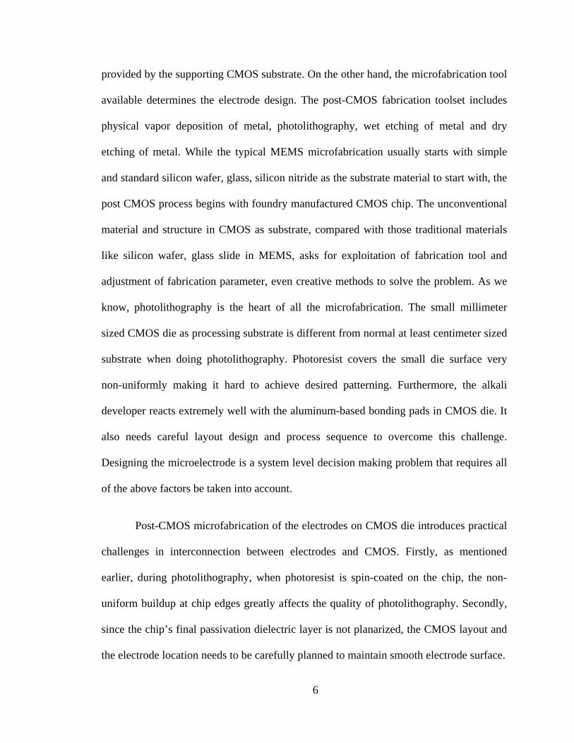
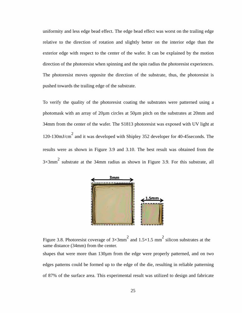
To verify the quality of the photoresist coating the substrates were patterned using a
photomask with an array of 20µm circles at 50µm pitch on the substrates at 20mm and
34mm from the center of the wafer. The S1813 photoresist was exposed with UV light at
120-130mJ/cm2 and it was developed with Shipley 352 developer for 40-45seconds. The
results were as shown in Figure 3.9 and 3.10. The best result was obtained from the
3×3mm2 substrate at the 34mm radius as shown in Figure 3.9. For this substrate, all
shapes that were more than 130µm from the edge were properly patterned, and on two
edges patterns could be formed up to the edge of the die, resulting in reliable patterning
of 87% of the surface area. This experimental result was utilized to design and fabricate
Figure 3.8. Photoresist coverage of 3×3mm2 and 1.5×1.5 mm
2 silicon substrates at the
same distance (34mm) from the center.

26
post-CMOS electrode arrays for biosensor applications. This provided the guideline of
how much estate is available on the substrate surface and where the electrodes could be
placed and clearly patterned.
Figure 3.10. 20µm diameter circle array with 50µm period photoreisist patterned on
3×3mm2 substrates at 34mm from the center of the wafer.
Figure 3.9. 20µm diameter circle array with 50µm period photoreisist patterned on
3×3mm2 substrates at 20mm from the center of the wafer.
27
Design and development of on chip electrode array for electrochemical biosensor
3.2.3 Gold as the electrode material
To form an on-chip microelectrode array, gold is an outstanding metal because it can
readily be deposited and patterned, is inert and biocompatible in a biosensing liquid
environment, and permits immobilization of biointerfaces using well established adhesion
chemistry. The on-chip electrode could be fabricated using an electroless nickel
immersion gold process that replaces the aluminum layer from a standard CMOS process
[50]. However, the deposition thickness of gold is difficult to control with this method
due to its deposition mechanism, and the process is prone to poor reproducibility because
of variable aluminum alloy composition across a chip and between different chips. Also
the gold follows the topology of the original aluminum alloy so that the gold is relatively
rough. Our experimental efforts with this deposition process have resulted in a non-
uniform gold layer with high surface roughness. Alternatively, the on-chip microelectrode
array could be fabricated using conventional physical vapor deposition (PVD) and
photolithography, which provides precise control of electrode thickness and area. With
this method, the roughness of the gold is subject to the surface profile of the CMOS chip,
which is typically passivated by a flat silicon dioxide layer. For many protein-based
biosensors, the electrode roughness is a critical parameter. For example, a biosensor
utilizing a bio-mimetic tethered lipid bilayer membrane must have a very smooth surface
to prevent pinholes in the self assembled lipid bilayer.

28
3.2.4 Design consideration of electrode geometry
To enable electrochemical measurement, each element of the on-chip array includes
a WE, CE and RE. Development of a reliable planar reference electrode remains a
research challenge, and a pseudo RE was chosen so that all electrodes could be formed
using Au. Figure 3.11 describes the electrode pattern that was designed to maximize the
electrochemical response current and realize uniform ion flow by arranging the electrodes
concentrically. The distance between WE and CE is kept small to minimize errors due to
potential drop in the solution and to speed up charging of the double layer capacitance
thus providing faster steady-state sensor response [55]. Reducing the distance between
RE and WE minimizes the IR (current-resistant product) loss to allow better control of
WE potential. The RE could be placed where CE-WE current is low to minimize the
current contribution of IR loss [55]. The working electrode is relatively large to maximize
sensor area, and the size can easily be modified to suit different biosensor interfaces
based on the electrochemical current level (which is a function of WE area) and desired
Figure 3.11. Single element of an electrode array consisting of WE, RE and CE.

29
array density.
3.2.5 Development of post-CMOS die-level electrode fabrication
The die-level post-CMOS fabrication process begins with formation of the electrode
array on the CMOS chip. It is referred to as die-level processing because it is received
from the foundry and individual die is processed. But the same processes can be applied
at a wafer scale.
The process was done in Keck microfabrication facility in Michigan State University.
The metal was deposited on the die by thermal evaporation of titanium/gold (50Å/1000Å)
using physical vapor deposition equipment where titanium played as adhesion layer. The
current required for titanium evaporation was 2.2A and the deposition rate was
approximately 0.1Å/s. For gold the current was 2.4A and deposition rate was about
0.7Å/s. Obviously, the deposition rate depended on the heating temperature thus the
flowing current in evaporation boat. The base pressure in the evaporation chamber was
5×10⁻⁷
torr. Lower base pressure can offer lower evaporation temperature and less
Figure 3.12. Process flow for post-CMOS electrode fabrication: Ti/Au is deposited and patterned (a-b), Polyimide is spin coated and patterned (c-d).

30
contamination due to enhanced mean free path of molecules and lower vapor pressure.
The gold and titanium was then patterned by wet etching using standard
photolithography. The procedure described in section 3.2 was employed for the
photolithography and photomask design. The die was bonded to the perimeter of a 3-inch
silicon wafer to do the photoresist spin coating. Potassium iodide solution and buffered
hydrofluoric acid was chosen as the etchants for gold and titanium, respectively. The gold
was left on bonding pads and electrode contacts because the original metal aluminum
alloy was very reactive with following alkali photoresist developer and even with water.
Apparently if the aluminum alloy had corroded during photoresist developing the circuit
chip could have been damaged detrimentally and the byproduct of the reaction could
have contaminated the surface electrodes. Polyimide was then spin coated on the CMOS
chip surface and patterned to insulate electrode routing and define the electrode area.
Polyimide exhibited good coverage on planar surface. Polyimide was an excellent
insulation material used in electronics, for example, a lot of ribbon cables were insulated
by polyimide. Polyimide was patterned in a way that electrodes and bonding pads were
exposed so that electrodes could be reached by solution and bonding pads could be wire
bonding. The polyimide was then baked in 2 steps, 30mins at 200°C followed by 30mins
at 300°C. Both steps were ramping up and down gradually from and to room temperature
to avoid cracks in the polyimide caused by unmatched thermal expansion coefficient
between polyimide and silicon. The die-level process steps are illustrated in Figure 3.12.
At the end of this process, the electrode array has been formed and the chip surface
has been passivated everywhere except the desired electrode areas and the wire bond

31
pads. Thus the wire bond pads can be used for wire bonding later. The CMOS die was
then ready to go through the subsequent packaging process that was specifically designed
for operation in liquid environment. The background and procedures of the packaging
will be described in detail in chapter 4.
3.2.6 Preliminary results of post-CMOS die-level electrode fabrication
A few designs were realized using the approach described in section 3.2 including
electrode arrays up to 10×10 and interdigitated electrodes, etc. A single 1mm electrode,
2×4 electrode array, 10×10 100µm (diameter) electrode array and 20µm gap
interdigitated electrode were successfully fabricated on 3×3mm2 CMOS die. These
Figure. 3.13. Different electrode designs fabricated on CMOS chip including 10×10 100µm diameter electrode array, 20µm gap interdigitated electrode and electrodes for electrochemical measurements.

32
results verified the viability of the die-level processing technique and show the potential
applications in on-chip electrochemical sensing with different sensing needs. The
fabricated electrodes are as shown in Figure 3.13.

33
4 Development of post-CMOS packaging fabrication
4.1 Requirements of post-CMOS packaging for electrochemical biosensor
The integrated die of electrode array and CMOS electronics should be able to
operate in an aqueous biological environment and measure the bio-activity on the
electrode surface in real time using the CMOS electronics. Thus, there are requirements
for biointerface assembly and operation in a liquid environment that constrain the
materials and structures available for packaging.
Operation of the CMOS biosensor array in an aqueous environment establishes a
critical requirement to insulate all surfaces of the CMOS device in contact with the liquid.
The small surface area available on a CMOS chip necessitates either a complex fluid
handling system or packaging of the entire chip for immersion in liquid. Because the
chip’s surface must remain accessible for biointerface formation and sensor operation,
flip-chip packaging and other approaches that similarly bury I/O bondpads cannot be
employed in a straightforward manner. Also, those general surface or bulk
micromachining technique in MEMS could be not directly applied to the packaging
process without custom modification because of the complicated structures of packaging.
Alternatively, a chip-in-package approach utilizing wire-bonded die was adopted in
this work, establishing a need for a protective insulating material capable of coating all
surfaces of the 3D chip structure, including chip sidewalls and wirebonds. At the same
time, the packaging approach must permit patterning of the 2D chip-electrode surface and
cleaning of electrodes to remove any metal ions or contaminants before biointerface

34
assembly. For example, our experiments have shown that aggressive electrode cleaning
by piranha solution and organic cleaning are required for reliable self assembly of
nanostructured biointerfaces. The packaging material must therefore withstand the strong
corrosiveness of piranha solution. Several materials were studied to meet these demands.
Mainly, three packaging materials were investigated, tested and compared including SU-8,
polyimide and parylene.
4.2 Packaging materials
4.2.1 SU-8
SU-8 photoresist is widely used in MEMS fabrication; it is available in a wide range
of viscosities and is suitable to form thick layers and high aspect ratio structures [56].
Figure 4.1. Chip packaging flow: (a) chip in DIP40 package; (b) dispense SU8 2002 using a syringe; (c) soft baking, UV exposure and hard baking; (d) final SU8 reservoir; (e) PDMS cap and DIP40 package. Steps (b) and (c) are repeated 4 or 5 times until package is fully filled with SU8.
PDMS
UV exposure

35
Previously, SU-8 was used as the packaging material for use in liquids in our work [57].
In [57], the DIP40 ceramic package was used to package the CMOS die. In order to
perform on-CMOS test in water, the area around the chip, inside the DIP40 package, was
filled with SU8 photoresist. The SU8 was applied through a syringe in several layers, soft
baking on a hotplate and cross linking with UV light after each layer, as shown in Figure
4.1. The final SU8 layer isolated the wire bonds and created a reservoir of approximately
0.5ml was formed above the chip, as shown in Figure 4.2(a). However, when tested
experimentally, cracks were observed after prolonged soaking in an aqueous environment.
Figure 4.2(b) shows cracks that developed near the pad area and caused corrosion of the
bonding pads that rendered the chip useless.
4.2.2 Polyimide
Polyimide is another insulating polymer material widely used in bioMEMS
packaging applications, although it cannot achieve layers as thick as SU-8. Polyimide can
be applied by spin coating and curing in a low temperature oven. It is easy to pattern
using either wet or dry etching, and our tests indicate it provides excellent coverage and
uniformity on 2D flat surfaces and survives prolonged use in an aqueous environment.
However, when tested for coverage of 3D structures like a wirebonded chip, cracks in the
polyimide layer due to shrinkage during curing were observed. Figure 4.3(c) shows a
polyimide-coated CMOS chip with large cracks (light color within the dotted line) where
the polyimide layer approaches wirebonds on the chip’s periphery (dark color within
dotted line).

36
4.2.3 Parylene
Parylene, or poly (p-xylylene), is a thin film polymer that is also popular for
insulating electronics. Parylene is chemically inert, permits conformal coating and has
excellent barrier properties. Parylene C (poly(monochloro-p-xylylene)) has the highest
possible biocompatibility rating among polymers for long term implants and has an
extensive history of use in the medical industry. Because of its biocompatibility,
biostability, low cytotoxicity and resistance against hydrolytic degradation, Parylene C
has been widely used in micro/nano-fabricated devices and microfluidics. Parylene C
utilizes a simple chemical vapor deposition method with low process temperature and is
compatible with standard microfabrication processes. Our experiments have shown that
parylene successfully overcomes the problems associated with SU-8 and polyimide, no
cracking and uniform coverage, providing an excellent coating of 3D structures like wire-
bonded chips.
4.3 Post-CMOS packaging process
As introduced in section 4.2.3, parylene has the properties suitable for biological
(a) (b) (c)
Figure 4.2. (a) A CMOS chip packaged using SU8 with electrodes exposed; (b) A crack in SU8 observed at the interface of the chip and SU8 where leakage occurs; (c) A polyimide coating on the surface of a packaged chip that cracked after hard baking.

37
applications. Besides, parylene can be deposited isotropically at low temperature. The
parylene is usually patterned by dry etching using photoresist or other dielectric as
masking layer made by photolithography. In our research, the CMOS chip was wire
bonded to package body and the whole CMOS chip and bonding wires needed to be
coated with parylene while the on-CMOS electrodes should be exposed for access to
form bio-interface on the electrodes. To expose the electrodes, or to selectively etch away
the parylene above the electrodes, normal masking method by photolithography was not
feasible any longer because the 3D structured package could not be spin-coated by
photoresist uniformly and consistently. Thus, a rapid proto-typing parylene etching steps
were developed to achieve the parylene packaging.
The CMOS die with on-CMOS electrode array fabricated in chapter 3 was mounted
and wire bonded to a standard PGA108 (pin grid array 108) ceramic package. Figure 4.3
describes the package-level post-CMOS process. After the CMOS chip was wire bonded,
the whole package with CMOS chip was then coated with a 5µm layer of parylene using
PVD (PDS 2035CR, Specialty Coating Systems). This process covered all surfaces
within the package, including bonding wires, package contact pads and the electrode
array chip. Next, parylene needed to be removed from the electrode array area while
leaving all other surfaces coated. Parylene was generally etched by reactive ion etching
(RIE) using oxygen gas with photoresist or another solid layer deposited and patterned to
form a masking layer. However, in this complex three-dimensional structure, such
methods cannot meet masking requirement, and a customized etching process was
developed to overcome this challenge. First, a hole punch was used to create a cylinder of
cured PDMS (polydimethylsiloxane) sized to match the area of the chip’s surface from
38
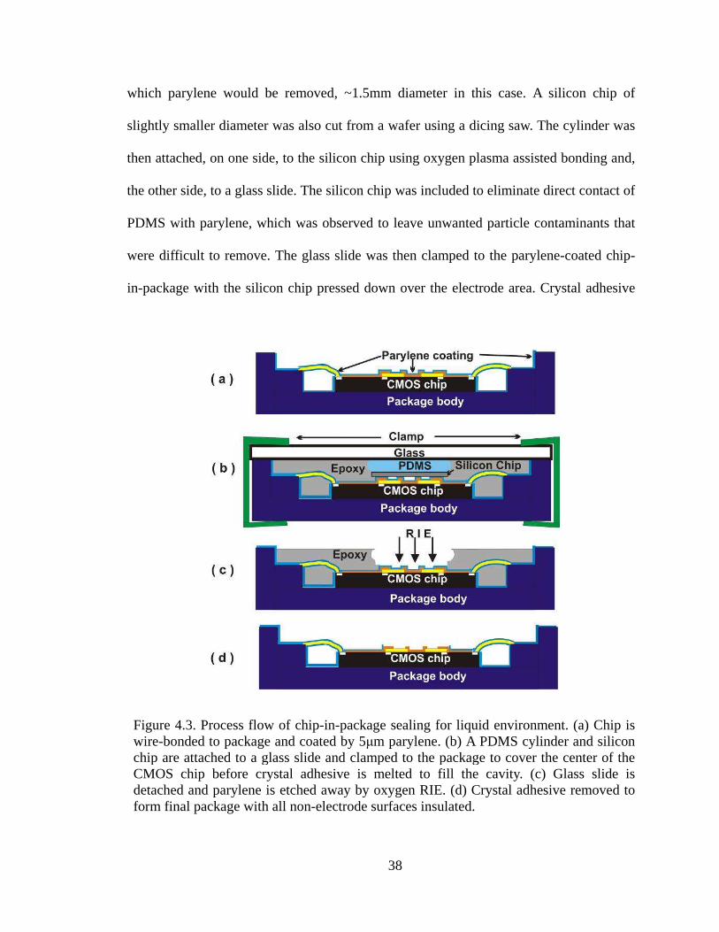
which parylene would be removed, ~1.5mm diameter in this case. A silicon chip of
slightly smaller diameter was also cut from a wafer using a dicing saw. The cylinder was
then attached, on one side, to the silicon chip using oxygen plasma assisted bonding and,
the other side, to a glass slide. The silicon chip was included to eliminate direct contact of
PDMS with parylene, which was observed to leave unwanted particle contaminants that
were difficult to remove. The glass slide was then clamped to the parylene-coated chip-
in-package with the silicon chip pressed down over the electrode area. Crystal adhesive
Figure 4.3. Process flow of chip-in-package sealing for liquid environment. (a) Chip is wire-bonded to package and coated by 5µm parylene. (b) A PDMS cylinder and silicon chip are attached to a glass slide and clamped to the package to cover the center of the CMOS chip before crystal adhesive is melted to fill the cavity. (c) Glass slide is detached and parylene is etched away by oxygen RIE. (d) Crystal adhesive removed to form final package with all non-electrode surfaces insulated.

39
(Crystalbond 509, SPI supplies) was then inserted into the cavity beneath the slides and
melted at 120˚C to fill the cavity except where the PDMS/silicon cylinder was held
(Figure 4.3(b)). Later, the slide/PDMS/silicon assembly was removed leaving parylene
everywhere except the interior of chip’s surface where previously deposited polyimide
remains to insulate surface routing and leave only the electrodes exposed. Parylene was
then etched using RIE, with 300W RF power and 500sccm oxygen flow rate, to expose
the desired electrode surfaces (Figure 4.3(c)). Once the crystal adhesive was removed
using acetone, the final package provided exposed electrode with all other surfaces
coated with parylene (Figure 4.3(d)).
4.4 Discussion
This packaging method used parylene as the insulation material so that it had the
advantageous properties of parylene itself while it could accomplish the goal of insulation
and protection. The parylene did not crack like SU-8 and uniformly covered the every
surface. Those works using epoxy to insulate chips [46-50] relied on hand manipulation
to apply epoxy to define exposed are which was prone to error and not reproducible
because the epoxy used cured permanently and was almost not removable. However, in
this packaging method exposed area could be accurately controlled by the size of the
silicon chip and every fabrication step was reversible so that it allowed correction of
errors occurring during fabrication and enhanced the fabrication yield. To our best
knowledge, the only reported CMOS packaging using parylene used laser source to
scribe the parylene [51]. The laser source was not one of the standard cleanroom tools
and the dose of the laser should be carefully selected to cut parylene but not damage
CMOS chip. In comparison, RIE is a typical cleanrooom dry etching tool and the etching

40
rate of parylene could be easily characterized. However, our method required heating of a
crystal adhesive that dissolved by acetone, PDMS and manual manipulation of clamping.

manufactured by MOSIS and the chip is as shown in Fi
was fabricated on chip
included a WE, CE and RE that were connected to the CMOS circuit by routing gold
traces to surface contact openings. All surface CMOS cont
to protect them during photoresist development. The polyimide insulation layer was then
coated, patterned and cured to insulate the surface while exposing electrodes and bonding
pads. The chip was then bonded to a
bonded. Next, parylene was deposited on the packaged chip and etched so that all
5.1
A multi
manufactured by MOSIS and the chip is as shown in Fi
was fabricated on chip
included a WE, CE and RE that were connected to the CMOS circuit by routing gold
traces to surface contact openings. All surface CMOS cont
to protect them during photoresist development. The polyimide insulation layer was then
coated, patterned and cured to insulate the surface while exposing electrodes and bonding
pads. The chip was then bonded to a
bonded. Next, parylene was deposited on the packaged chip and etched so that all
Figure 5.1waveform generator and 4
5
5.1 Post
A multi-function amperometric instrumentation chip (MAIC)
manufactured by MOSIS and the chip is as shown in Fi
was fabricated on chip using
included a WE, CE and RE that were connected to the CMOS circuit by routing gold
traces to surface contact openings. All surface CMOS cont
to protect them during photoresist development. The polyimide insulation layer was then
coated, patterned and cured to insulate the surface while exposing electrodes and bonding
pads. The chip was then bonded to a
bonded. Next, parylene was deposited on the packaged chip and etched so that all
Figure 5.1. The waveform generator and 4
On-CMOS
ost-CMOS electrode fabrication and packaging
function amperometric instrumentation chip (MAIC)
manufactured by MOSIS and the chip is as shown in Fi
using methods described in
included a WE, CE and RE that were connected to the CMOS circuit by routing gold
traces to surface contact openings. All surface CMOS cont
to protect them during photoresist development. The polyimide insulation layer was then
coated, patterned and cured to insulate the surface while exposing electrodes and bonding
pads. The chip was then bonded to a
bonded. Next, parylene was deposited on the packaged chip and etched so that all
. The 3×3mm2 CMOS amperometric instrumentation chip with
waveform generator and 4-channel potentiostat and amperometric readout array.
41
CMOS electrochemical
CMOS electrode fabrication and packaging
function amperometric instrumentation chip (MAIC)
manufactured by MOSIS and the chip is as shown in Fi
methods described in
included a WE, CE and RE that were connected to the CMOS circuit by routing gold
traces to surface contact openings. All surface CMOS cont
to protect them during photoresist development. The polyimide insulation layer was then
coated, patterned and cured to insulate the surface while exposing electrodes and bonding
pads. The chip was then bonded to a PGA108 package with conductive epoxy and wire
bonded. Next, parylene was deposited on the packaged chip and etched so that all
CMOS amperometric instrumentation chip with channel potentiostat and amperometric readout array.
electrochemical
CMOS electrode fabrication and packaging
function amperometric instrumentation chip (MAIC)
manufactured by MOSIS and the chip is as shown in Figure 5.1.
methods described in chapter 3
included a WE, CE and RE that were connected to the CMOS circuit by routing gold
traces to surface contact openings. All surface CMOS contact pads were covered in gold
to protect them during photoresist development. The polyimide insulation layer was then
coated, patterned and cured to insulate the surface while exposing electrodes and bonding
package with conductive epoxy and wire
bonded. Next, parylene was deposited on the packaged chip and etched so that all
CMOS amperometric instrumentation chip with channel potentiostat and amperometric readout array.
electrochemical array
CMOS electrode fabrication and packaging
function amperometric instrumentation chip (MAIC) was designed and
gure 5.1. A 2×2 electrode array
chapter 3. The four electrodes each
included a WE, CE and RE that were connected to the CMOS circuit by routing gold
act pads were covered in gold
to protect them during photoresist development. The polyimide insulation layer was then
coated, patterned and cured to insulate the surface while exposing electrodes and bonding
package with conductive epoxy and wire
bonded. Next, parylene was deposited on the packaged chip and etched so that all
CMOS amperometric instrumentation chip with channel potentiostat and amperometric readout array.
CMOS electrode fabrication and packaging
was designed and
A 2×2 electrode array
. The four electrodes each
included a WE, CE and RE that were connected to the CMOS circuit by routing gold
act pads were covered in gold
to protect them during photoresist development. The polyimide insulation layer was then
coated, patterned and cured to insulate the surface while exposing electrodes and bonding
package with conductive epoxy and wire
bonded. Next, parylene was deposited on the packaged chip and etched so that all
CMOS amperometric instrumentation chip with

42
surfaces were covered by parylene except the sensor electrode array area. The final
packaged CMOS chip with electrode array is shown in Fig. 5.2. This package scheme is
suitable for subsequent integration with microfluidic channels mounted either to the chip
or to the package. The wire bond contact pads are the most vulnerable area in this type of
packaging.
To evaluate the package sealing, the chip was powered up and successfully tested
after a water drop was dispensed on the chip. Subsequently, the packaged chip was
exposed to piranha solution to clean the electrode array, verifying the capability to
withstand the aggressive chemical processing necessary before protein biosensor
interface formation on the electrodes.
Figure 5.2. Photograph of a CMOS biosensor array chip-in-package and close up views of the post-CMOS surface electrode array.

43
5.2 Bio-interfaces on CMOS-compatible electrodes
5.2.1 PpcA bio-interface on gold electrode array
Microelectrode array was fabricated on silicon substrate using the same CMOS-
compatible process to investigate bio-interfaces. A 10-element gold electrode array of
1mm and 500µm (diameter) was fabricated on silicon substrate as shown in Figure 5.3.
The actual electrode area could be adjusted by deposition and patterning of the insulating
silicon nitride layer. a cytochrome protein biointerface was formed on the gold electrode.
PpcA, a periplasmic Cytochrome C, was expressed heterogeneously in e. coli and
purified using cation exchange chromatography. The biointerface was prepared by
cleaning WE gold electrode surface and contacting it with ethanolic solution of 5mM 11-
mercaptoundecanoic acid and 11-mercaptoundecanol (1:3 ratio) to form a self-assembled
monolayer. PpcA was then immobilized on the self-assembled monolayer by covalent
bonding with 50mM EDC (N-(3-dimethylaminopropyl)-N'-ethylcarbodiimide) and 5mM
NHS (N-hydroxysuccinimide) solution. Unbound PpcA was washed with 20mM
Figure 5.3. 10-element gold electrode array is fabricated on silicon substrate. Two are 1mm of diameter and the rest are 500µm of diameter.

44
phosphate buffer. A commercial platinum CE and a Ag/AgCl liquid junction RE were
used to take cyclic voltammetry. A clear oxidation and reduction peaks were observed
after successful immobilization of PpcA on the gold electrodes as shown in Figure 5.4.
5.2.2 Fabrication of tethered bilayer lipid membrane (tBLM) on
microelectrode and tBLM interaction with nanoparticle (NPs)
To better understand the role and behavior of cell membrane, tethered bilayer lipid
membrane (tBLM) becomes a very useful bio-mimetic interface. By using our fabricated
CMOS-compatible planar gold electrode, tBLM was constructed and its interaction with
nanoparticle (NPs) was studied.
A self-assembled monolayer (SAM) of 1,2-dipalmitoyl-sn-glycero-3-
phosphothioethanol (DPPTE) was formed on a 1mm diameter gold electrode patterned on
Figure 5.4. Cyclic voltammetry of buffer solution (red) and after PpcA immobilized (blue).
45
silicon wafer after cleaning gold electrode in piranha solution (51% H2SO4: 30% H2O2 =
7:3) for 30s. Small unilamellar vesicle (SUV) liposome of 1,2-dioleoyl-sn-glycero-3-
phosphocholine (DOPC) adsorbed and ruptured on SAM to deposit upper leaflet of tBLM.
After tBLM formation, 200 µg/ml F type multi wall carbon nanotubes (F-MWNT of 82
nm in diameter) were added into electrolyte solution and mixed to interact with tBLM
after sonication for 15mins. Electrochemical impedance spectroscopy was used to
characterize tBLM formed on microelectrode and tBLM interaction with F-MWNT over
the frequency range from 0.01 Hz to 100 Hz at 0V bias potential in a two-electrode setup.
Figure 5.4 shows that bode plots of impedance spectra measured by potentiostat (CH
Instruments, Inc). The impedance magnitude of tBLM reached up to 10 MΩ, suggesting a
highly insulating tBLM formed on the gold electrode. To investigate the interaction of
tBLM with carboxylic acid group modified F-MWNT, impedance was recorded
immediately after addition of F-MWNT. An impedance drop was observed as shown in
Figure 5.5, implying transient pores induced by F-MWNT allowing ions to pass through
lipid bilayer. So the impedance decrease after addition of F-MWNT confirmed that F-
MWNT could enhance the ion transport across lipid bilayer.

46
5.3 On-chip electrochemical measurements
To verify the functionality of parylene packaging, a test setup composed of an
MAIC chip, a packaged on-chip electrode array, and a PC with a DAQ card and a
LabVIEW user interface was prepared. A typical electrolyte solution with 1M potassium
chloride and 0.5mM potassium ferricyanide was prepared, and cyclic voltammetry
measurements were performed at 25°C using an on-chip WE, a commercial liquid
junction Ag/AgCl RE and a platinum CE. Figure 5.6 shows the results from both a
commercial potentiostat (CHI760C, CH Instruments Inc.) and the MAIC at scan rates of
100mV/s and 200mV/s. In cyclic voltammetry, the peak locations give important
information for biochemical identification, and these results demonstrate that the peak
locations and amplitudes of the CMOS system compare extremely well with the
commercial system even at different scan rates. In another experiment, a second solution
Figure 5.5. Electrochemical impedance measurements of tBLM and tBLM after FMWNT interaction on a planar gold electrode.
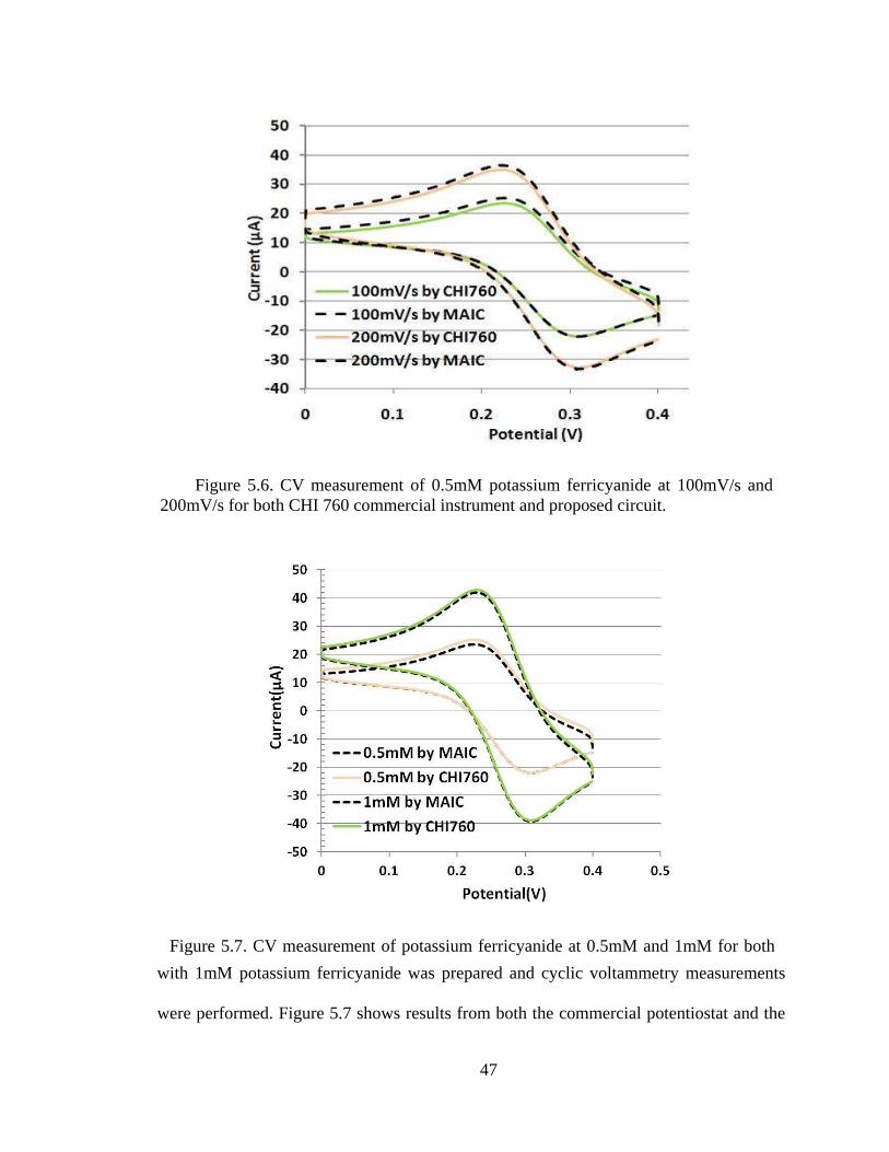
47
with 1mM potassium ferricyanide was prepared and cyclic voltammetry measurements
were performed. Figure 5.7 shows results from both the commercial potentiostat and the
Figure 5.6. CV measurement of 0.5mM potassium ferricyanide at 100mV/s and 200mV/s for both CHI 760 commercial instrument and proposed circuit.
Figure 5.7. CV measurement of potassium ferricyanide at 0.5mM and 1mM for both CHI 760 commercial instrument and proposed circuit.

48
reported CMOS amperometric system at two different electrolyte concentrations. As
expected, the peak current increased with electrolyte concentration, and again the peak
locations and amplitudes of the CMOS system compare extremely well with the
commercial system. These experiments verify the proper operation of the MAIC, the
functionality of the post-CMOS electrodes, and the suitability of the parylene-based
packaging for operation in liquid environments.

49
6 Summary
Miniaturized biosensor arrays are promising by enabling parallel analysis of
multiple parameters. Instead of bulky benchtop instrumentation, integration of CMOS
technology and biosensor allows the sensing and measurements monolithically.
Multidisciplinary knowledge is needed to integrate biosensor, CMOS IC, and packaging
into one single chip. A post-CMOS die-level electrode fabrication and packaging scheme
were developed and the CMOS amperometric instrumentation system with on-chip
electrode array and packaging were realized. Post-CMOS fabrication process was
described for forming an on-chip electrode array suitable for protein-based biosensors
and parylene packaging suitable for operation in a liquid environment. Functionality of
the overall system was verified by performing cyclic voltammetry in a potassium
ferricyanide solution. The on-chip instrumentation circuits successfully performed
electrochemical measurements at different scan rates and electrolyte concentrations. The
instrumentation circuitry and post-CMOS fabrication processes reported here are suitable
for forming single-chip electrochemical analysis microsystems with a wide range of
biological and chemical sensor interfaces achieving the thesis goal.
The main contributions of this thesis research are:
Contribution 1: First experiments and characterization of CMOS-compatible die-
level photolithography for on-CMOS planar electrode fabrication
The traditional wafer-scale fabrication methods are not suitable die-level substrate
because of the edge bead effect during spin coating. In this thesis, for the first time die-

50
level photolithography was experimentally characterized and the post-CMOS die-level
fabrication process of on-chip electrode array was developed. A few electrode designs
were successfully fabricated using the developed methods.
Contribution 2: Developed first rapid prototyping of on-CMOS biosensor array
packaging for electrochemical measurement in liquid environments using parylene
The integration of on-chip biosensor and electrochemical CMOS circuits is
attractive but challenging because of the liquid experiment environment. A parylene-
based packaging method was developed and verified and allowed on-CMOS
electrochemical measurement in liquid environments.
Contribution 3: First monolithic integration of CMOS and electrochemical
biosensor for in-situ on-CMOS measurement tailored for tBLM interface
Even though some integrated CMOS biosensor systems were reported, it is the first
time the integration was specifically designed and implemented towards on-CMOS
formation of tether bilayer lipid membrane biointerface (tBLM). The unique tBLM
biointerface imposes higher requirements on the electrode quality including ultra-smooth
and clean gold electrode surface, accurately defined electrode area, and strict electrode
cleaning. The method in this thesis was designed to accommodate these requirements and
achieved the monolithic system integration.

51
APPENDIX

52
Gold electrode fabrication procedure
1. Metal deposition
Use physical vapor deposition equipment in KECK facility
i. Load Titanium and gold into the designated boats
ii. Load the sample substrate
iii. Close the chamber and pump down until less than 10-6
Torr
iv. Select the Titanium boat and turn on the current switch
v. Slowly increase current, 1Ampere per 5minutes, set at 3.6Ampere and
0.1Å/s deposition rate
vi. Open the shutter and start deposition
vii. Once the deposition is done, close the shutter and slowly lower the
current
viii. Similarly, do the gold deposition, at 2.2Ampere and 1.0 Å/s
2. Electrode pattern
i. Spin coat the Shipley 1813 positive photoresist at 3000rpm for
60seconds
ii. Soft bake the photoresist for 1min at 110°C on hotplate
iii. UV exposure for 130-150mJ/cm2 through designed photomask
iv. Develop the photoresist using Developer 352
v. Hard bake the photoresist for 1min at 110°C on hotplate
vi. Etch the gold using potassium iodide+ iodine etchant

53
vii. Etch the titanium using buffered hydrofluoric acid, wear the protection
facemask, thick rubber glove and apron
viii. Rinse away the photoresist using acetone and DI water
ix. Blow dry with compressed nitrogen gun

54
BIBLIOGRAPHY

55
Bibliography
[1] K. Rogers, "Biosensors for environmental monitoring a regulatory perspective," TrAC Trends in Analytical Chemistry, vol. 14, no. 14, pp. 289-294, 1995.
[2] M. Keusgen, "Biosensors: new approaches in drug discovery," Naturwissenschaften, vol. 89, no. 89, pp. 433-444, 2002.
[3] J. Wang, "Amperometric biosensors for clinical and therapeutic drug monitoring: a review," Journal of Pharmaceutical and Biomedical Analysis, vol. 19, no. 19, pp. 47-53, 1999.
[4] I. Moser, G. Jobst, and G. A. Urban, "Biosensor arrays for simultaneous measurement of glucose, lactate, glutamate and glutamine," Biosensors and Bioelectronics, vol. 17, no. 17, pp. 297-302, 2002.
[5] W. R. Leifert, A. L. Aloia, O. Bucco, R. V. Glatz, and E. J. McMurchie, "G-Protein-Coupled Receptors in Drug Discovery: Nanosizing Using Cell-Free Technologies and Molecular Biology Approaches," Journal of Biomolecular Screening, vol. 10, no. 10, pp. 765-779, December 1, 2005 2005.
[6] F. M. Marassi and S. J. Opella, "A solid-state NMR index of helical membrane protein structure and topology," Journal of Magnetic Resononce, vol. 144, no. 144, pp. 150-155, 2000.
[7] W. R. Leifert, A. L. Aloia, O. Bucco, R. V. Glatz, and E. J. McMurchie, "G-protein-coupled receptors in drug discovery: nanosizing using cll-free technologies and molecular biology approaches," J. Biomol Screen, vol. 10, no. 10, pp. 765-779, 2005.
[8] P. Arenkov, A. Kukhtin, A. Gemmell, S. Voloshchuk, V. Chupeeva, and A. Mirzabekov, "Protein Microchips: Use for Immunoassay and Enzymatic Reactions," Analytical Biochemistry, vol. 278, no. 278, pp. 123-131, 2000.
[9] G. MacBeath and S. L. Schreiber, "Printing proteins as microarrays for high-throughput function determination," Science, vol. 289, no. 289, pp. 1760-1763, 2000.
[10] C. Bertucci and S. Cimitan, "Rapid screening of small ligand affinity to human serum albumin by an optical biosensor," Journal of Pharmaceutical and Biomedical Analysis, vol. 32, no. 32, pp. 707-714, 2003.
[11] P. Arenkov, A. Kukhtin, A. Gemmell, S. Voloshchuk, V. Chupeeva, and A. Mirzabekov, "Protien microchips: use for immunoassay and enzymatic reactions," Analytical Biochemistry, vol. 278, no. 278, pp. 123-131, 2000.
[12] D. Guschin, G. Yershov, A. Zaslavsky, A. Gemmell, V. Shick, D. Proudnikov, P.

56
Arenkov, and A. Mirzabekov, "Manual manufacturing of oligonucleotide, DNA, and protein microchips," Analytical Biochemistry, vol. 250, no. 250, pp. 203-211, 1997.
[13] K. E. Gonsalves, C. L. Laurencin, C. R. Halberstadt, and L. S. Nair, Biomedical nanostructures: New York: John Wiley & Sons Inc, 2008, pp. 442.
[14] A. J. Bard and L. R. Faulkner, Electrochemical methods: Wiley, 1980.
[15] B. Jang and A. Hassibi, "Biosensor systems in standrard CMOS processes fact or fiction?," IEEE Symp. Industrial Electronics, 2008, pp. 2045-2050.
[16] A. P. F. Turner, I. Karube, and G. S. Wilson, Biosensors, Fundamentals and Applications: Oxford University Press, 1987.
[17] P. Mulchandani, A. Mulchandani, I. Kaneva, and W. Chen, "Biosensor for direct determination of organophosphate nerve agents: 1. Potentiometric enzyme electrode," Biosens. Bioelectron., no. pp. 77-85, 1999.
[18] R. Yuan, D. Tang, Y. Chai, X. Zhong, Y. Liu, and J. Dai, "Ultrasensitive potentiometric immunosensor based on SA and OCA techniques for immobilization of HBsAb with colloidal Au and polyvinyl butyral as matrixes," Langmuir, no. pp. 7240-7245, 2004.
[19] B. A. Gregg and A. Heller, "Glucose-oxidase for amperometric biosensor applications," Anal. Chem., no. pp. 258-263, 1990.
[20] S. A. Emr and A. M. Yacynych, "Use of polymer films in amperometric biosensors," vol. 7, no. 7, 1995.
[21] J. J. Gooding, L. Pugliano, D. B. Hibbert, and P. Erokhin, "Amperometric biosensor with enzyme amplification fabricated using self-assembled monolayers of alkanethiols: the influence of the spatial distribution of enzymes," Electrochem. Commun., no. pp. 217-221, 2000.
[22] M. S. Alaejos and F. J. G. Montelongo, "Application of amperometric biosensors to the determination of vitamins and a-amino acids," Chem. Rev., no. pp. 3239-3266, 2004.
[23] B. Priento-Simon and E. Fabregas, "Comparative study of electron mediators used in the electrochemical oxidation of NADH," Biosens. Bioelectron., no. pp. 1131-1138, 2004.
[24] A. Heller, "Electrical connection of enzyme redox centers to electrodes," J. Phys. Chem., no. pp. 3579-3587, 1992.
[25] S. Frretti, S. Paynter, D. A. Russell, K. E. Sapsford, and D. J. Richardson, "Self-

57
assembled monolayers: a versatile tool for the formulation of bio-surfaces," Trends Anal. Chem., no. pp. 530-540, 2000.
[26] J. J. Gooding, et al., "Parameters important in fabricating enzyme electrodes using self-assembled monolayers of alkanethiols," Anal. Sci., no. pp. 3-9, 2001.
[27] S. Sampath and O. Lov, "Inert metal-modified, composite ceramic-carbon amperometric biosensors: renewable, controlled reactive layer," Anal. Chem., no. pp. 2015-2021, 1996.
[28] R. Garjonyte and A. Malinauskas, "Amperometric glucose biosensor based on glucose oxidase immobilized in poly(o-phenylenediamine) layer," Sensors and Actuators B: Chem., no. pp. 85-92, 1999.
[29] E. A. Irhayem, H. Elzanowska, A. S. Jhas, B. Skrzynecka, and V. Birss, "Glucose detection based on electrochemically formed Ir oxide films," J. Electroanal. Chem., no. pp. 153-164, 2002.
[30] N. K. Chaki and K. Vijayamohaman, "Self-assembled monolayers as a tunable platform for biosensor applications," Biosens. Bioelectron., no. pp. 1-12, 2002.
[31] Z. Cheng, E. Wang, and X. Yang, "Capacitive detection of glucose using molecularly imprinted polymers," Biosens. Bioelectron., no. pp. 179-185, 2001.
[32] F. Mansfeld and W. J. Lorenz, Electrochemical impedance spectroscopy-applications in corrosion science and technology, in: R. Varma, J. R. Selman (Eds.), Techniques for characterization of elecctrodes and electrochemical processes. New York: Wiley, 1991, pp. 581-647.
[33] A. Lasia, Electrochemical impedance spectroscopy and its applications vol. 32. New York: Kluwer Academic/Plenum Press, 1999, pp. 143-248.
[34] G. Inzelt and G. Lang, "Model dependence and reliability of the electrochemical quantities derived from the measured impedance spectra of polymer modified electrodes," J. Electroanal. Chem., no. pp. 39-49, 1994.
[35] J. Benavente, J. R. Ramos-Barrado, and A. Cabeza, "Electrical behaviour of an inorganic film from ac and dc measurements," J. Colloid Interface Sci., no. pp. 116-121, 1996.
[36] T. M. Nahir and E. F. Bowden, "Impedance spectroscopy of electroinactive thiolate films adsorbed on gold," Electrochim. Acta., no. pp. 2347-2352, 1994.
[37] R. P. Janek, W. R. Fawcett, and A. Ulman, "Impedance spectroscopy of self-assembled monolayers on Au(III): evidence for complex double-layer structure in aqueous NaClO4 at the potential of zero charge," J. Phys. Chem. B, no. pp. 8550-858,

58
1997.
[38] L. V. Protsailo and W. R. Fawcett, "Studies of electron transfer through self-assembled monolayers using impedance spectroscopy," Electrochim. Acta., no. pp. 3497-3505, 2000.
[39] A. Bard and L. Faulkner, Electrochemical Methods: Fundamentals and Applications. New York: John Wiley & Sons, 2001.
[40] R. M. Wightman, "Voltammetry with microscopic electrodes in new domains," Science, vol. 240, no. 240, pp. 415-420, 1988.
[41] R. J. Reay, A. F. Flannery, C. W. Storment, S. P. Kounaves, and G. T. A. Kovacs, "Microfabricated electrochemical analysis system for heavy metal detection," Sensors and Actuators B: Chemical, vol. 34, no. 34, pp. 450-455, 1996.
[42] P. Levine, P. Gong, K. Shepard, and R. Levicky, "Active CMOS array for electrochemical sensing of biomolecules," IEEE Custom Integrated Circuits Conference, CICC, 2007, pp. 825-828.
[43] P. M. Levine, P. Gong, R. Levicky, and K. L. Shepard, "Active CMOS sensor array for electrochemical biomolecular detection," Solid-State Circuits, IEEE Journal of, vol. 43, no. 43, pp. 1859-1871, 2008.
[44] A. Frey, et al., "A digital CMOS DNA cihp," IEEE International Symposium on Circuits and Systems, ISCAS, 2005, pp. 2915-2918.
[45] S. Hwang, C. Lafratta, V. Agarwal, X. Yu, D. Walt, and S. Sonkusale, "CMOS microelectrode array for electrochemical Lab-on-a-Chip applications," Sensors Journal, IEEE, vol. 9, no. 9, pp. 609-615, 2009.
[46] U. Frey, et al., "Switch-Matrix-Based High-Density Microelectrode Array in CMOS Technology," IEEE J. Solid-State Circuits, vol. 45, no. 45, pp. 467-482, 2010.
[47] J. M. B. Christen and A. G. Andreou, "Design, fabrication, and testing of a hybrid CMOS/PDMS microsystem for cell culture and incubation," IEEE Trans. Biomed. Circuits Syst., no. pp. 3-18, 2007.
[48] E. Ghafar-Zadeh, M. Sawan, and D. Therriault, "Novel direct-write CMOS-based laboratory-on-chip: design, assembly and experimental results," Sensors and Actuators A: Phys., vol. 134, no. 134, pp. 27-36, 2007.
[49] F. Heer, S. Hafizovic, W. Franks, A. Blau, C. Ziegler, and A. Hierlemann, "CMOS microelectrode array for bidirectional interaction with neuronal networks," IEEE J. Solid-State Circuits, vol. 41, no. 41, pp. 1620-1629, Jul. 2006.

59
[50] A. Manickam, A. Chevalier, M. McDermott, A. D. Ellington, and A. Hassibi, "A CMOS electrochemical impedance spectroscopy(EIS) biosensor array," IEEE. Trans. Biomed. Circuits Syst., vol. 4, no. 4, pp. 379-390, Dec. 2010.
[51] T. Prodromakis, K. Michelakis, T. Zoumpoulidis, R. Dekker, and C. Toumazou, "Biocompatible encapsulation of CMOS based chemical sensors," IEEE Int. Conf. on Sensors, Oct. 2009, pp. 791-794.
[52] S. M. Martin, F. H. Gebara, B. J. Larivee, and R. B. Brown, "A CMOS-integrated microinstrument for trace detection of heavy metals," IEEE J. Solid State Circuits, vol. 40, no. 40, pp. 2777-2786, Dec. 2005.
[53] G. A. Luurtsema, "Spin coating for rectangular substrates," Master of Science, Electrical Engineering and Computer Sciences, University of California, Berkeley, 1997.
[54] G. Carcano, M. Ceriani, and F. Soglio, "Spin coating with high viscosity photoresist on square substrates," Hybrid Circuits, vol. 32, no. 32, p. 12, 1993.
[55] Y. Huang, Y. Liu, B. L. Hassler, R. M. Worden, and A. J. Mason, "A protein-based electrochemical biosensor array platform for integrated microsystems" in press, no. 2011.
[56] X. Liu, L. Li, and A. J. Mason, "Thermal control microsystem for protein characterization and sensing," IEEE Biomedical Circuits Systems Conf., Beijing China, Nov. 2009, pp. 277-280.
[57] X. Liu, L. Li, and A. J. Mason, "Thermal control microsystem for protein characterization and sensing," Bimedical Circuits and systems Conference IEEE, Beijing, 2009, pp. 277-280.