fabrication and characterization of 60 channel ... · fabrication and characterization of 60...
TRANSCRIPT
147Journal of Integrated Circuits and Systems 2016; v.11 / n.3:147-158
Fabrication and Characterization of 60 Channel Microelectrode Arrays for Recording and Stimulation
from Cardiac Cells in CultureVanessa Pereira Gomes1,2, Angelica Denardi de Barros2, João-Batista Destro-Filho3, Sergio Martinoia4,
Alberto Pasquarelli5, and Jacobus Willibrordus Swart1,2
1School of Electr. & Comput. Eng., State University of Campinas, Campinas, Brazil2 Center of Semiconductor Components and Nanotechnologies, State University of Campinas, Campinas, Brazil
3 School of Electr. Eng., Federal University of Uberlândia, Uberlândia, Brazil4Department of Inform.,Bioeng., Robotics and Systems Eng., University of Genoa, Genoa, Italy
5Institute of Electron Devices and Circuits, Ulm University, Ulm, Germanye-mail: [email protected]
ABSTRACT
Stimulation and recording of nerve cells is a procedure used for several applications, such as clinical therapies, study of basic neuroscience, and neural prostheses. Microtechnology and advances in material science have allowed to produce more sophisticated devices and with more functions. This paper focuses on the fabrication of planar 60 – channel Microelectrode Arrays (MEAs). The electrical characterization of the noise level from the TiN electrodes showed good sensitivity to noise, compatible with commercial systems. These electrodes received an artificial electrocardiogram signal (ECG) from a function generator and registered the same input signal but with lower amplitude. Finally, both cyclic voltammetry curves of the produced MEA and the commercial MEA exhibited similar shape, but the current density of the first one was significantly higher than in MCS – MEA, with an order difference of magnitude.
Index Terms: Microelectrodes; Microfabrication; Cell; Recording; Stimulation.
I. INTRODUCTION
Microelectrode Array (MEA), a tool available for both pharmacological applications [1] and electro-physiological measurements [2], was initially a two – dimensional arrangement designed only to extracellu-lar stimulation and monitoring of the electrical activity of electrogenic cells (as neurons of the central nervous system, peripheral muscle cells, and cardiac tissues of humans and animals), tissue slices, and cultures [3]. However, it has been widely used in neuroscience to record spikes from brain slices [4], dissociated neuro-nal [5], retinas [6], and cardiomyocytes cultures [7].
MEA has several advantages, such as non – inva-sively, multisite recording of cell potentials (up to tens of channels), allowing long – term recordings under properly maintenance conditions (from several hours up to months or even a year), and it is also capable to stimulate by applying potential on the electrodes [8, 9].
As the use of MEAs requires being in contact with a quite corrosive medium (human body), the choice of materials is an important step. In general, MEAs must exhibit [10]: biocompatibility (i. e., they must not show any toxic effect or cause immune res-
ponse in vivo on cells or tissue culture since they are in direct contact in order to provide good adhesion, with small low power consumption to avoid the production of damage to biological tissue), good electrical cha-racteristics (because electrodes and contact pads pro-perties influence the ability of measuring small signal amplitudes with good signal to noise ratio), electrodes with safe charge injection capacity, and low cost (as standard MEA size is about 5 cm X 5 cm).
The present paper reports the fabrication of pla-nar sixty channel MEAs (steps, materials e procedures) and their characterization. We have successfully deve-loped all steps in order to fabricate the whole MEA in Brazil, so that it was done with 100% national tech-nology. Testing results point out that the device yields very good performance, close to standard commercial MEAs.
II. METHODOLOGY
Microelectrode arrays were manufactured using standard microfabrication technology. The array con-sists of 60 round, flat electrodes, connected to contact
Fabrication and Characterization of 60 Channel Microelectrode Arrays for Recording and Stimulation from Cardiac Cells in CultureGomes; Barros; Destro-Filho; Martinoia; Pasquarelli & Swart
148 Journal of Integrated Circuits and Systems 2016; v.11 / n.3:147-158
pads (4.84 mm², and separated by 0.2 mm) by the tra-cks (with a width of 40µm at the electrodes) as shown in Fig. 1.
MEAs’ structure can be subdivided into 5 basic parts: substrate, interlayer, electrodes/ tracks/ contact pads, insulation and ring and it was achie-ved through conventional silicon microfabrication processing using glass as substrate. As shown in Fig. 1, the microfabrication process was divided into 5 steps, after the cleaning of the substrates. The first step (step I) consists in the deposition of an insula-tor interlayer between glass and metal (which will form the electrodes, tracks and contact pads throu-gh lift – off technique) (step II). Next there is the deposition of the first (stage III) and second (step IV) passivation layer. To complete the device, final components are placed, such as ring and contact pins (step V).
Next each step is discussed in greater details.
A. Step I
Various materials can be employed as substra-te. Among the most commonly used in MEAs include silicon (Si), glass, quartz, and sapphire [10 – 13]. For rigid electrodes facing neural applications, silicon and glass are the most common materials. However, due to some characteristics unsuitable for this application, such as optical transparency, chemical inertness, and electrical properties, silicon has been gradually repla-ced by quartz and glass [14, 15].
Among the physical characteristics that defi-ne the best choice for the substrate, there may be mentioned rates of expansion and thermal conduc-tivity, melting point, density and hardness. Because of the need to work with a transparent substrate and suitable melting point, quartz and glass are shown as the best options. Therefore, this work uses glass as substrate, which is one of the most popular materials for MEAs due to their qualities, such as chemical resistance, thermal stability, optical trans-parency, electrical insulation (minimizing some pa-rasitic elements, such as interconnect – electrolyte and interconnect – substrate capacitances, typically found on silicon substrates) and biocompatibility [16, 17].
First step starts with the cleaning of the subs-trate material to avoid the accumulation of impu-rities at the interface with the interlayer. Cleaning was performed by dipping the substrate in detergent solution (EXTRAN MA02 3% v/v from Merk), and next in water, hydrogen peroxide (30% from Ul-traPure Solutions, Inc.) and ammonium hydroxide (29% from JT Baker) solution with a ratio of 5: 1: 1 for 15 minutes.
Although it is not a compulsory practice, and many studies do not consider it, we consider in-teresting to create an interlayer between substrate and conductor. This additional step is important to minimize the action of possible contaminants arising from the substrate, that could damage the device, and to prepare it for the coming processes, improving adhesion between substrate and metal layer.
Therefore, next step consists in depositing the interlayer material. Most common materials for insulation are silicon dioxide (SiO2), silicon nitride (Si3N4), and amorphous silicon (α – Si) [10, 14, 17] (see Table 1). In general, these ma-terials are deposited with thickness up to 100 nm, attempting to preserve the transparency of the substrate [17 – 19]. In this work, silicon dioxide was chosen as interlayer material due to its trans-parency on glass substrate. Deposition of 50 nm interlayer was carry out by Sputtering (from UL-VAC MCH9000).
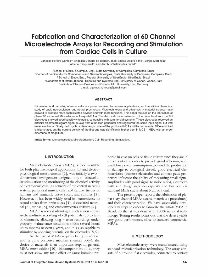
(a)
(b)
Figure 1. (a) Manufactured MEA; (b) MEA fabrication process at Center of Semiconductor Components and Nanotechnologies (UNICAMP). The fabrication process is subdivided into 5 steps: (I) deposition of an insulator interlayer between glass and conductor, (II) implementation of the electrodes, tracks and contact pads, (III) first insulation layer manufacturing, (IV) second insulation layer deposition, and (V) final components placement, such as ring and contact pins.
Fabrication and Characterization of 60 Channel Microelectrode Arrays for Recording and Stimulation from Cardiac Cells in CultureGomes; Barros; Destro-Filho; Martinoia; Pasquarelli & Swart
149Journal of Integrated Circuits and Systems 2016; v.11 / n.3:147-158
B. Step II
After cleaning and formation of the interlayer, next phase is electrode, track and contact pad produc-tion, by depositing a conductive material.
This step includes the lithography process in or-der to define electrodes, tracks, and contact pads, after sputtering deposition of the conductive material.
A wide variety of materials, such as nanocrys-talline diamond, gold, platinum (Pt), platinum – iri-dium alloy, tantalum, activated iridium oxide films (IrOx), electrically conducting polymer, poly(ethylene-dioxythiophene), graphene and titanium nitride (TiN) [17 – 19] can be applied in this step. Among these materials, titanium nitride shows low impedance, good biocompatibility, excellent stability and a large charge injection capacity (approximately 1 mCcm-2) which makes it a good option for devices that monitor and stimulate long – term biological activity with low noise [19, 20]. Thus, this material was chosen to compose the conductive parts of the MEA chip.
Electrodes are round and their diameters de-pend on the application and can vary widely, ranging from 10 µm to 160 micrometers [17]. However, sin-ce cell diameters for which this MEA is designed can reach 30 – 40 µm (neurons from dorsal root ganglion (DRG) from male Wistar rats) [21], the diameter of the electrodes of this work is 30 µm.
In addition to neurons in brain slices, in general, signal sources are within a radius of 30 µm around the electrode center and can be registered up to 100 mi-crometers [18], which is within range of a MEA elec-trode produced here, since the spacing is 200 µm. This distance is also sufficient to obtain a good resolution and sensitivity over the short period in which a release of adrenalin by chromaffin cells, neuroendocrine cells found in the medulla of the adrenal gland [18].
Lift – off was adopted to define the conductive region and 300 nm TiN layer with resistivity of 150 µΩ.cm was deposited by Sputtering.
C. Step III
In order to perform electrical measurements in liquid media, a passivation layer is required above con-ductive electrodes. This is a critical step during MEA development and usually employs silicon nitride, sili-con dioxide and silicon dioxide – silicon nitride – sili-con dioxide composite [10, 20, 17].
Capacitance (Cp) can be obtained through an expression that correlates the main parameters that in-fluence the amplitude of this variable, which is known as Sakurai – Tamary equation (Eq. 1) [17]:
(1)
Where ε0 is space permissivity, εr is insulating material permissivity, d is the thickness of the insulation layer, and L, W and t, are the length, width and thickness of the track, respectively.
Consequently, capacitance is determined by the material used in the insulation layer, its thickness, and geometric area of the track.
This process aims to prevent that the electroly-tes present in solution may infiltrate in this passivation layer, generating pin holes, and finally reaching the electrodes layer, effect that is not desired [17].
The definition of the insulating layer was made by lift – off process, with Sputtering deposition of 100 nm of silicon dioxide.
D. Step IV
Often, this single insulating silicon dioxide layer is not enough to block pin holes creation at the non – sensitive region of MEA, which could affect signal capture by electrodes. In order to avoid it, so the elec-trolyte can reach conductive surface from any direc-tion except openings (electrodes), it is appropriate to
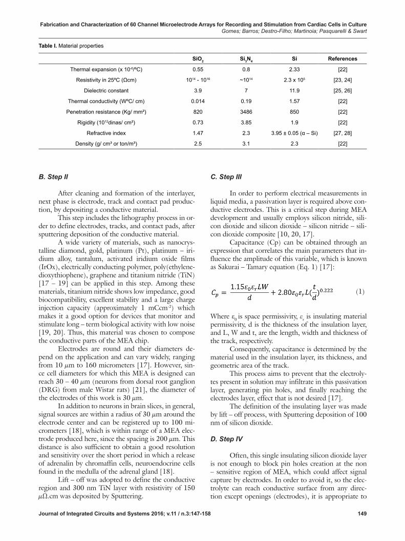
Table I. Material properties
SiO2 Si3N4 Si References
Thermal expansion (x 10-6/ºC) 0.55 0.8 2.33 [22]
Resistivity in 25ºC (Ωcm) 1014 - 1016 ~1014 2.3 x 10⁵ [23, 24]
Dielectric constant 3.9 7 11.9 [25, 26]
Thermal conductivity (WºC/ cm) 0.014 0.19 1.57 [22]
Penetration resistance (Kg/ mm²) 820 3486 850 [22]
Rigidity (1012dinas/ cm²) 0.73 3.85 1.9 [22]
Refractive index 1.47 2.3 3.95 ± 0.05 (α – Si) [27, 28]
Density (g/ cm³ or ton/m³) 2.5 3.1 2.3 [22]
Fabrication and Characterization of 60 Channel Microelectrode Arrays for Recording and Stimulation from Cardiac Cells in CultureGomes; Barros; Destro-Filho; Martinoia; Pasquarelli & Swart
150 Journal of Integrated Circuits and Systems 2016; v.11 / n.3:147-158
add another passivating layer that does not hinder the transparency of the device.
Therefore, the material chosen in this work was SU – 8 10 from MicroChem, a biocompatible and transparent material, with 7 µm thick.
E. Step V
Final step of MEA manufacturing requires the definition of a ring that surrounds the active region of MEA (i. e., electrodes zone), allowing to perform elec-trochemical measurements and to ensure that culture medium doesn’t evaporate too fast during cell experi-ments, keeping a sufficient volume of biological mate-rial [17]. For this purpose, a ring, which can hold up to about 800 µL solution [18], was made with glass. Rings had inner and outer diameters of 2.2cm and 2.6 cm, respectively, and they were fixed on the MEA sur-face with biocompatible glue.
III. RESULTS AND DISCUSSION
Electrical characterization was carry out at Cen-ter of Semiconductor Components and Nanotechno-logies at State
University of Campinas, University of Genoa and Universi-ty of Ulm. Tests were classified in: (A) analysis of the noise level (amplitude of the potential recorded with adding standard saline solution), (B) electrical stimulation, and (C) electrode test (cyclic vol-tammetry and impedance spectroscopy). These techni-ques are briefly described below, as well as the results obtained.
A. Noise Level
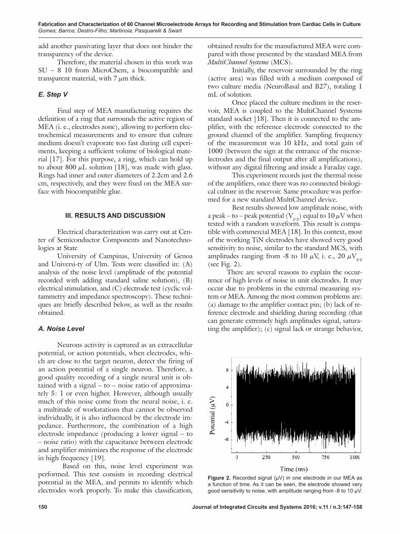
Neurons activity is captured as an extracellular potential, or action potentials, when electrodes, whi-ch are close to the target neuron, detect the firing of an action potential of a single neuron. Therefore, a good quality recording of a single neural unit is ob-tained with a signal – to – noise ratio of approxima-tely 5: 1 or even higher. However, although usually much of this noise come from the neural noise, i. e. a multitude of workstations that cannot be observed individually, it is also influenced by the electrode im-pedance. Furthermore, the combination of a high electrode impedance (producing a lower signal – to – noise ratio) with the capacitance between electrode and amplifier minimizes the response of the electrode in high frequency [19].
Based on this, noise level experiment was performed. This test consists in recording electrical potential in the MEA, and permits to identify which electrodes work properly. To make this classification,
obtained results for the manufactured MEA were com-pared with those presented by the standard MEA from MultiChannel Systems (MCS).
Initially, the reservoir surrounded by the ring (active area) was filled with a medium composed of two culture media (NeuroBasal and B27), totaling 1 mL of solution.
Once placed the culture medium in the reser-voir, MEA is coupled to the MultiChannel Systems standard socket [18]. Then it is connected to the am-plifier, with the reference electrode connected to the ground channel of the amplifier. Sampling frequency of the measurement was 10 kHz, and total gain of 1000 (between the sign at the entrance of the microe-lectrodes and the final output after all amplifications), without any digital filtering and inside a Faraday cage.
This experiment records just the thermal noise of the amplifiers, once there was no connected biologi-cal culture in the reservoir. Same procedure was perfor-med for a new standard MultiChannel device.
Best results showed low amplitude noise, with a peak – to – peak potential (Vp-p) equal to 10 µV when tested with a random waveform. This result is compa-tible with commercial MEA [18]. In this context, most of the working TiN electrodes have showed very good sensitivity to noise, similar to the standard MCS, with amplitudes ranging from -8 to 10 µV, i. e., 20 µVp-p (see Fig. 2).
There are several reasons to explain the occur-rence of high levels of noise in unit electrodes. It may occur due to problems in the external measuring sys-tem or MEA. Among the most common problems are: (a) damage to the amplifier contact pin; (b) lack of re-ference electrode and shielding during recording (that can generate extremely high amplitudes signal, satura-ting the amplifier); (c) signal lack or strange behavior,
Figure 2. Recorded signal (µV) in one electrode in our MEA as a function of time. As it can be seen, the electrode showed very good sensitivity to noise, with amplitude ranging from -8 to 10 µV.
Fabrication and Characterization of 60 Channel Microelectrode Arrays for Recording and Stimulation from Cardiac Cells in CultureGomes; Barros; Destro-Filho; Martinoia; Pasquarelli & Swart
151Journal of Integrated Circuits and Systems 2016; v.11 / n.3:147-158
which may occur by MEA use; (d) contact pads conta-mination (and this is a solvable problem because only a cleaning with pure alcohol is enough); and, finally, (e) irreversible damage to the electrode or contact pad. The latter can be observed from the coloring modifica-tion of the sensor [18].
Noise level comes both from amplification system and from MEA device. Regarding the device, signal amplitude depends on two factors. It is influen-ced by size and material that makes up the electrodes. The smaller the diameter of the electrode, the greater the noise.
For titanium nitride electrodes, which have a rough surface, impedance and noise are lower than those found in electrodes with same diameter made of other materials such as platinum. Initial noise can be higher of MEA is composed of hydrophobic materials and one way to solve this problem is to create a hy-drophilic surface, which is possible with the adoption of appropriate materials, such as titanium nitride [18].
To estimate the noise level contained in the recorded signal was obtained the RMS value for a non – defective microelectrode of our MEA. For the raw signal (unfiltered), the value found was 2.6 microvolts for the manufactured MEA. This result is satisfactory, since, to consider the microelectrode as functional, this parameter must be within the range of 2.5 to 8 micro-volts [18].
B. Electrical Stimulation Test
Electrical stimulation test evaluates the recor-ding ability of the electrodes and observes whether the output signal is similar to the input signal utilized to test.
Tested electrodes were the same which exhibi-ted good results in noise test. Other electrodes were disconnected.
Experimental setup in this experiment was si-milar to the setup described in section III – A, but in addition a cardiac signal was introduced in the culture medium. The signal tested in this case was an artificial electrocardiogram signal (ECG), which simulates real cardiac potential generated by cardiac cells. Therefore, it was injected an artificial ECG signal that consists of a peak – to – peak amplitude of 0.5mV with a cardiac cycle repetition frequency ranging from 3 to 23 Hz in the culture medium described in section III – A.
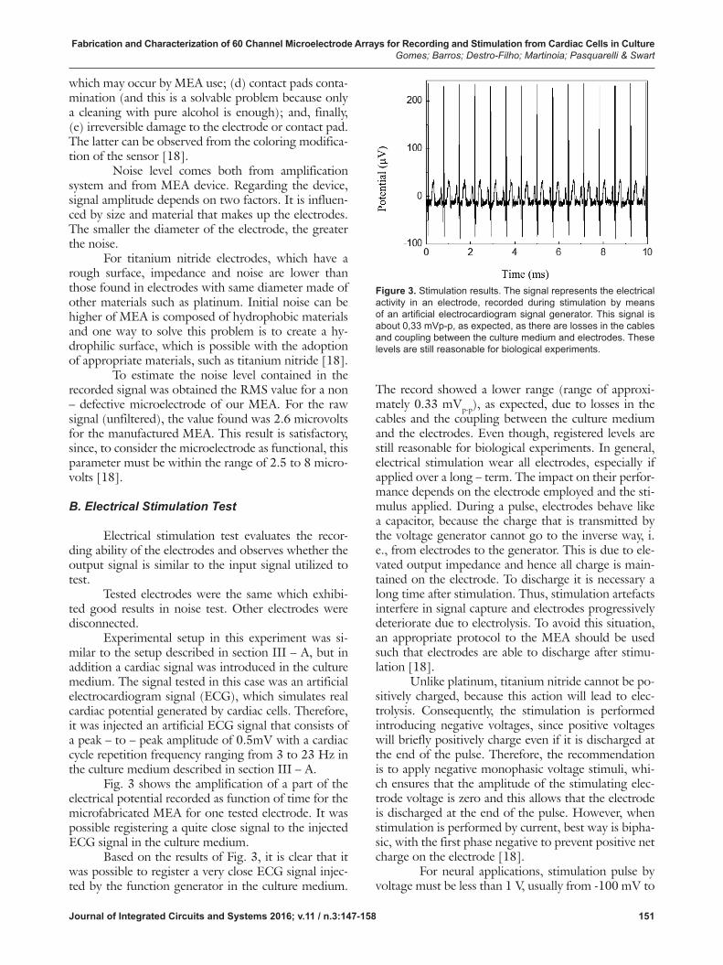
Fig. 3 shows the amplification of a part of the electrical potential recorded as function of time for the microfabricated MEA for one tested electrode. It was possible registering a quite close signal to the injected ECG signal in the culture medium.
Based on the results of Fig. 3, it is clear that it was possible to register a very close ECG signal injec-ted by the function generator in the culture medium.
The record showed a lower range (range of approxi-mately 0.33 mVp-p), as expected, due to losses in the cables and the coupling between the culture medium and the electrodes. Even though, registered levels are still reasonable for biological experiments. In general, electrical stimulation wear all electrodes, especially if applied over a long – term. The impact on their perfor-mance depends on the electrode employed and the sti-mulus applied. During a pulse, electrodes behave like a capacitor, because the charge that is transmitted by the voltage generator cannot go to the inverse way, i. e., from electrodes to the generator. This is due to ele-vated output impedance and hence all charge is main-tained on the electrode. To discharge it is necessary a long time after stimulation. Thus, stimulation artefacts interfere in signal capture and electrodes progressively deteriorate due to electrolysis. To avoid this situation, an appropriate protocol to the MEA should be used such that electrodes are able to discharge after stimu-lation [18].
Unlike platinum, titanium nitride cannot be po-sitively charged, because this action will lead to elec-trolysis. Consequently, the stimulation is performed introducing negative voltages, since positive voltages will briefly positively charge even if it is discharged at the end of the pulse. Therefore, the recommendation is to apply negative monophasic voltage stimuli, whi-ch ensures that the amplitude of the stimulating elec-trode voltage is zero and this allows that the electrode is discharged at the end of the pulse. However, when stimulation is performed by current, best way is bipha-sic, with the first phase negative to prevent positive net charge on the electrode [18].
For neural applications, stimulation pulse by voltage must be less than 1 V, usually from -100 mV to
Figure 3. Stimulation results. The signal represents the electrical activity in an electrode, recorded during stimulation by means of an artificial electrocardiogram signal generator. This signal is about 0,33 mVp-p, as expected, as there are losses in the cables and coupling between the culture medium and electrodes. These levels are still reasonable for biological experiments.
Fabrication and Characterization of 60 Channel Microelectrode Arrays for Recording and Stimulation from Cardiac Cells in CultureGomes; Barros; Destro-Filho; Martinoia; Pasquarelli & Swart
152 Journal of Integrated Circuits and Systems 2016; v.11 / n.3:147-158
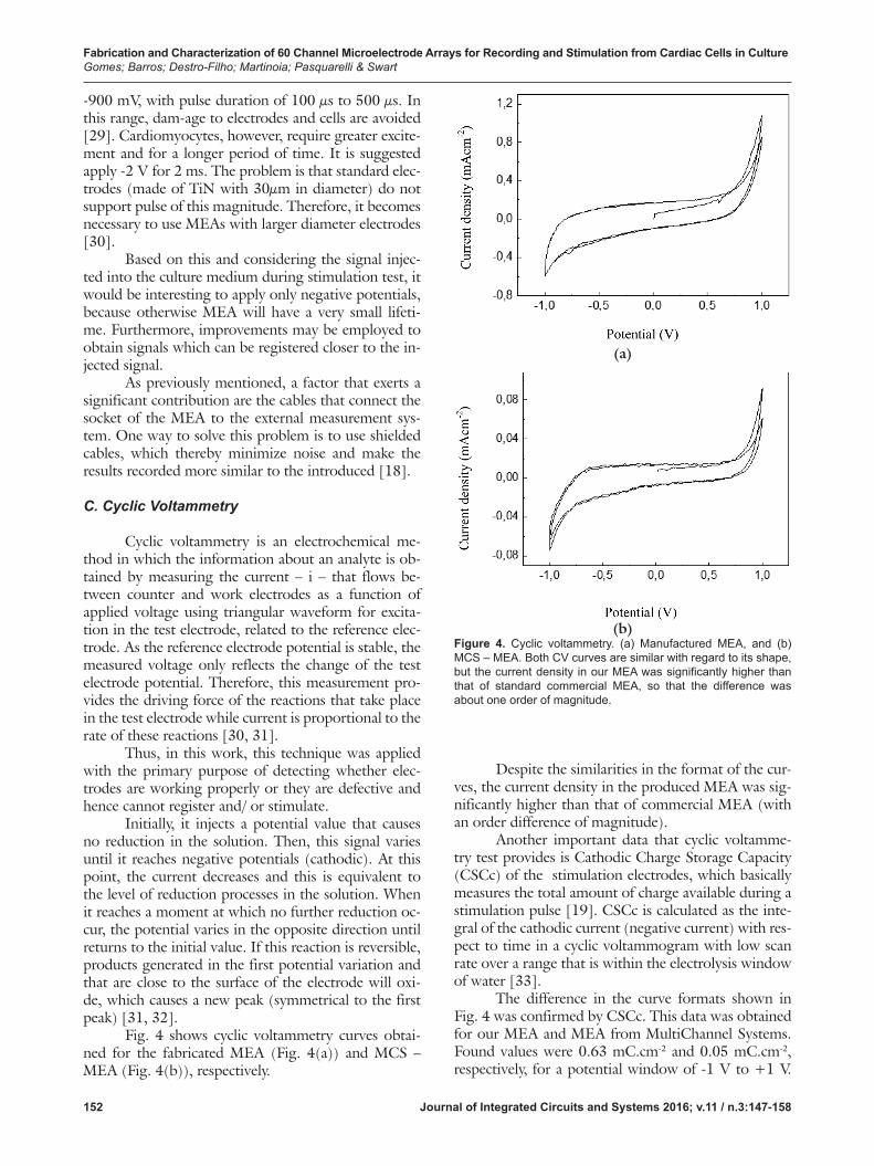
Despite the similarities in the format of the cur-ves, the current density in the produced MEA was sig-nificantly higher than that of commercial MEA (with an order difference of magnitude).
Another important data that cyclic voltamme-try test provides is Cathodic Charge Storage Capacity (CSCc) of the stimulation electrodes, which basically measures the total amount of charge available during a stimulation pulse [19]. CSCc is calculated as the inte-gral of the cathodic current (negative current) with res-pect to time in a cyclic voltammogram with low scan rate over a range that is within the electrolysis window of water [33].
The difference in the curve formats shown in Fig. 4 was confirmed by CSCc. This data was obtained for our MEA and MEA from MultiChannel Systems. Found values were 0.63 mC.cm-2 and 0.05 mC.cm-2, respectively, for a potential window of -1 V to +1 V.
-900 mV, with pulse duration of 100 µs to 500 µs. In this range, dam-age to electrodes and cells are avoided [29]. Cardiomyocytes, however, require greater excite-ment and for a longer period of time. It is suggested apply -2 V for 2 ms. The problem is that standard elec-trodes (made of TiN with 30µm in diameter) do not support pulse of this magnitude. Therefore, it becomes necessary to use MEAs with larger diameter electrodes [30].
Based on this and considering the signal injec-ted into the culture medium during stimulation test, it would be interesting to apply only negative potentials, because otherwise MEA will have a very small lifeti-me. Furthermore, improvements may be employed to obtain signals which can be registered closer to the in-jected signal.
As previously mentioned, a factor that exerts a significant contribution are the cables that connect the socket of the MEA to the external measurement sys-tem. One way to solve this problem is to use shielded cables, which thereby minimize noise and make the results recorded more similar to the introduced [18].
C. Cyclic Voltammetry
Cyclic voltammetry is an electrochemical me-thod in which the information about an analyte is ob-tained by measuring the current – i – that flows be-tween counter and work electrodes as a function of applied voltage using triangular waveform for excita-tion in the test electrode, related to the reference elec-trode. As the reference electrode potential is stable, the measured voltage only reflects the change of the test electrode potential. Therefore, this measurement pro-vides the driving force of the reactions that take place in the test electrode while current is proportional to the rate of these reactions [30, 31].
Thus, in this work, this technique was applied with the primary purpose of detecting whether elec-trodes are working properly or they are defective and hence cannot register and/ or stimulate.
Initially, it injects a potential value that causes no reduction in the solution. Then, this signal varies until it reaches negative potentials (cathodic). At this point, the current decreases and this is equivalent to the level of reduction processes in the solution. When it reaches a moment at which no further reduction oc-cur, the potential varies in the opposite direction until returns to the initial value. If this reaction is reversible, products generated in the first potential variation and that are close to the surface of the electrode will oxi-de, which causes a new peak (symmetrical to the first peak) [31, 32].
Fig. 4 shows cyclic voltammetry curves obtai-ned for the fabricated MEA (Fig. 4(a)) and MCS – MEA (Fig. 4(b)), respectively.
(a)
(b)Figure 4. Cyclic voltammetry. (a) Manufactured MEA, and (b) MCS – MEA. Both CV curves are similar with regard to its shape, but the current density in our MEA was significantly higher than that of standard commercial MEA, so that the difference was about one order of magnitude.
Fabrication and Characterization of 60 Channel Microelectrode Arrays for Recording and Stimulation from Cardiac Cells in CultureGomes; Barros; Destro-Filho; Martinoia; Pasquarelli & Swart
153Journal of Integrated Circuits and Systems 2016; v.11 / n.3:147-158
The difference in the results may be attributed mainly to the different thickness of the conductive layer, since both our MEA and MEA from MultiChannel Systems present electrodes with 30 µm in diameter made of titanium ni-tride, and with interelectrode distance of 200 µm.
Microelectrodes (with area smaller than 10,000 µm²) generally can show a charge density in a wide range varying from 0.2 to 3.5 mC.cm-2 [19]. Within the group of materials which operate via faradaic me-chanism, platinum/ platinum alloys, activated iridium oxide and thermal iridium oxide exhibit charge injec-tion limit ranging from 0.05 – 0.15 mC.cm-2, 1 – 5 mC.cm-2, and ~1 mC.cm-2, respectively, while in capa-citive materials, such as tantalum/ tantalum oxide and titanium nitride, these values were ~0.5 mC.cm-2, and ~1 mC.cm-2, respectively, with safe potential window of -0.9 V to +0.9 V [19]. However, charge injection li-mit was much higher. Values varied from 2.2 – 3.5mC.cm-2, at a potential window of -1 V to +1.2 V [34].
Although obtained charge injection threshold for TiN electrode by Cogan (2008) [19] is 1 mC.cm-2, CSC was 0.25 mC.cm-2. Calculated CSCc values by Weiland et al. (2002) [35] and Aryan et al. (2011) [36] were 0.55mC.cm-2, with potential window of -0.6 V to +0.8 V and 0.2mC.cm-2, with potential window of -1 V to +1 V, respectively.
Consequently, the values obtained for produced MEA in this work are within the expected range and are higher than those found in the studies cited. Fur-thermore, there is a plateau region in all TiN electro-des measured in the cathodic scanning phase (ranging from approximately -0.65 V to +0.65 V for our MEA and -0.61 V to +0.69 V for MEA from MultiChannel Systems). This behavior is present due to hydrogen ab-sorption that occurs before its release, which is similar to the cathodic reaction in platinum electrodes. After this interval there is an increase in the cathodic current and it represents therefore the evolution phase of gas hydrogen [34].
D. Impedance Spectroscopy
Another widely used technique for the elec-trical characterization of the MEA electrodes is Impe-dance Spectroscopy (IS), whose result allows setting whether an electrode is able to stimulate and record signals and, it is an interesting method for verifying in vivo. Moreover, it can also be used to study the tissues properties and electrical characteristics between elec-trode and solution interface [19, 36].
This technique works as follows: a unit frequen-cy sinusoidal excitation is applied (which may be by voltage or current) to the electrode and the resulting current in this given frequency is measured, allowing to obtain both electrical impedance and phase angle (real and imaginary parts of impedance).
A wide range of frequencies can be employed, being typically between <1 Hz and 105 Hz, with a small excitation magnitude so that current response versus voltage is obtained at each frequency. Excitation values can vary between ~10 mV and 50 mV [19].
In general, impedance is obtained with injec-tion of a small potential AC (alternating current) whi-ch can be, for example, a sinusoidal excitation in the electrochemical cell. Thus, the expression as a function of time is given by [37]:
(2)
Where Et and E0 are the potential at the time t and signal amplitude, with ω as radial frequency (radians/ second), which can be found as a function of frequen-cy f (in Hertz) as in Eq. 3 [37]:
(3)
Thus, the resulting signal (It) to a linear system has an amplitude I0 and is shifted in phase (Φ) as shown in Eq. 4 [37]:
(4)
Therefore, impedance (Z) as a function of the magnitude (Z0) and phase shift (Φ) can be found using a similar expression to the Ohm’s law. Then, [37]:
(5)
Most used forms to exhibit this result have been Bode diagram of the absolute value of Z (or |Z|) as a function of the frequency, and Nyquist diagram (ima-ginary component or capacitive impedance (Z’) as a function of the real component of the resistive impe-dance (Z)). It is interesting to note that in Nyquist diagram, each point means an impedance at a single frequency.
Related to an equivalent circuit modeling, al-though some electrochemical cells can present only one component, most cells employ elements that can be arranged in series and parallel.
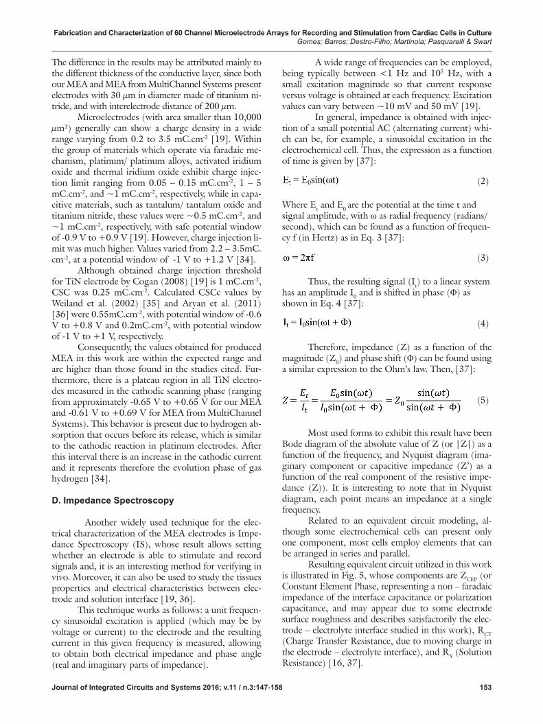
Resulting equivalent circuit utilized in this work is illustrated in Fig. 5, whose components are ZCEP (or Constant Element Phase, representing a non – faradaic impedance of the interface capacitance or polarization capacitance, and may appear due to some electrode surface roughness and describes satisfactorily the elec-trode – electrolyte interface studied in this work), RCT (Charge Transfer Resistance, due to moving charge in the electrode – electrolyte interface), and RS (Solution Resistance) [16, 37].
Fabrication and Characterization of 60 Channel Microelectrode Arrays for Recording and Stimulation from Cardiac Cells in CultureGomes; Barros; Destro-Filho; Martinoia; Pasquarelli & Swart
154 Journal of Integrated Circuits and Systems 2016; v.11 / n.3:147-158
Impedance ZCEP, which is the non – faradaic im-pedance resulting from the interface capacitance (pola-rization), is obtained using Eq. 6 [16]:
(6)
Where Q represents the magnitude of ZCEP, n, the hete-rogeneities on the surface (0 ≤ n ≤ 1, where n equal to 1 indicates a purely capacitive surface), and with ω = 2πf. The charge transfer solution resistances (resistance between working and reference electrodes) can be ob-tained by Eq. 7 and 8 [16]:
(7)
(8)
Where RT/ F = 26 mV at 298 K, J0 is the current mag-nitude flowing through electrode – electrolyte interfa-ce in the equilibrium situation (reduction current with the same module and direction opposite to oxidation), z is the number of electrons involved in the reduction – oxidation reaction, ρ is the solution resistivity (72 Ωcm for physiological saline) and r is the electrode radius [16].
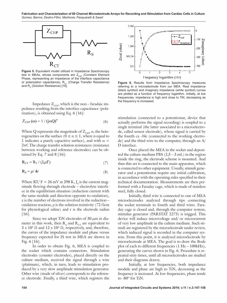
Since we adopt TiN electrodes of 30 µm in dia-meter in this work, then RS and RCT are equivalent to 3 x 10⁵ Ω and 12 x 10³ Ω, respectively, and, therefore, the curves of the impedance module and phase versus frequency expected for IS test in MEA are shown in Fig. 6 [16].
In order to obtain Fig. 6, MEA is coupled to the socket which contains connectors. Stimulation electrodes (counter electrodes), placed directly on the culture medium, received the signal through a wire (platinum), which, in turn, leads to stimulation pro-duced by a very slow amplitude stimulation generator. Other wire (made of silver) corresponds to the referen-ce electrode. Finally, a third wire, which registers the
stimulation (connected to a potentiostat, device that actually performs the signal recording) is coupled to a single terminal (the latter associated to a microelectro-de, called sensor electrode), whose signal is carried by the fourth ca –ble (connected to the working electro-de) and the third wire to the computer, through an A/ D interface.
Once placed the MEA in the socket and deposi-ted the culture medium PBS (2,5 – 3 mL) in the region inside the ring, the electrode scheme is mounted. And thus this set is connected to the main apparatus, which is connected to other equipment. Usually, stimuli gene-rator and a potentiostat require any initial calibration, in accordance with the operating rules specified in their technical documentation. Measurements are then per-formed with a Faraday cage, which is made of stainless steel, fully closed.
Initially, third wire is connected to one of MEA microelectrodes analyzed through tips connecting the socket terminals to fourth and third wires. Fara-day cage is closed and, through the computer system, stimulus generator (PARSTAT 2273) is trigged. This device will induce microvoltage and/ or microcurrent of very low amplitude in the culture medium. Such sti-muli are registered by the microelectrode under review, which induced signal is recorded in the computer sys-tem. From this point, it is analyzed microelectrode by microelectrode at MEA. The goal is to draw the Bode plot of each to different frequencies (1 Hz – 100kHz), generating the curves shown in Fig. 6. Procedure is re-peated sixty times, until all microelectrodes are studied and their diagrams drawn.
Initially, at low frequencies, both impedance module and phase are high to TiN, decreasing as the frequency is increased. At low frequencies, phase tends to -80º for TiN.
Figure 5. Equivalent model utilized in Impedance Spectroscopy test in MEAs, whose components are ZCEP (Constant Element Phase, representing an impedance of the interface capacitance or polarization capacitance), RCT (Charge Transfer Resistance) and RS (Solution Resistance) [16].
Figure 6. Results from Impedance Spectroscopy measures referring to a microelectrode from our MEA. Real impedance (black symbol) and imaginary impedance (white symbol) curves are plotted as a function of frequency logarithm. Initially, at low frequencies, impedance is high and close to TiN, decreasing as the frequency is increased.
Fabrication and Characterization of 60 Channel Microelectrode Arrays for Recording and Stimulation from Cardiac Cells in CultureGomes; Barros; Destro-Filho; Martinoia; Pasquarelli & Swart
155Journal of Integrated Circuits and Systems 2016; v.11 / n.3:147-158
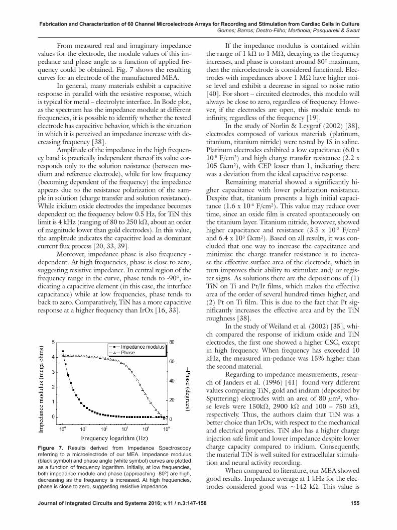
From measured real and imaginary impedance values for the electrode, the module values of this im-pedance and phase angle as a function of applied fre-quency could be obtained. Fig. 7 shows the resulting curves for an electrode of the manufactured MEA.
In general, many materials exhibit a capacitive response in parallel with the resistive response, which is typical for metal – electrolyte interface. In Bode plot, as the spectrum has the impedance module at different frequencies, it is possible to identify whether the tested electrode has capacitive behavior, which is the situation in which it is perceived an impedance increase with de-creasing frequency [38].
Amplitude of the impedance in the high frequen-cy band is practically independent thereof its value cor-responds only to the solution resistance (between me-dium and reference electrode), while for low frequency (becoming dependent of the frequency) the impedance appears due to the resistance polarization of the sam-ple in solution (charge transfer and solution resistance). While iridium oxide electrodes the impedance becomes dependent on the frequency below 0.5 Hz, for TiN this limit is 4 kHz (ranging of 80 to 250 kΩ, about an order of magnitude lower than gold electrodes). In this value, the amplitude indicates the capacitive load as dominant current flux process [20, 33, 39].
Moreover, impedance phase is also frequency - dependent. At high frequencies, phase is close to zero, suggesting resistive impedance. In central region of the frequency range in the curve, phase tends to -90º, in-dicating a capacitive element (in this case, the interface capacitance) while at low frequencies, phase tends to back to zero. Comparatively, TiN has a more capacitive response at a higher frequency than IrOx [16, 33].
If the impedance modulus is contained within the range of 1 kΩ to 1 MΩ, decaying as the frequency increases, and phase is constant around 80º maximum, then the microelectrode is considered functional. Elec-trodes with impedances above 1 MΩ have higher noi-se level and exhibit a decrease in signal to noise ratio [40]. For short – circuited electrodes, this modulo will always be close to zero, regardless of frequency. Howe-ver, if the electrodes are open, this module tends to infinity, regardless of the frequency [19].
In the study of Norlin & Leygraf (2002) [38], electrodes composed of various materials (platinum, titanium, titanium nitride) were tested by IS in saline. Platinum electrodes exhibited a low capacitance (6.0 x 10⁻⁵ F/cm²) and high charge transfer resistance (2.2 x 10⁵ Ωcm²), with CEP lesser than 1, indicating there was a deviation from the ideal capacitive response.
Remaining material showed a significantly hi-gher capacitance with lower polarization resistance. Despite that, titanium presents a high initial capaci-tance (1.6 x 10⁻⁴ F/cm²). This value may reduce over time, since an oxide film is created spontaneously on the titanium layer. Titanium nitride, however, showed higher capacitance and resistance (3.5 x 10⁻² F/cm² and 6.4 x 10³ Ωcm²). Based on all results, it was con-cluded that one way to increase the capacitance and minimize the charge transfer resistance is to increa-se the effective surface area of the electrode, which in turn improves their ability to stimulate and/ or regis-ter signs. As solutions there are the depositions of (1) TiN on Ti and Pt/Ir films, which makes the effective area of the order of several hundred times higher, and (2) Pt on Ti film. This is due to the fact that Pt sig-nificantly increases the effective area and by the TiN roughness [38].
In the study of Weiland et al. (2002) [35], whi-ch compared the response of iridium oxide and TiN electrodes, the first one showed a higher CSC, except in high frequency. When frequency has exceeded 10 kHz, the measured im-pedance was 15% higher than the second material.
Regarding to impedance measurements, resear-ch of Janders et al. (1996) [41] found very different values comparing TiN, gold and iridium (deposited by Sputtering) electrodes with an area of 80 µm², who-se levels were 150kΩ, 2900 kΩ and 100 – 750 kΩ, respectively. Thus, the authors claim that TiN was a better choice than IrOx, with respect to the mechanical and electrical properties. TiN also has a higher charge injection safe limit and lower impedance despite lower charge capacity compared to iridium. Consequently, the material TiN is well suited for extracellular stimula-tion and neural activity recording.
When compared to literature, our MEA showed good results. Impedance average at 1 kHz for the elec-trodes considered good was ~142 kΩ. This value is
Figure 7. Results derived from Impedance Spectroscopy referring to a microelectrode of our MEA. Impedance modulus (black symbol) and phase angle (white symbol) curves are plotted as a function of frequency logarithm. Initially, at low frequencies, both impedance module and phase (approaching -80º) are high, decreasing as the frequency is increased. At high frequencies, phase is close to zero, suggesting resistive impedance.
Fabrication and Characterization of 60 Channel Microelectrode Arrays for Recording and Stimulation from Cardiac Cells in CultureGomes; Barros; Destro-Filho; Martinoia; Pasquarelli & Swart
156 Journal of Integrated Circuits and Systems 2016; v.11 / n.3:147-158
close to the range obtained by Egert et al. (1998) [20]. With TiN electrodes of the same diameter, they were able to measure impedance ranging from 80 to 250 kΩ, whose magnitude is about an order of magnitude smaller than the impedance seen in planar gold elec-trodes. Furthermore, for our device, results are very close to those found for impedance spectroscopy at the MEA from MultiChannel Systems, which shows impe-dance values in the range of 30 – 400 kΩ.
Comparing our results to the literature, the main contribution of this work is focused in the MEA fabrication, which was fully manufactured in Brazil employing 100% of local technology, as follows.
a) Insulation layer
In the literature, MEAs are often passivated with silicon– based materials, such as SiO2 [42 – 44], Si3N4 [20, 45, 46], and SiO2 – Si3N4 – SiO2 composite [10, 17], involving thickness up to 100 nm. In order to accomplish this task, this insulation material must be fully capacitive, so there is no leakage current or any other conductivity clue [10]. According to (1), the thickness of the material used in the insulation layer does influence this capacitance. Thus, in order to achie-ve a suitable insulation, a thicker layer is desirable [17, 47, 48]. In this context, a possible option is to employ polymers (such as polyimide, SU – 8), that can be im-plemented with up to several micrometers of thickness, and consists of photosensitive materials. In consequen-ce, this enables simple and low cost patterning. The-refore, in order to ensure proper insulation, instead of using a single thick layer based on SiO2, we decided to use two layers: SiO2 and SU – 8. Among the advanta-ges of the latter, we can highlight its transparency, high chemical stability and biocompatibility [10, 49, 50].
b) Interlayer
We have performed a step that is not present in most studies [10, 36, 51]: the interlayer, which we consider mandatory in order to implement an efficient device. The presence of this layer on MEA will assure that possible contaminants arising from the substrate are minimized, therefore avoiding the damage of the culture plated on the MEA, as well as improving the adhesion between substrate and conductive layer.
IV. CONCLUSIONS
This paper presented the production and cha-racterization of 60 – channel MEAs, with TiN microe-lectrodes on glass substrate and insulation of SiO2 and SU – 8, for use in neural cell cultures, completely ma-nufactured in Brazil.
Experimental analysis pointed out that our MEA yields very good performance. Best electro-des in our MEA presented very good sensitivity to noise, leading to amplitudes of 10µVp-p, with RMS value of 2.6 µV. During stimulation test, signals re-corded at microelectrodes yielded a waveform very close to the ECG injected by the function generator, but with lower amplitude (which is expected). In addition, regarding the Cyclic Voltammetry, resul-ting curves of our MEA presented similar shapes to the commercial device, but with higher current density (about an order of magnitude higher), with high CSCc amplitude (0.63 mC.cm-2, with a po-tential window of –1 V to +1 V), which may be considered a reasonable result. Finally, Impedance Spectroscopy depicted that the impedance of our electrodes (~41kΩ at 1 kHz) is very close to those found in commercial devices. Moreover, due to the qualities of the conductor used (such as high charge injection safe limit and low impedance), TiN may be considered an interesting, adequate option for extracellular stimulation and neural activity recor-ding.
Hence, based on all these tests and considera-tions, we can conclude that we have successfully deve-loped both masks and process steps, as in the imple-mentation of MEAs with functional microelectrodes. Results arising from testing the device reported in this work are within the expected range and compatible to standard commercial MEAs, so they are suitable for MEA applications.
ACKNOWLEDGEMENTS
The authors would like to acknowledge the fi-nancial support from Coordenação de Aperfeiçoamen-to de Pessoal de Nível Superior (CAPES) Brazilian foundation and from INCT/ CNPq – NAMITEC. We are also grateful to the Instituto de Física ‘GlebWata-ghin’ (IFGW), in State University of Campinas, for the manufacture of glass rings, and G. Almeida (CTI – Campinas) for the patterning of designed masks on a glass mask with chromium and to A. Flacker for clea-ning the glass substrates.
REFERENCES
[1] M. Chiappalone, A. Vato. M. B. Tedesco, M. Marcoli, F. Da-vide, and S. Martinoia, “Networks of neurons coupled to mi-croelectrode arrays: a neuronal sensory system for pharma-cological applications.,” Bionsen. Bioelectron., vol. 18, no. 5 – 6, May, 2003, pp. 627 – 634.
[2] W. B. F. Rieke, D. Warland, R. R. van Steveninck, Spikes: exploring the neural code, Cambridge, MA: The MIT Press, 1997, pp. 234.
Fabrication and Characterization of 60 Channel Microelectrode Arrays for Recording and Stimulation from Cardiac Cells in CultureGomes; Barros; Destro-Filho; Martinoia; Pasquarelli & Swart
157Journal of Integrated Circuits and Systems 2016; v.11 / n.3:147-158
[3] S. Martinoia, L. Bonzano, M. Chappalone, and M. Tedesco, “Electrophysiological activity modulation by chemical stimu-lation in networks of cortical neurons coupled to microelec-trode arrays: a biosensor for neuropharmacological applica-tions,” Sensors Actuators B Chem., vol. 18, no. 1 – 2, Jul., 2005, pp. 589 – 596.
[4] R. E. Hampson, J. D. Simeral, and S. A. Deadwyler, “Distribu-tion of spatial and nonspatial information in dorsal hippocam-pus,” Nature, vol. 402, no. 6762, Dec., 1999, pp. 610 – 614.
[5] R. Madhavan, Z. C. Chao, and S. M. Potter, “Plasticity of re-curring spatiotemporal activity patterns in cortical networks,” Phys. Biol., vol. 4, no. 3, Sep., 2007, pp. 181 – 193.
[6] C. L. Torborg, K. A. Hansen, and M. B. Feller, “High frequen-cy, synchronized bursting drives eye – specific segregation of retino - geniculate projections,” Nat. Neurosci., vol. 8, no. 1, Jan., 2005, pp. 72 – 78.
[7] P. A. Friedmann, “Novel mapping techniques for cardiac electrophysiology,” Heart, vol. 87, no. 6, Jun., 2002, pp. 575 – 582.
[8] S. M. Potter and T. B. DeMarse, “A new approach to neural cell culture for long – term studies,” J. Neurosci. Methods, vol. 110, no. 1 – 2, Sep., 2001, pp. 17 – 24.
[9] Y. H. Tennico, M. T. Koesdjojo, S. Kondo, D. T. Mandrell, and V. T. Remcho, “Surface modification – assisted bonding of polymer – based microfluidic devices,” Sensors Actuators B. Chem., vol. 143, no. 2, Jan., 2010, pp 799 – 804.
[10] M O. Heuschkel, C. Wirth, E. Steidl, and B. Buisson, “Devel-opment of 3D multielectrode arrays for use with acute tissue slices,” in Advances in network electrophysiology using mul-tielectrode arrays, M. Taketani; M. Baudry, Ed. New York, NY: Springer Science+Business Media, Inc., 2006, pp. 69 – 111.
[11] D. A. Borkholder, J. Bao, N. I. Maluf, E. R. Perl, and G. T. Kovacs, “Microelectrode arrays for stimulation of neural slice preparations,” J. Neurosci. Methods, vol. 77, no. 1, Nov., 1997, pp. 61 – 66.
[12] Q. Dai, R. Rajasekharan, H. Butt, K. Won, X. Wang, T. D. Wilkinson, and G. Amaragtunga, “Transparent liquid – crys-tal – based microlens arrays using vertically aligned carbon nanofiber electrodes on quartz substrates,” Nanotechnology, vol. 22, no. 11, Mar., 2011, pp. 115 – 201.
[13] S. A. Boppart, B. C. Wheeler, and C. S. Wallace, “A flexible perforated microelectrode array for extended neural record-ings,” IEEE Trans. Biomed. Eng., vol. 39, no. 1, Jan., 1992, pp. 37 – 42.
[14] S. Khan, A. Mian, and G. Newaz, Thin films and coatings in biology, S. Nazarpour, Ed. Dordrecht, Springer: 2013, pp. 301 – 330.
[15] A. Hai, J. Shappir, and E. Spira. “Long-term, multisite, paral-lel, in-cell recording and stimulation by an array of extrace-lular microelectrodes,” J Neurophysiol., vol. 104, 2010, pp. 559 – 568.
[16] W. Franks, I. Schenker, P. Schmutz, and A. Hierlemann, “Im-pedance characterization and modeling of electrodes for biomedical applications,” IEEE Trans. Biomed. Eng., vol. 52, no. 7, Jul., 2005, pp. 1295 – 1302.
[17] K. Wang, “A carbon nanotube microelectrode array for neural stimulation,” Stanford University, 2006.
[18] M. Systems, “Microelectrode array (MEA) manual,” Reutlin-gen, 2015, pp. 1 – 131.
[19] S. F. Cogan, “Neural stimulation and recording electrodes,” Annu.Rev. Biomed. Eng., vol. 10, Jan., 2008, pp. 275 – 309.
[20] U. Egert, B. Schlosshauer, S. Fennrich, W. Nisch, M. Fejtl, T. Knott, T. Müller, and H. Hämmerle, “A novel organotypic long – term culture of the rat hippocampus on substrate – integrated multielectrode arrays,” Brain Res. Protoc., vol. 2, no. 4, Jun., 1998, pp. 229 – 242.
[21] M. Martínez-Gutiérrez, and J. E. Castellanos, “Morphological and biochemical characterisation of sensory neurons infec-ted in vitro with rabies virus,” Acta Neuropathol., vol. 114, 2007, pp. 263 – 269.
[22] K. E. Petersen, “Silicon as a mechanical material,” in ProceeP-dings of the IEEE, 1982, pp. 420 – 434.
[23] S. M. Sze and K. K. Ng, Physics of semiconductor devices, 3rd ed. Hoboken, NJ: John Wiley & Sons, 2007, pp. 1 – 814.
[24] S. Wolf, Silicon processing for the VLSI era – Vol. 2: Process integration, Sunset Beach, CA: Lattice Press, 1990, pp. 1 – 782.
[25] J. Robertson, “High dielectric constant oxides,” Eur. Phys. J. Appl. Phys., vol. 28, 2004, pp. 265 – 291.
[26] O. Toader, and S. John, “Proposed square spiral microfa-brication architecture for large three – dimensional photonic band gap crystals,” Science, vol. 292, no. 5519, 2001, pp. 1133 – 1135.
[27] R. Machorro, E. C. Samano, G. Soto, F. Villa, and L. Costa – Araiza, “Modification of refractive index in silicone oxynitride films during deposition,” Materials Letters, vol. 45, 2000, pp. 47 – 50.
[28] J. Bergmann, M. Heusinger, G. Andrä, and F. Falk, “Tempe-rature dependente optical properties of amorphous silicone for diode laser crystallization,” Optics Express, vol. 20, no. 106, 2012, pp. A856 – A863.
[29] S. M. Potter, D. A. Wagenaar, and T. B. DeMarse, “Closing the loop: stimulation feedback systems for embodied MEA cultures,” in Advances in network electrophysiology: using multielectrode arrays, M. Taketani, M. Baudry, Ed. New York, NY: Springer Science+Business Media, Inc., 2006, pp. 215 – 242.
[30] D. A. Wagenaar, R. Madhavan, J. Pine, and S. M. Potter, “Controlling bursting in cortical cultures with closed – loop multielectrode stimulation,” J. Neurosci., vol. 25, no. 3, Jan., 2005, pp. 680 – 688.
[31] M. J. Madou, “Electrochemical and optical analytical tech-niques,” in Solid – state physics, fluidics, and analytical tech-niques in micro and nanotechnology, vol. 1, Irvine, CA: CRC Press, 2011, pp. 552 – 555.
[32] C. G. Zoski, “Handbook of electrochemistry,” Oxford, UK: ElU-sevier, 2007.
[33] W. Hasenkamp, S. Musa, A. Alexandru, W. Eberle, and C. Bartic, “Electrodeposition and characterization of iridium oxi-de as electrode material for neural recording and stimula-tion,” in World Congress on Medical Physics and Biomedical Engineering, 2009, pp. 472 – 475.
[34] D. M. Zhou and R. J. Greenberg, “Electrochemical charac-terization of titanium nitride microelectrode arrays for charge – injection applications,” in 25th Annual International Confer-ence of the IEEE EMBS, 2003, pp. 1964 – 1967.
[35] J. D. Weiland, D. J. Anderson, and M. S. Humayun, “In vitro electrical properties for iridium oxide versus titanium nitride stimulating electrodes,” IEE Trans. Biomed. Eng., vol. 49, no. 12, Dec., 2002, pp. 1574 – 1579.
[36] N. P. Aryan, M. Imam, H. Bin, C. Brendler, S. Kibbel, G. Heu-sel, and A. Rothermel, “In vitro study of titanium nitride elec-trodes for neural stimulation,” in 33rd Annual International Conference of the IEEE EMBS, 2011, pp. 2866 – 2869.
Fabrication and Characterization of 60 Channel Microelectrode Arrays for Recording and Stimulation from Cardiac Cells in CultureGomes; Barros; Destro-Filho; Martinoia; Pasquarelli & Swart
158 Journal of Integrated Circuits and Systems 2016; v.11 / n.3:147-158
[37] A. J. Bard, and L. R. Faulkner, “Techniques based on cono-cepts of impedance,” in Electrochemical methods: Funda-mentals and applications. New York, NY: John Wiley & Sons, Inc., 2001, pp. 368 – 416.
[38] A. Norlin, J. Pan, and C. Leygraf, “Investigation of interfacial capacitance of Pt, Ti and TiN coated electrodes by electro-chemical impedance spectroscopy,” Biomol. Eng., vol. 19, 2002, pp. 67 – 71.
[39] F. Heer, W. Franks, A. Blau, S. Taschini, C. Ziegler, A. Hier-lemann, and H. Balter, “CMOS microelectrode array for the monitoring of electrogenic cells,” Biosens. Bioelectron., vol. 20, 2004, pp. 358 – 366.
[40] M. O. Heuschkel, M. Fejtl, M. Raggenbass, D. Bertrand, and P. Renaud, “A three – dimensional multi – electrode array for multisite stimulation and recording in acute brain slices,” J. Neurosci. Methods, vol. 114, no. 2, Marc., 2002, pp. 135 – 148.
[41] M. Janders, U. Egert, M. Stelzle, and W. Nisch, “Novel thin film titanium nitride microelectrodes with excellent charge transfer capability for cell stimulation and sensing applica-tions,” in 18th Annual International Conference of the IEEE Engineering in Medicine and Biology Society, 1996, pp. 245 – 247.
[42] R. Kim, S. Joo, H. Jung, N. Hong, and Y. Nam, “Recent trends in microelectrode array technology for in vitro neural interface platform,” Biomed. Eng. Lett., vol. 4, 2014, pp. 129 – 141.
[43] A. Blau, Prospects for neuroprosthetics: Flexible microelec-trode arrays with polymer conductors, in Applied Biomedical Engineering, G. D. Gargiulo, and A. McEwan (Ed.), ISBN: 978 – 953 – 307 – 256 – 2, InTech: 2011, pp. 83 – 123.
[44] R. Kiran, L. Rousseau, G. Lissorgues, E. Scorsone, A. Bon-grain, B. Yvert, S. Picaud, P. Mailley, and P. Bergonzo, “Mul-tichannel boron doped nanocrystalline diamond ultramicro-electrode arrays: Design, fabrication and characterization,” Sensors, vol. 12, 2012, pp. 7669 – 7681.
[45] H. Charkhkar, G. L. Knaack, B. E. Gnade, E. W. Keeder, J. J. Pancrazio, “Development and demonstration of a dispos-able low – cost microelectrode array for cultured neuronal network recording,” Sensors and Actuators B., vol. 161, Nov. 2011, pp. 655 – 660.
[46] K. C. Cheung, K. Djupsund, Y. Dan, and L. P. Lee, “Implant-able multichannel electrode array based on SOI technology,” Journal of Microelectromechanical Systems, vol. 12, no. 2, April 2003, pp. 179 – 184.
[47] A. M. H. Ng, Y. Wang, W. C. Lee, C. T. Lim, K. P. Loh, and H. Y. Low, “Patterning of graphene with tunable size and shape for microelectrode array devices,” Carbon, vol. 67, 2014, pp. 390 – 397.
[48] C. A. Rusinek, M. F. Becker, R. Rechenber, and T. Schuelke, “Fabrication and characterization of boron doped diamond microelectrode arrays of varied geometry,” Electrochemistry Communications, vol. 73, 2016, pp. 10 – 14.
[49] G. Márton, G. Orbán, M. Kiss, A. Pongrácz, and I. Ulbert, “A novel polyimide – platinum – SU-8 microelectrode array for various electrophysiological applications,” Procedia En-gineering, in Eurosensors 2014, the 28th European Confer-ence on Solid – State Transducers, vol. 87, 2014, pp. 380 – 383.
[50] L. Berdondini, M. Chiappalone, P. D. van der Wal, K. Imfeld, N. F. de Rooij, M. Koudelka – Hep, M. Tedesco, S. Martinoia, J van Pelt, G. Le Masson, and A. Garenne, “A microelectrode array (MEA) integrated with clustering structures for investi-gating in vitro neurodynamics in confined interconnected sub – populations of neurons,” Sensors and Actuators B: Chemi-cal, vol. 14, no. 1, March 2006, pp. 530 – 541.
[51] A. Czeschik, A. Offenhäusser, and B. Wolfrum, “Fabrication of MEA – based nanocavity sensor arrays for extracellular recording of action potentials,” Phys. Status Solidi.A, vol.211, no. 6, 2014, pp. 1462 – 1466.