polymer self assembly for electronic devices
TRANSCRIPT

Polymer Self Assembly for Electronic Devices
C. T. Black Group Leader, Electronic Materials Center for Functional Nanomaterials Brookhaven National Laboratory [email protected]
BNL-95199-2011-CP

1996-2006: IBM T. J. Watson Research Center
Self assembly for high-performance semiconductor microelectronics
2006- Brookhaven National Laboratory
Nanostructured devices for energy conversion

cylindrical lamellar
PMMA
polystyrene (PS)
Self-assembled block copolymer films T. P. Russell, M. T. Tuominen (UMass Amherst), C. J. Hawker (IBM) Adv. Mat., 12, 787 (2000).
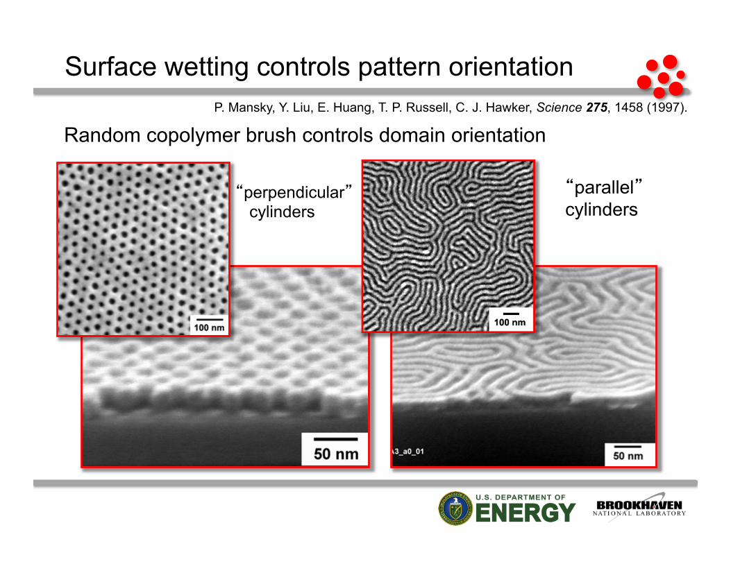
Surface wetting controls pattern orientation
“perpendicular” cylinders
“parallel” cylinders
Random copolymer brush controls domain orientation P. Mansky, Y. Liu, E. Huang, T. P. Russell, C. J. Hawker, Science 275, 1458 (1997).

• Large area patterning (~cm2) • Small feature sizes (<20nm) • High feature density (>1010/cm2) • Periodic structures (<40nm pitch) • Reasonable size uniformity
(σ~10%); little uniformity in ordering
• Dimensions (somewhat) tunable • Materials are semiconductor
process compatible • Process tooling already in
existing manufacturing infrastructure
Polymer self assembly for device fabrication
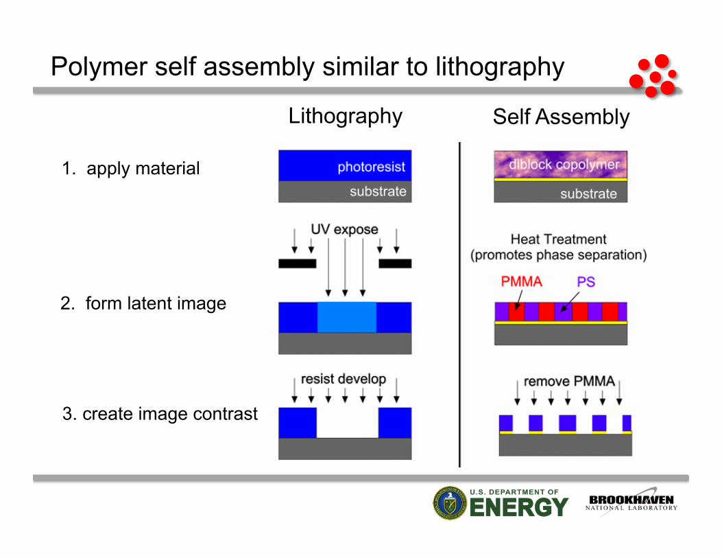
Polymer self assembly similar to lithography
1. apply material
2. form latent image
3. create image contrast
Lithography Self Assembly
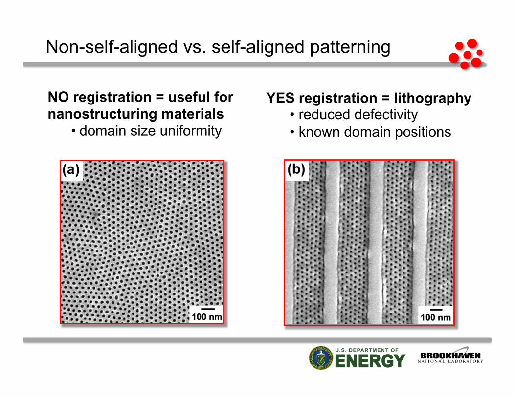
Non-self-aligned vs. self-aligned patterning
NO registration = useful for nanostructuring materials
• domain size uniformity
YES registration = lithography • reduced defectivity • known domain positions

Block copolymer lithography
Amazing recent advances: Massachusetts Institute of Technology Caroline Ross, Karl Berggren Hitachi Global Storage Technologies
Ricardo Ruiz, with Paul Nealey (Univ. Wisconsin)
IBM Almaden Research Center
Joy Cheng

Some lithography requirements questions
How scalable is block copolymer self assembly? What are ultimate limits on size, pitch?
How smooth are the self-assembled pattern features?
targets (ITRS): CD: 3σ= 2.3nm; LWR: 3σ= 1.2nm Can we create/integrate robust fabrication processes?
pattern formation pattern develop plasma etch resistance
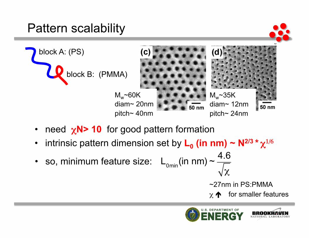
Pattern scalability
block B: (PMMA)
block A: (PS)
• need χN> 10 for good pattern formation • intrinsic pattern dimension set by L0 (in nm) ~ N2/3 * χ1/6
• so, minimum feature size:
~27nm in PS:PMMA χ é for smaller features
Mw~60K diam~ 20nm pitch~ 40nm
Mw~35K diam~ 12nm pitch~ 24nm
L0min(in nm) ~ 4.6!

Pattern feature roughness
!
"(in nm) ~ 26#
block interface width set by:
~4nm in PS:PMMA spheres cylinders" lamellae"Need χé for sharper interfaces But, need interdiffusion (χ ê) to heal defects
(?: Lamellae are always smoother than cylinders)

Pattern feature roughness
!
"(in nm) ~ 26#
block interface width set by:
~4nm in PS:PMMA
use T-dependence of χ to control Δ and heal defects
χ ~ A + B/T
e.g., GOOD: PS-b-P2VP: strong T-dependence of χ NOT-SO-GOOD: PS-b-PMMA: little T-dependence
See, for example, Hammond, Kramer, et al., Macromolecules 38, 6575 (2005).

as formed (no develop) PS and PMMA present
UV exp.+ liquid develop PMMA removed; some collapse
O2 plasma develop PMMA removed; lose PS
Pattern develop
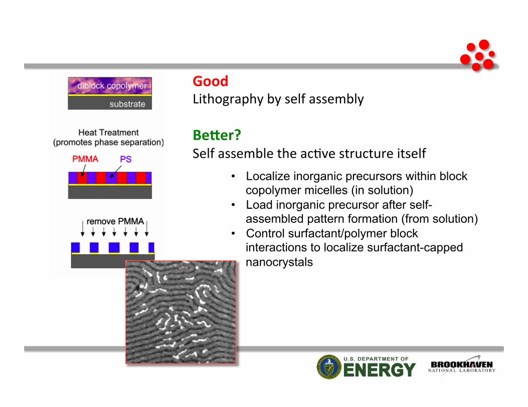
Good Lithography by self assembly
Be'er? Self assemble the ac4ve structure itself
• Localize inorganic precursors within block copolymer micelles (in solution)
• Load inorganic precursor after self-assembled pattern formation (from solution)
• Control surfactant/polymer block interactions to localize surfactant-capped nanocrystals
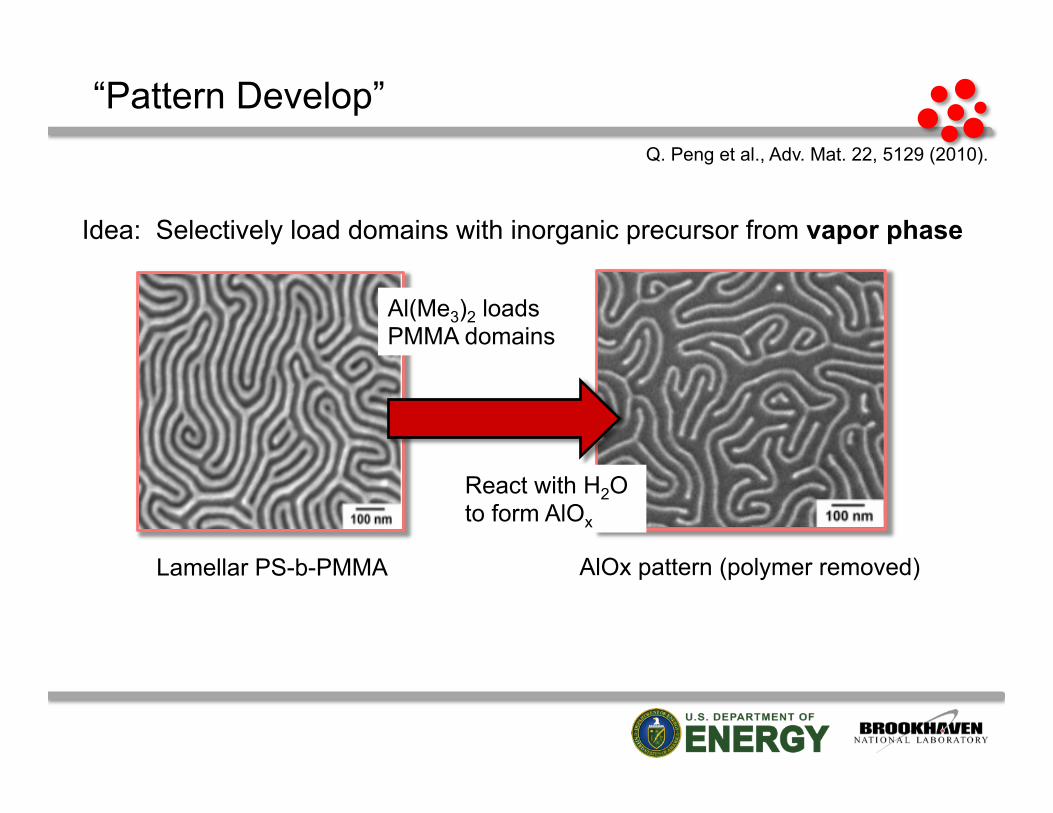
Q. Peng et al., Adv. Mat. 22, 5129 (2010).
Idea: Selectively load domains with inorganic precursor from vapor phase
“Pattern Develop”
Lamellar PS-b-PMMA AlOx pattern (polymer removed)
Al(Me3)2 loads PMMA domains
React with H2O to form AlOx

Plasma etch resistance
Converting PMMA domains to AlOx: • prevents resist collapse during “develop” • increases plasma etch resistance
AlOx pattern (polymer removed)
Etched silicon grating
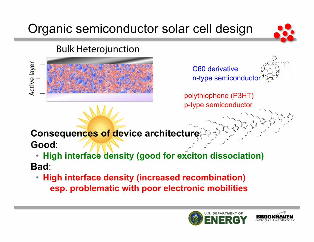
Organic semiconductor solar cell design
Consequences of device architecture: Good:
• High interface density (good for exciton dissociation) Bad:
• High interface density (increased recombination) esp. problematic with poor electronic mobilities
polythiophene (P3HT) p-type semiconductor
C60 derivative n-type semiconductor

P3HT structure and electronic properties
P3HT has “good” mobility perpendicular to lamellar stacking
P3HT has poor mobility along lamellar stacking direction
Regioregular polythiophene (P3HT) is a semi-crystalline polymer
π-π stacking
lamellar stacking
µh ≈ 0.1 cm2V-1s-1
µh ≈ 0.0001 cm2V-1s-1
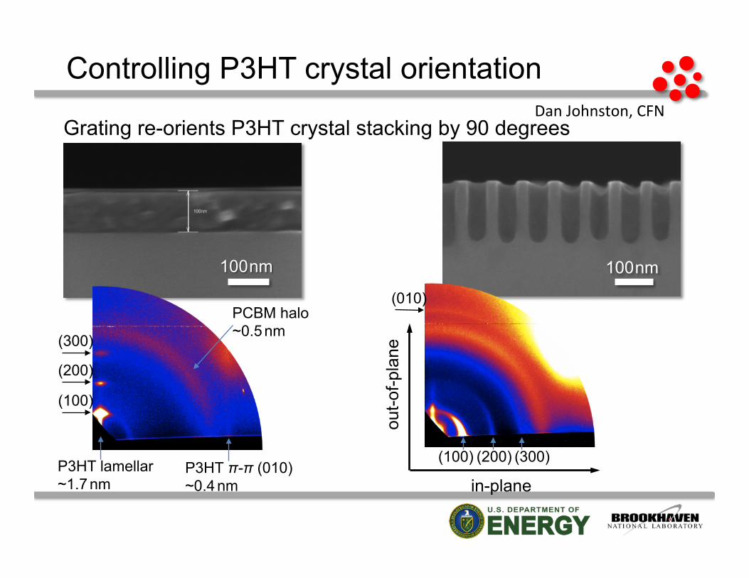
P3HT lamellar ~1.7 nm
(300)
(200)
(100)
P3HT π-π (010) ~0.4 nm
in-plane ou
t-of-p
lane
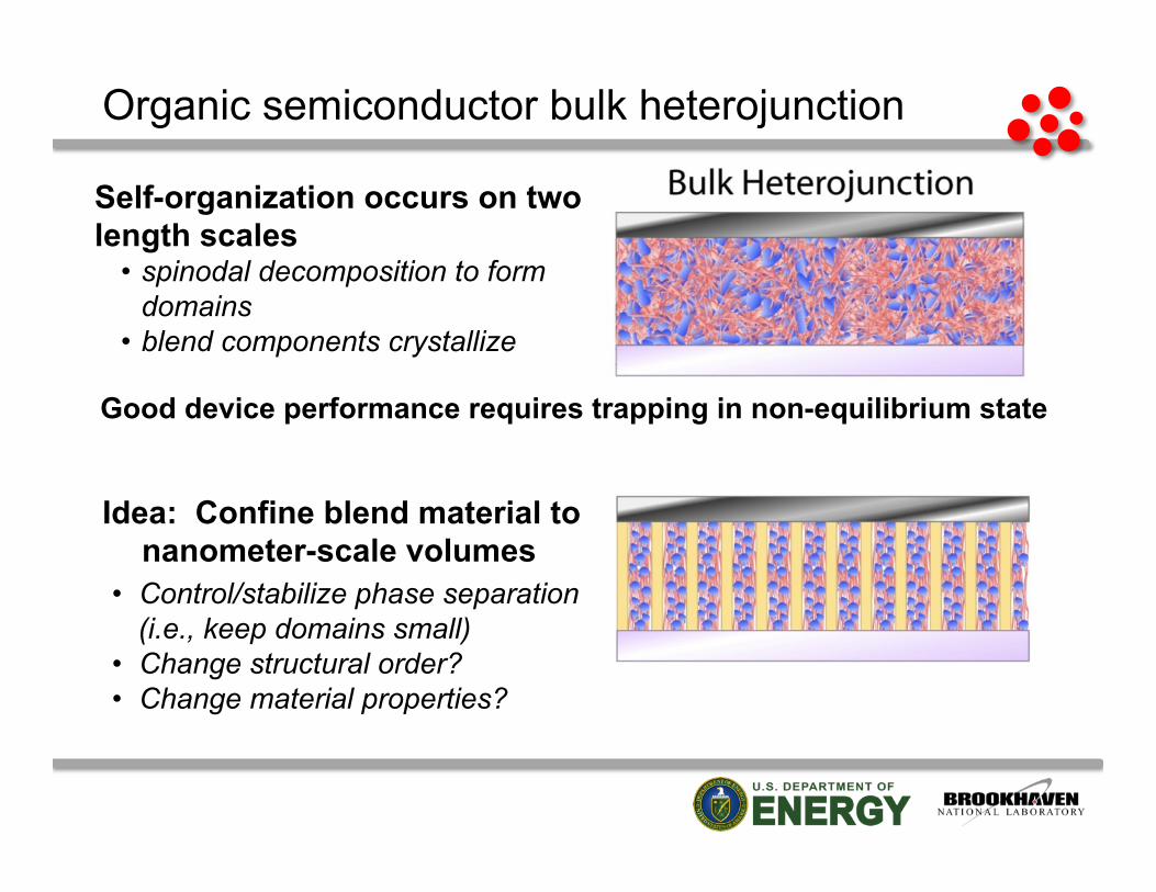
Organic semiconductor bulk heterojunction
Idea: Confine blend material to nanometer-scale volumes
Self-organization occurs on two length scales
• spinodal decomposition to form domains
• blend components crystallize
• Control/stabilize phase separation (i.e., keep domains small)
• Change structural order? • Change material properties?
Good device performance requires trapping in non-equilibrium state

How to pattern an organic material?
Typical lithography: Use organic materials (resists) to pattern inorganics
Our approach: Use inorganic materials to pa9ern organics
apply organic (resist)
pattern organic transfer pattern to inorganic (e.g. metallization)
apply inorganic pattern inorganic
transfer pattern to organic

Controlling P3HT crystal orientation Dan Johnston, CFN
• 40nm linewidth • variable pitch • ~0.5 um line depth • 2x2 mm2 area
500 nm
100 nm
100 nm
Grating re-orients P3HT crystal stacking by 90 degrees
Controlling P3HT crystal orientation Dan Johnston, CFN
P3HT lamellar ~1.7 nm
P3HT π-π (010) ~0.4 nm
PCBM halo ~0.5 nm (300)
(200)
(100)
100 nm
in-plane
out-o
f-pla
ne
(100) (200) (300)
(010)
100 nm
23
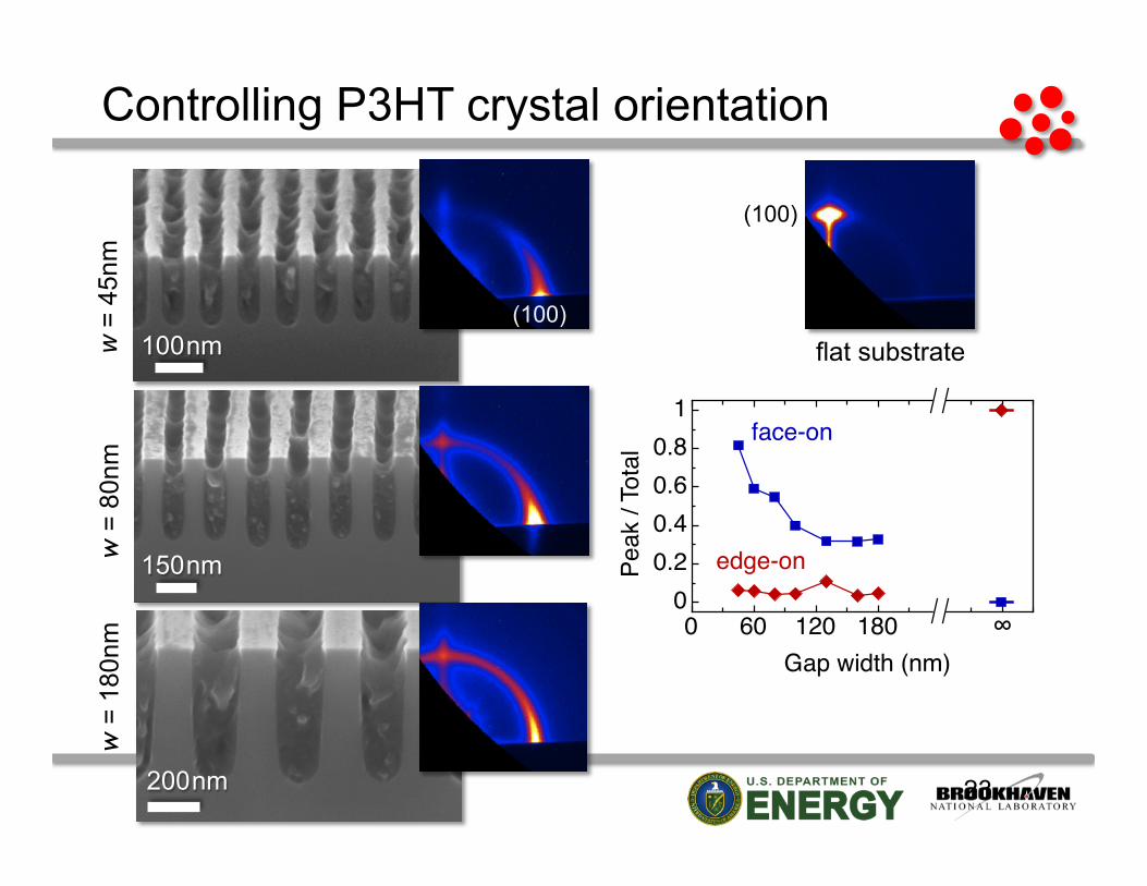
Controlling P3HT crystal orientation
flat substrate
0 60 120 180 240 3000
0.20.40.60.8
1
Gap width (nm)Pe
ak /
Tota
l face-on
edge-on
∞
w =
45n
m
(100)
w =
80n
m
w =
180
nm
(100)
150 nm
200 nm

Self assembly of porous aluminum oxide H. Masuda and K. Fukuda, Science 268 1466 (1995).

Self assembly of porous aluminum oxide
• Tunable nanometer-scale dimensions (size, separation, porosity)
• Extreme aspect ratios possible • Large-area patterning • Reasonable size uniformity • Chemically and thermally robust • Optically transparent • Electrically insulating
20 nm 85 nm 35 nm 65 nm 100 nm 100 nm 100 nm 100 nm
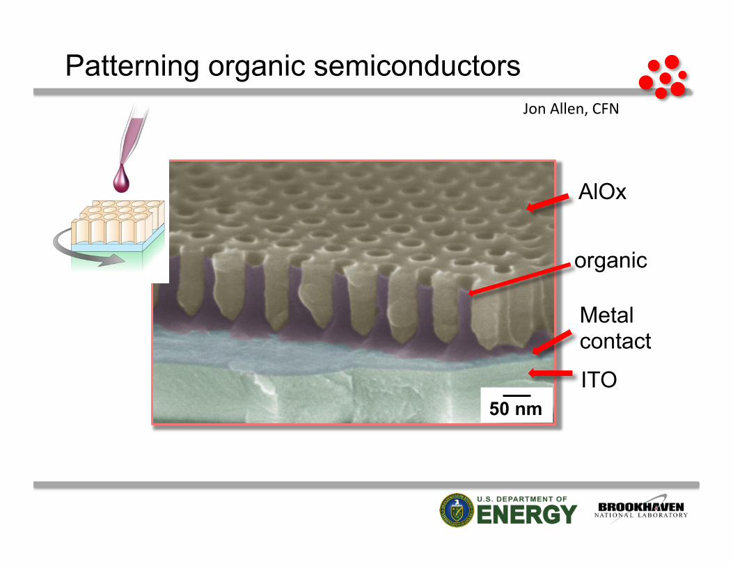
Patterning organic semiconductors
ITO
Metal contact
organic
AlOx
Jon Allen, CFN
50 nm
ITO
V2O5
Aluminum AAO
Organic semiconductor
50 nm
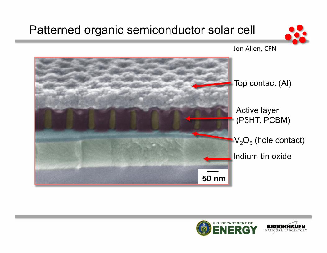
Patterned organic semiconductor solar cell
Indium-tin oxide
V2O5 (hole contact)
Active layer (P3HT: PCBM)
Top contact (Al)
Jon Allen, CFN
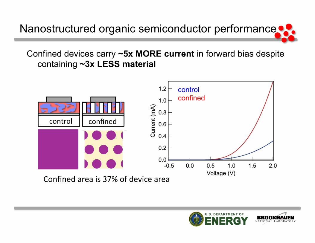
Nanostructured organic semiconductor performance
Confined devices carry ~5x MORE current in forward bias despite containing ~3x LESS material
control confined
Confined area is 37% of device area
confined control
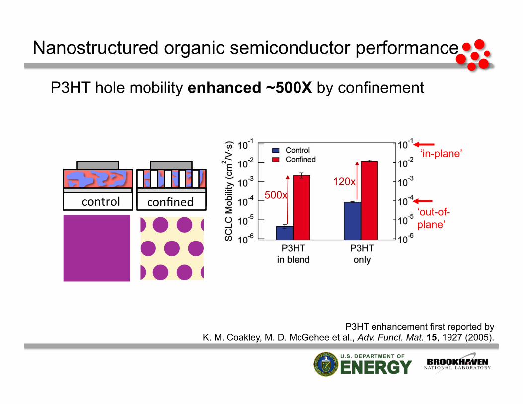
Nanostructured organic semiconductor performance
500x 120x
‘out-of- plane’
‘in-plane’
P3HT hole mobility enhanced ~500X by confinement
P3HT enhancement first reported by K. M. Coakley, M. D. McGehee et al., Adv. Funct. Mat. 15, 1927 (2005).
confined control

confined control
- Reduced scattering intensity (less crystallinity) - Reduced P3HT crystallite size (20nm to 16nm)
• No evidence for 90 degree P3HT reorientation • Rather, confinement disrupts polymer ordering
Confined organic semiconductor structure
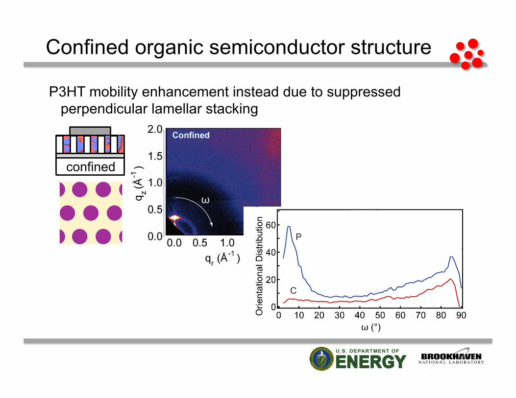
Confined organic semiconductor structure
P3HT mobility enhancement instead due to suppressed perpendicular lamellar stacking
confined
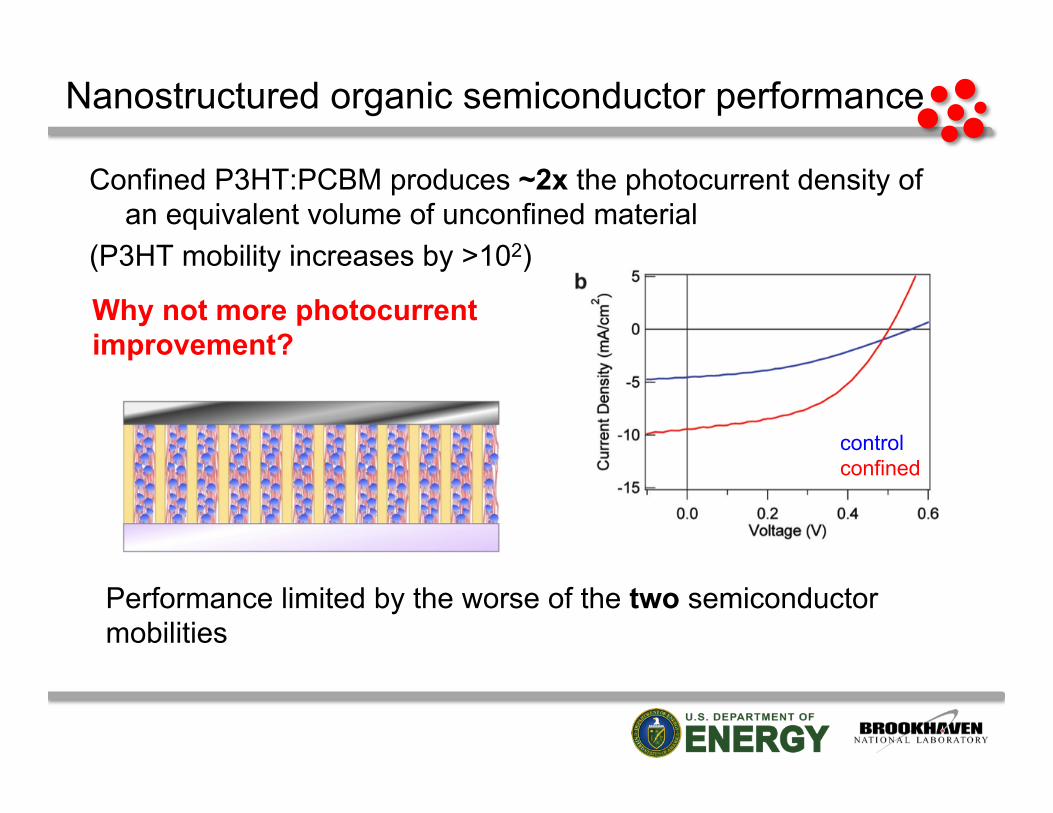
Nanostructured organic semiconductor performance
Confined P3HT:PCBM produces ~2x the photocurrent density of an equivalent volume of unconfined material
(P3HT mobility increases by >102)
control confined
Why not more photocurrent improvement?
Performance limited by the worse of the two semiconductor mobilities

Improving electron collection in confined solar cells
50 nm
Introduce radial contact to shorten electron collection pathway
TiO2 (electron acceptor)
AlOx (template)
planar radial

Improving electron collection in confined solar cells
Confined material performs ~50% better than control Jsc = 15 mA/cm2 (85% of maximum possible)

Leveraging confined polymer advantages
How to best take advantage of performance improvements?
!
" =#2 3
d!$ % & ' ( ) 2* 0.9 d
!$ % & ' ( ) 2
20 nm 85 nm 35 nm 65 nm 100 nm 100 nm 100 nm 100 nm
Maximize template porosity (ϕ) (i.e., minimize wasted space)
90% porosity possible

Leveraging confined polymer advantages
How to best take advantage of performance improvements?
Can we make the entire coaxial structure with polymers?
from Zheng and Wang, Macromolecules (1995).

Message
Self assembly: • Is a tool for device fabrication (similar to lithography) • Provides access to sub-lithographic length scales
Self assembly for semiconductor devices
• Significant challenges to application to technology • Significant advances from groups around the world
Self assembly as a tool for understanding photoconversion
and improving performance • Controlling organic semiconductor structure • Changing organic semiconductor electronic properties
Acknowledgements
IBM group members: Ricardo Ruiz (now at Hitachi) Ying Zhang (now at TSMC) Kathryn Guarini
CFN group members: Jon Allen Dan Johnston
X-rays: Kevin Yager Htay Hlaing (SUNY Stonybrook) Xinhui Liu Ben Ocko
Work supported by Brookhaven Science Associates, LLC under Contract No. DE-AC02-98CH10886 with the U.S. Department of Energy