pn junctions -...
TRANSCRIPT

EE 105 Spring 1997Lecture 5
pn Junctions
■ ubiquitous IC structure -- pn junctions are everywhere!
■ thermal equilibrium: no hole current, no electron current ... no voltage applied between metal interconnects (could short them together)
����
��������
p
nmetal contact ton side
metal contactto p side(Na)
(Nd)
x = 0
(b)
n type
p type����
������
p type
x
x
(a)
EE 105 Spring 1997Lecture 5
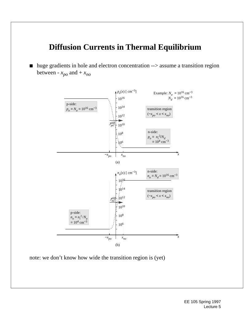
Diffusion Currents in Thermal Equilibrium
■ huge gradients in hole and electron concentration --> assume a transition region between - xpo and + xno
note: we don’t know how wide the transition region is (yet)
106
108p-side:no = ni
2 / Na
= 104 cm−3
n-side:no = Nd = 1016 cm−3
no(x) [ cm−3]
transition region(−xpo < x < xno)
1010
1012
1014
1016
x
Jdiffno
106
108
p-side:po = Na = 1016 cm−3
n-side:po = ni
2 / Nd
= 104 cm−3
po(x) [ cm−3]
transition region(−xpo < x < xno)
Example: Na = 1016 cm−3
Nd = 1016 cm−3
1010
1012
1014
1016
x
Jdiffpo
−xpo xno
−xpo xno
(a)
(b)

EE 105 Spring 1997Lecture 5
Drift and Diffusion in the Transition Region
■ Jno = 0 and Jpo = 0 due to equilibrium
--> negative electric field in the transition region is needed ...
where do + and - charges come from?
■ Answer: the roll-off in electron concentration between x = 0 and xnomeans that
since no(x) < Nd on the n-side of the transition region
■ On the p-side, the charge density is negative, since the hole concentration rolls off between x = - xpo and x = 0.
ρo x( ) q no x( )– Nd+( ) 0>=

EE 105 Spring 1997Lecture 5
Qualitative Electrostatics in Equilibrium
■ From the charge density, we can find the electric field and the potential
φB
φo(x)
φn = 360 mV
φp = −360 mV
−xpo
− qNa = 1.6 × 10⁻³
+ qNd = 1.6 × 10⁻³
xno x
−xpo xno
−xpo xno
Eo(x)
Eo(0)
n-sidep-side
n-sidep-side
n-sidep-side
field foundfrom integralof charge density
x
x
(a)
(b)
(c)
−
+
ρo(x) (C/cm3)

EE 105 Spring 1997Lecture 5
pn Junction in Thermal Equilibrium:Using the Depletion Approximation
■ For detailed calculations, see Section 3.4. Analysis is straightforward, but involved. Use the fact that:
> Charge in depletion region must sum to zero (why?)
> Electrostatic potential is continuous
−xpo
−xpo
xno
xno
x
x
x
ρo(x)
Eo(x)
p-side
(a)
n-side
p-side n-side
−xpo xno
n-side
p-side
+ qNd
− qNa
Eo(x = 0) = −qNdxno
εs
qNaxpo
εs= −
φo(x)
φB
φp
φn
(b)
(c)

Dispositivos Semiconductores
Diode Circuit Symbol and Characteristics
Io: Diode saturation current
EE 105 Spring 1997Lecture 13
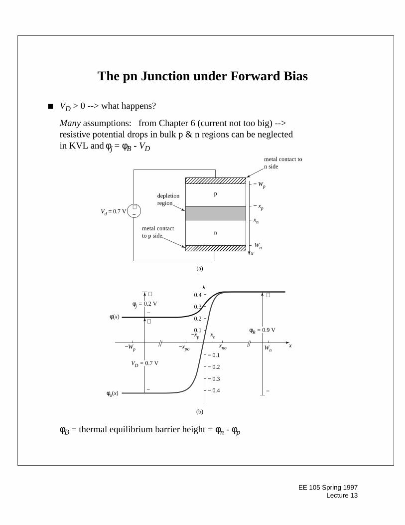
The pn Junction under Forward Bias
■ VD > 0 --> what happens?
Many assumptions: from Chapter 6 (current not too big) -->resistive potential drops in bulk p & n regions can be neglectedin KVL and φj = φB - VD
φB = thermal equilibrium barrier height = φn - φp
��
���
���
��
�������
p
n
xn
− xp
depletion region
metal contact ton side
metal contactto p side
−xpo
−
+
xno
xn−xp0.1
0.2
0.3
0.4
− 0.4
− 0.3
− 0.2
− 0.1
φ(x)
φo(x)
x
(a)
(b)
x
− Wp
Wn
−Wp Wn
Vd = 0.7 V
−+
+
−
VD = 0.7 V
φj = 0.2 V
φB = 0.9 V
+−

EE 105 Spring 1997Lecture 13
Physical Reasoning
■ thermal equilibrium --> balance between drift and diffusion:
J = Jdrift + Jdiff = 0 for holes and electrons
■ forward bias upsets balance
− xpo xnox
(b)
− Wp Wn
− xpo xnox− Wp Wn
−xp xn
(a)
−xpo xnox− Wp Wn
−xp xn
Eo(x)
E(x)
po(x)
p(x)
(c)
−xp xn
Jpo
diff
Jpo
drift
Jp
diff
Jp
drift
Jpo = 0
Jp > 0
Na
linear scale

Dispositivos Semiconductores
P-N junction diode circuit models� Large signal static model

Dispositivos Semiconductores
P-N junction diode circuit models� Small signal model

Dispositivos Semiconductores
P-N junction diode circuit models� Depletion Capacitance
� With reverse bias

Dispositivos Semiconductores