pico embedded high speed cache design...
TRANSCRIPT

PICo Embedded High Speed Cache Design Project TEAM LosTohmalesCalientes
1. INTRODUCTION In this paper we present our design product of a 64Kb high
speed SRAM in the FreePDK 45nm technology. In hopes
to win the contract from the Portable Instruments
Company) PICo, we implemented performance-improving
techniques when designing the main memory body and its
peripherals. The transistor level hierarchical netlist of the
entire SRAM block, block layout, and Cadence simulations
demonstrating proper system functionalities are uploaded to
the team’s Wiki page.
2. DESIGN DESCRIPTION
The Cache SRAM consists of 256*256 ratioed standard 6T
bit cells (8-bit word addressed), an 8 → 256 row decoder, a
5 → 32 word column deMUX, BL/BLB/PRECH logic, 256
high speed sense amplifiers, and a transmission gate
configured column MUX (Figure 1).
Critical design decisions are discussed in the subsections to
follow:
2.1 Multistage Decoders Multistage implementation improves circuit performance
(Rabaey, Chandrakasan, Nikolic, 2002). To reduce reading
& writing access delay, we implemented a NAND/NOR
decoder using 4-input pre-decoders (Figure 2). In the pre-
decode stage, 32 NAND gates output 32 intermediate states
that are re-utilized to compute 256 word line driver inputs.
The sizing of the NAND and NOR gates are calculated
based on a basic logic effort calculation assuming the load
driven is 256xWL_Co* (WL_Co being the estimated single
bit cell load driven by the word line during a read/write
operation).
Similarly, we broke down the word column deMUX into
pre-decode and decode stages.
2.2 BL/BLB/PRECH Logic This logic was responsible for optimizing the bit line, bit
line bar, and precharge circuits, so no extra delay was
incurred as we drove the bit lines for given values. This
was achieved by using one logic block to drive both PMOS
transistors simultaneously on the bit lines.
Chuhong Duan ECE 4332 – Fall 2012 University of Virginia
Andrew Tyler ECE 4332 – Fall 2012 University of Virginia
Rebecca Reed ECE 4332 – Fall 2012 University of Virginia
Lauren Cash ECE 4332 – Fall 2012 University of Virginia
Figure 1. Global Block Diagram
Figure 2. Multistage row decoder implementation
(with 4 → 16 predecode stage)

2.3 High Speed Sense Amplifier Implementing the high-speed sense amp described in Hsu
and Ho’s (2004) conference paper[1], read delays were
nearly cut in half. Essentially, this topology works as a
combination of switches and current sources to more
quickly realize the voltage drop of either bitline or bitline
bar. With this speedup, the read delay became shorter than
the write delay, thus shifting our focus to minimizing write
time.
3. INNOVATION
To further speed up our high-speed SRAM circuit, we
looked into optimizing our peripheral circuits. Specifically,
we knew we could implement a high-speed sense amp.
Implementing the sense amp in Figure 3 we were able to
achieve a 50% speedup from our initial design.
The next place we looked to optimize was the word line
driver. This was a simple innovation – we fed the
BL/BLB/PRECHARGE logic through to both PMOS
transistors on the bit lines. This eliminated the need for an
additional logic unit thus reducing nominal delay.
In order to attain the best performance and minimum metric
consumption (delay power, area), we implemented the
following techniques:
1. Changing/optimizing components topologies
a. Implementing a square (256*256) cache
structure
b. Utilizing combined BL/BLB/PRECH
logic to reduce area and charging delay
c. Breaking row/column decoders into pre-
decode and decode stages
2. Sizing the elements on the critical path
a. Minimizing sizing for elements off
critical path. This reduces total area.
b. Simulating delay vs. driver sizes to find
the optimal sizing for writer drivers
c. Sizing the multistage decoder using basic
logic effort calculations
3. Minimizing layout area by sharing
drain/gate/source inputs and N/P wells
4. Placing row decoder in the middle of SRAM bit
cells
4. SIMULATION AND RESULTS
Due to the size of the SRAM, it was not feasible to
simulate the entire 64 kb cache with all of the periphery
circuits to extract our metrics. Instead, we developed a
stand-in circuit that we could use to calculate active and
inactive metrics; however, this circuit is not a perfect
model. Unfortunately, some of the second-order effects of
the other bit cells and the power consumed by the semi-
active nodes within the decoders are not present in our
simulation. Thankfully, we were able to use our effective
circuit to calculate this power consumption. Additionally,
all process corners were examined in our simulations to
verify the robust functionality of our bit cell under various
conditions.
4.1 Simulation Architecture
To begin, we calculated the effective first-order capacitance
of a bit cell’s output pins and used that value to represent
256 bit cells on the bit and word lines. After determining
the architecture of our decoders and other periphery, we
also used exactly one copy of what would lie attached to
each bit/word line. Our 5:32 word decoder was comprised
of three gates for each output line, so we took one copy of
the three CMOS gates and created an enable bit for our bit
line driving block. We then attached one bit line driving
block to the two bit lines, a capacitance equal to 255 * Ceff
that we calculated through a previous simulation on each
bit line and one sense amp. We also had our sense amp
enable calculation logic, as well as the three gates that
comprised one row decoder connected to the word line.
Also attached to the word line was a capacitance equal to
255 * Ceff, as we calculated previously for the word line
input to a bit cell.
4.2 Simulation Process There were five cases we were most interested in for this
process. To calculate total power consumption, we needed
to simulate a read access, a write access, total inactivity, the
bit lines driven and the word line off, and the word line off
with the bit lines precharged. The total power consumption,
however, is not simply an arithmetic addition of each of
these simulation powers. We instead ran one simulation
with varying input control logic in order to gather data on
the power consumption of each peripheral circuit and the
Figure 3. High Speed Sense Amplifier for Cache
Application (Hsu, Ho, 2004)
bit cell during each transition. Thankfully, Cadence has an
amazing tool under ADE L that allows for the full
exploration of the power of each subcircuit as well as the
current and voltage on each wire. After running each
simulation, we opened the results using this tool to verify
functionality, debug any errors, and collect data on how
different optimizations affected metrics such as delay and
power consumption.
4.3 Simulation Results
Due to the rigidity of our simulation architecture, it was
relatively simple to extract results from each
simulation. For example, using the ADE L Results
Browser, we were able to quickly plot the voltage of the
important signals in our simulation
This tool also has a calculator function that allows for the
computation of average power during different phases and
delay for different simulations without requiring running
the simulation with a new Ocean script.
The simulation graphs we obtained along with the graphs
detailing functionality at the various process corners we
obtained are included at the end of this document. (Figures
8.1-8.5).
5. METRIC COMPUTATION
Calculating the power consumption of our circuit after
optimizing for delay was a relatively simple task given the
simulation setup described previously. We simply
evaluated the average power over a period of 1.5ns, which
was far slower than max speed the circuit was capable of
running, in order to calculate the full energy cost of running
a read or write for each attached component. The final
power consumption also includes the idle power used by
the inactive periphery circuits.
An important metric to note is the sense amp read power.
Our implementation of a faster sense amplifier essentially
doubled our total read power consumption, while halving
our read delay. The extra area was essentially marginal, so
it allowed us to reduce our metric by a factor of roughly
two since delay is squared.
Metric:
Area x x (Access Energy) x (Idle
Power)
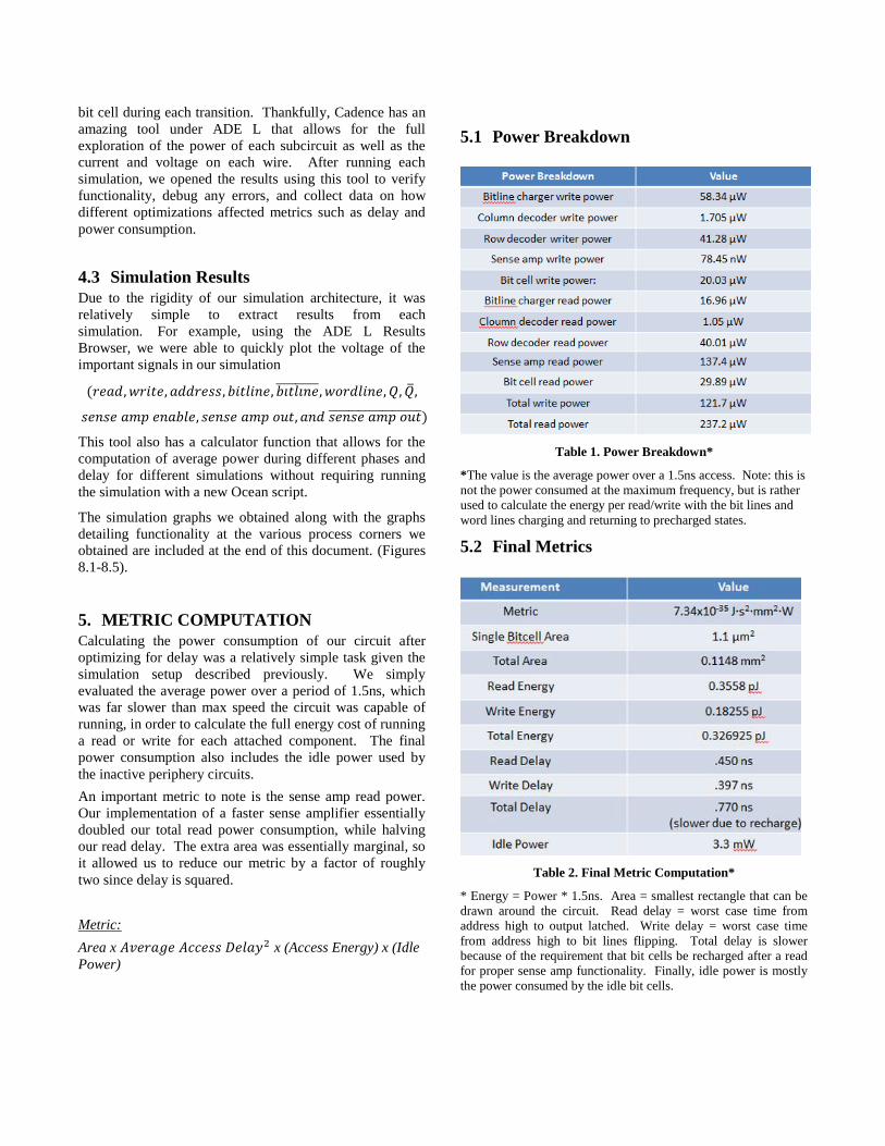
5.1 Power Breakdown
Table 1. Power Breakdown*
*The value is the average power over a 1.5ns access. Note: this is
not the power consumed at the maximum frequency, but is rather
used to calculate the energy per read/write with the bit lines and
word lines charging and returning to precharged states.
5.2 Final Metrics
Table 2. Final Metric Computation*
* Energy = Power * 1.5ns. Area = smallest rectangle that can be
drawn around the circuit. Read delay = worst case time from
address high to output latched. Write delay = worst case time
from address high to bit lines flipping. Total delay is slower
because of the requirement that bit cells be recharged after a read
for proper sense amp functionality. Finally, idle power is mostly
the power consumed by the idle bit cells.

6. CONCLUSION
In this paper, we presented our successful design of a high
speed 64KB SRAM cache. Our metric values are consistent
with our expectations and represent a solid, functional
architecture. We made optimizations to the peripheral
circuits to enhance the speed of the overall SRAM. Our
primary design tool was Cadence and the FreePDK 45nm
technology. The transistor level netlist, block layout, and
Cadence simulations demonstrating proper functionalities
are attached here and on the group Wiki page for review.
As shown by our metrics, we successfully minimized the
critical path delay. We analyzed the tradeoffs between
designs and peripheral circuits and implemented a topology
with the best performance. Overall, our design product
meets all the requirements proposed by PICo, and present
our final design for consideration.
7. REFERENCES
[1] Hsu, C.-L., & Ho, M.-H. (2004). High-speed sense
amplifier for SRAM applications. The 2004 IEEE
Asia-Pacific Conference on Circuits and Systems,
2004. Proceedings (Vol. 1, pp. 577 – 580 vol.1).
Presented at the The 2004 IEEE Asia-Pacific
Conference on Circuits and Systems, 2004.
Proceedings. doi:10.1109/APCCAS.2004.1412828J.
[2] Rabaey, A. Chandrakasan, and B. Nikolic, “Digital
Integrated Circuits – A Design Perspective”, 1995

8. LAYOUT AND SIMULATION GRAPHS
8.1 FULL SCHEMATIC SIMULATION -- TT
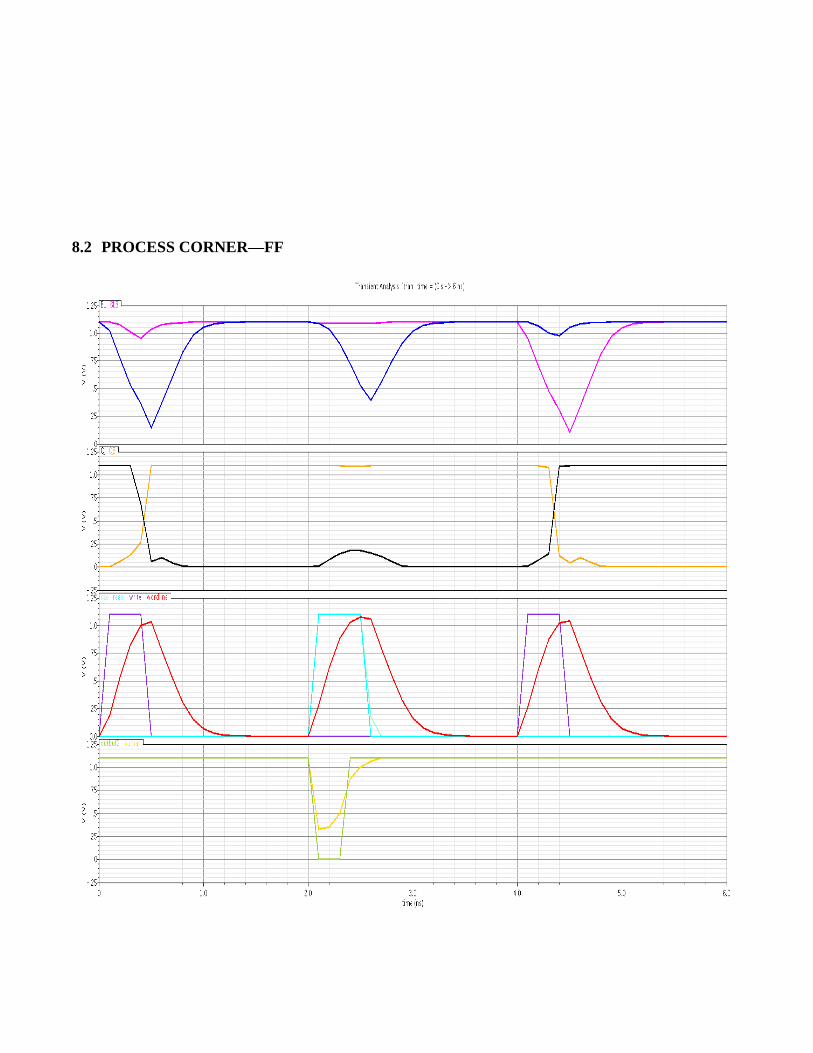
8.2 PROCESS CORNER—FF
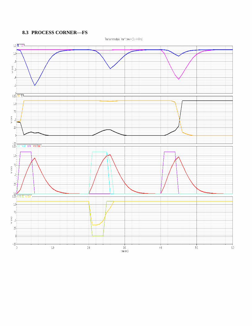
8.3 PROCESS CORNER—FS

8.4 PROCESS CORNER—SF

8.5 PROCESS CORNER – SS

8.6 BIT CELL LAYOUT

8.7 SENSE AMP LAYOUT

8.8 PRECHARGE LAYOUT
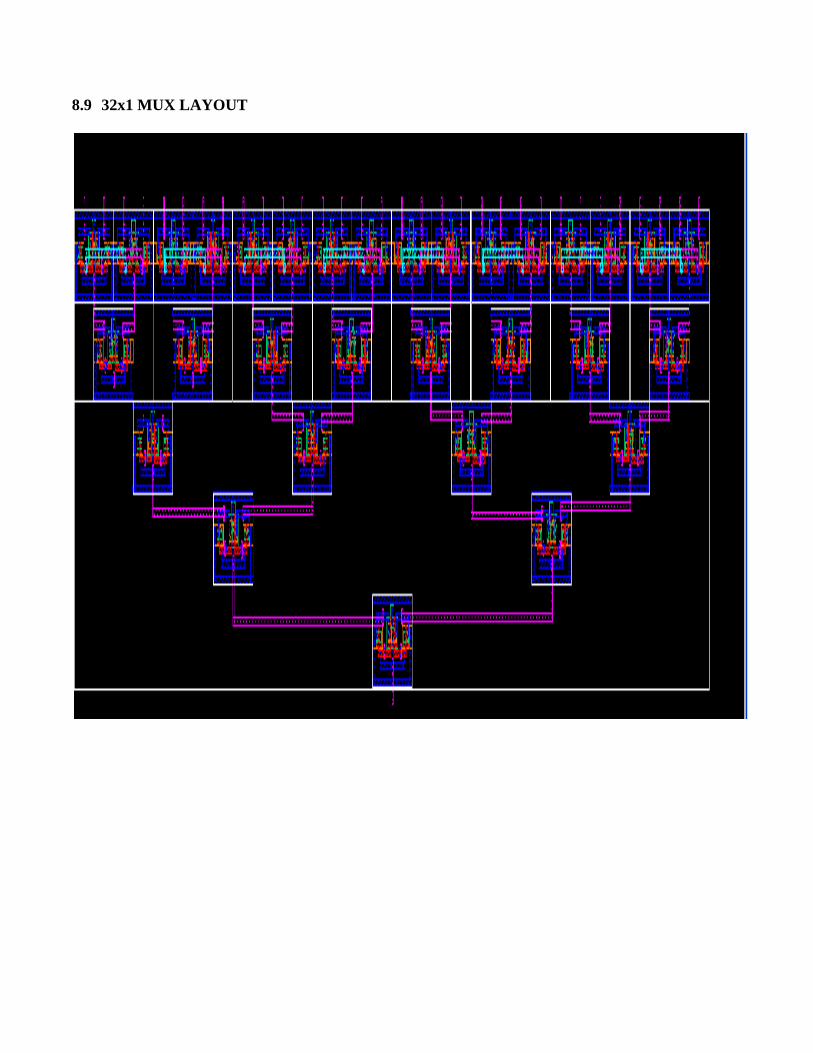
8.9 32x1 MUX LAYOUT

8.10 PREDECODER LAYOUT
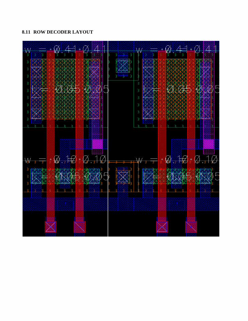
8.11 ROW DECODER LAYOUT

8.12 FULL 64KB LAYOUT