pic16f87/88 data sheet - farnell element14 synchronous serial port (ssp) module ..... 89 11.0...
TRANSCRIPT

2002 Microchip Technology Inc. Advance Information DS30487A
PIC16F87/88Data Sheet
18/20-Pin Enhanced FLASHMicrocontrollers withnanoWatt Technology

Note the following details of the code protection feature on Microchip devices:• Microchip products meet the specification contained in their particular Microchip Data Sheet.
• Microchip believes that its family of products is one of the most secure families of its kind on the market today, when used in the intended manner and under normal conditions.
• There are dishonest and possibly illegal methods used to breach the code protection feature. All of these methods, to our knowl-edge, require using the Microchip products in a manner outside the operating specifications contained in Microchip's Data Sheets. Most likely, the person doing so is engaged in theft of intellectual property.
• Microchip is willing to work with the customer who is concerned about the integrity of their code.
• Neither Microchip nor any other semiconductor manufacturer can guarantee the security of their code. Code protection does not mean that we are guaranteeing the product as “unbreakable.”
Code protection is constantly evolving. We at Microchip are committed to continuously improving the code protection features of ourproducts.
Information contained in this publication regarding deviceapplications and the like is intended through suggestion onlyand may be superseded by updates. It is your responsibility toensure that your application meets with your specifications.No representation or warranty is given and no liability isassumed by Microchip Technology Incorporated with respectto the accuracy or use of such information, or infringement ofpatents or other intellectual property rights arising from suchuse or otherwise. Use of Microchip’s products as critical com-ponents in life support systems is not authorized except withexpress written approval by Microchip. No licenses are con-veyed, implicitly or otherwise, under any intellectual propertyrights.
DS30487A - page ii Advance Info
Trademarks
The Microchip name and logo, the Microchip logo, KEELOQ,MPLAB, PIC, PICmicro, PICSTART and PRO MATE areregistered trademarks of Microchip Technology Incorporatedin the U.S.A. and other countries.
FilterLab, microID, MXDEV, MXLAB, PICMASTER, SEEVALand The Embedded Control Solutions Company areregistered trademarks of Microchip Technology Incorporatedin the U.S.A.
dsPIC, dsPICDEM.net, ECONOMONITOR, FanSense,FlexROM, fuzzyLAB, In-Circuit Serial Programming, ICSP,ICEPIC, microPort, Migratable Memory, MPASM, MPLIB,MPLINK, MPSIM, PICC, PICDEM, PICDEM.net, rfPIC, SelectMode and Total Endurance are trademarks of MicrochipTechnology Incorporated in the U.S.A. and other countries.
Serialized Quick Turn Programming (SQTP) is a service markof Microchip Technology Incorporated in the U.S.A.
All other trademarks mentioned herein are property of theirrespective companies.
© 2002, Microchip Technology Incorporated, Printed in theU.S.A., All Rights Reserved.
Printed on recycled paper.
rmation 2002 Microchip Technology Inc.
Microchip received QS-9000 quality system certification for its worldwide headquarters, design and wafer fabrication facilities in Chandler and Tempe, Arizona in July 1999 and Mountain View, California in March 2002. The Company’s quality system processes and procedures are QS-9000 compliant for its PICmicro® 8-bit MCUs, KEELOQ® code hopping devices, Serial EEPROMs, microperipherals, non-volatile memory and analog products. In addition, Microchip’s quality system for the design and manufacture of development systems is ISO 9001 certified.

PIC16F87/8818/20-Pin Enhanced FLASH MCUs with nanoWatt Technology
Low Power Features: • Power Managed modes:
- Primary RUN XT, RC oscillator, 87 µA,1 MHz, 2V
- RC_RUN 7 µA, 31.25 kHz, 2V- SEC_RUN 14 µA, 32 kHz, 2V- SLEEP 0.2 µA, 2V
• Timer1 oscillator 1.3 µA, 32 kHz, 2V• Watchdog Timer 0.7 µA, 2V• Two-Speed Oscillator Start-up
Oscillators:• Three Crystal modes:
- LP, XT, HS up to 20 MHz• Two External RC modes• One External Clock mode:
- ECIO up to 20 MHz• Internal oscillator block:
- 8 user selectable frequencies: 31 kHz, 125 kHz, 250 kHz, 500 kHz, 1 MHz, 2 MHz, 4 MHz, 8 MHz
Peripheral Features:• Capture, Compare, PWM (CCP) module:
- Capture is 16-bit, max. resolution is 12.5 ns- Compare is 16-bit, max. resolution is 200 ns- PWM max. resolution is 10-bit
• 10-bit, 7-channel Analog-to-Digital Converter• Synchronous Serial Port (SSP) with SPI™
(Master/Slave) and I2C™ (Slave)• Universal Synchronous Asynchronous Receiver
Transmitter (USART/SCI) with 9-bit address detection:- RS-232 operation using internal oscillator
(no external crystal required)• Dual Analog Comparator module:
- Programmable on-chip voltage reference- Programmable input multiplexing from device
inputs and internal voltage reference- Comparator outputs are externally accessible
Pin Diagram
Special Microcontroller Features:• 100,000 erase/write cycles Enhanced FLASH
program memory typical• 1,000,000 typical erase/write cycles EEPROM
data memory typical• EEPROM Data Retention: > 40 years• In-Circuit Serial Programming™ (ICSP™) -
via two pins• Processor read/write access to program memory• Low Voltage Programming• In-Circuit Debugging via two pins• Extended Watchdog Timer (WDT):
- Programmable period from 1 ms to 268s• Wide operating voltage range: 2.0V to 5.5V
RA1/AN1
RA0/AN0
RA7/OSC1/CLKI
RA6/OSC2/CLKO
VDD
RB7/AN6/PGD/
RB6/AN5/PGC/
RB5/SS/TX/CK
RB4/SCK/SCL
RA3/AN3/VREF+/
RA4/AN4/T0CKI/
RA5/MCLR/VPP
VSS
RB0/INT/CCP1(1)
RB1/SDI/SDA
RB2/SDO/RX/DT
RB3/PGM/CCP1(1)
1
2
3
4
5
6
7
8
9
18
17
16
15
14
13
12
11
10
PIC
16F8
8
T1OSI
T1OSO/T1CKI
C2OUT
C1OUT
VREF-RA2/AN2/CVREF/
18-Pin DIP, SOIC
Note 1: The CCP1 pin is determined by CCPMX inConfiguration Word1 register.
DeviceProgram Memory Data Memory
I/O Pins
10-bitA/D (ch)
CCP(PWM) USART Comparators SSP Timers
8/16-bitFLASH(bytes)
# Single Word Instructions
SRAM (bytes)
EEPROM (bytes)
PIC16F87 7168 4096 368 256 16 0 1 Y 2 Y 2/1
PIC16F88 7168 4096 368 256 16 1 1 Y 2 Y 2/1
2002 Microchip Technology Inc. Advance Information DS30487A-page 1

PIC16F87/88
Pin DiagramsRA1/AN1RA0/AN0
RA7/OSC1/CLKIRA6/OSC2/CLKOVDD
RB7/PGD/T1OSI
RB6/PGC/T1OSO/T1CKIRB5/SS/TX/CKRB4/SCK/SCL
RA2/AN2/CVREF
RA3/AN3/C1OUT
RA4/T0CKI/C2OUTRA5/MCLR/VPP
VSS
RB0/INT/CCP1(1)
RB1/SDI/SDARB2/SDO/RX/DT
RB3/PGM/CCP1(1)
1234
5678
9
18171615
14131211
10
PIC
16F8
7
18-Pin DIP, SOIC
RB7/AN6/PGD/T1OSIRB6/AN5/PGC/T1OSO/T1CKI
RA7/OSC1/CLKIRA6/OSC2/CLKOVDD
RB5/SS/TX/CKRB4/SCK/SCLRB3/PGM/CCP1(1)
RB2/SDO/RX/DT
RA0/AN0RA1/AN1
RA4/AN4/T0CKI/C2OUTRA5/MCLR1/VPP
Vss
RA2/AN2/CVREF/VREF-RA3/AN3/VREF+/C1OUT
RB0/INT/CCP1(1)
RB1/SDI/SDA
123456789
201918171615141312
AVDDAVss
10 11
PIC
16F8
8
20-Pin SSOP
20-Pin SSOP
18-Pin DIP & SOIC
RA1/AN1RA0/AN0
RA7/OSC1/CLKIRA6/OSC2/CLKOVDD
RB7/AN6/PGD/T1OSI
RB6/AN5/PGC/T1OSO/T1CKIRB5/SS/TX/CKRB4/SCK/SCL
RA2/AN2/CVREF/VREF-RA3/AN3/VREF+/C1OUT
RA4/AN4/T0CKI/C2OUTRA5/MCLR/VPP
VSS
RB0/INT/CCP1(1)
RB1/SDI/SDARB2/SDO/RX/DT
RB3/PGM/CCP1(1)
1234
5678
9
18171615
14131211
10
PIC
16F8
8
RB7/PGD/T1OSIRB6/PGC/T1OSO/T1CKI
RA7/OSC1/CLKIRA6/OSC2/CLKOVDD
RB5/SS/TX/CKRB4/SCK/SCLRB3/PGM/CCP1(1)
RB2/SDO/RX/DT
RA0/AN0RA1/AN1
RA4/T0CKI/C2OUTRA5/MCLR/VPP
Vss
RA2/AN2/CVREF
RA3/AN3/C1OUT
RB0/INT/CCP1(1)
RB1/SDI/SDA
123456789
201918171615141312
AVDDAVss
10 11
PIC
16F8
7
Note 1: The CCP1 pin is determined by CCPMX in Configuration Word1 register.
DS30487A-page 2 Advance Information 2002 Microchip Technology Inc.

PIC16F87/88
Pin Diagrams (Cont’d)16
2
RA
2/A
N2/
CV
RE
F
RA
0/A
N0
RA
4/T0
CK
I/C2O
UT
RA5/MCLR/VPP
NC
AVssNC
RB0/INT/CCP1(1)R
B1/
SD
I/SD
A
RA
3/AN
3/C
1OU
T
RA7/OSC1/CLKIRA6/OSC2/CLKOVDD
NCAVDD
RB7/PGD/T1OSIRB6/PGC/T1OSO/T1CKI
RB5
/SS
/TX/
CK
RB
4/S
CK/
SC
L
7
PIC16F87
1
3
654
15
21
1920
1718
2228 2627 232425
148 109 131211
VssNC
NC
RA
1/A
N1
RB
2/S
DO
/RX
/DT
RB
3/P
GM
/CC
P1(1
)
NC
NC
NC
16
2
RA
2/A
N2/
CV
RE
F/VR
EF-
RA
0/A
N0
RA
4/A
N4/
T0C
KI/C
2OU
T
RA5/MCLR/VPP
NC
AVSS
NCRB0/INT/CCP1(1)
RB
1/S
DI/S
DA
RA
3/AN
3/V
RE
F+/C
1OU
T
RA7/OSC1/CLKIRA6/OSC2/CLKOVDD
NCAVDD
RB7/PGD/T1OSI/AN6RB6/PGC/T1OSO/T1CKI/AN5
RB5
/SS
/TX/
CK
RB
4/S
CK/
SC
L
7
PIC16F88
1
3
654
15
21
1920
1718
2228 2627 232425
148 109 131211
VSS
NC
NC
RA
1/A
N1
RB
2/S
DO
/RX
/DT
RB
3/P
GM
/CC
P1(1
)
NC
NC
NC
28-Pin QFN
28-Pin QFN
Note 1: The CCP1 pin is determined by CCPMX in Configuration Word1 register.
2002 Microchip Technology Inc. Advance Information DS30487A-page 3

PIC16F87/88
Table of Contents1.0 Device Overview .......................................................................................................................................................................... 52.0 Memory Organization ................................................................................................................................................................. 113.0 Data EEPROM and FLASH Program Memory........................................................................................................................... 274.0 Oscillator Configurations ............................................................................................................................................................ 355.0 I/O Ports ..................................................................................................................................................................................... 536.0 Timer0 Module ........................................................................................................................................................................... 697.0 Timer1 Module ........................................................................................................................................................................... 738.0 Timer2 Module ........................................................................................................................................................................... 819.0 Capture/Compare/PWM (CCP) Module ..................................................................................................................................... 8310.0 Synchronous Serial Port (SSP) Module ..................................................................................................................................... 8911.0 Addressable Universal Synchronous Asynchronous Receiver Transmitter (USART)................................................................ 9912.0 Analog-to-Digital Converter (A/D) Module................................................................................................................................ 11513.0 Comparator Module.................................................................................................................................................................. 12314.0 Comparator Voltage Reference Module................................................................................................................................... 12915.0 Special Features of the CPU.................................................................................................................................................... 13116.0 Instruction Set Summary .......................................................................................................................................................... 15117.0 Development Support............................................................................................................................................................... 15918.0 Electrical Characteristics .......................................................................................................................................................... 16519.0 DC and AC Characteristics Graphs and Tables....................................................................................................................... 19320.0 Packaging Information.............................................................................................................................................................. 195Appendix A: Revision History ............................................................................................................................................................ 201Appendix B: Device Differences......................................................................................................................................................... 201Index .................................................................................................................................................................................................. 203On-Line Support................................................................................................................................................................................. 211Systems Information and Upgrade Hot Line ...................................................................................................................................... 211Reader Response .............................................................................................................................................................................. 212PIC16F87/88 Product Identification System ...................................................................................................................................... 213TO OUR VALUED CUSTOMERSIt is our intention to provide our valued customers with the best documentation possible to ensure successful use of your Microchipproducts. To this end, we will continue to improve our publications to better suit your needs. Our publications will be refined andenhanced as new volumes and updates are introduced. If you have any questions or comments regarding this publication, please contact the Marketing Communications Department viaE-mail at [email protected] or fax the Reader Response Form in the back of this data sheet to (480) 792-4150.We welcome your feedback.
Most Current Data SheetTo obtain the most up-to-date version of this data sheet, please register at our Worldwide Web site at:
http://www.microchip.comYou can determine the version of a data sheet by examining its literature number found on the bottom outside corner of any page.The last character of the literature number is the version number, (e.g., DS30000A is version A of document DS30000).
ErrataAn errata sheet, describing minor operational differences from the data sheet and recommended workarounds, may exist for currentdevices. As device/documentation issues become known to us, we will publish an errata sheet. The errata will specify the revisionof silicon and revision of document to which it applies.To determine if an errata sheet exists for a particular device, please check with one of the following:• Microchip’s Worldwide Web site; http://www.microchip.com• Your local Microchip sales office (see last page)• The Microchip Corporate Literature Center; U.S. FAX: (480) 792-7277When contacting a sales office or the literature center, please specify which device, revision of silicon and data sheet (include liter-ature number) you are using.
Customer Notification SystemRegister on our web site at www.microchip.com/cn to receive the most current information on all of our products.
DS30487A-page 4 Advance Information 2002 Microchip Technology Inc.

PIC16F87/88
1.0 DEVICE OVERVIEWThis document contains device specific information forthe operation of the PIC16F87/88 devices. Additionalinformation may be found in the PICmicro™Mid-Range MCU Reference Manual (DS33023), whichmay be downloaded from the Microchip web site. ThisReference Manual should be considered a comple-mentary document to this data sheet, and is highly rec-ommended reading for a better understanding of thedevice architecture and operation of the peripheralmodules.
The PIC16F87/88 belongs to the Mid-Range family ofthe PICmicro® devices. Block diagrams of the devicesare shown in Figure 1-1 and Figure 1-2. These devicescontain features that are new to the PIC16 product line:
• Low Power modes: The first PIC16 device to have Low Power modes that extend past SLEEP mode. RC_RUN allows the core and peripherals to be clocked from the INTRC, while SEC_RUN allows the core and peripherals to be clocked from the Low Power Timer1. Refer to Section 4.7 for further details.
• Internal RC oscillator with eight selectable frequencies, including 31.25 kHz, 125 kHz, 250 kHz, 500 kHz, 1 MHz, 2 MHz, 4 MHz, and 8 MHz. The INTRC can be configured as a pri-mary or secondary clock source. Refer to Section 4.5 for further details.
• The Timer1 module current consumption has been greatly reduced from 20 µA (previous PIC16 devices) to 1.3 µA typical (32 kHz at 2V), which is ideal for real-time clock applications. Refer to Section 7.0 for further details.
• Extended Watchdog Timer (WDT) that can have a programmable period from 1 ms to 268s. The WDT has its own 16-bit prescaler. Refer to Section 15.12 for further details.
• Two-Speed Start-up: When the oscillator is configured for LP, XT, or HS, this feature will clock the device from the INTRC while the oscillator is warming up. This, in turn, will enable almost immediate code execution. Refer to Section 15.12.4 for further details.
• Fail-Safe Clock Monitor: This feature will allow the device to continue operation if the primary or sec-ondary clock source fails, by switching over to the INTRC.
• The A/D module has a new register for PIC16 devices named ANSEL. This register allow easier configuration of Analog or Digital I/O pins.
TABLE 1-1: AVAILABLE MEMORY IN PIC16F87/88 DEVICES
There are 16 I/O pins that are user configurable on apin-to-pin basis. Some pins are multiplexed with otherdevice functions. These functions include:• External Interrupt• Change on PORTB Interrupt• Timer0 Clock Input• Low Power Timer1 Clock/Oscillator• Capture/Compare/PWM• 10-bit, 7-channel A/D Converter (PIC16F88 only)• SPI/I2C• Two Analog Comparators• USART• MCLR (RA5) can be configured as an Input
Table 1-2 details the pinout of the device withdescriptions and details for each pin.
Device Program FLASH
Data Memory
Data EEPROM
PIC16F87/88 4K x 14 368 x 8 256 x 8
2002 Microchip Technology Inc. Advance Information DS30487A-page 5

PIC16F87/88
FIGURE 1-1: PIC16F87 DEVICE BLOCK DIAGRAMFLASH
ProgramMemory
4K x 14
13 Data Bus 8
14ProgramBus
Instruction reg
Program Counter
8 Level Stack(13-bit)
RAMFile
Registers368 x 8
Direct Addr 7
RAM Addr(1) 9
Addr MUX
IndirectAddr
FSR reg
STATUS reg
MUX
ALU
W reg
Power-upTimer
OscillatorStart-up Timer
Power-onReset
WatchdogTimer
InstructionDecode &
Control
TimingGeneration
OSC1/CLKIOSC2/CLKO
RA5/MCLR VDD, VSS
8
8
Brown-outReset
Note 1: Higher order bits are from the STATUS register.
8
3
Comparators
Timer0
Data EE256 Bytes
Timer1
CCP1
Timer2
USART
PORTA
PORTB
RA4/T0CKI/C2OUT
RB0/INT/CCP1
RA3/AN3/C1OUTRA2/AN2/CVREFRA1/AN1RA0/AN0
RA5/MCLR/VPPRA6/OSC2/CLKO
RB5/SS/TX/CKRB4/SCK/SCLRB3/PGM/CCP1RB2/SDO/RX/DTRB1/SDI/SDA
RB6/PGC/T1OSO/T1CKIRB7/PGD/T1OSI
RA7/OSC1/CLKI
AVDD, AVSS
SSP
DS30487A-page 6 Advance Information 2002 Microchip Technology Inc.

PIC16F87/88
FIGURE 1-2: PIC16F88 DEVICE BLOCK DIAGRAMFLASH
ProgramMemory
4K x 14
13 Data Bus 8
14ProgramBus
Instruction reg
Program Counter
8 Level Stack(13-bit)
RAMFile
Registers368 x 8
Direct Addr 7
RAM Addr(1) 9
Addr MUX
IndirectAddr
FSR reg
STATUS reg
MUX
ALU
W reg
Power-upTimer
OscillatorStart-up Timer
Power-onReset
WatchdogTimer
InstructionDecode &
Control
TimingGeneration
OSC1/CLKIOSC2/CLKO
RA5/MCLR VDD, VSS
8
8
Brown-outReset
Note 1: Higher order bits are from the STATUS register.
8
3
Comparators
Timer0
Data EE256 Bytes
Timer1
CCP1
Timer2
USART
PORTA
PORTB
RA4/AN4/T0CKI/C2OUT
RB0/INT/CCP1
RA3/AN3/VREF+/C1OUTRA2/AN2/CVREF/VREF-RA1/AN1RA0/AN0
RA5/MCLR/VPPRA6/OSC2/CLKO
RB5/SS/TX/CKRB4/SCK/SCLRB3/PGM/CCP1RB2/SDO/RX/DTRB1/SDI/SDA
RB6/AN5/PGC/T1OSO/T1CKIRB7/AN6/PGD/T1OSI
RA7/OSC1/CLKI
10-bit A/D
AVDD, AVSS
SSP
2002 Microchip Technology Inc. Advance Information DS30487A-page 7

PIC16F87/88
TABLE 1-2: PIC16F87/88 PINOUT DESCRIPTIONPin NamePDIP/SOICPin#
SSOPPin#
QFNPin#
I/O/PType
BufferType Description
PORTA is a bi-directional I/O port.
RA0/AN0RA0AN0
17 19 23I/OI
TTLAnalog
Bi-directional I/O pin.Analog input channel 0.
RA1/AN1RA1AN1
18 20 24I/OI
TTLAnalog
Bi-directional I/O pin.Analog input channel 1.
RA2/CVREF/AN2/VREF-RA2CVREFAN2VREF-(4)
1 1 26I/OOII
TTL
AnalogAnalog
Bi-directional I/O pin.Comparator VREF output.Analog input channel 2.A/D reference voltage (Low) input.
RA3/AN3/VREF+/C1OUTRA3AN3VREF+(4)
C1OUT
2 2 27I/OIIO
TTLAnalogAnalog
Bi-directional I/O pin.Analog input channel 3.A/D reference voltage (High) input.Comparator1 output.
RA4/AN4/T0CKI/C2OUTRA4AN4(4)
T0CKIC2OUT
3 3 28I/OIIO
STAnalog
ST
Bi-directional I/O pin.Analog input channel 4.Clock input to the TMR0 timer/counter.Comparator2 output.
RA5/MCLR/VPPRA5MCLR
VPP
4 4 1II
P
STST
–
Input pin. Master Clear (Reset). Input/programming voltage input. This pin is an active low RESET to the device. Programming voltage input.
RA6/OSC2/CLKORA6OSC2
CLKO
15 17 20I/OO
O
ST–
–
Bi-directional I/O pin. Oscillator crystal output. Connects to crystal or resonator in Crystal Oscillator mode. In RC mode, this pin outputs CLKO signal, which has 1/4 the frequency of OSC1, and denotes the instruction cycle rate.
RA7/OSC1/CLKIRA7OSC1CLKI
16 18 21I/OII
STST/CMOS(3)
–
Bi-directional I/O pin.Oscillator crystal input.External clock source input.
Legend: I = Input O = Output I/O = Input/Output P = Power– = Not used TTL = TTL Input ST = Schmitt Trigger Input
Note 1: This buffer is a Schmitt Trigger input when configured as the external interrupt.2: This buffer is a Schmitt Trigger input when used in Serial Programming mode.3: This buffer is a Schmitt Trigger input when configured in RC Oscillator mode and a CMOS input otherwise.4: PIC16F88 devices only.
DS30487A-page 8 Advance Information 2002 Microchip Technology Inc.

PIC16F87/88
PORTB is a bi-directional I/O port. PORTB can be software programmed for internal weak pull-up on all inputs.
RB0/INT/CCP1RB0INTCCP1
6 7 7I/OI
I/O
TTLST(1)
ST
Bi-directional I/O pin.External interrupt pin.Capture input, Compare output, PWM output.
RB1/SDI/SDARB1SDISDA
7 8 8I/OI
I/O
TTLSTST
Bi-directional I/O pin.SPI Data in.I2C Data.
RB2/SDO/RX/DTRB2SDORXDT
8 9 9I/OOI
I/O
TTLST
Bi-directional I/O pin.SPI Data out.USART asynchronous receive.USART synchronous detect.
RB3/CCP1/PGMRB3CCP1PGM
9 10 10I/OI/OI
TTLSTST
Bi-directional I/O pin.Capture input, Compare output, PWM output.Low Voltage ICSP programming enable pin.
RB4/SCK/SCLRB4SCKSCL
10 11 12I/OI/OI
TTLSTST
Bi-directional I/O pin. Interrupt-on-change pin.Synchronous serial clock input/output for SPI.Synchronous serial clock Input for I2C.
RB5/SS/TX/CKRB5SSTXCK
11 12 13I/OIOI/O
TTLTTL
Bi-directional I/O pin. Interrupt-on-change pin.Slave select for SPI in Slave mode.USART asynchronous transmit.USART synchronous clock.
RB6/T1OSO/T1CKI/PGC/AN5
RB6T1OSOT1CKIPGCAN5(4)
12 13 15
I/OOI
I/OI
TTLSTST
ST(2)
Bi-directional I/O pin. Interrupt-on-change pin.Timer1 Oscillator output.Timer1 external clock input.In-circuit debugger and programming clock pin.Analog input channel 5.
RB7/T1OSI/PGD/AN6RB7T1OSIPGDAN6(4)
13 14 16I/OIII
TTLST
ST(2)
Bi-directional I/O pin. Interrupt-on-change pin. Timer1 Oscillator input.In-circuit debugger and ICSP programming data pin.Analog input channel 6.
VSS 5 5, 6 3, 5 P – Ground reference for logic and I/O pins.
VDD 14 15, 16 17, 19 P – Positive supply for logic and I/O pins.
TABLE 1-2: PIC16F87/88 PINOUT DESCRIPTION (CONTINUED)
Pin NamePDIP/SOICPin#
SSOPPin#
QFNPin#
I/O/PType
BufferType Description
Legend: I = Input O = Output I/O = Input/Output P = Power– = Not used TTL = TTL Input ST = Schmitt Trigger Input
Note 1: This buffer is a Schmitt Trigger input when configured as the external interrupt.2: This buffer is a Schmitt Trigger input when used in Serial Programming mode.3: This buffer is a Schmitt Trigger input when configured in RC Oscillator mode and a CMOS input otherwise.4: PIC16F88 devices only.
2002 Microchip Technology Inc. Advance Information DS30487A-page 9

PIC16F87/88
NOTES:DS30487A-page 10 Advance Information 2002 Microchip Technology Inc.

PIC16F87/88
2.0 MEMORY ORGANIZATIONThere are two memory blocks in the PIC16F87/88.These are the program memory and the data memory.Each block has its own bus, so access to each blockcan occur during the same oscillator cycle.The data memory can be further broken down into thegeneral purpose RAM and the Special FunctionRegisters (SFRs). The operation of the SFRs thatcontrol the “core” are described here. The SFRs usedto control the peripheral modules are described in thesection discussing each individual peripheral module.
The data memory area also contains the dataEEPROM memory. This memory is not directlymapped into the data memory, but is indirectlymapped. That is, an indirect address pointer specifiesthe address of the data EEPROM memory to read/write. The PIC16F87/88’s 256 bytes of data EEPROMmemory have the address range 00h-FFh. More detailson the EEPROM memory can be found in Section 3.0.
Additional information on device memory may be foundin the PICmicro™ Mid-Range Reference Manual,(DS33023).
2.1 Program Memory OrganizationThe PIC16F87/88 devices have a 13-bit programcounter capable of addressing an 8K x 14 programmemory space. For the PIC16F87/88, the first 4K x 14(0000h-0FFFh) is physically implemented (seeFigure 2-1). Accessing a location above the physicallyimplemented address will cause a wraparound. Forexample, the same instruction will be accessed at loca-tions 020h, 420h, 820h, C20h, 1020h, 1420h, 1820h,and 1C20h.
The RESET vector is at 0000h and the interrupt vectoris at 0004h.
FIGURE 2-1: PROGRAM MEMORY MAP AND STACK FOR PIC16F87/88
2.2 Data Memory OrganizationThe Data Memory is partitioned into multiple banks thatcontain the General Purpose Registers and the SpecialFunction Registers. Bits RP1 (STATUS<6>) and RP0(STATUS<5>) are the bank select bits.
Each bank extends up to 7Fh (128 bytes). The lowerlocations of each bank are reserved for the SpecialFunction Registers. Above the Special Function Regis-ters are General Purpose Registers, implemented asstatic RAM. All implemented banks contain SFRs.Some “high use” SFRs from one bank may be mirroredin another bank for code reduction and quicker access(e.g., the STATUS register is in Banks 0 - 3).
RP1:RP0 Bank
00 001 110 211 3
Note: EEPROM Data Memory description can befound in Section 3.0 of this data sheet.
PC<12:0>
13
0000h
0004h0005h
Stack Level 1
Stack Level 8
RESET Vector
Interrupt VectorOn-chip
CALL, RETURNRETFIE, RETLW
1FFFh
Stack Level 2
ProgramMemory
Page 007FFh
Wraps to0000h - 03FFh
Page 10FFFh1000h
0800h
2002 Microchip Technology Inc. Advance Information DS30487A-page 11

PIC16F87/88
2.2.1 GENERAL PURPOSE REGISTER FILEThe register file can be accessed either directly, orindirectly through the File Select Register FSR.
FIGURE 2-2: PIC16F87 REGISTER FILE MAP
Indirect addr.(*)
TMR0PCL
STATUSFSR
PORTAPORTB
PCLATHINTCON
PIR1
OPTIONPCL
STATUSFSR
TRISATRISB
PCLATHINTCON
PIE1
PCON
00h01h02h03h04h05h06h07h08h09h0Ah0Bh0Ch0Dh0Eh0Fh10h11h12h13h14h15h16h17h18h19h1Ah1Bh1Ch1Dh1Eh1Fh
80h81h82h83h84h85h86h87h88h89h8Ah8Bh8Ch8Dh8Eh8Fh90h91h92h93h94h95h96h97h98h99h9Ah9Bh9Ch9Dh9Eh9Fh
20h A0h
7Fh FFhBank 0 Bank 1
Unimplemented data memory locations, read as ‘0’. * Not a physical register.
Note 1: This register is reserved, maintain this register clear.
FileAddress
Indirect addr.(*) Indirect addr.(*)
PCLSTATUS
FSR
PCLATHINTCON
PCLSTATUS
FSR
PCLATHINTCON
100h101h102h103h104h105h106h107h108h109h10Ah10Bh
180h181h182h183h184h185h186h187h188h189h18Ah18Bh
Indirect addr.(*)
CVRCON
TMR0 OPTION
PIR2 PIE2
GeneralPurposeRegister
accesses70h-7Fh
TRISBPORTB
96 BytesEFhF0h
10Ch10Dh10Eh10Fh110h
18Ch18Dh18Eh18Fh190h
EEDATAEEADR
EECON1EECON2
EEDATHEEADRH
Reserved(1)
Reserved(1)
17Fh 1FFhBank 2 Bank 3
19Fh1A0h
accesses70h - 7Fh
11Fh120h
accesses70h-7Fh
CMCON
OSCCON
GeneralPurposeRegister80 Bytes
TMR1LTMR1HT1CONTMR2T2CON
CCPR1LCCPR1H
CCP1CONRCSTATXREGRCREG
PR2
TXSTASPBRG
OSCTUNE
WDTCON
16Fh170h
GeneralPurposeRegister80 Bytes
1EFh1F0h
GeneralPurposeRegister80 Bytes
GeneralPurposeRegister16 Bytes
GeneralPurposeRegister16 Bytes
SSPBUFSSPCON1
SSPADDSSPSTAT
FileAddress
FileAddress
FileAddress
DS30487A-page 12 Advance Information 2002 Microchip Technology Inc.

PIC16F87/88
FIGURE 2-3: PIC16F88 REGISTER FILE MAPIndirect addr.(*)
TMR0PCL
STATUSFSR
PORTAPORTB
PCLATHINTCON
PIR1
OPTIONPCL
STATUSFSR
TRISATRISB
PCLATHINTCON
PIE1
PCON
00h01h02h03h04h05h06h07h08h09h0Ah0Bh0Ch0Dh0Eh0Fh10h11h12h13h14h15h16h17h18h19h1Ah1Bh1Ch1Dh1Eh1Fh
80h81h82h83h84h85h86h87h88h89h8Ah8Bh8Ch8Dh8Eh8Fh90h91h92h93h94h95h96h97h98h99h9Ah9Bh9Ch9Dh9Eh9Fh
20h A0h
7Fh FFhBank 0 Bank 1
Unimplemented data memory locations, read as ‘0’. * Not a physical register.
Note 1: This register is reserved, maintain this register clear.
FileAddress
Indirect addr.(*) Indirect addr.(*)
PCLSTATUS
FSR
PCLATHINTCON
PCLSTATUS
FSR
PCLATHINTCON
100h101h102h103h104h105h106h107h108h109h10Ah10Bh
180h181h182h183h184h185h186h187h188h189h18Ah18Bh
Indirect addr.(*)
TMR0 OPTION
PIR2 PIE2
ADRESHADCON0 ADCON1
GeneralPurposeRegister
accesses70h-7Fh
TRISBPORTB
96 Bytes
10Ch10Dh10Eh10Fh110h
18Ch18Dh18Eh18Fh190h
EEDATAEEADR
EECON1EECON2
EEDATHEEADRH
Reserved(1)
Reserved(1)
17Fh 1FFhBank 2 Bank 3
19Fh1A0h
11Fh120h
CVRCON
OSCCON
CMCON
ADRESL
TMR1LTMR1HT1CONTMR2
CCPR1LCCPR1H
CCP1CONRCSTATXREGRCREG
PR2
TXSTASPBRG
T2CON
OSCTUNE
WDTCON
EFhF0h
GeneralPurposeRegister80 Bytes
16Fh170h
GeneralPurposeRegister80 Bytes
1EFh1F0h
GeneralPurposeRegister80 Bytes
GeneralPurposeRegister16 Bytes
GeneralPurposeRegister16 Bytes
accesses70h - 7Fh
accesses70h-7Fh
SSPBUFSSPCON1
SSPADDSSPSTAT
ANSEL
FileAddress
FileAddress
FileAddress
2002 Microchip Technology Inc. Advance Information DS30487A-page 13

PIC16F87/88
2.2.2 SPECIAL FUNCTION REGISTERSThe Special Function Registers are registers used bythe CPU and peripheral modules for controlling thedesired operation of the device. These registers areimplemented as static RAM. A list of these registers isgiven in Table 2-1.
The Special Function Registers can be classified intotwo sets: core (CPU) and peripheral. Those registersassociated with the core functions are described indetail in this section. Those related to the operation ofthe peripheral features are described in detail in theperipheral feature section.
TABLE 2-1: SPECIAL FUNCTION REGISTER SUMMARY
Address Name Bit 7 Bit 6 Bit 5 Bit 4 Bit 3 Bit 2 Bit 1 Bit 0 Value on:POR, BOR
Bank 000h(2) INDF Addressing this location uses contents of FSR to address data memory
(not a physical register)0000 0000
01h TMR0 Timer0 Module Register xxxx xxxx02h(2) PCL Program Counter (PC) Least Significant Byte 0000 000003h(2) STATUS IRP RP1 RP0 TO PD Z DC C 0001 1xxx04h(2) FSR Indirect Data Memory Address Pointer xxxx xxxx05h PORTA - 87
PORTA - 88PORTA Data Latch when written; PORTA pins when read xxxx 0000
xxx0 000006h PORTB - 87
PORTB - 88PORTB Data Latch when written; PORTB pins when read xxxx xxxx
00xx xxxx07h — Unimplemented —08h — Unimplemented —09h — Unimplemented —0Ah(1,2) PCLATH — — — Write Buffer for the upper 5 bits of the Program Counter ---0 00000Bh(2) INTCON GIE PEIE TMR0IE INT0IE RBIE TMR0IF INT0IF RBIF 0000 000x0Ch PIR1 — ADIF RCIF TXIF SSPIF CCP1IF TMR2IF TMR1IF -000 00000Dh PIR2 OSFIF CMIF — EEIF — — — — 00-0 ----0Eh TMR1L Holding Register for the Least Significant Byte of the 16-bit TMR1 Register xxxx xxxx0Fh TMR1H Holding Register for the Most Significant Byte of the 16-bit TMR1 Register xxxx xxxx10h T1CON — T1RUN T1CKPS1 T1CKPS0 T1OSCEN T1SYNC TMR1CS TMR1ON -000 000011h TMR2 Timer2 Module Register 0000 000012h T2CON — TOUTPS3 TOUTPS2 TOUTPS1 TOUTPS0 TMR2ON T2CKPS1 T2CKPS0 -000 000013h SSPBUF Synchronous Serial Port Receive Buffer/Transmit Register xxxx xxxx14h SSPCON WCOL SSPOV SSPEN CKP SSPM3 SSPM2 SSPM1 SSPM0 0000 000015h CCPR1L Capture/Compare/PWM Register1 (LSB) xxxx xxxx16h CCPR1H Capture/Compare/PWM Register1 (MSB) xxxx xxxx17h CCP1CON — — CCP1X CCP1Y CCP1M3 CCP1M2 CCP1M1 CCP1M0 --00 000018h RCSTA SPEN RX9 SREN CREN ADDEN FERR OERR RX9D 0000 000x19h TXREG USART Transmit Data Register 0000 00001Ah RCREG USART Receive Data Register 0000 00001Bh — Unimplemented —1Ch — Unimplemented —1Dh — Unimplemented —1Eh ADRESH(4) A/D Result Register High Byte xxxx xxxx1Fh ADCON0(4) ADCS1 ADCS0 CHS2 CHS1 CHS0 GO/DONE — ADON 0000 00-0Legend: x = unknown, u = unchanged, q = value depends on condition, - = unimplemented, read as '0', r = reserved.
Shaded locations are unimplemented, read as ‘0’.Note 1: The upper byte of the program counter is not directly accessible. PCLATH is a holding register for the PC<12:8>, whose
contents are transferred to the upper byte of the program counter.2: These registers can be addressed from any bank.3: Pin 5 is an input only; the state of the TRISA5 bit has no effect and will always read ‘1’.4: PIC16F88 device only.
DS30487A-page 14 Advance Information 2002 Microchip Technology Inc.

PIC16F87/88
Bank 180h(2) INDF Addressing this location uses contents of FSR to address data memory
(not a physical register)0000 0000
81h OPTION RBPU INTEDG T0CS T0SE PSA PS2 PS1 PS0 1111 111182h(2) PCL Program Counter (PC) Least Significant Byte 0000 000083h(2) STATUS IRP RP1 RP0 TO PD Z DC C 0001 1xxx84h(2) FSR Indirect Data Memory Address Pointer xxxx xxxx85h TRISA TRISA7 TRISA6 TRISA5(3) PORTA Data Direction Register (TRISA<4:0>) 1111 111186h TRISB PORTB Data Direction Register 1111 111187h — Unimplemented —88h — Unimplemented —89h — Unimplemented —8Ah(1,2) PCLATH — — — Write Buffer for the upper 5 bits of the Program Counter ---0 00008Bh(2) INTCON GIE PEIE TMR0IE INT0IE RBIE TMR0IF INT0IF RBIF 0000 000x8Ch PIE1 — ADIE RCIE TXIE SSPIE CCP1IE TMR2IE TMR1IE -000 00008Dh PIE2 OSFIE CMIE — EEIE — — — — 00-0 ----8Eh PCON — — — — — — POR BOR ---- --qq8Fh OSCCON — IRCF2 IRCF1 IRCF0 OSTS IOFS SCS1 SCS0 -000 000090h OSCTUNE — — TUN5 TUN4 TUN3 TUN2 TUN1 TUN0 --00 000091h — Unimplemented —92h PR2 Timer2 Period Register 1111 111193h SSPADD Synchronous Serial Port (I2C mode) Address Register 0000 000094h SSPSTAT SMP CKE D/A P S R/W UA BF 0000 000095h — Unimplemented —96h — Unimplemented —97h — Unimplemented —98h TXSTA CSRC TX9 TXEN SYNC — BRGH TRMT TX9D 0000 -01099h SPBRG Baud Rate Generator Register 0000 00009Ah — Unimplemented —9Bh ANSEL(4) — ANS6 ANS5 ANS4 ANS3 ANS2 ANS1 ANS0 -111 11119Ch CMCON C2OUT C1OUT C2INV C1INV CIS CM2 CM1 CM0 0000 00009Dh CVRCON CVREN CVROE CVRR — CVR3 CVR2 CVR1 CVR0 000- 00009Eh ADRESL(4) A/D Result Register Low Byte xxxx xxxx9Fh ADCON1(4) ADFM ADCS2 VCFG1 VCFG0 — — — — 0000 ----
TABLE 2-1: SPECIAL FUNCTION REGISTER SUMMARY (CONTINUED)
Address Name Bit 7 Bit 6 Bit 5 Bit 4 Bit 3 Bit 2 Bit 1 Bit 0 Value on:POR, BOR
Legend: x = unknown, u = unchanged, q = value depends on condition, - = unimplemented, read as '0', r = reserved. Shaded locations are unimplemented, read as ‘0’.
Note 1: The upper byte of the program counter is not directly accessible. PCLATH is a holding register for the PC<12:8>, whose contents are transferred to the upper byte of the program counter.
2: These registers can be addressed from any bank.3: Pin 5 is an input only; the state of the TRISA5 bit has no effect and will always read ‘1’.4: PIC16F88 device only.
2002 Microchip Technology Inc. Advance Information DS30487A-page 15

PIC16F87/88
Bank 2100h(2) INDF Addressing this location uses contents of FSR to address data memory
(not a physical register)0000 0000
101h TMR0 Timer0 Module Register xxxx xxxx102h(2) PCL Program Counter's (PC) Least Significant Byte 0000 0000103h(2) STATUS IRP RP1 RP0 TO PD Z DC C 0001 1xxx104h(2) FSR Indirect Data Memory Address Pointer xxxx xxxx105h WDTCON — — — WDTPS3 WDTPS2 WDTPS1 WDTPS0 SWDTEN ---0 1000106h PORTB PORTB Data Latch when written; PORTB pins when read xxxx xxxx107h — Unimplemented —108h — Unimplemented —109h — Unimplemented —10Ah(1,2) PCLATH — — — Write Buffer for the upper 5 bits of the Program Counter ---0 000010Bh(2) INTCON GIE PEIE TMR0IE INT0IE RBIE TMR0IF INT0IF RBIF 0000 000x10Ch EEDATA EEPROM Data Register Low Byte xxxx xxxx10Dh EEADR EEPROM Address Register Low Byte xxxx xxxx10Eh EEDATH — — EEPROM Data Register High Byte --xx xxxx10Fh EEADRH — — — — EEPROM Address Register High Byte ---- xxxx Bank 3180h(2) INDF Addressing this location uses contents of FSR to address data memory
(not a physical register)0000 0000
181h OPTION RBPU INTEDG T0CS T0SE PSA PS2 PS1 PS0 1111 1111182h(2) PCL Program Counter (PC) Least Significant Byte 0000 0000183h(2) STATUS IRP RP1 RP0 TO PD Z DC C 0001 1xxx184h(2) FSR Indirect Data Memory Address Pointer xxxx xxxx185h — Unimplemented —186h TRISB PORTB Data Direction Register 1111 1111187h — Unimplemented —188h — Unimplemented —189h — Unimplemented —18Ah(1,2) PCLATH — — — Write Buffer for the upper 5 bits of the Program Counter ---0 000018Bh(2) INTCON GIE PEIE TMR0IE INT0IE RBIE TMR0IF INT0IF RBIF 0000 000x18Ch EECON1 EEPGD — — FREE WRERR WREN WR RD x--x x00018Dh EECON2 EEPROM Control Register2 (not a physical register) ---- ----18Eh — Reserved, maintain clear 0000 000018Fh — Reserved, maintain clear 0000 0000
TABLE 2-1: SPECIAL FUNCTION REGISTER SUMMARY (CONTINUED)
Address Name Bit 7 Bit 6 Bit 5 Bit 4 Bit 3 Bit 2 Bit 1 Bit 0 Value on:POR, BOR
Legend: x = unknown, u = unchanged, q = value depends on condition, - = unimplemented, read as '0', r = reserved. Shaded locations are unimplemented, read as ‘0’.
Note 1: The upper byte of the program counter is not directly accessible. PCLATH is a holding register for the PC<12:8>, whose contents are transferred to the upper byte of the program counter.
2: These registers can be addressed from any bank.3: Pin 5 is an input only; the state of the TRISA5 bit has no effect and will always read ‘1’.4: PIC16F88 device only.
DS30487A-page 16 Advance Information 2002 Microchip Technology Inc.

PIC16F87/88
2.2.2.1 STATUS RegisterThe STATUS register, shown in Register 2-1, containsthe arithmetic status of the ALU, the RESET status andthe bank select bits for data memory.The STATUS register can be the destination for anyinstruction, as with any other register. If the STATUSregister is the destination for an instruction that affectsthe Z, DC or C bits, then the write to these three bits isdisabled. These bits are set or cleared according to thedevice logic. Furthermore, the TO and PD bits are notwritable. Therefore, the result of an instruction with theSTATUS register as destination may be different thanintended.
For example, CLRF STATUS will clear the upper threebits and set the Z bit. This leaves the STATUS registeras ‘000u u1uu’ (where u = unchanged).
It is recommended, therefore, that only BCF, BSF,SWAPF and MOVWF instructions are used to alter theSTATUS register, because these instructions do notaffect the Z, C or DC bits from the STATUS register. Forother instructions not affecting any status bits, seeSection 16.0, "Instruction Set Summary".
REGISTER 2-1: STATUS REGISTER (ADDRESS 03h, 83h, 103h, 183h)
Note: The C and DC bits operate as a borrowand digit borrow bit, respectively, in sub-traction. See the SUBLW and SUBWFinstructions for examples.
R/W-0 R/W-0 R/W-0 R-1 R-1 R/W-x R/W-x R/W-xIRP RP1 RP0 TO PD Z DC C
bit 7 bit 0
bit 7 IRP: Register Bank Select bit (used for indirect addressing)1 = Bank 2, 3 (100h - 1FFh) 0 = Bank 0, 1 (00h - FFh)
bit 6-5 RP<1:0>: Register Bank Select bits (used for direct addressing)11 = Bank 3 (180h - 1FFh)10 = Bank 2 (100h - 17Fh) 01 = Bank 1 (80h - FFh)00 = Bank 0 (00h - 7Fh)Each bank is 128 bytes
bit 4 TO: Time-out bit1 = After power-up, CLRWDT instruction, or SLEEP instruction0 = A WDT time-out occurred
bit 3 PD: Power-down bit1 = After power-up or by the CLRWDT instruction0 = By execution of the SLEEP instruction
bit 2 Z: Zero bit1 = The result of an arithmetic or logic operation is zero0 = The result of an arithmetic or logic operation is not zero
bit 1 DC: Digit carry/borrow bit (ADDWF, ADDLW, SUBLW and SUBWF instructions)(1)
1 = A carry-out from the 4th low order bit of the result occurred0 = No carry-out from the 4th low order bit of the result
bit 0 C: Carry/borrow bit (ADDWF, ADDLW, SUBLW and SUBWF instructions)(1,2)
1 = A carry-out from the Most Significant bit of the result occurred0 = No carry-out from the Most Significant bit of the result occurred
Note 1: For borrow, the polarity is reversed. A subtraction is executed by adding the two’scomplement of the second operand.
2: For rotate (RRF, RLF) instructions, this bit is loaded with either the high or low orderbit of the source register.
Legend:R = Readable bit W = Writable bit U = Unimplemented bit, read as ‘0’- n = Value at POR ‘1’ = Bit is set ‘0’ = Bit is cleared x = Bit is unknown
2002 Microchip Technology Inc. Advance Information DS30487A-page 17

PIC16F87/88
2.2.2.2 OPTION RegisterThe OPTION register is a readable and writable regis-ter that contains various control bits to configure theTMR0 prescaler/WDT postscaler (single assignableregister known also as the prescaler), the External INTInterrupt, TMR0, and the weak pull-ups on PORTB.REGISTER 2-2: OPTION REGISTER (ADDRESS 81h, 181h)
Note: To achieve a 1:1 prescaler assignment forthe TMR0 register, assign the prescaler tothe Watchdog Timer. Although the pres-caler can be assigned to either the WDT orTimer0, but not both, a new divide counteris implemented in the WDT circuit to givemultiple WDT time-out selection. Thisallows TMR0 and WDT to each have theirown scaler. Refer to Section 15.12 forfurther details.
R/W-1 R/W-1 R/W-1 R/W-1 R/W-1 R/W-1 R/W-1 R/W-1RBPU INTEDG T0CS T0SE PSA PS2 PS1 PS0
bit 7 bit 0
bit 7 RBPU: PORTB Pull-up Enable bit1 = PORTB pull-ups are disabled0 = PORTB pull-ups are enabled by individual port latch values
bit 6 INTEDG: Interrupt Edge Select bit1 = Interrupt on rising edge of RB0/INT pin0 = Interrupt on falling edge of RB0/INT pin
bit 5 T0CS: TMR0 Clock Source Select bit1 = Transition on RA4/T0CKI pin0 = Internal instruction cycle clock (CLKO)
bit 4 T0SE: TMR0 Source Edge Select bit1 = Increment on high-to-low transition on RA4/T0CKI pin0 = Increment on low-to-high transition on RA4/T0CKI pin
bit 3 PSA: Prescaler Assignment bit1 = Prescaler is assigned to the WDT0 = Prescaler is assigned to the Timer0 module
bit 2-0 PS<2:0>: Prescaler Rate Select bits
Legend:R = Readable bit W = Writable bit U = Unimplemented bit, read as ‘0’- n = Value at POR ‘1’ = Bit is set ‘0’ = Bit is cleared x = Bit is unknown
Bit Value TMR0 Rate WDT Rate000 1 : 2 1 : 1001 1 : 4 1 : 2010 1 : 8 1 : 4011 1 : 16 1 : 8100 1 : 32 1 : 16101 1 : 64 1 : 32110 1 : 128 1 : 64111 1 : 256 1 : 128
DS30487A-page 18 Advance Information 2002 Microchip Technology Inc.

PIC16F87/88
2.2.2.3 INTCON RegisterThe INTCON Register is a readable and writable regis-ter that contains various enable and flag bits for theTMR0 register overflow, RB Port change and ExternalRB0/INT pin interrupts.REGISTER 2-3: INTCON: INTERRUPT CONTROL REGISTER (ADDRESS 0Bh, 8Bh, 10Bh, 18Bh)
Note: Interrupt flag bits get set when an interruptcondition occurs, regardless of the state ofits corresponding enable bit or the globalenable bit, GIE (INTCON<7>). User soft-ware should ensure the appropriate inter-rupt flag bits are clear prior to enabling aninterrupt.
R/W-0 R/W-0 R/W-0 R/W-0 R/W-0 R/W-0 R/W-0 R/W-xGIE PEIE TMR0IE INTE RBIE TMR0IF INTF RBIF
bit 7 bit 0
bit 7 GIE: Global Interrupt Enable bit 1 = Enables all unmasked interrupts0 = Disables all interrupts
bit 6 PEIE: Peripheral Interrupt Enable bit1 = Enables all unmasked peripheral interrupts0 = Disables all peripheral interrupts
bit 5 TMR0IE: TMR0 Overflow Interrupt Enable bit1 = Enables the TMR0 interrupt0 = Disables the TMR0 interrupt
bit 4 INTE: RB0/INT External Interrupt Enable bit1 = Enables the RB0/INT external interrupt0 = Disables the RB0/INT external interrupt
bit 3 RBIE: RB Port Change Interrupt Enable bit1 = Enables the RB port change interrupt0 = Disables the RB port change interrupt
bit 2 TMR0IF: TMR0 Overflow Interrupt Flag bit1 = TMR0 register has overflowed (must be cleared in software)0 = TMR0 register did not overflow
bit 1 INTF: RB0/INT External Interrupt Flag bit1 = The RB0/INT external interrupt occurred (must be cleared in software)0 = The RB0/INT external interrupt did not occur
bit 0 RBIF: RB Port Change Interrupt Flag bitA mismatch condition will continue to set flag bit RBIF. Reading PORTB will end the mismatchcondition and allow flag bit RBIF to be cleared.1 = At least one of the RB7:RB4 pins changed state (must be cleared in software)0 = None of the RB7:RB4 pins have changed state
Legend:R = Readable bit W = Writable bit U = Unimplemented bit, read as ‘0’- n = Value at POR ‘1’ = Bit is set ‘0’ = Bit is cleared x = Bit is unknown
2002 Microchip Technology Inc. Advance Information DS30487A-page 19

PIC16F87/88
2.2.2.4 PIE1 RegisterThis register contains the individual enable bits for theperipheral interrupts.REGISTER 2-4: PIE1: PERIPHERAL INTERRUPT ENABLE REGISTER 1
Note: Bit PEIE (INTCON<6>) must be set toenable any peripheral interrupt.
U-0 R/W-0 R/W-0 R/W-0 R/W-0 R/W-0 R/W-0 R/W-0— ADIE(1) RCIE TXIE SSPIE CCP1IE TMR2IE TMR1IE
bit 7 bit 0
bit 7 Unimplemented: Read as '0'bit 6 ADIE(1): A/D Converter Interrupt Enable bit
1 = Enabled0 = Disabled
bit 5 RCIE: USART Receive Interrupt Enable bit 1 = Enabled0 = Disabled
bit 4 TXIE: USART Transmit Interrupt Enable bit1 = Enabled0 = Disabled
bit 3 SSPIE: Synchronous Serial Port (SSP) Interrupt Enable bit1 = Enabled0 = Disabled
bit 2 CCP1IE: CCP1 Interrupt Enable bit 1 = Enabled0 = Disabled
bit 1 TMR2IE: TMR2 to PR2 Match Interrupt Enable bit 1 = Enabled0 = Disabled
bit 0 TMR1IE: TMR1 Overflow Interrupt Enable bit1 = Enabled0 = Disabled
Note 1: This bit is only implemented on the PIC16F88. The bit will read ‘0’ on the PIC16F87.
Legend:R = Readable bit W = Writable bit U = Unimplemented bit, read as ‘0’-n = Value at POR ‘1’ = Bit is set ‘0’ = Bit is cleared x = Bit is unknown
DS30487A-page 20 Advance Information 2002 Microchip Technology Inc.

PIC16F87/88
2.2.2.5 PIR1 RegisterThis register contains the individual flag bits for thePeripheral interrupts.REGISTER 2-5: PIR1: PERIPHERAL INTERRUPT STATUS REGISTER 1
Note: Interrupt flag bits are set when an interruptcondition occurs, regardless of the state ofits corresponding enable bit, or the globalenable bit, GIE (INTCON<7>). User soft-ware should ensure the appropriate inter-rupt flag bits are clear prior to enabling aninterrupt.
U-0 R/W-0 R-0 R-0 R-0 R/W-0 R/W-0 R/W-0— ADIF(1) RCIF TXIF SSPIF CCP1IF TMR2IF TMR1IF
bit 7 bit 0
bit 7 Unimplemented: Read as ‘0’bit 6 ADIF(1): A/D Converter Interrupt Flag bit (only on PIC16F86)
1 = The A/D conversion completed (must be cleared in software)0 = The A/D conversion is not complete
bit 5 RCIF: USART Receive Interrupt Flag bit1 = The USART receive buffer is full (cleared by reading RCREG)0 = The USART receive buffer is not full
bit 4 TXIF: USART Transmit Interrupt Flag bit1 = The USART transmit buffer is empty (cleared by writing to TXREG)0 = The USART transmit buffer is full
bit 3 SSPIF: Synchronous Serial Port (SSP) Interrupt Flag bit1 = The transmission/reception is complete (must be cleared in software)0 = Waiting to transmit/receive
bit 2 CCP1IF: CCP1 Interrupt Flag bitCapture mode:1 = A TMR1 register capture occurred (must be cleared in software)0 = No TMR1 register capture occurredCompare mode:1 = A TMR1 register compare match occurred (must be cleared in software)0 = No TMR1 register compare match occurredPWM mode:Unused in this mode
bit 1 TMR2IF: TMR2 to PR2 Interrupt Flag bit1 = A TMR2 to PR2 match occurred (must be cleared in software)0 = No TMR2 to PR2 match occurred
bit 0 TMR1IF: TMR1 Overflow Interrupt Flag bit1 = The TMR1 register overflowed (must be cleared in software)0 = The TMR1 register did not overflow
Note 1: This bit is only implemented on the PIC16F88. The bit will read ‘0’ on the PIC16F87.
Legend:R = Readable bit W = Writable bit U = Unimplemented bit, read as ‘0’-n = Value at POR ‘1’ = Bit is set ‘0’ = Bit is cleared x = Bit is unknown
2002 Microchip Technology Inc. Advance Information DS30487A-page 21

PIC16F87/88
2.2.2.6 PIE2 RegisterThe PIE2 register contains the individual enable bit forthe EEPROM write operation interrupt.REGISTER 2-6: PIE2: PERIPHERAL INTERRUPT ENABLE REGISTER 2 R/W-0 R/W-0 U-0 R/W-0 U-0 U-0 U-0 U-0OSFIE CMIE — EEIE — — — —
bit 7 bit 0
bit 7 OSFIE: Oscillator Fail Interrupt Enable bit1 = Enabled0 = Disabled
bit 6 CMIE: Comparator Interrupt Enable bit1 = Enabled0 = Disabled
bit 5 Unimplemented: Read as ‘0’bit 4 EEIE: EEPROM Write Operation Interrupt Enable bit
1 = Enabled0 = Disabled
bit 3-0 Unimplemented: Read as ‘0’
Legend:R = Readable bit W = Writable bit U = Unimplemented bit, read as ‘0’-n = Value at POR ‘1’ = Bit is set ‘0’ = Bit is cleared x = Bit is unknown
DS30487A-page 22 Advance Information 2002 Microchip Technology Inc.

PIC16F87/88
2.2.2.7 PIR2 RegisterThe PIR2 register contains the flag bit for the EEPROMwrite operation interrupt..REGISTER 2-7: PIR2: PERIPHERAL INTERRUPT STATUS REGISTER 2
Note: Interrupt flag bits are set when an interruptcondition occurs, regardless of the state ofits corresponding enable bit, or the globalenable bit, GIE (INTCON<7>). User soft-ware should ensure the appropriate inter-rupt flag bits are clear prior to enabling aninterrupt.
R/W-0 R/W-0 U-0 R/W-0 U-0 U-0 U-0 U-0OSFIF CMIF — EEIF — — — —
bit 7 bit 0
bit 7 OSFIF: Oscillator Fail Interrupt Flag bit1 = System oscillator failed, clock input has changed to INTRC (must be cleared in software)0 = System clock operating
bit 6 CMIF: Comparator Interrupt Flag bit1 = Comparator input has changed (must be cleared in software)0 = Comparator input has not changed
bit 5 Unimplemented: Read as ‘0’bit 4 EEIF: EEPROM Write Operation Interrupt Flag bit
1 = The write operation completed (must be cleared in software)0 = The write operation is not complete or has not been started
bit 3-0 Unimplemented: Read as ‘0’
Legend:R = Readable bit W = Writable bit U = Unimplemented bit, read as ‘0’-n = Value at POR ‘1’ = Bit is set ‘0’ = Bit is cleared x = Bit is unknown
2002 Microchip Technology Inc. Advance Information DS30487A-page 23

PIC16F87/88
2.2.2.8 PCON RegisterThe Power Control (PCON) register contains a flag bitto allow differentiation between a Power-on Reset(POR), a Brown-out Reset, an external MCLR Resetand WDT Reset.
REGISTER 2-8: PCON: POWER CONTROL REGISTER (ADDRESS 8Eh)
Note: Interrupt flag bits get set when an interruptcondition occurs, regardless of the state ofits corresponding enable bit or the globalenable bit, GIE (INTCON<7>). User soft-ware should ensure the appropriate inter-rupt flag bits are clear prior to enabling aninterrupt.
Note: BOR is unknown on Power-on Reset. Itmust then be set by the user and checkedon subsequent RESETS to see if BOR isclear, indicating a brown-out has occurred.The BOR status bit is a ‘don't care’ and isnot necessarily predictable if the brown-outcircuit is disabled (by clearing the BORENbit in the Configuration word).
U-0 U-0 U-0 U-0 U-0 U-0 R/W-0 R/W-x— — — — — — POR BOR
bit 7 bit 0
bit 7-2 Unimplemented: Read as ‘0’bit 1 POR: Power-on Reset Status bit
1 = No Power-on Reset occurred0 = A Power-on Reset occurred (must be set in software after a Power-on Reset occurs)
bit 0 BOR: Brown-out Reset Status bit1 = No Brown-out Reset occurred0 = A Brown-out Reset occurred (must be set in software after a Brown-out Reset occurs)
Legend:R = Readable bit W = Writable bit U = Unimplemented bit, read as ‘0’- n = Value at POR ‘1’ = Bit is set ‘0’ = Bit is cleared x = Bit is unknown
DS30487A-page 24 Advance Information 2002 Microchip Technology Inc.

PIC16F87/88
2.3 PCL and PCLATHThe program counter (PC) is 13-bits wide. The low bytecomes from the PCL register, which is a readable andwritable register. The upper bits (PC<12:8>) are notreadable, but are indirectly writable through thePCLATH register. On any RESET, the upper bits of thePC will be cleared. Figure 2-4 shows the two situationsfor the loading of the PC. The upper example in the fig-ure shows how the PC is loaded on a write to PCL(PCLATH<4:0> → PCH). The lower example in the fig-ure shows how the PC is loaded during a CALL or GOTOinstruction (PCLATH<4:3> → PCH).FIGURE 2-4: LOADING OF PC IN DIFFERENT SITUATIONS
2.3.1 COMPUTED GOTO
A computed GOTO is accomplished by adding an offsetto the program counter (ADDWF PCL). When doing atable read using a computed GOTO method, careshould be exercised if the table location crosses a PCLmemory boundary (each 256-byte block). Refer to theapplication note, “Implementing a Table Read”(AN556).
2.3.2 STACK
The PIC16F87/88 family has an 8-level deep x 13-bitwide hardware stack. The stack space is not part ofeither program or data space and the stack pointer is notreadable or writable. The PC is PUSHed onto the stackwhen a CALL instruction is executed, or an interruptcauses a branch. The stack is POPed in the event of aRETURN, RETLW or a RETFIE instruction execution.PCLATH is not affected by a PUSH or POP operation.
The stack operates as a circular buffer. This means thatafter the stack has been PUSHed eight times, the ninthpush overwrites the value that was stored from the firstpush. The tenth push overwrites the second push (andso on).
2.4 Program Memory PagingAll PIC16F87/88 devices are capable of addressing acontinuous 8K word block of program memory. TheCALL and GOTO instructions provide only 11-bits ofaddress to allow branching within any 2K programmemory page. When doing a CALL or GOTO instruction,the upper 2 bits of the address are provided byPCLATH<4:3>. When doing a CALL or GOTO instruc-tion, the user must ensure that the page select bits areprogrammed so that the desired program memorypage is addressed. If a return from a CALL instruction(or interrupt) is executed, the entire 13-bit PC is poppedoff the stack. Therefore, manipulation of thePCLATH<4:3> bits is not required for the returninstructions (which POPs the address from the stack).
Example 2-1 shows the calling of a subroutine inpage 1 of the program memory. This example assumesthat PCLATH is saved and restored by the InterruptService Routine (if interrupts are used).
EXAMPLE 2-1: CALL OF A SUBROUTINE IN PAGE 1 FROM PAGE 0
PC
12 8 7 0
5PCLATH<4:0>
PCLATH
Instruction with
ALU
GOTO,CALL
Opcode <10:0>
8
PC
12 11 10 0
11PCLATH<4:3>
PCH PCL
8 7
2
PCLATH
PCH PCL
PCL as Destination
Note 1: There are no status bits to indicate stackoverflow or stack underflow conditions.
2: There are no instructions/mnemonicscalled PUSH or POP. These are actionsthat occur from the execution of theCALL, RETURN, RETLW and RETFIEinstructions, or the vectoring to aninterrupt address.
Note: The contents of the PCLATH register areunchanged after a RETURN or RETFIEinstruction is executed. The user mustrewrite the contents of the PCLATH regis-ter for any subsequent subroutine calls orGOTO instructions.
ORG 0x500BCF PCLATH,4BSF PCLATH,3 ;Select page 1
;(800h-FFFh)CALL SUB1_P1 ;Call subroutine in: ;page 1 (800h-FFFh):ORG 0x900 ;page 1 (800h-FFFh)
SUB1_P1: ;called subroutine
;page 1 (800h-FFFh):RETURN ;return to
;Call subroutine ;in page 0
;(000h-7FFh)
2002 Microchip Technology Inc. Advance Information DS30487A-page 25

PIC16F87/88
FIGURE 2-5: DIRECT/INDIRECT ADDRESSINGNote 1: For register file map detail, see Figure 2-2 or Figure 2-3.
DataMemory(1)
Indirect AddressingDirect Addressing
Bank Select Location Select
RP1:RP0 6 0From Opcode IRP FSR Register7 0
Bank Select Location Select00 01 10 11
Bank 0 Bank 1 Bank 2 Bank 3
FFh
80h
7Fh
00h
17Fh
100h
1FFh
180h
DS30487A-page 26 Advance Information 2002 Microchip Technology Inc.

PIC16F87/88
3.0 DATA EEPROM AND FLASH PROGRAM MEMORY
The Data EEPROM and FLASH Program memory isreadable and writable during normal operation (overthe full VDD range). This memory is not directly mappedin the register file space. Instead, it is indirectlyaddressed through the Special Function Registers.There are six SFRs used to read and write thismemory:
• EECON1• EECON2• EEDATA• EEDATH• EEADR• EEADRH
When interfacing the data memory block, EEDATAholds the 8-bit data for read/write, and EEADR holdsthe address of the EEPROM location being accessed.The PIC16F87/88 devices have 256 bytes of dataEEPROM, with an address range from 00h to 0FFh.When writing to unimplemented locations, the chargepump will be turned off.
When interfacing the program memory block, theEEDATA and EEDATH registers form a two-byte wordthat holds the 14-bit data for read/write, and theEEADR and EEADRH registers form a two-byte wordthat holds the 13-bit address of the EEPROM locationbeing accessed. The PIC16F87/88 devices have 4Kwords of program FLASH, with an address range from0000h to 0FFFh. Addresses above the range of therespective device will wraparound to the beginning ofprogram memory.
The EEPROM data memory allows single byte readand write. The FLASH program memory allows singleword reads and four-word block writes. Program mem-ory writes must first start with a 32-word block erase,then write in 4-word blocks. A byte write in dataEEPROM memory automatically erases the locationand writes the new data (erase before write).
The write time is controlled by an on-chip timer. Thewrite/erase voltages are generated by an on-chipcharge pump, rated to operate over the voltage rangeof the device for byte or word operations.
When the device is code protected, the CPU maycontinue to read and write the data EEPROM memory.Depending on the settings of the write protect bits, thedevice may or may not be able to write certain blocksof the program memory; however, reads of the programmemory are allowed. When code protected, the deviceprogrammer can no longer access data or programmemory; this does NOT inhibit internal reads or writes.
3.1 EEADR and EEADRHThe EEADRH:EEADR register pair can address up toa maximum of 256 bytes of data EEPROM, or up to amaximum of 8K words of program EEPROM. Whenselecting a data address value, only the LSByte of theaddress is written to the EEADR register. When select-ing a program address value, the MSByte of theaddress is written to the EEADRH register and theLSByte is written to the EEADR register.
If the device contains less memory than the full addressreach of the address register pair, the Most Significantbits of the registers are not implemented. For example,if the device has 128 bytes of data EEPROM, the MostSignificant bit of EEADR is not implemented on accessto data EEPROM.
3.2 EECON1 and EECON2 RegistersEECON1 is the control register for memory accesses.
Control bit EEPGD determines if the access will be aprogram or data memory access. When clear, as it iswhen reset, any subsequent operations will operate onthe data memory. When set, any subsequentoperations will operate on the program memory.
Control bits RD and WR initiate read and write,respectively. These bits cannot be cleared, only set insoftware. They are cleared in hardware at completionof the read or write operation. The inability to clear theWR bit in software prevents the accidental, prematuretermination of a write operation.
The WREN bit, when set, will allow a write or eraseoperation. On power-up, the WREN bit is clear. TheWRERR bit is set when a write (or erase) operation isinterrupted by a MCLR, or a WDT Time-out Reset dur-ing normal operation. In these situations, followingRESET, the user can check the WRERR bit and rewritethe location. The data and address will be unchangedin the EEDATA and EEADR registers.
Interrupt flag bit, EEIF in the PIR2 register, is set whenwrite is complete. It must be cleared in software.
EECON2 is not a physical register. Reading EECON2will read all '0's. The EECON2 register is usedexclusively in the EEPROM write sequence.
2002 Microchip Technology Inc. Advance Information DS30487A-page 27

PIC16F87/88
REGISTER 3-1: EECON1: EEPROM ACCESS CONTROL REGISTER 1 (ADDRESS 18Ch)R/W-x U-0 U-0 R/W-x R/W-x R/W-0 R/S-0 R/S-0EEPGD — — FREE WRERR WREN WR RD
bit 7 bit 0
bit 7 EEPGD: Program/Data EEPROM Select bit1 = Accesses program memory0 = Accesses data memoryReads ‘0’ after a POR; this bit cannot be changed while a write operation is in progress.
bit 6-5 Unimplemented: Read as '0'bit 4 FREE: EEPROM Forced Row Erase bit
1 = Erase the program memory row addressed by EEADRH:EEADR on the next WR command0 = Perform write only
bit 3 WRERR: EEPROM Error Flag bit1 = A write operation is prematurely terminated
(any MCLR or any WDT Reset during normal operation)0 = The write operation completed
bit 2 WREN: EEPROM Write Enable bit1 = Allows write cycles0 = Inhibits write to the EEPROM
bit 1 WR: Write Control bit1 = Initiates a write cycle. The bit is cleared by hardware once write is complete. The WR bit
can only be set (not cleared) in software.0 = Write cycle to the EEPROM is complete
bit 0 RD: Read Control bit1 = Initiates an EEPROM read, RD is cleared in hardware. The RD bit can only be set (not
cleared) in software.0 = Does not initiate an EEPROM read
Legend:R = Readable bit W = Writable bit U = Unimplemented bit, read as ‘0’ S = Set only- n = Value at POR ‘1’ = Bit is set ‘0’ = Bit is cleared x = Bit is unknown
DS30487A-page 28 Advance Information 2002 Microchip Technology Inc.

PIC16F87/88
3.3 Reading Data EEPROM MemoryTo read a data memory location, the user must write theaddress to the EEADR register, clear the EEPGD con-trol bit (EECON1<7>) and then set control bit, RD(EECON1<0>). The data is available in the very nextcycle, in the EEDATA register; therefore, it can be readin the next instruction (see Example 3-1). EEDATA willhold this value until another read, or until it is written toby the user (during a write operation).The steps to reading the EEPROM data memory are:
1. Write the address to EEADR. Make sure that theaddress is not larger than the memory size ofthe device.
2. Clear the EEPGD bit to point to EEPROM datamemory.
3. Set the RD bit to start the read operation.4. Read the data from the EEDATA register.
EXAMPLE 3-1: DATA EEPROM READ
3.4 Writing to Data EEPROM MemoryTo write an EEPROM data location, the user must firstwrite the address to the EEADR register and the datato the EEDATA register. Then, the user must follow aspecific write sequence to initiate the write for eachbyte.
The write will not initiate if the write sequence is notexactly followed (write 55h to EECON2, write AAh toEECON2, then set WR bit) for each byte. We stronglyrecommend that interrupts be disabled during thiscode segment (see Example 3-2).
Additionally, the WREN bit in EECON1 must be set toenable write. This mechanism prevents accidentalwrites to data EEPROM due to errant (unexpected)code execution (i.e., lost programs). The user shouldkeep the WREN bit clear at all times, except whenupdating EEPROM. The WREN bit is not clearedby hardware
After a write sequence has been initiated, clearing theWREN bit will not affect this write cycle. The WR bit willbe inhibited from being set unless the WREN bit is set.At the completion of the write cycle, the WR bit iscleared in hardware and the EE Write CompleteInterrupt Flag bit (EEIF) is set. The user can eitherenable this interrupt, or poll this bit. EEIF must becleared by software.
The steps to write to EEPROM data memory are:
1. If step 10 is not implemented, check the WR bitto see if a write is in progress.
2. Write the address to EEADR. Make sure that theaddress is not larger than the memory size ofthe device.
3. Write the 8-bit data value to be programmed inthe EEDATA register.
4. Clear the EEPGD bit to point to EEPROM datamemory.
5. Set the WREN bit to enable program operations.6. Disable interrupts (if enabled).7. Execute the special five instruction sequence:
• Write 55h to EECON2 in two steps (first to W, then to EECON2)
• Write AAh to EECON2 in two steps (first to W, then to EECON2)
• Set the WR bit8. Enable interrupts (if using interrupts).9. Clear the WREN bit to disable program
operations.10. At the completion of the write cycle, the WR bit
is cleared and the EEIF interrupt flag bit is set(EEIF must be cleared by firmware). If step 1 isnot implemented, then firmware should checkfor EEIF to be set, or WR to clear, to indicate theend of the program cycle.
EXAMPLE 3-2: DATA EEPROM WRITE
BANKSEL EEADR ; Select Bank of EEADRMOVF ADDR,W ; MOVWF EEADR ; Data Memory Address
; to readBANKSEL EECON1 ; Select Bank of EECON1BCF EECON1,EEPGD ; Point to Data memoryBSF EECON1,RD ; EE ReadBANKSEL EEDATA ; Select Bank of EEDATAMOVF EEDATA,W ; W = EEDATA
BANKSEL EECON1 ; Select Bank of; EECON1
BTFSC EECON1,WR ; Wait for writeGOTO $-1 ; to completeBANKSEL EEADR ; Select Bank of
; EEADRMOVF ADDR,W ; MOVWF EEADR ; Data Memory
; Address to writeMOVF VALUE,W ; MOVWF EEDATA ; Data Memory Value
; to writeBANKSEL EECON1 ; Select Bank of
; EECON1BCF EECON1,EEPGD; Point to DATA
; memoryBSF EECON1,WREN ; Enable writes
BCF INTCON,GIE ; Disable INTs.MOVLW 55h ; MOVWF EECON2 ; Write 55hMOVLW AAh ; MOVWF EECON2 ; Write AAhBSF EECON1,WR ; Set WR bit to
; begin writeBSF INTCON,GIE ; Enable INTs.BCF EECON1,WREN ; Disable writes
Req
uire
dSe
quen
ce
2002 Microchip Technology Inc. Advance Information DS30487A-page 29

PIC16F87/88
3.5 Reading FLASH Program MemoryTo read a program memory location, the user mustwrite two bytes of the address to the EEADR andEEADRH registers, set the EEPGD control bit(EECON1<7>), and then set control bit, RD(EECON1<0>). Once the read control bit is set, the pro-gram memory FLASH controller will use the secondinstruction cycle to read the data. This causes the sec-ond instruction immediately following the “BSFEECON1,RD” instruction to be ignored. The data isavailable in the very next cycle, in the EEDATA andEEDATH registers; therefore, it can be read as twobytes in the following instructions. EEDATA andEEDATH registers will hold this value until anotherread, or until it is written to by the user (during a writeoperation).EXAMPLE 3-3: FLASH PROGRAM READ
3.6 Erasing FLASH Program MemoryThe minimum erase block is 32 words. Only throughthe use of an external programmer, or through ICSPcontrol, can larger blocks of program memory be bulkerased. Word erase in the FLASH array is notsupported.
When initiating an erase sequence from the microcon-troller itself, a block of 32 words of program memory iserased. The Most Significant 11 bits of theEEADRH:EEADR point to the block being erased.EEADR< 4:0> are ignored.
The EECON1 register commands the erase operation.The EEPGD bit must be set to point to the FLASH pro-gram memory. The WREN bit must be set to enablewrite operations. The FREE bit is set to select an eraseoperation.
For protection, the write initiate sequence for EECON2must be used.
After the “BSF EECON1,WR” instruction, the processorrequires two cycles to setup the erase operation. Theuser must place two NOP instructions after the WR bit isset. The processor will halt internal operations for thetypical 2 ms, only during the cycle in which the erasetakes place. This is not SLEEP mode, as the clocks andperipherals will continue to run. After the erase cycle,the processor will resume operation with the thirdinstruction after the EECON1 write instruction.
3.6.1 FLASH PROGRAM MEMORY ERASE SEQUENCE
The sequence of events for erasing a block of internalprogram memory location is:
1. Load EEADRH:EEADR with address of rowbeing erased.
2. Set EEPGD bit to point to program memory, setWREN bit to enable writes, and set FREE bit toenable the erase.
3. Disable interrupts.4. Write 55h to EECON2.5. Write AAh to EECON2.6. Set the WR bit. This will begin the row erase
cycle.7. The CPU will stall for duration of the erase.
BANKSEL EEADRH ; Select Bank of EEADRHMOVF ADDRH, W ; MOVWF EEADRH ; MS Byte of Program
; Address to readMOVF ADDRL, W ; MOVWF EEADR ; LS Byte of Program
; Address to readBANKSEL EECON1 ; Select Bank of EECON1BSF EECON1, EEPGD; Point to PROGRAM
; memoryBSF EECON1, RD ; EE Read
; NOP ; Any instructions
; here are ignored as NOP ; program memory is
; read in second cycle; after BSF EECON1,RD
BANKSEL EEDATA ; Select Bank of EEDATAMOVF EEDATA, W ; DATAL = EEDATAMOVWF DATAL ; MOVF EEDATH, W ; DATAH = EEDATHMOVWF DATAH ;
DS30487A-page 30 Advance Information 2002 Microchip Technology Inc.

PIC16F87/88
EXAMPLE 3-4: ERASING A FLASH PROGRAM MEMORY ROWBANKSEL EEADRH ; Select Bank of EEADRHMOVF ADDRH, W ; MOVWF EEADRH ; MS Byte of Program Address to EraseMOVF ADDRL, W ; MOVWF EEADR ; LS Byte of Program Address to Erase
ERASE_ROWBANKSEL EECON1 ; Select Bank of EECON1BSF EECON1, EEPGD ; Point to PROGRAM memoryBSF EECON1, WREN ; Enable Write to memoryBSF EECON1, FREE ; Enable Row Erase operation
;BCF INTCON, GIE ; Disable interrupts (if using)MOVLW 55h ; MOVWF EECON2 ; Write 55hMOVLW AAh ; MOVWF EECON2 ; Write AAhBSF EECON1, WR ; Start Erase (CPU stall)NOP ; Any instructions here are ignored as processor
; halts to begin Erase sequenceNOP ; processor will stop here and wait for Erase complete
; after Erase processor continues with 3rd instructionBCF EECON1, WREN ; Disable writesBSF INTCON, GIE ; Enable interrupts (if using)
2002 Microchip Technology Inc. Advance Information DS30487A-page 31

PIC16F87/88
3.7 Writing to FLASH ProgramMemoryFLASH program memory may only be written to if thedestination address is in a segment of memory that isnot write protected, as defined in bits WRT1:WRT0 ofthe device configuration word (Register 15-1). FLASHprogram memory must be written in four-word blocks.A block consists of four words with sequentialaddresses, with a lower boundary defined by anaddress, where EEADR<1:0> = 00. At the same time,all block writes to program memory are done as writeonly operations. The program memory must first beerased. The write operation is edge-aligned, andcannot occur across boundaries.
To write to the program memory, the data must first beloaded into the buffer registers. There are four 14-bitbuffer registers and they are addressed by the low2 bits of EEADR.
Loading data into the buffer registers is accomplishedvia the EEADR, EEADT, EECON1 and EECON2registers as follows:
• Set EECON1 PGD, and WREN• Write address to EEADRH:EEADR• Write data to EEDATA:EEDATH• Write 55, AA to EECON2• Set WR bit in EECON1
There are 4 buffer register words and all four locationsMUST be written to with correct data.
After the “BSF EECON1,WR” instruction, ifEEADR = xxxxxx11, then a short write will occur. Thisshort write only transfers the data to the buffer register.The WR bit will be cleared in hardware after 1 cycle.The core will not halt and there will be no EEWHLTsignal generated.
After the “BSF EECON1,WR” instruction, ifEEADR = xxxxxx11, then a long write will occur. Thiswill simultaneously transfer the data fromEEDATH:EEDATA to the buffer registers and begin thewrite of all four words. The processor will execute thenext instruction and then ignore the subsequentinstruction. The user should place NOP instructions intothe second words. The processor will then halt internaloperations for typically 2 msec in which the write takesplace. This is not a SLEEP mode, as the clocks andperipherals will continue to run. After the write cycle,the processor will resume operation with the 3rdinstruction after the EECON1 write instruction.
After each long write, the 4 buffer registers will be resetto 3FFF.
FIGURE 3-1: BLOCK WRITES TO FLASH PROGRAM MEMORY
14 14 14 14
Program Memory
Buffer Register
EEADR<1:0>= ‘00’
Buffer Register
EEADR<1:0>= ‘01’
Buffer Register
EEADR<1:0>= ‘10’
Buffer Register
EEADR<1:0>= ‘11’
EEDATAEEDATH
7 5 0 7 0
6 8
First word of blockto be written
to FLASH automaticallyafter this wordis written
transferred
All buffers are
DS30487A-page 32 Advance Information 2002 Microchip Technology Inc.

PIC16F87/88
An example of the complete four-word write sequenceis shown in Example 3-5. The initial address is loadedinto the EEADRH:EEADR register pair; the four wordsof data are loaded using indirect addressing, assumingthat a row erase sequence has already beenperformed.EXAMPLE 3-5: WRITING TO FLASH PROGRAM MEMORY ; This write routine assumes the following:
; 1. The 32 words in the erase block have already been erased.; 2. A valid starting address (the least significant bits = '00') is loaded into EEADRH:EEADR; 3. This example is starting at 0x100, this is an application dependent setting.; 4. The 8 bytes (4 words) of data are loaded, starting at an address in RAM called ARRAY.; 5. This is an example only, location of data to program is application dependent.; 6. word_block is located in data memory.
BANKSEL EECON1 ;prepare for WRITE procedureBSF EECON1,EEPGD ;point to program memoryBSF EECON1,WREN ;allow write cycles
BANKSEL word_blockMOVLW .4MOVWF word_block ;prepare for 4 words to be written
BANKSEL EEADRH ;Start writing at 0x100MOVLW 0x01MOVWF EEADRH ;load HIGH addressMOVLW 0x00MOVWF EEADR ;load LOW addressBANKSEL ARRAYMOVLW ARRAY ;initialize FSR to start of dataMOVWF FSR
LOOPBANKSEL EEDATAMOVF INDF,W ;indirectly load EEDATAMOVWF EEDATAINCF FSR,F ;increment data pointerMOVF INDF,W ;indirectly load EEDATHMOVWF EEDATHINCF FSR,F ;increment data pointer
BANKSEL EECON1MOVLW 0x55 ;required sequenceMOVWF EECON2MOVLW 0xAAMOVWF EECON2BSF EECON1,WR ;set WR bit to begin writeNOP ;instructions here are ignored as processor NOP
BANKSEL EEADRINCF EEADR,f ;load next word addressBANKSEL word_blockDECFSZ word_block,f ;have 4 words been written?GOTO loop ;NO, continue with writing
BANKSEL EECON1BCF EECON1,WREN ;YES, 4 words complete, disable writesBSF INTCON,GIE ;enable interrupts
Req
uire
dS
eque
nce
2002 Microchip Technology Inc. Advance Information DS30487A-page 33
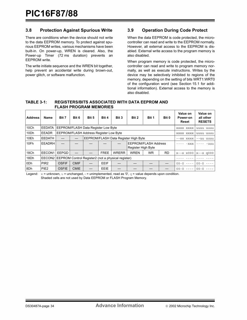
PIC16F87/88
3.8 Protection Against Spurious WriteThere are conditions when the device should not writeto the data EEPROM memory. To protect against spu-rious EEPROM writes, various mechanisms have beenbuilt-in. On power-up, WREN is cleared. Also, thePower-up Timer (72 ms duration) prevents anEEPROM write.The write initiate sequence and the WREN bit together,help prevent an accidental write during brown-out,power glitch, or software malfunction.
3.9 Operation During Code ProtectWhen the data EEPROM is code protected, the micro-controller can read and write to the EEPROM normally.However, all external access to the EEPROM is dis-abled. External write access to the program memory isalso disabled.
When program memory is code protected, the micro-controller can read and write to program memory nor-mally, as well as execute instructions. Writes by thedevice may be selectively inhibited to regions of thememory, depending on the setting of bits WRT1:WRT0of the configuration word (see Section 15.1 for addi-tional information). External access to the memory isalso disabled.
TABLE 3-1: REGISTERS/BITS ASSOCIATED WITH DATA EEPROM AND FLASH PROGRAM MEMORIES
Address Name Bit 7 Bit 6 Bit 5 Bit 4 Bit 3 Bit 2 Bit 1 Bit 0Value on Power-on
Reset
Value on all other RESETS
10Ch EEDATA EEPROM/FLASH Data Register Low Byte xxxx xxxx uuuu uuuu
10Dh EEADR EEPROM/FLASH Address Register Low Byte xxxx xxxx uuuu uuuu
10Eh EEDATH — — EEPROM/FLASH Data Register High Byte --xx xxxx --uu uuuu
10Fh EEADRH — — — — — EEPROM/FLASH Address Register High Byte
---- -xxx ---- -uuu
18Ch EECON1 EEPGD — — FREE WRERR WREN WR RD x--x x000 x--x q000
18Dh EECON2 EEPROM Control Register2 (not a physical register) ---- ---- ---- ----
0Dh PIR2 OSFIF CMIF — EEIF — — — — 00-0 ---- 00-0 ----
8Dh PIE2 OSFIE CMIE — EEIE — — — — 00-0 ---- 00-0 ----
Legend: x = unknown, u = unchanged, - = unimplemented, read as '0', q = value depends upon condition. Shaded cells are not used by Data EEPROM or FLASH Program Memory.
DS30487A-page 34 Advance Information 2002 Microchip Technology Inc.

PIC16F87/88
4.0 OSCILLATOR CONFIGURATIONS
4.1 Oscillator TypesThe PIC16F87/88 can be operated in eight differentOscillator modes. The user can program three configu-ration bits (FOSC2:FOSC0) to select one of these eightmodes (modes 5 - 8 are new PIC16 oscillatorconfigurations):
1. LP Low Power Crystal2. XT Crystal/Resonator3. HS High Speed Crystal/Resonator4. RC External Resistor/Capacitor with
FOSC/4 output on RA65. RCIO External Resistor/Capacitor with
I/O on RA66. INTIO1 Internal Oscillator with FOSC/4
output on RA6 and I/O on RA77. INTIO2 Internal Oscillator with I/O on RA6
and RA78. ECIO External Clock with I/O on RA6
4.2 Crystal Oscillator/Ceramic Resonators
In XT, LP or HS modes, a crystal or ceramic resonatoris connected to the OSC1/CLKI and OSC2/CLKO pinsto establish oscillation (see Figure 4-1 and Figure 4-2).The PIC16F87/88 oscillator design requires the use ofa parallel cut crystal. Use of a series cut crystal maygive a frequency out of the crystal manufacturersspecifications.
FIGURE 4-1: CRYSTAL OPERATION (HS, XT, OR LP OSC CONFIGURATION)
TABLE 4-1: CAPACITOR SELECTION FOR CRYSTAL OSCILLATOR(FOR DESIGN GUIDANCE ONLY)
Note 1: See Table 4-1 for typical values of C1 andC2.
2: A series resistor (RS) may be required for ATstrip cut crystals.
3: RF varies with the crystal chosen (typicallybetween 2 MΩ to 10 MΩ).
C1(1)
C2(1)
XTAL
OSC2
RS(2)
OSC1
RF(3) SLEEP
To Internal Logic
PIC16F87/88
Osc Type Crystal Freq
Typical Capacitor Values Tested:
C1 C2
LP 32 kHz 33 pF 33 pF200 kHz 15 pF 15 pF
XT 200 kHz 56 pF 56 pF1 MHz 15 pF 15 pF4 MHz 15 pF 15 pF
HS 4 MHz 15 pF 15 pF8 MHz 15 pF 15 pF
20 MHz 15 pF 15 pFCapacitor values are for design guidance only. These capacitors were tested with the crystals listedbelow for basic start-up and operation. These valueswere not optimized.
Different capacitor values may be required to produceacceptable oscillator operation. The user should testthe performance of the oscillator over the expectedVDD and temperature range for the application.
See the notes following this table for additionalinformation.
Note 1: Higher capacitance increases the stabilityof oscillator, but also increases thestart-up time.
2: Since each crystal has its own character-istics, the user should consult the crystalmanufacturer for appropriate values ofexternal components.
3: Rs may be required in HS mode, as wellas XT mode, to avoid overdriving crystalswith low drive level specification.
4: Always verify oscillator performance overthe VDD and temperature range that isexpected for the application.
2002 Microchip Technology Inc. Advance Information DS30487A-page 35

PIC16F87/88
FIGURE 4-2: CERAMIC RESONATOROPERATION (HS OR XT OSC CONFIGURATION)
TABLE 4-2: CERAMIC RESONATORS(FOR DESIGN GUIDANCE ONLY)
4.3 External Clock InputThe ECIO Oscillator mode requires an external clocksource to be connected to the OSC1 pin. There is nooscillator start-up time required after a Power-onReset, or after an exit from SLEEP mode.
In the ECIO Oscillator mode, the OSC2 pin becomesan additional general purpose I/O pin. The I/O pinbecomes bit 6 of PORTA (RA6). Figure 4-3 shows thepin connections for the ECIO Oscillator mode.
FIGURE 4-3: EXTERNAL CLOCK INPUT OPERATION (ECIO CONFIGURATION)
Typical Capacitor Values Used:
Mode Freq OSC1 OSC2
XT 455 kHz2.0 MHz4.0 MHz
56 pF47 pF33 pF
56 pF47 pF33 pF
HS 8.0 MHz16.0 MHz
27 pF22 pF
27 pF22 pF
Capacitor values are for design guidance only. These capacitors were tested with the resonatorslisted below for basic start-up and operation. Thesevalues were not optimized.
Different capacitor values may be required to produceacceptable oscillator operation. The user should testthe performance of the oscillator over the expectedVDD and temperature range for the application.
See the notes following this table for additionalinformation.
Note: When using resonators with frequenciesabove 3.5 MHz, the use of HS mode,rather than XT mode, is recommended. HSmode may be used at any VDD for whichthe controller is rated. If HS is selected, it ispossible that the gain of the oscillator willoverdrive the resonator. Therefore, aseries resistor should be placed betweenthe OSC2 pin and the resonator. As a goodstarting point, the recommended value ofRS is 330Ω.
Note 1: See Table 4-2 for typical values of C1 andC2.
2: A series resistor (RS) may be required.3: RF varies with the resonator chosen
(typically between 2 MΩ to 10 MΩ).
C1(1)
C2(1)
RES
OSC2
RS(2)
OSC1
RF(3) SLEEP
To Internal Logic
PIC16F87/88
OSC1/CLKI
I/O (OSC2)RA6
Clock fromExt. System PIC16F87/88
DS30487A-page 36 Advance Information 2002 Microchip Technology Inc.

PIC16F87/88
4.4 RC OscillatorFor timing insensitive applications, the “RC” and“RCIO” device options offer additional cost savings.The RC oscillator frequency is a function of the supplyvoltage, the resistor (REXT) and capacitor (CEXT) val-ues, and the operating temperature. In addition to this,the oscillator frequency will vary from unit to unit due tonormal manufacturing variation. Furthermore, the dif-ference in lead frame capacitance between packagetypes will also affect the oscillation frequency, espe-cially for low CEXT values. The user also needs to takeinto account variation due to tolerance of external Rand C components used. Figure 4-4 shows how theR/C combination is connected.In the RC Oscillator mode, the oscillator frequencydivided by 4 is available on the OSC2 pin. This signal maybe used for test purposes or to synchronize other logic.
FIGURE 4-4: RC OSCILLATOR MODE
The RCIO Oscillator mode (Figure 4-5) functions likethe RC mode, except that the OSC2 pin becomes anadditional general purpose I/O pin. The I/O pinbecomes bit 6 of PORTA (RA6).
FIGURE 4-5: RCIO OSCILLATOR MODE
4.5 Internal Oscillator BlockThe PIC16F87/88 devices include an internal oscillatorblock, which generates two different clock signals;either can be used as the system’s clock source. Thiscan eliminate the need for external oscillator circuits onthe OSC1 and/or OSC2 pins.
The main output (INTOSC) is an 8 MHz clock source,which can be used to directly drive the system clock. Italso drives the INTOSC postscaler, which can providea range of six clock frequencies from 125 kHz to4 MHz.
The other clock source is the internal RC oscillator(INTRC), which provides a 31.25 kHz (32 µs nominalperiod) output. The INTRC oscillator is enabled byselecting the INTRC as the system clock source, orwhen any of the following are enabled:
• Power-up Timer • Watchdog Timer• Two-Speed Start-up• Fail-Safe Clock MonitorThese features are discussed in greater detail inSection 15.0 (“Special Features of the CPU”).
The clock source frequency (INTOSC direct, INTRCdirect, or INTOSC postscaler) is selected by configuringthe IRCF bits of the OSCCON register (page 41).
OSC2/CLKO
CEXT
REXT
PIC16F87/88
OSC1
FOSC/4
InternalClock
VDD
VSS
Recommended values: 3 kΩ ≤ REXT ≤ 100 kΩCEXT > 20 pF
CEXT
REXT
PIC16F87/88
OSC1 InternalClock
VDD
VSS
Recommended values: 3 kΩ ≤ REXT ≤ 100 kΩCEXT > 20 pF
I/O (OSC2)RA6
Note: Throughout this data sheet, when referringspecifically to a generic clock source, theterm “INTRC” may also be used to refer tothe Clock modes using the internal oscilla-tor block. This is regardless of whether theactual frequency used is INTOSC (8 MHz),the INTOSC postscaler, or INTRC(31.25 kHz).
2002 Microchip Technology Inc. Advance Information DS30487A-page 37

PIC16F87/88
4.5.1 INTRC MODESUsing the internal oscillator as the clock source caneliminate the need for up to two external oscillator pins,after which it can be used for digital I/O. Two distinctconfigurations are available:
• In INTIO1 mode, the OSC2 pin outputs FOSC/4, while OSC1 functions as RA7 for digital input and output.
• In INTIO2 mode, OSC1 functions as RA7 and OSC2 functions as RA6, both for digital input and output.
4.5.2 OSCTUNE REGISTER
The internal oscillator’s output has been calibrated at thefactory, but can be adjusted in the application. This isdone by writing to the OSCTUNE register (Register 4-1).The tuning sensitivity is constant throughout the tuningrange. See Section 18.0 (“Electrical Characteristics”) forfurther details.
When the OSCTUNE register is modified, the INTRCfrequency will begin shifting to the new frequency. TheINTRC clock will reach the new frequency within 8 clockcycles (approximately 8 * 32 µs = 256 µs). Code execu-tion continues during this shift. There is no indication thatthe shift has occurred. Operation of features that dependon the 31.25 kHz INTRC clock source frequency, suchas the WDT and peripherals, will also be affected by thechange in frequency.
REGISTER 4-1: OSCTUNE: OSCILLATOR TUNING REGISTER U-0 U-0 R/W-0 R/W-0 R/W-0 R/W-0 R/W-0 R/W-0 — — TUN5 TUN4 TUN3 TUN2 TUN1 TUN0
bit 7 bit 0
bit 7-6 Unimplemented: Read as ‘0’bit 5-0 TUN<5:0>: Frequency Tuning bits
011111 = Maximum frequency011110 = •••000001 = 000000 = Center frequency. Oscillator Module is running at the calibrated frequency.111111 = •••100000 = Minimum frequency
Legend:R = Readable bit W = Writable bit U = Unimplemented bit, read as ‘0’-n = Value at POR ‘1’ = Bit is set ‘0’ = Bit is cleared x = Bit is unknown
DS30487A-page 38 Advance Information 2002 Microchip Technology Inc.

PIC16F87/88
4.6 Clock Sources and OscillatorSwitchingThe PIC16F87/88 devices include a feature that allowsthe system clock source to be switched from the mainoscillator to an alternate low frequency clock source.PIC16F87/88 devices offer three alternate clocksources. When enabled, these give additional optionsfor switching to the various Power Managed Operatingmodes.
Essentially, there are three clock sources for thesedevices:
• Primary oscillators• Secondary oscillators• Internal oscillator block (INTRC)
The primary oscillators include the external Crystaland Resonator modes, the external RC modes, theexternal Clock mode and the internal oscillator block.The particular mode is defined on POR by the contentsof Configuration Word 1. The details of these modesare covered earlier in this chapter.
The secondary oscillators are those external sourcesnot connected to the OSC1 or OSC2 pins. Thesesources may continue to operate even after thecontroller is placed in a Power Managed mode.
PIC16F87/88 devices offer only the Timer1 oscillator asa secondary oscillator. This oscillator continues to runwhen a SLEEP instruction is executed, and is often thetime-base for functions, such as a real-time clock.
Most often, a 32.768 kHz watch crystal is connectedbetween the RB6/T1OS0 and RB7/T1OSI pins. Likethe LP mode oscillator circuit, loading capacitors arealso connected from each pin to ground. The Timer1oscillator is discussed in greater detail in Section 7.6.
In addition to being a primary clock source, the internaloscillator block is available as a Power Managedmode clock source. The 31.25 kHz INTRC source isalso used as the clock source for several special fea-tures, such as the WDT, Fail-Safe Clock Monitor,Power-up Timer, and Two-Speed Start-up.
The clock sources for the PIC16F87/88 devices areshown in Figure 4-6. See Section 7.0 for further detailsof the Timer1 oscillator. See Section 15.1 forConfiguration register details.
4.6.1 OSCILLATOR CONTROL REGISTER
The OSCCON register (Register 4-2) controls severalaspects of the system clock’s operation, both in fullpower operation and in Power Managed modes.
The System Clock Select bits, SCS1:SCS0, select theclock source that is used when the device is operatingin Power Managed modes. When the bits arecleared (= 00), the system clock source comes fromthe main oscillator that is selected by theFOSC2:FOSC0 configuration bits in ConfigurationRegister 1. When the bits are set in any other manner,the system clock source is provided by the Timer1oscillator (SCS1:SCS0 = 01), or from the internal oscil-lator block (SCS1:SCS0 = 10). After a RESET,SCS<1:0> are always set to ‘00’.
The Internal Oscillator Select bits, IRCF2:IRCF0, selectthe frequency output of the internal oscillator block thatis used to drive the system clock. The choices are theINTRC source (31.25 kHz), the INTOSC source(8 MHz), or one of the six frequencies derived from theINTOSC postscaler (125 kHz to 4 MHz). Changing theconfiguration of these bits has an immediate change onthe internal oscillator’s output.
The OSTS and IOFS bits indicate the status of the pri-mary oscillator and INTOSC source; these bits are setwhen their respective oscillators are stable. In particu-lar, OSTS indicates that the Oscillator Start-up Timerhas timed out.
2002 Microchip Technology Inc. Advance Information DS30487A-page 39

PIC16F87/88
FIGURE 4-6: PIC16F87/88 CLOCK DIAGRAM4.6.2 MODIFYING THE IRCF BITS
The IRCF bits can be modified at any time, regardlessof which clock source is currently being used as the sys-tem clock. The internal oscillator allows users to changethe frequency during RUN time. This is achieved bymodifying the IRCF bits in the OSCCON register. Thesequence of events that occur after the IRCF bits aremodified is dependent upon the initial value of the IRCFbits before they are modified. The system clock, ineither case, will switch to the new internal oscillator fre-quency after eight falling edges of the new clock. If theINTRC (31.25 kHz) is running and the IRCF bits aremodified to any of the other high frequency values, a1 ms clock switch delay is turned on. Code executioncontinues at a higher than expected frequency while thenew frequency stabilizes. Time sensitive code shouldwait for the IOFS bit in the OSCCON register to becomeset before continuing. This bit can be monitored toensure that the frequency is stable before using thesystem clock in time critical applications.
If the IRCF bits are modified while the internal oscillatoris running at any other frequency than INTRC(31.25 kHz), there is no need for a 1 ms clock switchdelay. The new INTOSC frequency will be stable imme-diately after the eight falling edges. The IOFS bit willremain set after clock switching occurs.
Caution must be taken when modifying the IRCF bitsusing BCF or BSF instructions. It is possible to modifythe IRCF bits to a frequency that may be out of the VDDspecification range; for example, VDD = 2.0V andIRCF = 111 (8 MHz).
4.6.3 CLOCK TRANSITION SEQUENCE WHEN THE IRCF BITS ARE MODIFIED
The following sequence is performed when the IRCFbits are changed and the system clock is the internaloscillator.
1. The IRCF bits are modified.2. The clock switching circuitry waits for a falling
edge of the current clock, at which point CLKOis held low.
3. The clock switching circuitry then waits for eightfalling edges of requested clock, after which itswitches CLKO to this new clock source.
4. If the INTRC (31.25 kHz) is enabled, the IOFSbit is clear to indicate that the clock is unstableand a 1 ms delay is started. If the internal oscil-lator frequency is anything other than INTRC(31.25 kHz), this step is skipped. After theappropriate number of clock periods havepassed, the IOFS bit is set to indicate to theinternal oscillator that the frequency is stable.
5. Oscillator switch over is complete.
Secondary Oscillator
T1OSCENEnableOscillator
T1OSO
T1OSI
OSC1
OSC2
SLEEP
Primary Oscillator
LP, XT, HS, RC, EC
T1OSC
CPU
Peripherals
Pos
tsca
ler
MU
X
MU
X
8 MHz
4 MHz
2 MHz
1 MHz
500 kHz
125 kHz
250 kHz
OSCCON<6:4>
11111010110001101000100031.25 kHz
31.25 kHzSource
InternalOscillator
Block
WDT, FSCM31.25 kHz
8 MHz
Internal Oscillator
(INTRC)
(INTOSC)
Config1(FOSC2:FOSC0)SCS<1:0>(T1OSC)
DS30487A-page 40 Advance Information 2002 Microchip Technology Inc.

PIC16F87/88
REGISTER 4-2: OSCCON: OSCILLATOR CONTROL REGISTERU-0 R/W-0 R/W-0 R/W0 R-0 R-0 R-0 R-0 — IRCF2 IRCF1 IRCF0 OSTS IOFS SCS1 SCS0
bit 7 bit 0
bit 7 Unimplemented: Read as ‘0’bit 6-4 IRCF<2:0>: Internal RC Oscillator Frequency Select bits
000 = 31.25 kHz001 = 125 kHz010 = 250 kHz011 = 500 kHz100 = 1 MHz101 = 2 MHz110 = 4 MHz111 = 8 MHz
bit 3 OSTS: Oscillator Start-up Time-out Status bit1 = Device is running from the primary system clock0 = Device is running from T1OSC or INTRC as a secondary system clock
bit 2 IOFS: INTOSC Frequency Stable bit1 = Frequency is stable0 = Frequency is not stable
bit 1-0 SCS<1:0>: Oscillator Mode Select bits00 = Oscillator mode defined by FOSC<2:0>01 = T1OSC is used for system clock10 = Internal RC is used for system clock11 = Reserved
Legend:R = Readable bit W = Writable bit U = Unimplemented bit, read as ‘0’-n = Value at POR ‘1’ = Bit is set ‘0’ = Bit is cleared x = Bit is unknown
2002 Microchip Technology Inc. Advance Information DS30487A-page 41

PIC16F87/88
4.6.4 OSCILLATOR DELAY UPONPOWER-UP AND WAKE-UP
The Oscillator Start-up Timer (OST) is used to ensurethat a stable system clock is provided to the device.The OST is activated following a POR, or a wake-upfrom SLEEP mode, when the system clock is config-ured for one of the primary oscillator modes (LP, XT,and HS).
Table 4-3 shows examples where the oscillator delay isinvoked.
TABLE 4-3: OSCILLATOR DELAY EXAMPLESSwitch From Switch To Frequency Oscillator Delay Comments
SLEEP INTRCT1OSC
31.25 kHz32.768 kHz
5 µs - 10 µs (approx.) CPU Start-up(1)
Following a wake-up from SLEEP mode or POR, CPU start-up is invoked to allow the CPU to become ready for code execution.
SLEEP INTOSC 125 kHz - 8 MHzINTRC/SLEEP EC, RC 0 - 20 MHz
INTRC (31.25 kHz)
EC, RC 0 - 20 MHz
SLEEP LP, XT, HS 32.768 kHz - 20 MHz 1024 Clock Cycles (OST)
Following a change from INTRC, an OST of 1024 cycles must occur.
INTRC (31.25 kHz)
INTOSC 125 kHz - 8 MHz 1 ms Refer to Section 4.6.2 for further details.
Note 1: The 5 µs - 10 µs start-up delay is based on a 1 MHz System Clock.
DS30487A-page 42 Advance Information 2002 Microchip Technology Inc.

PIC16F87/88
4.6.5 CLOCK SWITCHINGClock switching will occur for the following reasons:
• The FCMEN bit is set, the device is running from the primary oscillator, and the primary oscillator fails.
• The FCMEN bit is set, the device is running from the T1OSC and T1OSC fails.
• Following a wake-up due to a RESET or a POR, when the device is configured for Two-Speed mode, switching will occur between the INTRC and the system clock defined by the FOSC<2:0> bits.
• A wake-up from SLEEP occurs due to interrupt or WDT wake-up and Two-Speed Start-up is enabled. If the primary clock is XT, HS, or LP, the clock will switch between the INTRC and the pri-mary system clock after 1024 clock (OST) and 8 clocks of the primary oscillator. This is conditional upon the SCS bits being set equal to ‘00’.
4.6.6 CLOCK TRANSITION DELAYS
When a clock transition is requested, the CLKO signalwill continue to provide the current clock at its outputthroughout the transition period. After this transitionperiod, the requested clock will start to drive the CLKOsignal. The transition delay comprises the time todetect clock source stability plus eight cycles (of thenew clock). For internal RC oscillators, the transitiondelay is eight clocks. When the Primary oscillator isconfigured for any oscillator (LP, XT, or HS), the transi-tion delay is 1024 plus eight clocks. When the primaryoscillator is configured for an external clock, thetransition delay is eight clocks.
If an attempt is made to switch to the same clocksource already in use, the clock transition sequencewill not take place.
4.6.7 CLOCK TRANSITION AND THE WATCHDOG
When clock switching is performed, the WatchdogTimer is disabled because the Watchdog RippleCounter is used as the Oscillator Start-up Timer.
Once the clock transition is complete (i.e., new oscilla-tor selection switch has occurred), the WatchdogCounter is re-enabled with the Counter Reset. Thisallows the user to synchronize the Watchdog Timer tothe start of execution at the new clock frequency.
Note: Because the SCS bits are cleared on anyRESET, no clock switching will occur on aRESET unless the Two-Speed Start-up isenabled and the primary clock is XT, HS, orLP. The device will wait for the primaryclock to become stable before executionbegins (Two-Speed Start-up disabled).
Note: The OST is only used when switching toXT, HS, and LP Oscillator modes.
2002 Microchip Technology Inc. Advance Information DS30487A-page 43

PIC16F87/88
4.7 Power Managed Modes4.7.1 RC_RUN MODE
When SCS bits are configured to run from the INTRC,a clock transition is generated if the system clock isnot already using the INTRC. The event will clear theOSTS bit, switch the system clock from the primarysystem clock (if SCS<1:0> = 00) determined by thevalue contained in the configuration bits, or from theT1OSC (if SCS<1:0> = 01) to the INTRC clock option,and shut down the primary system clock to conservepower. Clock switching will not occur if the primarysystem clock is already configured as INTRC.
If the system clock does not come from the INTRC(31.25 kHz) when the SCS bits are changed, and theIRCF bits in the OSCCON register are configured for afrequency other than INTRC, the frequency may notbe stable immediately. The IOFS bit (OSCCON<2>)will be set when the INTOSC or postscaler frequencyis stable, after approximately 1 ms.
After a clock switch has been executed, the OSTS bitis cleared, indicating a Low Power mode, and thedevice does not run from the primary system clock.The internal Q clocks are held in the Q1 state untileight falling edge clocks are counted on the INTRCoscillator. After the eight clock periods have tran-spired, the clock input to the Q clocks is released andoperation resumes (see Figure 4-7).
FIGURE 4-7: TIMING DIAGRAM FOR XT, HS, LP, EC AND EXTRC TO RC_RUN MODE
Q4Q3Q2
OSC1
SCS<1:0>
Program PC + 1PC
Note 1: TINP = 32 µs typical.2: TOSC = 50 ns minimum.3: TSCS = 8 TINP.4: TDLY = 1 TINP.
Q1
INTOSC
Q1
TSCS(3)
Counter
Q1
TDLY(4)
TINP(1)
SystemClock
TOSC(2)
Q3Q2 Q4 Q1 Q2
PC +2 PC + 3
Q3 Q4 Q1
DS30487A-page 44 Advance Information 2002 Microchip Technology Inc.

PIC16F87/88
4.7.2 SEC_RUN MODEThe core and peripherals can be configured to beclocked by T1OSC using a 32.768 kHz crystal. Thecrystal must be connected to the T1OSO and T1OSIpins. This is the same configuration as the low powertimer circuit (see Section 7.6). When SCS bits are con-figured to run from T1OSC, a clock transition is gener-ated. It will clear the OSTS bit, switch the system clockfrom either the primary system clock, or INTRC,depending on the value of SCS<1:0> andFOSC<2:0>, to the external low power Timer1 oscilla-tor input (T1OSC), and shut down the primary systemclock to conserve power.
After a clock switch has been executed, the internal Qclocks are held in the Q1 state until eight falling edgeclocks are counted on the T1OSC. After the eightclock periods have transpired, the clock input to the Qclocks is released and operation resumes (seeFigure 4-8). In addition, T1RUN (In T1CON) is set toindicate that T1OSC is being used as the systemclock.
FIGURE 4-8: TIMING DIAGRAM FOR SWITCHING TO SEC_RUN MODE
Note 1: The T1OSCEN bit must be enabled and itis the user’s responsibility to ensureT1OSC is stable before clock switching tothe T1OSC input clock can occur.
2: When T1OSCEN = 0, the following possibleeffects result.
OriginalSCS<1:0>
ModifiedSCS<1:0>
FinalSCS<1:0>
00 01 00 - no change00 11 10 - INTRC10 11 10 - no change10 01 00 - OSC
defined by FOSC<2:0>
A clock switching event will occur if thefinal state of the SCS bits is different fromthe original.
Q4Q3Q2
OSC1
SCS<1:0>
Program PC +1PC
Note 1: TT1P = 30.52 µs.2: TOSC = 50 ns minimum.3: TSCS = 8 TT1P 4: TDLY = 1 TT1P.
Q1
T1OSI
Q1
TSCS(3)
Counter
Q1
TDLY(4)
TT1P(1)
SystemClock
TOSC(2)
Q3Q2 Q4 Q1 Q2
PC + 2 PC +3
Q3 Q4 Q1
2002 Microchip Technology Inc. Advance Information DS30487A-page 45

PIC16F87/88
4.7.3 SEC_RUN/RC_RUN TO PRIMARYCLOCK SOURCE
When switching from a SEC_RUN or RC_RUN modeback to the primary system clock, following a changeof SCS<1:0> to ‘00’, the sequence of events that takeplace will depend upon the value of the FOSC bits inthe Configuration register. If the external oscillator isconfigured as a crystal (HS, XT, or LP), then the transi-tion will take place after 1024 clock cycles. This is nec-essary because the crystal oscillator had beenpowered down until the time of the transition. In orderto provide the system with a reliable clock when thechangeover has occurred, the clock will not bereleased to the changeover circuit until the 1024 counthas expired.
During the Oscillator Start-up Time, the system clockcomes from the current system clock. Instruction exe-cution and/or peripheral operation continues using thecurrently selected oscillator as the CPU clock source,until the necessary clock count has expired to ensurethat the primary system clock is stable.
Following the Oscillator Start-up Time, the internal Qclocks are held in the Q1 state until eight falling edgeclocks are counted from the primary system clock. Theclock input to the Q clocks is then released, and oper-ation resumes with primary system clock determinedby the FOSC bits (see Figure 4-10).
4.7.3.1 Returning to Primary Clock Source Sequence
Changing back to the primary oscillator fromSEC_RUN or RC_RUN can be accomplished by eitherchanging SCS<1:0> to ‘00’, or clearing the T1OSCENbit in the T1CON register (if T1OSC was the secondaryclock).
The sequence of events that follows is the same forboth modes:
1. If the primary system clock is configured as EC,RC, or INTRC, then the OST time-out isskipped. Skip to step 3.
2. If the primary system clock is configured as anexternal oscillator (HS, XT, LP), then the OSTwill be active, waiting for 1024 clocks of theprimary system clock.
3. On the following Q1, the device holds thesystem clock in Q1.
4. The device stays in Q1 while eight falling edgesof the primary system clock are counted.
5. Once the eight counts transpire, the devicebegins to run from the primary oscillator.
6. If the secondary clock was INTRC and the pri-mary is not INTRC, the INTRC will be shut downto save current, providing that the INTRC is notbeing used for any other function, such as WDT,or Fail-Safe Clock Monitoring.
7. If the secondary clock was T1OSC, the T1OSCwill continue to run if T1OSCEN is still set,otherwise the T1 oscillator will be shut down.
Note 1: When the device is configured to useT1OSC, the act of clearing the T1OSCENbit in the T1CON register will causeSCS<0> to be cleared, which causes theSCS<1:0> bits to revert to ‘00’ or ‘10’,depending on what SCS<1> is. TheT1OSCEN bit will be cleared immediately;however, T1OSC will be enabled andinstruction execution will continue untilthe OST time-out for the main systemclock is complete. At that time, the systemclock will switch from the T1OSC to theprimary clock or the INTRC. Followingthis, the T1 oscillator will be shut down.
2: If it is desired not to run time critical appli-cation code while running from the sec-ondary clock source, the OSTS bit shouldbe monitored until the Oscillator Start-upTimer has completed. OSTS = 1 indicatesthat the Oscillator Start-up Timer hastimed out and the system clock comesfrom the primary clock source.
Note: If the primary system clock is either RC orEC, an internal delay timer (5 - 10 µs) willsuspend operation after exiting SecondaryClock mode to allow the CPU to becomeready for code execution.
DS30487A-page 46 Advance Information 2002 Microchip Technology Inc.

PIC16F87/88
FIGURE 4-9: TIMING FOR TRANSITION BETWEEN SEC_RUN/RC_RUN AND PRIMARYCLOCK
Q4 Q1 Q3 Q4
OSC1
Program PC PC + 1
Sec. Osc
Primary Clock
TOST(6)
Q1
PC +3
TOSC(3)
TDLY(5)
TT1P(1) or TINP(2)
TSCS(4)
Q2
OSC2
Q3 Q4 Q1
OSTS
System Clock
PC + 2Counter
Q2 Q2 Q3 Q4
SCS<1:0>
Note 1: TT1P = 30.52 µs.2: TINP = 32 µs typical.3: TOSC = 50 ns minimum.4: TSCS = 8 TINP OR 8 TT1P.5: TDLY = 1 TINP OR 1 TT1P.6: Refer to parameter “D033” in Section 18.0.
2002 Microchip Technology Inc. Advance Information DS30487A-page 47

PIC16F87/88
4.7.3.2 Returning to Primary Oscillator witha RESETA RESET will clear SCS<1:0> back to ‘00’. Thesequence for starting the primary oscillator following aRESET is the same for all forms of RESET, includingPOR. There is no transition sequence from the sec-ondary system clock to the primary system clock.Instead, the device will reset the state of the OSCCONregister and default to the primary system clock. Thesequence of events that take place after this willdepend upon the value of the FOSC bits in the Config-uration register. If the external oscillator is configuredas a crystal (HS, XT, or LP), the CPU will be held in theQ1 state until 1024 clock cycles have transpired on theprimary clock. This is necessary because the crystaloscillator had been powered down until the time of thetransition.
During the Oscillator Start-up Time, the system clockdoes not come from the low power oscillator. Instruc-tion execution and/or peripheral operation is sus-pended and the secondary, low power, oscillator isdisabled.
If the primary system clock is either RC, EC, orINTRC, the CPU will begin operating on the first Q1cycle following the wake-up event. This means thatthere is no Oscillator Start-up Time required becausethe primary clock is already stable; however, there is a
delay between the wake-up event and the followingQ2. An internal delay timer of 5 - 10 µs will suspendoperation after the RESET to allow the CPU tobecome ready for code execution. The CPU andperipheral clock will be held in the first Q1 following theexit from low power. The clocks will be released on thenext falling edge of the input system clock. The CPUwill advance the system clock into the Q2 state follow-ing two rising edges of the incoming clock on OSC1.The extra clock transition is required following aRESET to allow the system clock to synchronize to theasynchronous nature of the RESET source (seeFigure 4-11).
The sequence of events is as follows:
1. A device RESET is asserted from one of manysources (WDT, BOR, MCLR, etc.).
2. The device resets and the CPU start-up timer isenabled if in SLEEP mode. The device is held inRESET until the CPU start-up time-out iscomplete.
3. If the primary system clock is configured as anexternal oscillator (HS, XT, LP), then the OSTwill be active waiting for 1024 clocks of the pri-mary system clock. While waiting for the OST,the device will be held in RESET. The OST andCPU start-up timers run in parallel.
4. After both the CPU start-up and OST timershave timed out, the device will wait for one addi-tional clock cycle and instruction execution willbegin.
FIGURE 4-10: TIMING LP CLOCK TO PRIMARY SYSTEM CLOCK AFTER RESET (HS, XT, LP)
Note: If Two-Speed Clock Start-up mode isenabled, the INTRC will act as the systemclock until the OST timer has timed out.
Q4 Q1 Q3 Q4 Q1 Q2
OSC1
Peripheral
SLEEP
Program PC 0000h
T1OSI
TOST(4)
Q3
TOSC(2)
TT1P(1)
Q4
OSC2
OSTS
System Clock
0001h
Q1 Q2 Q3 Q4 Q1 Q2
Clock
Counter 0004h 0005h0003h
Q1 Q2 Q3 Q4
RESET
TCPU(3)
Note 1: TT1P = 30.52 µs.2: TOSC = 50 ns minimum.3: TCPU = 5 - 10 µs (1 MHz System Clock).4: Refer to parameter “D033” in Section 18.0.
CPU Start-up
DS30487A-page 48 Advance Information 2002 Microchip Technology Inc.

PIC16F87/88
FIGURE 4-11: TIMING LP CLOCK TO PRIMARY SYSTEM CLOCK AFTER RESET (EC, RC, INTRC)Q4 Q1 Q3 Q4 Q1 Q2
OSC1
Program PC 0000h
T1OSI
Q3
TT1P(1)
Q4
OSC2
OSTS
System Clock
0001h
Q1 Q2 Q3 Q4 Q1 Q2
Counter 0003h 0004h0002h
Q1 Q2 Q3 Q4
MCLR
TCPU(2)
Note 1: TT1P = 30.52 µs.2: TCPU = 5 - 10 µs (1 MHz System Clock).
CPU Start-up
2002 Microchip Technology Inc. Advance Information DS30487A-page 49

PIC16F87/88
TABLE 4-4: CLOCK SWITCHING MODES
Current System Clock
SCS bits <1:0>Modified to:
OSTSbit Delay IOFS
bitT1RUN
bit
New System Clock
Comments
LP, XT, HS,T1OSC,EC, RC
10(INTRC)
0 8 Clocks of INTRC
1 0 INTRCor
INTOSCor
INTOSC Postscaler
The internal RC oscillator frequency is dependant upon the IRCF bits.
LP, XT, HS,INTRC,EC, RC
01(T1OSC)
0 8 Clocks of T1OSC
N/A 1 T1OSC T1OSCEN bit must be enabled.
INTRCT1OSC
00FOSC<2:0> = EC
orFOSC<2:0> = RC
1 8 Clocks of ECor
RC
N/A 0 ECor
RC
INTRCT1OSC
00FOSC<2:0> = LP,
XT, HS
0 1024 Clocks(OST)
+8 Clocks of LP, XT, HS
N/A 0 LP, XT, HS During the 1024 clocks, program execution is clocked from the second-ary oscillator until the primary oscillator becomes stable.
LP, XT, HS 00(Due to RESET)
LP, XT, HS
1 1024 Clocks(OST)
N/A 0 LP, XT, HS When a RESET occurs, there is no clock transition sequence.Instruction execution and/or peripheral opera-tion is suspended unless Two-Speed Start-up mode is enabled, after which the INTRC will act as the sys-tem clock until the OST timer has timed out.
DS30487A-page 50 Advance Information 2002 Microchip Technology Inc.
PIC16F87/88
4.7.4 EXITING SLEEP WITH ANINTERRUPT
Any interrupt, such as WDT or INT0, will cause the partto leave the SLEEP mode.
The SCS bits are unaffected by a SLEEP command andare the same before and after entering and leavingSLEEP. The clock source used after an exit fromSLEEP is determined by the SCS bits.
4.7.4.1 Sequence of EventsIf SCS<1:0> = 00:1. The device is held in SLEEP until the CPU
start-up time-out is complete.2. If the primary system clock is configured as an
external oscillator (HS, XT, LP), then the OSTwill be active waiting for 1024 clocks of the pri-mary system clock. While waiting for the OST,the device will be held in SLEEP unlessTwo-Speed Start-up is enabled. The OST andCPU start-up timers run in parallel. Refer toSection 15.12.4 for details on Two-SpeedStart-up.
3. After both the CPU start-up and OST timershave timed out, the device will exit SLEEP andbegin instruction execution with the primaryclock defined by the FOSC bits.
If SCS<1:0> = 01 or 10:1. The device is held in SLEEP until the CPU
start-up time-out is complete.2. After the CPU start-up timer has timed out, the
device will exit SLEEP and begin instructionexecution with the selected Oscillator mode.
Note: If a user changes SCS<1:0> just beforeentering SLEEP mode, the system clockused when exiting SLEEP mode could bedifferent than the system clock used whenentering SLEEP mode.
As an example, if SCS<1:0> = 01 andT1OSC is the system clock, and the follow-ing instructions are executed:
BCF OSCON,SCS0
SLEEP
then a clock change event is executed. Ifthe primary oscillator is XS, LP, or HS, thecore will continue to run off T1OSC andexecute the SLEEP command.
When SLEEP is exited, the part will resumeoperation with the primary oscillator afterthe start-up.
2002 Microchip Technology Inc. Advance Information DS30487A-page 51

PIC16F87/88
NOTES:DS30487A-page 52 Advance Information 2002 Microchip Technology Inc.

PIC16F87/88
5.0 I/O PORTSSome pins for these I/O ports are multiplexed with analternate function for the peripheral features on thedevice. In general, when a peripheral is enabled, thatpin may not be used as a general purpose I/O pin.
Additional information on I/O ports may be found in thePICmicro™ Mid-Range Reference Manual (DS33023).
5.1 PORTA and the TRISA RegisterPORTA is a 8-bit wide, bi-directional port. The corre-sponding data direction register is TRISA. Setting aTRISA bit (= 1) will make the corresponding PORTA pinan input (i.e., put the corresponding output driver in aHi-Impedance mode). Clearing a TRISA bit (= 0) willmake the corresponding PORTA pin an output (i.e., putthe contents of the output latch on the selected pin).
Reading the PORTA register, reads the status of thepins, whereas writing to it, will write to the port latch. Allwrite operations are read-modify-write operations.Therefore, a write to a port implies that the port pins areread, this value is modified, and then written to the portdata latch.
Pin RA4 is multiplexed with the Timer0 module clockinput and with analog input to become the RA4/AN4/T0CKI/C2OUT pin. The RA4/AN4/T0CKI/C2OUT pin isa Schmitt Trigger input and full CMOS output driver.
Pin RA5 is multiplexed with the Master Clear moduleinput. The RA5/MCLR/VPP pin is a Schmitt Triggerinput.
Pin RA6 is multiplexed with the oscillator module inputand external oscillator output. Pin RA7 is multiplexedwith the oscillator module input and external oscillatorinput. Pin RA6/OSC2/CLKO and pin RA7/OSC1/CLKIare Schmitt Trigger inputs and full CMOS output drivers.
Pins RA<1:0> are multiplexed with analog inputs. PinsRA<3:2> are multiplexed with analog inputs, compara-tor outputs, and VREF inputs. Pins RA<3:0> have TTLinputs and full CMOS output drivers.
EXAMPLE 5-1: INITIALIZING PORTA
TABLE 5-1: PORTA FUNCTIONS
Note: On a Power-on Reset, the pinsPORTA<4:0> are configured as analoginputs and read as '0'.
BANKSEL PORTA ; select bank of PORTACLRF PORTA ; Initialize PORTA by
; clearing output; data latches
BANKSEL ADCON1 ; Select Bank of ADCON1MOVLW 0x06 ; Configure all pinsMOVWF ADCON1 ; as digital inputsMOVLW 0xFF ; Value used to
; initialize data ; direction
MOVWF TRISA ; Set RA<7:0> as inputs
Name Bit# Buffer Function
RA0/AN0 bit 0 TTL Input/output or analog input.RA1/AN1 bit 1 TTL Input/output or analog input.RA2/AN2/CVREF/VREF-(2)
bit 2 TTL Input/output or analog input or VREF- or Comparator VREF output.
RA3/AN3/VREF+(2)/C1OUT bit 3 TTL Input/output or analog input or VREF+ or Comparator output.RA4/AN4(2)/T0CKI/C2OUT bit 4 ST Input/output, analog input or TMR0 external input or
Comparator output.RA5/MCLR/VPP bit 5 ST Input, Master Clear (Reset) or Programming voltage input.RA6/OSC2/CLKO bit 6 ST Input/output, connects to Crystal or Resonator, Oscillator
output or 1/4 the frequency of OSC1, and denotes the instruction cycle in RC mode.
RA7/OSC1/CLKI bit 7 ST/CMOS(1) Input/output, connects to Crystal or Resonator or Oscillator input.
Legend: TTL = TTL input, ST = Schmitt Trigger inputNote 1: This buffer is a Schmitt Trigger input when configured in RC Oscillator mode and a CMOS input otherwise.
2: PIC16F88 only.
2002 Microchip Technology Inc. Advance Information DS30487A-page 53

PIC16F87/88
TABLE 5-2: SUMMARY OF REGISTERS ASSOCIATED WITH PORTAFIGURE 5-1: BLOCK DIAGRAM OF RA0/AN0:RA1/AN1 PINS
Address Name Bit 7 Bit 6 Bit 5 Bit 4 Bit 3 Bit 2 Bit 1 Bit 0 Value on POR, BOR
Value on all other RESETS
05h PORTA RA7 RA6 RA5 RA4 RA3 RA2 RA1 RA0 xxxx 0000(1)
xxx0 0000(2)uuuu 0000(1)
uuu0 0000(2)
85h TRISA TRISA7 TRISA6 TRISA5(3) PORTA Data Direction Register 1111 1111 1111 11119Fh ADCON1 ADFM ADCS2 VCFG1 VCFG0 — — — — 0000 ---- 0000 ----Legend: x = unknown, u = unchanged, - = unimplemented locations read as ‘0’. Shaded cells are not used by PORTA.Note 1: This value applies only to the PIC16F87.
2: This value applies only to the PIC16F88.3: Pin 5 is an input only; the state of the TRISA5 bit has no effect and will always read ‘1’.
DataBus QD
QCK P
N
WRPORTA
WRTRISA
Data Latch
TRIS Latch
RD TRISA
RD PORTA
AnalogVSS
VDD
I/O pinQD
QCK
Input Mode
DQ
EN
To Comparator
TTLInput Buffer
VDD
To A/D Module Channel Input (PIC16F88 only)
DS30487A-page 54 Advance Information 2002 Microchip Technology Inc.

PIC16F87/88
FIGURE 5-2: BLOCK DIAGRAM OF RA3/AN3/VREF+/C1OUT PINFIGURE 5-3: BLOCK DIAGRAM OF RA2/AN2/CVREF/VREF- Pin
DataBus QD
QCK
N
WRPORTA
WRTRISA
Data Latch
TRIS Latch
RD TRISA
RD PORTA
VSS
RA3 pinQD
QCK
DQ
EN
To A/D Module Channel Input (PIC16F88 only)
Schmitt TriggerInput Buffer
Comparator 1 Output
Comparator Mode = 110
VDD
AnalogInput Mode
To A/D Module Channel VREF+ Input (PIC16F88 only)
P
VDD
To Comparator
VSS
DataBus QD
QCK P
N
WRPORTA
WRTRISA
Data Latch
TRIS Latch
RD TRISA
RD PORTA
AnalogVSS
VDD
RA2 pinQD
QCK
DQ
EN
To Comparator
TTLInput Buffer
Input Mode
VDD
To A/D Module Channel Input (PIC16F88 only)
CVROECVREF
To A/D Module VREF- (PIC16F88 only)
2002 Microchip Technology Inc. Advance Information DS30487A-page 55

PIC16F87/88
FIGURE 5-4: BLOCK DIAGRAM OF RA4/T0CKI/C2OUT PINFIGURE 5-5: BLOCK DIAGRAM OF RA5/MCLR/VPP PIN
DataBus QD
QCK
N
WRPORTA
WRTRISA
Data Latch
TRIS Latch
RD TRISA
RD PORTA
VSS
RA4 pinQD
QCK
DQ
EN
TMR0 Clock Input
Schmitt TriggerInput Buffer
Comparator 2 Output
Comparator Mode = 011, 101, 110
1
0
VDD
AnalogInput Mode
To A/D Module Channel Input (PIC16F88 only)
P
VDD
DQ
EN
MCLR Filter
RA5/MCLR/VPP pin
RD Port
MCLR Circuit
MCLRE
MCLRE
DataBus
RD TRIS
Schmitt Trigger Buffer
VSS
VSS Schmitt TriggerInput Buffer
DS30487A-page 56 Advance Information 2002 Microchip Technology Inc.

PIC16F87/88
FIGURE 5-6: BLOCK DIAGRAM OF RA6/OSC2/CLKO PINDataBus
QD
QCK
P
N
WRPORTA
WRTRISA
Data Latch
TRIS Latch
RD TRISA
RD PORTA
VSS
VDD
RA6/OSC2/CLKO pin
QD
QCK
DQ
EN
Oscillator Circuit
From OSC1
(FOSC = 1x0,011)
P
N
VSS
VDD
CLKO (FOSC/4)
VDD
Note 1: I/O pins have protection diodes to VDD and VSS.2: CLKO signal is 1/4 of the FOSC frequency.
(FOSC = 1x0,011)
(FOSC = 1x1) VSS
Schmitt TriggerInput Buffer
2002 Microchip Technology Inc. Advance Information DS30487A-page 57

PIC16F87/88
FIGURE 5-7: BLOCK DIAGRAM OF RA7/OSC1/CLKI PINDataBus
QD
QCKWRPORTA
WRTRISA
Data Latch
TRIS Latch
RD TRISA
RD PORTA
QD
QCK
DQ
EN
Oscillator Circuit
RA7/OSC1/CLKI pin
P
N
VSS
VDD
FOSC = 10x
VDD
Note 1: I/O pins have protection diodes to VDD and VSS.
(FOSC = 011)
FOSC = 10x
From OSC2
VSS
Schmitt TriggerInput Buffer
DS30487A-page 58 Advance Information 2002 Microchip Technology Inc.

PIC16F87/88
5.2 PORTB and the TRISB RegisterPORTB is an 8-bit wide, bi-directional port. The corre-sponding data direction register is TRISB. Setting aTRISB bit (= 1) will make the corresponding PORTBpin an input (i.e., put the corresponding output driver ina Hi-Impedance mode). Clearing a TRISB bit (= 0) willmake the corresponding PORTB pin an output (i.e., putthe contents of the output latch on the selected pin).Each of the PORTB pins has a weak internal pull-up. Asingle control bit can turn on all the pull-ups. This is per-formed by clearing bit RBPU (OPTION<7>). The weakpull-up is automatically turned off when the port pin isconfigured as an output. The pull-ups are disabled on aPower-on Reset.
Four of PORTB’s pins, RB7:RB4, have an interrupt-on-change feature. Only pins configured as inputs cancause this interrupt to occur (i.e., any RB7:RB4 pinconfigured as an output is excluded from the interrupt-on-change comparison). The input pins (of RB7:RB4)are compared with the old value latched on the lastread of PORTB. The “mismatch” outputs of RB7:RB4are OR’d together to generate the RB Port ChangeInterrupt with flag bit RBIF (INTCON<0>).
This interrupt can wake the device from SLEEP. Theuser, in the Interrupt Service Routine, can clear theinterrupt in the following manner:
a) Any read or write of PORTB. This will end themismatch condition.
b) Clear flag bit RBIF.
A mismatch condition will continue to set flag bit RBIF.Reading PORTB will end the mismatch condition andallow flag bit RBIF to be cleared.
The interrupt-on-change feature is recommended forwake-up on key depression operation and operationswhere PORTB is only used for the interrupt-on-changefeature. Polling of PORTB is not recommended whileusing the interrupt-on-change feature.
RB0/INT is an external interrupt input pin and isconfigured using the INTEDG bit (OPTION<6>).
PORTB is multiplexed with several peripheral functions(see Table 5-3). PORTB pins have Schmitt Triggerinput buffers.
When enabling peripheral functions, care should betaken in defining TRIS bits for each PORTB pin. Someperipherals override the TRIS bit to make a pin an out-put, while other peripherals override the TRIS bit tomake a pin an input. Since the TRIS bit override is ineffect while the peripheral is enabled, read-modify-write instructions (BSF, BCF, XORWF) with TRISB asdestination should be avoided. The user should refer tothe corresponding peripheral section for the correctTRIS bit settings.
2002 Microchip Technology Inc. Advance Information DS30487A-page 59

PIC16F87/88
TABLE 5-3: PORTB FUNCTIONSTABLE 5-4: SUMMARY OF REGISTERS ASSOCIATED WITH PORTB
Name Bit# Buffer Function
RB0/INT/CCP1 bit 0 TTL/ST(1) Input/output pin or external interrupt input.Capture input/Compare output/PWM output pin.Internal software programmable weak pull-up.
RB1/SDI/SDA bit 1 TTL/ST(5) Input/output pin, SPI Data input pin or I2C Data I/O pin.Internal software programmable weak pull-up.
RB2/SDO/RX/DT bit 2 TTL/ST(4) Input/output pin, SPI Data output pin. USART Asynchronous Receive or Synchronous Data.Internal software programmable weak pull-up.
RB3/CCP1/PGM(3) bit 3 TTL/ST(2) Input/output pin, Capture input/Compare output/PWM output pin or programming in LVP mode. Internal software programmable weak pull-up.
RB4/SCK/SCL bit 4 TTL/ST(5) Input/output pin or SPI and I2C clock pin (with interrupt-on-change).Internal software programmable weak pull-up.
RB5/SS/TX/CK bit 5 TTL Input/output pin or SPI Slave select pin (with interrupt-on-change).USART Asynchronous Transmit or Synchronous Clock.Internal software programmable weak pull-up.
RB6/PGC/T1OSO/T1CKI/AN5
bit 6 TTL/ST(2) Input/output pin, Analog input(6), Timer1 Oscillator output pin, Timer1 Clock input pin or Serial Programming Clock (with interrupt-on-change). Internal software programmable weak pull-up.
RB7/PGD/T1OSI/AN6 bit 7 TTL/ST(2) Input/output pin, Analog input(6), Timer1 Oscillator input pin or Serial Programming Data (with interrupt-on-change).Internal software programmable weak pull-up.
Legend: TTL = TTL input, ST = Schmitt Trigger inputNote 1: This buffer is a Schmitt Trigger input when configured as the external interrupt.
2: This buffer is a Schmitt Trigger input when used in Serial Programming mode.3: Low Voltage ICSP Programming (LVP) is enabled by default, which disables the RB3 I/O function. LVP must
be disabled to enable RB3 as an I/O pin and allow maximum compatibility to the other 18-pin mid-range devices.
4: This buffer is a Schmitt Trigger input when configured for CCP or SSP mode.5: This buffer is a Schmitt Trigger input when configured for SPI or I2C mode.6: PIC16F88 only.
Address Name Bit 7 Bit 6 Bit 5 Bit 4 Bit 3 Bit 2 Bit 1 Bit 0 Value on POR, BOR
Value on all other RESETS
06h, 106h PORTB RB7 RB6 RB5 RB4 RB3 RB2 RB1 RB0 xxxx xxxx uuuu uuuu
86h, 186h TRISB PORTB Data Direction Register 1111 1111 1111 1111
81h, 181h OPTION RBPU INTEDG T0CS T0SE PSA PS2 PS1 PS0 1111 1111 1111 1111
Legend: x = unknown, u = unchanged. Shaded cells are not used by PORTB.
DS30487A-page 60 Advance Information 2002 Microchip Technology Inc.

PIC16F87/88
FIGURE 5-8: BLOCK DIAGRAM OF RB0 PINNote 1: I/O pins have diode protection to VDD and VSS.2: To enable weak pull-ups, set the appropriate TRIS bit(s) and clear the RBPU bit.
Data Latch
RBPU(2)
P
VDD
QD
CK
QD
CK
Q D
EN
Data Bus
WR PORTB
WR TRISB
RD TRISB
RD PORTB
WeakPull-up
RD PORTB
I/O pin(1)
TTLInputBuffer
TRIS Latch
0
1
CCP
CCP1<M3:M0> = 1000,1001,11xx and CCPMX = 1
To INT0 or CCP
CCP1<M3:M0> = 000
2002 Microchip Technology Inc. Advance Information DS30487A-page 61

PIC16F87/88
FIGURE 5-9: BLOCK DIAGRAM OF RB1 PINData Latch
RBPU(2)
P
VDD
QD
CK
QD
CK
Q D
EN
Data Bus
WR
WR
RD TRISB
RD PORTB
WeakPull-up
RD PORTBSDA(3)
I/O pin(1)
TTLInputBuffer
Schmitt TriggerBuffer
TRIS Latch
Note 1: I/O pins have diode protection to VDD and VSS.2: To enable weak pull-ups, set the appropriate TRIS bit(s) and clear the RBPU bit.3: The SDA Schmitt conforms to the I2C specification.
1
0
SDA Output
P
N
VSS
VDD
Q
SDA Drive
PORT/SSPEN Select
I2C Mode
SDI
PORTB
TRISB
DS30487A-page 62 Advance Information 2002 Microchip Technology Inc.

PIC16F87/88
FIGURE 5-10: BLOCK DIAGRAM OF RB2 PINDT
SDO
Data Latch
RBPU(2)
P
VDD
QD
CK
QD
CK
Q D
EN
Data Bus
WR PORTB
WR TRISB
RD TRISB
RD PORTB
WeakPull-up
RD PORTBRX/DT
I/O pin(1)
TTLInputBuffer
Schmitt TriggerBuffer
TRIS Latch
1
0
P
N
VSS
VDD
Q
DT Drive
SPEN
1
0
SSPEN
Note 1: I/O pins have diode protection to VDD and VSS.2: To enable weak pull-ups, set the appropriate TRIS bit(s) and clear the RBPU bit.
SSPEN + SPEN
2002 Microchip Technology Inc. Advance Information DS30487A-page 63

PIC16F87/88
FIGURE 5-11: BLOCK DIAGRAM OF RB3 PINData Latch
RBPU(2)
P
VDD
QD
CK
QD
CK
Q D
EN
Data BusWR
WR
RD TRISB
RD PORTB
WeakPull-up
RD PORTB
I/O pin(1)
TTLInputBuffer
TRIS Latch
PORTB
Note 1: I/O pins have diode protection to VDD and VSS.2: To enable weak pull-ups, set the appropriate TRIS bit(s) and clear the RBPU bit.
0
1
CCP
To PGM or CCP
CCP1<M3:M0> = 1000,1001,11xx and CCPMX = 0
CCP1<M3:M0> = 0100, 0101, 0110, 0111 and CCPMX = 0or LVP = 1
TRISB
DS30487A-page 64 Advance Information 2002 Microchip Technology Inc.

PIC16F87/88
FIGURE 5-12: BLOCK DIAGRAM OF RB4 PINData Latch
From Other
RBPU(2)
P
VDD
I/O pin(1)
QD
CK
QD
CK
Q D
EN
Q D
EN
Data Bus
WR
WR
Set RBIF
TRIS Latch
RD TRISB
RD PORTB
RB7:RB4 pins
WeakPull-up
RD PORTB
Latch
TTLInputBuffer
Q3
Q1
PORTB
Note 1: I/O pins have diode protection to VDD and VSS.2: To enable weak pull-ups, set the appropriate TRIS bit(s) and clear the RBPU bit.3: The SCL Schmitt conforms to the I2C specification.
SCK
SCK/SCL1
0
PORT/SSPEN
SCL(3)
P
N
VSS
VDD
SCL Drive
TRISB
2002 Microchip Technology Inc. Advance Information DS30487A-page 65

PIC16F87/88
FIGURE 5-13: BLOCK DIAGRAM OF RB5 PINData Latch
From Other
RBPU(2)
P
VDD
I/O pin(1)
QD
CK
QD
CK
Q D
EN
Q D
EN
Data Bus
WR
WR
Set RBIF
TRIS Latch
RD TRISB
RD PORTB
RB7:RB4 pins
WeakPull-up
RD PORTB
Latch
Q3
Q1
PORTB
SS/TX/CK
PORT/SSPEN
Note 1: I/O pins have diode protection to VDD and VSS.2: To enable weak pull-ups, set the appropriate TRIS bit(s) and clear the RBPU bit.
TRISB
TTLInputBuffer
DS30487A-page 66 Advance Information 2002 Microchip Technology Inc.

PIC16F87/88
FIGURE 5-14: BLOCK DIAGRAM OF RB6 PINData Latch
From other
RBPU(2)
P
VDD
I/O pin(1)
QD
CK
QD
CK
Q D
EN
Q D
EN
Data Bus
WR PORTB
WR TRISB
Set RBIF
TRIS Latch
RD TRISB
RD PORTB
RB7:RB4 pins
WeakPull-up
RD PORTB
Latch
Q3
Q1
Note 1: I/O pins have diode protection to VDD and VSS.2: To enable weak pull-ups, set the appropriate TRIS bit(s) and clear the RBPU bit.
PGC/T1CKI
Analog
TTLInput Buffer
Input Mode
T1OSCEN/ICD/PROG
From T1OSCO Output
To A/D Module Channel Input (PIC16F88 only)
AnalogInput Mode
Mode
2002 Microchip Technology Inc. Advance Information DS30487A-page 67
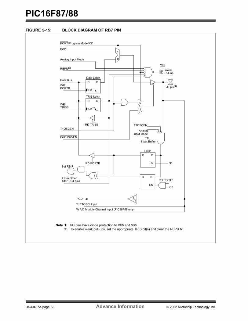
PIC16F87/88
FIGURE 5-15: BLOCK DIAGRAM OF RB7 PINData Latch
From Other
RBPU(2)
P
VDD
I/O pin(1)QD
CK
QD
CK
Q D
EN
Q D
EN
Data Bus
WR
T1OSCEN
Set RBIF
TRIS Latch
RD TRISB
RD PORTB
RB7:RB4 pins
WeakPull-up
RD PORTB
Latch
Q3
Q1
PORTB
Note 1: I/O pins have diode protection to VDD and VSS.2: To enable weak pull-ups, set the appropriate TRIS bit(s) and clear the RBPU bit.
PGD
PGD
PORT/Program Mode/ICD
Analog
TTLInput Buffer
Input Mode
To T1OSCI Input
1
0
PGD DRVEN
T1OSCEN
WRTRISB
To A/D Module Channel Input (PIC16F88 only)
1
0Analog Input Mode
DS30487A-page 68 Advance Information 2002 Microchip Technology Inc.

PIC16F87/88
6.0 TIMER0 MODULEThe Timer0 module timer/counter has the followingfeatures:
• 8-bit timer/counter• Readable and writable• 8-bit software programmable prescaler• Internal or external clock select• Interrupt on overflow from FFh to 00h• Edge select for external clock
Additional information on the Timer0 module isavailable in the PICmicro™ Mid-Range MCU FamilyReference Manual (DS33023).
Figure 6-1 is a block diagram of the Timer0 module andthe prescaler shared with the WDT.
6.1 Timer0 OperationTimer0 operation is controlled through the OPTIONregister (see Register 2-2). Timer mode is selected byclearing bit T0CS (OPTION<5>). In Timer mode, theTimer0 module will increment every instruction cycle(without prescaler). If the TMR0 register is written, the
increment is inhibited for the following two instructioncycles. The user can work around this by writing anadjusted value to the TMR0 register.
Counter mode is selected by setting bit T0CS(OPTION<5>). In Counter mode, Timer0 will increment,either on every rising or falling edge of pin RA4/T0CKI.The incrementing edge is determined by the Timer0Source Edge Select bit T0SE (OPTION<4>). Clearing bitT0SE selects the rising edge. Restrictions on the externalclock input are discussed in detail in Section 6.3.
The prescaler is mutually, exclusively shared betweenthe Timer0 module and the Watchdog Timer. The pres-caler is not readable or writable. Section 6.4 details theoperation of the prescaler.
6.2 Timer0 InterruptThe TMR0 interrupt is generated when the TMR0 reg-ister overflows from FFh to 00h. This overflow sets bitTMR0IF (INTCON<2>). The interrupt can be maskedby clearing bit TMR0IE (INTCON<5>). Bit TMR0IFmust be cleared in software by the Timer0 moduleInterrupt Service Routine before re-enabling this inter-rupt. The TMR0 interrupt cannot awaken the processorfrom SLEEP, since the timer is shut-off during SLEEP.
FIGURE 6-1: BLOCK DIAGRAM OF THE TIMER0/WDT PRESCALER
RA4/T0CKI
T0SE
pin
MUX
CLKO (= FOSC/4)
Sync2
CyclesTMR0 reg
8-bit Prescaler
8 - to - 1 MUX
MUX
M U X
PSA
0 1
0
1
WDTTime-out
PS2:PS0
8
Note: T0CS, T0SE, PSA, PS2:PS0 are (OPTION<5:0>).
PSA
MUX
0
1 0
1
Data Bus
Set Flag bit TMR0IFon Overflow
8
PSAT0CS
Prescaler
31.25 kHz
WDT Timer
WDT Enable bit
16-bitPrescaler
2002 Microchip Technology Inc. Advance Information DS30487A-page 69

PIC16F87/88
6.3 Using Timer0 with an ExternalClockWhen no prescaler is used, the external clock input isthe same as the prescaler output. The synchronizationof T0CKI, with the internal phase clocks, is accom-plished by sampling the prescaler output on the Q2 andQ4 cycles of the internal phase clocks. Therefore, it isnecessary for T0CKI to be high for at least 2 TOSC (anda small RC delay of 20 ns) and low for at least 2 TOSC(and a small RC delay of 20 ns). Refer to the electricalspecification of the desired device.
6.4 PrescalerThere is only one prescaler available, which is mutuallyexclusively shared between the Timer0 module and theWatchdog Timer. A prescaler assignment for theTimer0 module means that the prescaler cannot beused by the Watchdog Timer, and vice-versa. Thisprescaler is not readable or writable (see Figure 6-1).
The PSA and PS2:PS0 bits (OPTION<3:0>) determinethe prescaler assignment and prescale ratio.
When assigned to the Timer0 module, all instructionswriting to the TMR0 register (e.g., CLRF 1, MOVWF 1,BSF 1,x....etc.) will clear the prescaler. When assignedto WDT, a CLRWDT instruction will clear the prescaleralong with the Watchdog Timer. The prescaler is notreadable or writable.
REGISTER 6-1: OPTION_REG REGISTER
Note: Although the prescaler can be assigned toeither the WDT or Timer0, but not both, anew divide counter is implemented in theWDT circuit to give multiple WDT time-outselection. This allows TMR0 and WDT toeach have their own scaler. Refer toSection 15.12 for further details.
Note: Writing to TMR0 when the prescaler isassigned to Timer0, will clear the prescalercount but will not change the prescalerassignment.
R/W-1 R/W-1 R/W-1 R/W-1 R/W-1 R/W-1 R/W-1 R/W-1
RBPU INTEDG T0CS T0SE PSA PS2 PS1 PS0bit 7 bit 0
bit 7 RBPUbit 6 INTEDGbit 5 T0CS: TMR0 Clock Source Select bit
1 = Transition on T0CKI pin 0 = Internal instruction cycle clock (CLKO)
bit 4 T0SE: TMR0 Source Edge Select bit 1 = Increment on high-to-low transition on T0CKI pin 0 = Increment on low-to-high transition on T0CKI pin
bit 3 PSA: Prescaler Assignment bit 1 = Prescaler is assigned to the WDT 0 = Prescaler is assigned to the Timer0 module
bit 2-0 PS<2:0>: Prescaler Rate Select bits
Legend:R = Readable bit W = Writable bit U = Unimplemented bit, read as ‘0’- n = Value at POR ‘1’ = Bit is set ‘0’ = Bit is cleared x = Bit is unknown
Note: To avoid an unintended device RESET, the instruction sequence shown in thePICmicro™ Mid-Range MCU Family Reference Manual (DS33023) must be exe-cuted when changing the prescaler assignment from Timer0 to the WDT. Thissequence must be followed even if the WDT is disabled.
000001010011100101110111
1 : 21 : 41 : 81 : 161 : 321 : 641 : 1281 : 256
1 : 11 : 21 : 41 : 81 : 161 : 321 : 641 : 128
Bit Value TMR0 Rate WDT Rate
DS30487A-page 70 Advance Information 2002 Microchip Technology Inc.

PIC16F87/88
EXAMPLE 6-1: CHANGING THE PRESCALER ASSIGNMENT FROM WDT TO TIMER0TABLE 6-1: REGISTERS ASSOCIATED WITH TIMER0
CLRWDT ; Clear WDT and prescalerBANKSEL OPTION ; Select Bank of OPTIONMOVLW b'xxxx0xxx' ; Select TMR0, new prescaleMOVWF OPTION ; value and clock source
Address Name Bit 7 Bit 6 Bit 5 Bit 4 Bit 3 Bit 2 Bit 1 Bit 0 Value on POR, BOR
Value on all other RESETS
01h,101h TMR0 Timer0 Module Register xxxx xxxx uuuu uuuu0Bh,8Bh,10Bh,18Bh
INTCON GIE PEIE TMR0IE INTE RBIE TMR0IF INTF RBIF 0000 000x 0000 000u
81h,181h OPTION RBPU INTEDG T0CS T0SE PSA PS2 PS1 PS0 1111 1111 1111 1111Legend: x = unknown, u = unchanged, - = unimplemented locations read as ‘0’. Shaded cells are not used by Timer0.
2002 Microchip Technology Inc. Advance Information DS30487A-page 71

PIC16F87/88
NOTES:DS30487A-page 72 Advance Information 2002 Microchip Technology Inc.

PIC16F87/88
7.0 TIMER1 MODULEThe Timer1 module is a 16-bit timer/counter consistingof two 8-bit registers (TMR1H and TMR1L), which arereadable and writable. The TMR1 register pair(TMR1H:TMR1L) increments from 0000h to FFFFhand rolls over to 0000h. The TMR1 interrupt, if enabled,is generated on overflow, which is latched in interruptflag bit TMR1IF (PIR1<0>). This interrupt can beenabled/disabled by setting/clearing TMR1 interruptenable bit TMR1IE (PIE1<0>).
The Timer1 oscillator can be used as a secondary clocksource in Low Power modes. When the T1RUN bit isset, the Timer1 oscillator is providing the system clock.If the Fail-Safe Clock Monitor is enabled, and theTimer1 oscillator fails while providing the system clock,polling the T1RUN bit will indicate whether the clock isbeing provided by the Timer1 oscillator or anothersource.
Timer1 can also be used to provide Real-Time Clock(RTC) functionality to applications with only a minimaladdition of external components or code overhead.
7.1 Timer1 OperationTimer1 can operate in one of three modes:
• as a Timer• as a Synchronous Counter• as an Asynchronous Counter
The Operating mode is determined by the clock selectbit, TMR1CS (T1CON<1>).
In Timer mode, Timer1 increments every instructioncycle. In Counter mode, it increments on every risingedge of the external clock input.
Timer1 can be enabled/disabled by setting/clearingcontrol bit TMR1ON (T1CON<0>).
Timer1 also has an internal “RESET input”. ThisRESET can be generated by the CCP1 module as thespecial event trigger (see Section 9.1). Register 7-1shows the Timer1 Control register.
When the Timer1 oscillator is enabled (T1OSCEN isset), the RB6/T1OSO/T1CKI/PGC and RB7/T1OSI/PGD pins become inputs. That is, the TRISB<7:6>value is ignored and these pins read as ‘0’.
Additional information on timer modules is available inthe PICmicro™ Mid-Range MCU Family ReferenceManual (DS33023).
2002 Microchip Technology Inc. Advance Information DS30487A-page 73

PIC16F87/88
REGISTER 7-1: T1CON: TIMER1 CONTROL REGISTER (ADDRESS 10h)U-0 R-0 R/W-0 R/W-0 R/W-0 R/W-0 R/W-0 R/W-0
— T1RUN T1CKPS1 T1CKPS0 T1OSCEN T1SYNC TMR1CS TMR1ONbit 7 bit 0
bit 7 Unimplemented: Read as ‘0’bit 6 T1RUN: Timer1 System Clock Status bit
1 = System clock is derived from Timer1 oscillator0 = System clock is derived from another source
bit 5-4 T1CKPS<1:0>: Timer1 Input Clock Prescale Select bits11 =1:8 Prescale value10 =1:4 Prescale value01 =1:2 Prescale value00 =1:1 Prescale value
bit 3 T1OSCEN: Timer1 Oscillator Enable Control bit1 = Oscillator is enabled0 = Oscillator is shut-off (the oscillator inverter is turned off to eliminate power drain)
bit 2 T1SYNC: Timer1 External Clock Input Synchronization Control bitTMR1CS = 1:1 = Do not synchronize external clock input0 = Synchronize external clock inputTMR1CS = 0:This bit is ignored. Timer1 uses the internal clock when TMR1CS = 0
bit 1 TMR1CS: Timer1 Clock Source Select bit1 = External clock from pin RB6/T1OSO/T1CKI/PGC (on the rising edge)0 = Internal clock (FOSC/4)
bit 0 TMR1ON: Timer1 On bit1 = Enables Timer10 = Stops Timer1
Legend:R = Readable bit W = Writable bit U = Unimplemented bit, read as ‘0’- n = Value at POR ‘1’ = Bit is set ‘0’ = Bit is cleared x = Bit is unknown
DS30487A-page 74 Advance Information 2002 Microchip Technology Inc.

PIC16F87/88
7.2 Timer1 Operation in Timer ModeTimer mode is selected by clearing the TMR1CS(T1CON<1>) bit. In this mode, the input clock to thetimer is FOSC/4. The synchronize control bit T1SYNC(T1CON<2>) has no effect, since the internal clock isalways in sync.7.3 Timer1 Counter OperationTimer1 may operate in Asynchronous or Synchronousmode, depending on the setting of the TMR1CS bit.
When Timer1 is being incremented via an externalsource, increments occur on a rising edge. After Timer1is enabled in Counter mode, the module must first havea falling edge before the counter begins to increment.
7.4 Timer1 Operation in Synchronized Counter Mode
Counter mode is selected by setting bit TMR1CS. Inthis mode, the timer increments on every rising edge ofclock input on pin RB7/T1OSI/PGD, when bitT1OSCEN is set, or on pin RB6/T1OSO/T1CKI/PGC,when bit T1OSCEN is cleared.
If T1SYNC is cleared, then the external clock input issynchronized with internal phase clocks. The synchro-nization is done after the prescaler stage. Theprescaler stage is an asynchronous ripple counter.
In this configuration, during SLEEP mode, Timer1 willnot increment even if the external clock is present,since the synchronization circuit is shut-off. Theprescaler, however, will continue to increment.
FIGURE 7-1: TIMER1 INCREMENTING EDGE
FIGURE 7-2: TIMER1 BLOCK DIAGRAM
T1CKI(Default High)
T1CKI(Default Low)
Note: Arrows indicate counter increments.
TMR1H TMR1L
T1OSCT1SYNC
TMR1CST1CKPS1:T1CKPS0
Q Clock
T1OSCENEnableOscillator(1)
FOSC/4InternalClock
TMR1ONOn/Off
Prescaler1, 2, 4, 8
Synchronize
det
1
0
0
1
SynchronizedClock Input
2T1OSI
T1OSO/T1CKI
Note 1: When the T1OSCEN bit is cleared, the inverter is turned off. This eliminates power drain.
Set Flag bitTMR1IF onOverflow
TMR1
2002 Microchip Technology Inc. Advance Information DS30487A-page 75

PIC16F87/88
7.5 Timer1 Operation inAsynchronous Counter ModeIf control bit T1SYNC (T1CON<2>) is set, the externalclock input is not synchronized. The timer continues toincrement asynchronous to the internal phase clocks.The timer will continue to run during SLEEP and cangenerate an interrupt on overflow that will wake-up theprocessor. However, special precautions in softwareare needed to read/write the timer (Section 7.5.1).
In Asynchronous Counter mode, Timer1 cannot beused as a time-base for capture or compareoperations.
7.5.1 READING AND WRITING TIMER1 IN ASYNCHRONOUS COUNTER MODE
Reading TMR1H or TMR1L while the timer is runningfrom an external asynchronous clock will ensure a validread (taken care of in hardware). However, the usershould keep in mind that reading the 16-bit timer in two8-bit values itself, poses certain problems, since thetimer may overflow between the reads.
For writes, it is recommended that the user simply stopthe timer and write the desired values. A write conten-tion may occur by writing to the timer registers while theregister is incrementing. This may produce anunpredictable value in the timer register.
Reading the 16-bit value requires some care. Theexample codes provided in Example 7-1 andExample 7-2 demonstrate how to write to and readTimer1 while it is running in Asynchronous mode.
EXAMPLE 7-1: WRITING A 16-BIT FREE-RUNNING TIMER
EXAMPLE 7-2: READING A 16-BIT FREE-RUNNING TIMER
; All interrupts are disabledCLRF TMR1L ; Clear Low byte, Ensures no rollover into TMR1HMOVLW HI_BYTE ; Value to load into TMR1HMOVWF TMR1H, F ; Write High byteMOVLW LO_BYTE ; Value to load into TMR1LMOVWF TMR1H, F ; Write Low byte; Re-enable the Interrupt (if required)CONTINUE ; Continue with your code
; All interrupts are disabledMOVF TMR1H, W ; Read high byteMOVWF TMPHMOVF TMR1L, W ; Read low byteMOVWF TMPLMOVF TMR1H, W ; Read high byteSUBWF TMPH, W ; Sub 1st read with 2nd readBTFSC STATUS,Z ; Is result = 0GOTO CONTINUE ; Good 16-bit read; TMR1L may have rolled over between the read of the high and low bytes.; Reading the high and low bytes now will read a good value.MOVF TMR1H, W ; Read high byteMOVWF TMPHMOVF TMR1L, W ; Read low byteMOVWF TMPL ; Re-enable the Interrupt (if required)CONTINUE ; Continue with your code
DS30487A-page 76 Advance Information 2002 Microchip Technology Inc.

PIC16F87/88
7.6 Timer1 OscillatorA crystal oscillator circuit is built between pins T1OSI(input) and T1OSO (amplifier output). It is enabled bysetting control bit T1OSCEN (T1CON<3>). The oscilla-tor is a low power oscillator rated up to 32.768 kHz. Itwill continue to run during all Power Managed modes.It is primarily intended for a 32 kHz crystal. The circuitfor a typical LP oscillator is shown in Figure 7-3.Table 7-1 shows the capacitor selection for the Timer1oscillator.The user must provide a software time delay to ensureproper oscillator start-up.
FIGURE 7-3: EXTERNAL COMPONENTS FOR THE TIMER1 LP OSCILLATOR
TABLE 7-1: CAPACITOR SELECTION FOR THE TIMER1 OSCILLATOR
7.7 Timer1 Oscillator Layout Considerations
The Timer1 oscillator circuit draws very little power dur-ing operation. Due to the low power nature of the oscil-lator, it may also be sensitive to rapidly changingsignals in close proximity.
The oscillator circuit, shown in Figure 7-3, should belocated as close as possible to the microcontroller.There should be no circuits passing within the oscillatorcircuit boundaries other than VSS or VDD.
If a high speed circuit must be located near the oscilla-tor, a grounded guard ring around the oscillator circuit,as shown in Figure 7-4, may be helpful when used ona single sided PCB, or in addition to a ground plane.
FIGURE 7-4: OSCILLATOR CIRCUIT WITH GROUNDED GUARD RING
7.8 Resetting Timer1 Using a CCP Trigger Output
If the CCP1 module is configured in Compare mode togenerate a “special event trigger" signal(CCP1M3:CCP1M0 = 1011), the signal will resetTimer1 and start an A/D conversion (if the A/D moduleis enabled).
Timer1 must be configured for either Timer or Synchro-nized Counter mode to take advantage of this feature.If Timer1 is running in Asynchronous Counter mode,this RESET operation may not work.
In the event that a write to Timer1 coincides with aspecial event trigger from CCP1, the write will takeprecedence.
In this mode of operation, the CCPR1H:CCPR1L regis-ter pair effectively becomes the period register forTimer1.
Osc Type Freq C1 C2LP 32 kHz 33 pF 33 pF
Note 1: Microchip suggests this value as a startingpoint in validating the oscillator circuit.
2: Higher capacitance increases the stabilityof the oscillator, but also increases thestart-up time.
3: Since each resonator/crystal has its owncharacteristics, the user should consultthe resonator/crystal manufacturer forappropriate values of externalcomponents.
4: Capacitor values are for design guidanceonly.
PIC16F87/88
T1OSI
T1OSOC2
33 pF
C133 pF
XTAL32.768 kHz
Note: See the Notes with Section 7-1 for additionalinformation about capacitor selection.
Note: The special event triggers from the CCP1module will not set interrupt flag bitTMR1IF (PIR1<0>).
OSC1
VSS
OSC2
RB7
RB6
RB5
2002 Microchip Technology Inc. Advance Information DS30487A-page 77

PIC16F87/88
7.9 Resetting Timer1 Register Pair(TMR1H, TMR1L)TMR1H and TMR1L registers are not reset to 00h on aPOR, or any other RESET, except by the CCP1 specialevent triggers.
T1CON register is reset to 00h on a Power-on Reset ora Brown-out Reset, which shuts off the timer andleaves a 1:1 prescale. In all other RESETS, the registeris unaffected.
7.10 Timer1 PrescalerThe prescaler counter is cleared on writes to theTMR1H or TMR1L registers.
7.11 Using Timer1 as a Real-Time Clock
Adding an external LP oscillator to Timer1 (such as theone described in Section 7.6, above), gives users theoption to include RTC functionality to their applications.This is accomplished with an inexpensive watch crystalto provide an accurate time-base, and several lines ofapplication code to calculate the time. When operatingin SLEEP mode and using a battery or super capacitoras a power source, it can completely eliminate the needfor a separate RTC device and battery backup.
The application code routine, RTCisr, shown inExample 7-3, demonstrates a simple method to incre-ment a counter at one-second intervals using an Inter-rupt Service Routine. Incrementing the TMR1 registerpair to overflow triggers the interrupt and calls the rou-tine, which increments the seconds counter by one;additional counters for minutes and hours areincremented as the previous counter overflow.
Since the register pair is 16-bits wide, counting up tooverflow the register directly from a 32.768 kHz clockwould take 2 seconds. To force the overflow at therequired one-second intervals, it is necessary to pre-load it; the simplest method is to set the MSbit ofTMR1H with a BSF instruction. Note that the TMR1Lregister is never pre-loaded or altered; doing so mayintroduce cumulative error over many cycles.
For this method to be accurate, Timer1 must operate inAsynchronous mode, and the Timer1 Overflow Inter-rupt must be enabled (PIE1<0> = 1), as shown in theroutine, RTCinit. The Timer1 oscillator must also beenabled and running at all times.
DS30487A-page 78 Advance Information 2002 Microchip Technology Inc.

PIC16F87/88
EXAMPLE 7-3: IMPLEMENTING A REAL-TIME CLOCK USING A TIMER1 INTERRUPT SERVICETABLE 7-2: REGISTERS ASSOCIATED WITH TIMER1 AS A TIMER/COUNTER
RTCinit banksel TMR1Hmovlw 0x80 ; Preload TMR1 register pairmovwf TMR1H ; for 1 second overflowclrf TMR1Lmovlw b’00001111’ ; Configure for external clock,movwf T1CON ; Asynchronous operation, external oscillatorclrf secs ; Initialize timekeeping registersclrf minsmovlw .12movwf hoursbanksel PIE1bsf PIE1, TMR1IE ; Enable Timer1 interruptreturn
RTCisr banksel TMR1Hbsf TMR1H,7 ; Preload for 1 sec overflowbcf PIR1,TMR1IF ; Clear interrupt flagincf secs,F ; Increment secondsmovf secs,wsublw .60btfss STATUS,Z ; 60 seconds elapsed?return ; No, doneclrf seconds ; Clear secondsincf mins,f ; Increment minutesmovf mins,wsublw .60btfss STATUS,Z ; 60 seconds elapsed?return ; No, doneclrf mins ; Clear minutesincf hours,f ; Increment hoursmovf hours,wsublw .24btfss STATUS,Z ; 24 hours elapsed?return ; No, doneclrf hours ; Clear hoursreturn ; Done
Address Name Bit 7 Bit 6 Bit 5 Bit 4 Bit 3 Bit 2 Bit 1 Bit 0 Value onPOR, BOR
Value on all other RESETS
0Bh, 8Bh,10Bh, 18Bh
INTCON GIE PEIE TMR0IE INTE RBIE TMR0IF INTF RBIF 0000 000x 0000 000u
0Ch PIR1 — ADIF RCIF TXIF SSPIF CCP1IF TMR2IF TMR1IF -000 0000 -000 00008Ch PIE1 — ADIE RCIE TXIE SSPIE CCP1IE TMR2IE TMR1IE -000 0000 -000 00000Eh TMR1L Holding Register for the Least Significant Byte of the 16-bit TMR1 Register xxxx xxxx uuuu uuuu0Fh TMR1H Holding Register for the Most Significant Byte of the 16-bit TMR1 Register xxxx xxxx uuuu uuuu10h T1CON — T1RUN T1CKPS1 T1CKPS0 T1OSCEN T1SYNC TMR1CS TMR1ON -000 0000 -uuu uuuuLegend: x = unknown, u = unchanged, - = unimplemented, read as ‘0’. Shaded cells are not used by the Timer1 module.
2002 Microchip Technology Inc. Advance Information DS30487A-page 79

PIC16F87/88
NOTES:DS30487A-page 80 Advance Information 2002 Microchip Technology Inc.

PIC16F87/88
8.0 TIMER2 MODULETimer2 is an 8-bit timer with a prescaler and apostscaler. It can be used as the PWM time-base forthe PWM mode of the CCP1 module. The TMR2 regis-ter is readable and writable, and is cleared on anydevice RESET.
The input clock (FOSC/4) has a prescale option of 1:1,1:4 or 1:16, selected by control bitsT2CKPS1:T2CKPS0 (T2CON<1:0>).
The Timer2 module has an 8-bit period register, PR2.Timer2 increments from 00h until it matches PR2 andthen resets to 00h on the next increment cycle. PR2 isa readable and writable register. The PR2 register isinitialized to FFh upon RESET.
The match output of TMR2 goes through a 4-bitpostscaler (which gives a 1:1 to 1:16 scaling inclusive)to generate a TMR2 interrupt (latched in flag bitTMR2IF (PIR1<1>)).
Timer2 can be shut-off by clearing control bit TMR2ON(T2CON<2>) to minimize power consumption.
Register 8-1 shows the Timer2 control register.
Additional information on timer modules is available inthe PICmicro™ Mid-Range MCU Family ReferenceManual (DS33023).
8.1 Timer2 Prescaler and PostscalerThe prescaler and postscaler counters are clearedwhen any of the following occurs:
• A write to the TMR2 register• A write to the T2CON register• Any device RESET (Power-on Reset, MCLR,
WDT Reset, or Brown-out Reset)
TMR2 is not cleared when T2CON is written.
8.2 Output of TMR2The output of TMR2 (before the postscaler) is fed to theSynchronous Serial Port module, which optionally usesit to generate a shift clock.
FIGURE 8-1: TIMER2 BLOCK DIAGRAM
Comparator
TMR2Sets Flag
TMR2 reg
Output(1)
RESET
Postscaler
Prescaler
PR2 reg
2
FOSC/4
1:1 1:16
1:1, 1:4, 1:16
EQ
4
bit TMR2IF
Note 1: TMR2 register output can be software selected by the SSP module as a baud clock.
to
2002 Microchip Technology Inc. Advance Information DS30487A-page 81

PIC16F87/88
REGISTER 8-1: T2CON: TIMER2 CONTROL REGISTER (ADDRESS 12h)TABLE 8-1: REGISTERS ASSOCIATED WITH TIMER2 AS A TIMER/COUNTER
U-0 R/W-0 R/W-0 R/W-0 R/W-0 R/W-0 R/W-0 R/W-0— TOUTPS3 TOUTPS2 TOUTPS1 TOUTPS0 TMR2ON T2CKPS1 T2CKPS0
bit 7 bit 0
bit 7 Unimplemented: Read as ‘0’bit 6-3 TOUTPS<3:0>: Timer2 Output Postscale Select bits
0000 = 1:1 Postscale0001 = 1:2 Postscale0010 = 1:3 Postscale•••1111 = 1:16 Postscale
bit 2 TMR2ON: Timer2 On bit1 = Timer2 is on0 = Timer2 is off
bit 1-0 T2CKPS<1:0>: Timer2 Clock Prescale Select bits00 = Prescaler is 101 = Prescaler is 41x = Prescaler is 16
Legend:R = Readable bit W = Writable bit U = Unimplemented bit, read as ‘0’- n = Value at POR ‘1’ = Bit is set ‘0’ = Bit is cleared x = Bit is unknown
Address Name Bit 7 Bit 6 Bit 5 Bit 4 Bit 3 Bit 2 Bit 1 Bit 0 Value onPOR, BOR
Value on all other RESETS
0Bh, 8Bh,10Bh, 18Bh
INTCON GIE PEIE TMR0IE INTE RBIE TMR0IF INTF RBIF 0000 000x 0000 000u
0Ch PIR1 — ADIF RCIF TXIF SSPIF CCP1IF TMR2IF TMR1IF -000 0000 -000 00008Ch PIE1 — ADIE RCIE TXIE SSPIE CCP1IE TMR2IE TMR1IE -000 0000 -000 000011h TMR2 Timer2 Module Register 0000 0000 0000 000012h T2CON — TOUTPS3 TOUTPS2 TOUTPS1 TOUTPS0 TMR2ON T2CKPS1 T2CKPS0 -000 0000 -000 000092h PR2 Timer2 Period Register 1111 1111 1111 1111Legend: x = unknown, u = unchanged, - = unimplemented, read as ‘0’. Shaded cells are not used by the Timer2 module.
DS30487A-page 82 Advance Information 2002 Microchip Technology Inc.

PIC16F87/88
9.0 CAPTURE/COMPARE/PWM (CCP) MODULE
The Capture/Compare/PWM (CCP) module contains a16-bit register that can operate as a:
• 16-bit capture register• 16-bit compare register • PWM master/slave duty cycle register.
Table 9-1 shows the timer resources of the CCPmodule modes.
Capture/Compare/PWM Register1 (CCPR1) is com-prised of two 8-bit registers: CCPR1L (low byte) andCCPR1H (high byte). The CCP1CON register controlsthe operation of CCP1. The special event trigger isgenerated by a compare match which will reset Timer1and start an A/D conversion (if the A/D module isenabled).
The CCP module’s input/output pin (CCP1) can beconfigured as RB0 or RB3. This selection is set in bit 12(CCPMX) of the configuration word.
Additional information on the CCP module is availablein the PICmicro™ Mid-Range MCU Reference Manual,(DS33023) and in Application Note AN594, “Using theCCP Modules” (DS00594).
TABLE 9-1: CCP MODE - TIMER RESOURCE
REGISTER 9-1: CCP1CON: CAPTURE/COMPARE/PWM CONTROL REGISTER 1 (ADDRESS 17h)
CCP Mode Timer Resource
CaptureCompare
PWM
Timer1Timer1Timer2
U-0 U-0 R/W-0 R/W-0 R/W-0 R/W-0 R/W-0 R/W-0— — CCP1X CCP1Y CCP1M3 CCP1M2 CCP1M1 CCP1M0
bit 7 bit 0
bit 7-6 Unimplemented: Read as '0'bit 5-4 CCP1X:CCP1Y: PWM Least Significant bits
Capture mode:UnusedCompare mode:UnusedPWM mode:These bits are the two LSbs of the PWM duty cycle. The eight MSbs are found in CCPRxL.
bit 3-0 CCP1M<3:0>: CCP1 Mode Select bits0000 = Capture/Compare/PWM disabled (resets CCP1 module)0100 = Capture mode, every falling edge0101 = Capture mode, every rising edge0110 = Capture mode, every 4th rising edge0111 = Capture mode, every 16th rising edge1000 = Compare mode, set output on match (CCP1IF bit is set)1001 = Compare mode, clear output on match (CCP1IF bit is set)1010 = Compare mode, generate software interrupt on match (CCP1IF bit is set,
CCP1 pin is unaffected)1011 = Compare mode, trigger special event (CCP1IF bit is set, CCP1 pin is unaffected);
CCP1 resets TMR1 and starts an A/D conversion (if A/D module is enabled)11xx = PWM mode
Legend:R = Readable bit W = Writable bit U = Unimplemented bit, read as ‘0’- n = Value at POR ‘1’ = Bit is set ‘0’ = Bit is cleared x = Bit is unknown
2002 Microchip Technology Inc. Advance Information DS30487A-page 83

PIC16F87/88
9.1 Capture ModeIn Capture mode, CCPR1H:CCPR1L captures the16-bit value of the TMR1 register when an event occurson CCP1 pin. An event is defined as:• Every falling edge• Every rising edge• Every 4th rising edge• Every 16th rising edge
An event is selected by control bits CCP1M3:CCP1M0(CCP1CON<3:0>). When a capture is made, the inter-rupt request flag bit CCP1IF (PIR1<2>) is set. It mustbe cleared in software. If another capture occurs beforethe value in register CCPR1 is read, the old capturedvalue is overwritten by the new captured value.
9.1.1 CCP PIN CONFIGURATION
In Capture mode, the CCP1 pin should be configuredas an input by setting the TRISB<x> bit.
FIGURE 9-1: CAPTURE MODE OPERATION BLOCK DIAGRAM
9.1.2 TIMER1 MODE SELECTION
Timer1 must be running in Timer mode or Synchro-nized Counter mode for the CCP module to use thecapture feature. In Asynchronous Counter mode, thecapture operation may not work.
9.1.3 SOFTWARE INTERRUPT
When the Capture mode is changed, a false captureinterrupt may be generated. The user should keep bitCCP1IE (PIE1<2>) clear to avoid false interrupts andshould clear the flag bit CCP1IF, following any suchchange in Operating mode.
9.1.4 CCP PRESCALER
There are four prescaler settings, specified by bitsCCP1M3:CCP1M0. Whenever the CCP module isturned off, or the CCP module is not in Capture mode,the prescaler counter is cleared. This means that anyRESET will clear the prescaler counter.
Switching from one capture prescaler to another maygenerate an interrupt. Also, the prescaler counter willnot be cleared, therefore, the first capture may be froma non-zero prescaler. Example 9-1 shows the recom-mended method for switching between capture pres-calers. This example also clears the prescaler counterand will not generate the “false” interrupt.
EXAMPLE 9-1: CHANGING BETWEEN CAPTURE PRESCALERS
Note 1: If the CCP1 pin is configured as anoutput, a write to the port can cause acapture condition.
2: The TRISB bit (0 or 3) is dependent uponthe setting of configuration bit 12(CCPMX).
CCPR1H CCPR1L
TMR1H TMR1L
Set Flag bit CCP1IF(PIR1<2>)
CaptureEnable
Q’sCCP1CON<3:0>
CCP1 Pin
Prescaler÷ 1, 4, 16
andEdge Detect
CLRF CCP1CON ;Turn CCP module offMOVLW NEW_CAPT_PS ;Load the W reg with
;the new prescaler;move value and CCP ON
MOVWF CCP1CON ;Load CCP1CON with this;value
DS30487A-page 84 Advance Information 2002 Microchip Technology Inc.

PIC16F87/88
9.2 Compare ModeIn Compare mode, the 16-bit CCPR1 register value isconstantly compared against the TMR1 register pairvalue. When a match occurs, the CCP1 pin is:• Driven High• Driven Low• Remains Unchanged
The action on the pin is based on the value of controlbits CCP1M3:CCP1M0 (CCP1CON<3:0>). At thesame time, interrupt flag bit CCP1IF is set.
FIGURE 9-2: COMPARE MODE OPERATION BLOCK DIAGRAM
9.2.1 CCP PIN CONFIGURATION
The user must configure the CCP1 pin as an output byclearing the TRISB<x> bit.
9.2.2 TIMER1 MODE SELECTION
Timer1 must be running in Timer mode or Synchro-nized Counter mode if the CCP module is using thecompare feature. In Asynchronous Counter mode, thecompare operation may not work.
9.2.3 SOFTWARE INTERRUPT MODE
When generate software interrupt is chosen, the CCP1pin is not affected. Only a CCP interrupt is generated (ifenabled).
9.2.4 SPECIAL EVENT TRIGGER
In this mode, an internal hardware trigger is generatedthat may be used to initiate an action.
The special event trigger output of CCP1 resets theTMR1 register pair and starts an A/D conversion (if theA/D module is enabled). This allows the CCPR1 regis-ter to effectively be a 16-bit programmable periodregister for Timer1.
TABLE 9-2: REGISTERS ASSOCIATED WITH CAPTURE, COMPARE AND TIMER1
CCPR1H CCPR1L
TMR1H TMR1L
ComparatorQ S
R
OutputLogic
Special Event Trigger
Set Flag bit CCP1IF(PIR1<2>)
MatchCCP1 pin
TRISB<x>CCP1CON<3:0>Mode Select
Output Enable
Special event trigger will:• RESET Timer1, but not set interrupt flag bit TMR1IF
(PIR1<0>)• Set bit GO/DONE (ADCON0<2>) bit, which starts an A/D
conversion
Note 1: Clearing the CCP1CON register will forcethe CCP1 compare output latch to thedefault low level. This is not the datalatch.
2: The TRISB bit (0 or 3) is dependent uponthe setting of configuration bit 12(CCPMX).
Note: The special event trigger from the CCP1module will not set interrupt flag bitTMR1IF (PIR1<0>).
Address Name Bit 7 Bit 6 Bit 5 Bit 4 Bit 3 Bit 2 Bit 1 Bit 0 Value onPOR, BOR
Value onall otherRESETS
0Bh,8Bh10BH,18Bh
INTCON GIE PEIE TMR0IE INTE RBIE TMR0IF INTF RBIF 0000 000x 0000 000u
0Ch PIR1 — ADIF RCIF TXIF SSPIF CCP1IF TMR2IF TMR1IF -000 0000 -000 00008Ch PIE1 — ADIE RCIE TXIE SSPIE CCP1IE TMR2IE TMR1IE -000 0000 -000 000086h TRISB PORTB Data Direction Register 1111 1111 1111 11110Eh TMR1L Holding Register for the Least Significant Byte of the 16-bit TMR1 Register xxxx xxxx uuuu uuuu0Fh TMR1H Holding Register for the Most Significant Byte of the 16-bit TMR1 Register xxxx xxxx uuuu uuuu10h T1CON — T1RUN T1CKPS1 T1CKPS0 T1OSCEN T1SYNC TMR1CS TMR1ON -000 0000 -uuu uuuu15h CCPR1L Capture/Compare/PWM Register1 (LSB) xxxx xxxx uuuu uuuu16h CCPR1H Capture/Compare/PWM Register1 (MSB) xxxx xxxx uuuu uuuu17h CCP1CON — — CCP1X CCP1Y CCP1M3 CCP1M2 CCP1M1 CCP1M0 --00 0000 --00 0000Legend: x = unknown, u = unchanged, - = unimplemented, read as ‘0’. Shaded cells are not used by Capture and Timer1.
2002 Microchip Technology Inc. Advance Information DS30487A-page 85

PIC16F87/88
9.3 PWM ModeIn Pulse Width Modulation (PWM) mode, the CCP1 pinproduces up to a 10-bit resolution PWM output. Sincethe CCP1 pin is multiplexed with the PORTB data latch,the TRISB<x> bit must be cleared to make the CCP1pin an output.Figure 9-3 shows a simplified block diagram of theCCP module in PWM mode.
For a step by step procedure on how to setup the CCPmodule for PWM operation, see Section 9.3.3.
FIGURE 9-3: SIMPLIFIED PWM BLOCK DIAGRAM
A PWM output (Figure 9-4) has a time-base (period)and a time that the output stays high (duty cycle). Thefrequency of the PWM is the inverse of the period(1/period).
FIGURE 9-4: PWM OUTPUT
9.3.1 PWM PERIOD
The PWM period is specified by writing to the PR2register. The PWM period can be calculated using thefollowing formula.
EQUATION 9-1:
PWM frequency is defined as 1 / [PWM period].
When TMR2 is equal to PR2, the following three eventsoccur on the next increment cycle:
• TMR2 is cleared• The CCP1 pin is set (exception: if PWM duty
cycle = 0%, the CCP1 pin will not be set)• The PWM duty cycle is latched from CCPR1L into
CCPR1H
9.3.2 PWM DUTY CYCLE
The PWM duty cycle is specified by writing to theCCPR1L register and to the CCP1CON<5:4> bits. Upto 10-bit resolution is available. The CCPR1L containsthe eight MSbs and the CCP1CON<5:4> contains thetwo LSbs. This 10-bit value is represented byCCPR1L:CCP1CON<5:4>. The following equation isused to calculate the PWM duty cycle in time.
EQUATION 9-2:
CCPR1L and CCP1CON<5:4> can be written to at anytime, but the duty cycle value is not latched intoCCPR1H until after a match between PR2 and TMR2occurs (i.e., the period is complete). In PWM mode,CCPR1H is a read only register.
The CCPR1H register and a 2-bit internal latch areused to double buffer the PWM duty cycle. This doublebuffering is essential for glitchless PWM operation.
When the CCPR1H and 2-bit latch match TMR2, con-catenated with an internal 2-bit Q clock or 2 bits of theTMR2 prescaler, the CCP1 pin is cleared.
Note: Clearing the CCP1CON register will forcethe CCP1 PWM output latch to the defaultlow level. This is not the PORTB I/O datalatch.
CCPR1L
CCPR1H (Slave)
Comparator
TMR2
Comparator
PR2
(Note 1)
R Q
S
Duty Cycle RegistersCCP1CON<5:4>
Clear Timer,CCP1 pin and latch D.C.
TRISB<x>
CCP1 pin
Note 1: 8-bit timer is concatenated with 2-bit internal Q clockor 2 bits of the prescaler to create 10-bit time-base.
Period
Duty Cycle
TMR2 = PR2
TMR2 = Duty Cycle
TMR2 = PR2
Note: The Timer2 postscaler (see Section 8.0) isnot used in the determination of the PWMfrequency. The postscaler could be usedto have a servo update rate at a differentfrequency than the PWM output.
PWM period = [(PR2) + 1] • 4 • TOSC •(TMR2 prescale value)
PWM duty cycle = (CCPR1L:CCP1CON<5:4>) •TOSC • (TMR2 prescale value)
DS30487A-page 86 Advance Information 2002 Microchip Technology Inc.

PIC16F87/88
The maximum PWM resolution (bits) for a given PWMfrequency is given by the following formula.EQUATION 9-3:
9.3.3 SETUP FOR PWM OPERATION
The following steps should be taken when configuringthe CCP module for PWM operation:
1. Set the PWM period by writing to the PR2 register.2. Set the PWM duty cycle by writing to the
CCPR1L register and CCP1CON<5:4> bits.3. Make the CCP1 pin an output by clearing the
TRISB<x> bit.4. Set the TMR2 prescale value and enable Timer2
by writing to T2CON.5. Configure the CCP1 module for PWM operation.
TABLE 9-3: EXAMPLE PWM FREQUENCIES AND RESOLUTIONS AT 20 MHz
TABLE 9-4: REGISTERS ASSOCIATED WITH PWM AND TIMER2
Note: If the PWM duty cycle value is longer thanthe PWM period, the CCP1 pin will not becleared.
log(FPWM
log(2)
FOSC )bits=Resolution
Note: The TRISB bit (0 or 3) is dependant uponthe setting of configuration bit 12(CCPMX).
PWM Frequency 1.22 kHz 4.88 kHz 19.53 kHz 78.12 kHz 156.3 kHz 208.3 kHz
Timer Prescaler (1, 4, 16) 16 4 1 1 1 1PR2 Value 0xFF 0xFF 0xFF 0x3F 0x1F 0x17Maximum Resolution (bits) 10 10 10 8 7 5.5
Address Name Bit 7 Bit 6 Bit 5 Bit 4 Bit 3 Bit 2 Bit 1 Bit 0 Value onPOR, BOR
Value on all otherRESETS
0Bh,8Bh10Bh,18Bh
INTCON GIE PEIE TMR0IE INTE RBIE TMR0IF INTF RBIF 0000 000x 0000 000u
0Ch PIR1 — ADIF RCIF TXIF SSPIF CCP1IF TMR2IF TMR1IF -000 0000 -000 00008Ch PIE1 — ADIE RCIE TXIE SSPIE CCP1IE TMR2IE TMR1IE -000 0000 -000 000086h TRISB PORTB Data Direction Register 1111 1111 1111 111111h TMR2 Timer2 Module Register 0000 0000 0000 000092h PR2 Timer2 Module Period Register 1111 1111 1111 111112h T2CON — TOUTPS3 TOUTPS2 TOUTPS1 TOUTPS0 TMR2ON T2CKPS1 T2CKPS0 -000 0000 -000 000015h CCPR1L Capture/Compare/PWM Register1 (LSB) xxxx xxxx uuuu uuuu16h CCPR1H Capture/Compare/PWM Register1 (MSB) xxxx xxxx uuuu uuuu17h CCP1CON — — CCP1X CCP1Y CCP1M3 CCP1M2 CCP1M1 CCP1M0 --00 0000 --00 0000Legend: x = unknown, u = unchanged, - = unimplemented, read as ‘0’. Shaded cells are not used by PWM and Timer2.
2002 Microchip Technology Inc. Advance Information DS30487A-page 87

PIC16F87/88
NOTES:DS30487A-page 88 Advance Information 2002 Microchip Technology Inc.

PIC16F87/88
10.0 SYNCHRONOUS SERIAL PORT (SSP) MODULE
10.1 SSP Module OverviewThe Synchronous Serial Port (SSP) module is a serialinterface useful for communicating with other periph-eral or microcontroller devices. These peripheraldevices may be Serial EEPROMs, shift registers, dis-play drivers, A/D converters, etc. The SSP module canoperate in one of two modes:
• Serial Peripheral Interface (SPI)• Inter-Integrated Circuit (I2C)
An overview of I2C operations and additional informa-tion on the SSP module can be found in the PICmicro™Mid-Range MCU Family Reference Manual(DS33023).
Refer to Application Note AN578, “Use of the SSPModule in the I 2C Multi-Master Environment”(DS00578).
10.2 SPI ModeThis section contains register definitions andoperational characteristics of the SPI module.
SPI mode allows 8 bits of data to be synchronouslytransmitted and received simultaneously. Toaccomplish communication, typically three pins areused:
• Serial Data Out (SDO) RB2/SDO/RX/DT• Serial Data In (SDI) RB1/SDI/SDA• Serial Clock (SCK) RB4/SCK/SCL
Additionally, a fourth pin may be used when in a Slavemode of operation:
• Slave Select (SS) RB5/SS/TX/CK
When initializing the SPI, several options need to bespecified. This is done by programming the appropriatecontrol bits in the SSPCON register (SSPCON<5:0>)and the SSPSTAT register (SSPSTAT<7:6>). Thesecontrol bits allow the following to be specified:
• Master mode (SCK is the clock output)• Slave mode (SCK is the clock input)• Clock Polarity (IDLE state of SCK)• Clock Edge (output data on rising/falling
edge of SCK)• Clock Rate (Master mode only)• Slave Select mode (Slave mode only)
2002 Microchip Technology Inc. Advance Information DS30487A-page 89

PIC16F87/88
REGISTER 10-1: SSPSTAT: SYNCHRONOUS SERIAL PORT STATUS REGISTER (ADDRESS 94h)R/W-0 R/W-0 R-0 R-0 R-0 R-0 R-0 R-0
SMP CKE D/A P S R/W UA BFbit 7 bit 0
bit 7 SMP: SPI Data Input Sample Phase bitSPI Master mode:1 = Input data sampled at end of data output time0 = Input data sampled at middle of data output time (Microwire®)SPI Slave mode:This bit must be cleared when SPI is used in Slave modeI2 C mode:This bit must be maintained clear
bit 6 CKE: SPI Clock Edge Select bitSPI mode, CKP = 0:1 = Data transmitted on rising edge of SCK (Microwire alternate)0 = Data transmitted on falling edge of SCKSPI mode, CKP = 1:1 = Data transmitted on falling edge of SCK (Microwire alternate)0 = Data transmitted on rising edge of SCKI2 C mode:This bit must be maintained clear
bit 5 D/A: Data/Address bit (I2C mode only)In I2 C Slave mode:1 = Indicates that the last byte received was data0 = Indicates that the last byte received was address
bit 4 P: STOP bit(1) (I2C mode only)1 = Indicates that a STOP bit has been detected last0 = STOP bit was not detected last
bit 3 S: START bit(1) (I2C mode only)1 = Indicates that a START bit has been detected last (this bit is ‘0’ on RESET)0 = START bit was not detected last
bit 2 R/W: Read/Write Information bit (I2C mode only)Holds the R/W bit information following the last address match, and is only valid from address matchto the next START bit, STOP bit, or ACK bit1 = Read0 = Write
bit 1 UA: Update Address bit (10-bit I2C mode only)1 = Indicates that the user needs to update the address in the SSPADD register0 = Address does not need to be updated
bit 0 BF: Buffer Full Status bitReceive (SPI and I2 C modes):1 = Receive complete, SSPBUF is full0 = Receive not complete, SSPBUF is emptyTransmit (In I2 C mode only):1 = Transmit in progress, SSPBUF is full (8 bits)0 = Transmit complete, SSPBUF is empty
Note 1: This bit is cleared when the SSP module is disabled (i.e., the SSPEN bit is cleared).
Legend:R = Readable bit W = Writable bit U = Unimplemented bit, read as ‘0’- n = Value at POR ‘1’ = Bit is set ‘0’ = Bit is cleared x = Bit is unknown
DS30487A-page 90 Advance Information 2002 Microchip Technology Inc.

PIC16F87/88
REGISTER 10-2: SSPCON: SYNCHRONOUS SERIAL PORT CONTROL REGISTER 1(ADDRESS 14h) R/W-0 R/W-0 R/W-0 R/W-0 R/W-0 R/W-0 R/W-0 R/W-0
WCOL SSPOV SSPEN CKP SSPM3 SSPM2 SSPM1 SSPM0bit 7 bit 0
bit 7 WCOL: Write Collision Detect bit1 = An attempt to write the SSPBUF register failed because the SSP module is busy
(must be cleared in software)0 = No collision
bit 6 SSPOV: Receive Overflow Indicator bitIn SPI mode:1 = A new byte is received while the SSPBUF register is still holding the previous data. In case of over-
flow, the data in SSPSR is lost. Overflow can only occur in Slave mode. The user must read theSSPBUF, even if only transmitting data, to avoid setting overflow. In Master mode, the overflow bitis not set since each new reception (and transmission) is initiated by writing to the SSPBUFregister.
0 = No overflowIn I2 C mode:1 = A byte is received while the SSPBUF register is still holding the previous byte. SSPOV is a "don’t
care" in Transmit mode. SSPOV must be cleared in software in either mode.0 = No overflow
bit 5 SSPEN: Synchronous Serial Port Enable bit(1) In SPI mode:1 = Enables serial port and configures SCK, SDO, and SDI as serial port pins0 = Disables serial port and configures these pins as I/O port pinsIn I2 C mode:1 = Enables the serial port and configures the SDA and SCL pins as serial port pins0 = Disables serial port and configures these pins as I/O port pins
bit 4 CKP: Clock Polarity Select bitIn SPI mode:1 = Transmit happens on falling edge, receive on rising edge. IDLE state for clock is a high level.0 = Transmit happens on rising edge, receive on falling edge. IDLE state for clock is a low level.In I2 C Slave mode:SCK release control1 = Enable clock0 = Holds clock low (clock stretch). (Used to ensure data setup time.)
bit 3-0 SSPM<3:0>: Synchronous Serial Port Mode Select bits0000 = SPI Master mode, clock = OSC/40001 = SPI Master mode, clock = OSC/160010 = SPI Master mode, clock = OSC/640011 = SPI Master mode, clock = TMR2 output/20100 = SPI Slave mode, clock = SCK pin. SS pin control enabled.0101 = SPI Slave mode, clock = SCK pin. SS pin control disabled. SS can be used as I/O pin.0110 = I2C Slave mode, 7-bit address0111 = I2C Slave mode, 10-bit address1011 = I2C firmware controlled Master mode (Slave IDLE)1110 = I2C Slave mode, 7-bit address with START and STOP bit interrupts enabled1111 = I2C Slave mode, 10-bit address with START and STOP bit interrupts enabled1000, 1001, 1010, 1100, 1101 = Reserved
Note 1: In both modes, when enabled, these pins must be properly configured as input or output.
Legend:R = Readable bit W = Writable bit U = Unimplemented bit, read as ‘0’- n = Value at POR ‘1’ = Bit is set ‘0’ = Bit is cleared x = Bit is unknown
2002 Microchip Technology Inc. Advance Information DS30487A-page 91

PIC16F87/88
FIGURE 10-1: SSP BLOCK DIAGRAM(SPI MODE) To enable the serial port, SSP enable bit, SSPEN(SSPCON<5>), must be set. To reset or reconfigureSPI mode, clear bit SSPEN, re-initialize the SSPCONregister, and then set bit SSPEN. This configures theSDI, SDO, SCK, and SS pins as serial port pins. For thepins to behave as the serial port function, they musthave their data direction bits (in the TRISB register)appropriately programmed. That is:
• SDI must have TRISB<1> set• SDO must have TRISB<2> cleared• SCK (Master mode) must have TRISB<4> cleared• SCK (Slave mode) must have TRISB<4> set • SS must have TRISB<5> set
TABLE 10-1: REGISTERS ASSOCIATED WITH SPI OPERATION
Read Write
InternalData Bus
RB1/SDI/SDA
RB2/SDO/RX/DT
RB5/SS/
RB4/SCK/
SSPSR reg
SSPBUF reg
SSPM3:SSPM0
bit0 ShiftClock
SS ControlEnable
EdgeSelect
Clock Select
TMR2 Output
TCYPrescaler4, 16, 64
TRISB<4>
2
EdgeSelect
2
4
SCL
TX/CKNote 1: When the SPI is in Slave mode with SS pin
control enabled (SSPCON<3:0> = 0100),the SPI module will reset if the SS pin isset to VDD.
2: If the SPI is used in Slave mode withCKE = 1, then the SS pin control must beenabled.
3: When the SPI is in Slave mode with SS pincontrol enabled (SSPCON<3:0> = 0100),the state of SS pin can affect the stateread back from the TRISB<5> bit. ThePeripheral OE signal from the SSP mod-ule into PORTB controls the state that isread back from the TRISB<5> bit. If Read-Modify-Write instructions, such as BSF,are performed on the TRISB register whilethe SS pin is high, this will cause theTRISB<5> bit to be set, thus disabling theSDO output.
Address Name Bit 7 Bit 6 Bit 5 Bit 4 Bit 3 Bit 2 Bit 1 Bit 0 Value on POR, BOR
Value onall otherRESETS
0Bh,8Bh10Bh,18Bh
INTCON GIE PEIE TMR0IE INTE RBIE TMR0IF INTF RBIF 0000 000x 0000 000u
0Ch PIR1 — ADIF RCIF TXIF SSPIF CCP1IF TMR2IF TMR1IF -000 0000 -000 00008Ch PIE1 — ADIE RCIE TXIE SSPIE CCP1IE TMR2IE TMR1IE -000 0000 -000 000086h TRISB PORTB Data Direction Register 1111 1111 1111 111113h SSPBUF Synchronous Serial Port Receive Buffer/Transmit Register xxxx xxxx uuuu uuuu14h SSPCON WCOL SSPOV SSPEN CKP SSPM3 SSPM2 SSPM1 SSPM0 0000 0000 0000 000094h SSPSTAT SMP CKE D/A P S R/W UA BF 0000 0000 0000 0000Legend: x = unknown, u = unchanged, - = unimplemented, read as ‘0’. Shaded cells are not used by the SSP in SPI mode.
DS30487A-page 92 Advance Information 2002 Microchip Technology Inc.

PIC16F87/88
FIGURE 10-2: SPI MODE TIMING, MASTER MODEFIGURE 10-3: SPI MODE TIMING (SLAVE MODE WITH CKE = 0)
FIGURE 10-4: SPI MODE TIMING (SLAVE MODE WITH CKE = 1)
SCK (CKP = 0,
SDI (SMP = 0)
SSPIF
bit7 bit6 bit5 bit4 bit3 bit2 bit1 bit0
SDI (SMP = 1)
SCK (CKP = 0,
SCK (CKP = 1,
SCK (CKP = 1,
SDO
bit7
bit7 bit0
bit0
CKE = 0)
CKE = 1)
CKE = 0)
CKE = 1)
SCK (CKP = 0)
SDI (SMP = 0)
SSPIF
bit7 bit6 bit5 bit4 bit3 bit2 bit1 bit0
SCK (CKP = 1)
SDO
bit7 bit0
SS (Optional)
SCK (CKP = 0)
SDI (SMP = 0)
SSPIF
bit7 bit6 bit5 bit4 bit3 bit2 bit1 bit0
SCK (CKP = 1)
SDO
bit7 bit0
SS
2002 Microchip Technology Inc. Advance Information DS30487A-page 93

PIC16F87/88
10.3 SSP I2C Mode OperationThe SSP module in I2C mode fully implements all slavefunctions, except general call support, and providesinterrupts on START and STOP bits in hardware tofacilitate firmware implementations of the master func-tions. The SSP module implements the Standard modespecifications, as well as 7-bit and 10-bit addressing.Two pins are used for data transfer. These are theRB4/SCK/SCL pin, which is the clock (SCL), and theRB1/SDI/SDA pin, which is the data (SDA). The usermust configure these pins as inputs or outputs throughthe TRISB<4,1> bits.
The SSP module functions are enabled by setting SSPEnable bit SSPEN (SSPCON<5>).
FIGURE 10-5: SSP BLOCK DIAGRAM (I2C MODE)
The SSP module has five registers for I2C operation:
• SSP Control Register (SSPCON)• SSP Status Register (SSPSTAT)• Serial Receive/Transmit Buffer (SSPBUF)• SSP Shift Register (SSPSR) - Not directly
accessible• SSP Address Register (SSPADD)
The SSPCON register allows control of the I2C opera-tion. Four mode selection bits (SSPCON<3:0>) allowone of the following I2C modes to be selected:
• I2C Slave mode (7-bit address)• I2C Slave mode (10-bit address)• I2C Slave mode (7-bit address), with START and
STOP bit interrupts enabled to support firmware Master mode
• I2C Slave mode (10-bit address), with START and STOP bit interrupts enabled to support firmware Master mode
• I2C Firmware controlled Master operation with START and STOP bit interrupts enabled, Slave is IDLE
Selection of any I2C mode, with the SSPEN bit set,forces the SCL and SDA pins to be open drain, pro-vided these pins are programmed to inputs by settingthe appropriate TRISB bits. Pull-up resistors must beprovided externally to the SCL and SDA pins for properoperation of the I2C module.
Additional information on SSP I2C operation may befound in the PICmicro™ Mid-Range MCU ReferenceManual (DS33023).
10.3.1 SLAVE MODE
In Slave mode, the SCL and SDA pins must be config-ured as inputs (TRISB<4,1> set). The SSP module willoverride the input state with the output data, whenrequired (slave-transmitter).
When an address is matched, or the data transfer afteran address match is received, the hardware automati-cally will generate the Acknowledge (ACK) pulse, andthen load the SSPBUF register with the received valuecurrently in the SSPSR register.
Either or both of the following conditions will cause theSSP module not to give this ACK pulse:
a) The buffer full bit BF (SSPSTAT<0>) was setbefore the transfer was received.
b) The overflow bit SSPOV (SSPCON<6>) was setbefore the transfer was received.
In this case, the SSPSR register value is not loadedinto the SSPBUF, but bit SSPIF (PIR1<3>) is set.Table 10-2 shows what happens when a data transferbyte is received, given the status of bits BF andSSPOV. The shaded cells show the condition whereuser software did not properly clear the overflow condi-tion. Flag bit BF is cleared by reading the SSPBUFregister while bit SSPOV is cleared through software.
The SCL clock input must have a minimum high andlow for proper operation. The high and low times of theI2C specification, as well as the requirement of the SSPmodule, are shown in timing parameter #100 andparameter #101.
Read Write
SSPSR Reg
Match Detect
SSPADD Reg
START and STOP Bit Detect
SSPBUF Reg
InternalData Bus
Addr Match
Set, RESETS, P Bits(SSPSTAT Reg)
RB4/SCK/
RB1/
ShiftClock
MSbSDI/
LSb
SDA
SCL
DS30487A-page 94 Advance Information 2002 Microchip Technology Inc.

PIC16F87/88
10.3.1.1 AddressingOnce the SSP module has been enabled, it waits for aSTART condition to occur. Following the START condi-tion, the eight bits are shifted into the SSPSR register.All incoming bits are sampled with the rising edge of theclock (SCL) line. The value of register SSPSR<7:1> iscompared to the value of the SSPADD register. Theaddress is compared on the falling edge of the eighthclock (SCL) pulse. If the addresses match, and the BFand SSPOV bits are clear, the following events occur:a) The SSPSR register value is loaded into theSSPBUF register.
b) The buffer full bit, BF is set.c) An ACK pulse is generated.d) SSP interrupt flag bit, SSPIF (PIR1<3>), is set
(interrupt is generated if enabled) - on the fallingedge of the ninth SCL pulse.
In 10-bit Address mode, two address bytes need to bereceived by the slave device. The five Most Significantbits (MSbs) of the first address byte specify if this is a10-bit address. Bit R/W (SSPSTAT<2>) must specify awrite so the slave device will receive the secondaddress byte. For a 10-bit address, the first byte wouldequal ‘1111 0 A9 A8 0’, where A9 and A8 are thetwo MSbs of the address.
The sequence of events for 10-bit address is asfollows, with steps 7- 9 for slave-transmitter:
1. Receive first (high) byte of address (bits SSPIF,BF, and bit UA (SSPSTAT<1>) are set).
2. Update the SSPADD register with second (low)byte of address (clears bit UA and releases theSCL line).
3. Read the SSPBUF register (clears bit BF) andclear flag bit SSPIF.
4. Receive second (low) byte of address (bitsSSPIF, BF, and UA are set).
5. Update the SSPADD register with the first (high)byte of Address, if match releases SCL line, thiswill clear bit UA.
6. Read the SSPBUF register (clears bit BF) andclear flag bit SSPIF.
7. Receive Repeated START condition.8. Receive first (high) byte of address (bits SSPIF
and BF are set).9. Read the SSPBUF register (clears bit BF) and
clear flag bit SSPIF.
10.3.1.2 ReceptionWhen the R/W bit of the address byte is clear and anaddress match occurs, the R/W bit of the SSPSTATregister is cleared. The received address is loaded intothe SSPBUF register.
When the address byte overflow condition exists, thena no Acknowledge (ACK) pulse is given. An overflowcondition is indicated if either bit BF (SSPSTAT<0>) isset, or bit SSPOV (SSPCON<6>) is set.
An SSP interrupt is generated for each data transferbyte. Flag bit SSPIF (PIR1<3>) must be cleared in soft-ware. The SSPSTAT register is used to determine thestatus of the byte.
10.3.1.3 TransmissionWhen the R/W bit of the incoming address byte is setand an address match occurs, the R/W bit of theSSPSTAT register is set. The received address isloaded into the SSPBUF register. The ACK pulse willbe sent on the ninth bit, and pin RB4/SCK/SCL is heldlow. The transmit data must be loaded into theSSPBUF register, which also loads the SSPSR regis-ter. Then, pin RB4/SCK/SCL should be enabled by set-ting bit CKP (SSPCON<4>). The master device mustmonitor the SCL pin prior to asserting another clockpulse. The slave devices may be holding off the masterdevice by stretching the clock. The eight data bits areshifted out on the falling edge of the SCL input. Thisensures that the SDA signal is valid during the SCLhigh time (Figure 10-7).
An SSP interrupt is generated for each data transferbyte. Flag bit SSPIF must be cleared in software, andthe SSPSTAT register is used to determine the statusof the byte. Flag bit SSPIF is set on the falling edge ofthe ninth clock pulse.
As a slave-transmitter, the ACK pulse from the master-receiver is latched on the rising edge of the ninth SCLinput pulse. If the SDA line was high (not ACK), thenthe data transfer is complete. When the ACK is latchedby the slave device, the slave logic is reset (resetsSSPSTAT register) and the slave device then monitorsfor another occurrence of the START bit. If the SDA linewas low (ACK), the transmit data must be loaded intothe SSPBUF register, which also loads the SSPSR reg-ister. Then, pin RB4/SCK/SCL should be enabled bysetting bit CKP.
2002 Microchip Technology Inc. Advance Information DS30487A-page 95

PIC16F87/88
TABLE 10-2: DATA TRANSFER RECEIVED BYTE ACTIONSFIGURE 10-6: I2C WAVEFORMS FOR RECEPTION (7-BIT ADDRESS)
FIGURE 10-7: I2C WAVEFORMS FOR TRANSMISSION (7-BIT ADDRESS)
Status Bits as DataTransfer is Received SSPSR → SSPBUF Generate ACK Pulse Set bit SSPIF
(SSP Interrupt Occurs if Enabled)BF SSPOV
0 0 Yes Yes Yes
1 0 No No Yes
1 1 No No Yes
0 1 No No YesNote 1: Shaded cells show the conditions where the user software did not properly clear the overflow condition.
P98765
D0D1D2D3D4D5D6D7
S
A7 A6 A5 A4 A3 A2 A1SDA
SCL 1 2 3 4 5 6 7 8 9 1 2 3 4 5 6 7 8 9 1 2 3 4
Bus Masterterminatestransfer.
Bit SSPOV is set because the SSPBUF register is still full.
Cleared in Software
SSPBUF Register is Read
ACK Receiving DataReceiving DataD0D1D2D3D4D5D6D7ACK
R/W=0Receiving Address
SSPIF (PIR1<3>)
BF (SSPSTAT<0>)
SSPOV (SSPCON<6>)
ACK
ACK is not sent.
SDA
SCL
SSPIF (PIR1<3>)
BF (SSPSTAT<0>)
CKP (SSPCON<4>)
A7 A6 A5 A4 A3 A2 A1 ACK D7 D6 D5 D4 D3 D2 D1 D0ACKTransmitting DataR/W = 1Receiving Address
1 2 3 4 5 6 7 8 9 1 2 3 4 5 6 7 8 9 P
Cleared in Software
SSPBUF is Written in SoftwareFrom SSP InterruptService Routine
Set bit after writing to SSPBUF
SData is Sampled
SCL held lowwhile CPU
responds to SSPIF
(the SSPBUF must be written tobefore the CKP bit can be set).
DS30487A-page 96 Advance Information 2002 Microchip Technology Inc.

PIC16F87/88
10.3.2 MASTER MODE OPERATIONMaster mode operation is supported in firmware usinginterrupt generation on the detection of the START andSTOP conditions. The STOP (P) and START (S) bitsare cleared from a RESET, or when the SSP module isdisabled. The STOP (P) and START (S) bits will togglebased on the START and STOP conditions. Control ofthe I2C bus may be taken when the P bit is set, or thebus is IDLE and both the S and P bits are clear.
In Master mode operation, the SCL and SDA lines aremanipulated in firmware by clearing the correspondingTRISB<4,1> bit(s). The output level is always low, irre-spective of the value(s) in PORTB<4,1>. So, whentransmitting data, a ‘1’ data bit must have theTRISB<1> bit set (input) and a ‘0’ data bit must havethe TRISB<1> bit cleared (output). The same scenariois true for the SCL line with the TRISB<4> bit. Pull-upresistors must be provided externally to the SCL andSDA pins for proper operation of the I2C module.
The following events will cause the SSP Interrupt Flagbit, SSPIF, to be set (SSP Interrupt if enabled):
• START condition• STOP condition• Data transfer byte transmitted/received
Master mode operation can be done with either theSlave mode IDLE (SSPM3:SSPM0 = 1011), or with theSlave mode active. When both Master mode operationand Slave modes are used, the software needs todifferentiate the source(s) of the interrupt.
For more information on Master mode operation, seeApplication Note AN554, “Software Implementation ofI2C Bus Master”.
10.3.3 MULTI-MASTER MODE OPERATION
In Multi-Master mode operation, the interrupt genera-tion on the detection of the START and STOP condi-tions allows the determination of when the bus is free.The STOP (P) and START (S) bits are cleared from aRESET, or when the SSP module is disabled. TheSTOP (P) and START (S) bits will toggle based on theSTART and STOP conditions. Control of the I2C busmay be taken when bit P (SSPSTAT<4>) is set, or thebus is IDLE and both the S and P bits clear. When thebus is busy, enabling the SSP interrupt will generatethe interrupt when the STOP condition occurs.
In Multi-Master mode operation, the SDA line must bemonitored to see if the signal level is the expected out-put level. This check only needs to be done when ahigh level is output. If a high level is expected and a lowlevel is present, the device needs to release the SDAand SCL lines (set TRISB<4,1>). There are two stageswhere this arbitration can be lost:
• Address Transfer• Data Transfer
When the slave logic is enabled, the Slave device con-tinues to receive. If arbitration was lost during theaddress transfer stage, communication to the devicemay be in progress. If addressed, an ACK pulse will begenerated. If arbitration was lost during the data trans-fer stage, the device will need to re-transfer the data ata later time.
For more information on Multi-Master mode operation,see Application Note AN578, “Use of the SSP Modulein the of I2C Multi-Master Environment”.
TABLE 10-3: REGISTERS ASSOCIATED WITH I2C OPERATION
Address Name Bit 7 Bit 6 Bit 5 Bit 4 Bit 3 Bit 2 Bit 1 Bit 0 Value onPOR, BOR
Value on all other RESETS
0Bh, 8Bh,10Bh,18Bh
INTCON GIE PEIE TMR0IE INTE RBIE TMR0IF INTF RBIF 0000 000x 0000 000u
0Ch PIR1 — ADIF RCIF TXIF SSPIF CCP1IF TMR2IF TMR1IF -000 0000 -000 00008Ch PIE1 — ADIE RCIE TXIE SSPIE CCP1IE TMR2IE TMR1IE -000 0000 -000 000013h SSPBUF Synchronous Serial Port Receive Buffer/Transmit Register xxxx xxxx uuuu uuuu
93h SSPADD Synchronous Serial Port (I2C mode) Address Register 0000 0000 0000 0000
14h SSPCON WCOL SSPOV SSPEN CKP SSPM3 SSPM2 SSPM1 SSPM0 0000 0000 0000 0000
94h SSPSTAT SMP(1) CKE(1) D/A P S R/W UA BF 0000 0000 0000 0000
86h TRISB PORTB Data Direction register 1111 1111 1111 1111Legend: x = unknown, u = unchanged, - = unimplemented locations read as ‘0’.
Shaded cells are not used by SSP module in SPI mode.Note 1: Maintain these bits clear in I2C mode.
2002 Microchip Technology Inc. Advance Information DS30487A-page 97

PIC16F87/88
NOTES:DS30487A-page 98 Advance Information 2002 Microchip Technology Inc.

PIC16F87/88
11.0 ADDRESSABLE UNIVERSAL SYNCHRONOUS ASYNCHRONOUS RECEIVER TRANSMITTER (USART)
The Universal Synchronous Asynchronous ReceiverTransmitter (USART) module is one of the two serialI/O modules. (USART is also known as a Serial Com-munications Interface or SCI.) The USART can be con-figured as a full-duplex asynchronous system that cancommunicate with peripheral devices, such as CRT ter-minals and personal computers, or it can be configuredas a half-duplex synchronous system that can commu-nicate with peripheral devices, such as A/D or D/Aintegrated circuits, serial EEPROMs, etc.
The USART can be configured in the following modes:
• Asynchronous (full-duplex)• Synchronous - Master (half-duplex)• Synchronous - Slave (half-duplex)
Bit SPEN (RCSTA<7>) and bits TRISB<5,2> have tobe set in order to configure pins RB5/SS/TX/CK andRB2/SDO/RX/DT as the Universal SynchronousAsynchronous Receiver Transmitter.
The USART module also has a multi-processorcommunication capability, using 9-bit addressdetection.
REGISTER 11-1: TXSTA: TRANSMIT STATUS AND CONTROL REGISTER (ADDRESS 98h) R/W-0 R/W-0 R/W-0 R/W-0 U-0 R/W-0 R-1 R/W-0CSRC TX9 TXEN SYNC — BRGH TRMT TX9D
bit 7 bit 0
bit 7 CSRC: Clock Source Select bitAsynchronous mode:Don’t careSynchronous mode:1 = Master mode (clock generated internally from BRG)0 = Slave mode (clock from external source)
bit 6 TX9: 9-bit Transmit Enable bit1 = Selects 9-bit transmission0 = Selects 8-bit transmission
bit 5 TXEN: Transmit Enable bit1 = Transmit enabled0 = Transmit disabled
Note: SREN/CREN overrides TXEN in Sync mode.
bit 4 SYNC: USART Mode Select bit1 = Synchronous mode0 = Asynchronous mode
bit 3 Unimplemented: Read as '0'bit 2 BRGH: High Baud Rate Select bit
Asynchronous mode:1 = High speed0 = Low speedSynchronous mode:Unused in this mode
bit 1 TRMT: Transmit Shift Register Status bit1 = TSR empty0 = TSR full
bit 0 TX9D: 9th bit of Transmit Data, can be Parity bit
Legend:R = Readable bit W = Writable bit U = Unimplemented bit, read as ‘0’- n = Value at POR ‘1’ = Bit is set ‘0’ = Bit is cleared x = Bit is unknown
2002 Microchip Technology Inc. Advance Information DS30487A-page 99

PIC16F87/88
REGISTER 11-2: RCSTA: RECEIVE STATUS AND CONTROL REGISTER (ADDRESS 18h)R/W-0 R/W-0 R/W-0 R/W-0 R/W-0 R-0 R-0 R-xSPEN RX9 SREN CREN ADDEN FERR OERR RX9D
bit 7 bit 0
bit 7 SPEN: Serial Port Enable bit1 = Serial port enabled (configures RB2/SDO/RX/DT and RB5/SS/TX/CK pins as serial port pins)0 = Serial port disabled
bit 6 RX9: 9-bit Receive Enable bit1 = Selects 9-bit reception0 = Selects 8-bit reception
bit 5 SREN: Single Receive Enable bitAsynchronous mode:Don’t careSynchronous mode - Master:1 = Enables single receive0 = Disables single receiveThis bit is cleared after reception is completeSynchronous mode - Slave:Don’t care
bit 4 CREN: Continuous Receive Enable bitAsynchronous mode:1 = Enables continuous receive0 = Disables continuous receiveSynchronous mode:1 = Enables continuous receive until enable bit CREN is cleared (CREN overrides SREN)0 = Disables continuous receive
bit 3 ADDEN: Address Detect Enable bitAsynchronous mode 9-bit (RX9 = 1):1 = Enables address detection, enables interrupt and load of the receive buffer when
RSR<8> is set0 = Disables address detection, all bytes are received, and ninth bit can be used as parity bit
bit 2 FERR: Framing Error bit1 = Framing error (can be updated by reading RCREG register and receive next valid byte)0 = No framing error
bit 1 OERR: Overrun Error bit1 = Overrun error (can be cleared by clearing bit CREN)0 = No overrun error
bit 0 RX9D: 9th bit of Received Data (can be parity bit, but must be calculated by user firmware)
Legend:R = Readable bit W = Writable bit U = Unimplemented bit, read as ‘0’- n = Value at POR ‘1’ = Bit is set ‘0’ = Bit is cleared x = Bit is unknown
DS30487A-page 100 Advance Information 2002 Microchip Technology Inc.

PIC16F87/88
11.1 USART Baud Rate Generator(BRG)The BRG supports both the Asynchronous and Syn-chronous modes of the USART. It is a dedicated 8-bitbaud rate generator. The SPBRG register controls theperiod of a free-running 8-bit timer. In Asynchronousmode, bit BRGH (TXSTA<2>) also controls the baudrate. In Synchronous mode, bit BRGH is ignored.Table 11-1 shows the formula for computation of thebaud rate for different USART modes, which only applyin Master mode (internal clock).
Given the desired baud rate and FOSC, the nearestinteger value for the SPBRG register can be calculatedusing the formula in Table 11-1. From this, the error inbaud rate can be determined.
It may be advantageous to use the high baud rate(BRGH = 1), even for slower baud clocks. This isbecause the FOSC/(16(X + 1)) equation can reduce thebaud rate error in some cases.
Writing a new value to the SPBRG register causes theBRG timer to be reset (or cleared). This ensures theBRG does not wait for a timer overflow beforeoutputting the new baud rate.
11.1.1 USART AND INTRC OPERATION
The PIC16F87/88 has an 8 MHz INTRC that can beused as the system clock, thereby eliminating the needfor external components to provide the clock source.When the INTRC provides the system clock, theUSART module will also use the INTRC as its systemclock. Table 11-1 shows some of the INTRC fre-quencies that can be used to generate the USART’sbaud rate.
11.1.2 LOW POWER MODE OPERATION
The system clock is used to generate the desired baudrate; however, when a Low Power mode is entered, thelow power clock source may be operating at a differentfrequency than in full power execution. In SLEEPmode, no clocks are present. This may require thevalue in SPBRG to be adjusted.
11.1.3 SAMPLING
The data on the RB2/SDO/RX/DT pin is sampled threetimes by a majority detect circuit to determine if a highor a low level is present at the RX pin.
TABLE 11-1: BAUD RATE FORMULA
TABLE 11-2: REGISTERS ASSOCIATED WITH BAUD RATE GENERATOR
SYNC BRGH = 0 (Low Speed) BRGH = 1 (High Speed)
01
(Asynchronous) Baud Rate = FOSC/(64(X+1))(Synchronous) Baud Rate = FOSC/(4(X+1))
Baud Rate = FOSC/(16(X+1))N/A
X = value in SPBRG (0 to 255)
Address Name Bit 7 Bit 6 Bit 5 Bit 4 Bit 3 Bit 2 Bit 1 Bit 0Value on:
POR,BOR
Value on all other RESETS
98h TXSTA CSRC TX9 TXEN SYNC — BRGH TRMT TX9D 0000 -010 0000 -010
18h RCSTA SPEN RX9 SREN CREN ADDEN FERR OERR RX9D 0000 000x 0000 000x
99h SPBRG Baud Rate Generator Register 0000 0000 0000 0000
Legend: x = unknown, - = unimplemented, read as '0'. Shaded cells are not used by the BRG.
2002 Microchip Technology Inc. Advance Information DS30487A-page 101

PIC16F87/88
TABLE 11-3: BAUD RATES FOR ASYNCHRONOUS MODE (BRGH = 0)
BAUDRATE
(K)
FOSC = 20 MHz FOSC = 16 MHz FOSC = 10 MHz
KBAUD%
ERRORSPBRGvalue
(decimal) KBAUD%
ERRORSPBRGvalue
(decimal) KBAUD%
ERRORSPBRGvalue
(decimal)0.3 — — — — — — — — —1.2 1.221 +1.75 255 1.202 +0.17 207 1.202 +0.17 1292.4 2.404 +0.17 129 2.404 +0.17 103 2.404 +0.17 649.6 9.766 +1.73 31 9.615 +0.16 25 9.766 +1.73 1519.2 19.531 + 1.72 15 19.231 +0.16 12 19.531 +1.72 728.8 31.250 +8.51 9 27.778 -3.55 8 31.250 +8.51 433.6 34.722 +3.34 8 35.714 +6.29 6 31.250 -6.99 457.6 62.500 +8.51 4 62.500 +8.51 3 52.083 -9.58 2HIGH 1.221 — 255 0.977 — 255 0.610 — 255LOW 312.500 — 0 250.000 — 0 156.250 — 0
BAUDRATE
(K)
FOSC = 4 MHz FOSC = 3.6864 MHz
KBAUD%
ERRORSPBRGvalue
(decimal) KBAUD%
ERRORSPBRGvalue
(decimal)0.3 0.300 0 207 0.3 0 1911.2 1.202 +0.17 51 1.2 0 472.4 2.404 +0.17 25 2.4 0 239.6 8.929 +6.99 6 9.6 0 519.2 20.833 +8.51 2 19.2 0 228.8 31.250 +8.51 1 28.8 0 133.6 — — — — — —57.6 62.500 +8.51 0 57.6 0 0HIGH 0.244 — 255 0.225 — 255LOW 62.500 — 0 57.6 — 0
TABLE 11-4: BAUD RATES FOR ASYNCHRONOUS MODE (BRGH = 1)
BAUDRATE
(K)
FOSC = 20 MHz FOSC = 16 MHz FOSC = 10 MHz
KBAUD%
ERRORSPBRGvalue
(decimal) KBAUD%
ERRORSPBRGvalue
(decimal) KBAUD%
ERRORSPBRGvalue
(decimal)0.3 — — — — — — — — —1.2 — — — — — — — — —2.4 — — — — — — 2.441 +1.71 2559.6 9.615 +0.16 129 9.615 +0.16 103 9.615 +0.16 6419.2 19.231 +0.16 64 19.231 +0.16 51 19.531 +1.72 3128.8 29.070 +0.94 42 29.412 +2.13 33 28.409 -1.36 2133.6 33.784 +0.55 36 33.333 -0.79 29 32.895 -2.10 1857.6 59.524 +3.34 20 58.824 +2.13 16 56.818 -1.36 10HIGH 4.883 — 255 3.906 — 255 2.441 — 255LOW 1250.000 — 0 1000.000 — 0 625.000 — 0
BAUDRATE
(K)
FOSC = 4 MHz FOSC = 3.6864 MHz
KBAUD%
ERRORSPBRGvalue
(decimal) KBAUD%
ERRORSPBRGvalue
(decimal)0.3 — — — — — —1.2 1.202 +0.17 207 1.2 0 1912.4 2.404 +0.17 103 2.4 0 959.6 9.615 +0.16 25 9.6 0 2319.2 19.231 +0.16 12 19.2 0 1128.8 27.798 -3.55 8 28.8 0 733.6 35.714 +6.29 6 32.9 -2.04 657.6 62.500 +8.51 3 57.6 0 3HIGH 0.977 — 255 0.9 — 255LOW 250.000 — 0 230.4 — 0
DS30487A-page 102 Advance Information 2002 Microchip Technology Inc.

PIC16F87/88
TABLE 11-5: INTRC BAUD RATES FOR ASYNCHRONOUS MODE (BRGH = 0)
BAUDRATE
(K)
FOSC = 8 MHz FOSC = 4 MHz FOSC = 2 MHz FOSC = 1 MHz
KBAUD%
ERRORSPBRGvalue
(decimal) KBAUD%
ERRORSPBRGvalue
(decimal) KBAUD%
ERRORSPBRGvalue
(decimal) KBAUD%
ERRORSPBRGvalue
(decimal)
0.3 NA — — 0.300 0 207 0.300 0 103 0.300 0 511.2 1.202 +0.16 103 1.202 +0.16 51 1.202 +0.16 25 1.202 +0.16 122.4 2.404 +0.16 51 2.404 +0.16 25 2.404 +0.16 12 2.232 -6.99 69.6 9.615 +0.16 12 8.929 -6.99 6 10.417 +8.51 2 NA — —19.2 17.857 -6.99 6 20.833 +8.51 2 NA — — NA — —28.8 31.250 +8.51 3 31.250 +8.51 1 31.250 +8.51 0 NA — —38.4 41.667 +8.51 2 NA — — NA — — NA — —57.6 62.500 +8.51 1 62.500 8.51 0 NA — — NA — —
TABLE 11-6: INTRC BAUD RATES FOR ASYNCHRONOUS MODE (BRGH = 1)
BAUDRATE
(K)
FOSC = 8 MHz FOSC = 4 MHz FOSC = 2 MHz FOSC = 1 MHz
KBAUD%
ERRORSPBRGvalue
(decimal) KBAUD%
ERRORSPBRGvalue
(decimal) KBAUD%
ERRORSPBRGvalue
(decimal) KBAUD%
ERRORSPBRGvalue
(decimal)
0.3 NA — — NA — — NA — — 0.300 0 2071.2 NA — — 1.202 +0.16 207 1.202 +0.16 103 1.202 +0.16 512.4 2.404 +0.16 207 2.404 +0.16 103 2.404 +0.16 51 2.404 +0.16 259.6 9.615 +0.16 51 9.615 +0.16 25 9.615 +0.16 12 8.929 -6.99 619.2 19.231 +0.16 25 19.231 +0.16 12 17.857 -6.99 6 20.833 +8.51 228.8 29.412 +2.12 16 27.778 -3.55 8 31.250 +8.51 3 31.250 +8.51 138.4 38.462 +0.16 12 35.714 -6.99 6 41.667 +8.51 2 NA — —57.6 55.556 -3.55 8 62.500 +8.51 3 62.500 +8.51 1 62.500 +8.51 0
2002 Microchip Technology Inc. Advance Information DS30487A-page 103

PIC16F87/88
11.2 USART Asynchronous ModeIn this mode, the USART uses standard non-return-to-zero (NRZ) format (one START bit, eight or nine databits, and one STOP bit). The most common data formatis 8-bits. An on-chip, dedicated, 8-bit baud rate gener-ator can be used to derive standard baud rate frequen-cies from the oscillator. The USART transmits andreceives the LSb first. The transmitter and receiver arefunctionally independent, but use the same data formatand baud rate. The baud rate generator produces aclock, either x16 or x64 of the bit shift rate, dependingon bit BRGH (TXSTA<2>). Parity is not supported bythe hardware, but can be implemented in software (andstored as the ninth data bit). Asynchronous mode isstopped during SLEEP.Asynchronous mode is selected by clearing bit SYNC(TXSTA<4>).
The USART Asynchronous module consists of thefollowing important elements:
• Baud Rate Generator• Sampling Circuit• Asynchronous Transmitter• Asynchronous Receiver
11.2.1 USART ASYNCHRONOUS TRANSMITTER
The USART transmitter block diagram is shown inFigure 11-1. The heart of the transmitter is the Transmit(Serial) Shift Register (TSR). The shift register obtainsits data from the read/write transmit buffer, TXREG. TheTXREG register is loaded with data in software. TheTSR register is not loaded until the STOP bit has beentransmitted from the previous load. As soon as theSTOP bit is transmitted, the TSR is loaded with newdata from the TXREG register (if available). Once theTXREG register transfers the data to the TSR register(occurs in one TCY), the TXREG register is empty andflag bit TXIF (PIR1<4>) is set. This interrupt can be
enabled/disabled by setting/clearing enable bit, TXIE( PIE1<4>). Flag bit TXIF will be set, regardless of thestate of enable bit TXIE and cannot be cleared in soft-ware. It will reset only when new data is loaded into theTXREG register. While flag bit TXIF indicates the statusof the TXREG register, another bit, TRMT (TXSTA<1>),shows the status of the TSR register. Status bit TRMTis a read only bit, which is set when the TSR register isempty. No interrupt logic is tied to this bit, so the userhas to poll this bit in order to determine if the TSRregister is empty.
Transmission is enabled by setting enable bit TXEN(TXSTA<5>). The actual transmission will not occuruntil the TXREG register has been loaded with dataand the baud rate generator (BRG) has produced ashift clock (Figure 11-2). The transmission can also bestarted by first loading the TXREG register and thensetting enable bit TXEN. Normally, when transmissionis first started, the TSR register is empty. At that point,transfer to the TXREG register will result in an immedi-ate transfer to TSR, resulting in an empty TXREG. Aback-to-back transfer is thus possible (Figure 11-3).Clearing enable bit TXEN during a transmission willcause the transmission to be aborted and will reset thetransmitter. As a result, the RB5/SS/TX/CK pin willrevert to hi-impedance.
In order to select 9-bit transmission, transmit bit TX9(TXSTA<6>) should be set and the ninth bit should bewritten to TX9D (TXSTA<0>). The ninth bit must bewritten before writing the 8-bit data to the TXREG reg-ister. This is because a data write to the TXREG regis-ter can result in an immediate transfer of the data to theTSR register (if the TSR is empty). In such a case, anincorrect ninth data bit may be loaded in the TSRregister.
FIGURE 11-1: USART TRANSMIT BLOCK DIAGRAM
Note 1: The TSR register is not mapped in datamemory, so it is not available to the user.
2: Flag bit TXIF is set when enable bit TXENis set. TXIF is cleared by loading TXREG.
TXIFTXIE
Interrupt
TXEN Baud Rate CLK
SPBRG
Baud Rate GeneratorTX9D
MSb LSb
Data Bus
TXREG Register
TSR Register
(8) 0
TX9
TRMT SPEN
RB5/SS/TX/CK pin
Pin Bufferand Control
8
• • •
DS30487A-page 104 Advance Information 2002 Microchip Technology Inc.

PIC16F87/88
When setting up an Asynchronous Transmission,follow these steps:1. Initialize the SPBRG register for the appropriatebaud rate. If a high speed baud rate is desired,set bit BRGH (Section 11.1).
2. Enable the asynchronous serial port by clearingbit SYNC and setting bit SPEN.
3. If interrupts are desired, then set enable bitTXIE.
4. If 9-bit transmission is desired, then set transmitbit TX9.
5. Enable the transmission by setting bit TXEN,which will also set bit TXIF.
6. If 9-bit transmission is selected, the ninth bitshould be loaded in bit TX9D.
7. Load data to the TXREG register (startstransmission).
8. If using interrupts, ensure that GIE and PEIE(bits 7 and 6) of the INTCON register are set.
FIGURE 11-2: ASYNCHRONOUS MASTER TRANSMISSION
FIGURE 11-3: ASYNCHRONOUS MASTER TRANSMISSION (BACK TO BACK)
TABLE 11-7: REGISTERS ASSOCIATED WITH ASYNCHRONOUS TRANSMISSION
Address Name Bit 7 Bit 6 Bit 5 Bit 4 Bit 3 Bit 2 Bit 1 Bit 0 Value on:POR, BOR
Value onall otherRESETS
0Bh, 8Bh, 10Bh,18Bh
INTCON GIE PEIE TMR0IE INTE RBIE TMR0IF INTF R0IF -000 000x -000 000u
0Ch PIR1 — ADIF RCIF TXIF SSPIF CCP1IF TMR2IF TMR1IF -000 0000 -000 0000
18h RCSTA SPEN RX9 SREN CREN — FERR OERR RX9D 0000 -00x 0000 -00x
19h TXREG USART Transmit Register 0000 0000 0000 0000
8Ch PIE1 — ADIE RCIE TXIE SSPIE CCP1IE TMR2IE TMR1IE -000 0000 -000 0000
98h TXSTA CSRC TX9 TXEN SYNC — BRGH TRMT TX9D 0000 -010 0000 -010
99h SPBRG Baud Rate Generator Register 0000 0000 0000 0000
Legend: x = unknown, - = unimplemented locations read as '0'. Shaded cells are not used for asynchronous transmission.
Word 1STOP Bit
Word 1Transmit Shift Reg
START Bit Bit 0 Bit 1 Bit 7/8
Write to TXREGWord 1
BRG Output(Shift Clock)RB5/SS/TX/CK pin
TXIF bit(Transmit BufferReg. Empty Flag)
TRMT bit(Transmit ShiftReg. Empty Flag)
Transmit Shift Reg.
Write to TXREGBRG Output(Shift Clock)RB5/SS/TX/CK pin
TXIF bit(Interrupt Reg. Flag)
TRMT bit(Transmit ShiftReg. Empty Flag)
Word 1 Word 2
Word 1 Word 2
START Bit STOP Bit START Bit
Transmit Shift Reg.
Word 1 Word 2Bit 0 Bit 1 Bit 7/8 Bit 0
Note: This timing diagram shows two consecutive transmissions.
2002 Microchip Technology Inc. Advance Information DS30487A-page 105

PIC16F87/88
11.2.2 USART ASYNCHRONOUSRECEIVER
The receiver block diagram is shown in Figure 11-4.The data is received on the RB2/SDO/RX/DT pin anddrives the data recovery block. The data recovery blockis actually a high speed shifter, operating at x16 timesthe baud rate; whereas, the main receive serial shifteroperates at the bit rate or at FOSC.
Once Asynchronous mode is selected, reception isenabled by setting bit CREN (RCSTA<4>).
The heart of the receiver is the receive (serial) shift reg-ister (RSR). After sampling the STOP bit, the receiveddata in the RSR is transferred to the RCREG register (ifit is empty). If the transfer is complete, flag bit RCIF(PIR1<5>) is set. The actual interrupt can be enabled/disabled by setting/clearing enable bit RCIE(PIE1<5>). Flag bit RCIF is a read only bit, which iscleared by the hardware. It is cleared when the RCREGregister has been read and is empty. The RCREG is adouble buffered register (i.e., it is a two-deep FIFO). It
is possible for two bytes of data to be received andtransferred to the RCREG FIFO and a third byte tobegin shifting to the RSR register. On the detection ofthe STOP bit of the third byte, if the RCREG register isstill full, the overrun error bit OERR (RCSTA<1>) will beset. The word in the RSR will be lost. The RCREG reg-ister can be read twice to retrieve the two bytes in theFIFO. Overrun bit OERR has to be cleared in software.This is done by resetting the receive logic (CREN iscleared and then set). If bit OERR is set, transfers fromthe RSR register to the RCREG register are inhibited,and no further data will be received. It is, therefore,essential to clear error bit OERR if it is set. Framingerror bit FERR (RCSTA<2>) is set if a STOP bit isdetected as clear. Bit FERR and the 9th receive bit arebuffered the same way as the receive data. Readingthe RCREG will load bits RX9D and FERR with newvalues, therefore, it is essential for the user to read theRCSTA register before reading the RCREG register, inorder not to lose the old FERR and RX9D information.
FIGURE 11-4: USART RECEIVE BLOCK DIAGRAM
x64 Baud Rate CLK
SPBRG
Baud Rate Generator
RB2/SDO/RX/DTPin Buffer
and Control
SPEN
DataRecovery
CRENOERR FERR
RSR RegisterMSb LSb
RX9D RCREG RegisterFIFO
Interrupt RCIF
RCIEData Bus
8
÷64
÷16or
STOP START(8) 7 1 0
RX9
• • •
FOSC
DS30487A-page 106 Advance Information 2002 Microchip Technology Inc.

PIC16F87/88
FIGURE 11-5: ASYNCHRONOUS RECEPTIONWhen setting up an Asynchronous Reception, followthese steps:
1. Initialize the SPBRG register for the appropriatebaud rate. If a high speed baud rate is desired,set bit BRGH (Section 11.1).
2. Enable the asynchronous serial port by clearingbit SYNC and setting bit SPEN.
3. If interrupts are desired, then set enable bitRCIE.
4. If 9-bit reception is desired, then set bit RX9.5. Enable the reception by setting bit CREN.
6. Flag bit RCIF will be set when reception is com-plete and an interrupt will be generated if enablebit RCIE is set.
7. Read the RCSTA register to get the ninth bit (ifenabled) and determine if any error occurredduring reception.
8. Read the 8-bit received data by reading theRCREG register.
9. If any error occurred, clear the error by clearingenable bit CREN.
10. If using interrupts, ensure that GIE and PEIE(bits 7 and 6) of the INTCON register are set.
TABLE 11-8: REGISTERS ASSOCIATED WITH ASYNCHRONOUS RECEPTION
STARTbit bit7/8bit1bit0 bit7/8 bit0STOP
bit
STARTbit
STARTbitbit7/8 STOP
bit
RX pin
RegRcv Buffer Reg
Rcv Shift
Read RcvBuffer RegRCREG
RCIF(Interrupt Flag)
OERR bit
CREN
Word 1RCREG
Word 2RCREG
STOPbit
Note: This timing diagram shows three words appearing on the RX input. The RCREG (receive buffer) is read after the third word, causing the OERR (overrun) bit to be set.
Address Name Bit 7 Bit 6 Bit 5 Bit 4 Bit 3 Bit 2 Bit 1 Bit 0 Value on:POR, BOR
Value onall otherRESETS
0Bh, 8Bh, 10Bh,18Bh
INTCON GIE PEIE TMR0IE INTE RBIE TMR0IF INTF R0IF 0000 000x 0000 000u
0Ch PIR1 — ADIF RCIF TXIF SSPIF CCP1IF TMR2IF TMR1IF -000 0000 -000 0000
18h RCSTA SPEN RX9 SREN CREN — FERR OERR RX9D 0000 -00x 0000 -00x
1Ah RCREG USART Receive Register 0000 0000 0000 0000
8Ch PIE1 — ADIE RCIE TXIE SSPIE CCP1IE TMR2IE TMR1IE -000 0000 -000 0000
98h TXSTA CSRC TX9 TXEN SYNC — BRGH TRMT TX9D 0000 -010 0000 -010
99h SPBRG Baud Rate Generator Register 0000 0000 0000 0000
Legend: x = unknown, - = unimplemented locations read as '0'. Shaded cells are not used for asynchronous reception.
2002 Microchip Technology Inc. Advance Information DS30487A-page 107

PIC16F87/88
11.2.3 SETTING UP 9-BIT MODE WITHADDRESS DETECT
When setting up an Asynchronous Reception withAddress Detect Enabled:
• Initialize the SPBRG register for the appropriate baud rate. If a high speed baud rate is desired, set bit BRGH.
• Enable the asynchronous serial port by clearing bit SYNC and setting bit SPEN.
• If interrupts are desired, then set enable bit RCIE.• Set bit RX9 to enable 9-bit reception.• Set ADDEN to enable address detect.• Enable the reception by setting enable bit CREN.
• Flag bit RCIF will be set when reception is com-plete, and an interrupt will be generated if enable bit RCIE was set.
• Read the RCSTA register to get the ninth bit and determine if any error occurred during reception.
• Read the 8-bit received data by reading the RCREG register, to determine if the device is being addressed.
• If any error occurred, clear the error by clearing enable bit CREN.
• If the device has been addressed, clear the ADDEN bit to allow data bytes and address bytes to be read into the receive buffer, and interrupt the CPU.
FIGURE 11-6: USART RECEIVE BLOCK DIAGRAM
x64 Baud Rate CLK
SPBRG
Baud Rate Generator
RB2/SDO/RX/DT
Pin Bufferand Control
SPEN
DataRecovery
CRENOERR FERR
RSR RegisterMSb LSb
RX9D RCREG RegisterFIFO
Interrupt RCIF
RCIE
Data Bus
8
÷ 64
÷ 16or
STOP START(8) 7 1 0
RX9
• • •
RX9ADDEN
RX9ADDEN
RSR<8>
EnableLoad of
ReceiveBuffer
8
8
FOSC
DS30487A-page 108 Advance Information 2002 Microchip Technology Inc.

PIC16F87/88
FIGURE 11-7: ASYNCHRONOUS RECEPTION WITH ADDRESS DETECTFIGURE 11-8: ASYNCHRONOUS RECEPTION WITH ADDRESS BYTE FIRST
TABLE 11-9: REGISTERS ASSOCIATED WITH ASYNCHRONOUS RECEPTION
STARTbit bit1bit0 bit8 bit0STOP
bit
STARTbit bit8 STOP
bitRB2/SDO/RX/DT pin
Load RSR
Read
RCIF
Word 1RCREG
Bit8 = 0, Data Byte Bit8 = 1, Address Byte
Note: This timing diagram shows a data byte followed by an address byte. The data byte is not read into the RCREG (receive buffer)because ADDEN = 1.
STARTbit bit1bit0 bit8 bit0STOP
bit
STARTbit bit8 STOP
bitRB2/SDO/RX/DT pin
Load RSR
RCIF
Word 1RCREG
Bit8 = 1, Address Byte Bit8 = 0, Data Byte
Note: This timing diagram shows a data byte followed by an address byte. The data byte is not read into the RCREG (receive buffer)because ADDEN was not updated and still = 0.
Read
Address Name Bit 7 Bit 6 Bit 5 Bit 4 Bit 3 Bit 2 Bit 1 Bit 0 Value on:POR, BOR
Value onall otherRESETS
0Bh, 8Bh, 10Bh,18Bh
INTCON GIE PEIE TMR0IE INTE RBIE TMR0IF INTF R0IF 0000 000x 0000 000u
0Ch PIR1 — ADIF RCIF TXIF SSPIF CCP1IF TMR2IF TMR1IF -000 0000 -000 0000
18h RCSTA SPEN RX9 SREN CREN ADDEN FERR OERR RX9D 0000 000x 0000 000x
1Ah RCREG USART Receive Register 0000 0000 0000 0000
8Ch PIE1 — ADIE RCIE TXIE SSPIE CCP1IE TMR2IE TMR1IE -000 0000 -000 0000
98h TXSTA CSRC TX9 TXEN SYNC — BRGH TRMT TX9D 0000 -010 0000 -010
99h SPBRG Baud Rate Generator Register 0000 0000 0000 0000
Legend: x = unknown, - = unimplemented locations read as '0'. Shaded cells are not used for asynchronous reception.
2002 Microchip Technology Inc. Advance Information DS30487A-page 109

PIC16F87/88
11.3 USART SynchronousMaster ModeIn Synchronous Master mode, the data is transmitted ina half-duplex manner (i.e., transmission and receptiondo not occur at the same time). When transmitting data,the reception is inhibited and vice versa. Synchronousmode is entered by setting bit SYNC (TXSTA<4>). Inaddition, enable bit SPEN (RCSTA<7>) is set in orderto configure the RB5/SS/TX/CK and RB2/SDO/RX/DTI/O pins to CK (clock) and DT (data) lines, respectively.The Master mode indicates that the processor trans-mits the master clock on the CK line. The Master modeis entered by setting bit CSRC (TXSTA<7>).
11.3.1 USART SYNCHRONOUS MASTER TRANSMISSION
The USART transmitter block diagram is shown inFigure 11-6. The heart of the transmitter is the Transmit(Serial) Shift Register (TSR). The shift register obtainsits data from the read/write transmit buffer register,TXREG. The TXREG register is loaded with data insoftware. The TSR register is not loaded until the lastbit has been transmitted from the previous load. Assoon as the last bit is transmitted, the TSR is loadedwith new data from the TXREG (if available). Once theTXREG register transfers the data to the TSR register(occurs in one TCYCLE), the TXREG is empty and inter-rupt bit TXIF (PIR1<4>) is set. The interrupt can beenabled/disabled by setting/clearing enable bit TXIE(PIE1<4>). Flag bit TXIF will be set, regardless of thestate of enable bit TXIE and cannot be cleared in soft-ware. It will reset only when new data is loaded into theTXREG register. While flag bit TXIF indicates the statusof the TXREG register, another bit TRMT (TXSTA<1>)shows the status of the TSR register. TRMT is a readonly bit which is set when the TSR is empty. No inter-rupt logic is tied to this bit, so the user has to poll thisbit in order to determine if the TSR register is empty.The TSR is not mapped in data memory, so it is notavailable to the user.
Transmission is enabled by setting enable bit TXEN(TXSTA<5>). The actual transmission will not occuruntil the TXREG register has been loaded with data.The first data bit will be shifted out on the next availablerising edge of the clock on the CK line. Data out is sta-ble around the falling edge of the synchronous clock(Figure 11-9). The transmission can also be started byfirst loading the TXREG register and then setting bitTXEN (Figure 11-10). This is advantageous when slowbaud rates are selected, since the BRG is kept inRESET when bits TXEN, CREN and SREN are clear.Setting enable bit TXEN will start the BRG, creating ashift clock immediately. Normally, when transmission isfirst started, the TSR register is empty, so a transfer tothe TXREG register will result in an immediate transferto TSR, resulting in an empty TXREG. Back-to-backtransfers are possible.
Clearing enable bit TXEN during a transmission willcause the transmission to be aborted and will reset thetransmitter. The DT and CK pins will revert to hi-impedance. If either bit CREN or bit SREN is set duringa transmission, the transmission is aborted and the DTpin reverts to a hi-impedance state (for a reception).The CK pin will remain an output if bit CSRC is set(internal clock). The transmitter logic, however, is notreset, although it is disconnected from the pins. In orderto reset the transmitter, the user has to clear bit TXEN.If bit SREN is set (to interrupt an on-going transmissionand receive a single word), then after the single word isreceived, bit SREN will be cleared and the serial portwill revert back to transmitting, since bit TXEN is stillset. The DT line will immediately switch from Hi-Impedance Receive mode to transmit and start driving.To avoid this, bit TXEN should be cleared.
In order to select 9-bit transmission, the TX9(TXSTA<6>) bit should be set and the ninth bit shouldbe written to bit TX9D (TXSTA<0>). The ninth bit mustbe written before writing the 8-bit data to the TXREGregister. This is because a data write to the TXREG canresult in an immediate transfer of the data to the TSRregister (if the TSR is empty). If the TSR was empty andthe TXREG was written before writing the “new” TX9D,the “present” value of bit TX9D is loaded.
Steps to follow when setting up a Synchronous MasterTransmission:
1. Initialize the SPBRG register for the appropriatebaud rate (Section 11.1).
2. Enable the synchronous master serial port bysetting bits SYNC, SPEN and CSRC.
3. If interrupts are desired, set enable bit TXIE.4. If 9-bit transmission is desired, set bit TX9.5. Enable the transmission by setting bit TXEN.6. If 9-bit transmission is selected, the ninth bit
should be loaded in bit TX9D.7. Start transmission by loading data to the TXREG
register.8. If using interrupts, ensure that GIE and PEIE
(bits 7 and 6) of the INTCON register are set.
DS30487A-page 110 Advance Information 2002 Microchip Technology Inc.

PIC16F87/88
TABLE 11-10: REGISTERS ASSOCIATED WITH SYNCHRONOUS MASTER TRANSMISSIONFIGURE 11-9: SYNCHRONOUS TRANSMISSION
FIGURE 11-10: SYNCHRONOUS TRANSMISSION (THROUGH TXEN)
Address Name Bit 7 Bit 6 Bit 5 Bit 4 Bit 3 Bit 2 Bit 1 Bit 0 Value on: POR, BOR
Value on all other RESETS
0Bh, 8Bh, 10Bh,18Bh
INTCON GIE PEIE TMR0IE INTE RBIE TMR0IF INTF R0IF 0000 000x 0000 000u
0Ch PIR1 — ADIF RCIF TXIF SSPIF CCP1IF TMR2IF TMR1IF -000 0000 -000 0000
18h RCSTA SPEN RX9 SREN CREN — FERR OERR RX9D 0000 -00x 0000 -00x
19h TXREG USART Transmit Register 0000 0000 0000 0000
8Ch PIE1 — ADIE RCIE TXIE SSPIE CCP1IE TMR2IE TMR1IE -000 0000 -000 0000
98h TXSTA CSRC TX9 TXEN SYNC — BRGH TRMT TX9D 0000 -010 0000 -010
99h SPBRG Baud Rate Generator Register 0000 0000 0000 0000
Legend: x = unknown, - = unimplemented, read as '0'. Shaded cells are not used for synchronous master transmission.
bit 0 bit 1 bit 7
Word 1
Q1Q2 Q3 Q4 Q1Q2 Q3 Q4Q1Q2Q3 Q4Q1Q2Q3 Q4Q1 Q2 Q3 Q4 Q3 Q4 Q1Q2 Q3Q4 Q1Q2Q3Q4 Q1Q2Q3 Q4Q1 Q2Q3Q4 Q1Q2Q3 Q4Q1Q2Q3 Q4
bit 2 bit 0 bit 1 bit 7RB2/SDO/
RB5/SS/TX/
Write toTXREG Reg
TXIF bit(Interrupt Flag)
TXEN bit '1' '1'
Word 2
TRMT bit
Write Word 1 Write Word 2
Note: Sync Master mode; SPBRG = '0'. Continuous transmission of two 8-bit words.
RX/DT pin
CK pin
RB2/SDO/RX/DT pin
RB5/SS/TX/CK pin
Write toTXREG Reg
TXIF bit
TRMT bit
bit0 bit1 bit2 bit6 bit7
TXEN bit
2002 Microchip Technology Inc. Advance Information DS30487A-page 111

PIC16F87/88
11.3.2 USART SYNCHRONOUS MASTERRECEPTION
Once Synchronous mode is selected, reception isenabled by setting either enable bit SREN(RCSTA<5>), or enable bit CREN (RCSTA<4>). Data issampled on the RB2/SDO/RX/DT pin on the fallingedge of the clock. If enable bit SREN is set, then only asingle word is received. If enable bit CREN is set, thereception is continuous until CREN is cleared. If bothbits are set, CREN takes precedence. After clockingthe last bit, the received data in the Receive Shift Reg-ister (RSR) is transferred to the RCREG register (if it isempty). When the transfer is complete, interrupt flag bitRCIF (PIR1<5>) is set. The actual interrupt can beenabled/disabled by setting/clearing enable bit RCIE(PIE1<5>). Flag bit RCIF is a read only bit, which isreset by the hardware. In this case, it is reset when theRCREG register has been read and is empty. TheRCREG is a double buffered register (i.e., it is a two-deep FIFO). It is possible for two bytes of data to bereceived and transferred to the RCREG FIFO and athird byte to begin shifting into the RSR register. On theclocking of the last bit of the third byte, if the RCREGregister is still full, then overrun error bit OERR(RCSTA<1>) is set. The word in the RSR will be lost.The RCREG register can be read twice to retrieve thetwo bytes in the FIFO. Bit OERR has to be cleared insoftware (by clearing bit CREN). If bit OERR is set,transfers from the RSR to the RCREG are inhibited, soit is essential to clear bit OERR if it is set. The ninth
receive bit is buffered the same way as the receivedata. Reading the RCREG register will load bit RX9Dwith a new value, therefore, it is essential for the userto read the RCSTA register before reading RCREG, inorder not to lose the old RX9D information.
When setting up a Synchronous Master Reception:
1. Initialize the SPBRG register for the appropriatebaud rate (Section 11.1).
2. Enable the synchronous master serial port bysetting bits SYNC, SPEN and CSRC.
3. Ensure bits CREN and SREN are clear.4. If interrupts are desired, then set enable bit
RCIE.5. If 9-bit reception is desired, then set bit RX9.6. If a single reception is required, set bit SREN.
For continuous reception, set bit CREN.7. Interrupt flag bit RCIF will be set when reception
is complete and an interrupt will be generated ifenable bit RCIE was set.
8. Read the RCSTA register to get the ninth bit (ifenabled) and determine if any error occurredduring reception.
9. Read the 8-bit received data by reading theRCREG register.
10. If any error occurred, clear the error by clearingbit CREN.
11. If using interrupts, ensure that GIE and PEIE(bits 7 and 6) of the INTCON register are set.
TABLE 11-11: REGISTERS ASSOCIATED WITH SYNCHRONOUS MASTER RECEPTION
Address Name Bit 7 Bit 6 Bit 5 Bit 4 Bit 3 Bit 2 Bit 1 Bit 0 Value on: POR, BOR
Value on all other RESETS
0Bh, 8Bh, 10Bh,18Bh
INTCON GIE PEIE TMR0IE INTE RBIE TMR0IF INTF R0IF 0000 000x 0000 000u
0Ch PIR1 — ADIF RCIF TXIF SSPIF CCP1IF TMR2IF TMR1IF -000 0000 -000 0000
18h RCSTA SPEN RX9 SREN CREN — FERR OERR RX9D 0000 -00x 0000 -00x
1Ah RCREG USART Receive Register 0000 0000 0000 0000
8Ch PIE1 — ADIE RCIE TXIE SSPIE CCP1IE TMR2IE TMR1IE -000 0000 -000 0000
98h TXSTA CSRC TX9 TXEN SYNC — BRGH TRMT TX9D 0000 -010 0000 -010
99h SPBRG Baud Rate Generator Register 0000 0000 0000 0000
Legend: x = unknown, - = unimplemented, read as '0'. Shaded cells are not used for synchronous master reception.
DS30487A-page 112 Advance Information 2002 Microchip Technology Inc.

PIC16F87/88
FIGURE 11-11: SYNCHRONOUS RECEPTION (MASTER MODE, SREN)
11.4 USART Synchronous Slave ModeSynchronous Slave mode differs from the Master modein the fact that the shift clock is supplied externally atthe RB5/SS/TX/CK pin (instead of being supplied inter-nally in Master mode). This allows the device to trans-fer or receive data while in SLEEP mode. Slave modeis entered by clearing bit CSRC (TXSTA<7>).
11.4.1 USART SYNCHRONOUS SLAVE TRANSMIT
The operation of the Synchronous Master and Slavemodes is identical, except in the case of the SLEEP mode.
If two words are written to the TXREG and then theSLEEP instruction is executed, the following will occur:
a) The first word will immediately transfer to theTSR register and transmit.
b) The second word will remain in TXREG register. c) Flag bit TXIF will not be set. d) When the first word has been shifted out of TSR,
the TXREG register will transfer the second wordto the TSR and flag bit TXIF will now be set.
e) If enable bit TXIE is set, the interrupt will wakethe chip from SLEEP and if the global interruptis enabled, the program will branch to theinterrupt vector (0004h).
When setting up a Synchronous Slave Transmission,follow these steps:
1. Enable the synchronous slave serial port by set-ting bits SYNC and SPEN and clearing bitCSRC.
2. Clear bits CREN and SREN.3. If interrupts are desired, then set enable bit
TXIE.4. If 9-bit transmission is desired, then set bit TX9.5. Enable the transmission by setting enable bit
TXEN.6. If 9-bit transmission is selected, the ninth bit
should be loaded in bit TX9D.7. Start transmission by loading data to the TXREG
register.8. If using interrupts, ensure that GIE and PEIE
(bits 7 and 6) of the INTCON register are set.
CREN bit
RB2/SDO/RX/DT
RB5/SS/TX/CK
Write tobit SREN
SREN bit
RCIF bit(Interrupt)
Read RXREG
Note: Timing diagram demonstrates Sync Master mode with bit SREN = '1' and bit BRG = '0'.
Q3 Q4 Q1 Q2 Q3 Q4 Q1 Q2 Q3 Q4Q2 Q1 Q2 Q3 Q4Q1 Q2 Q3 Q4 Q1 Q2 Q3 Q4Q1 Q2 Q3 Q4 Q1 Q2 Q3 Q4Q1 Q2 Q3 Q4 Q1 Q2 Q3 Q4
'0'
bit0 bit1 bit2 bit3 bit4 bit5 bit6 bit7
'0'
Q1 Q2 Q3 Q4
pin
pin
2002 Microchip Technology Inc. Advance Information DS30487A-page 113

PIC16F87/88
TABLE 11-12: REGISTERS ASSOCIATED WITH SYNCHRONOUS SLAVE TRANSMISSION11.4.2 USART SYNCHRONOUS SLAVE RECEPTION
The operation of the Synchronous Master and Slavemodes is identical, except in the case of the SLEEPmode. Bit SREN is a “don't care” in Slave mode.
If receive is enabled by setting bit CREN prior to theSLEEP instruction, then a word may be received duringSLEEP. On completely receiving the word, the RSRregister will transfer the data to the RCREG registerand if enable bit RCIE bit is set, the interrupt generatedwill wake the chip from SLEEP. If the global interrupt isenabled, the program will branch to the interrupt vector(0004h).
When setting up a Synchronous Slave Reception,follow these steps:
1. Enable the synchronous master serial port bysetting bits SYNC and SPEN and clearing bitCSRC.
2. If interrupts are desired, set enable bit RCIE.3. If 9-bit reception is desired, set bit RX9.4. To enable reception, set enable bit CREN.5. Flag bit RCIF will be set when reception is com-
plete and an interrupt will be generated, ifenable bit RCIE was set.
6. Read the RCSTA register to get the ninth bit (ifenabled) and determine if any error occurredduring reception.
7. Read the 8-bit received data by reading theRCREG register.
8. If any error occurred, clear the error by clearingbit CREN.
9. If using interrupts, ensure that GIE and PEIE(bits 7 and 6) of the INTCON register are set.
TABLE 11-13: REGISTERS ASSOCIATED WITH SYNCHRONOUS SLAVE RECEPTION
Address Name Bit 7 Bit 6 Bit 5 Bit 4 Bit 3 Bit 2 Bit 1 Bit 0 Value on: POR, BOR
Value on all other RESETS
0Bh, 8Bh, 10Bh,18Bh
INTCON GIE PEIE TMR0IE INTE RBIE TMR0IF INTF R0IF 0000 000x 0000 000u
0Ch PIR1 — ADIF RCIF TXIF SSPIF CCP1IF TMR2IF TMR1IF -000 0000 -000 0000
18h RCSTA SPEN RX9 SREN CREN ADDEN FERR OERR RX9D 0000 000x 0000 000x
19h TXREG USART Transmit Register 0000 0000 0000 0000
8Ch PIE1 — ADIE RCIE TXIE SSPIE CCP1IE TMR2IE TMR1IE -000 0000 -000 0000
98h TXSTA CSRC TX9 TXEN SYNC — BRGH TRMT TX9D 0000 -010 0000 -010
99h SPBRG Baud Rate Generator Register 0000 0000 0000 0000
Legend: x = unknown, - = unimplemented, read as '0'. Shaded cells are not used for synchronous slave transmission.
Address Name Bit 7 Bit 6 Bit 5 Bit 4 Bit 3 Bit 2 Bit 1 Bit 0 Value on: POR, BOR
Value on all other RESETS
0Bh, 8Bh, 10Bh,18Bh
INTCON GIE PEIE TMR0IE INTE RBIE TMR0IF INTF R0IF 0000 000x 0000 000u
0Ch PIR1 — ADIF RCIF TXIF SSPIF CCP1IF TMR2IF TMR1IF -000 0000 -000 0000
18h RCSTA SPEN RX9 SREN CREN ADDEN FERR OERR RX9D 0000 000x 0000 000x
1Ah RCREG USART Receive Register 0000 0000 0000 0000
8Ch PIE1 — ADIE RCIE TXIE SSPIE CCP1IE TMR2IE TMR1IE -000 0000 -000 0000
98h TXSTA CSRC TX9 TXEN SYNC — BRGH TRMT TX9D 0000 -010 0000 -010
99h SPBRG Baud Rate Generator Register 0000 0000 0000 0000
Legend: x = unknown, - = unimplemented, read as '0'. Shaded cells are not used for synchronous slave reception.
DS30487A-page 114 Advance Information 2002 Microchip Technology Inc.

PIC16F87/88
12.0 ANALOG-TO-DIGITAL CONVERTER (A/D) MODULE
The Analog-to-Digital (A/D) converter module hasseven inputs for 18/20 pin devices (PIC16F88 only).
The conversion of an analog input signal results in acorresponding 10-bit digital number. The A/D modulehas a high and low voltage reference input that is soft-ware selectable to some combination of VDD, VSS,RA2, or RA3.
The A/D converter has a unique feature of being ableto operate while the device is in SLEEP mode. To oper-ate in SLEEP, the A/D conversion clock must bederived from the A/D’s internal RC oscillator.
The A/D module has five registers:
• A/D Result High Register (ADRESH)• A/D Result Low Register (ADRESL)• A/D Control Register 0 (ADCON0)• A/D Control Register 1 (ADCON1)• Analog Select Register (ANSEL)
The ADCON0 register, shown in Register 12-2, con-trols the operation of the A/D module. The ANSEL reg-ister, shown in Register 12-1 and the ADCON1 register,shown in Register 12-3, configure the functions of theport pins. The port pins can be configured as analoginputs (RA3/RA2 can also be voltage references) or asdigital I/O.
Additional information on using the A/D module can befound in the PICmicro™ Mid-Range MCU FamilyReference Manual (DS33023).
REGISTER 12-1: ANSEL REGISTER (PIC16F88 DEVICE ONLY) U-0 R/W-1 R/W-1 R/W-1 R/W-1 R/W-1 R/W-1 R/W-1— ANS6 ANS5 ANS4 ANS3 ANS2 ANS1 ANS0
bit 7 bit 0
bit 7 Unimplemented: Read as ‘0’bit 6-0 ANS<6:0>: Analog Input Select bits
Bits select input function on corresponding AN<6:0> pins1 = Analog I/O (see notes below)0 = Digital I/O
Note 1: Setting a pin to an analog input disables the digital input buffer. The correspondingTRIS bit should be set to Input mode when using pins as analog inputs. Only AN2is an analog I/O, all other ANx pins are analog inputs.
2: See the Block Diagrams for the Analog I/O pins to see how ANSEL interacts withthe CHS bits of the ADCON0 register.
Legend:R = Readable bit W = Writable bit U = Unimplemented bit, read as ‘0’-n = Value at POR ‘1’ = Bit is set ‘0’ = Bit is cleared x = Bit is unknown
2002 Microchip Technology Inc. Advance Information DS30487A-page 115

PIC16F87/88
REGISTER 12-2: ADCON0: A/D CONTROL REGISTER 0 (ADDRESS 1Fh)R/W-0 R/W-0 R/W-0 R/W-0 R/W-0 R/W-0 U-0 R/W-0ADCS1 ADCS0 CHS2 CHS1 CHS0 GO/DONE — ADON
bit 7 bit 0
bit 7-6 ADCS<1:0>: A/D Conversion Clock Select bitsIf ADSC2 = 0:00 = FOSC/201 = FOSC/810 = FOSC/3211 = FRC (clock derived from the internal A/D module RC oscillator)If ADSC2 = 1:00 = FOSC/401 = FOSC/1610 = FOSC/6411 = FRC (clock derived from the internal A/D module RC oscillator)
bit 5-3 CHS<2:0>: Analog Channel Select bits000 = Channel 0 (RA0/AN0)001 = Channel 1 (RA1/AN1)010 = Channel 2 (RA2/AN2)011 = Channel 3 (RA3/AN3)100 = Channel 4 (RA4/AN4)101 = Channel 5 (RB6/AN5)110 = Channel 6 (RB7/AN6)
bit 2 GO/DONE: A/D Conversion Status bitIf ADON = 1:1 = A/D conversion in progress (setting this bit starts the A/D conversion)0 = A/D conversion not in progress (this bit is automatically cleared by hardware when the A/D
conversion is complete)bit 1 Unimplemented: Read as ‘0’bit 0 ADON: A/D On bit
1 = A/D converter module is operating0 = A/D converter module is shut-off and consumes no operating current
Legend:R = Readable bit W = Writable bit U = Unimplemented bit, read as ‘0’- n = Value at POR ‘1’ = Bit is set ‘0’ = Bit is cleared x = Bit is unknown
DS30487A-page 116 Advance Information 2002 Microchip Technology Inc.
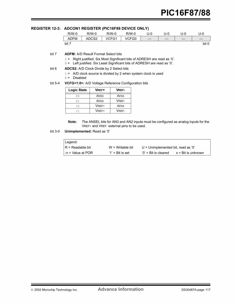
PIC16F87/88
REGISTER 12-3: ADCON1 REGISTER (PIC16F88 DEVICE ONLY)R/W-0 R/W-0 R/W-0 R/W-0 U-0 U-0 U-0 U-0ADFM ADCS2 VCFG1 VCFG0 — — — —
bit 7 bit 0
bit 7 ADFM: A/D Result Format Select bits1 = Right justified. Six Most Significant bits of ADRESH are read as ‘0’.0 = Left justified. Six Least Significant bits of ADRESH are read as ‘0’.
bit 6 ADCS2: A/D Clock Divide by 2 Select bits1 = A/D clock source is divided by 2 when system clock is used0 = Disabled
bit 5-4 VCFG<1:0>: A/D Voltage Reference Configuration bits
Note: The ANSEL bits for AN3 and AN2 inputs must be configured as analog inputs for theVREF+ and VREF- external pins to be used.
bit 3-0 Unimplemented: Read as ‘0’
Legend:R = Readable bit W = Writable bit U = Unimplemented bit, read as ‘0’-n = Value at POR ‘1’ = Bit is set ‘0’ = Bit is cleared x = Bit is unknown
Logic State VREF+ VREF-00 AVDD AVSS
01 AVDD VREF-
10 VREF+ AVSS
11 VREF+ VREF-
2002 Microchip Technology Inc. Advance Information DS30487A-page 117

PIC16F87/88
The ADRESH:ADRESL registers contain the result ofthe A/D conversion. When the A/D conversion is com-plete, the result is loaded into the A/D result registerpair, the GO/DONE bit (ADCON0<2>) is cleared, andA/D interrupt flag bit ADIF is set. The block diagram ofthe A/D module is shown in Figure 12-1.After the A/D module has been configured as desired,the selected channel must be acquired before the con-version is started. The analog input channels musthave their corresponding TRIS bits selected as inputs.
To determine sample time, see Section 12.1. After thissample time has elapsed the A/D conversion can bestarted.
These steps should be followed for doing an A/Dconversion:
1. Configure the A/D module:• Configure analog/digital I/O (ANSEL)• Configure voltage reference (ADCON1)• Select A/D input channel (ADCON0)• Select A/D conversion clock (ADCON0)• Turn on A/D module (ADCON0)
2. Configure A/D interrupt (if desired):• Clear ADIF bit • Set ADIE bit • Set GIE bit
3. Wait the required acquisition time.4. Start conversion:
• Set GO/DONE bit (ADCON0)5. Wait for A/D conversion to complete, by either:
• Polling for the GO/DONE bit to be cleared(with interrupts disabled); OR
• Waiting for the A/D interrupt6. Read A/D Result register pair
(ADRESH:ADRESL), clear bit ADIF if required.7. For next conversion, go to step 1 or step 2 as
required. The A/D conversion time per bit isdefined as TAD. A minimum wait of 2 TAD isrequired before the next acquisition starts.
FIGURE 12-1: A/D BLOCK DIAGRAM
(Input Voltage)
VIN
VREF+
(ReferenceVoltage)
AVDD
VCFG1:VCFG0
CHS2:CHS0
RA3/AN3/VREF+/C1OUT
RA2/AN2/VREF-
RA1/AN1
RA0/AN0
011
010
001
000A/D
Converter
VREF-
(ReferenceVoltage)
AVSS
VCFG1:VCFG0
RB6/AN5/PGC/T1CKI
RB7/AN6/PGD/T1OSI
RA4/AN4/T0CKI/C2OUT
110
101
100
DS30487A-page 118 Advance Information 2002 Microchip Technology Inc.

PIC16F87/88
12.1 A/D Acquisition Requirements For the A/D converter to meet its specified accuracy,the charge holding capacitor (CHOLD) must be allowedto fully charge to the input channel voltage level. Theanalog input model is shown in Figure 12-2. Thesource impedance (RS) and the internal samplingswitch (RSS) impedance directly affect the timerequired to charge the capacitor CHOLD. The samplingswitch (RSS) impedance varies over the device voltage(VDD), see Figure 12-2. The maximum recom-mended impedance for analog sources is 2.5 kΩ.As the impedance is decreased, the acquisition timemay be decreased. After the analog input channel isselected (changed), this acquisition must be donebefore the conversion can be started.
To calculate the minimum acquisition time,Equation 12-1 may be used. This equation assumesthat 1/2 LSb error is used (1024 steps for the A/D). The1/2 LSb error is the maximum error allowed for the A/Dto meet its specified resolution.
To calculate the minimum acquisition time, TACQ, seethe PICmicro™ Mid-Range Reference Manual(DS33023).
EQUATION 12-1: ACQUISITION TIME
FIGURE 12-2: ANALOG INPUT MODEL
TACQ
TC
TACQ
=
=======
Amplifier Settling Time + Hold Capacitor Charging Time + Temperature Coefficient
TAMP + TC + TCOFF2 µs + TC + [(Temperature -25°C)(0.05 µs/°C)] CHOLD (RIC + RSS + RS) In(1/2047)-120 pF (1 kΩ + 7 kΩ + 10 kΩ) In(0.0004885)16.47 µs2 µs + 16.47 µs + [(50°C – 25°C)(0.05 µs/°C)19.72 µs
Note 1: The reference voltage (VREF) has no effect on the equation, since it cancels itself out.
2: The charge holding capacitor (CHOLD) is not discharged after each conversion.
3: The maximum recommended impedance for analog sources is 10 kΩ. This is required to meet the pinleakage specification.
4: After a conversion has completed, a 2.0 TAD delay must complete before acquisition can begin again. During this time, the holding capacitor is not connected to the selected A/D input channel.
CPINVA
Rs ANx
5 pF
VDD
VT = 0.6V
VT = 0.6V I leakage
RIC ≤ 1k
SamplingSwitchSS RSS
CHOLD= DAC capacitance
VSS
6 V
Sampling Switch
5 V4 V3 V2 V
5 6 7 8 9 10 11
(kΩ)
VDD
= 51.2 pF± 500 nA
Legend: CPIN
VTI leakage
RICSSCHOLD
= input capacitance= threshold voltage= leakage current at the pin due to
= interconnect resistance= sampling switch= sample/hold capacitance (from DAC)
various junctions
2002 Microchip Technology Inc. Advance Information DS30487A-page 119

PIC16F87/88
12.2 Selecting the A/D ConversionClockThe A/D conversion time per bit is defined as TAD. TheA/D conversion requires 9.0 TAD per 8-bit conversion.The source of the A/D conversion clock is softwareselectable. The seven possible options for TAD are:
• 2 TOSC
• 4 TOSC
• 8 TOSC
• 16 TOSC
• 32 TOSC
• 64 TOSC • Internal A/D module RC oscillator (2 - 6 µs)
For correct A/D conversions, the A/D conversion clock(TAD) must be selected to ensure a minimum TAD timeas small as possible, but no less than 1.6 µs and notgreater than 6.4 µs.
Table 12-1 shows the resultant TAD times derived fromthe device operating frequencies and the A/D clocksource selected.
12.3 Configuring Analog Port PinsThe ADCON1, ANSEL, TRISA, and TRISB registerscontrol the operation of the A/D port pins. The port pinsthat are desired as analog inputs must have their cor-responding TRIS bits set (input). If the TRIS bit iscleared (output), the digital output level (VOH or VOL)will be converted.
The A/D operation is independent of the state of theCHS<2:0> bits and the TRIS bits.
TABLE 12-1: TAD vs. MAXIMUM DEVICE OPERATING FREQUENCIES (STANDARD DEVICES (C))
Note 1: When reading the port register, all pinsconfigured as analog input channels willread as cleared (a low level). Pins config-ured as digital inputs will convert an ana-log input. Analog levels on a digitallyconfigured input will not affect theconversion accuracy.
2: Analog levels on any pin that is defined asa digital input (including the RA4:RA0 andRB7:RB6 pins), may cause the inputbuffer to consume current out of thedevice specification.
AD Clock Source (TAD) Maximum Device Frequency
Operation ADCS<2> ADCS<1:0> Max.
2 TOSC 0 00 1.25 MHz4 TOSC 1 00 2.5 MHz8 TOSC 0 01 5 MHz16 TOSC 1 01 10 MHz32 TOSC 0 10 20 MHz64 TOSC 1 10 20 MHz
RC(1,2,3) X 11 (Note 1)Note 1: The RC source has a typical TAD time of 4 µs, but can vary between 2 - 6 µs.
2: When the device frequencies are greater than 1 MHz, the RC A/D conversion clock source is only recommended for SLEEP operation.
3: For extended voltage devices (LF), please refer to the Electrical Characteristics (Section 18.0 and Section 18.4).
DS30487A-page 120 Advance Information 2002 Microchip Technology Inc.

PIC16F87/88
12.4 A/D ConversionsClearing the GO/DONE bit during a conversion willabort the current conversion. The A/D result registerpair will NOT be updated with the partially completedA/D conversion sample. That is, the ADRESH:ADRESLregisters will continue to contain the value of the lastcompleted conversion (or the last value written to theADRESH:ADRESL registers). After the A/D conversionis aborted, a 2 TAD wait is required before the nextacquisition is started. After this 2 TAD wait, acquisitionon the selected channel is automatically started. TheGO/DONE bit can then be set to start the conversion.In Figure 12-3, after the GO bit is set, the first timesegment has a minimum of TCY and a maximum of TAD.
12.4.1 A/D RESULT REGISTERS
The ADRESH:ADRESL register pair is the locationwhere the 10-bit A/D result is loaded at the completionof the A/D conversion. This register pair is 16-bits wide.The A/D module gives the flexibility to left or right justifythe 10-bit result in the 16-bit result register. The A/DFormat Select bit (ADFM) controls this justification.Figure 12-4 shows the operation of the A/D result justi-fication. The extra bits are loaded with ‘0’s. When anA/D result will not overwrite these locations (A/D dis-able), these registers may be used as two generalpurpose 8-bit registers.
FIGURE 12-3: A/D CONVERSION TAD CYCLES
FIGURE 12-4: A/D RESULT JUSTIFICATION
Note: The GO/DONE bit should NOT be set inthe same instruction that turns on the A/D.
TAD1 TAD2 TAD3 TAD4 TAD5 TAD6 TAD7 TAD8 TAD9
Set GO bit
Holding Capacitor is Disconnected from Analog Input (typically 100 ns)
b9 b8 b7 b6 b5 b4 b3 b2
TAD10 TAD11
b1 b0
TCY to TAD
Conversion Starts
ADRES is Loaded,GO bit is Cleared,ADIF bit is Set,Holding Capacitor is Connected to Analog Input
10-bit Result
ADRESH ADRESL
0000 00
ADFM = 0
02 1 0 77
10-bit Result
ADRESH ADRESL
10-bit Result
0000 00
7 0 7 6 5 0
ADFM = 1
Right Justified Left Justified
2002 Microchip Technology Inc. Advance Information DS30487A-page 121

PIC16F87/88
12.5 A/D Operation During SLEEPThe A/D module can operate during SLEEP mode. Thisrequires that the A/D clock source be set to RC(ADCS1:ADCS0 = 11). When the RC clock source isselected, the A/D module waits one instruction cyclebefore starting the conversion. This allows the SLEEPinstruction to be executed, which eliminates all digitalswitching noise from the conversion. When the conver-sion is completed, the GO/DONE bit will be cleared andthe result loaded into the ADRES register. If the A/Dinterrupt is enabled, the device will wake-up fromSLEEP. If the A/D interrupt is not enabled, the A/D mod-ule will then be turned off, although the ADON bit willremain set.When the A/D clock source is another clock option (notRC), a SLEEP instruction will cause the present conver-sion to be aborted and the A/D module to be turned off,though the ADON bit will remain set.
Turning off the A/D places the A/D module in its lowestcurrent consumption state.
12.6 Effects of a RESETA device RESET forces all registers to their RESETstate. The A/D module is disabled and any conversionin progress is aborted. All A/D input pins are configuredas analog inputs.
The value that is in the ADRESH:ADRESL registersis not modified for a Power-on Reset. TheADRESH:ADRESL registers will contain unknown dataafter a Power-on Reset.
12.7 Use of the CCP TriggerAn A/D conversion can be started by the “special eventtrigger” of the CCP module. This requires that theCCP1M3:CCP1M0 bits (CCP1CON<3:0>) be pro-grammed as ‘1011’ and that the A/D module is enabled(ADON bit is set). When the trigger occurs, theGO/DONE bit will be set, starting the A/D conversionand the Timer1 counter will be reset to zero. Timer1 isreset to automatically repeat the A/D acquisition periodwith minimal software overhead (moving theADRESH:ADRESL to the desired location). The appro-priate analog input channel must be selected and theminimum acquisition done before the “special eventtrigger” sets the GO/DONE bit (starts a conversion).
If the A/D module is not enabled (ADON is cleared),then the “special event trigger” will be ignored by theA/D module, but will still reset the Timer1 counter.
Note: For the A/D module to operate in SLEEP,the A/D clock source must be set to RC(ADCS1:ADCS0 = 11). To perform an A/Dconversion in SLEEP, ensure the SLEEPinstruction immediately follows theinstruction that sets the GO/DONE bit.
TABLE 12-2: REGISTERS/BITS ASSOCIATED WITH A/D
Address Name Bit 7 Bit 6 Bit 5 Bit 4 Bit 3 Bit 2 Bit 1 Bit 0 Value onPOR, BOR
Value on all other RESETS
0Bh, 8Bh10Bh, 18Bh
INTCON GIE PEIE TMR0IE INTE RBIE TMR0IF INTF RBIF 0000 000x 0000 000u
0Ch PIR1 — ADIF RCIF TXIF SSPIF CCP1IF TMR2IF TMR1IF -000 0000 -000 0000
8Ch PIE1 — ADIE RCIE TXIE SSPIE CCP1IE TMR2IE TMR1IE -000 0000 -000 0000
1Eh ADRESH(1) A/D Result Register High Byte xxxx xxxx uuuu uuuu
9Eh ADRESL(1) A/D Result Register Low Byte xxxx xxxx uuuu uuuu
1Fh ADCON0(1) ADCS1 ADCS0 CHS2 CHS1 CHS0 GO/DONE — ADON 0000 00-0 0000 00-0
9Fh ADCON1(1) ADFM ADCS2 VCFG1 VCFG0 — — — — 0000 ---- 0000 ----
9Bh ANSEL(1) — AN6 AN5 AN4 AN3 AN2 AN1 AN0 -111 1111 -111 1111
05h PORTA-87PORTA-88
RA7 RA6 RA5 RA4 RA3 RA2 RA1 RA0 xxxx 0000xxx0 0000
uuuu 0000uuu0 0000
05h, 106h PORTB-87PORTB-88
RB7 RB6 RB5 RB4 RB3 RB2 RB1 RB0 xxxx xxxx00xx xxxx
uuuu uuuu00uu uuuu
85h TRISA TRISA7 TRISA6 TRISA5(1) PORTA Data Direction Register 1111 1111 1111 1111
86h, 186h TRISB TRISB7 TRISB6 TRISB5 TRISB4 TRISB3 TRISB2 TRISB1 TRISB0 1111 1111 1111 1111
Legend: x = unknown, u = unchanged, - = unimplemented, read as ‘0’. Shaded cells are not used for A/D conversion.Note 1: PIC16F88 only.
2: Pin 5 is an input only; the state of the TRISA5 bit has no effect and will always read ‘1’.
DS30487A-page 122 Advance Information 2002 Microchip Technology Inc.

PIC16F87/88
13.0 COMPARATOR MODULEThe comparator module contains two analog compara-tors. The inputs to the comparators are multiplexedwith I/O port pins RA0 through RA3, while the outputsare multiplexed to pins RA3 and RA4. The on-chipVoltage Reference (Section 14.0) can also be an inputto the comparators.
The CMCON register (Register 13-1) controls the com-parator input and output multiplexers. A block diagramof the various comparator configurations is shown inFigure 13-1.
REGISTER 13-1: CMCON REGISTER R-0 R-0 R/W-0 R/W-0 R/W-0 R/W-0 R/W-0 R/W-0
C2OUT C1OUT C2INV C1INV CIS CM2 CM1 CM0bit 7 bit 0
bit 7 C2OUT: Comparator 2 Output bitWhen C2INV = 0:1 = C2 VIN+ > C2 VIN-0 = C2 VIN+ < C2 VIN-When C2INV = 1:1 = C2 VIN+ > C2 VIN-0 = C2 VIN+ < C2 VIN-
bit 6 C1OUT: Comparator 1 Output bitWhen C1INV = 0:1 = C1 VIN+ > C1 VIN-0 = C1 VIN+ < C1 VIN-When C1INV = 1:1 = C1 VIN+ > C1 VIN-0 = C1 VIN+ < C1 VIN-
bit 5 C2INV: Comparator 2 Output Inversion bit1 = C2 output inverted0 = C2 output not inverted
bit 4 C1INV: Comparator 1 Output Inversion bit1 = C1 output inverted0 = C1 output not inverted
bit 3 CIS: Comparator Input Switch bitWhen CM2:CM0 = 001:1 = C1 VIN- connects to RA30 = C1 VIN- connects to RA0When CM2:CM0 = 010:1 = C1 VIN- connects to RA3
C2 VIN- connects to RA20 = C1 VIN- connects to RA0
C2 VIN- connects to RA1bit 2-0 CM<2:0>: Comparator Mode bits
Legend:R = Readable bit W = Writable bit U = Unimplemented bit, read as ‘0’- n = Value at POR ‘1’ = Bit is set ‘0’ = Bit is cleared x = Bit is unknown
2002 Microchip Technology Inc. Advance Information DS30487A-page 123

PIC16F87/88
13.1 Comparator ConfigurationThere are eight modes of operation for the compara-tors. The CMCON register is used to select thesemodes. Figure 13-1 shows the eight possible modes.The TRISA register controls the data direction of thecomparator pins for each mode. If the Comparatormode is changed, the comparator output level may notbe valid for the specified mode change delay shown inthe Electrical Specifications (Section 18.0).FIGURE 13-1: COMPARATOR I/O OPERATING MODES
Note: Comparator interrupts should be disabledduring a Comparator mode change.Otherwise, a false interrupt may occur.
C1RA0/AN0 VIN-
VIN+RA3/AN3Off (Read as '0')
Comparators Reset (POR Default Value)
A
A
CM2:CM0 = 000
C2RA1/AN1 VIN-
VIN+RA2/AN2Off (Read as '0')
A
A
C1RA0/AN0 VIN-
VIN+RA3/AN3C1OUT
Two Independent Comparators
A
A
CM2:CM0 = 100
C2RA1/AN1 VIN-
VIN+RA2/AN2C2OUT
A
A
C1RA0/AN0 VIN-
VIN+RA3/AN3C1OUT
Two Common Reference Comparators
A
D
CM2:CM0 = 011
C2RA1/AN1 VIN-
VIN+RA2/AN2C2OUT
A
A
C1RA0/AN0 VIN-
VIN+RA3/AN3Off (Read as '0')
One Independent Comparator
D
D
CM2:CM0 = 101
C2RA1/AN1 VIN-
VIN+RA2/AN2C2OUT
A
A
C1RA0/AN0 VIN-
VIN+RA3/AN3Off (Read as '0')
Comparators Off
D
D
CM2:CM0 = 111
C2RA1/AN1 VIN-
VIN+RA2/AN2Off (Read as '0')
D
D
C1
RA0/AN0 VIN-
VIN+RA3/AN3 C1OUT
Four Inputs Multiplexed to Two Comparators
A
A
CM2:CM0 = 010
C2
RA1/AN1 VIN-
VIN+RA2/AN2 C2OUT
A
A
From VREF Module
CIS = 0CIS = 1
CIS = 0CIS = 1
C1RA0/AN0 VIN-
VIN+RA3/AN3C1OUT
Two Common Reference Comparators with Outputs
A
D
CM2:CM0 = 110
C2RA1/AN1 VIN-
VIN+RA2/AN2C2OUT
A
A
A = Analog Input, port reads zeros always.D = Digital Input.CIS (CMCON<3>) is the Comparator Input Switch.
RA4/T0CKI
C1
RA0/AN0 VIN-
VIN+RA3/AN3 C1OUT
Three Inputs Multiplexed to Two Comparators
A
A
CM2:CM0 = 001
C2RA1/AN1 VIN-
VIN+RA2/AN2C2OUT
A
A
CIS = 0CIS = 1
DS30487A-page 124 Advance Information 2002 Microchip Technology Inc.

PIC16F87/88
13.2 Comparator OperationA single comparator is shown in Figure 13-2, along withthe relationship between the analog input levels andthe digital output. When the analog input at VIN+ is lessthan the analog input VIN-, the output of the comparatoris a digital low level. When the analog input at VIN+ isgreater than the analog input VIN-, the output of thecomparator is a digital high level. The shaded areas ofthe output of the comparator in Figure 13-2 representthe uncertainty due to input offsets and response time.13.3 Comparator ReferenceAn external or internal reference signal may be useddepending on the Comparator Operating mode. Theanalog signal present at VIN- is compared to the signalat VIN+, and the digital output of the comparator isadjusted accordingly (Figure 13-2).
FIGURE 13-2: SINGLE COMPARATOR
13.3.1 EXTERNAL REFERENCE SIGNAL
When external voltage references are used, thecomparator module can be configured to have the com-parators operate from the same, or different referencesources. However, threshold detector applications mayrequire the same reference. The reference signal mustbe between VSS and VDD, and can be applied to eitherpin of the comparator(s).
13.3.2 INTERNAL REFERENCE SIGNAL
The comparator module also allows the selection of aninternally generated voltage reference for thecomparators. Section 14.0 contains a detailed descrip-tion of the Comparator Voltage Reference module thatprovides this signal. The internal reference signal isused when comparators are in mode CM<2:0> = 110(Figure 13-1). In this mode, the internal voltagereference is applied to the VIN+ pin of bothcomparators.
13.4 Comparator Response TimeResponse time is the minimum time, after selecting anew reference voltage or input source, before thecomparator output has a valid level. If the internal ref-erence is changed, the maximum delay of the internalvoltage reference must be considered when using thecomparator outputs. Otherwise, the maximum delay ofthe comparators should be used (Section 18.0).
13.5 Comparator OutputsThe comparator outputs are read through the CMCONregister. These bits are read only. The comparatoroutputs may also be directly output to the RA3 and RA4I/O pins. When enabled, multiplexors in the output pathof the RA3 and RA4 pins will switch and the output ofeach pin will be the unsynchronized output of the com-parator. The uncertainty of each of the comparators isrelated to the input offset voltage and the response timegiven in the specifications. Figure 13-3 shows thecomparator output block diagram.
The TRISA bits will still function as an outputenable/disable for the RA3 and RA4 pins while in thismode.
The polarity of the comparator outputs can be changedusing the C2INV and C1INV bits (CMCON<4:5>).
–
+VIN+
VIN-Output
VIN–
VIN+
OutputOutput
VIN+
VIN-
Note 1: When reading the PORT register, all pinsconfigured as analog inputs will read as a‘0’. Pins configured as digital inputs willconvert an analog input, according to theSchmitt Trigger input specification.
2: Analog levels, on any pin defined as adigital input, may cause the input buffer toconsume more current than is specified.
2002 Microchip Technology Inc. Advance Information DS30487A-page 125

PIC16F87/88
FIGURE 13-3: COMPARATOR OUTPUT BLOCK DIAGRAM13.6 Comparator InterruptsThe comparator interrupt flag is set whenever there isa change in the output value of either comparator.Software will need to maintain information about thestatus of the output bits, as read from CMCON<7:6>, todetermine the actual change that occurred. The CMIFbit (PIR registers) is the comparator interrupt flag. TheCMIF bit must be reset by clearing it (‘0’). Since it isalso possible to write a '1' to this register, a simulatedinterrupt may be initiated.
The CMIE bit (PIE registers) and the PEIE bit (INTCONregister) must be set to enable the interrupt. In addition,the GIE bit must also be set. If any of these bits areclear, the interrupt is not enabled, though the CMIF bitwill still be set if an interrupt condition occurs.
The user, in the Interrupt Service Routine, can clear theinterrupt in the following manner:
a) Any read or write of CMCON will end themismatch condition.
b) Clear flag bit CMIF.
A mismatch condition will continue to set flag bit CMIF.Reading CMCON will end the mismatch condition, andallow flag bit CMIF to be cleared.
DQ
ENRD_CMCON
Set CMIF bit
MULTIPLEX
DQ
EN
CL
Port Pins
Q3 * RD_CMCON
NRESETFrom other Comparator
To Data Bus
Q1
CnINV
Note: If a change in the CMCON register(C1OUT or C2OUT) should occur when aread operation is being executed (start ofthe Q2 cycle), then the CMIF (PIRregisters) interrupt flag may not get set.
DS30487A-page 126 Advance Information 2002 Microchip Technology Inc.

PIC16F87/88
13.7 Comparator Operation DuringSLEEPWhen a comparator is active and the device is placedin SLEEP mode, the comparator remains active andthe interrupt is functional, if enabled. This interrupt willwake-up the device from SLEEP mode when enabled.While the comparator is powered up, higher SLEEPcurrents than shown in the power-down currentspecification will occur. Each operational comparatorwill consume additional current, as shown in the com-parator specifications. To minimize power consumptionwhile in SLEEP mode, turn off the comparators,CM<2:0> = 111, before entering SLEEP. If the devicewakes up from SLEEP, the contents of the CMCONregister are not affected.
13.8 Effects of a RESETA device RESET forces the CMCON register to itsRESET state, causing the comparator module to be inthe Comparator Off mode, CM<2:0> = 111.
13.9 Analog Input ConnectionConsiderations
A simplified circuit for an analog input is shown inFigure 13-4. Since the analog pins are connected to adigital output, they have reverse biased diodes to VDDand VSS. The analog input, therefore, must be betweenVSS and VDD. If the input voltage deviates from thisrange by more than 0.6V in either direction, one of thediodes is forward biased and a latchup condition mayoccur. A maximum source impedance of 10 kΩ is rec-ommended for the analog sources. Any external com-ponent connected to an analog input pin, such as acapacitor or a Zener diode, should have very littleleakage current.
FIGURE 13-4: ANALOG INPUT MODEL
VA
RS < 10K
AINCPIN5 pF
VDD
VT = 0.6V
VT = 0.6V
RIC
ILEAKAGE±500 nA
VSS
Legend: CPIN = Input CapacitanceVT = Threshold VoltageILEAKAGE = Leakage Current at the pin due to various junctionsRIC = Interconnect ResistanceRS = Source ImpedanceVA = Analog Voltage
2002 Microchip Technology Inc. Advance Information DS30487A-page 127

PIC16F87/88
TABLE 13-1: REGISTERS ASSOCIATED WITH THE COMPARATOR MODULEAddress Name Bit 7 Bit 6 Bit 5 Bit 4 Bit 3 Bit 2 Bit 1 Bit 0 Value onPOR
Value onall otherRESETS
9Ch CMCON C2OUT C1OUT C2INV C1INV CIS CM2 CM1 CM0 0000 0111 0000 0111
9Dh CVRCON CVREN CVROE CVRR — CVR3 CVR2 CVR1 CVR0 000- 0000 000- 0000
0Bh, 8Bh, 10Bh, 18Bh
INTCON GIE PEIE TMR0IE INTIE RBIE TMR0IF INTIF RBIF 0000 000x 0000 000u
0Dh PIR2 OSFIF CMIF — EEIF — — — — 00-0 ---- 00-0 ----
8Dh PIE2 OSFIE CMIE — EEIE — — — — 00-0 ---- 00-0 ----
05h PORTA-87PORTA-88
RA7 RA6 RA5 RA4 RA3 RA2 RA1 RA0 xxxx 0000xxx0 0000
uuuu 0000uuu0 0000
85h TRISA TRISA7 TRISA6 TRISA5(1) TRISA4 TRISA3 TRISA2 TRISA1 TRISA0 1111 1111 1111 1111
Legend: x = unknown, u = unchanged, - = unimplemented, read as ‘0’. Shaded cells are unused by the comparator module.Note 1: Pin 5 is an input only; the state of the TRISA5 bit has no effect and will always read ‘1’.
DS30487A-page 128 Advance Information 2002 Microchip Technology Inc.

PIC16F87/88
14.0 COMPARATOR VOLTAGE REFERENCE MODULE
The Comparator Voltage Reference Generator is a16-tap resistor ladder network that provides a fixedvoltage reference when the comparators are in mode‘110’. A programmable register controls the function ofthe reference generator. Register 14-1 lists the bitfunctions of the CVRCON register.
As shown in Figure 14-1, the resistor ladder is seg-mented to provide two ranges of CVREF values and hasa power-down function to conserve power when thereference is not being used. The comparator reference
supply voltage (also referred to as CVRSRC) comesdirectly from VDD. It should be noted, however, that thevoltage at the top of the ladder is CVRSRC – VSAT,where VSAT is the saturation voltage of the powerswitch transistor. This reference will only be asaccurate as the values of CVRSRC and VSAT.
The output of the reference generator may be con-nected to the RA2/AN2/VREF-/CVREF pin. This can beused as a simple D/A function by the user, if a very highimpedance load is used. The primary purpose of thisfunction is to provide a test path for testing thereference generator function.
REGISTER 14-1: CVRCON CONTROL REGISTER
R/W-0 R/W-0 R/W-0 U-0 R/W-0 R/W-0 R/W-0 R/W-0CVREN CVROE CVRR — CVR3 CVR2 CVR1 CVR0
bit 7 bit 0
bit 7 CVREN: Comparator Voltage Reference Enable bit1 = CVREF circuit powered on0 = CVREF circuit powered down
bit 6 CVROE: Comparator VREF Output Enable bit1 = CVREF voltage level is output on RA2/AN2/VREF-/CVREF pin0 = CVREF voltage level is disconnected from RA2/AN2/VREF-/CVREF pin
bit 5 CVRR: Comparator VREF Range Selection bit1 = 0.00 CVRSRC to 0.75 CVRSRC, with CVRSRC/24 step size 0 = 0.25 CVRSRC to 0.75 CVRSRC, with CVRSRC/32 step size
bit 4 Unimplemented: Read as ‘0’ bit 3-0 CVR<3:0>: Comparator VREF Value Selection 0 ≤ VR3:VR0 ≤ 15 bits
When CVRR = 1: CVREF = (VR<3:0>/ 24) • (CVRSRC)When CVRR = 0: CVREF = 1/4 • (CVRSRC) + (VR3:VR0/ 32) • (CVRSRC)
Legend:R = Readable bit W = Writable bit U = Unimplemented bit, read as ‘0’-n = Value at POR ‘1’ = Bit is set ‘0’ = Bit is cleared x = Bit is unknown
2002 Microchip Technology Inc. Advance Information DS30487A-page 129

PIC16F87/88
FIGURE 14-1: COMPARATOR VOLTAGE REFERENCE BLOCK DIAGRAMTABLE 14-1: REGISTERS ASSOCIATED WITH COMPARATOR VOLTAGE REFERENCE
CVRR8R
CVR3
CVR0
16 - 1 Analog MUX
8R R R R RCVREN
CVREF
16 Stages
Input toComparator
CVROE
RA2/AN2/VREF-/CVREF pin
VDD
CVR2CVR1
Address Name Bit 7 Bit 6 Bit 5 Bit 4 Bit 3 Bit 2 Bit 1 Bit 0 Value onPOR
Value onall otherRESETS
9Dh CVRCON CVREN CVROE CVRR — CVR3 CVR2 CVR1 CVR0 000- 0000 000- 0000
9Ch CMCON C2OUT C1OUT C2INV C1INV CIS CM2 CM1 CM0 0000 0000 0000 0000
Legend: x = unknown, u = unchanged, - = unimplemented, read as ‘0’. Shaded cells are not used with the comparator voltage reference.
DS30487A-page 130 Advance Information 2002 Microchip Technology Inc.

PIC16F87/88
15.0 SPECIAL FEATURES OF THE CPU
These devices have a host of features intended to max-imize system reliability, minimize cost through elimina-tion of external components, provide Power SavingOperating modes and offer code protection:
• RESET- Power-on Reset (POR)- Power-up Timer (PWRT)- Oscillator Start-up Timer (OST)- Brown-out Reset (BOR)
• Interrupts• Watchdog Timer (WDT)• Two-Speed Start-up• Fail-Safe Clock Monitor• SLEEP• Code Protection• ID Locations• In-Circuit Serial Programming
There are two timers that offer necessary delays onpower-up. One is the Oscillator Start-up Timer (OST),intended to keep the chip in RESET until the crystaloscillator is stable. The other is the Power-up Timer(PWRT), which provides a fixed delay of 72 ms (nomi-nal) on power-up only. It is designed to keep the part inRESET while the power supply stabilizes, and isenabled or disabled using a configuration bit. Withthese two timers on-chip, most applications need noexternal RESET circuitry.
SLEEP mode is designed to offer a very low currentPower-down mode. The user can wake-up fromSLEEP through external RESET, Watchdog TimerWake-up, or through an interrupt.
Several oscillator options are also made available toallow the part to fit the application. The RC oscillatoroption saves system cost while the LP crystal optionsaves power. Configuration bits are used to select thedesired Oscillator mode.
Additional information on special features is availablein the PICmicro® Mid-Range Reference Manual(DS33023).
15.1 Configuration BitsThe configuration bits can be programmed (read as‘0’), or left unprogrammed (read as ‘1’), to select vari-ous device configurations. These bits are mapped inprogram memory locations 2007h and 2008h.
The user will note that address 2007h is beyond theuser program memory space, which can be accessedonly during programming.
2002 Microchip Technology Inc. Advance Information DS30487A-page 131

PIC16F87/88
REGISTER 15-1: CONFIGURATION WORD 1 REGISTER (ADDRESS 2007h)R/P-1 R/P-1 R/P-1 R/P-1 R/P-1 R/P-1 R/P-1 R/P-1 R/P-1 R/P-1 R/P-1 R/P-1 R/P-1 R/P-1CP CCPMX RESV WRT1 WRT0 CPD LVP BOREN MCLRE FOSC2 PWRTEN WDTEN FOSC1 FOSC0
bit 13 bit 0
bit 13 CP: FLASH Program Memory Code Protection bits1 = Code protection off0 = 0000h to 0FFFh code protected (All protected)
bit 12 CCPMX: CCP1 Pin Selection bit1 = CCP1 function on RB00 = CCP1 function on RB3
bit 11 DEBUG: In-Circuit Debugger Mode bit1 = In-Circuit Debugger disabled, RB6 and RB7 are general purpose I/O pins0 = In-Circuit Debugger enabled, RB6 and RB7 are dedicated to the debugger
bit 10-9 WRT<1:0>: FLASH Program Memory Write Enable bits11 = Write protection off10 = 0000h to 00FFh write protected, 0100h to 0FFFh may be modified by EECON control01 = 0000h to 07FFh write protected, 0800h to 0FFFh may be modified by EECON control00 = 0000h to 0FFFh write protected
bit 8 CPD: Data EE Memory Code Protection bit1 = Code protection off 0 = Data EE memory code protected
bit 7 LVP: Low Voltage Programming Enable bit1 = RB3/PGM pin has PGM function, low voltage programming enabled0 = RB3 is digital I/O, HV on MCLR must be used for programming
bit 6 BOREN: Brown-out Reset Enable bit1 = BOR enabled0 = BOR disabled
bit 5 MCLRE: RA5/MCLR Pin Function Select bit1 = RA5/MCLR pin function is MCLR0 = RA5/MCLR pin function is digital I/O, MCLR internally tied to VDD
bit 3 PWRTEN: Power-up Timer Enable bit1 = PWRT disabled0 = PWRT enabled
bit 2 WDTEN: Watchdog Timer Enable bit1 = WDT enabled0 = WDT disabled
bit 4, 1-0 FOSC<2:0>: Oscillator Selection bits111 = EXTRC oscillator; CLKO function on RA6/OSC2/CLKO110 = EXTRC oscillator; Port I/O function on RA6/OSC2/CLKO101 = INTRC oscillator; CLKO function on RA6/OSC2/CLKO100 = INTRC oscillator; Port I/O function on RA6/OSC2/CLKO011 = EXTCLK; Port I/O function on RA6/OSC2/CLKO010 = HS oscillator001 = XT oscillator000 = LP oscillator
Legend:R = Readable bit W = Writable bit U = Unimplemented bit, read as ‘0’-n = Value at POR ‘1’ = Bit is set ‘0’ = Bit is cleared x = Bit is unknown
DS30487A-page 132 Advance Information 2002 Microchip Technology Inc.

PIC16F87/88
REGISTER 15-2: CONFIGURATION WORD 2 REGISTER (ADDRESS 2008h)U-1 U-1 U-1 U-1 U-1 U-1 U-1 U-1 U-1 U-1 U-1 U-1 R/P-1 R/P-1— — — — — — — — — — — — IESO FCMEN
bit 13 bit 0
bit 13-2 Unimplemented: Read as ‘1’bit 1 IESO: Internal External Switch Over bit
1 = Internal External Switch Over mode enabled0 = Internal External Switch Over mode disabled
bit 0 FCMEN: Fail Clock Monitor Enable bit1 = Fail-Safe Clock Monitor enabled0 = Fail-Safe Clock Monitor disabled
Legend:R = Readable bit W = Writable bit U = Unimplemented bit, read as ‘0’-n = Value at POR ‘1’ = Bit is set ‘0’ = Bit is cleared x = Bit is unknown
2002 Microchip Technology Inc. Advance Information DS30487A-page 133

PIC16F87/88
15.2 RESETThe PIC16F87/88 differentiates between various kindsof RESET:• Power-on Reset (POR)• MCLR Reset during normal operation• MCLR Reset during SLEEP• WDT Reset during normal operation• WDT Wake-up during SLEEP• Brown-out Reset (BOR)
Some registers are not affected in any RESET condi-tion. Their status is unknown on POR and unchangedin any other RESET. Most other registers are reset to a“RESET state” on Power-on Reset (POR), on theMCLR and WDT Reset, on MCLR Reset duringSLEEP, and Brown-out Reset (BOR). They are notaffected by a WDT wake-up, which is viewed as theresumption of normal operation. The TO and PD bitsare set or cleared differently in different RESET situa-tions, as indicated in Table 15-3. These bits are used insoftware to determine the nature of the RESET. Upona POR, BOR, or wake-up from SLEEP, the CPUrequires approximately 5 - 10 µs to become ready forcode execution. This delay runs in parallel with anyother timers. See Table 15-4 for a full description ofRESET states of all registers.
A simplified block diagram of the on-chip RESET circuitis shown in Figure 15-1.
FIGURE 15-1: SIMPLIFIED BLOCK DIAGRAM OF ON-CHIP RESET CIRCUIT
S
R Q
ExternalRESET
MCLR
VDD
OSC1
WDTModule
VDD RiseDetect
OST/PWRT
INTRC
WDT
Time-out
Power-on Reset
OST
10-bit Ripple Counter
PWRT
Chip_Reset
11-bit Ripple Counter
Reset
Enable OST
Enable PWRT
SLEEP
Brown-outReset
BOREN
31.25 kHz
DS30487A-page 134 Advance Information 2002 Microchip Technology Inc.

PIC16F87/88
15.3 MCLR PIC16F87/88 devices have a noise filter in the MCLRReset path. The filter will detect and ignore smallpulses.
It should be noted that a WDT Reset does not driveMCLR pin low.
The behavior of the ESD protection on the MCLR pinhas been altered from previous devices of this family.Voltages applied to the pin that exceed its specification,can result in both MCLR and excessive current beyondthe device specification, during the ESD event. For thisreason, Microchip recommends that the MCLR pin nolonger be tied directly to VDD. The use of anRC network, as shown in Figure 15-2, is suggested.
The RA5/MCLR pin can be configured for MCLR(default), or as an I/O pin (RA5). This is configuredthrough the MCLRE bit in Configuration Word 1.
FIGURE 15-2: RECOMMENDED MCLR CIRCUIT
15.4 Power-on Reset (POR)A Power-on Reset pulse is generated on-chip whenVDD rise is detected (in the range of 1.2V - 1.7V). Totake advantage of the POR, tie the MCLR pin to VDD,as described in Section 15.3. A maximum risetime for VDD is specified. See Section 18.0, "ElectricalCharacteristics" for details.
When the device starts normal operation (exits theRESET condition), device operating parameters (volt-age, frequency, temperature,...) must be met to ensureoperation. If these conditions are not met, the devicemust be held in RESET until the operating conditionsare met. For more information, see Application Note,AN607 “Power-up Trouble Shooting” (DS00607).
15.5 Power-up Timer (PWRT)The Power-up Timer (PWRT) of the PIC16F87/88 is acounter that uses the INTRC oscillator as the clockinput. This yields a count of 72 ms. While the PWRT iscounting, the device is held in RESET.
The power-up time delay depends on the INTRC, andwill vary from chip-to-chip due to temperature andprocess variation. See DC parameter #33 for details.
The PWRT is enabled by clearing configuration bitPWRTEN.
15.6 Oscillator Start-up Timer (OST)The Oscillator Start-up Timer (OST) provides 1024oscillator cycles (from OSC1 input) delay after thePWRT delay is over (if enabled). This helps to ensurethat the crystal oscillator or resonator has started andstabilized.
The OST time-out is invoked only for XT, LP and HSmodes and only on Power-on Reset, or wake-up fromSLEEP.
15.7 Brown-out Reset (BOR)The configuration bit, BOREN, can enable or disablethe Brown-out Reset circuit. If VDD falls below VBOR(parameter D005, about 4V) for longer than TBOR(parameter #35, about 100 µs), the brown-out situationwill reset the device. If VDD falls below VBOR for lessthan TBOR, a RESET may not occur.
Once the brown-out occurs, the device will remain inBrown-out Reset until VDD rises above VBOR. ThePower-up Timer (if enabled) will keep the device inRESET for TPWRT (parameter #33, about 72 ms). IfVDD should fall below VBOR during TPWRT, the Brown-out Reset process will restart when VDD rises aboveVBOR, with the Power-up Timer Reset. Unlike previousPIC16 devices, the PWRT is no longer automaticallyenabled when the Brown-out Reset circuit is enabled.The PWRTEN and BOREN configuration bits areindependent of each other.
C10.1 µF
R11 kΩ (or greater)
(optional, not critical)
VDD
MCLR
PIC16F87/88
2002 Microchip Technology Inc. Advance Information DS30487A-page 135

PIC16F87/88
15.8 Time-out SequenceOn power-up, the time-out sequence is as follows: thePWRT delay starts (if enabled) when a POR occurs.Then, OST starts counting 1024 oscillator cycles whenPWRT ends (LP, XT, HS). When the OST ends, thedevice comes out of RESET.
If MCLR is kept low long enough, all delays will expire.Bringing MCLR high will begin execution immediately.This is useful for testing purposes, or to synchronizemore than one PIC16F87/88 device operating inparallel.
Table 15-3 shows the RESET conditions for theSTATUS, PCON and PC registers, while Table 15-4shows the RESET conditions for all the registers.
15.9 Power Control/Status Register (PCON)
The Power Control/Status Register, PCON, has twobits to indicate the type of RESET that last occurred.
Bit0 is Brown-out Reset Status bit, BOR. Bit BOR isunknown on a Power-on Reset. It must then be set bythe user and checked on subsequent RESETS to seeif bit BOR cleared, indicating a Brown-out Resetoccurred. When the Brown-out Reset is disabled, thestate of the BOR bit is unpredictable.
Bit1 is POR (Power-on Reset Status bit). It is cleared ona Power-on Reset and unaffected otherwise. The usermust set this bit following a Power-on Reset.
TABLE 15-1: TIME-OUT IN VARIOUS SITUATIONS
TABLE 15-2: STATUS BITS AND THEIR SIGNIFICANCE
Oscillator ConfigurationPower-up Brown-out Reset Wake-up from
SLEEPPWRTE = 0 PWRTE = 1 PWRTE = 0 PWRTE = 1XT, HS, LP TPWRT +
1024 • TOSC1024 • TOSC TPWRT +
1024 • TOSC1024 • TOSC 1024 • TOSC
EXTRC, INTRC TPWRT 5 - 10 µs(1) TPWRT 5 - 10 µs(1) 5 - 10 µs(1)
T1OSC — — — — 5 - 10 µs(1)
Note 1: CPU start-up is always invoked on POR, BOR and wake-up from SLEEP. The 5 µs - 10 µs delay is basedon a 1 MHz System Clock.
POR BOR TO PD
0 x 1 1 Power-on Reset0 x 0 x Illegal, TO is set on POR0 x x 0 Illegal, PD is set on POR1 0 1 1 Brown-out Reset1 1 0 1 WDT Reset 1 1 0 0 WDT Wake-up1 1 u u MCLR Reset during normal operation1 1 1 0 MCLR Reset during SLEEP or Interrupt Wake-up from SLEEP
Legend: u = unchanged, x = unknown
DS30487A-page 136 Advance Information 2002 Microchip Technology Inc.

PIC16F87/88
TABLE 15-3: RESET CONDITION FOR SPECIAL REGISTERSCondition ProgramCounter
STATUSRegister
PCONRegister
Power-on Reset 000h 0001 1xxx ---- --0xMCLR Reset during normal operation 000h 000u uuuu ---- --uuMCLR Reset during SLEEP 000h 0001 0uuu ---- --uuWDT Reset 000h 0000 1uuu ---- --uuWDT Wake-up PC + 1 uuu0 0uuu ---- --uuBrown-out Reset 000h 0001 1uuu ---- --u0Interrupt Wake-up from SLEEP PC + 1(1) uuu1 0uuu ---- --uuLegend: u = unchanged, x = unknown, - = unimplemented bit, read as '0'Note 1: When the wake-up is due to an interrupt and the GIE bit is set, the PC is loaded with the interrupt vector
(0004h).
TABLE 15-4: INITIALIZATION CONDITIONS FOR ALL REGISTERS
Register Power-on Reset,Brown-out Reset
MCLR Reset,WDT Reset
Wake-up via WDT or Interrupt
W xxxx xxxx uuuu uuuu uuuu uuuuINDF N/A N/A N/ATMR0 xxxx xxxx uuuu uuuu uuuu uuuuPCL 0000h 0000h PC + 1(2)
STATUS 0001 1xxx 000q quuu(3) uuuq quuu(3)
FSR xxxx xxxx uuuu uuuu uuuu uuuuPORTA xxx0 0000 uuu0 0000 uuuu uuuuPORTB xxxx xxxx uuuu uuuu uuuu uuuuPCLATH ---0 0000 ---0 0000 ---u uuuuINTCON 0000 000x 0000 000u uuuu uuuu(1)
PIR1 -000 0000 -000 0000 -uuu uuuu(1)
PIR2 00-0 ---- 00-0 ---- uu-u ----(1)
TMR1L xxxx xxxx uuuu uuuu uuuu uuuuTMR1H xxxx xxxx uuuu uuuu uuuu uuuuT1CON -000 0000 -uuu uuuu -uuu uuuuTMR2 0000 0000 0000 0000 uuuu uuuuT2CON -000 0000 -000 0000 -uuu uuuuSSPBUF xxxx xxxx uuuu uuuu uuuu uuuuSSPCON 0000 0000 0000 0000 uuuu uuuuCCPR1L xxxx xxxx uuuu uuuu uuuu uuuuCCPR1H xxxx xxxx uuuu uuuu uuuu uuuuCCP1CON --00 0000 --00 0000 --uu uuuuRCSTA 0000 000x 0000 000x uuuu uuuuTXREG 0000 0000 0000 0000 uuuu uuuuRCREG 0000 0000 0000 0000 uuuu uuuuADRESH xxxx xxxx uuuu uuuu uuuu uuuuADCON0 0000 00-0 0000 00-0 uuuu uu-uLegend: u = unchanged, x = unknown, - = unimplemented bit, read as '0', q = value depends on condition,
r = reserved, maintain clearNote 1: One or more bits in INTCON, PIR1 and PR2 will be affected (to cause wake-up).
2: When the wake-up is due to an interrupt and the GIE bit is set, the PC is loaded with the interrupt vector (0004h).
3: See Table 15-3 for RESET value for specific condition.
2002 Microchip Technology Inc. Advance Information DS30487A-page 137

PIC16F87/88
FIGURE 15-3: TIME-OUT SEQUENCE ON POWER-UP (MCLR TIED TO VDD THROUGH PULL-UP RESISTOR)
OPTION 1111 1111 1111 1111 uuuu uuuuTRISA 1111 1111 1111 1111 uuuu uuuuTRISB 1111 1111 1111 1111 uuuu uuuuPIE1 -000 0000 -000 0000 -uuu uuuuPIE2 00-0 ---- 00-0 ---- uu-u ----PCON ---- --qq ---- --uu ---- --uuOSCCON -000 0000 -000 0000 -uuu uuuuOSCTUNE --00 0000 --00 0000 --uu uuuuPR2 1111 1111 1111 1111 1111 1111SSPADD 0000 0000 0000 0000 uuuu uuuuSSPSTAT 0000 0000 0000 0000 uuuu uuuuTXSTA 0000 -010 0000 -010 uuuu -u1uSPBRG 0000 0000 0000 0000 uuuu uuuuANSEL -111 1111 -111 1111 -111 1111CMCON 0000 0000 0000 0000 uuuu uuuuCVRCON 000- 0000 000- 0000 uuu- uuuuWDTCON ---0 1000 ---0 1000 ---u 1uuuADRESL xxxx xxxx uuuu uuuu uuuu uuuuADCON1 0000 ---- 0000 ---- uuuu ----EEDATA xxxx xxxx uuuu uuuu uuuu uuuuEEADR xxxx xxxx uuuu uuuu uuuu uuuuEEDATH --xx xxxx --uu uuuu --uu uuuuEEADRH ---- -xxx ---- -uuu ---- -uuuEECON1 x--x x000 u--x u000 u--u uuuuEECON2 ---- ---- ---- ---- ---- ----
TABLE 15-4: INITIALIZATION CONDITIONS FOR ALL REGISTERS (CONTINUED)
Register Power-on Reset,Brown-out Reset
MCLR Reset,WDT Reset
Wake-up via WDT or Interrupt
Legend: u = unchanged, x = unknown, - = unimplemented bit, read as '0', q = value depends on condition, r = reserved, maintain clear
Note 1: One or more bits in INTCON, PIR1 and PR2 will be affected (to cause wake-up).2: When the wake-up is due to an interrupt and the GIE bit is set, the PC is loaded with the interrupt vector
(0004h).3: See Table 15-3 for RESET value for specific condition.
TPWRT
TOST
VDD
MCLR
INTERNAL POR
PWRT TIME-OUT
OST TIME-OUT
INTERNAL RESET
DS30487A-page 138 Advance Information 2002 Microchip Technology Inc.

PIC16F87/88
FIGURE 15-4: TIME-OUT SEQUENCE ON POWER-UP (MCLR TIED TO VDD THROUGHRC NETWORK): CASE 1
FIGURE 15-5: TIME-OUT SEQUENCE ON POWER-UP (MCLR TIED TO VDD THROUGHRC NETWORK): CASE 2
FIGURE 15-6: SLOW RISE TIME (MCLR TIED TO VDD THROUGH RC NETWORK)
TPWRT
TOST
VDD
MCLR
INTERNAL POR
PWRT TIME-OUT
OST TIME-OUT
INTERNAL RESET
VDD
MCLR
INTERNAL POR
PWRT TIME-OUT
OST TIME-OUT
INTERNAL RESET
TPWRT
TOST
VDD
MCLR
INTERNAL POR
PWRT TIME-OUT
OST TIME-OUT
INTERNAL RESET
0V 1V
5V
TPWRT
TOST
2002 Microchip Technology Inc. Advance Information DS30487A-page 139

PIC16F87/88
15.10 InterruptsThe PIC16F87/88 has up to 12 sources of interrupt.The Interrupt Control register (INTCON) records indi-vidual interrupt requests in flag bits. It also hasindividual and global interrupt enable bits.A global interrupt enable bit, GIE (INTCON<7>),enables (if set) all unmasked interrupts, or disables (ifcleared) all interrupts. When bit GIE is enabled, and aninterrupt’s flag bit and mask bit are set, the interrupt willvector immediately. Individual interrupts can be dis-abled through their corresponding enable bits in vari-ous registers. Individual interrupt bits are setregardless of the status of the GIE bit. The GIE bit iscleared on RESET.
The “return from interrupt” instruction, RETFIE, exitsthe interrupt routine, as well as sets the GIE bit, whichre-enables interrupts.
The RB0/INT pin interrupt, the RB port change interruptand the TMR0 overflow interrupt flags are contained inthe INTCON register.
The peripheral interrupt flags are contained in the Spe-cial Function Register, PIR1. The corresponding inter-rupt enable bits are contained in Special FunctionRegister, PIE1, and the peripheral interrupt enable bitis contained in Special Function Register, INTCON.
When an interrupt is serviced, the GIE bit is cleared todisable any further interrupt, the return address ispushed onto the stack, and the PC is loaded with0004h. Once in the Interrupt Service Routine, thesource(s) of the interrupt can be determined by pollingthe interrupt flag bits. The interrupt flag bit(s) must becleared in software before re-enabling interrupts toavoid recursive interrupts.
For external interrupt events, such as the INT pin orPORTB change interrupt, the interrupt latency will bethree or four instruction cycles. The exact latencydepends on when the interrupt event occurs, relative tothe current Q cycle. The latency is the same for one ortwo cycle instructions. Individual interrupt flag bits areset, regardless of the status of their correspondingmask bit, PEIE bit, or the GIE bit.
FIGURE 15-7: INTERRUPT LOGIC
Note: Individual interrupt flag bits are set, regard-less of the status of their correspondingmask bit or the GIE bit.
OSFIFOSFIE
ADIFADIE
RCIFRCIE
TXIFTXIE
SSPIFSSPIE
TMR2IFTMR2IE
TMR1IFTMR1IE
TMR0IFTMR0IE
INTFINTE
RBIFRBIE
GIE
PEIE
Wake-up (If in SLEEP mode)
Interrupt to CPU
EEIFEEIE
CCP1IFCCP1IE
CMIECMIF
DS30487A-page 140 Advance Information 2002 Microchip Technology Inc.

PIC16F87/88
15.10.1 INT INTERRUPTExternal interrupt on the RB0/INT pin is edge-triggered,either rising, if bit INTEDG (OPTION<6>) is set, or fall-ing, if the INTEDG bit is clear. When a valid edgeappears on the RB0/INT pin, flag bit INTF(INTCON<1>) is set. This interrupt can be disabled byclearing enable bit INTE (INTCON<4>). Flag bit INTFmust be cleared in software in the Interrupt ServiceRoutine before re-enabling this interrupt. The INT inter-rupt can wake-up the processor from SLEEP, if bit INTEwas set prior to going into SLEEP. The status of globalinterrupt enable bit GIE decides whether or not theprocessor branches to the interrupt vector, followingwake-up. See Section 15.13 for details on SLEEPmode.
15.10.2 TMR0 INTERRUPT
An overflow (FFh → 00h) in the TMR0 register will setflag bit TMR0IF (INTCON<2>). The interrupt can beenabled/disabled by setting/clearing enable bitTMR0IE (INTCON<5>), see Section 6.0.
15.10.3 PORTB INTCON CHANGE
An input change on PORTB<7:4> sets flag bit RBIF(INTCON<0>). The interrupt can be enabled/disabledby setting/clearing enable bit RBIE (INTCON<4>), seeSection 3.2.
15.11 Context Saving During InterruptsDuring an interrupt, only the return PC value is savedon the stack. Typically, users may wish to save key reg-isters during an interrupt (i.e., W, STATUS registers).This will have to be implemented in software, as shownin Example 15-1.
For the PIC16F87/88 devices, the register W_TEMPmust be defined in both banks 0 and 1 and must bedefined at the same offset from the bank base address(i.e., if W_TEMP is defined at 20h in bank 0, it must alsobe defined at A0h in bank 1). The registerSTATUS_TEMP is only defined in bank 0.
EXAMPLE 15-1: SAVING STATUS AND W REGISTERS IN RAM MOVWF W_TEMP ;Copy W to TEMP registerSWAPF STATUS,W ;Swap status to be saved into W CLRF STATUS ;bank 0, regardless of current bank, Clears IRP,RP1,RP0MOVWF STATUS_TEMP ;Save status to bank zero STATUS_TEMP register::(ISR) ;Insert user code here:SWAPF STATUS_TEMP,W ;Swap STATUS_TEMP register into W
;(sets bank to original state)MOVWF STATUS ;Move W into STATUS registerSWAPF W_TEMP,F ;Swap W_TEMPSWAPF W_TEMP,W ;Swap W_TEMP into W
2002 Microchip Technology Inc. Advance Information DS30487A-page 141

PIC16F87/88
15.12 Watchdog Timer (WDT)For PIC16F87/88 devices, the WDT has been modifiedfrom previous PIC16 devices. The new WDT is codeand functionally backward compatible with previousPIC16 WDT modules, and allows the user to have ascaler value for the WDT and TMR0 at the same time.In addition, the WDT time-out value can be extended to268 seconds, using the prescaler with the postscalerwhen PSA is set to ‘1’.15.12.1 WDT OSCILLATOR
The WDT derives its time-base from the 31.25 kHzINTRC; therefore, the accuracy of the 31.25 kHz will bethe same accuracy for the WDT time-out period.
A new prescaler has been added to the path betweenthe internal RC and the multiplexors used to select thepath for the WDT. This prescaler is 16-bits and can beprogrammed to divide the internal RC by 128 to 65536,giving the time-base used for the WDT a nominal rangeof 1 ms to 2.097s.
15.12.2 WDT CONTROL
The WDTEN bit is located in Configuration Word 1 andwhen this bit is set, the WDT runs continuously.
The SWDTEN bit is in the WDTCON register. When theWDTEN bit in the Configuration Word 1 register is set,the SWDTEN bit has no effect. If WDTEN is clear, thenthe SWDTEN bit can be used to enable and disable theWDT. Setting the bit will enable it and clearing the bitwill disable it.
The PSA and PS<2:0> bits (OPTION_REG) have thesame function as in previous versions of the PIC16family of microcontrollers.
15.12.3 RESET STATE
The value of WDTCON is ‘---0 1000’ on all RESETS.This gives a nominal time-base of 16.38 ms, which iscompatible with the time-base generated with previousPIC16 microcontroller versions.
FIGURE 15-8: WATCHDOG TIMER BLOCK DIAGRAM
Note: When the OST is invoked, the WDT is heldin RESET, because the WDT RippleCounter is used by the OST to perform theoscillator delay count. When the OSTcount has expired, the WDT will begincounting (if enabled).
TABLE 15-5: PRESCALER/POSTSCALER BIT STATUS
Conditions Prescaler Postscaler (PSA = 1)WDTEN = 0
Cleared ClearedCLRWDT commandOSC FAIL detectedExit SLEEP + System Clock = T1OSC, EXTRC, INTRC, EXTCLKExit SLEEP + System Clock = XT, HS, LP Cleared at end of OST Cleared at end of OST
31.25 kHz
PSA
16-bit Programmable Prescaler WDT
From TMR0 Clock Source
Postscaler
8
PS<2:0>
PSA
WDT Time-out
TO TMR0WDTPS<3:0>
WDTEN from Configuration Word
1
10
0
SWDTEN from WDTCON
INTRC Clock
DS30487A-page 142 Advance Information 2002 Microchip Technology Inc.

PIC16F87/88
REGISTER 15-3: WDTCON REGISTERTABLE 15-6: SUMMARY OF WATCHDOG TIMER REGISTERS
U-0 U-0 U-0 R/W-0 R/W-1 R/W-0 R/W-0 R/W-0— — — WDTPS3 WDTPS2 WDTPS1 WDTPS0 SWDTEN
bit 7 bit 0
bit 7-5 Unimplemented: Read as '0'bit 4-1 WDTPS<3:0>: Watchdog Timer Period Select bits
Bit Value Prescale Rate0000 = 1:320001 = 1:640010 = 1:1280011 = 1:2560100 = 1:5120101 = 1:10240110 = 1:20480111 = 1:40961000 = 1:81921001 = 1:163941010 = 1:327681011 = 1:65536
bit 0 SWDTEN: Software Enable/Disable for Watchdog Timer bit(1) 1 = WDT is turned on0 = WDT is turned off
Note 1: If WDTEN configuration bit = 1, then WDT is always enabled, irrespective of this con-trol bit. If WDTEN configuration bit = 0, then it is possible to turn WDT on/off with thiscontrol bit.
Legend:R = Readable bit W = Writable bit U = Unimplemented bit, read as ‘0’-n = Value at POR ‘1’ = Bit is set ‘0’ = Bit is cleared x = Bit is unknown
Address Name Bit 7 Bit 6 Bit 5 Bit 4 Bit 3 Bit 2 Bit 1 Bit 0
81h,181h OPTION RBPU INTEDG T0CS T0SE PSA PS2 PS1 PS0
2007h Configuration bits LVP BOREN MVCLRE FOSC2 PWRTEN WDTEN FOSC1 FOSC0
105h WDTCON — — — WDTPS3 WDTPS2 WSTPS1 WDTPS0 SWDTENLegend: Shaded cells are not used by the Watchdog Timer.Note 1: See Register 15-1 for operation of these bits.
2002 Microchip Technology Inc. Advance Information DS30487A-page 143

PIC16F87/88
15.12.4 TWO-SPEED CLOCK START-UPMODE
Two-Speed Start-up minimizes the latency betweenoscillator start-up and code execution that may beselected with the IESO (Internal/External Switch Over)bit in Configuration Word 2. This mode is achieved byinitially using the INTRC for code execution until theprimary oscillator is stable.
In this mode, upon
• POR and after the Power-up Timer has expired (if PWRTEN = 0),
• or following a wake-up from SLEEP, • or a RESET when running from T1OSC or INTRC
(after a RESET, SCS<1:0> are always set to ‘00’).
the system will begin execution with the INTRC oscilla-tor. This results in almost immediate code executionwith a minimum of delay.
If the primary oscillator is configured to be anythingother than XT, LP, or HS, then Two-Speed Start-up isdisabled, because the primary oscillator doesn’trequire any time to become stable after POR, or an exitfrom SLEEP.
If the IRCF bits of the OSCCON register are configuredto a non-zero value prior to entering SLEEP mode, thesecondary system clock frequency will come from theoutput of the INTOSC. The IOFS bit in the OSCCONregister will be clear until the INTOSC is stable. Thiswill allow the user to determine when the internaloscillator can be used for time critical applications.
Checking the state of the OSTS bit will confirmwhether the primary clock configuration is engaged. Ifnot, the OSTS bit will remain clear.
When the device is auto-configured in INTRC mode fol-lowing a POR or wake-up from SLEEP, the rules forentering other Oscillator modes still apply, meaning theSCS<1:0> bits in OSCCON can be modified before theOST time-out has occurred. This would allow the appli-cation to wake-up from SLEEP, perform a few instruc-tions using the INTRC as the clock source and go backto SLEEP without waiting for the primary oscillator tobecome stable.
15.12.4.1 Two-Speed Start-up Sequence1. Wake-up from SLEEP, RESET, or POR.2. OSCON bits configured to run from INTRC
(31.25 kHz).3. Instructions begin execution by INTRC
(31.25 kHz).4. OST enabled to count 1024 clock cycles.5. OST timed out, wait for falling edge of INTRC.6. OSTS is set.7. System clock held low for eight falling edges of
new clock (LP, XT, or HS).8. System clock is switched to primary source (LP,
XT, or HS).
The software may read the OSTS bit to determinewhen the switch over takes place so that any softwaretiming edges can be adjusted.
FIGURE 15-9: TWO-SPEED START-UP
Note: Following any RESET, the IRCF bits arezeroed and the frequency selection isforced to 31.25 kHz. The user can modifythe IRCF bits to select a higher internaloscillator frequency.
Note: Executing a SLEEP instruction will abortthe Oscillator Start-up Time and will causethe OSTS bit to remain clear.
Q4Q1 Q3 Q4 Q1 Q2
OSC1
SLEEP
Program PC 0000h
INTRC
TOST
Q3 Q4
OSC2
OSTS
System Clock
0001h
Q1 Q2 Q3 Q4 Q1 Q2
Counter 0004h 0005h0003h
Q1 Q2 Q3 Q4
CPU Start-up
DS30487A-page 144 Advance Information 2002 Microchip Technology Inc.

PIC16F87/88
15.12.5 FAIL-SAFE OPTIONThe Fail-Safe Clock Monitor (FSCM) is designed toallow the device to continue to operate even in theevent of an oscillator failure.
FIGURE 15-10: FSCM BLOCK DIAGRAM
The FSCM function is enabled by setting the FCMENbit in Configuration Word 2.
In the event of an oscillator failure, the FSCM will gen-erate an Oscillator Fail interrupt and will switch thesystem clock over to the internal oscillator. The systemwill continue to come from the internal oscillator untilthe Fail-Safe condition is exited. The Fail-Safe condi-tion is exited with either a RESET, the execution of aSLEEP instruction, or a write to the SCS bits.
The frequency of the internal oscillator will dependupon the value contained in the IRCF bits. Anotherclock source can be selected via the IRCF and theSCS bits of the OSCCON register.
The FSCM sample clock is generated by dividing theINTRC clock by 64. This will allow enough timebetween FSCM sample clocks for a system clock edgeto occur.
On the rising edge of the postscaled clock, the moni-toring latch (CM = 0) will be cleared. On a falling edgeof the primary or secondary system clock, the monitor-ing latch will be set (CM = 1). In the event that a fallingedge of the postscaled clock occurs, and themonitoring latch is not set, a clock failure has beendetected.
While in Fail-Safe mode, a RESET will exit the Fail-Safe condition. If the primary clock source is config-ured for a crystal, the OST timer will wait for the 1024clock cycles for the OST time-out, and the device willcontinue running from the internal oscillator until theOST is complete. A SLEEP instruction, or a write to theSCS bits (where SCS bits do not = 00), can beperformed to put the device into a Low Power mode.
If RESET occurs while in Fail-Safe mode and the pri-mary clock source is EC, or RC, then the device willimmediately switch back to EC or RC mode.
15.12.5.1 Fail-Safe in Low Power ModeA change of SCS<1:0>, or SLEEP instruction will endthe Fail-Safe condition. The system clock will defaultto the source selected by the SCS bits, which is eitherT1OSC, INTRC, or none (SLEEP mode). However,the FSCM will continue to monitor the system clock. Ifthe secondary clock fails, the device will immediatelyswitch to the internal oscillator clock. If OSFIE is set,an interrupt will be generated.
FIGURE 15-11: FSCM TIMING DIAGRAM
Peripheral
INTRC÷ 64
S
C
Q
31.25 kHz(32 µs)
488 Hz(2.048 ms)
Clock MonitorLatch (CM)
(edge-triggered)
ClockFailure
Detected
Oscillator
Clock
Q
OSCFIF
CM Output
SystemClock
Output
Sample Clock
FailureDetected
OscillatorFailure
Note: The system clock is normally at a much higher frequency than the sample clock. The relative frequencies inthis example have been chosen for clarity.
(Q)
CM Test CM Test CM Test
2002 Microchip Technology Inc. Advance Information DS30487A-page 145

PIC16F87/88
15.12.5.2 FSCM and the Watchdog TimerWhen a clock failure is detected, SCS<1:0> will beforced to ‘10’, which will reset the WDT (if enabled).15.12.5.3 FSCM Following POR or SLEEPThe FSCM is intended to detect oscillator failure at anypoint after the device has exited POR or SLEEP. How-ever, following a POR or a wake-up from SLEEP, theprimary clock will require a start-up time if the primaryclock is configured as an oscillator (HS, XT, LP). Theamount of time required to ensure a stable oscillator isundetermined and could be considerably longer thanthe FSCM sample clock time. Therefore, following aPower-on Reset, or following a wake-up from SLEEP, ifthe primary clock is configured as a crystal input, theINTRC clock is configured as the system clock until theprimary clock, determined by fuse bits FOSC<2:0>,becomes stable. That is, if the intended clock is notvalid after POR or wake-up is exited, the device willfetch the RESET vector or next instruction, using theINTRC clock until the primary clock becomes stable.This is the same as Two-Speed Start-up mode. If theprimary clock is configured as anything else (RC,INTRC, or EC), the FSCM will monitor the system clockimmediately following POR or wake-up from SLEEP.
15.13 Power-down Mode (SLEEP)Power-down mode is entered by executing a SLEEPinstruction.
If enabled, the Watchdog Timer will be cleared butkeeps running, the PD bit (STATUS<3>) is cleared, theTO (STATUS<4>) bit is set, and the oscillator driver isturned off. The I/O ports maintain the status they hadbefore the SLEEP instruction was executed (drivinghigh, low, or hi-impedance).
For lowest current consumption in this mode, place allI/O pins at either VDD or VSS, ensure no external cir-cuitry is drawing current from the I/O pin, power-downthe A/D and disable external clocks. Pull all I/O pinsthat are hi-impedance inputs, high or low externally, toavoid switching currents caused by floating inputs. TheT0CKI input should also be at VDD or VSS for lowestcurrent consumption. The contribution from on-chippull-ups on PORTB should also be considered.
The MCLR pin must be at a logic high level (VIHMC).
Note: If the primary clock is configured as a crys-tal (HS, XT, LP) and the oscillator fails tooperate following an exit from SLEEP or aPOR, there is no way for the user to deter-mine that the oscillator has failed. The usercan monitor the OSTS bit in the OSCCONregister and use a timing routine to deter-mine if the oscillator time-out is taking toolong, but no oscillator fail interrupt will takeplace.
DS30487A-page 146 Advance Information 2002 Microchip Technology Inc.

PIC16F87/88
15.13.1 WAKE-UP FROM SLEEPThe device can wake-up from SLEEP through one ofthe following events:
1. External RESET input on MCLR pin.2. Watchdog Timer wake-up (if WDT was
enabled).3. Interrupt from INT pin, RB port change or a
peripheral interrupt.
External MCLR Reset will cause a device RESET. Allother events are considered a continuation of programexecution and cause a "wake-up". The TO and PD bitsin the STATUS register can be used to determine thecause of the device RESET. The PD bit, which is set onpower-up, is cleared when SLEEP is invoked. The TObit is cleared if a WDT time-out occurred and causedwake-up.
The following peripheral interrupts can wake the devicefrom SLEEP:
1. TMR1 interrupt. Timer1 must be operating as anasynchronous counter.
2. CCP Capture mode interrupt.3. Special event trigger (Timer1 in Asynchronous
mode using an external clock).4. SSP (START/STOP) bit detect interrupt.5. SSP transmit or receive in Slave mode (SPI/I2C).6. A/D conversion (when A/D clock source is RC).7. EEPROM write operation completion.8. Comparator output changes state.9. USART RX or TX (Synchronous Slave mode).
Other peripherals cannot generate interrupts, sinceduring SLEEP, no on-chip clocks are present.
When the SLEEP instruction is being executed, the nextinstruction (PC + 1) is pre-fetched. For the device towake-up through an interrupt event, the corresponding
interrupt enable bit must be set (enabled). Wake-upoccurs regardless of the state of the GIE bit. If the GIEbit is clear (disabled), the device continues execution atthe instruction after the SLEEP instruction. If the GIE bitis set (enabled), the device executes the instructionafter the SLEEP instruction and then branches to theinterrupt address (0004h). In cases where the execu-tion of the instruction following SLEEP is not desirable,the user should have a NOP after the SLEEP instruction.
15.13.2 WAKE-UP USING INTERRUPTS
When global interrupts are disabled (GIE cleared) andany interrupt source has both its interrupt enable bitand interrupt flag bit set, one of the following will occur:
• If the interrupt occurs before the execution of a SLEEP instruction, the SLEEP instruction will com-plete as a NOP. Therefore, the WDT and WDT prescaler and postscaler (if enabled) will not be cleared, the TO bit will not be set and the PD bit will not be cleared.
• If the interrupt occurs during or after the execu-tion of a SLEEP instruction, the device will imme-diately wake-up from SLEEP. The SLEEP instruction will be completely executed before the wake-up. Therefore, the WDT and WDT prescaler and postscaler (if enabled) will be cleared, the TO bit will be set and the PD bit will be cleared.
Even if the flag bits were checked before executing aSLEEP instruction, it may be possible for flag bits tobecome set before the SLEEP instruction completes. Todetermine whether a SLEEP instruction executed, testthe PD bit. If the PD bit is set, the SLEEP instructionwas executed as a NOP.To ensure that the WDT is cleared, a CLRWDT instructionshould be executed before a SLEEP instruction.
FIGURE 15-12: WAKE-UP FROM SLEEP THROUGH INTERRUPT
Q1 Q2 Q3 Q4 Q1 Q2 Q3 Q4 Q1 Q1 Q2 Q3 Q4 Q1 Q2 Q3 Q4 Q1 Q2 Q3 Q4 Q1 Q2 Q3 Q4OSC1
CLKO(4)
INT pin
INTF Flag(INTCON<1>)
GIE bit(INTCON<7>)
INSTRUCTION FLOW
PCInstructionFetchedInstructionExecuted
PC PC+1 PC+2
Inst(PC) = SLEEP
Inst(PC - 1)
Inst(PC + 1)
SLEEP
Processor inSLEEP
Interrupt Latency(Note 2)
Inst(PC + 2)
Inst(PC + 1)
Inst(0004h) Inst(0005h)
Inst(0004h)Dummy Cycle
PC + 2 0004h 0005h
Dummy Cycle
TOST(2)
PC+2
Note 1: XT, HS or LP Oscillator mode assumed.2: TOST = 1024 TOSC (drawing not to scale). This delay will not be there for RC Osc mode.3: GIE = ‘1' assumed. In this case, after wake-up, the processor jumps to the interrupt routine.
If GIE = ‘0', execution will continue in-line.4: CLKO is not available in these Osc modes, but shown here for timing reference.
2002 Microchip Technology Inc. Advance Information DS30487A-page 147

PIC16F87/88
15.14 In-Circuit DebuggerWhen the DEBUG bit in the configuration word is pro-grammed to a '0', the In-Circuit Debugger functionalityis enabled. This function allows simple debugging func-tions when used with MPLAB® ICD. When the micro-controller has this feature enabled, some of theresources are not available for general use. Table 15-7shows which features are consumed by the backgrounddebugger.TABLE 15-7: DEBUGGER RESOURCES
To use the In-Circuit Debugger function of the micro-controller, the design must implement In-Circuit SerialProgramming connections to MCLR/VPP, VDD, GND,RB7 and RB6. This will interface to the In-CircuitDebugger module available from Microchip, or one ofthe third party development tool companies.
15.15 Program Verification/Code Protection
If the code protection bit(s) have not been pro-grammed, the on-chip program memory can be readout for verification purposes.
15.16 ID LocationsFour memory locations (2000h - 2003h) are designatedas ID locations, where the user can store checksum orother code identification numbers. These locations arenot accessible during normal execution, but are read-able and writable during program/verify. It is recom-mended that only the four Least Significant bits of theID location are used.
15.17 In-Circuit Serial ProgrammingPIC16F87/88 microcontrollers can be serially pro-grammed while in the end application circuit. This issimply done with two lines for clock and data and threeother lines for power, ground, and the programmingvoltage (see Figure 15-13 for an example). This allowscustomers to manufacture boards with unprogrammeddevices, and then program the microcontroller justbefore shipping the product. This also allows the mostrecent firmware or a custom firmware to beprogrammed.
For general information of serial programming, pleaserefer to the In-Circuit Serial Programming™ (ICSP™)Guide (DS30277).
FIGURE 15-13: TYPICAL IN-CIRCUIT SERIAL PROGRAMMING CONNECTION
I/O pins RB6, RB7Stack 1 levelProgram Memory Address 0000h must be NOP
Last 100h wordsData Memory 0x070 (0x0F0, 0x170, 0x1F0)
0x1EB - 0x1EF
ExternalConnectorSignals
To NormalConnections
To NormalConnections
PIC16F87/88
VDD
VSS
MCLR/VPP
RB6
RB7
+5V0V
VPP
CLK
Data I/O
VDD
* * *
*
* Isolation devices (as required).† RB3 only used in LVP mode.
RB3†
To Programmer
DS30487A-page 148 Advance Information 2002 Microchip Technology Inc.

PIC16F87/88
15.18 Low Voltage ICSP ProgrammingThe LVP bit of the configuration word enables low volt-age ICSP programming. This mode allows the micro-controller to be programmed via ICSP, using a VDDsource in the operating voltage range. This only meansthat VPP does not have to be brought to VIHH, but caninstead be left at the normal operating voltage. In thismode, the RB3/PGM pin is dedicated to the program-ming function and ceases to be a general purpose I/Opin. During programming, VDD is applied to the MCLRpin. To enter Programming mode, VDD must be appliedto the RB3/PGM pin, provided the LVP bit is set. TheLVP bit defaults to on (‘1’) from the factory.If Low Voltage Programming mode is not used, the LVPbit can be programmed to a '0' and RB3/PGM becomesa digital I/O pin. However, the LVP bit may only be pro-grammed when programming is entered with VIHH onMCLR. The LVP bit can only be charged when usinghigh voltage on MCLR.
It should be noted, that once the LVP bit is programmedto ‘0’, only the High Voltage Programming mode isavailable and only High Voltage Programming modecan be used to program the device.
When using low voltage ICSP, the part must be sup-plied at 4.5V to 5.5V, if a bulk erase will be executed.This includes reprogramming of the code protect bitsfrom an on-state to an off-state. For all other cases oflow voltage ICSP, the part may be programmed at thenormal operating voltage. This means calibrationvalues, unique user IDs, or user code can bereprogrammed or added.
Note 1: The High Voltage Programming mode isalways available, regardless of the stateof the LVP bit, by applying VIHH to theMCLR pin.
2: While in Low Voltage ICSP mode, theRB3 pin can no longer be used as ageneral purpose I/O pin.
3: When using Low Voltage ICSP Program-ming (LVP) and the pull-ups on PORTBare enabled, bit 3 in the TRISB registermust be cleared to disable the pull-up onRB3 and ensure the proper operation ofthe device.
4: RB3 should not be allowed to float if LVPis enabled. An external pull-down deviceshould be used to default the device tonormal Operating mode. If RB3 floatshigh, the PIC16F87/88 device will enterProgramming mode.
5: LVP mode is enabled by default on alldevices shipped from Microchip. It can bedisabled by clearing the LVP bit in theCONFIG register.
6: Disabling LVP will provide maximumcompatibility to other PIC16CXXX devices.
2002 Microchip Technology Inc. Advance Information DS30487A-page 149

PIC16F87/88
NOTES:DS30487A-page 150 Advance Information 2002 Microchip Technology Inc.

PIC16F87/88
16.0 INSTRUCTION SET SUMMARYThe PIC16 instruction set is highly orthogonal and iscomprised of three basic categories:• Byte-oriented operations
• Bit-oriented operations
• Literal and control operations
Each PIC16 instruction is a 14-bit word divided into anopcode, which specifies the instruction type, and oneor more operands, which further specify the operationof the instruction. The formats for each of the catego-ries are presented in Figure 16-1, while the variousopcode fields are summarized in Table 16-1.
Table 16-2 lists the instructions recognized by theMPASMTM assembler. A complete description of eachinstruction is also available in the PICmicro™Mid-Range Reference Manual (DS33023).
For byte-oriented instructions, ‘f’ represents a file reg-ister designator and ‘d’ represents a destination desig-nator. The file register designator specifies which fileregister is to be used by the instruction.
The destination designator specifies where the result ofthe operation is to be placed. If ‘d’ is zero, the result isplaced in the W register. If ‘d’ is one, the result is placedin the file register specified in the instruction.
For bit-oriented instructions, ‘b’ represents a bit fielddesignator, which selects the bit affected by the opera-tion, while ‘f’ represents the address of the file in whichthe bit is located.
For literal and control operations, ‘k’ represents aneight- or eleven-bit constant or literal value
One instruction cycle consists of four oscillator periods;for an oscillator frequency of 4 MHz, this gives a normalinstruction execution time of 1 µs. All instructions areexecuted within a single instruction cycle, unless a con-ditional test is true, or the program counter is changedas a result of an instruction. When this occurs, the exe-cution takes two instruction cycles, with the secondcycle executed as a NOP.
All instruction examples use the format ‘0xhh’ to repre-sent a hexadecimal number, where ‘h’ signifies ahexadecimal digit.
16.1 READ-MODIFY-WRITE OPERATIONS
Any instruction that specifies a file register as part ofthe instruction performs a Read-Modify-Write (R-M-W)operation. The register is read, the data is modified,and the result is stored according to either the instruc-tion, or the destination designator ‘d’. A read operationis performed on a register even if the instruction writesto that register.
For example, a “clrf PORTB” instruction will readPORTB, clear all the data bits, then write the resultback to PORTB. This example would have the unin-tended result that the condition that sets the RBIF flagwould be cleared.
TABLE 16-1: OPCODE FIELD DESCRIPTIONS
FIGURE 16-1: GENERAL FORMAT FOR INSTRUCTIONS
Note: To maintain upward compatibility withfuture PIC16F87/88 products, do not usethe OPTION and TRIS instructions.
Field Descriptionf Register file address (0x00 to 0x7F)W Working register (accumulator)b Bit address within an 8-bit file registerk Literal field, constant data or labelx Don't care location (= 0 or 1).
The assembler will generate code with x = 0. It is the recommended form of use for compatibility with all Microchip software tools.
d Destination select; d = 0: store result in W,d = 1: store result in file register f. Default is d = 1.
PC Program CounterTO Time-out bitPD Power-down bit
Byte-oriented file register operations13 8 7 6 0
d = 0 for destination W
OPCODE d f (FILE #)
d = 1 for destination ff = 7-bit file register address
Bit-oriented file register operations13 10 9 7 6 0
OPCODE b (BIT #) f (FILE #)
b = 3-bit bit addressf = 7-bit file register address
Literal and control operations
13 8 7 0OPCODE k (literal)
k = 8-bit immediate value
13 11 10 0OPCODE k (literal)
k = 11-bit immediate value
General
CALL and GOTO instructions only
2002 Microchip Technology Inc. Advance Information DS30487A-page 151

PIC16F87/88
TABLE 16-2: PIC16F87/88 INSTRUCTION SETMnemonic,Operands Description Cycles
14-Bit Opcode StatusAffected Notes
MSb LSb
BYTE-ORIENTED FILE REGISTER OPERATIONSADDWFANDWFCLRFCLRWCOMFDECFDECFSZINCFINCFSZIORWFMOVFMOVWFNOPRLFRRFSUBWFSWAPFXORWF
f, df, df-f, df, df, df, df, df, df, df-f, df, df, df, df, d
Add W and fAND W with fClear fClear WComplement fDecrement fDecrement f, Skip if 0Increment fIncrement f, Skip if 0Inclusive OR W with fMove fMove W to fNo OperationRotate Left f through CarryRotate Right f through CarrySubtract W from fSwap nibbles in fExclusive OR W with f
1111111(2)11(2)111111111
000000000000000000000000000000000000
011101010001000110010011101110101111010010000000000011011100001011100110
dfffdffflfff0xxxdfffdfffdfffdfffdfffdfffdffflfff0xx0dfffdfffdfffdfffdfff
ffffffffffffxxxxffffffffffffffffffffffffffffffff0000ffffffffffffffffffff
C,DC,ZZZZZZ
Z
ZZ
CCC,DC,Z
Z
1,21,22
1,21,21,2,31,21,2,31,21,2
1,21,21,21,21,2
BIT-ORIENTED FILE REGISTER OPERATIONSBCFBSFBTFSCBTFSS
f, bf, bf, bf, b
Bit Clear fBit Set fBit Test f, Skip if ClearBit Test f, Skip if Set
111 (2)1 (2)
01010101
00bb01bb10bb11bb
bfffbfffbfffbfff
ffffffffffffffff
1,21,233
LITERAL AND CONTROL OPERATIONSADDLWANDLWCALLCLRWDTGOTOIORLWMOVLWRETFIERETLWRETURNSLEEPSUBLWXORLW
kkk-kkk-k--kk
Add literal and WAND literal with WCall subroutineClear Watchdog TimerGo to addressInclusive OR literal with WMove literal to WReturn from interruptReturn with literal in W Return from SubroutineGo into Standby modeSubtract W from literalExclusive OR literal with W
1121211222111
11111000101111001100001111
111x10010kkk00001kkk100000xx000001xx00000000110x1010
kkkkkkkkkkkk0110kkkkkkkkkkkk0000kkkk00000110kkkkkkkk
kkkkkkkkkkkk0100kkkkkkkkkkkk1001kkkk10000011kkkkkkkk
C,DC,ZZ
TO,PD
Z
TO,PDC,DC,ZZ
Note 1: When an I/O register is modified as a function of itself (e.g., MOVF PORTB, 1), the value used will be that value present on the pins themselves. For example, if the data latch is ‘1’ for a pin configured as input and is driven low by an external device, the data will be written back with a ‘0’.
2: If this instruction is executed on the TMR0 register (and, where applicable, d = 1), the prescaler will be cleared if assigned to the Timer0 Module.
3: If Program Counter (PC) is modified or a conditional test is true, the instruction requires two cycles. The second cycle is executed as a NOP.
Note: Additional information on the mid-range instruction set is available in the PICmicro™ Mid-Range MCUFamily Reference Manual (DS33023).
DS30487A-page 152 Advance Information 2002 Microchip Technology Inc.

PIC16F87/88
16.2 Instruction DescriptionsADDLW Add Literal and WSyntax: [ label ] ADDLW k
Operands: 0 ≤ k ≤ 255
Operation: (W) + k → (W)
Status Affected: C, DC, Z
Description: The contents of the W register are added to the eight-bit literal ‘k’ and the result is placed in the W register.
ADDWF Add W and fSyntax: [ label ] ADDWF f,d
Operands: 0 ≤ f ≤ 127d ∈ [0,1]
Operation: (W) + (f) → (destination)
Status Affected: C, DC, Z
Description: Add the contents of the W register with register ‘f’. If ‘d’ = ‘0’, the result is stored in the W register. If ‘d’ = ‘1’, the result is stored back in register ‘f’.
ANDLW AND Literal with WSyntax: [ label ] ANDLW k
Operands: 0 ≤ k ≤ 255
Operation: (W) .AND. (k) → (W)
Status Affected: Z
Description: The contents of W register are AND’ed with the eight-bit literal ‘k’. The result is placed in the W register.
ANDWF AND W with fSyntax: [ label ] ANDWF f,d
Operands: 0 ≤ f ≤ 127d ∈ [0,1]
Operation: (W) .AND. (f) → (destination)
Status Affected: Z
Description: AND the W register with register ‘f’. If ‘d’ = ‘0’, the result is stored in the W register. If ‘d’ = ‘1’, the result is stored back in register ‘f’.
BCF Bit Clear fSyntax: [ label ] BCF f,b
Operands: 0 ≤ f ≤ 1270 ≤ b ≤ 7
Operation: 0 → (f<b>)
Status Affected: None
Description: Bit ‘b’ in register ‘f’ is cleared.
BSF Bit Set fSyntax: [ label ] BSF f,b
Operands: 0 ≤ f ≤ 1270 ≤ b ≤ 7
Operation: 1 → (f<b>)
Status Affected: None
Description: Bit ‘b’ in register ‘f’ is set.
2002 Microchip Technology Inc. Advance Information DS30487A-page 153

PIC16F87/88
BTFSS Bit Test f, Skip if SetSyntax: [ label ] BTFSS f,b
Operands: 0 ≤ f ≤ 1270 ≤ b < 7
Operation: skip if (f<b>) = 1
Status Affected: None
Description: If bit ‘b’ in register ‘f’ = ‘0’, the next instruction is executed.If bit ‘b’ = ‘1’, then the next instruc-tion is discarded and a NOP is executed instead, making this a 2 TCY instruction.
BTFSC Bit Test, Skip if ClearSyntax: [ label ] BTFSC f,b
Operands: 0 ≤ f ≤ 1270 ≤ b ≤ 7
Operation: skip if (f<b>) = 0
Status Affected: None
Description: If bit ‘b’ in register ‘f’ = ‘1’, the next instruction is executed.If bit ‘b’, in register ‘f’, = ‘0’, the next instruction is discarded, and a NOP is executed instead, making this a 2 TCY instruction.
CALL Call SubroutineSyntax: [ label ] CALL k
Operands: 0 ≤ k ≤ 2047
Operation: (PC) + 1 → TOS,k → PC<10:0>,(PCLATH<4:3>) → PC<12:11>
Status Affected: None
Description: Call subroutine. First, return address (PC+1) is pushed onto the stack. The eleven-bit immedi-ate address is loaded into PC bits <10:0>. The upper bits of the PC are loaded from PCLATH. CALL is a two-cycle instruction.
CLRF Clear fSyntax: [ label ] CLRF f
Operands: 0 ≤ f ≤ 127
Operation: 00h → (f)1 → Z
Status Affected: Z
Description: The contents of register ‘f’ are cleared and the Z bit is set.
CLRW Clear WSyntax: [ label ] CLRW
Operands: None
Operation: 00h → (W)1 → Z
Status Affected: Z
Description: W register is cleared. Zero bit (Z) is set.
CLRWDT Clear Watchdog TimerSyntax: [ label ] CLRWDT
Operands: None
Operation: 00h → WDT0 → WDT prescaler,1 → TO1 → PD
Status Affected: TO, PD
Description: CLRWDT instruction resets the Watchdog Timer. It also resets the prescaler of the WDT. Status bits TO and PD are set.
DS30487A-page 154 Advance Information 2002 Microchip Technology Inc.

PIC16F87/88
COMF Complement fSyntax: [ label ] COMF f,d
Operands: 0 ≤ f ≤ 127d ∈ [0,1]
Operation: (f) → (destination)
Status Affected: Z
Description: The contents of register ‘f’ are complemented. If ‘d’ = ‘0’, the result is stored in W. If ‘d’ = ‘1’, the result is stored back in register ‘f’.
DECF Decrement fSyntax: [ label ] DECF f,d
Operands: 0 ≤ f ≤ 127d ∈ [0,1]
Operation: (f) - 1 → (destination)
Status Affected: Z
Description: Decrement register ‘f’. If ‘d’ = ‘0’, the result is stored in the W regis-ter. If ‘d’ = ‘1’, the result is stored back in register ‘f’.
DECFSZ Decrement f, Skip if 0Syntax: [ label ] DECFSZ f,d
Operands: 0 ≤ f ≤ 127d ∈ [0,1]
Operation: (f) - 1 → (destination); skip if result = 0
Status Affected: None
Description: The contents of register ‘f’ are decremented. If ‘d’ = ‘0’, the result is placed in the W register. If ‘d’ = ‘1’, the result is placed back in register ‘f’. If the result is ‘1’, the next instruc-tion is executed. If the result is ‘0’, then a NOP is executed instead, making it a 2 TCY instruction.
GOTO Unconditional BranchSyntax: [ label ] GOTO k
Operands: 0 ≤ k ≤ 2047
Operation: k → PC<10:0>PCLATH<4:3> → PC<12:11>
Status Affected: None
Description: GOTO is an unconditional branch. The eleven bit immediate value is loaded into PC bits <10:0>. The upper bits of PC are loaded from PCLATH<4:3>. GOTO is a two-cycle instruction.
INCF Increment fSyntax: [ label ] INCF f,d
Operands: 0 ≤ f ≤ 127d ∈ [0,1]
Operation: (f) + 1 → (destination)
Status Affected: Z
Description: The contents of register ‘f’ are incremented. If ‘d’ = ‘0’, the result is placed in the W register. If ‘d’ = ‘1’, the result is placed back in register ‘f’.
INCFSZ Increment f, Skip if 0Syntax: [ label ] INCFSZ f,d
Operands: 0 ≤ f ≤ 127d ∈ [0,1]
Operation: (f) + 1 → (destination), skip if result = 0
Status Affected: None
Description: The contents of register ‘f’ are incremented. If ‘d’ = ‘0’, the result is placed in the W register. If ‘d’ = ‘1’, the result is placed back in register ‘f’.If the result is ‘1’, the next instruc-tion is executed. If the result is ‘0’, a NOP is executed instead, making it a 2 TCY instruction.
2002 Microchip Technology Inc. Advance Information DS30487A-page 155

PIC16F87/88
IORLW Inclusive OR Literal with WSyntax: [ label ] IORLW k
Operands: 0 ≤ k ≤ 255
Operation: (W) .OR. k → (W)
Status Affected: Z
Description: The contents of the W register are OR’d with the eight-bit literal ‘k’. The result is placed in the W register.
IORWF Inclusive OR W with fSyntax: [ label ] IORWF f,d
Operands: 0 ≤ f ≤ 127d ∈ [0,1]
Operation: (W) .OR. (f) → (destination)
Status Affected: Z
Description: Inclusive OR the W register with register ‘f’. If ‘d’ = ‘0’, the result is placed in the W register. If ‘d’ = ‘1’, the result is placed back in register ‘f’.
MOVF Move fSyntax: [ label ] MOVF f,d
Operands: 0 ≤ f ≤ 127d ∈ [0,1]
Operation: (f) → (destination)
Status Affected: Z
Description: The contents of register ‘f’ are moved to a destination dependant upon the status of ‘d’. If ‘d’ = ‘0’, the destination is W register. If ‘d’ = ‘1’, the destination is file reg-ister ‘f’ itself. ‘d’ = ‘1’ is useful to test a file register, since status flag Z is affected.
MOVLW Move Literal to WSyntax: [ label ] MOVLW k
Operands: 0 ≤ k ≤ 255
Operation: k → (W)
Status Affected: None
Description: The eight-bit literal ‘k’ is loaded into W register. The don’t cares will assemble as ‘0’s.
MOVWF Move W to fSyntax: [ label ] MOVWF f
Operands: 0 ≤ f ≤ 127
Operation: (W) → (f)
Status Affected: None
Description: Move data from W register to register ‘f’.
NOP No OperationSyntax: [ label ] NOP
Operands: None
Operation: No operation
Status Affected: None
Description: No operation.
DS30487A-page 156 Advance Information 2002 Microchip Technology Inc.

PIC16F87/88
RETFIE Return from InterruptSyntax: [ label ] RETFIE
Operands: None
Operation: TOS → PC,1 → GIE
Status Affected: None
RETLW Return with Literal in WSyntax: [ label ] RETLW k
Operands: 0 ≤ k ≤ 255
Operation: k → (W); TOS → PC
Status Affected: None
Description: The W register is loaded with the eight-bit literal ‘k’. The program counter is loaded from the top of the stack (the return address). This is a two-cycle instruction.
RETURN Return from SubroutineSyntax: [ label ] RETURN
Operands: None
Operation: TOS → PC
Status Affected: None
Description: Return from subroutine. The stack is POPed and the top of the stack (TOS) is loaded into the program counter. This is a two-cycle instruction.
RLF Rotate Left f through CarrySyntax: [ label ] RLF f,d
Operands: 0 ≤ f ≤ 127d ∈ [0,1]
Operation: See description below
Status Affected: C
Description: The contents of register ‘f’ are rotated one bit to the left through the Carry Flag. If ‘d’ = ‘0’, the result is placed in the W register. If ‘d’ = ‘1’, the result is stored back in register ‘f’.
RRF Rotate Right f through CarrySyntax: [ label ] RRF f,d
Operands: 0 ≤ f ≤ 127d ∈ [0,1]
Operation: See description below
Status Affected: C
Description: The contents of register ‘f’ are rotated one bit to the right through the Carry Flag. If ‘d’ = ‘0’, the result is placed in the W register. If ‘d’ = ‘1’, the result is placed back in register ‘f’.
SLEEPSyntax: [ label ] SLEEP
Operands: None
Operation: 00h → WDT,0 → WDT prescaler,1 → TO,0 → PD
Status Affected: TO, PD
Description: The power-down status bit, PD is cleared. Time-out status bit, TO is set. Watchdog Timer and its prescaler are cleared.The processor is put into SLEEP mode with the oscillator stopped.
Register fC
Register fC
2002 Microchip Technology Inc. Advance Information DS30487A-page 157

PIC16F87/88
SUBLW Subtract W from LiteralSyntax: [ label ] SUBLW k
Operands: 0 ≤ k ≤ 255
Operation: k - (W) → (W)
Status Affected: C, DC, Z
Description: The W register is subtracted (2’s complement method) from the eight-bit literal ‘k’. The result is placed in the W register.
SUBWF Subtract W from fSyntax: [ label ] SUBWF f,d
Operands: 0 ≤ f ≤ 127d ∈ [0,1]
Operation: (f) - (W) → (destination)
Status Affected: C, DC, Z
Description: Subtract (2’s complement method) W register from register ‘f’. If ‘d’ = ‘0’, the result is stored in the W register. If ‘d’ = ‘1’, the result is stored back in register ‘f’.
SWAPF Swap Nibbles in fSyntax: [ label ] SWAPF f,d
Operands: 0 ≤ f ≤ 127d ∈ [0,1]
Operation: (f<3:0>) → (destination<7:4>),(f<7:4>) → (destination<3:0>)
Status Affected: None
Description: The upper and lower nibbles of register ‘f’ are exchanged. If ‘d’ = ‘0’, the result is placed in W register. If ‘d’ = ‘1’, the result is placed in register ‘f’.
XORLW Exclusive OR Literal with WSyntax: [ label ] XORLW k
Operands: 0 ≤ k ≤ 255
Operation: (W) .XOR. k → (W)
Status Affected: Z
Description: The contents of the W register are XOR’ed with the eight-bit literal ‘k’. The result is placed in the W register.
XORWF Exclusive OR W with fSyntax: [ label ] XORWF f,d
Operands: 0 ≤ f ≤ 127d ∈ [0,1]
Operation: (W) .XOR. (f) → (destination)
Status Affected: Z
Description: Exclusive OR the contents of the W register with register ‘f’. If ‘d’ = 0, the result is stored in the W register. If ‘d’ = ‘1’, the result is stored back in register ‘f’.
DS30487A-page 158 Advance Information 2002 Microchip Technology Inc.

PIC16F87/88
17.0 DEVELOPMENT SUPPORTThe PICmicro® microcontrollers are supported with afull range of hardware and software development tools:
• Integrated Development Environment- MPLAB® IDE Software
• Assemblers/Compilers/Linkers- MPASMTM Assembler- MPLAB C17 and MPLAB C18 C Compilers- MPLINKTM Object Linker/
MPLIBTM Object Librarian• Simulators
- MPLAB SIM Software Simulator• Emulators
- MPLAB ICE 2000 In-Circuit Emulator- ICEPIC™ In-Circuit Emulator
• In-Circuit Debugger- MPLAB ICD
• Device Programmers- PRO MATE® II Universal Device Programmer- PICSTART® Plus Entry-Level Development
Programmer• Low Cost Demonstration Boards
- PICDEMTM 1 Demonstration Board- PICDEM 2 Demonstration Board- PICDEM 3 Demonstration Board- PICDEM 17 Demonstration Board- KEELOQ® Demonstration Board
17.1 MPLAB Integrated Development Environment Software
The MPLAB IDE software brings an ease of softwaredevelopment previously unseen in the 8-bit microcon-troller market. The MPLAB IDE is a Windows®-basedapplication that contains:
• An interface to debugging tools- simulator- programmer (sold separately)- emulator (sold separately)- in-circuit debugger (sold separately)
• A full-featured editor• A project manager• Customizable toolbar and key mapping• A status bar• On-line help
The MPLAB IDE allows you to:
• Edit your source files (either assembly or ‘C’)• One touch assemble (or compile) and download
to PICmicro emulator and simulator tools (auto-matically updates all project information)
• Debug using:- source files- absolute listing file- machine code
The ability to use MPLAB IDE with multiple debuggingtools allows users to easily switch from the cost-effective simulator to a full-featured emulator withminimal retraining.
17.2 MPASM AssemblerThe MPASM assembler is a full-featured universalmacro assembler for all PICmicro MCU’s.
The MPASM assembler has a command line interfaceand a Windows shell. It can be used as a stand-aloneapplication on a Windows 3.x or greater system, or itcan be used through MPLAB IDE. The MPASM assem-bler generates relocatable object files for the MPLINKobject linker, Intel® standard HEX files, MAP files todetail memory usage and symbol reference, an abso-lute LST file that contains source lines and generatedmachine code, and a COD file for debugging.
The MPASM assembler features include:
• Integration into MPLAB IDE projects.• User-defined macros to streamline assembly
code.• Conditional assembly for multi-purpose source
files.• Directives that allow complete control over the
assembly process.
17.3 MPLAB C17 and MPLAB C18 C Compilers
The MPLAB C17 and MPLAB C18 Code DevelopmentSystems are complete ANSI ‘C’ compilers forMicrochip’s PIC17CXXX and PIC18CXXX family ofmicrocontrollers, respectively. These compilers providepowerful integration capabilities and ease of use notfound with other compilers.
For easier source level debugging, the compilers pro-vide symbol information that is compatible with theMPLAB IDE memory display.
2002 Microchip Technology Inc. Advance Information DS30487A-page 159

PIC16F87/88
17.4 MPLINK Object Linker/MPLIB Object LibrarianThe MPLINK object linker combines relocatableobjects created by the MPASM assembler and theMPLAB C17 and MPLAB C18 C compilers. It can alsolink relocatable objects from pre-compiled libraries,using directives from a linker script.
The MPLIB object librarian is a librarian for pre-compiled code to be used with the MPLINK objectlinker. When a routine from a library is called fromanother source file, only the modules that contain thatroutine will be linked in with the application. This allowslarge libraries to be used efficiently in many differentapplications. The MPLIB object librarian manages thecreation and modification of library files.
The MPLINK object linker features include:
• Integration with MPASM assembler and MPLAB C17 and MPLAB C18 C compilers.
• Allows all memory areas to be defined as sections to provide link-time flexibility.
The MPLIB object librarian features include:
• Easier linking because single libraries can be included instead of many smaller files.
• Helps keep code maintainable by grouping related modules together.
• Allows libraries to be created and modules to be added, listed, replaced, deleted or extracted.
17.5 MPLAB SIM Software SimulatorThe MPLAB SIM software simulator allows code devel-opment in a PC-hosted environment by simulating thePICmicro series microcontrollers on an instructionlevel. On any given instruction, the data areas can beexamined or modified and stimuli can be applied froma file, or user-defined key press, to any of the pins. Theexecution can be performed in single step, executeuntil break, or trace mode.
The MPLAB SIM simulator fully supports symbolic debug-ging using the MPLAB C17 and the MPLAB C18 C com-pilers and the MPASM assembler. The software simulatoroffers the flexibility to develop and debug code outside ofthe laboratory environment, making it an excellent multi-project software development tool.
17.6 MPLAB ICE High Performance Universal In-Circuit Emulator with MPLAB IDE
The MPLAB ICE universal in-circuit emulator is intendedto provide the product development engineer with acomplete microcontroller design tool set for PICmicromicrocontrollers (MCUs). Software control of theMPLAB ICE in-circuit emulator is provided by theMPLAB Integrated Development Environment (IDE),which allows editing, building, downloading and sourcedebugging from a single environment.
The MPLAB ICE 2000 is a full-featured emulator sys-tem with enhanced trace, trigger and data monitoringfeatures. Interchangeable processor modules allow thesystem to be easily reconfigured for emulation of differ-ent processors. The universal architecture of theMPLAB ICE in-circuit emulator allows expansion tosupport new PICmicro microcontrollers.
The MPLAB ICE in-circuit emulator system has beendesigned as a real-time emulation system, withadvanced features that are generally found on moreexpensive development tools. The PC platform andMicrosoft® Windows environment were chosen to bestmake these features available to you, the end user.
17.7 ICEPIC In-Circuit EmulatorThe ICEPIC low cost, in-circuit emulator is a solutionfor the Microchip Technology PIC16C5X, PIC16C6X,PIC16C7X and PIC16CXXX families of 8-bit One-Time-Programmable (OTP) microcontrollers. The mod-ular system can support different subsets of PIC16C5Xor PIC16CXXX products through the use of inter-changeable personality modules, or daughter boards.The emulator is capable of emulating without targetapplication circuitry being present.
DS30487A-page 160 Advance Information 2002 Microchip Technology Inc.

PIC16F87/88
17.8 MPLAB ICD In-Circuit DebuggerMicrochip's In-Circuit Debugger, MPLAB ICD, is a pow-erful, low cost, run-time development tool. This tool isbased on the FLASH PICmicro MCUs and can be usedto develop for this and other PICmicro microcontrollers.The MPLAB ICD utilizes the in-circuit debugging capa-bility built into the FLASH devices. This feature, alongwith Microchip's In-Circuit Serial ProgrammingTM proto-col, offers cost-effective in-circuit FLASH debuggingfrom the graphical user interface of the MPLABIntegrated Development Environment. This enables adesigner to develop and debug source code by watch-ing variables, single-stepping and setting break points.Running at full speed enables testing hardware in real-time.17.9 PRO MATE II Universal Device Programmer
The PRO MATE II universal device programmer is afull-featured programmer, capable of operating instand-alone mode, as well as PC-hosted mode. ThePRO MATE II device programmer is CE compliant.
The PRO MATE II device programmer has program-mable VDD and VPP supplies, which allow it to verifyprogrammed memory at VDD min and VDD max for max-imum reliability. It has an LCD display for instructionsand error messages, keys to enter commands and amodular detachable socket assembly to support variouspackage types. In stand-alone mode, the PRO MATE IIdevice programmer can read, verify, or programPICmicro devices. It can also set code protection in thismode.
17.10 PICSTART Plus Entry Level Development Programmer
The PICSTART Plus development programmer is aneasy-to-use, low cost, prototype programmer. It con-nects to the PC via a COM (RS-232) port. MPLABIntegrated Development Environment software makesusing the programmer simple and efficient.
The PICSTART Plus development programmer sup-ports all PICmicro devices with up to 40 pins. Larger pincount devices, such as the PIC16C92X andPIC17C76X, may be supported with an adapter socket.The PICSTART Plus development programmer is CEcompliant.
17.11 PICDEM 1 Low Cost PICmicroDemonstration Board
The PICDEM 1 demonstration board is a simple boardwhich demonstrates the capabilities of several ofMicrochip’s microcontrollers. The microcontrollers sup-ported are: PIC16C5X (PIC16C54 to PIC16C58A),PIC16C61, PIC16C62X, PIC16C71, PIC16C8X,PIC17C42, PIC17C43 and PIC17C44. All necessaryhardware and software is included to run basic demoprograms. The user can program the sample microcon-trollers provided with the PICDEM 1 demonstrationboard on a PRO MATE II device programmer, or aPICSTART Plus development programmer, and easilytest firmware. The user can also connect thePICDEM 1 demonstration board to the MPLAB ICE in-circuit emulator and download the firmware to the emu-lator for testing. A prototype area is available for theuser to build some additional hardware and connect itto the microcontroller socket(s). Some of the featuresinclude an RS-232 interface, a potentiometer for simu-lated analog input, push button switches and eightLEDs connected to PORTB.
17.12 PICDEM 2 Low Cost PIC16CXX Demonstration Board
The PICDEM 2 demonstration board is a simple dem-onstration board that supports the PIC16C62,PIC16C64, PIC16C65, PIC16C73 and PIC16C74microcontrollers. All the necessary hardware and soft-ware is included to run the basic demonstration pro-grams. The user can program the samplemicrocontrollers provided with the PICDEM 2 demon-stration board on a PRO MATE II device programmer,or a PICSTART Plus development programmer, andeasily test firmware. The MPLAB ICE in-circuit emula-tor may also be used with the PICDEM 2 demonstrationboard to test firmware. A prototype area has been pro-vided to the user for adding additional hardware andconnecting it to the microcontroller socket(s). Some ofthe features include a RS-232 interface, push buttonswitches, a potentiometer for simulated analog input, aserial EEPROM to demonstrate usage of the I2CTM busand separate headers for connection to an LCDmodule and a keypad.
2002 Microchip Technology Inc. Advance Information DS30487A-page 161

PIC16F87/88
17.13 PICDEM 3 Low Cost PIC16CXXXDemonstration BoardThe PICDEM 3 demonstration board is a simple dem-onstration board that supports the PIC16C923 andPIC16C924 in the PLCC package. It will also supportfuture 44-pin PLCC microcontrollers with an LCD Mod-ule. All the necessary hardware and software isincluded to run the basic demonstration programs. Theuser can program the sample microcontrollers pro-vided with the PICDEM 3 demonstration board on aPRO MATE II device programmer, or a PICSTART Plusdevelopment programmer with an adapter socket, andeasily test firmware. The MPLAB ICE in-circuit emula-tor may also be used with the PICDEM 3 demonstrationboard to test firmware. A prototype area has been pro-vided to the user for adding hardware and connecting itto the microcontroller socket(s). Some of the featuresinclude a RS-232 interface, push button switches, apotentiometer for simulated analog input, a thermistorand separate headers for connection to an externalLCD module and a keypad. Also provided on thePICDEM 3 demonstration board is a LCD panel, with 4commons and 12 segments, that is capable of display-ing time, temperature and day of the week. ThePICDEM 3 demonstration board provides an additionalRS-232 interface and Windows software for showingthe demultiplexed LCD signals on a PC. A simple serialinterface allows the user to construct a hardwaredemultiplexer for the LCD signals.
17.14 PICDEM 17 Demonstration BoardThe PICDEM 17 demonstration board is an evaluationboard that demonstrates the capabilities of severalMicrochip microcontrollers, including PIC17C752,PIC17C756A, PIC17C762 and PIC17C766. All neces-sary hardware is included to run basic demo programs,which are supplied on a 3.5-inch disk. A programmedsample is included and the user may erase it andprogram it with the other sample programs using thePRO MATE II device programmer, or the PICSTARTPlus development programmer, and easily debug andtest the sample code. In addition, the PICDEM 17 dem-onstration board supports downloading of programs toand executing out of external FLASH memory on board.The PICDEM 17 demonstration board is also usablewith the MPLAB ICE in-circuit emulator, or thePICMASTER emulator and all of the sample programscan be run and modified using either emulator. Addition-ally, a generous prototype area is available for userhardware.
17.15 KEELOQ Evaluation and Programming Tools
KEELOQ evaluation and programming tools supportMicrochip’s HCS Secure Data Products. The HCS eval-uation kit includes a LCD display to show changingcodes, a decoder to decode transmissions and a pro-gramming interface to program test transmitters.
DS30487A-page 162 Advance Information 2002 Microchip Technology Inc.

PIC16F87/88
TABLE 17-1: DEVELOPMENT TOOLS FROM MICROCHIPPIC12CXXX
PIC14000
PIC16C5X
PIC16C6X
PIC16CXXX
PIC16F62X
PIC16C7X
PIC16C7XX
PIC16C8X/PIC16F8X
PIC16F8XX
PIC16C9XX
PIC17C4X
PIC17C7XX
PIC18CXX2
PIC18FXXX
24CXX/25CXX/93CXX
HCSXXX
MCRFXXX
MCP2510
Software Tools
MPL
AB
® In
tegr
ated
Dev
elop
men
t Env
ironm
ent
MPL
AB
® C
17 C
Com
pile
r M
PLA
B® C
18 C
Com
pile
rM
PASM
TM A
ssem
bler
/M
PLIN
KTM
Obj
ect L
inke
r
Emulators
MPL
AB
® IC
E In
-Circ
uit E
mul
ator
**
ICEP
ICTM
In-C
ircui
t Em
ulat
or
Debugger
MPL
AB
® IC
D In
-Circ
uit
Deb
ugge
r*
*
Programmers
PIC
STA
RT®
Plu
s En
try
Leve
lD
evel
opm
ent P
rogr
amm
er**
PRO
MA
TE® II
U
nive
rsal
Dev
ice
Prog
ram
mer
**
Demo Boards and Eval Kits
PIC
DEM
TM 1
Dem
onst
ratio
n B
oard
†
PIC
DEM
TM 2
Dem
onst
ratio
n B
oard
††
PIC
DEM
TM 3
Dem
onst
ratio
n B
oard
PIC
DEM
TM 1
4A D
emon
stra
tion
Boa
rdPI
CD
EMTM
17
Dem
onst
ratio
n B
oard
KEE
LOQ
® Ev
alua
tion
Kit
KEE
LOQ
® T
rans
pond
er K
itm
icro
IDTM
Pro
gram
mer
’s K
it12
5 kH
z m
icro
IDTM
D
evel
oper
’s K
it12
5 kH
z A
ntic
ollis
ion
mic
roID
TM
Dev
elop
er’s
Kit
13.5
6 M
Hz
Ant
icol
lisio
n m
icro
IDTM
Dev
elop
er’s
Kit
MC
P251
0 C
AN
Dev
elop
er’s
Kit
*C
onta
ct th
e M
icro
chip
Tec
hnol
ogy
Inc.
web
site
at w
ww
.mic
roch
ip.c
om fo
r inf
orm
atio
n on
how
to u
se th
e M
PLA
B® IC
D In
-Circ
uit D
ebug
ger (
DV
1640
01) w
ith P
IC16
C62
, 63,
64,
65,
72,
73,
74,
76,
77.
**C
onta
ct M
icro
chip
Tec
hnol
ogy
Inc.
for a
vaila
bilit
y da
te.
†D
evel
opm
ent t
ool i
s av
aila
ble
on s
elec
t dev
ices
.
2002 Microchip Technology Inc. Advance Information DS30487A-page 163

PIC16F87/88
NOTES:DS30487A-page 164 Advance Information 2002 Microchip Technology Inc.

PIC16F87/88
18.0 ELECTRICAL CHARACTERISTICS Absolute Maximum Ratings † Ambient temperature under bias............................................................................................................ .-55°C to +125°C
Storage temperature .............................................................................................................................. -65°C to +150°C
Voltage on any pin with respect to VSS (except VDD and MCLR) ................................................... -0.3V to (VDD + 0.3V)
Voltage on VDD with respect to VSS ............................................................................................................ -0.3 to +7.5V
Voltage on MCLR with respect to VSS (Note 2) .............................................................................................-0.3 to +14V
Total power dissipation (Note 1) ..................................................................................................................................1W
Maximum current out of VSS pin ...........................................................................................................................200 mA
Maximum current into VDD pin ..............................................................................................................................200 mA
Input clamp current, IIK (VI < 0 or VI > VDD)..................................................................................................................... ± 20 mA
Output clamp current, IOK (VO < 0 or VO > VDD) ............................................................................................................. ± 20 mA
Maximum output current sunk by any I/O pin..........................................................................................................25 mA
Maximum output current sourced by any I/O pin ....................................................................................................25 mA
Maximum current sunk by PORTA........................................................................................................................100 mA
Maximum current sourced by PORTA...................................................................................................................100 mA
Maximum current sunk by PORTB........................................................................................................................100 mA
Maximum current sourced by PORTB ..................................................................................................................100 mA
Note 1: Power dissipation is calculated as follows: Pdis = VDD x IDD - ∑ IOH + ∑ (VDD - VOH) x IOH + ∑(VOl x IOL)
2: Voltage spikes at the MCLR pin may cause latchup. A series resistor of greater than 1 kΩ should be usedto pull MCLR to VDD, rather than tying the pin directly to VDD.
† NOTICE: Stresses above those listed under “Absolute Maximum Ratings” may cause permanent damage to the device. This is a stress rating only and functional operation of the device at those or any other conditions above those indicated in the operation listings of this specification is not implied. Exposure to maximum rating conditions for extended periods may affect device reliability.
2002 Microchip Technology Inc. Advance Information DS30487A-page 165

PIC16F87/88
FIGURE 18-1: PIC16F87/88 VOLTAGE-FREQUENCY GRAPHFIGURE 18-2: PIC16LF87/88 VOLTAGE-FREQUENCY GRAPH
Frequency
Volta
ge
6.0V5.5V
4.5V4.0V
2.0V
20 MHz
5.0V
3.5V
3.0V2.5V
16 MHz
Frequency
Volta
ge
6.0V5.5V
4.5V4.0V
2.0V
5.0V
3.5V3.0V2.5V
FMAX = (12 MHz/V) (VDDAPPMIN - 2.5V) + 4 MHzNote 1: VDDAPPMIN is the minimum voltage of the PICmicro® device in the application.
4 MHz 10 MHz
Note 2: FMAX has a maximum frequency of 10 MHz.
DS30487A-page 166 Advance Information 2002 Microchip Technology Inc.

PIC16F87/88
18.1 DC Characteristics: Supply VoltagePIC16F87/88 (Industrial, Extended) PIC16LF87/88 (Industrial)
PIC16LF87/88 (Industrial)
Standard Operating Conditions (unless otherwise stated)Operating temperature -40°C ≤ TA ≤ +85°C for industrial
PIC16F87/88 (Industrial, Extended)
Standard Operating Conditions (unless otherwise stated)Operating temperature -40°C ≤ TA ≤ +85°C for industrial
-40°C ≤ TA ≤ +125°C for extended
Param No. Symbol Characteristic Min Typ Max Units Conditions
VDD Supply VoltageD001 PIC16LF87/88 2.0 — 5.5 V HS, XT, RC and LP Osc modeD001 PIC16F87/88 4.0 — 5.5 VD002 VDR RAM Data Retention
Voltage(1)1.5 — — V
D003 VPOR VDD Start Voltage to ensure internal Power-on Reset signal
— — 0.7 V See Section 15.4, "Power-on Reset (POR)" for details
D004 SVDD VDD Rise Rateto ensure internal Power-on Reset signal
0.05 — — V/ms See Section 15.4, "Power-on Reset (POR)" for details
VBOR Brown-out Reset VoltageD005 PIC16LF87/88 3.65 — 4.35 VD005 PIC16F87/88 3.65 — 4.35 V FMAX = 14 MHz(2)
Legend: Shading of rows is to assist in readability of the table.Note 1: This is the limit to which VDD can be lowered in SLEEP mode, or during a device RESET, without losing RAM data.
2: When BOR is enabled, the device will operate correctly until the VBOR voltage trip point is reached.
2002 Microchip Technology Inc. Advance Information DS30487A-page 167

PIC16F87/88
18.2 DC Characteristics: Power-down and Supply CurrentPIC16F87/88 (Industrial, Extended) PIC16LF87/88 (Industrial)
PIC16LF87/88 (Industrial)
Standard Operating Conditions (unless otherwise stated)Operating temperature -40°C ≤ TA ≤ +85°C for industrial
PIC16F87/88 (Industrial, Extended)
Standard Operating Conditions (unless otherwise stated)Operating temperature -40°C ≤ TA ≤ +85°C for industrial
-40°C ≤ TA ≤ +125°C for extended
Param No. Device Typ Max Units Conditions
Power-down Current (IPD)(1)
PIC16LF87/88 0.2 TBD µA -40°C
0.2 TBD µA 25°C VDD = 2.0V
0.3 TBD µA 85°C
PIC16LF87/88 0.3 TBD µA -40°C
0.3 TBD µA 25°C VDD = 3.0V
0.4 TBD µA 85°C
All devices 0.4 TBD µA -40°C
0.5 TBD µA 25°C VDD = 5.0V
0.6 TBD µA 85°CLegend: Shading of rows is to assist in readability of the table.Note 1: The power-down current in SLEEP mode does not depend on the oscillator type. Power-down current is measured with
the part in SLEEP mode, with all I/O pins in high-impedance state and tied to VDD or VSS, and all features that add delta current disabled (such as WDT, Timer1 Oscillator, BOR, etc.).
2: The supply current is mainly a function of operating voltage, frequency and mode. Other factors, such as I/O pin loading and switching rate, oscillator type and circuit, internal code execution pattern and temperature, also have an impact on the current consumption.The test conditions for all IDD measurements in active Operation mode are:
OSC1 = external square wave, from rail-to-rail; all I/O pins tri-stated, pulled to VDD;MCLR = VDD; WDT enabled/disabled as specified.
3: For RC oscillator configurations, current through REXT is not included. The current through the resistor can be estimated by the formula Ir = VDD/2REXT (mA) with REXT in kΩ.
DS30487A-page 168 Advance Information 2002 Microchip Technology Inc.

PIC16F87/88
PIC16LF87/88 8 TBD µA -40°C
FOSC = 32 kHZ(LP Oscillator)
10 TBD µA 25°C VDD = 2.0V
14 TBD µA 85°C
PIC16LF87/88 17 TBD µA -40°C
16 TBD µA 25°C VDD = 3.0V
15 TBD µA 85°C
All devices 34 TBD µA -40°C
28 TBD µA 25°C VDD = 5.0V
25 TBD µA 85°C
PIC16LF87/88 85 TBD µA -40°C
FOSC = 1 MHZ(RC Oscillator)
87 TBD µA 25°C VDD = 2.0V
83 TBD µA 85°C
PIC16LF87/88 200 TBD µA -40°C
165 TBD µA 25°C VDD = 3.0V
150 TBD µA 85°C
All devices 408 TBD µA -40°C
338 TBD µA 25°C VDD = 5.0V
300 TBD µA 85°C
PIC16LF87/88 233 TBD µA -40°C
FOSC = 4 MHz(RC Oscillator)
240 TBD µA 25°C VDD = 2.0V
243 TBD µA 85°C
PIC16LF87/88 466 TBD µA -40°C
429 TBD µA 25°C VDD = 3.0V
416 TBD µA 85°C
All devices 972 TBD µA -40°C
874 TBD µA 25°C VDD = 5.0V
835 TBD µA 85°C
18.2 DC Characteristics: Power-down and Supply CurrentPIC16F87/88 (Industrial, Extended) PIC16LF87/88 (Industrial) (Continued)
PIC16LF87/88 (Industrial)
Standard Operating Conditions (unless otherwise stated)Operating temperature -40°C ≤ TA ≤ +85°C for industrial
PIC16F87/88 (Industrial, Extended)
Standard Operating Conditions (unless otherwise stated)Operating temperature -40°C ≤ TA ≤ +85°C for industrial
-40°C ≤ TA ≤ +125°C for extended
Param No. Device Typ Max Units Conditions
Legend: Shading of rows is to assist in readability of the table.Note 1: The power-down current in SLEEP mode does not depend on the oscillator type. Power-down current is measured with
the part in SLEEP mode, with all I/O pins in high-impedance state and tied to VDD or VSS, and all features that add delta current disabled (such as WDT, Timer1 Oscillator, BOR, etc.).
2: The supply current is mainly a function of operating voltage, frequency and mode. Other factors, such as I/O pin loading and switching rate, oscillator type and circuit, internal code execution pattern and temperature, also have an impact on the current consumption.The test conditions for all IDD measurements in active Operation mode are:
OSC1 = external square wave, from rail-to-rail; all I/O pins tri-stated, pulled to VDD;MCLR = VDD; WDT enabled/disabled as specified.
3: For RC oscillator configurations, current through REXT is not included. The current through the resistor can be estimated by the formula Ir = VDD/2REXT (mA) with REXT in kΩ.
2002 Microchip Technology Inc. Advance Information DS30487A-page 169

PIC16F87/88
Supply Current (IDD)(2,3)
All devices 1.4 TBD mA -40°C
FOSC = 20 MHZ(HS Oscillator)
1.3 TBD mA 25°C VDD = 4.0V
1.0 TBD mA 85°C
All devices 2.4 TBD mA -40°C
1.8 TBD mA 25°C VDD = 5.0V
1.6 TBD mA 85°C
18.2 DC Characteristics: Power-down and Supply CurrentPIC16F87/88 (Industrial, Extended) PIC16LF87/88 (Industrial) (Continued)
PIC16LF87/88 (Industrial)
Standard Operating Conditions (unless otherwise stated)Operating temperature -40°C ≤ TA ≤ +85°C for industrial
PIC16F87/88 (Industrial, Extended)
Standard Operating Conditions (unless otherwise stated)Operating temperature -40°C ≤ TA ≤ +85°C for industrial
-40°C ≤ TA ≤ +125°C for extended
Param No. Device Typ Max Units Conditions
Legend: Shading of rows is to assist in readability of the table.Note 1: The power-down current in SLEEP mode does not depend on the oscillator type. Power-down current is measured with
the part in SLEEP mode, with all I/O pins in high-impedance state and tied to VDD or VSS, and all features that add delta current disabled (such as WDT, Timer1 Oscillator, BOR, etc.).
2: The supply current is mainly a function of operating voltage, frequency and mode. Other factors, such as I/O pin loading and switching rate, oscillator type and circuit, internal code execution pattern and temperature, also have an impact on the current consumption.The test conditions for all IDD measurements in active Operation mode are:
OSC1 = external square wave, from rail-to-rail; all I/O pins tri-stated, pulled to VDD;MCLR = VDD; WDT enabled/disabled as specified.
3: For RC oscillator configurations, current through REXT is not included. The current through the resistor can be estimated by the formula Ir = VDD/2REXT (mA) with REXT in kΩ.
DS30487A-page 170 Advance Information 2002 Microchip Technology Inc.

PIC16F87/88
Supply Current (IDD)(2,3)
PIC16LF87/88 7 TBD µA -40°C
FOSC = 31.25 kHz(RC_RUN mode,
Internal RC Oscillator)
7 TBD µA 25°C VDD = 2.0V
8 TBD µA 85°C
PIC16LF87/88 16 TBD µA -40°C
14 TBD µA 25°C VDD = 3.0V
13 TBD µA 85°C
All devices 35 TBD µA -40°C
28 TBD µA 25°C VDD = 5.0V
25 TBD µA 85°C
PIC16LF87/88 111 TBD µA -40°C
FOSC = 1 MHz(RC_RUN mode,
Internal RC Oscillator)
116 TBD µA 25°C VDD = 2.0V
122 TBD µA 85°C
PIC16LF87/88 164 TBD µA -40°C
162 TBD µA 25°C VDD = 3.0V
165 TBD µA 85°C
All devices 278 TBD µA -40°C
266 TBD µA 25°C VDD = 5.0V
266 TBD µA 85°C
PIC16LF87/88 288 TBD µA -40°C
FOSC = 4 MHz(RC_RUN mode,
Internal RC Oscillator)
294 TBD µA 25°C VDD = 2.0V
299 TBD µA 85°C
PIC16LF87/88 441 TBD µA -40°C
428 TBD µA 25°C VDD = 3.0V
428 TBD µA 85°C
All devices 791 TBD µA -40°C
752 TBD µA 25°C VDD = 5.0V
747 TBD µA 85°C
18.2 DC Characteristics: Power-down and Supply CurrentPIC16F87/88 (Industrial, Extended) PIC16LF87/88 (Industrial) (Continued)
PIC16LF87/88 (Industrial)
Standard Operating Conditions (unless otherwise stated)Operating temperature -40°C ≤ TA ≤ +85°C for industrial
PIC16F87/88 (Industrial, Extended)
Standard Operating Conditions (unless otherwise stated)Operating temperature -40°C ≤ TA ≤ +85°C for industrial
-40°C ≤ TA ≤ +125°C for extended
Param No. Device Typ Max Units Conditions
Legend: Shading of rows is to assist in readability of the table.Note 1: The power-down current in SLEEP mode does not depend on the oscillator type. Power-down current is measured with
the part in SLEEP mode, with all I/O pins in high-impedance state and tied to VDD or VSS, and all features that add delta current disabled (such as WDT, Timer1 Oscillator, BOR, etc.).
2: The supply current is mainly a function of operating voltage, frequency and mode. Other factors, such as I/O pin loading and switching rate, oscillator type and circuit, internal code execution pattern and temperature, also have an impact on the current consumption.The test conditions for all IDD measurements in active Operation mode are:
OSC1 = external square wave, from rail-to-rail; all I/O pins tri-stated, pulled to VDD;MCLR = VDD; WDT enabled/disabled as specified.
3: For RC oscillator configurations, current through REXT is not included. The current through the resistor can be estimated by the formula Ir = VDD/2REXT (mA) with REXT in kΩ.
2002 Microchip Technology Inc. Advance Information DS30487A-page 171

PIC16F87/88
Supply Current (IDD)(2,3)
PIC16LF87/88 847 TBD µA -40°C
FOSC = 8 MHz(RC_RUN mode,
Internal RC Oscillator)
796 TBD µA 25°C VDD = 3.0V
784 TBD µA 85°C
All devices 1.6 TBD mA -40°C
1.5 TBD mA 25°C VDD = 5.0V
1.4 TBD mA 85°C
PIC16LF87/88 13 TBD µA -10°C
FOSC = 32 kHz(SEC_RUN mode, Timer1 as clock)
14 TBD µA 25°C VDD = 2.0V
16 TBD µA 70°C
PIC16LF87/88 34 TBD µA -10°C
31 TBD µA 25°C VDD = 3.0V
28 TBD µA 70°C
All devices 72 TBD µA -10°C
65 TBD µA 25°C VDD = 5.0V
59 TBD µA 70°C
18.2 DC Characteristics: Power-down and Supply CurrentPIC16F87/88 (Industrial, Extended) PIC16LF87/88 (Industrial) (Continued)
PIC16LF87/88 (Industrial)
Standard Operating Conditions (unless otherwise stated)Operating temperature -40°C ≤ TA ≤ +85°C for industrial
PIC16F87/88 (Industrial, Extended)
Standard Operating Conditions (unless otherwise stated)Operating temperature -40°C ≤ TA ≤ +85°C for industrial
-40°C ≤ TA ≤ +125°C for extended
Param No. Device Typ Max Units Conditions
Legend: Shading of rows is to assist in readability of the table.Note 1: The power-down current in SLEEP mode does not depend on the oscillator type. Power-down current is measured with
the part in SLEEP mode, with all I/O pins in high-impedance state and tied to VDD or VSS, and all features that add delta current disabled (such as WDT, Timer1 Oscillator, BOR, etc.).
2: The supply current is mainly a function of operating voltage, frequency and mode. Other factors, such as I/O pin loading and switching rate, oscillator type and circuit, internal code execution pattern and temperature, also have an impact on the current consumption.The test conditions for all IDD measurements in active Operation mode are:
OSC1 = external square wave, from rail-to-rail; all I/O pins tri-stated, pulled to VDD;MCLR = VDD; WDT enabled/disabled as specified.
3: For RC oscillator configurations, current through REXT is not included. The current through the resistor can be estimated by the formula Ir = VDD/2REXT (mA) with REXT in kΩ.
DS30487A-page 172 Advance Information 2002 Microchip Technology Inc.

PIC16F87/88
Module Differential Currents (∆IWDT, ∆IBOR, ∆ILVD, ∆IOSCB, ∆IAD)
D022(∆IWDT)
Watchdog Timer 1.3 TBD µA -40°C
0.7 TBD µA 25°C VDD = 2.0V
0.2 TBD µA 85°C
1.0 TBD µA -40°C
1.4 TBD µA 25°C VDD = 3.0V
2.4 TBD µA 85°C
1.9 TBD µA -40°C
2.0 TBD µA 25°C VDD = 5.0V
3.0 TBD µA 85°C
D022A(∆IBOR)
Brown-out Reset 85 TBD µA -40°C to +85°C VDD = 5.0V
D025(∆IOSCB)
Timer1 Oscillator 1.3 TBD µA -10°C
32 kHz on Timer1
1.3 TBD µA 25°C VDD = 2.0V
1.4 TBD µA 70°C
1.6 TBD µA -10°C
1.6 TBD µA 25°C VDD = 3.0V
1.7 TBD µA 70°C
2.8 TBD µA -10°C
2.8 TBD µA 25°C VDD = 5.0V
3.0 TBD µA 70°C
D026(∆IAD)
A/D Converter 44 TBD µA VDD = 2.0V
A/D on, not converting53 TBD µA VDD = 3.0V
61 TBD µA VDD = 5.0V
18.2 DC Characteristics: Power-down and Supply CurrentPIC16F87/88 (Industrial, Extended) PIC16LF87/88 (Industrial) (Continued)
PIC16LF87/88 (Industrial)
Standard Operating Conditions (unless otherwise stated)Operating temperature -40°C ≤ TA ≤ +85°C for industrial
PIC16F87/88 (Industrial, Extended)
Standard Operating Conditions (unless otherwise stated)Operating temperature -40°C ≤ TA ≤ +85°C for industrial
-40°C ≤ TA ≤ +125°C for extended
Param No. Device Typ Max Units Conditions
Legend: Shading of rows is to assist in readability of the table.Note 1: The power-down current in SLEEP mode does not depend on the oscillator type. Power-down current is measured with
the part in SLEEP mode, with all I/O pins in high-impedance state and tied to VDD or VSS, and all features that add delta current disabled (such as WDT, Timer1 Oscillator, BOR, etc.).
2: The supply current is mainly a function of operating voltage, frequency and mode. Other factors, such as I/O pin loading and switching rate, oscillator type and circuit, internal code execution pattern and temperature, also have an impact on the current consumption.The test conditions for all IDD measurements in active Operation mode are:
OSC1 = external square wave, from rail-to-rail; all I/O pins tri-stated, pulled to VDD;MCLR = VDD; WDT enabled/disabled as specified.
3: For RC oscillator configurations, current through REXT is not included. The current through the resistor can be estimated by the formula Ir = VDD/2REXT (mA) with REXT in kΩ.
2002 Microchip Technology Inc. Advance Information DS30487A-page 173

PIC16F87/88
18.3 DC Characteristics: Internal RC AccuracyPIC16F87/88 (Industrial, Extended) PIC16LF87/88 (Industrial)
PIC16LF87/88 (Industrial)
Standard Operating Conditions (unless otherwise stated)Operating temperature -40°C ≤ TA ≤ +85°C for industrial
PIC16F87/88 (Industrial, Extended)
Standard Operating Conditions (unless otherwise stated)Operating temperature -40°C ≤ TA ≤ +85°C for industrial
-40°C ≤ TA ≤ +125°C for extended
Param No. Device Min Typ Max Units Conditions
INTOSC Accuracy @ Freq = 8 MHz, 4 MHz, 2 MHz, 1 MHz, 500 kHz, 250 kHz, 125 kHz(1)
PIC16LF87/88 TBD +/-1 TBD % 25°C VDD = 2.0V
TBD +/-1 TBD % 25°C VDD = 3.0V
All devices TBD +/-1 TBD % 25°C VDD = 5.0V
INTRC Accuracy @ Freq = 31.25 kHz(2)
PIC16LF87/88 28.125 31.25 34.375 kHz 25°C VDD = 2.0V
28.125 31.25 34.375 kHz 25°C VDD = 3.0V
All devices 28.125 31.25 34.375 kHz 25°C VDD = 5.0V
INTRC Stability(3)
PIC16LF87/88 TBD 1 TBD % 25°C VDD = 2.0V
TBD 1 TBD % 25°C VDD = 3.0V
All devices TBD 1 TBD % 25°C VDD = 5.0VLegend: Shading of rows is to assist in readability of the table.Note 1: Frequency calibrated at 25°C. OSCTUNE register can be used to compensate for temperature drift.
2: INTRC is used to calibrate INTOSC.3: Change of INTRC frequency as VDD changes.
DS30487A-page 174 Advance Information 2002 Microchip Technology Inc.

PIC16F87/88
18.4 DC Characteristics: PIC16F87/88 (Industrial, Extended)PIC16LF87/88 (Industrial)
DC CHARACTERISTICS
Standard Operating Conditions (unless otherwise stated)Operating temperature -40°C ≤ TA ≤ +85°C for industrial
-40°C ≤ TA ≤ +125°C for extendedOperating voltage VDD range as described in DC Specification, Section 18.0.
ParamNo. Sym Characteristic Min Typ† Max Units Conditions
VIL Input Low VoltageI/O ports:
D030 with TTL buffer VSS — 0.15 VDD V For entire VDD rangeD030A VSS — 0.8V V 4.5V ≤ VDD ≤ 5.5VD031 with Schmitt Trigger buffer VSS — 0.2 VDD V
D032 MCLR, OSC1 (in RC mode) VSS — 0.2 VDD V (Note 1)D033 OSC1 (in XT and LP mode) VSS — 0.3V V
OSC1 (in HS mode) VSS — 0.3 VDD VPorts RB1 and RB4:
D034 with Schmitt Trigger buffer VSS — 0.3 VDD V For entire VDD rangeVIH Input High Voltage
I/O ports:D040 with TTL buffer 2.0 — VDD V 4.5V ≤ VDD ≤ 5.5VD040A 0.25 VDD + 0.8V — VDD V For entire VDD rangeD041 with Schmitt Trigger buffer 0.8 VDD — VDD V For entire VDD range
D042 MCLR 0.8 VDD — VDD VD042A OSC1 (in XT and LP mode) 1.6V — VDD V
OSC1 (in HS mode) 0.7 VDD — VDD VD043 OSC1 (in RC mode) 0.9 VDD — VDD V (Note 1)
Ports RB1 and RB4:D044 with Schmitt Trigger buffer 0.7 VDD — VDD V For entire VDD rangeD070 IPURB PORTB Weak Pull-up Current 50 250 400 µA VDD = 5V, VPIN = VSS
IIL Input Leakage Current (Notes 2, 3)D060 I/O ports — — ±1 µA Vss ≤ VPIN ≤ VDD, pin at
hi-impedance
D061 MCLR — — ±5 µA Vss ≤ VPIN ≤ VDD
D063 OSC1 — — ±5 µA Vss ≤ VPIN ≤ VDD, XT, HS and LP osc configuration
* These parameters are characterized but not tested.† Data in "Typ" column is at 5V, 25°C unless otherwise stated. These parameters are for design guidance only
and are not tested.Note 1: In RC oscillator configuration, the OSC1/CLKI pin is a Schmitt Trigger input. It is not recommended that the
PIC16F87/88 be driven with external clock in RC mode.2: The leakage current on the MCLR pin is strongly dependent on the applied voltage level. The specified levels
represent normal operating conditions. Higher leakage current may be measured at different input voltages.3: Negative current is defined as current sourced by the pin.
2002 Microchip Technology Inc. Advance Information DS30487A-page 175

PIC16F87/88
VOL Output Low VoltageD080 I/O ports — — 0.6 V IOL = 8.5 mA, VDD = 4.5V,
-40°C to +125°CD083 OSC2/CLKO (RC osc config) — — 0.6 V IOL = 1.6 mA, VDD = 4.5V,
-40°C to +125°CVOH Output High Voltage
D090 I/O ports (Note 3) VDD – 0.7 — — V IOH = -3.0 mA, VDD = 4.5V, -40°C to +125°C
D092 OSC2/CLKO (RC osc config) VDD – 0.7 — — V IOH = -1.3 mA, VDD = 4.5V, -40°C to +125°C
Capacitive Loading Specs on Output PinsD100 COSC2 OSC2 pin — — 15 pF In XT, HS and LP modes
when external clock is used to drive OSC1
D101 CIO All I/O pins and OSC2(in RC mode)
— — 50 pF
D102 CB SCL, SDA in I2C mode — — 400 pF
Data EEPROM MemoryD120 ED Endurance 100K
10K1M
100K——
E/WE/W
-40°C to 85°C+85°C to +125°C
D121 VDRW VDD for read/write VMIN — 5.5 V Using EECON to read/write, VMIN = min. operating voltage
D122 TDEW Erase/write cycle time — 4 8 msProgram FLASH Memory
D130 EP Endurance 10K1K
100K10K
——
E/WE/W
-40°C to 85°C+85°C to +125°C
D131 VPR VDD for read VMIN — 5.5 VD132A VDD for erase/write VMIN — 5.5 V Using EECON to read/write,
VMIN = min. operating voltageD133 TPE Erase cycle time — 2 4 msD134 TPW Write cycle time — 2 4 ms
18.4 DC Characteristics: PIC16F87/88 (Industrial, Extended)PIC16LF87/88 (Industrial) (Continued)
DC CHARACTERISTICS
Standard Operating Conditions (unless otherwise stated)Operating temperature -40°C ≤ TA ≤ +85°C for industrial
-40°C ≤ TA ≤ +125°C for extendedOperating voltage VDD range as described in DC Specification, Section 18.0.
ParamNo. Sym Characteristic Min Typ† Max Units Conditions
* These parameters are characterized but not tested.† Data in "Typ" column is at 5V, 25°C unless otherwise stated. These parameters are for design guidance only
and are not tested.Note 1: In RC oscillator configuration, the OSC1/CLKI pin is a Schmitt Trigger input. It is not recommended that the
PIC16F87/88 be driven with external clock in RC mode.2: The leakage current on the MCLR pin is strongly dependent on the applied voltage level. The specified levels
represent normal operating conditions. Higher leakage current may be measured at different input voltages.3: Negative current is defined as current sourced by the pin.
DS30487A-page 176 Advance Information 2002 Microchip Technology Inc.

PIC16F87/88
TABLE 18-1: COMPARATOR SPECIFICATIONSTABLE 18-2: VOLTAGE REFERENCE SPECIFICATIONS
Operating Conditions: 3.0V < VDD < 5.5V, -40°C < TA < +85°C, unless otherwise stated.
ParamNo. Characteristics Sym Min Typ Max Units Comments
D300 Input Offset Voltage VIOFF — ± 5.0 ± 10 mV
D301 Input Common Mode Voltage* VICM 0 - VDD – 1.5 V
D302 Common Mode Rejection Ratio* CMRR 55 - — dB
300300A
Response Time(1)* TRESP — 150 400600
nsns
PIC16F87/88PIC16LF87/88
301 Comparator Mode Change to Output Valid*
TMC2OV — — 10 µs
* These parameters are characterized but not tested.
Note 1: Response time measured with one comparator input at (VDD – 1.5)/2 while the other input transitions fromVSS to VDD.
Operating Conditions: 3.0V < VDD < 5.5V, -40°C < TA < +85°C, unless otherwise stated.
SpecNo. Characteristics Sym Min Typ Max Units Comments
D310 Resolution VRES VDD/24 — VDD/32 LSb
D311 Absolute Accuracy VRAA ——
——
1/41/2
LSbLSb
Low Range (VRR = 1)High Range (VRR = 0)
D312 Unit Resistor Value (R)* VRUR — 2 k — Ω
310 Settling Time(1)* TSET — — 10 µs
* These parameters are characterized but not tested.
Note 1: Settling time measured while VRR = 1 and VR<3:0> transitions from 0000 to 1111.
2002 Microchip Technology Inc. Advance Information DS30487A-page 177

PIC16F87/88
18.5 Timing Parameter SymbologyThe timing parameter symbols have been createdusing one of the following formats:FIGURE 18-3: LOAD CONDITIONS
1. TppS2ppS 3. TCC:ST (I2C specifications only)2. TppS 4. Ts (I2C specifications only)T
F Frequency T TimeLowercase letters (pp) and their meanings:
ppcc CCP1 osc OSC1ck CLKO rd RDcs CS rw RD or WRdi SDI sc SCKdo SDO ss SSdt Data in t0 T0CKIio I/O port t1 T1CKImc MCLR wr WRUppercase letters and their meanings:
SF Fall P PeriodH High R RiseI Invalid (Hi-impedance) V ValidL Low Z Hi-impedance
I2C onlyAA output access High HighBUF Bus free Low Low
TCC:ST (I2C specifications only)CC
HD Hold SU SetupST
DAT DATA input hold STO STOP conditionSTA START condition
VDD/2
CL
RL
Pin Pin
VSS VSS
CL
RL = 464ΩCL = 50 pF for all pins except OSC2, but including PORTD and PORTE outputs as ports
15 pF for OSC2 output
Load Condition 1 Load Condition 2
DS30487A-page 178 Advance Information 2002 Microchip Technology Inc.

PIC16F87/88
FIGURE 18-4: EXTERNAL CLOCK TIMINGOSC1
CLKO
Q4 Q1 Q2 Q3 Q4 Q1
1
23 3 4 4
TABLE 18-3: EXTERNAL CLOCK TIMING REQUIREMENTS
Parameter No. Sym Characteristic Min Typ† Max Units Conditions
FOSC External CLKI Frequency (Note 1)
DC — 4 MHz XT and RC Osc modeDC — 20 MHz HS Osc mode DC — 200 kHz LP Osc mode
Oscillator Frequency (Note 1)
DC — 4 MHz RC Osc mode 0.1 — 4 MHz XT Osc mode 45
——
20200
MHzkHz
HS Osc mode LP Osc mode
1 TOSC External CLKI Period(Note 1)
250 — — ns XT and RC Osc mode50 — — ns HS Osc mode5 — — µs LP Osc mode
Oscillator Period(Note 1)
250 — — ns RC Osc mode 250 — 10,000 ns XT Osc mode100 — 250 ns HS Osc mode 50 — 250 ns HS Osc mode 5 — — µs LP Osc mode
2 TCY Instruction Cycle Time (Note 1)
200 TCY DC ns TCY = 4/FOSC
3 TosL,TosH
External Clock in (OSC1) High or Low Time
100 — — ns XT oscillator2.5 — — µs LP oscillator15 — — ns HS oscillator
4 TosR,TosF
External Clock in (OSC1) Rise or Fall Time
— — 25 ns XT oscillator— — 50 ns LP oscillator— — 15 ns HS oscillator
† Data in "Typ" column is at 5V, 25°C unless otherwise stated. These parameters are for design guidanceonly and are not tested.
Note 1: Instruction cycle period (TCY) equals four times the input oscillator time-base period. All specified values are based on characterization data for that particular oscillator type under standard operating conditions, with the device executing code. Exceeding these specified limits may result in an unstable oscillator operation and/or higher than expected current consumption. All devices are tested to operate at "min." values with an external clock applied to the OSC1/CLKI pin. When an external clock input is used, the "max." cycle time limit is "DC" (no clock) for all devices.
2002 Microchip Technology Inc. Advance Information DS30487A-page 179

PIC16F87/88
FIGURE 18-5: CLKO AND I/O TIMINGTABLE 18-4: CLKO AND I/O TIMING REQUIREMENTS
Note: Refer to Figure 18-3 for load conditions.
OSC1
CLKO
I/O Pin(Input)
I/O Pin(Output)
Q4 Q1 Q2 Q3
10
1314
17
20, 21
19 18
15
11
1216
Old Value New Value
ParamNo. Symbol Characteristic Min Typ† Max Units Conditions
10* TosH2ckL OSC1↑ to CLKO↓ — 75 200 ns (Note 1)11* TosH2ckH OSC1↑ to CLKO↑ — 75 200 ns (Note 1)12* TckR CLKO rise time — 35 100 ns (Note 1)13* TckF CLKO fall time — 35 100 ns (Note 1)14* TckL2ioV CLKO ↓ to Port out valid — — 0.5 TCY + 20 ns (Note 1)15* TioV2ckH Port in valid before CLKO ↑ TOSC + 200 — — ns (Note 1)16* TckH2ioI Port in hold after CLKO ↑ 0 — — ns (Note 1)17* TosH2ioV OSC1↑ (Q1 cycle) to Port out valid — 100 255 ns18* TosH2ioI OSC1↑ (Q2 cycle) to
Port input invalid (I/O in hold time)
PIC16F87/88 100 — — nsPIC16LF87/88 200 — — ns
19* TioV2osH Port input valid to OSC1↑ (I/O in setup time) 0 — — ns20* TIOR Port output rise time PIC16F87/88 — 10 40 ns
PIC16LF87/88 — — 145 ns21* TIOF Port output fall time PIC16F87/88 — 10 40 ns
PIC16LF87/88 — — 145 ns22††* TINP INT pin high or low time TCY — — ns23††* TRBP RB7:RB4 change INT high or low time TCY — — ns
* These parameters are characterized but not tested.† Data in "Typ" column is at 5V, 25°C unless otherwise stated. These parameters are for design guidance only and are
not tested.†† These parameters are asynchronous events, not related to any internal clock edges.
Note 1: Measurements are taken in RC mode where CLKO output is 4 x TOSC.
DS30487A-page 180 Advance Information 2002 Microchip Technology Inc.

PIC16F87/88
FIGURE 18-6: RESET, WATCHDOG TIMER, OSCILLATOR START-UP TIMER ANDPOWER-UP TIMER TIMING
FIGURE 18-7: BROWN-OUT RESET TIMING
TABLE 18-5: RESET, WATCHDOG TIMER, OSCILLATOR START-UP TIMER, POWER-UP TIMER, AND BROWN-OUT RESET REQUIREMENTS
VDD
MCLR
InternalPOR
PWRTTime-out
OSCTime-out
InternalRESET
WatchdogTimerReset
33
32
30
3134
I/O Pins
34
Note: Refer to Figure 18-3 for load conditions.
VDD VBOR
35
Parameter No. Sym Characteristic Min Typ† Max Units Conditions
30 TmcL MCLR Pulse Width (Low) 2 — — µs VDD = 5V, -40°C to +85°C31* TWDT Watchdog Timer Time-out Period
(No Prescaler)TBD 16 TBD ms VDD = 5V, -40°C to +85°C
32 TOST Oscillation Start-up Timer Period — 1024 TOSC — — TOSC = OSC1 period33* TPWRT Power-up Timer Period TBD 72 TBD ms VDD = 5V, -40°C to +85°C
34 TIOZ I/O Hi-impedance from MCLR Low or Watchdog Timer Reset
— — 2.1 µs
35 TBOR Brown-out Reset Pulse Width 100 — — µs VDD ≤ VBOR (D005)* These parameters are characterized but not tested.† Data in "Typ" column is at 5V, 25°C unless otherwise stated. These parameters are for design guidance only and are
not tested.
2002 Microchip Technology Inc. Advance Information DS30487A-page 181

PIC16F87/88
FIGURE 18-8: TIMER0 AND TIMER1 EXTERNAL CLOCK TIMINGSTABLE 18-6: TIMER0 AND TIMER1 EXTERNAL CLOCK REQUIREMENTS
ParamNo. Symbol Characteristic Min Typ† Max Units Conditions
40* Tt0H T0CKI High Pulse Width No Prescaler 0.5 TCY + 20 — — ns Must also meet parameter 42 With Prescaler 10 — — ns
41* Tt0L T0CKI Low Pulse Width No Prescaler 0.5 TCY + 20 — — ns Must also meet parameter 42 With Prescaler 10 — — ns
42* Tt0P T0CKI Period No Prescaler TCY + 40 — — nsWith Prescaler Greater of:
20 or TCY + 40 N
— — ns N = prescale value (2, 4, ..., 256)
45* Tt1H T1CKI High Time Synchronous, Prescaler = 1 0.5 TCY + 20 — — ns Must also meet parameter 47 Synchronous,
Prescaler = 2,4,8PIC16F87/88 15 — — nsPIC16LF87/88 25 — — ns
Asynchronous PIC16F87/88 30 — — nsPIC16LF87/88 50 — — ns
46* Tt1L T1CKI Low Time Synchronous, Prescaler = 1 0.5 TCY + 20 — — ns Must also meet parameter 47 Synchronous,
Prescaler = 2,4,8PIC16F87/88 15 — — nsPIC16LF87/88 25 — — ns
Asynchronous PIC16F87/88 30 — — nsPIC16LF87/88 50 — — ns
47* Tt1P T1CKI Input Period
Synchronous PIC16F87/88 Greater of:30 or TCY + 40
N
— — ns N = prescale value (1, 2, 4, 8)
PIC16LF87/88 Greater of:50 or TCY + 40
N
N = prescale value (1, 2, 4, 8)
Asynchronous PIC16F87/88 60 — — nsPIC16LF87/88 100 — — ns
Ft1 Timer1 Oscillator Input Frequency Range (Oscillator enabled by setting bit T1OSCEN)
DC — 32.768 kHz
48 TCKEZtmr1 Delay from External Clock Edge to Timer Increment 2 TOSC — 7 TOSC —* These parameters are characterized but not tested.† Data in "Typ" column is at 5V, 25°C unless otherwise stated. These parameters are for design guidance only and are not tested.
Note: Refer to Figure 18-3 for load conditions.
46
47
45
48
41
42
40
RA4/T0CKI
RB6/T1OSO/T1CKI
TMR0 or TMR1
DS30487A-page 182 Advance Information 2002 Microchip Technology Inc.

PIC16F87/88
FIGURE 18-9: CAPTURE/COMPARE/PWM TIMINGS (CCP1)TABLE 18-7: CAPTURE/COMPARE/PWM REQUIREMENTS (CCP1)
Note: Refer to Figure 18-3 for load conditions.
CCP1(Capture Mode)
50 51
52
53 54
CCP1(Compare or PWM Mode)
Param No. Symbol Characteristic Min Typ† Max Units Conditions
50* TccL CCP1Input Low Time
No Prescaler 0.5 TCY + 20 — — ns
With PrescalerPIC16F87/88 10 — — nsPIC16LF87/88 20 — — ns
51* TccH CCP1Input High Time
No Prescaler 0.5 TCY + 20 — — ns
With PrescalerPIC16F87/88 10 — — nsPIC16LF87/88 20 — — ns
52* TccP CCP1 Input Period 3 TCY + 40N
— — ns N = prescale value (1,4 or 16)
53* TccR CCP1 Output Rise Time PIC16F87/88 — 10 25 nsPIC16LF87/88 — 25 50 ns
54* TccF CCP1 Output Fall Time PIC16F87/88 — 10 25 nsPIC16LF87/88 — 25 45 ns
* These parameters are characterized but not tested.† Data in "Typ" column is at 5V, 25°C unless otherwise stated. These parameters are for design guidance only
and are not tested.
2002 Microchip Technology Inc. Advance Information DS30487A-page 183

PIC16F87/88
FIGURE 18-10: SPI MASTER MODE TIMING (CKE = 0, SMP = 0)FIGURE 18-11: SPI MASTER MODE TIMING (CKE = 1, SMP = 1)
SS
SCK(CKP = 0)
SCK(CKP = 1)
SDO
SDI
70
71 72
7374
75, 76
787980
7978
MSb LSbBit6 - - - - - -1
MSb In LSb InBit6 - - - -1
Note: Refer to Figure 18-3 for load conditions.
SS
SCK(CKP = 0)
SCK(CKP = 1)
SDO
SDI
81
71 72
74
75, 76
78
80
MSb
7973
MSb In
Bit6 - - - - - -1
LSb InBit6 - - - -1
LSb
Note: Refer to Figure 18-3 for load conditions.
DS30487A-page 184 Advance Information 2002 Microchip Technology Inc.
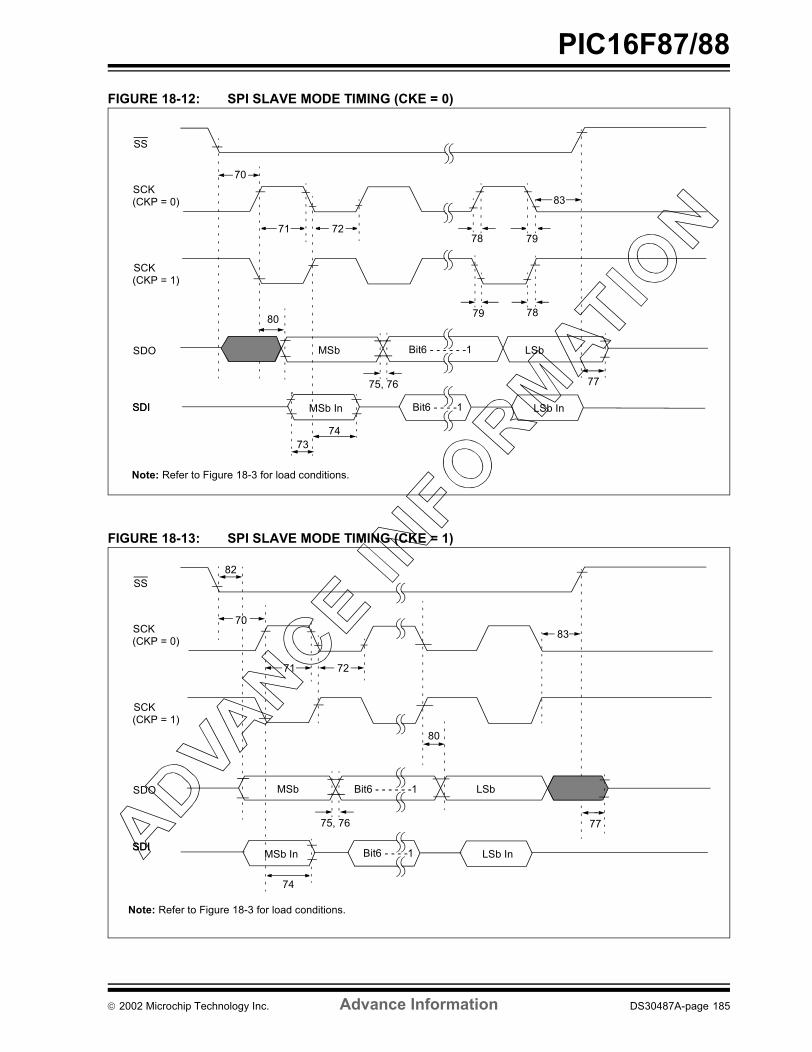
PIC16F87/88
FIGURE 18-12: SPI SLAVE MODE TIMING (CKE = 0)FIGURE 18-13: SPI SLAVE MODE TIMING (CKE = 1)
SS
SCK(CKP = 0)
SCK(CKP = 1)
SDO
SDI
70
71 72
7374
75, 76 77
787980
7978
SDI
MSb LSbBit6 - - - - - -1
MSb In Bit6 - - - -1 LSb In
83
Note: Refer to Figure 18-3 for load conditions.
SS
SCK(CKP = 0)
SCK(CKP = 1)
SDO
SDI
70
71 72
82
SDI
74
75, 76
MSb Bit6 - - - - - -1 LSb
77
MSb In Bit6 - - - -1 LSb In
80
83
Note: Refer to Figure 18-3 for load conditions.
2002 Microchip Technology Inc. Advance Information DS30487A-page 185

PIC16F87/88
TABLE 18-8: SPI MODE REQUIREMENTSFIGURE 18-14: I2C BUS START/STOP BITS TIMING
Param No. Symbol Characteristic Min Typ† Max Units Conditions
70* TssL2scH, TssL2scL
SS↓ to SCK↓ or SCK↑ input TCY — — ns
71* TscH SCK input high time (Slave mode) TCY + 20 — — ns72* TscL SCK input low time (Slave mode) TCY + 20 — — ns73* TdiV2scH,
TdiV2scLSetup time of SDI data input to SCK edge 100 — — ns
74* TscH2diL, TscL2diL
Hold time of SDI data input to SCK edge 100 — — ns
75* TdoR SDO data output rise time PIC16F87/88PIC16LF87/88
——
1025
2550
nsns
76* TdoF SDO data output fall time — 10 25 ns77* TssH2doZ SS↑ to SDO output hi-impedance 10 — 50 ns78* TscR SCK output rise time
(Master mode)PIC16F87/88PIC16LF87/88
——
1025
2550
nsns
79* TscF SCK output fall time (Master mode) — 10 25 ns80* TscH2doV,
TscL2doVSDO data output valid after SCK edge
PIC16F87/88PIC16LF87/88
——
——
50145
nsns
81* TdoV2scH,TdoV2scL
SDO data output setup to SCK edge TCY — — ns
82* TssL2doV SDO data output valid after SS↓ edge — — 50 ns83* TscH2ssH,
TscL2ssHSS ↑ after SCK edge 1.5 TCY + 40 — — ns
* These parameters are characterized but not tested.† Data in "Typ" column is at 5V, 25°C unless otherwise stated. These parameters are for design guidance only and are not
tested.
Note: Refer to Figure 18-3 for load conditions.
91
92
93SCL
SDA
STARTCondition
STOPCondition
90
DS30487A-page 186 Advance Information 2002 Microchip Technology Inc.

PIC16F87/88
TABLE 18-9: I2C BUS START/STOP BITS REQUIREMENTSFIGURE 18-15: I2C BUS DATA TIMING
ParamNo. Symbol Characteristic Min Typ Max Units Conditions
90* TSU:STA START condition 100 kHz mode 4700 — — ns Only relevant for Repeated START conditionSetup time 400 kHz mode 600 — —
91* THD:STA START condition 100 kHz mode 4000 — — ns After this period the first clock pulse is generatedHold time 400 kHz mode 600 — —
92* TSU:STO STOP condition 100 kHz mode 4700 — — nsSetup time 400 kHz mode 600 — —
93 THD:STO STOP condition 100 kHz mode 4000 — — nsHold time 400 kHz mode 600 — —
* These parameters are characterized but not tested.
Note: Refer to Figure 18-3 for load conditions.
90
91 92
100101
103
106 107
109 109110
102
SCL
SDAIn
SDAOut
2002 Microchip Technology Inc. Advance Information DS30487A-page 187

PIC16F87/88
TABLE 18-10: I2C BUS DATA REQUIREMENTSParam.No. Symbol Characteristic Min Max Units Conditions
100* THIGH Clock high time 100 kHz mode 4.0 — µs400 kHz mode 0.6 — µsSSP Module 1.5 TCY —
101* TLOW Clock low time 100 kHz mode 4.7 — µs400 kHz mode 1.3 — µsSSP Module 1.5 TCY —
102* TR SDA and SCL rise time
100 kHz mode — 1000 ns400 kHz mode 20 + 0.1 CB 300 ns CB is specified to be from
10 - 400 pF 103* TF SDA and SCL fall
time100 kHz mode — 300 ns400 kHz mode 20 + 0.1 CB 300 ns CB is specified to be from
10 - 400 pF 90* TSU:STA START condition
setup time100 kHz mode 4.7 — µs Only relevant for
Repeated START condition
400 kHz mode 0.6 — µs
91* THD:STA START condition hold time
100 kHz mode 4.0 — µs After this period, the first clock pulse is generated400 kHz mode 0.6 — µs
106* THD:DAT Data input hold time 100 kHz mode 0 — ns400 kHz mode 0 0.9 µs
107* TSU:DAT Data input setup time
100 kHz mode 250 — ns (Note 2)400 kHz mode 100 — ns
92* TSU:STO STOP condition setup time
100 kHz mode 4.7 — µs400 kHz mode 0.6 — µs
109* TAA Output valid from clock
100 kHz mode — 3500 ns (Note 1)400 kHz mode — — ns
110* TBUF Bus free time 100 kHz mode 4.7 — µs Time the bus must be free before a new transmission can start
400 kHz mode 1.3 — µs
CB Bus capacitive loading — 400 pF * These parameters are characterized but not tested.
Note 1: As a transmitter, the device must provide this internal minimum delay time to bridge the undefined region (min. 300 ns) of the falling edge of SCL to avoid unintended generation of START or STOP conditions.
2: A Fast mode (400 kHz) I2C bus device can be used in a Standard mode (100 kHz) I2C bus system, but the requirement TSU:DAT ≥ 250 ns must then be met. This will automatically be the case if the device does not stretch the LOW period of the SCL signal. If such a device does stretch the LOW period of the SCL signal, it must output the next data bit to the SDA line TR max. + TSU:DAT = 1000 + 250 = 1250 ns (according to the Standard mode I2C bus specification), before the SCL line is released.
DS30487A-page 188 Advance Information 2002 Microchip Technology Inc.

PIC16F87/88
FIGURE 18-16: USART SYNCHRONOUS TRANSMISSION (MASTER/SLAVE) TIMINGTABLE 18-11: USART SYNCHRONOUS TRANSMISSION REQUIREMENTS
FIGURE 18-17: USART SYNCHRONOUS RECEIVE (MASTER/SLAVE) TIMING
TABLE 18-12: USART SYNCHRONOUS RECEIVE REQUIREMENTS
ParamNo. Sym Characteristic Min Typ† Max Units Conditions
120 TckH2dtV SYNC XMIT (MASTER & SLAVE)Clock high to data out valid
PIC16F87/88— — 80 ns
PIC16LF87/88 — — 100 ns121 Tckrf Clock out rise time and fall time
(Master mode)PIC16F87/88 — — 45 nsPIC16LF87/88 — — 50 ns
122 Tdtrf Data out rise time and fall time PIC16F87/88 — — 45 nsPIC16LF87/88 — — 50 ns
† Data in “Typ” column is at 5V, 25°C unless otherwise stated. These parameters are for design guidance only and are not tested.
Parameter No. Sym Characteristic Min Typ† Max Units Conditions
125 TdtV2ckL SYNC RCV (MASTER & SLAVE)Data setup before CK↓ (DT setup time) 15 — — ns
126 TckL2dtl Data hold after CK↓ (DT hold time) 15 — — ns† Data in “Typ” column is at 5V, 25°C unless otherwise stated. These parameters are for design guidance only
and are not tested.
Note: Refer to Figure 18-3 for load conditions.
121121
122
RC6/TX/CK
RC7/RX/DTpin
pin
120
Note: Refer to Figure 18-3 for load conditions.
125
126
RC6/TX/CK
RC7/RX/DT
pin
pin
2002 Microchip Technology Inc. Advance Information DS30487A-page 189

PIC16F87/88
TABLE 18-13: A/D CONVERTER CHARACTERISTICS: PIC16F87/88 (INDUSTRIAL, EXTENDED)PIC16LF87/88 (INDUSTRIAL)
ParamNo. Sym Characteristic Min Typ† Max Units Conditions
A01 NR Resolution — — 10 bits bit VREF = VDD = 5.12V, VSS ≤ VAIN ≤ VREF
A03 EIL Integral linearity error — — < ± 1 LSb VREF = VDD = 5.12V, VSS ≤ VAIN ≤ VREF
A04 EDL Differential linearity error — — < ± 1 LSb VREF = VDD = 5.12V, VSS ≤ VAIN ≤ VREF
A06 EOFF Offset error — — < ± 2 LSb VREF = VDD = 5.12V, VSS ≤ VAIN ≤ VREF
A07 EGN Gain error — — < ± 1 LSb VREF = VDD = 5.12V, VSS ≤ VAIN ≤ VREF
A10 — Monotonicity(3) — guaranteed — — VSS ≤ VAIN ≤ VREF
A20 VREF Reference Voltage 2.52.2
——
VDD + 0.3VDD + 0.3
VV
-40°C to +85°C0°C to +85°C
A21 VREF+ Reference voltage high AVDD – 2.5V AVDD + 0.3V VA22 VREF- Reference voltage low AVSS – 0.3V VREF+ – 2.0V VA25 VAIN Analog input voltage VSS – 0.3V — VREF + 0.3V VA30 ZAIN Recommended impedance of
analog voltage source— — 2.5 kΩ See (Note 4)
A50 IREF VREF input current(2) —
—
—
—
5
500
µA
µA
During VAIN acquisition.Based on differential of VHOLD to VAIN to charge CHOLD, see Section 12.1.During A/D Conversion cycle.
* These parameters are characterized but not tested.† Data in "Typ" column is at 5V, 25°C unless otherwise stated. These parameters are for design guidance only and are
not tested.Note 1: When A/D is off, it will not consume any current other than minor leakage current.
The power-down current spec includes any such leakage from the A/D module.2: VREF current is from RA3 pin or VDD pin, whichever is selected as reference input.3: The A/D conversion result never decreases with an increase in the input voltage, and has no missing codes.4: The maximum allowed impedance for analog voltage source is 10 kΩ. This requires higher acquisition times.
DS30487A-page 190 Advance Information 2002 Microchip Technology Inc.

PIC16F87/88
FIGURE 18-18: A/D CONVERSION TIMINGTABLE 18-14: A/D CONVERSION REQUIREMENTS
131
130
132
BSF ADCON0, GO
Q4
A/D CLK
A/D DATA
ADRES
ADIF
GO
SAMPLE
OLD_DATA
SAMPLING STOPPED
DONE
NEW_DATA
(TOSC/2)(1)
9 8 7 2 1 0
Note 1: If the A/D clock source is selected as RC, a time of TCY is added before the A/D clock starts. This allows theSLEEP instruction to be executed.
1 TCY
. . . . . .
Param No. Sym Characteristic Min Typ† Max Units Conditions
130 TAD A/D clock period PIC16F87/88 1.6 — — µs TOSC based, VREF ≥ 3.0VPIC16LF87/88 3.0 — — µs TOSC based, VREF ≥ 2.0VPIC16F87/88 2.0 4.0 6.0 µs A/D RC modePIC16LF87/88 3.0 6.0 9.0 µs A/D RC mode
131 TCNV Conversion time (not including S/H time) (Note 1)
— 12 TAD
132 TACQ Acquisition time (Note 2)10*
40—
——
µsµs The minimum time is the
amplifier settling time. This may be used if the "new" input voltage has not changed by more than 1 LSb (i.e., 20.0 mV @ 5.12V) from the last sampled voltage (as stated on CHOLD).
134 TGO Q4 to A/D clock start — TOSC/2 — — If the A/D clock source is selected as RC, a time of TCY is added before the A/D clock starts. This allows the SLEEP instruction to be executed.
* These parameters are characterized but not tested.† Data in "Typ" column is at 5V, 25°C unless otherwise stated. These parameters are for design guidance only and are
not tested.§ This specification ensured by design.
Note 1: ADRES register may be read on the following TCY cycle.2: See Section 12.1 for minimum conditions.
2002 Microchip Technology Inc. Advance Information DS30487A-page 191

PIC16F87/88
NOTES:DS30487A-page 192 Advance Information 2002 Microchip Technology Inc.

PIC16F87/88
19.0 DC AND AC CHARACTERISTICS GRAPHS AND TABLES
No Graphs and Tables are available at this time.
2002 Microchip Technology Inc. Advance Information DS30487A-page 193

PIC16F87/88
NOTES:DS30487A-page 194 Advance Information 2002 Microchip Technology Inc.

PIC16F87/88
20.0 PACKAGING INFORMATION
20.1 Package Marking Information
18-Lead PDIP
XXXXXXXXXXXXXXXXXXXXXXXXXXXXXXXXXX
YYWWNNN
Example
PIC16F87/88-I/P
0210017
YYWWNNNXXXXXXXXXXXXXXXXXXXXXXXX
18-Lead SOIC
XXXXXXXXXXXX
0210017
04/SO
Example
PIC16F87/88-
YYWWNNNXXXXXXXXXXXXXXXXXXXXXX
20-Lead SSOP
021001720/SSPIC16F87-
Example
Legend: XX...X Customer specific information*Y Year code (last digit of calendar year)YY Year code (last 2 digits of calendar year)WW Week code (week of January 1 is week ‘01’)NNN Alphanumeric traceability code
Note: In the event the full Microchip part number cannot be marked on one line, it willbe carried over to the next line thus limiting the number of available charactersfor customer specific information.
* Standard PICmicro device marking consists of Microchip part number, year code, week code, andtraceability code. For PICmicro device marking beyond this, certain price adders apply. Please checkwith your Microchip Sales Office. For QTP devices, any special marking adders are included in QTPprice.
28-Lead QFN Example
XXXXXXXXXXXXXXXXYYWWNNN
PIC16F87-I/ML0210017
2002 Microchip Technology Inc. Advance Information DS30487A-page 195

PIC16F87/88
18-Lead Plastic Dual In-line (P) – 300 mil (PDIP)1510515105βMold Draft Angle Bottom1510515105αMold Draft Angle Top
10.929.407.87.430.370.310eBOverall Row Spacing §0.560.460.36.022.018.014BLower Lead Width1.781.461.14.070.058.045B1Upper Lead Width0.380.290.20.015.012.008cLead Thickness3.433.303.18.135.130.125LTip to Seating Plane
22.9922.8022.61.905.898.890DOverall Length6.606.356.10.260.250.240E1Molded Package Width8.267.947.62.325.313.300EShoulder to Shoulder Width
0.38.015A1Base to Seating Plane3.683.302.92.145.130.115A2Molded Package Thickness4.323.943.56.170.155.140ATop to Seating Plane
2.54.100pPitch1818nNumber of Pins
MAXNOMMINMAXNOMMINDimension LimitsMILLIMETERSINCHES*Units
1
2
D
n
E1
c
eB
β
E
α
p
A2
L
B1
B
A
A1
* Controlling Parameter
Notes:Dimensions D and E1 do not include mold flash or protrusions. Mold flash or protrusions shall not exceed .010” (0.254mm) per side.JEDEC Equivalent: MS-001Drawing No. C04-007
§ Significant Characteristic
DS30487A-page 196 Advance Information 2002 Microchip Technology Inc.

PIC16F87/88
18-Lead Plastic Small Outline (SO) – Wide, 300 mil (SOIC)Foot Angle φ 0 4 8 0 4 8
1512015120βMold Draft Angle Bottom1512015120αMold Draft Angle Top
0.510.420.36.020.017.014BLead Width0.300.270.23.012.011.009cLead Thickness
1.270.840.41.050.033.016LFoot Length0.740.500.25.029.020.010hChamfer Distance
11.7311.5311.33.462.454.446DOverall Length7.597.497.39.299.295.291E1Molded Package Width
10.6710.3410.01.420.407.394EOverall Width0.300.200.10.012.008.004A1Standoff §2.392.312.24.094.091.088A2Molded Package Thickness2.642.502.36.104.099.093AOverall Height
1.27.050pPitch1818nNumber of Pins
MAXNOMMINMAXNOMMINDimension LimitsMILLIMETERSINCHES*Units
Lβ
c
φ
h
45°
1
2
D
p
nB
E1
E
α
A2
A1
A
* Controlling Parameter
Notes:Dimensions D and E1 do not include mold flash or protrusions. Mold flash or protrusions shall not exceed .010” (0.254mm) per side.JEDEC Equivalent: MS-013Drawing No. C04-051
§ Significant Characteristic
2002 Microchip Technology Inc. Advance Information DS30487A-page 197

PIC16F87/88
20-Lead Plastic Shrink Small Outline (SS) – 209 mil, 5.30 mm (SSOP)10501050βMold Draft Angle Bottom10501050αMold Draft Angle Top
0.380.320.25.015.013.010BLead Width203.20101.600.00840φFoot Angle
0.250.180.10.010.007.004cLead Thickness0.940.750.56.037.030.022LFoot Length7.347.207.06.289.284.278DOverall Length5.385.255.11.212.207.201E1Molded Package Width8.187.857.59.322.309.299EOverall Width0.250.150.05.010.006.002A1Standoff §1.831.731.63.072.068.064A2Molded Package Thickness1.981.851.73.078.073.068AOverall Height
0.65.026pPitch2020nNumber of Pins
MAXNOMMINMAXNOMMINDimension LimitsMILLIMETERSINCHES*Units
21
D
p
n
B
E
E1
L
c
β
φ
α
A2A
A1
* Controlling Parameter
Notes:Dimensions D and E1 do not include mold flash or protrusions. Mold flash or protrusions shall not exceed .010” (0.254mm) per side.JEDEC Equivalent: MO-150Drawing No. C04-072
§ Significant Characteristic
DS30487A-page 198 Advance Information 2002 Microchip Technology Inc.

PIC16F87/88
28-Lead Plastic Quad Flat No Lead Package (ML) 6x6 mm Body (QFN)Lead Width
*Controlling ParameterNotes:
Mold Draft Angle Top
B
α
.009
12
.011 .014 0.23
12
0.28 0.35
D
PitchNumber of Pins
Overall Width
Standoff
Molded Package LengthOverall Length
Molded Package Width
Molded Package ThicknessOverall Height
MAXUnits
Dimension Limits
A2A1
E1
DD1
E
np
A.026
.236 BSC
.000
.226 BSC
INCHES
.026 BSC
MIN28
NOM MAX
0.65.031.002 0.00
6.00 BSC5.75 BSC
MILLIMETERS*
.039
MIN28
0.65 BSC
NOM
0.800.05
1.00
E
E1
n
1
2
D1
AA2
EXPOSEDMETAL
PADS
BOTTOM VIEW
.008 REF.Base Thickness A3 0.20 REF.
TOP VIEW
0.85.033
.0004 0.01
.236 BSC
.226 BSC6.00 BSC5.75 BSC
Q
L
Lead LengthTie Bar Width
L .020 .024 .030 0.50 0.60 0.75R .005 .007 .010 0.13 0.17 0.23
Tie Bar Length Q .012 .016 .026 0.30 0.40 0.65Chamfer CH .009 .017 .024 0.24 0.42 0.60
R
p
A1
A3
α
CH x 45
B
D2
E2
E2
D2
Exposed Pad Width
Exposed Pad Length .140 .146 .152 3.55 3.70 3.85
.140 .146 .152 3.55 3.70 3.85
Dimensions D and E1 do not include mold flash or protrusions. Mold flash or protrusions shall not exceed .010” (0.254mm) per side.JEDEC equivalent: M0-220Drawing No. C04-114
2002 Microchip Technology Inc. Advance Information DS30487A-page 199

PIC16F87/88
28-Lead Plastic Quad Flat No Lead Package (ML) 6x6 mm Body (QFN)Land Pattern and Solder MaskPad Width
*Controlling Parameter
Drawing No. C04-2114
B .009 .011 .014 0.23 0.28 0.35Pitch
MAXUnits
Dimension Limitsp
INCHES
.026 BSCMIN NOM MAX
MILLIMETERS*MIN
0.65 BSCNOM
Pad LengthPad to Solder Mask
L .020 .024 .030 0.50 0.60 0.75M .005 .006 0.13 0.15
L
p
B
PACKAGEEDGE
SOLDERMASK
M
M
DS30487A-page 200 Advance Information 2002 Microchip Technology Inc.

PIC16F87/88
APPENDIX A: REVISION HISTORY
APPENDIX B: DEVICE DIFFERENCESThe differences between the devices in this data sheet are listed in Table B-1.
TABLE B-1: DIFFERENCES BETWEEN THE PIC16F87 AND PIC16F88
Version Date Revision Description
A November 2002 This is a new data sheet.
Features PIC16F87 PIC16F88
Analog-to-Digital Converter N/A 10-bit, 7-channel
2002 Microchip Technology Inc. Advance Information DS30487A-page 201

PIC16F87/88
NOTES:DS30487A-page 202 Advance Information 2002 Microchip Technology Inc.

PIC16F87/88
INDEXAA/D
Acquisition Requirements ........................................ 119ADIF Bit .................................................................... 118Analog-to-Digital Converter ...................................... 115Associated Registers ............................................... 122Calculating Acquisition Time .................................... 119Configuring Analog Port Pins ................................... 120Configuring the Interrupt .......................................... 118Configuring the Module ............................................ 118Conversion Clock ..................................................... 120Conversions ............................................................. 121Converter Characteristics ........................................ 190Delays ...................................................................... 119Effects of a RESET .................................................. 122GO/DONE Bit ........................................................... 118Internal Sampling Switch (Rss) Impedance ............. 119Operation During SLEEP ......................................... 122Result Registers ....................................................... 121Source Impedance ................................................... 119Time Delays ............................................................. 119Using the CCP Trigger ............................................. 122
Absolute Maximum Ratings ............................................. 165ACK .................................................................................... 95ADCON0 Register ...................................................... 14, 115ADCON1 Register ...................................................... 15, 115Addressable Universal Synchronous Asynchronous
Receiver Transmitter. See USARTADRESH Register ...................................................... 14, 115ADRESH, ADRESL Register Pair .................................... 118ADRESL Register ...................................................... 15, 115ANSEL Register ......................................................... 15, 115Application Notes
AN556 (Implementing a Table Read) ........................ 25AN578 (Use of the SSP Module in the
I2C Multi-Master Environment) ........................... 89AN607 (Power-up Trouble Shooting) ....................... 135
AssemblerMPASM Assembler .................................................. 159
Asynchronous ReceptionAssociated Registers ....................................... 107, 109
Asynchronous TransmissionAssociated Registers ............................................... 105
BBaud Rate Generator
Associated Registers ............................................... 101BF Bit ................................................................................. 94Block Diagrams
A/D ........................................................................... 118Analog Input Model .......................................... 119, 127Capture Mode Operation ........................................... 84Comparator I/O Operating Modes ............................ 124Comparator Output .................................................. 126Comparator Voltage Reference ............................... 130Compare Mode Operation ......................................... 85Fail-Safe Clock Monitor ............................................ 145In-Circuit Serial Programming Connections ............. 148Interrupt Logic .......................................................... 140On-Chip Reset Circuit .............................................. 134PIC16F87 ..................................................................... 6PIC16F88 ..................................................................... 7
PWM .......................................................................... 86RA0/AN0:RA1/AN1 Pins ............................................ 54RA2/AN2/CVREF/VREF- Pin ....................................... 55RA3/AN3/VREF+/C1OUT Pin ..................................... 55RA4/T0CKI/C2OUT Pin ............................................. 56RA5/MCLR/VPP Pin ................................................... 56RA6/OSC2/CLKO Pin ................................................ 57RA7/OSC1/CLKI Pin .................................................. 58RB0 Pin ..................................................................... 61RB1 Pin ..................................................................... 62RB2 Pin ..................................................................... 63RB3 Pin ..................................................................... 64RB4 Pin ..................................................................... 65RB5 Pin ..................................................................... 66RB6 Pin ..................................................................... 67RB7 Pin ..................................................................... 68Recommended MCLR Circuit .................................. 135SSP in I2C Mode ........................................................ 94SSP in SPI Mode ....................................................... 92System Clock ............................................................. 40Timer0/WDT Prescaler .............................................. 69Timer1 ....................................................................... 75Timer2 ....................................................................... 81USART Receive ................................................106, 108USART Transmit ...................................................... 104Watchdog Timer (WDT) ........................................... 142
BOR. See Brown-out ResetBRGH bit .......................................................................... 101Brown-out Reset (BOR) ............................ 131, 134, 135, 137
BOR Status (BOR Bit) ............................................... 24
CCapture/Compare/PWM (CCP) ......................................... 83
Capture Mode ............................................................ 84Capture, Compare and Timer1
Associated Registers ......................................... 85CCP Pin Configuration ............................................... 85CCP Prescaler ........................................................... 84CCP Timer Resources ............................................... 83CCP1IF ...................................................................... 84CCPR1 ...................................................................... 84CCPR1H:CCPR1L ..................................................... 84Compare
Mode .................................................................. 85Special Event Trigger and
A/D Conversions ........................................ 85Special Trigger Output of CCP1 ........................ 85
PWM and Timer2Associated Registers ......................................... 87
PWM Mode ................................................................ 86PWM, Example Frequencies/Resolutions ................. 87Software Interrupt Mode ............................................ 85Timer1 Mode Selection .............................................. 85
CCP1CON Register ........................................................... 14CCP1M0 Bit ....................................................................... 83CCP1M1 Bit ....................................................................... 83CCP1M2 Bit ....................................................................... 83CCP1M3 Bit ....................................................................... 83CCP1X Bit .......................................................................... 83CCP1Y Bit .......................................................................... 83CCPR1H Register .........................................................14, 83CCPR1L Register .........................................................14, 83
2002 Microchip Technology Inc. Advance Information DS30487A-page 203

PIC16F87/88
Clock Sources .................................................................... 39Selection Using OSCCON Register ........................... 39Clock Switching .................................................................. 43
Transition and the Watchdog ..................................... 43Transition Delays ....................................................... 43
CMCON Register ............................................................... 15Code Examples
Call of a Subroutine in Page 1 from Page 0 ............... 25Changing Between Capture Prescalers ..................... 84Changing Prescaler Assignment from WDT
to Timer0 ............................................................ 71Erasing a FLASH Program Memory Row .................. 31Implementing a Real-Time Clock Using a
Timer1 Interrupt Service .................................... 79Initializing PORTA ...................................................... 53Reading a 16-bit Free-Running Timer ........................ 76Reading Data EEPROM ............................................. 29Reading FLASH Program Memory ............................ 30Saving STATUS and W Registers in RAM ............... 141Writing a 16-bit Free-Running Timer .......................... 76Writing to Data EEPROM ........................................... 29Writing to FLASH Program Memory ........................... 33
Code Protection ....................................................... 131, 148Comparator Module ......................................................... 123
Analog Input Connection Considerations ................. 127Associated Registers ............................................... 128Configuration ............................................................ 124Effects of RESET ..................................................... 127Interrupts .................................................................. 126Operation ................................................................. 125Operation During SLEEP ......................................... 127Outputs ..................................................................... 125Reference ................................................................. 125Response Time ........................................................ 125
Comparator Specifications ............................................... 177Comparator Voltage Reference ....................................... 129
Associated Registers ............................................... 130Computed GOTO ............................................................... 25Configuration Bits ............................................................. 131Crystal and Ceramic Resonators ....................................... 35CVRCON Register ............................................................. 15
DData EEPROM Memory ..................................................... 27
Associated Registers ................................................. 34EEADR Register ........................................................ 27EEADRH Register ...................................................... 27EECON1 Register ...................................................... 27EECON2 Register ...................................................... 27EEDATA Register ...................................................... 27EEDATH Register ...................................................... 27Operation During Code Protect .................................. 34Protection Against Spurious Writes ............................ 34Reading ...................................................................... 29Write Complete Flag (EEIF Bit) .................................. 27Writing ........................................................................ 29
Data MemorySpecial Function Registers ........................................ 14
DC and AC CharacteristicsGraphs and Tables ................................................... 193
DC CharacteristicsInternal RC Accuracy ............................................... 174PIC16F87/88, PIC16LF87/88 ................................... 175Power-down and Supply Current ............................. 168Supply Voltage ......................................................... 167
Development Support ...................................................... 159Device Differences ........................................................... 201Device Overview .................................................................. 5Direct Addressing ............................................................... 26
EEEADR Register ...........................................................16, 27EEADRH Register .........................................................16, 27EECON1 Register .........................................................16, 27EECON2 Register .........................................................16, 27EEDATA Register .........................................................16, 27EEDATH Register .........................................................16, 27Electrical Characteristics .................................................. 165Endurance ........................................................................... 1Errata ................................................................................... 4Exiting SLEEP with an Interrupt ......................................... 51External Clock Input ........................................................... 36External Clock Input (RA4/T0CKI). See Timer0External Interrupt Input (RB0/INT). See Interrupt SourcesExternal Reference Signal ............................................... 125
FFail-Safe Clock Monitor .............................................131, 145FLASH Program Memory ................................................... 27
Associated Registers ................................................. 34EEADR Register ........................................................ 27EEADRH Register ..................................................... 27EECON1 Register ...................................................... 27EECON2 Register ...................................................... 27EEDATA Register ...................................................... 27EEDATH Register ...................................................... 27Erasing ....................................................................... 30Reading ..................................................................... 30Writing ........................................................................ 32
FSR Register ................................................................14, 15
II/O Ports ............................................................................. 53
PORTA ...................................................................... 53PORTB ...................................................................... 59TRISB Register .......................................................... 59
I2CAddressing ................................................................. 95Associated Registers ................................................. 97Master Mode .............................................................. 97Mode .......................................................................... 94Mode Selection .......................................................... 94Multi-Master Mode ..................................................... 97Reception ................................................................... 95SCL and SDA pins ..................................................... 94Slave Mode ................................................................ 94Transmission ............................................................. 95
ICEPIC In-Circuit Emulator .............................................. 160ID Locations ..............................................................131, 148In-Circuit Debugger .......................................................... 148In-Circuit Serial Programming .......................................... 131In-Circuit Serial Programming (ICSP) .............................. 148INDF Register ...............................................................14, 15Indirect Addressing ............................................................ 26
DS30487A-page 204 Advance Information 2002 Microchip Technology Inc.

PIC16F87/88
Instruction Set .................................................................. 151ADDLW .................................................................... 153ADDWF .................................................................... 153ANDLW .................................................................... 153ANDWF .................................................................... 153BCF .......................................................................... 153BSF .......................................................................... 153BTFSC ..................................................................... 154BTFSS ..................................................................... 154CALL ........................................................................ 154CLRF ........................................................................ 154CLRW ...................................................................... 154CLRWDT .................................................................. 154COMF ...................................................................... 155DECF ....................................................................... 155DECFSZ ................................................................... 155Descriptions ............................................................. 153Format ...................................................................... 151GOTO ...................................................................... 155INCF ......................................................................... 155INCFSZ .................................................................... 155IORLW ..................................................................... 156IORWF ..................................................................... 156MOVF ....................................................................... 156MOVLW ................................................................... 156MOVWF ................................................................... 156NOP ......................................................................... 156Read-Modify-Write Operations ................................ 151RETFIE .................................................................... 157RETLW .................................................................... 157RETURN .................................................................. 157RLF .......................................................................... 157RRF .......................................................................... 157SLEEP ..................................................................... 157SUBLW .................................................................... 158SUBWF .................................................................... 158Summary Table ........................................................ 152SWAPF .................................................................... 158XORLW .................................................................... 158XORWF .................................................................... 158
INT Interrupt (RB0/INT). See Interrupt SourcesINTCON Register
GIE Bit ........................................................................ 19INTE Bit ...................................................................... 19INTF Bit ...................................................................... 19PEIE Bit ...................................................................... 19RBIE Bit ..................................................................... 19RBIF Bit ...................................................................... 19TMR0IE Bit ................................................................. 19
Internal Oscillator Block ..................................................... 37INTRC Modes ............................................................ 38
Internal Reference Signal ................................................. 125Interrupt Sources ...................................................... 131, 140
RB0/INT Pin, External .............................................. 141TMR0 Overflow ........................................................ 141USART Receive/Transmit Complete ......................... 99
InterruptsRB7:RB4 Port Change ............................................... 59
Interrupts, Context Saving During .................................... 141
Interrupts, Enable BitsA/D Converter Interrupt Enable (ADIE Bit) ................ 20CCP1 Interrupt Enable (CCP1IE Bit) ......................... 20Comparator Interrupt Enable (CMIE Bit) .................... 22EEPROM Write Operation Interrupt
Enable (EEIE Bit) ............................................... 22Global Interrupt Enable (GIE Bit) ........................19, 140Interrupt-on-Change (RB7:RB4) Enable
(RBIE Bit) ......................................................... 141Oscillator Fail Interrupt Enable (OSFIE Bit) ............... 22Peripheral Interrupt Enable (PEIE Bit) ....................... 19Port Change Interrupt Enable (RBIE Bit) ................... 19RB0/INT Enable (INTE Bit) ........................................ 19Synchronous Serial Port (SSP) Interrupt
Enable (SSPIE Bit) ............................................ 20TMR0 Overflow Enable (TMR0IE Bit) ........................ 19TMR1 Overflow Interrupt Enable (TMR1IE Bit) ......... 20TMR2 to PR2 Match Interrupt Enable
(TMR2IE Bit) ...................................................... 20USART Interrupt Enable (RCIE Bit) ........................... 20USART Transmit Interrupt Enable (TXIE Bit) ............ 20
Interrupts, Flag BitsA/D Converter Interrupt Flag (ADIF Bit) ..................... 21CCP1 Interrupt Flag (CCP1IF Bit) ............................. 21Comparator Interrupt Flag (CMIF Bit) ........................ 23EEPROM Write Operation Interrupt
Flag (EEIF Bit) ................................................... 23Interrupt-on-Change (RB7:RB4) Flag
(RBIF Bit) ....................................................19, 141Oscillator Fail Interrupt Flag (OSFIF Bit) ................... 23RB0/INT Flag (INTF Bit) ............................................ 19Synchronous Serial Port (SSP) Interrupt
Flag (SSPIF Bit) ................................................. 21TMR0 Overflow Flag (TMR0IF Bit) .......................... 141TMR1 Overflow Interrupt Flag (TMR1IF Bit) .............. 21TMR2 to PR2 Interrupt Flag (TMR2IF Bit) ................. 21USART Receive Interrupt Flag (RCIF Bit) ................. 21USART Transmit Interrupt Flag (TXIF Bit) ................. 21
INTRC ModesAdjustment ................................................................. 38
KKEELOQ Evaluation and Programming Tools ................... 162
LLoading of PC .................................................................... 25Low Voltage ICSP Programming ..................................... 149
MMaster Clear (MCLR)
MCLR Reset, Normal Operation .......................134, 137MCLR Reset, SLEEP ........................................134, 137Operation and ESD Protection ................................ 135
Memory Organization ........................................................ 11Data Memory ............................................................. 11Program Memory ....................................................... 11
MPLAB C17 and MPLAB C18 C Compilers .................... 159MPLAB ICD In-Circuit Debugger ..................................... 161MPLAB ICE High Performance Universal
In-Circuit Emulator with MPLAB IDE ....................... 160MPLAB Integrated Development
Environment Software ............................................. 159MPLINK Object Linker/MPLIB Object Librarian ............... 160
2002 Microchip Technology Inc. Advance Information DS30487A-page 205

PIC16F87/88
OOpcode Field Descriptions ............................................... 151OPTION RegisterINTEDG Bit ................................................................ 18PS2:PS0 Bits .............................................................. 18PSA Bit ....................................................................... 18RBPU Bit .................................................................... 18T0CS Bit ..................................................................... 18T0SE Bit ..................................................................... 18
OSCCON Register ............................................................. 15Oscillator Configuration ...................................................... 35
ECIO .......................................................................... 35EXTRC ..................................................................... 136HS ...................................................................... 35, 136INTIO1 ........................................................................ 35INTIO2 ........................................................................ 35INTRC ...................................................................... 136LP ....................................................................... 35, 136RC ........................................................................ 35, 37RCIO .......................................................................... 35XT ....................................................................... 35, 136
Oscillator Control RegisterModifying IRCF Bits ................................................... 40
Clock Transition Sequence ................................ 40Oscillator Delay upon Power-up and Wake-up .................. 42Oscillator Start-up Timer (OST) ............................... 131, 135Oscillator Switching ............................................................ 39OSCTUNE Register ........................................................... 15
PPackaging Information ..................................................... 195
Marking .................................................................... 195Paging, Program Memory .................................................. 25PCL Register .......................................................... 14, 15, 25PCLATH Register ................................................... 14, 15, 25PCON Register .......................................................... 15, 136
BOR Bit ...................................................................... 24POR Bit ...................................................................... 24
PICDEM 1 Low Cost PICmicro Demonstration Board ............................................... 161
PICDEM 17 Demonstration Board ................................... 162PICDEM 2 Low Cost PIC16CXX
Demonstration Board ............................................... 161PICDEM 3 Low Cost PIC16CXXX
Demonstration Board ............................................... 162PICSTART Plus Entry Level
Development Programmer ....................................... 161PIE1 Register ..................................................................... 15
ADIE Bit ...................................................................... 20CCP1IE Bit ................................................................. 20RCIE Bit ..................................................................... 20SSPIE Bit ................................................................... 20TMR1IE Bit ................................................................. 20TMR2IE Bit ................................................................. 20TXIE Bit ...................................................................... 20
PIE2 Register ..................................................................... 15CMIE Bit ..................................................................... 22EEIE Bit ...................................................................... 22OSFIE Bit ................................................................... 22
Pinout DescriptionsPIC16F87/88 ................................................................ 8
PIR1 Register .................................................................... 14ADIF Bit ..................................................................... 21CCP1IF Bit ................................................................. 21RCIF Bit ..................................................................... 21SSPIF Bit ................................................................... 21TMR1IF Bit ................................................................. 21TMR2IF Bit ................................................................. 21TXIF Bit ...................................................................... 21
PIR2 Register .................................................................... 14CMIF Bit ..................................................................... 23EEIF Bit ...................................................................... 23OSFIF Bit ................................................................... 23
POP ................................................................................... 25POR. See Power-on ResetPORTA ................................................................................ 8
Associated Register Summary .................................. 54PORTA Register ........................................................ 14
PORTB ................................................................................ 9Associated Register Summary .................................. 60PORTB Register ........................................................ 14Pull-up Enable (RBPU Bit) ......................................... 18RB0/INT Edge Select (INTEDG Bit) .......................... 18RB0/INT Pin, External .............................................. 141RB2/SDO/RX/DT Pin ........................................100, 101RB5/SS/TX/CK Pin .................................................. 100RB7:RB4 Interrupt-on-Change ................................ 141RB7:RB4 Interrupt-on-Change
Enable (RBIE Bit) ............................................. 141RB7:RB4 Interrupt-on-Change Flag
(RBIF Bit) ....................................................19, 141TRISB Register .....................................................16, 99
PORTB Register ................................................................ 16Postscaler, WDT
Assignment (PSA Bit) ................................................ 18Rate Select (PS2:PS0 Bits) ....................................... 18
Power Managed Modes ..................................................... 44RC_RUN .................................................................... 44SEC_RUN .................................................................. 45SEC_RUN/RC_RUN to Primary Clock Source .......... 46
Power-down Mode. See SLEEPPower-on Reset (POR) ............................. 131, 134, 135, 137
POR Status (POR Bit) ............................................... 24Power Control (PCON) Register .............................. 136Power-down (PD Bit) ............................................... 134Time-out (TO Bit) ................................................17, 134
Power-up Timer (PWRT) ..........................................131, 135PR2 Register ................................................................15, 81Prescaler, Timer0
Assignment (PSA Bit) ................................................ 18Rate Select (PS2:PS0 Bits) ....................................... 18
PRO MATE II Universal Device Programmer .................. 161Program Counter
RESET Conditions ................................................... 137Program Memory
Interrupt Vector .......................................................... 11Map and Stack
PIC16F87/88 ..................................................... 11Paging ........................................................................ 25RESET Vector ........................................................... 11
Program Verification ........................................................ 148PUSH ................................................................................. 25
DS30487A-page 206 Advance Information 2002 Microchip Technology Inc.

PIC16F87/88
RR/W Bit ............................................................................... 95RA0/AN0 Pin ........................................................................ 8RA1/AN1 Pin ........................................................................ 8RA2/AN2/CVREF/VREF- Pin .................................................. 8RA3/AN3/VREF+/C1OUT Pin ................................................ 8RA4/AN4/T0CKI/C2OUT Pin ................................................ 8RA5/MCLR/VPP Pin .............................................................. 8RA6/OSC2/CLKO Pin .......................................................... 8RA7/OSC1/CLKI Pin ............................................................ 8RB0/INT/CCP1 Pin ............................................................... 9RB1/SDI/SDA Pin ................................................................. 9RB2/SDO/RX/DT Pin ........................................................... 9RB3/CCP1/PGM Pin ............................................................ 9RB4/SCK/SCL Pin ................................................................ 9RB5/SS/TX/CK Pin ............................................................... 9RB6/T1OSO/T1CKI/PGC/AN5 Pin ....................................... 9RB7/T1OSI/PGD/AN6 Pin .................................................... 9RBIF Bit .............................................................................. 59RCIO Oscillator .................................................................. 37RCREG Register ................................................................ 14RCSTA Register ................................................................. 14ADDEN Bit ............................................................... 100CREN Bit .................................................................. 100FERR Bit .................................................................. 100RX9 Bit ..................................................................... 100RX9D Bit .................................................................. 100SPEN Bit ............................................................ 99, 100SREN Bit .................................................................. 100
Receive Overflow Indicator Bit, SSPOV ............................. 91Register File ....................................................................... 12Register File Map
PIC16F87 ................................................................... 12PIC16F88 ................................................................... 13
RegistersADCON0 (A/D Control 0) ......................................... 116ADCON1 (A/D Control 1) ......................................... 117ANSEL (Analog Select) ............................................ 115CCP1CON (Capture/Compare/PWM
Control 1) ........................................................... 83CMCON (Comparator Control) ................................ 123CVRCON (Comparator Voltage Reference
Control) ............................................................ 129EECON1 (Data EEPROM Access Control 1) ............. 28Initialization Conditions (table) ......................... 137–138INTCON (Interrupt Control) ........................................ 19OPTION ..................................................................... 18OPTION_REG ........................................................... 70OSCCON (Oscillator Control) .................................... 41OSCTUNE (Oscillator Tuning) ................................... 38PCON (Power Control) .............................................. 24PIE1 (Peripheral Interrupt Enable 1) .......................... 20PIE2 (Peripheral Interrupt Enable 2) .......................... 22PIR1 (Peripheral Interrupt Status 1) ........................... 21PIR2 (Peripheral Interrupt Status 2) ........................... 23RCSTA (Receive Status and Control) ...................... 100Special Function, Summary ....................................... 14SSPCON (Synchronous Serial Port Control 1) .......... 91SSPSTAT (Synchronous Serial Port Status) ............. 90STATUS ..................................................................... 17T1CON (Timer1 Control) ............................................ 74T2CON (Timer2 Control) ............................................ 82TXSTA (Transmit Status and Control) ....................... 99
RESET ......................................................................131, 134Brown-out Reset (BOR). See Brown-out Reset (BOR)MCLR RESET. See MCLRPower-on Reset (POR). See Power-on Reset (POR)RESET Conditions for All Registers ........................ 137RESET Conditions for PCON Register .................... 137RESET Conditions for Program Counter ................. 137RESET Conditions for STATUS Register ................ 137WDT Reset. See Watchdog Timer (WDT)
Revision History ............................................................... 201RP0 Bit ............................................................................... 11RP1 Bit ............................................................................... 11
SSales and Support ........................................................... 213SCI. See USARTSCL .................................................................................... 94Serial Communication Interface. See USARTSlave Mode
SCL ............................................................................ 94SDA ........................................................................... 94
SLEEP ..............................................................131, 134, 146Software Simulator (MPLAB SIM) ................................... 160SPBRG Register ................................................................ 15Special Event Trigger ...................................................... 122Special Features of the CPU ........................................... 131Special Function Registers ................................................ 14Special Function Registers (SFRs) .................................... 14SPI
Associated Registers ................................................. 92Serial Clock ................................................................ 89Serial Data In ............................................................. 89Serial Data Out .......................................................... 89Slave Select ............................................................... 89
SSPACK ........................................................................... 94I2C
I2C Operation ..................................................... 94SSPADD Register .............................................................. 15SSPBUF Register .............................................................. 14SSPCON Register ............................................................. 14SSPOV .............................................................................. 91SSPOV Bit ......................................................................... 94SSPSTAT Register ............................................................ 15Stack .................................................................................. 25
Overflows ................................................................... 25Underflow .................................................................. 25
STATUS RegisterC Bit ........................................................................... 17DC Bit ........................................................................ 17IRP Bit ....................................................................... 17PD Bit .................................................................17, 134RP Bit ........................................................................ 17TO Bit .................................................................17, 134Z Bit ........................................................................... 17
Synchronous Master ReceptionAssociated Registers ............................................... 112
Synchronous Master TransmissionAssociated Registers ............................................... 111
Synchronous Serial Port (SSP) ......................................... 89Overview .................................................................... 89SPI Mode ................................................................... 89
Synchronous Slave ReceptionAssociated Registers ............................................... 114
Synchronous Slave TransmissionAssociated Registers ............................................... 114
2002 Microchip Technology Inc. Advance Information DS30487A-page 207

PIC16F87/88
TT1CKPS0 Bit ...................................................................... 74T1CKPS1 Bit ...................................................................... 74T1CON Register ................................................................. 14T1OSCEN Bit ..................................................................... 74T1SYNC Bit ........................................................................ 74T2CKPS0 Bit ...................................................................... 82T2CKPS1 Bit ...................................................................... 82T2CON Register ................................................................. 14TAD ................................................................................... 120Time-out Sequence .......................................................... 136Timer0 ................................................................................ 69Associated Registers ................................................. 71Clock Source Edge Select (T0SE Bit) ........................ 18Clock Source Select (T0CS Bit) ................................. 18External Clock ............................................................ 70Interrupt ...................................................................... 69Operation ................................................................... 69Overflow Enable (TMR0IE Bit) ................................... 19Overflow Flag (TMR0IF Bit) ..................................... 141Overflow Interrupt ..................................................... 141Prescaler .................................................................... 70T0CKI ......................................................................... 70
Timer1 ................................................................................ 73Associated Registers ................................................. 79Asynchronous Counter Mode ..................................... 76Capacitor Selection .................................................... 77Counter Operation ...................................................... 75Operation ................................................................... 73Operation in Timer Mode ........................................... 75Oscillator .................................................................... 77Oscillator Layout Considerations ............................... 77Prescaler .................................................................... 78Reading and Writing in Asynchronous
Counter Mode .................................................... 76Resetting Timer1 Register Pair .................................. 78Resetting Timer1 Using a CCP Trigger Output .......... 77Synchronized Counter Mode ...................................... 75Use as a Real-Time Clock ......................................... 78
Timer2 ................................................................................ 81Associated Registers ................................................. 82Output ........................................................................ 81Postscaler .................................................................. 81Prescaler .................................................................... 81Prescaler and Postscaler ........................................... 81
Timing DiagramsA/D Conversion ........................................................ 191Asynchronous Master Transmission ........................ 105Asynchronous Master Transmission
(Back to Back) .................................................. 105Asynchronous Reception ......................................... 107Asynchronous Reception with Address
Byte First .......................................................... 109Asynchronous Reception with Address Detect ........ 109Brown-out Reset ...................................................... 181Capture/Compare/PWM (CCP1) .............................. 183CLKO and I/O ........................................................... 180External Clock .......................................................... 179Fail-Safe Clock Monitor ............................................ 145I2C Bus Data ............................................................ 187I2C Bus START/STOP Bits ...................................... 186I2C Reception (7-bit Address) .................................... 96I2C Transmission (7-bit Address) ............................... 96
LP Clock to Primary System Clock after RESET (EC, RC, INTRC) .................................. 49
LP Clock to Primary System Clock after RESET (HS, XT, LP) ......................................... 48
PWM Output .............................................................. 86RESET, Watchdog Timer, Oscillator Start-up
Timer and Power-up Timer .............................. 181Slow Rise Time (MCLR Tied to VDD Through
RC Network) .................................................... 139SPI Master Mode ....................................................... 93SPI Master Mode (CKE = 0, SMP = 0) .................... 184SPI Master Mode (CKE = 1, SMP = 1) .................... 184SPI Slave Mode (CKE = 0) .................................93, 185SPI Slave Mode (CKE = 1) .................................93, 185Switching to SEC_RUN Mode ................................... 45Synchronous Reception (Master Mode, SREN) ...... 113Synchronous Transmission ..................................... 111Synchronous Transmission (Through TXEN) .......... 111Time-out Sequence on Power-up (MCLR
Tied to VDD Through Pull-up Resistor) ............ 138Time-out Sequence on Power-up (MCLR Tied
to VDD Through RC Network): Case 1 ............. 139Time-out Sequence on Power-up (MCLR Tied
to VDD Through RC Network): Case 2 ............. 139Timer0 and Timer1 External Clock .......................... 182Timer1 Incrementing Edge ........................................ 75Transition Between SEC_RUN/RC_RUN
and Primary Clock ............................................. 47Two-Speed Start-up ................................................. 144USART Synchronous Receive (Master/Slave) ........ 189USART Synchronous Transmission
(Master/Slave) ................................................. 189Wake-up from SLEEP via Interrupt .......................... 147XT, HS, LP, EC and EXTRC to
RC_RUN Mode .................................................. 44Timing Parameter Symbology .......................................... 178TMR0 Register ................................................................... 14TMR1CS Bit ....................................................................... 74TMR1H Register ................................................................ 14TMR1L Register ................................................................. 14TMR1ON Bit ....................................................................... 74TMR2 Register ................................................................... 14TMR2ON Bit ....................................................................... 82TMRO Register .................................................................. 16TOUTPS0 Bit ..................................................................... 82TOUTPS1 Bit ..................................................................... 82TOUTPS2 Bit ..................................................................... 82TOUTPS3 Bit ..................................................................... 82TRISA Register .............................................................15, 53TRISB Register .................................................................. 15Two-Speed Clock Start-up Mode ..................................... 144Two-Speed Start-up ......................................................... 131TXREG Register ................................................................ 14TXSTA Register ................................................................. 15
BRGH Bit ................................................................... 99CSRC Bit ................................................................... 99SYNC Bit .................................................................... 99TRMT Bit .................................................................... 99TX9 Bit ....................................................................... 99TX9D Bit .................................................................... 99TXEN Bit .................................................................... 99
DS30487A-page 208 Advance Information 2002 Microchip Technology Inc.

PIC16F87/88
UUSART ............................................................................... 99Address Detect Enable (ADDEN Bit) ....................... 100Asynchronous Mode ................................................ 104Asynchronous Receive (9-bit Mode) ........................ 108Asynchronous Receive with Address Detect.
See Asynchronous Receive (9-bit Mode).Asynchronous Receiver ........................................... 106Asynchronous Reception ......................................... 107Asynchronous Transmitter ....................................... 104Baud Rate Generator (BRG) .................................... 101
Baud Rate Formula .......................................... 101Baud Rates, Asynchronous Mode
(BRGH = 0) ...................................... 102, 103Baud Rates, Asynchronous Mode
(BRGH = 1) .............................................. 102High Baud Rate Select (BRGH Bit) .................... 99INTRC Operation ............................................. 101Low Power Mode Operation ............................ 101Sampling .......................................................... 101
Clock Source Select (CSRC Bit) ................................ 99Continuous Receive Enable (CREN Bit) .................. 100Framing Error (FERR Bit) ........................................ 100Mode Select (SYNC Bit) ............................................ 99Receive Data, 9th bit (RX9D Bit) ............................. 100Receive Enable, 9-bit (RX9 Bit) ............................... 100Serial Port Enable (SPEN Bit) ............................ 99, 100Single Receive Enable (SREN Bit) .......................... 100Synchronous Master Mode ...................................... 110Synchronous Master Reception ............................... 112Synchronous Master Transmission .......................... 110Synchronous Slave Mode ........................................ 113Synchronous Slave Reception ................................. 114Synchronous Slave Transmit ................................... 113Transmit Data, 9th Bit (TX9D) .................................... 99Transmit Enable (TXEN Bit) ....................................... 99Transmit Enable, Nine-bit (TX9 Bit) ........................... 99Transmit Shift Register Status (TRMT Bit) ................. 99
USART Synchronous Receive Requirements .................. 189
VVDD Pin ................................................................................ 9Voltage Reference Specifications .................................... 177VSS Pin ................................................................................ 9
WWake-up from SLEEP ...............................................131, 147
Interrupts ................................................................. 137MCLR Reset ............................................................ 137WDT Reset .............................................................. 137
Wake-up Using Interrupts ................................................ 147Watchdog Timer (WDT) ............................................131, 142
Associated Registers ............................................... 143WDT Reset, Normal Operation .........................134, 137WDT Reset, SLEEP ..........................................134, 137
WCOL ................................................................................ 91WDTCON Register ............................................................ 16Write Collision Detect Bit, WCOL ...................................... 91WWW, On-Line Support ...................................................... 4
2002 Microchip Technology Inc. Advance Information DS30487A-page 209

PIC16F87/88
NOTES:DS30487A-page 210 Advance Information 2002 Microchip Technology Inc.

PIC16F87/88
ON-LINE SUPPORTMicrochip provides on-line support on the MicrochipWorld Wide Web site.
The web site is used by Microchip as a means to makefiles and information easily available to customers. Toview the site, the user must have access to the Internetand a web browser, such as Netscape® or Microsoft®Internet Explorer. Files are also available for FTPdownload from our FTP site.
Connecting to the Microchip Internet Web Site The Microchip web site is available at the followingURL:
www.microchip.comThe file transfer site is available by using an FTP ser-vice to connect to:
ftp://ftp.microchip.comThe web site and file transfer site provide a variety ofservices. Users may download files for the latestDevelopment Tools, Data Sheets, Application Notes,User's Guides, Articles and Sample Programs. A vari-ety of Microchip specific business information is alsoavailable, including listings of Microchip sales offices,distributors and factory representatives. Other dataavailable for consideration is:
• Latest Microchip Press Releases• Technical Support Section with Frequently Asked
Questions • Design Tips• Device Errata• Job Postings• Microchip Consultant Program Member Listing• Links to other useful web sites related to
Microchip Products• Conferences for products, Development Systems,
technical information and more• Listing of seminars and events
SYSTEMS INFORMATION AND UPGRADE HOT LINE The Systems Information and Upgrade Line providessystem users a listing of the latest versions of all ofMicrochip's development systems software products.Plus, this line provides information on how customerscan receive the most current upgrade kits.The Hot LineNumbers are:
1-800-755-2345 for U.S. and most of Canada, and
1-480-792-7302 for the rest of the world.
092002
2002 Microchip Technology Inc. Advance Information DS30487A-page 211

PIC16F87/88
READER RESPONSEIt is our intention to provide you with the best documentation possible to ensure successful use of your Microchip prod-uct. If you wish to provide your comments on organization, clarity, subject matter, and ways in which our documentationcan better serve you, please FAX your comments to the Technical Publications Manager at (480) 792-4150.
Please list the following information, and use this outline to provide us with your comments about this document.
To: Technical Publications Manager
RE: Reader ResponseTotal Pages Sent ________
From: Name
CompanyAddressCity / State / ZIP / Country
Telephone: (_______) _________ - _________
Application (optional):
Would you like a reply? Y N
Device: Literature Number:
Questions:
FAX: (______) _________ - _________
DS30487APIC16F87/88
1. What are the best features of this document?
2. How does this document meet your hardware and software development needs?
3. Do you find the organization of this document easy to follow? If not, why?
4. What additions to the document do you think would enhance the structure and subject?
5. What deletions from the document could be made without affecting the overall usefulness?
6. Is there any incorrect or misleading information (what and where)?
7. How would you improve this document?
DS30487A-page 212 Advance Information 2002 Microchip Technology Inc.

2002 Microchip Technology Inc. Advance Information DS30487A-page 213
PIC16F87/88
PIC16F87/88 PRODUCT IDENTIFICATION SYSTEMTo order or obtain information, e.g., on pricing or delivery, refer to the factory or the listed sales office.
Sales and Support
PART NO. X /XX XXX
PatternPackageTemperatureRange
Device
Device PIC16F87: Standard VDD range
PIC16F87T: (Tape and Reel)PIC16LF87: Extended VDD range
Temperature Range - = 0°C to +70°CI = -40°C to +85°C
Package P = PDIPSO = SOICSS = SSOPML = QFN
Pattern QTP, SQTP, ROM Code (factory specified) or Special Requirements. Blank for OTP and Windowed devices.
Examples:a) PIC16F87-I/P = Industrial temp., PDIP
package, Extended VDD limits.b) PIC16F87-I/SO = Industrial temp., SOIC
package, normal VDD limits.
Note 1: F = CMOS FLASHLF = Low Power CMOS FLASH
2: T = in tape and reel - SOIC, SSOP packages only.
Data SheetsProducts supported by a preliminary Data Sheet may have an errata sheet describing minor operational differences and recom-mended workarounds. To determine if an errata sheet exists for a particular device, please contact one of the following:
1. Your local Microchip sales office2. The Microchip Corporate Literature Center U.S. FAX: (480) 792-72773. The Microchip Worldwide Site (www.microchip.com)
Please specify which device, revision of silicon and Data Sheet (include Literature #) you are using.
New Customer Notification SystemRegister on our web site (www.microchip.com/cn) to receive the most current information on our products.

DS30487A-page 214 Advance Information 2002 Microchip Technology Inc.
AMERICASCorporate Office2355 West Chandler Blvd.Chandler, AZ 85224-6199Tel: 480-792-7200 Fax: 480-792-7277Technical Support: 480-792-7627Web Address: http://www.microchip.com
Rocky Mountain2355 West Chandler Blvd.Chandler, AZ 85224-6199Tel: 480-792-7966 Fax: 480-792-4338
Atlanta3780 Mansell Road, Suite 130Alpharetta, GA 30022Tel: 770-640-0034 Fax: 770-640-0307
Boston2 Lan Drive, Suite 120Westford, MA 01886Tel: 978-692-3848 Fax: 978-692-3821
Chicago333 Pierce Road, Suite 180Itasca, IL 60143Tel: 630-285-0071 Fax: 630-285-0075
Dallas4570 Westgrove Drive, Suite 160Addison, TX 75001Tel: 972-818-7423 Fax: 972-818-2924
DetroitTri-Atria Office Building 32255 Northwestern Highway, Suite 190Farmington Hills, MI 48334Tel: 248-538-2250 Fax: 248-538-2260
Kokomo2767 S. Albright Road Kokomo, Indiana 46902Tel: 765-864-8360 Fax: 765-864-8387
Los Angeles18201 Von Karman, Suite 1090Irvine, CA 92612Tel: 949-263-1888 Fax: 949-263-1338
San JoseMicrochip Technology Inc.2107 North First Street, Suite 590San Jose, CA 95131Tel: 408-436-7950 Fax: 408-436-7955
Toronto6285 Northam Drive, Suite 108Mississauga, Ontario L4V 1X5, CanadaTel: 905-673-0699 Fax: 905-673-6509
ASIA/PACIFICAustraliaMicrochip Technology Australia Pty LtdSuite 22, 41 Rawson StreetEpping 2121, NSWAustraliaTel: 61-2-9868-6733 Fax: 61-2-9868-6755China - BeijingMicrochip Technology Consulting (Shanghai)Co., Ltd., Beijing Liaison OfficeUnit 915Bei Hai Wan Tai Bldg.No. 6 Chaoyangmen Beidajie Beijing, 100027, No. ChinaTel: 86-10-85282100 Fax: 86-10-85282104China - ChengduMicrochip Technology Consulting (Shanghai)Co., Ltd., Chengdu Liaison OfficeRm. 2401-2402, 24th Floor, Ming Xing Financial TowerNo. 88 TIDU StreetChengdu 610016, ChinaTel: 86-28-86766200 Fax: 86-28-86766599China - FuzhouMicrochip Technology Consulting (Shanghai)Co., Ltd., Fuzhou Liaison OfficeUnit 28F, World Trade PlazaNo. 71 Wusi RoadFuzhou 350001, ChinaTel: 86-591-7503506 Fax: 86-591-7503521China - ShanghaiMicrochip Technology Consulting (Shanghai)Co., Ltd.Room 701, Bldg. BFar East International PlazaNo. 317 Xian Xia RoadShanghai, 200051Tel: 86-21-6275-5700 Fax: 86-21-6275-5060China - ShenzhenMicrochip Technology Consulting (Shanghai)Co., Ltd., Shenzhen Liaison OfficeRm. 15-16, 13/F, Shenzhen Kerry Centre,Renminnan LuShenzhen 518001, ChinaTel: 86-755-82350361 Fax: 86-755-82366086China - Hong Kong SARMicrochip Technology Hongkong Ltd.Unit 901-6, Tower 2, Metroplaza223 Hing Fong RoadKwai Fong, N.T., Hong KongTel: 852-2401-1200 Fax: 852-2401-3431IndiaMicrochip Technology Inc.India Liaison OfficeDivyasree Chambers1 Floor, Wing A (A3/A4)No. 11, O’Shaugnessey RoadBangalore, 560 025, IndiaTel: 91-80-2290061 Fax: 91-80-2290062
JapanMicrochip Technology Japan K.K.Benex S-1 6F3-18-20, ShinyokohamaKohoku-Ku, Yokohama-shiKanagawa, 222-0033, JapanTel: 81-45-471- 6166 Fax: 81-45-471-6122KoreaMicrochip Technology Korea168-1, Youngbo Bldg. 3 FloorSamsung-Dong, Kangnam-KuSeoul, Korea 135-882Tel: 82-2-554-7200 Fax: 82-2-558-5934SingaporeMicrochip Technology Singapore Pte Ltd.200 Middle Road#07-02 Prime CentreSingapore, 188980Tel: 65-6334-8870 Fax: 65-6334-8850TaiwanMicrochip Technology (Barbados) Inc., Taiwan Branch11F-3, No. 207Tung Hua North RoadTaipei, 105, TaiwanTel: 886-2-2717-7175 Fax: 886-2-2545-0139
EUROPEAustriaMicrochip Technology Austria GmbHDurisolstrasse 2A-4600 WelsAustriaTel: 43-7242-2244-399Fax: 43-7242-2244-393DenmarkMicrochip Technology Nordic ApSRegus Business CentreLautrup hoj 1-3Ballerup DK-2750 DenmarkTel: 45 4420 9895 Fax: 45 4420 9910FranceMicrochip Technology SARLParc d’Activite du Moulin de Massy43 Rue du Saule TrapuBatiment A - ler Etage91300 Massy, FranceTel: 33-1-69-53-63-20 Fax: 33-1-69-30-90-79GermanyMicrochip Technology GmbHSteinheilstrasse 10D-85737 Ismaning, GermanyTel: 49-89-627-144 0 Fax: 49-89-627-144-44ItalyMicrochip Technology SRLCentro Direzionale Colleoni Palazzo Taurus 1 V. Le Colleoni 120041 Agrate BrianzaMilan, Italy Tel: 39-039-65791-1 Fax: 39-039-6899883United KingdomMicrochip Ltd.505 Eskdale RoadWinnersh TriangleWokingham Berkshire, England RG41 5TUTel: 44 118 921 5869 Fax: 44-118 921-5820
11/15/02
WORLDWIDE SALES AND SERVICE