physics 361 principles of modern physics lecture 26
TRANSCRIPT

Physics 361Principles of Modern Physics
Lecture 26

Semiconductors Devices and Applications
This Lecture• Semiconductor Devices• Bose-Einstein Statistics• Lasers

What happens when we bring two doped materials together?Start with exactly the same materials (eg, silicon) but doped with different impurities -- onep-doped and the other n-doped.
When the materials are separate, the levels which must line up between them are their vacuum levels – the energy of an electron outside of the material.
PN Junctions (separate)
vacuum
P
vacuum
N

Note that each of the doped materials is completely charge neutral – so the electric field is zero everywhere.
Far away from the junction which we will form, this charge neutrality must occur. This also implies that all the band levels must be un changed far away from the junction.
PN Junctions – charge neutrality (separate)
vacuum
P
vacuum
N

When the two doped materials are brought together, the instant after the connection is made all the bands line up except for the Fermi energies.
The Fermi energy denotes the level of filling the band states in a material.
Thus, the electrons on the N side could lose energy, and relax to a lower state if they move over to the P side.
PN Junctions (together – instant after connection)
vacuum
P
vacuum
N
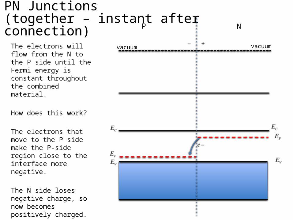
The electrons will flow from the N to the P side until the Fermi energy is constant throughout the combined material.
How does this work?
The electrons that move to the P side make the P-side region close to the interface more negative.
The N side loses negative charge, so now becomes positively charged.
PN Junctions (together – instant after connection)
vacuum
P
vacuum
N

This space charge region near the junction sets up a local electric field, from the positive to the negative charge.
Now an electron in the vacuum just outside the interface will also sense this field and have a larger energy on the P side.
PN Junctions (together – dipole formation)
vacuum
P
vacuum
N

This increase in energy of the P side must drag up all the bands along with it.
The bands far away from the junction are the same as the bare doped materials. Just their relative offsets have changed. This potential offset is only a relative quantity anyway.
The potential drop is called the “built-in potential” of the interface.
This potential is the source of power in a semiconductor solar cell.
PN Junctions (together – band bending) vacuum
P
vacuum
N

This built-in potential drop is very strange – it is saying that we have a voltage drop just by placing two materials together.
Remember
Does this mean that we can just stick two materials together to form a battery, without any other energy costs?
No!!
PN Junctions (An electric without current?) vacuum
P
vacuum
N

What do we control with a voltage source – eg, a battery?
The Fermi energy – which is also called the “electro-chemical potential”. It’s the energy cost of adding another electron in that vicinity – taking electrostatic energy and the band energy both into account.
This equation is for a uniform material.
PN Junctions (a voltage source controls the Fermi energy) vacuum

In a uniform material, the Fermi energy and the electrostatic potential are parallel to each other. This makes a distinction between the two unimportant in this case, and
is valid.
The electrons get accelerated by the field and then relax back to a steady-state distribution which is not the same as the equilibrium distribution.
PN Junctions (a voltage source controls the Fermi energy)
vacuum
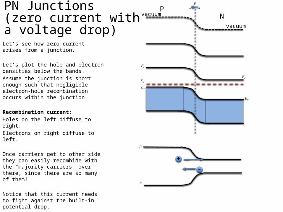
Let’s see how zero current arises from a junction.
Let’s plot the hole and electron densities below the bands.Assume the junction is short enough such that negligible electron-hole recombination occurs within the junction
Recombination current:Holes on the left diffuse to right. Electrons on right diffuse to left.
Once carriers get to other side they can easily recombine with the “majority carriers” over there, since there are so many of them!
Notice that this current needs to fight against the built-in potential drop.
PN Junctions (zero current witha voltage drop)
vacuumP
vacuum
N
+-

Generation current:Although there are not as many holes on the right and electrons on the left, the potential drop will easily sweep any of these “minority” carriers to the other side. Likewise for the electrons on the left side.
Since this current is only limited by the relatively low generation rate of minority carriers on either side of the junction, it is called a “generation current”.
PN Junctions (zero current witha voltage drop)
vacuumP
vacuum
N
+
-

Zero current (equilibrium condition):For zero current everywhere, the two currents across the junction must sum to zero.
Thus,
for .
PN Junctions (zero current witha voltage drop)
vacuumP
vacuum
N

What do we control with a voltage source – eg, a battery?
The Fermi energies on either side of the junction!
Where will this applied energy change cause an electrochemical potential (Fermi energy) drop?
Near the PN junction interface.This is where we have the lowest conductivity. Even though the product of p and n is constant throughout in equilibrium – the sum is not!!
PN Junctions (applying a voltage) vacuum
P
vacuum
N
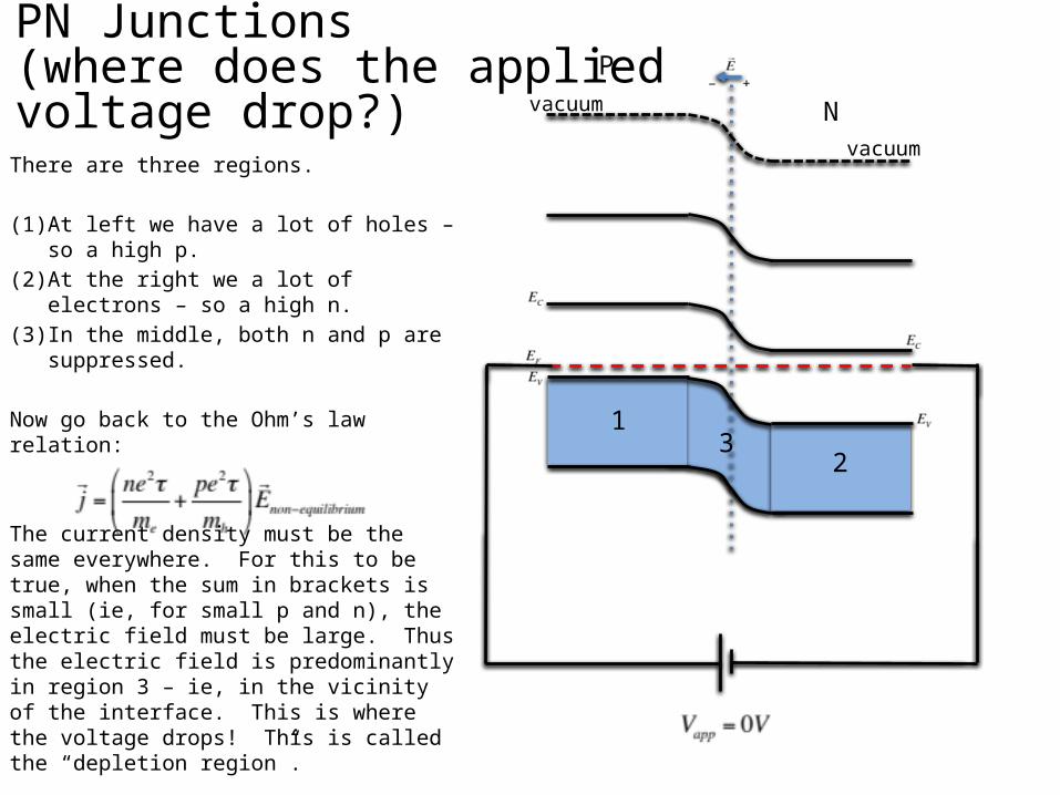
There are three regions.
(1) At left we have a lot of holes – so a high p.
(2) At the right we a lot of electrons – so a high n.
(3) In the middle, both n and p are suppressed.
Now go back to the Ohm’s law relation:
The current density must be the same everywhere. For this to be true, when the sum in brackets is small (ie, for small p and n), the electric field must be large. Thus the electric field is predominantly in region 3 – ie, in the vicinity of the interface. This is where the voltage drops! This is called the “depletion region”.
PN Junctions (where does the appliedvoltage drop?) vacuum
P
vacuum
N
1
23

Consider a negative applied voltage.
Fermi energies on either side of the junction are no longer the same. These are called “quasi Fermi levels” (they are not in equilibrium).
This results in a wider region with reduced carriers (the depletion region has increased in width).
The generation current will be the same as before, but the recombination current will be significantly reduced due to the increase in barrier size.
PN Junctions (applied voltage < 0)
vacuumP
vacuum
N

Consider the current density across the solid blue line due to electrons. Holes will behave similarly.
The recombination current for electrons is proportional to probability for an electron to be in the conduction band on p-side.
PN Junctions (applied voltage < 0)
vacuumP
vacuum
N
--
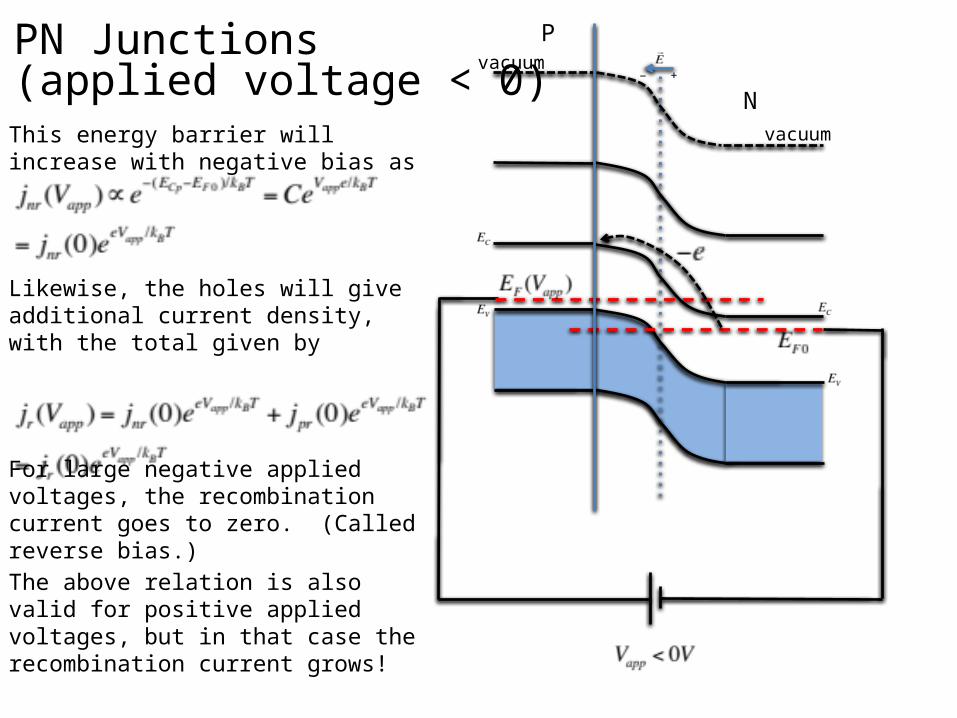
This energy barrier will increase with negative bias as
Likewise, the holes will give additional current density, with the total given by
For large negative applied voltages, the recombination current goes to zero. (Called reverse bias.)The above relation is also valid for positive applied voltages, but in that case the recombination current grows!
PN Junctions (applied voltage < 0)
vacuumP
vacuum
N

The recombination current is the only one that changes with voltage – the generation current remains unchanged.The total is
or
which the ideal diode behavior of a PN junction.
This is the rectifying behavior of a diode. It only passes a large current in one direction!!This is useful if you want to convert AC signals to DC, among many other uses!!
PN Junctions (total current)
In our derivation we assumed the depletion width was narrow enough such that recombination only occurred outside of it. If appreciable recombination occurs within the depletion with, this alters the form through an “ideality factor” , where

When a forward bias is applied across the junction a large amount of recombination occurs and the diode will emit light principally at the band gap energy. This is a light emitting diode (LED) and is an efficient source of light compared to a light bulb (which emits and entire black-body radiation spectrum)
PN junction solar cells utilize the built-in potential of the junction. If light excites a hole-electron pair in the vicinity of the junction, the built-in potential will separate the two carriers and can drive a current through an external circuit.
Some Other Uses of PN Junctions
vacuum
P
vacuum
N

Transistors are central to modern electronics. They are electronic switches which are at the heart of circuitry inside a computer which can perform calculations.
Transistors can be built up of two PN junctions – these are call bipolar transistors. Another form principally uses the properties of a single semiconductor – the field effect transistor (FET).
If you connect a semiconductor to two metals or highly doped semiconductors, we can have the bands shown at right.This assumes an n-doped semiconductor in the middle channel region.
Transistors vacuum
electrode electrode
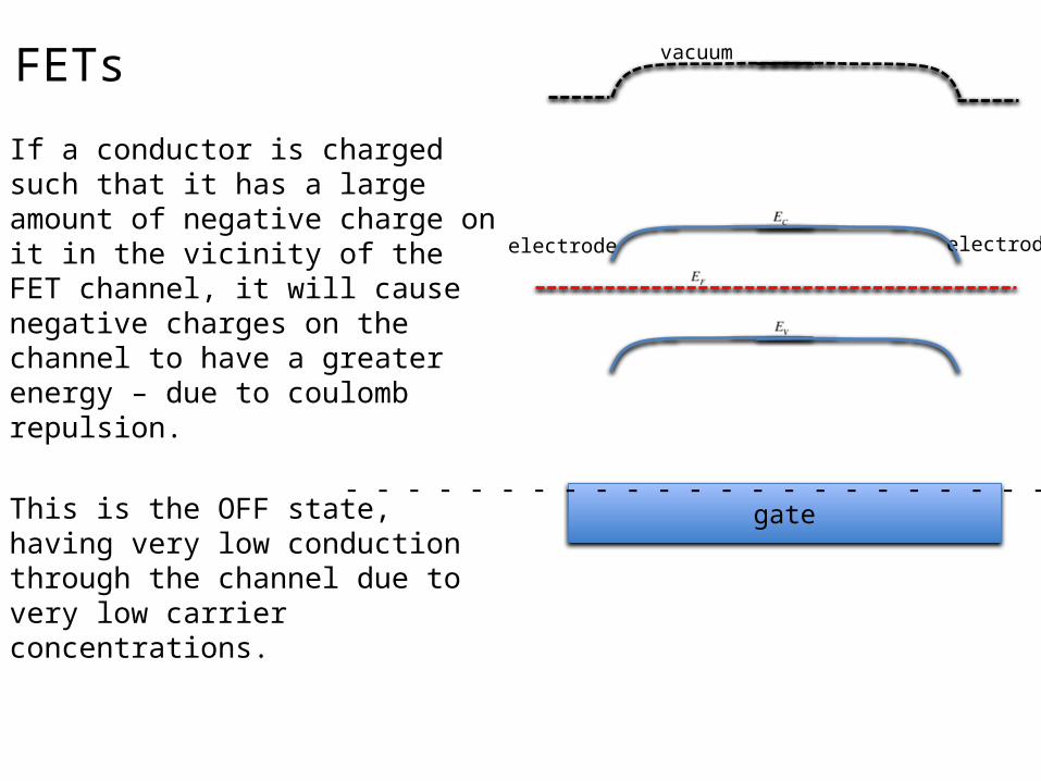
If a conductor is charged such that it has a large amount of negative charge on it in the vicinity of the FET channel, it will cause negative charges on the channel to have a greater energy – due to coulomb repulsion.
This is the OFF state, having very low conduction through the channel due to very low carrier concentrations.
FETs vacuum
electrode electrode
gate- - - - - - - - - - - - - - - - - - - - - - - - - - - - -

For an opposite charge on the conductor – positive – we have the energy of electrons reduced on the channel.
This is the ON state, having very high conduction through the channel due to a very high carrier concentration.
At the interface, we can still have regions of low carrier concentrations which act as barriers. For short channels (important in nanotechnology applications) this barrier impedance is an appreciable contribution compared to the rest of the channel, so is very important.
FETs vacuum
electrode electrode
gate ++++++++++++++++++++++++++++++

“Light Amplification by Stimulated Emission of Radiation”
While the first lasers were gas chambers -- laser diodes were discovered shortly afterwards and have grown in popularity ever since.
By forward biasing this diode the Fermi levels on either side of the diode split by the applied voltage and the bands bend.
LASERs
GaAs
p-AlxGa1-xAs
n-AlxGa1-xAs

“Light Amplification by Stimulated Emission of Radiation”
While the first lasers were gas chambers -- laser diodes were discovered shortly afterwards and have grown in popularity ever since.
By forward biasing this diode the Fermi levels on either side of the diode split by the applied voltage and the bands bend.
LASERs GaAsp-AlxGa1-xAs n-AlxGa1-xAs

This results in a large number of electrons and holes in the thin GaAs layer which can easily recombine. When they recombine, the energy goes into a photon given approximately by the bandgap of the well (the small band gap region).
The random recombination does not produce the lasing effect.
To achieve lasing requires stimulated emission.
LASERs GaAsp-AlxGa1-xAs n-AlxGa1-xAs

Photons obey very different statistics than electrons and fermions. Photons are bosons, which do not obey the Pauli Exclusion Principle. Photons can and actually tend to be in the same state.
The distribution function for bosons is the Bose-Einstein distribution function.
At low temperatures, bosons tend to all fill the same ground state.
Photon Statistics GaAsp-AlxGa1-xAs n-AlxGa1-xAs

This tendency for photons to occupy the same state can drive an electronic transition to produce a photon in the same state as an already existing photon.
To produce a laser, one uses mirrors on the two ends of the diode stack to bounce the light back and forth between them. As the light bounces back and forth it stimulates electronic transitions producing photons exactly in phase and with the same polarization as the original photons.
One of the mirrors can be replaced with a slightly transparent mirror, which allows some of the laser light out so that it can be used – for example as a pointer.
Stimulated Emission GaAsp-AlxGa1-xAs n-AlxGa1-xAs
mirror
semi-transparent mirror
light out