physical review applied 9, 021002 (2018)
TRANSCRIPT
Stretchable Kirigami Polyvinylidene Difluoride Thin Films for Energy Harvesting:Design, Analysis, and Performance
Nan Hu,1,2 Dajing Chen,1,3 Dong Wang,1,4 Shicheng Huang,1 Ian Trase,1 Hannah M. Grover,1
Xiaojiao Yu,1 John X. J. Zhang,1,* and Zi Chen1,†1Thayer School of Engineering, Dartmouth College, Hanover, New Hampshire 03755, USA2Department of Civil, Environmental and Geodetic Engineering, The Ohio State University,
Columbus, Ohio 43210, USA3Medical School, Hangzhou Normal University, Hangzhou, Zhejiang 311121, China
4The Science Cluster, Singapore University of Technology and Design, 487372 Singapore, Singapore
(Received 28 April 2017; revised manuscript received 2 November 2017; published 22 February 2018)
Kirigami, a modified form of origami which includes cutting, has been used to improve materialstretchability and compliance. However, this technique is, so far, underexplored in patterning piezoelectricmaterials towards developing efficient and mechanically flexible thin-film energy generators. Motivated byexisting kirigami-based applications, we introduce interdigitated cuts to polyvinylidene fluoride (PVDF)films to evaluate the effect on voltage generation and stretchability. Our results from theoretical analysis,numerical simulations, and experimental tests show that kirigami PVDF films exhibit an extended strainrange while still maintaining significant voltage generation compared to films without cuts. Various cuttingpatterns are studied, and it is found that films with denser cuts have a larger voltage output. This kirigamidesign can enhance the properties of existing piezoelectric materials and help to integrate tunable PVDFgenerators into biomedical devices.
DOI: 10.1103/PhysRevApplied.9.021002
Kirigami, a variation of origami that introduces cutting,can create complex 3D geometries from flat 2D sheetsthrough out-of-plane deformations. A wide range of tech-nologieshavebeen inspiredbykirigami [1].At thenanoscale,kirigami has enabled the shape formation and self-assemblyof3Dnanostructures from2Dsheets.Examples includeDNAnanotechnology [2], nanomembranes [3], and nanoelectro-mechanical systems [4]. Blees et al. [5] designed kirigamigraphene sheets to achieve large ductility and resilience forstretchable electronics and photovoltaics. Based upon thiswork, the introduction of kirigami molybdenum disulfidehas significantly increased yield and fracture strains [6].Similarly, Shyu et al. [7] created kirigami nanocompositesthat can extend ultimate strain up to 370%. At larger scales,kirigamihas inspirednoveldesigns inbiosensing [8], steeringmechanisms [9], cellular metamaterials [10], reconfigurablemetamaterials [11], bioprobe devices [12], stretchable lith-ium-ion batteries [13], solar tracking systems [14], adaptivemorphing wings [15], energy dissipation structures [16], andenergy-efficientbuildingskins [17].Whilemost studies focuson modifying geometry and morphology to achieve highstretchability [18], there has been a recent emphasis on
mechanical instability related to origami and kirigami.Mechanical instabilities can be a favorable phenomenonfor smart materials [19], and stimuli responsive systems[20,21]. For example, 3Dmicrostructures and nanostructureswere fabricated via the compressive buckling of filamentaryribbons, whose tunable geometric features enabled the rapidassembly of stimuli responsive structures [22].In this Letter, we use kirigami to improve the ability of
piezoelectric materials to act as a power source for portableand implantable devices. In recent years, several flexible,stretchable devices have been developed for energy harvest-ing [23], self-power generation [24], spatiotemporal cardiacmeasurements [25], motion detection of fingers [26], wear-able electronic devices [27], and high-strain sensors [28].Among the many types of piezoelectric materials, polyvi-nylidene fluoride (PVDF) is the most promising for bio-medical applications due to its low cost, light weight,mechanical performance, and excellent biocompatibility.Current PVDF-based devices are mostly 2D structures,limited to in-plane deformation. Our previous studies onPVDF films have demonstrated their potential for energygeneration [29] with both symmetric and asymmetric poredistribution [30]. Porous PVDF films, for example, haveenabled a new generation of minimally invasive glucosesensors [31]. We introduce patterned cuts on PVDF films toinduce out-of-plane deformation. The hypothesis is thatkirigami can increase the strain range of piezoelectric
*Corresponding [email protected]
†Corresponding [email protected]
PHYSICAL REVIEW APPLIED 9, 021002 (2018)Letter
2331-7019=18=9(2)=021002(6) 021002-1 © 2018 American Physical Society

structures while still maintaining significant energy gener-ation. We envision that the tunability of kirigami can beapplied to multifunctional piezoelectric devices such asbiomedical devices.As a proof of concept, we began by fabricating baseline
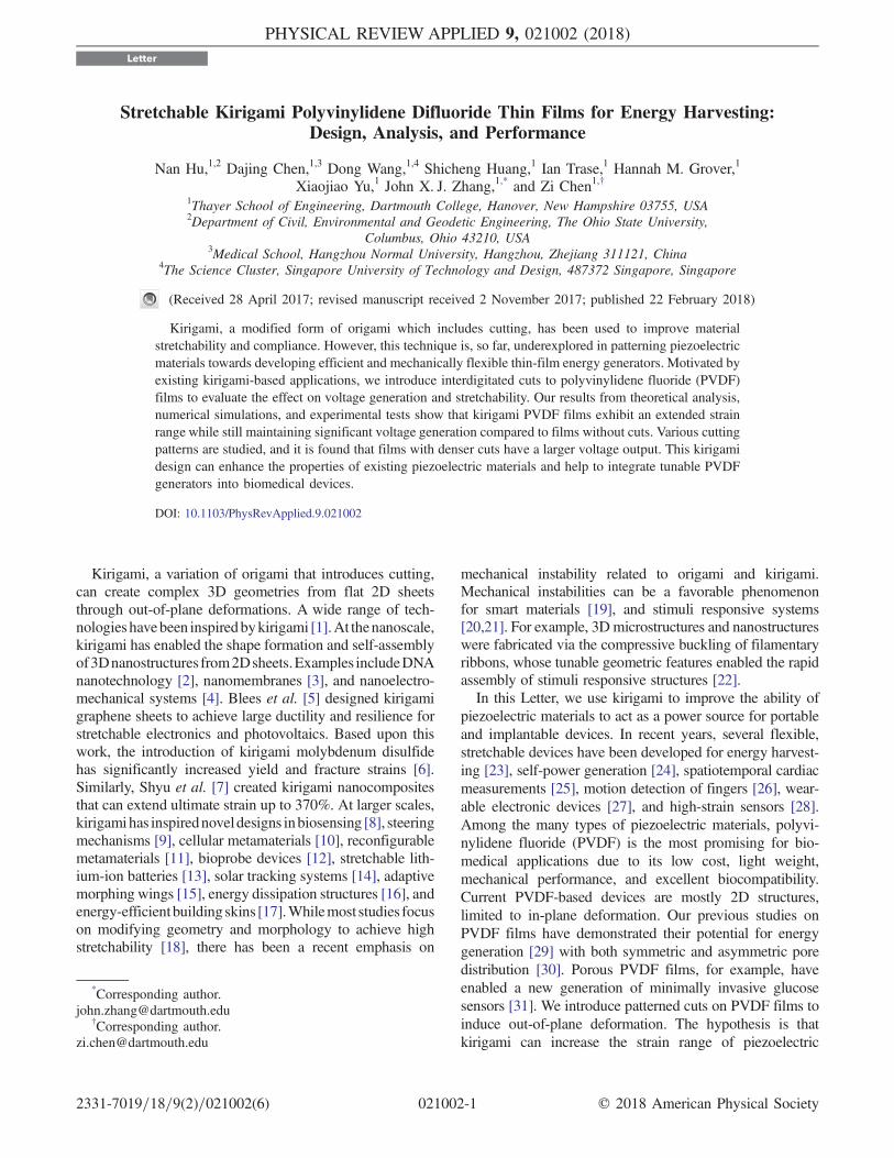
solid PVDF films (see the Supplemental Material [32]).Figure 1(a) shows a thin film 30 mm long, 15 mmwide, and50 μm thick. The 200-nm-thick electrodes are deposited onthe PVDF layer (25 μm) by an E-beam evaporator. Thebottom Kapton film, with a thickness of 25 μm, is used as asupporting substrate to increase the stiffness of the speci-men. We use a scalpel to cut the baseline PVDF films withtwo different patterns, center cutting and edge cutting. Itshould be noted that noncutting regions of 6 mm arereserved on each end of the PVDF film for an electricalconnection to measurement circuitry. As a result, cuts areonly applied to the middle portion of the film (18 mm). Thecenter-cutting design has the cut length of 10 mm in thecenter and 5 mm on the edge, while the edge-cutting designcontains only 10-mm-long cuts along the edge. PVDF filmswith both cutting patterns are uniaxially stretched with amotorized test stage. The maximum load (0.75 N) is setconstant, since the piezoelectric output is directly related tothe stress applied. We put a force gauge at one end of thekirigami structure during testing. A load-limiting test isused, as the moving stage will automatically stop once itreaches the maximum load.
After measuring the voltage output through the chargeamplifier, we compare the performance of PVDF films withand without cuts. Figure 1(b) shows the deformed shape ofthe two cutting patterns. The strain in our experiment is aneffective strain, defined as the elongation divided by theoriginal length. As expected, the PVDF filmwithout cuts hasa larger voltage output (160 mV) yet a smaller strain (1%).Kirigami-based PVDF films, in contrast, attain a slightlysmaller voltage output but can attain strains of up to 18%without fracture. Note that the film with the center-cuttingpattern has a larger voltageoutput (132mV) than the onewiththe edge-cutting pattern (85mV). Themain contributor to thevoltage output is the stress due to the in-plane surfacestretching of the film. The center-cutting design has a largerportion of surface area under tensile stress during thestretching process, so it has a larger voltage output.We characterized the response of the center-cut PVDF
under axial stretching using finite element (FE) software(ABAQUS, standard version 6.14), as shown in Video 1(a).The kirigami PVDF films are designed in SOLIDWORKS andthen imported to ABAQUS. The 3D solid geometry of thePVDF film is meshed with the C3D20RE element type andthe Kapton film is meshed with the C3D20R element type.We do not include the aluminum layers due to the lesssignificant thickness (200 nm) compared to the thicknessesof the PVDF and Kapton layers. The Young’s modulus of
FIG. 1. The design and performance ofkirigami PVDF films. (a) Baseline filmwithout cuts and kirigami patterns.(b) Piezoelectric output between PVDFfilms with and without cuts.
VIDEO 1. Simulationof kirigami PVDF filmsunder axial stretching.(a) Stress-strain curvefor a PVDF film withcenter cuts. (b) Compari-son of electric charges inPVDF film with centercutting between experi-ment and simulation.
NAN HU et al. PHYS. REV. APPLIED 9, 021002 (2018)
021002-2
the PVDF film is 1.53 GPa and the Poisson’s ratio is 0.37.The dielectric constant of the PVDF film is 1.06 × 10⁻¹⁰and its piezoelectric properties d31 and d33 are −21 ×10−12 C=N and −29 × 10−12 C=N, respectively. TheYoung’s modulus of the Kapton film is 2.5 GPa and thePoisson’s ratio is 0.34. An axial load is applied at oneend while a clamped condition is applied at the other.Simulations are performed using a dynamic implicit solver.A synchronized video featuring the stress-strain curve andcharge-strain curve is shown in Video 1. Video 1(a) shows
two regimes in the force-displacement curve divided by acritical buckling load. Prior to the critical point, the filmonly undergoes in-plane deformation. A drop in force isobserved after the critical point, indicating the onset of out-of-plane deformation. Numerically, the buckling of the filmis triggered due to the asymmetric mesh of the computa-tional model. The load magnitude then increases linearly asthe stretching process continues. Excellent deformed shapeagreement is found between experiments and finite elementsimulations. The von Mises stress is defined as
σVM ¼ffiffiffiffiffiffiffiffiffiffiffiffiffiffiffiffiffiffiffiffiffiffiffiffiffiffiffiffiffiffiffiffiffiffiffiffiffiffiffiffiffiffiffiffiffiffiffiffiffiffiffiffiffiffiffiffiffiffiffiffiffiffiffiffiffiffiffiffiffiffiffiffiffiffiffiffiffiffiffiffiffiffiffiffiffiffiffiffiffiffiffiffiffiffiffiffiffiffiffiffiffiffiffiffiffiffiffiffiffiffiffiffiffiffiffiffiffiffiffiffiffiffiffiffiffiffiffiffiffiffiffi
½ðσ11 − σ22Þ2 þ ðσ22 − σ33Þ2 þ ðσ33 − σ11Þ2�=2þ 3ðτ212 þ τ223 þ τ213Þq
;
where σ11, σ22, σ33 are normal stresses and τ12, τ23, τ13 areshear stresses, which is widely used to predict the yieldingof materials under complex loading. Here, the distributionsof the von Mises stress from the simulation are plotted asinsets in Video 1(a). It can be seen that a higher von Misesstress (lighter color) is observed at sharp corners of cuts,which does limit the stretchability of the film. In fact, arecent study [7] has found that the kirigami structures canbe further stretched after introducing rounded edges atthese sharp corners. Thus, the investigation on the stressredistribution and optimization of the kirigami PVDF isbeyond the scope of this work.We further validate the accuracy of our numerical
model by comparing the charge output obtained from theexperiment and the estimated charge output from thenumerical model, see Video 1(b). The experimental valueof the electric charge is calculated byQ ¼ CðV=AVDÞ, whereC is the feedback capacitor used in the charge amplifier(10 × 10−9 F); V is the voltage measured by charge ampli-fier; and AVD is the amplifier voltage gain (110 V). Forexample, the electric charge when the measured voltage at6% strain (22 mV) is 2.00 × 10⁻¹² C while the simulatedcharge is 1.92 × 10⁻¹² C. In the simulation, we request atotal of ten data points to show the changing of the total
charge within the film. It can be seen that after the filmbuckles at 4% strain, a significant jump is observed in thetotal electric charge output. The simulated electric charge isless than those experimental data, but the error betweenexperiment and simulation is acceptable.We have demonstrated that kirigami PVDF films have an
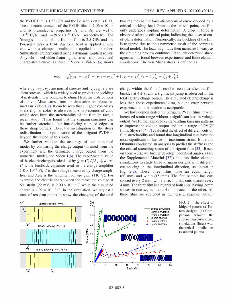
increased strain range without a significant loss in voltageoutput. We further explored center-cutting kirigami patternsto improve the voltage output and strain range of PVDFfilms. Shyu et al. [7] evaluated the effect of different cuts onfilm stretchability and found that longitudinal cuts have themost significant influence on maximum strain. Isobe andOkumura conducted an analysis to predict the stiffness andthe critical stretching strain of a kirigami film [33]. Basedon their work, we further develop theoretical analysis (seethe Supplemental Material [32]) and run finite elementsimulations to study three kirigami designs with differentcut spacing in the longitudinal direction, as shown inFig. 2(a). These three films have an equal length(60 mm) and width (15 mm). The first sample has cutsspaced every 2 mm, while a second has cuts spaced every4 mm. The third film is a hybrid of both cuts, having 2-mmspaces in one segment and 4-mm spaces in the other. Allthree films are stretched in their elastic regimes without
FIG. 2. The effect ofkirigami pattern. (a) Pat-tern designs. (b) Com-parison between thestress-strain curves fromsimulations (lines) withtheoretical predictions(scattered points).
STRETCHABLE KIRIGAMI POLYVINYLIDENE … PHYS. REV. APPLIED 9, 021002 (2018)
021002-3

considering material damage. We plot the stress vs straincurve of the hybrid cut design and two single-cut designsin Fig. 2(b). The response of a kirigami film transitionsbetween two regimes: in-plane and out-of-plane deforma-tion. In the hybrid design, the dense segment (2 mm) movesinto the postbuckling, out-of-plane regime before the sparsesegment (4 mm). At this point, the sparse-spacing segmentis not fully stretched due to a large stress concentration atthe interface between two segments. In Fig. 2(b) we plot thetheoretical analysis as scatter points to compare with thenumerical simulation results. A good agreement betweensimulation and theoretical analysis is observed.We fabricate the above-mentioned films along with a
baseline design without cuts and measure their voltageoutputs through a charge amplifier (Fig. 3). These newfilms have a total length of 60 mm rather than the 30 mm ofprevious films. The voltage output of the PVDF filmwithout cuts (325 mV) in the 60-mm-long film is doublethat of the previous 30-mm-long film (160 mV). The cutlengths stay the same as those in Fig. 1. As we stretch thefilms with cuts to about 20% strain, the dense design has alarger voltage output (283 mV) than both the hybrid designand the sparse design. At 20% strain the sparsely cut filmis fully stretched, and we observe larger strain limits forboth the hybrid design (24%) and the dense design (33%).This stretchability is above the general upper limit for skin(20%). The voltage output (296 mV) associated with thehybrid design is approximately the same as the one withoutcuts, while the voltage output (333 mV) of the dense designeven exceeds the cut-free film. This phenomenon is similarto the one we observe in Fig. 1, the underlying reason ofwhich is that the main contributor to the voltage output isthe stress due to the in-plane surface stretching of the film.In the sparse design, the film is limited by the stressdistribution at those sharp corners, which in turn cause alower stress on the other locations of the film surface. Thedenser design has a higher stress at other locations of thefilm, which leads to a higher voltage generation.
Among the patterns, the dense design has the largestnumber of cuts and sharp corners, and has the largestvoltage output, which might indicate a correlation betweenthese two parameters. The hybrid design is not fullystretched, as we observe cracks at the interface betweenthe dense and the sparse portions of the film. Other designsalso have the same damage at sharp corners. We also testperformance when the film is subjected to several stretch-ing cycles. The dense design has a mean average of 340 mVfor the voltage output but becomes damaged after fiveloading cycles. If we stretch the same film at a strain level5% less than the limit of 33%, the voltage output remains at299 mV without any damage.In summary, we introduce interdigitated and other
patterned cuts on PVDF thin films to enhance energygeneration ability. Supported by theoretical analysis, FEsimulations, and experiments, we show that axiallystretched kirigami PVDF films can attain a much higherstrain limit (30%) while maintaining the same level ofvoltage output compared to regular PVDF films. Thecurrent designs can be extended beyond the componentlevel, towards the exploration of biaxial stretching and 3Dsystem assembly. As high strains will likely be observedin the potential design of wearable and implantabledevices (such as electronic clothes and finger posturedetection), piezoelectric PVDF-trifluoroethylene films, incombination with a careful design of supporting mechani-cal membranes, can be used to make flexible devices.We believe the concept of kirigami-patterned functionalthin films can also be applied to other types of energyharvesters such as patch-based thin plates [34] andorigami-based structures [35]. State-of-the-art piezoelec-tric polymer-based devices rely on thin-film geometries.These conventional devices have been intensively studiedbut have not proven capable of achieving sufficientlyhigh voltage output. Our study shows that kirigami-based piezoelectric materials can enhance piezoelectricoutput with extended stress-strain responses for high-efficiency power generation devices. We envision apromising future in which kirigami-based piezoelectricmaterials are fully adapted into self-powered biomedicaldevices.
Note: Dartmouth College has filed a patent applicationrelating to the use of kirigami structures for energyharvesting based on the results of this study.
ACKNOWLEDGMENTS
Z. C. acknowledges the startup fund from the ThayerSchool of Engineering at Dartmouth and the support fromthe Branco Weiss–Society in Science Fellowship, admini-stered by ETH Zürich. X. J. Z. acknowledges the supportfrom the NIH Director’s Transformative Research Award(No. R01HL137157), and NSF Grants No. ECCS 1128677,No. 1309686, and No. 1509369. We gratefully acknowl-edge the support from the Microfabrication and Electron
FIG. 3. Measured voltage output and strain for different cuttingpatterns. Inset: deformed configuration of kirigami PVDF filmafter stretching.
NAN HU et al. PHYS. REV. APPLIED 9, 021002 (2018)
021002-4
Microscope Facility at Dartmouth College. N. H. acknowl-edges the startup fund from the College of Engineering atThe Ohio State University.
N. H. and D. C. contributed equally to this work.
[1] G. P. Collins, Science and culture: Kirigami and technologycut a fine figure, together, Proc. Natl. Acad. Sci. U.S.A. 113,240 (2016).
[2] D. Han, S. Pal, Y. Liu, and H. Yan, Folding and cuttingDNA into reconfigurable topological nanostructures, Nat.Nanotechnol. 5, 712 (2010).
[3] F. Cavallo and M. G. Lagally, Nano-origami: Art andfunction, Nano Today 10, 538 (2015).
[4] Z. Chen, G. Huang, I. Trase, X. Han, and Y. Mei,Mechanical Self-Assembly of a Strain-Engineered FlexibleLayer: Wrinkling, Rolling, and Twisting, Phys. Rev.Applied 5, 017001 (2016).
[5] M. K. Blees, A.W. Barnard, P. A. Rose, S. P. Roberts, K. L.McGill, P. Y. Huang, A. R. Ruyack, J. W. Kevek, B. Kobrin,D. A. Muller, and P. L. McEuen, Graphene kirigami, Nature(London) 524, 204 (2015).
[6] P. Z. Hanakata, Z. Qi, D. K. Campbell, and H. S. Park,Highly stretchable MoS2 kirigami, Nanoscale 8, 458(2016).
[7] T. C. Shyu, P. F. Damasceno, P. M. Dodd, A. Lamoureux, L.Xu, M. Shlian, M. Shtein, S. C. Glotzer, and N. A. Kotov, Akirigami approach to engineering elasticity in nanocompo-sites through patterned defects, Nat. Mater. 14, 785(2015).
[8] L. Xu, X. Wang, Y. Kim, T. C. Shyu, J. Lyu, and N. A.Kotov, Kirigami nanocomposites as wide-angle diffractiongratings, ACS Nano 10, 6156 (2016).
[9] W. Wang, C. Li, H. Rodrigue, F. Yuan, M.-W. Han, M. Cho,and S.-H. Ahn, Kirigami/origami-based soft deployablereflector for optical beam steering, Adv. Funct. Mater.27, 1604214 (2017).
[10] M. Eidini and G. H. Paulino, Unraveling metamaterialproperties in zigzag-base folded sheets, Sci. Adv. 1,e1500224 (2015).
[11] A. Rafsanjani and K. Bertoldi, Buckling-Induced Kirigami,Phys. Rev. Lett. 118, 084301 (2017).
[12] Y. Morikawa, S. Yamagiwa, H. Sawahata, M. Ishida, andT. Kawano, in Proceedings of the 2016 IEEE 29thInternational Conference on Micro Electro MechanicalSystems (MEMS) (IEEE, New York, 2016), p. 149.
[13] Z. Song, X. Wang, C. Lv, Y. An, M. Liang, T. Ma, D. He,Y.-J. Zheng, S.-Q. Huang, H. Yu, and H. Jiang, Kirigami-based stretchable lithium-ion batteries, Sci. Rep. 5, 10988(2015).
[14] A. Lamoureux, K. Lee, M. Shlian, S. R. Forrest, and M.Shtein, Dynamic kirigami structures for integrated solartracking, Nat. Commun. 6, 8092 (2015).
[15] K. Saito, F. Agnese, and F. Scarpa, A cellular kirigamimorphing wingbox concept, J. Intell. Mater. Syst. Struct. 22,935 (2011).
[16] Y. Hou, R. Neville, F. Scarpa, C. Remillat, B. Gu, and M.Ruzzene, Graded conventional-auxetic Kirigami sandwich
structures: Flatwise compression and edgewise loading,Composites Part B 59, 33 (2014).
[17] Y. Tang, G. Lin, S. Yang, Y. K. Yi, R. D. Kamien, and J. Yin,Programmable Kiri-Kirigami Metamaterials, Adv. Mater.29, 1604262 (2017).
[18] D. M. Sussman, Y. Cho, T. Castle, X. Gong, E. Jung, S.Yang, and R. D. Kamien, Algorithmic lattice kirigami: Aroute to pluripotent materials, Proc. Natl. Acad. Sci. U.S.A.112, 7449 (2015).
[19] N. Hu and R. Burgueño, Buckling-induced smart applica-tions: Recent advances and trends, Smart Mater. Struct. 24,063001 (2015).
[20] Z. Chen, Q. Guo, C. Majidi, W. Chen, D. J. Srolovitz, andM. P. Haataja, Nonlinear Geometric Effects in MechanicalBistable Morphing Structures, Phys. Rev. Lett. 109, 114302(2012).
[21] Q. Guo, A. K. Mehta, M. A. Grover, W. Chen, D. G. Lynn,and Z. Chen, Shape selection and multi-stability in helicalribbons, Appl. Phys. Lett. 104, 211901 (2014).
[22] S. Xu et al., Assembly of micro/nanomaterials into com-plex, three-dimensional architectures by compressive buck-ling, Science 347, 154 (2015).
[23] Y. Qi, J. Kim, T. D. Nguyen, B. Lisko, P. K. Purohit, andM. C. McAlpine, Enhanced piezoelectricity and stretchabil-ity in energy harvesting devices fabricated from buckledPZT ribbons, Nano Lett. 11, 1331 (2011).
[24] W. Wu, S. Bai, M. Yuan, Y. Qin, Z. L. Wang, and T. Jing,Lead zirconate titanate nanowire textile nanogenerator forwearable energy-harvesting and self-powered devices, ACSNano 6, 6231 (2012).
[25] L. Xu et al., 3D multifunctional integumentary membranesfor spatiotemporal cardiac measurements and stimulationacross the entire epicardium, Nat. Commun. 5, 3329(2014).
[26] M. Amjadi, A. Pichitpajongkit, S. Lee, S. Ryu, and I. Park,Highly stretchable and sensitive strain sensor based on silvernanowire–elastomer nanocomposite, ACS Nano 8, 5154(2014).
[27] J. T. Muth, D. M. Vogt, R. L. Truby, Y. Mengüç, D. B.Kolesky, R. J. Wood, and J. A. Lewis, Embedded 3Dprinting of strain sensors within highly stretchable elasto-mers, Adv. Mater. 26, 6307 (2014).
[28] C. Yan, J. Wang, W. Kang, M. Cui, X. Wang, C. Y. Foo,K. J. Chee, and P. S. Lee, Highly stretchable piezoresistivegraphene–nanocellulose nanopaper for strain sensors, Adv.Mater. 26, 2022 (2014).
[29] D. Chen, T. Sharma, and J. X. J. Zhang, Mesoporous surfacecontrol of PVDF thin films for enhanced piezoelectricenergy generation, Sens. Actuators A 216, 196 (2014).
[30] D. Chen and J. X. J. Zhang, Microporous polyvinylidenefluoride film with dense surface enables efficient piezo-electric conversion, Appl. Phys. Lett. 106, 193901 (2015).
[31] D. Chen, C. Wang, W. Chen, Y. Chen, and J. X. J. Zhang,PVDF-Nafion nanomembranes coated microneedles forin vivo transcutaneous implantable glucose sensing,Biosens. Bioelectron. 74, 1047 (2015).
[32] See Supplemental Material at http://link.aps.org/supplemental/10.1103/PhysRevApplied.9.021002 for thekey fabrication steps of PVDF films, theoretical derivationof films with hybrid pattern, and a movie of simulated
STRETCHABLE KIRIGAMI POLYVINYLIDENE … PHYS. REV. APPLIED 9, 021002 (2018)
021002-5

stress-strain response and electric charge output for a PVDFfilm with center cutting.
[33] M. Isobe and K. Okumura, Initial rigid response andsoftening transition of highly stretchable kirigami sheetmaterials, Sci. Rep. 6, 24758 (2016).
[34] B. Bayik, A. Aghakhani, I. Basdogan, and A. Erturk,Equivalent circuit modeling of a piezo-patch energy
harvester on a thin plate with AC-DC conversion, SmartMater. Struct. 25, 055015 (2016).
[35] P.-K. Yang, Z.-H. Lin, K. C. Pradel, L. Lin, X. Li, X. Wen,J.-H. He, and Z. L. Wang, Paper-based origami triboelectricnanogenerators and self-powered pressure sensors, ACSNano 9, 901 (2015).
NAN HU et al. PHYS. REV. APPLIED 9, 021002 (2018)
021002-6