photorefraction in tin hypothiodiphosphate in the near infrared
TRANSCRIPT
2352 J. Opt. Soc. Am. B/Vol. 13, No. 10 /October 1996 Odoulov et al.
Photorefraction in tin hypothiodiphosphate in thenear infrared
Serguey G. Odoulov and Alexander N. Shumelyuk
Institute of Physics, National Academy of Sciences, 252 650, Kiev-22, Ukraine
Ute Hellwig* and Romano A. Rupp
Department of Physics, Universitat Osnabruck, 49069 Osnabruck, Germany
Alexander A. Grabar and Ivan M. Stoyka
Institute of Solid State Physics and Chemistry, Uzhgorod State University, 294 000, Uzhgorod, Ukraine
Ferroelectric photorefractive Sn2P2S6 crystals become more sensitive to cw radiation of a Nd31: YAG laser (l5 1.06 mm) by preexposure with incoherent white light. Space-charge formation and hologram recording aredominated by a diffusionlike charge transport, leading to an ultimate gain factor for transmission gratingsthat exceeds 6 cm21 at a laser intensity of approximately 50 W/cm2. © 1996 Optical Society of America.
1. INTRODUCTION
Photorefractive materials for the near-infrared region ofthe spectrum are attractive because they can successfullybe used with the continuously increasing number of semi-conductor lasers of improved performance. On the onehand, they can be used to manipulate the output beams ofthese lasers: to clean up the laser beams,1 to conjugatetheir wave fronts,2 to couple it to optical fibers,3 etc. Onthe other hand, they can be effective for the improvementof semiconductor lasers themselves, e.g., for synchroniza-tion of laser-diode arrays.4 A rather high couplingstrength Gl of the recorded dynamic grating is needed formost of these applications. To obtain coherent self-oscillation in, e.g., a double-phase-conjugate mirror, thecondition Gl . 4 should be fulfilled,5 i.e., G should exceed4 cm21 for a typical thickness l 5 1 cm of the sample.In principle it is possible to obtain even higher gain fac-tors in semiconductor photorefractive crystals such asGaAs, InP, or CdTe, but this usually requires the solutionof some serious technical problems: application of highdc or ac fields,6 special adjustment of the laser wave-length close to the absorption edge,7 or adjustment of thetemperature of the sample and/or of the intensity of therecording waves.8
Recently the magic rhodium-doped BaTiO3 crystal wasshown to exhibit the rather high gain factor G ' 10 cm21
at l 5 1.06 mm.9,10 The response time of this material,however, is for milliwatt intensities of the recordingwaves in the region of 10–100 s and decreases sublinearlywith intensity @t } I20.75 (Ref. 9)]. This means that, evenwhen the response time is extrapolated to higher intensi-ties of approximately 50 W/cm2, it is larger than 1 s.In this paper we report on our preliminary results with
another ferroelectric and infrared-sensible photorefrac-tive material, tin hypothiodiphosphate [Sn2P2S6(SPS)].11–13 It exhibits a gain factor of as much as 7 cm21
at a characteristic response time of the order of magni-
0740-3224/96/1002352-09$10.00
tude of 10 ms at l 5 1.06 mm after preexposure to whitelight.
2. CRYSTAL PARAMETERSAt room temperature ferroelectric SPS belongs to thespace group Pc , lacking a center of symmetry. It is biax-ial, with an angle between the optical axes of approxi-mately 100° for l 5 0.63 mm.14 The material is trans-parent from 0.53 to 8 mm (Refs. 15 and 16), with a bandgap close to 2.3 eV (Ref. 15), and exhibits a pronouncedphotoconductivity.16
The crystals that were used in this study were grown atthe Institute of Solid State Physics and Chemistry of Uzh-gorod State University by the chemical vapor transportreaction technique, with iodine being used as a transportagent. The advantage of this technique is that it offersthe possibility of combining the purification of the sourcematerials in the course of the transport reactions with thegrowth of high-quality ingots from the gas phase, i.e.,with the free surface of the growing crystal. In addition,the transport reactions are effective for recrystallizationand purification of such easily decomposing substances asSPS and its solid solutions.An evacuated quartz ampoule is used to purify the
source compounds and to grow the samples. Ingots ofgood optical quality with dimensions of as much as 20mm 3 10 mm 3 8 mm are grown. The samples aretransparent, with a slight yellow–brown color. The ab-sorption spectrum for a light polarization nearly parallelto the spontaneous polarization of a 2.3-mm-thick sampleis shown in Fig. 1. The absorption constant is less than 1cm21 in the investigated spectral range. At the sametime, SPS has a rather high Fresnel reflectivity becauseof the large refractive index [n ' 2.8 at l 5 1.064 mm(Ref. 17)].We studied three samples of SPS cut from different in-
© 1996 Optical Society of America

Odoulov et al. Vol. 13, No. 10 /October 1996 /J. Opt. Soc. Am. B 2353
gots and labeled them as 1, 2, and 3. The dimensionsand some measured data for these samples are presentedin Table 1.The space group Pc , to which the monoclinic crystal
SPS belongs, permits different cell choices. Two schemeswere proposed18,19 for the orientation of the crystallo-graphic axes in SPS. We used the one in which the OYaxis is normal to the only existing plane of symmetry andin which the OX axis is parallel to the spontaneouspolarization18 (Pc with cell choice P1n1). The unit-cellparameters are a 5 9.378 Å, b 5 7.488 Å, and c5 6.513 Å along the X, the Y, and the Z axes, respec-tively, and b 5 91.15° (Ref. 18) in this case.
3. GRATING RECORDING EXPERIMENTSA. Experimental TechniqueThe gratings are recorded in SPS crystals by unexpandedradiation of a diode-pumped single-mode single-frequencyNd31:YAG laser (ADLAS GmbH Model DPY 321 SLM).The traditional scheme of recording is used, as shown inFig. 2. Both light waves have a polarization with identi-cal projection in the input–output plane of the crystal.The samples are cut in such a way that the ferroelectric
axis OX is in the plane of the input–output faces. Therecording waves whose polarization is in the plane of in-cidence and nearly parallel to the OX axis form fringeswith a grating vector parallel to OX.In our experiments we determine the gain factor and
the diffraction efficiency. The gain factor G 5 (1/l )3 ln@Is(l )Ip(0)/Ip(l )Is(0)#, where Ip,s are the in-
Fig. 1. Absorption spectrum a (l) of a 2.3-mm-thick SPS samplewith light polarization nearly parallel to the axis of the sponta-neous polarization.
tensities of the pump and the signal waves, respectively,is one of the figures of merit of photorefractive materialsbecause it permits prediction of what kind of four-wavemixing optical oscillator or phase conjugator can be builtwith this particular crystal. According to the theory (see,e.g., Ref. 5), the gain factor G 5 (4pDn/l cos u ) is di-rectly proportional to the refractive-index change Dn forp/2-shifted dynamic gratings. This is why the dynamicsof the gain factor directly reveal the dynamics of the pho-torefractive index change.The diffraction efficiency h of the grating is defined as
the ratio of the intensity of the beam diffracted from thegrating to the intensity of the readout beam. For(Dnl /l) ! 1 and equal intensities of the recordingwaves, we have h ' (pDnl /l cos u )2 5 (Gl /4)2.
B. Beam CouplingFigure 3 represents the typical dynamics of the intensityof a weak signal wave. The strong pump wave isswitched on at ton ' 45 s and is switched off after a re-cording time of approximately 14 min. Two symmetriccurves are obtained for opposite orientations of the polarferroelectric axis. The data presented in Fig. 3 are mea-sured after preexposure of the sample to white light (seeSubsection 3.D). Qualitatively similar curves were mea-sured for samples kept for a long time in the dark.When the strong pump wave is switched on, the inten-
sity of the signal wave starts to increase (or to decreasefor the opposite orientation) rather quickly and reachesthe maximum (minimum) value within a fraction of a sec-ond. This is followed by a slow decay (enhancement) to-ward a steady-state value. With the strong waveswitched off, the intensity of the signal wave quickly re-turns to its initial value. The inset in Fig. 3(a) shows theinitial part of recording.The entire time evolution follows the dependence
G~t ! 5 G f ~t ! 2 Gs~t !, (1a)
with
G f ~t ! 5 G f @1 2 exp~2t/t f!#,
Gs~t ! 5 Gs@1 2 exp~2t/ts!#,
where Gf,s are the steady-state gain factors and tf,s are
Table 1. Dimensions and Measured Data for Three SPS Samplesa
Sample
Dimensionsa 3 b 3 c
(mm) Conditionb GfL cos ul D
e
(mm)l D
h
(mm)l S
e
(mm)l S
h
(mm)t fd(s)
ts(s)
Nes2
(cm23)reff
(pm/V)DE(eV)
tm(cm2/V)
1 3 3 3 3 2 before p. 7.9 - - 0.69 - 2 - 7.3 3 1014 36.5 - -after p. 7.9 0.55 0 0.21 0.53 2 280 7.7 3 1015 36.5 0.4 1.16 3 1027
2 6 3 6 3 1.2 after p. 11 - - 0.14 - 2 - 1.6 3 1016 50 - -3 9 3 5 3 4.5 before p. 12 - - 0.75 - - - 5.9 3 1014 53 - -
after p. 12 - - 0.19 - - - 9.0 3 1016 53 - -
aGf , gain factor for the fast grating; L, grating spacing; l D , diffusion length; l S , Debye screening length; h, hole; e, electron; tfd , relaxation time of thefast grating in the dark; ts , formation time of the slow grating; k, specific photoconductivity; Nes
2, donor density; reff , efficient electro-optic constant; DE,characteristic energy for thermal motion of the carriers forming the slow grating; m, mobility of the electrons in shallow states; t, lifetime of the electrons inshallow traps.
bp., preexposure.

2354 J. Opt. Soc. Am. B/Vol. 13, No. 10 /October 1996 Odoulov et al.
the characteristic grating times for the fast (subscript f )and the slow (subscript s) components, respectively. Inour case the approximation
I~ l , t ! ' I~0 !@1 1 G~t !l # (1b)
is used for the intensity.We also measure the intensity dependences for these
two characteristic time constants t f and t s (Figs. 4 and5). It is obvious that, whereas t f is strongly dependenton the recording light intensity, t s is nearly independentof the intensity. At small intensities t f is limited by thedark relaxation time t fd 5 2 s for all the samples tested.
Fig. 2. Experimental setup: F1/F2, optical-density filters; l/2,l/2 plate; BS, beam splitter; M, Mirror; P1, P2, polarizers; D, de-tector.
Fig. 3. Temporal variation of the weak signal wave for two op-posite orientations of the ferroelectric axis [(a), (b)]. In the insetthe initial part of the recording process is shown. Sample 2: to-tal intensity on the sample, 30 W/cm2; initial intensity ratio,1:50; grating period, L 5 2.3 mm.
As the characteristic times t f and t s differ by morethan 2 orders of magnitude, the peak value of the inten-sity of the signal wave can be considered (within 1% ac-curacy) to be equal to the steady-state value because ofcoupling on the fast grating.Figure 6 shows the dependence of the gain factor Gf cor-
responding to the peak intensity on the grating spacing L.The increase of the gain with decreasing spacing, typicalfor charge transport by diffusion, is well pronounced be-low the maximum (G f ' 5.4 cm21). Because of the finitetransverse dimension D of the incident beams, the effec-tive interaction length is smaller than the crystal thick-ness l 5 1.2 mm. Taking into account the effectiveinteraction length defined by l eff 5 l @1 2 pl sin ue/4nD], where n denotes the refractive index and ue isthe angle of incidence outside the crystal (seeAppendix A), we estimate the real gain factor at L5 1.3 mm to be equal to G 5 6.5 cm21.Figure 7 represents the intensity dependence of the
maximum gain factor Gf . The sharp increase of the gainfactor for intensities below I 5 2 W/cm2 is due to the com-petition of dark conductivity and photoconductivity in thebuildup of the grating. The gradual increase for I . 2W/cm2 requires another explanation: It may be relatedto the presence of secondary centers,20 to two-particle re-combination of photoexcited carriers,21 or to other rea-sons.
C. Diffraction EfficiencyA slight modification of the experimental arrangementshown in Fig. 2 allows us to monitor the diffraction effi-
Fig. 4. (a) Relaxation time t f and (b) reciprocal quantity (1/t f)of the fast grating versus the light intensity I. The filled pointsand the open squares correspond to the sample before and afterpreexposure to white light, respectively.

Odoulov et al. Vol. 13, No. 10 /October 1996 /J. Opt. Soc. Am. B 2355
ciency of the grating during the erasure process. Oneauxiliary wave, counterpropagating with respect to thestrong pump wave, is introduced, and an extra detectormeasures the signal diffracted from the recorded grating.Figure 8 demonstrates the dynamics of the diffraction
efficiency for grating erasure. At first, the diffracted in-tensity drops very quickly down to a minimum value, in-creases again until it reaches a maximum, and then de-cays at a much slower rate. This type of behavior provesthe existence of two antiphase gratings with different re-laxation times.22
In the beginning the absolute value of the diffractionefficiency is approximately 0.5% for an initial beam ratioIs /Ip 5 1:1.3. Note that this value corresponds to thesaturated regime, in which two gratings are nearly com-
Fig. 5. Relaxation time t s of the slow grating versus the lightintensity I.
Fig. 6. Gain factor Gf (corrected for effects of the experimentalgeometry) versus grating spacing L.
Fig. 7. Gain factors Gf,s (with geometric correction) versus totalintensity I of the recording waves.
pensating each other; however, it is not optimized with re-spect to the recording fringe contrast.
D. Sensitization to Infrared RecordingThe crystals are sensitive to near-infrared illuminationeven if they are kept in the dark for more than 1 month.However, the maximum gain factor significantly in-creases when the crystal is preexposed to visible incoher-ent light (e.g., from a slide projector or from a speciallaboratory halogen lamp).To show the effect of preexposure, we plot in Fig. 9 the
gain factor as a function of the grating spacing for sample3 after storage for 1 month in the dark and after white-
Fig. 8. Temporal dependence of the diffraction efficiency. Theinset shows the detailed behavior just after the writing wave isblocked.
Fig. 9. (a) Dependence of the grating spacing on the gain factor,and (b) linearized dependence for evaluation of the effectiveelectro-optic constant and effective trap density. Curves 1 and 2correspond to the sample after and before preexposure to whitelight, respectively (with geometric correction).
2356 J. Opt. Soc. Am. B/Vol. 13, No. 10 /October 1996 Odoulov et al.
light illumination. Illumination not only increases thegain factor but also shifts the maximum value to shortergrating spacings. Figure 9 (b) shows the same data asFig. 9 (a), except that it is redrawn in the special coordi-nates (1/G f L) 5 f (1/L2) to evaluate the Debye screeninglength and the effective electro-optic constant from thislinearized dependence.23
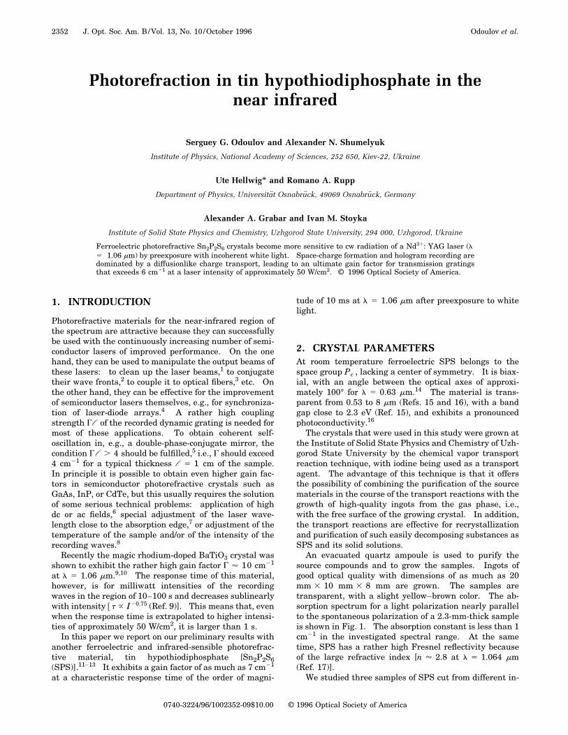
Preexposure should be long enough to reach the largestpossible value of the index modulation (gain factor).After preexposure the sample remains sensitized for acomparatively long time. The next figures show how thegain factor becomes larger with increasing preexposuretime (Fig. 10) and how it gradually becomes smaller with
Fig. 10. Gain factor Gf (with geometric correction) versus preex-posure time.
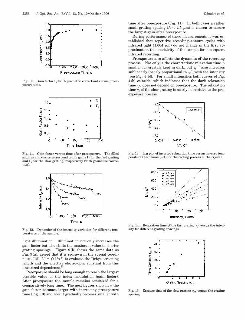
Fig. 11. Gain factor versus time after preexposure. The filledsquares and circles correspond to the gains Gf for the fast gratingand Gs for the slow grating, respectively (with geometric correc-tion).
Fig. 12. Dynamics of the intensity variation for different tem-peratures of the sample.
time after preexposure (Fig. 11). In both cases a rathersmall grating spacing (L , 2.5 mm) is chosen to ensurethe largest gain after preexposure.During performance of these measurements it was es-
tablished that repetitive recording–erasure cycles withinfrared light (1.064 mm) do not change in the first ap-proximation the sensitivity of the sample for subsequentinfrared recording.Preexposure also affects the dynamics of the recording
process. Not only is the characteristic relaxation time tfsmaller for crystals kept in dark, but tf
21 also increasessublinearly (nearly proportional to AI) with the intensity[see Fig. 4 (b)]. For small intensities both curves of Fig.4 (b) coincide, which indicates that the dark relaxationtime tfd does not depend on preexposure. The relaxationtime ts of the slow grating is nearly insensitive to the pre-exposure process.
Fig. 13. Log plot of inverted relaxation time versus inverse tem-perature (Arrhenius plot) for the cooling process of the crystal.
Fig. 14. Relaxation time of the fast grating t f versus the inten-sity for different grating spacings.
Fig. 15. Erasure time of the slow grating t2E versus the gratingspacing.

Odoulov et al. Vol. 13, No. 10 /October 1996 /J. Opt. Soc. Am. B 2357
E. Recording at Reduced TemperatureTo suppress the slow grating (and probably to eliminateit) we studied beam coupling at temperatures below am-bient temperature. The sample is mounted on a holderof a Peltier element of a microcooler, permitting reductionof the temperature down to 215 °C. Figure 12 shows thedynamics of the intensity variation (similar to that shownin Fig. 3) for three different temperatures. It is obviousthat, when the temperature becomes smaller, the relax-ation time of the slow grating increases, and its ampli-tude decreases.Within the relatively narrow temperature interval
(210 to 20 °C) investigated here, the variation of the re-laxation time with temperature can be approximated byan exponential law (Fig. 13). Between cooling and sub-sequent heating of the sample back to ambient tempera-ture we found a thermal hysteresis to occur.
F. Relaxation ProcessesSeveral relaxation times characterize the described pro-cesses of grating recording and erasure: tf , recordingtime of the fast grating; tfd , relaxation time of the fastgrating in the dark; ts , formation time of the slow grating(which is the same with and without light); te , lifetime ofcarriers populating shallow electron traps, i.e., lifetime ofthe sensitized state; tsE , erasure time of the slow grating,etc.As for other photorefractive crystals, the nonzero con-
ductivity results in a relaxation of the grating, and thegrating time is always proportional to a certain dielectricrelaxation time. Some modifications can appear, how-ever, if the characteristic charge-transport lengths be-come comparable with the grating spacing. In thesecases the behavior of t 5 t (L) can be used for evaluationof relevant transport lengths.We measured the dependences of tf and tsE on the grat-
ing spacing L. The data for sample 1 preexposed towhite light are shown in Figs. 14 and 15. The significantvariation of the characteristic time within the measuredinterval of spacings between 1 and 6 mm indicates that itis not only the dielectric relaxation time that defines therelaxation processes.
4. DISCUSSIONAll the data described above suggest the conclusion thatdiffusion is the main process of charge redistribution forthe studied crystals during the formation of the fast grat-ing. The presence of a unidirectional intensity transferbetween the recording waves in beam-coupling experi-ments, with the direction depending on the orientation ofthe ferroelectric axis (Fig. 3; see also Fig. 3 in Ref. 13),and the inverse dependence of the gain factor on the grat-ing spacing (Figs. 6 and 9) are in favor of this conclusion.However, from these dependences only, we cannot decidewhether the space-charge formation occurs as a result ofband transport24 or charge hopping.25 We return to thisquestion further below in this section. What is impor-tant to state here is that the fast grating is built up by alight-induced charge redistribution and that the charac-teristic time tf of this buildup thus depends on the inten-sity.
The slow grating compensating the fast grating is dis-tinct from the latter and is most probably formed by ther-mally excited movable species (see Figs. 12 and 13). Itscharacteristic time ts is much larger than tf and is inde-pendent of the light intensity. It seems that a certainamount of thermally excited charged particles can moveto compensate the space-charge field of the fast grating bycreating an antiphase grating of space charges localizedon different trap centers.According to a calculation given in Ref. 22 the dynam-
ics of beam coupling can be represented in the form of Eq.(1) for two strongly different relaxation times, ts @ t f .This justifies the procedure of evaluation of the relaxationtimes, tf and ts , described in Subsection 3.B.If the slow grating is formed by thermally activated
charge motion, this grating can be strongly suppressed bya decrease in the temperature of the sample, a fact thatagrees with our observations described in Subsection 3.E.From the Arrhenius plot for the characteristic builduptime ts of the slow grating versus reciprocal temperature(Fig. 13) we can estimate the characteristic energy DE forthermal motion of the carriers forming the slow grating.Note that the measured value of DE depends on the di-rection of temperature variation; we obtain DE 5 0.46 0.02 eV when cooling the sample and DE 5 0.36 0.02 eV when heating it back to ambient temperature.Thus a thermal hysteresis exists: After one cooling–heating cycle the relaxation time ts becomes larger andstays that size for a certain time (about 1 month).Next, we further discuss the picture of transitions and
charge transport in SPS crystals (see Fig. 16). We as-sume that there exist deep donor centers in the forbiddenband gap, which are nearly completely filled with elec-trons Ned .
26 There are also shallower centers only par-tially filled with electrons. Being in deep centers, theelectrons are localized in space. Coming to shallow cen-ters, they can jump to adjacent empty centers Nes , thusmoving in space even without light in the sample.The quantum energy of near-infrared radiation used
for recording (hn ' 1.15 eV ) is still insufficient to excitethe electron from the shallow center to the conductionband but increases the probability of hopping with the in-tensity of infrared light; i.e., hopping photoconductivityoccurs.A similar structure of centers exists near the top of the
valence band: deep centers nearly completely filled withholes and shallower centers Nhs (closer to the valenceband) only partially populated by holes. As distinct fromthe shallow electron centers, no light-stimulated hopping,but only thermally activated hopping, is allowed for shal-low hole centers.The process of recording in virgin crystals and in crys-
tals preexposed to white light can be explained as follows.If the sample is kept for a long time (nearly 1 month ormore) in the dark, only a relatively small part of shallowelectron centers are thermally populated. Without infra-red light any nonuniform distribution of charges in shal-low electron levels is self-decaying because of thermalcharge hopping with a decay rate characterized by thetime tfd ' 2 s (see Fig. 4 for tf at I → 0).Light-induced hopping becomes important under illu-
mination with a fringe pattern of infrared light. The

2358 J. Opt. Soc. Am. B/Vol. 13, No. 10 /October 1996 Odoulov et al.
nonuniform space-charge pattern develops because of thelarger rate of hopping in the bright regions of the fringes.The arising index grating is p /2 out of phase with respectto the fringes,25 as in the case of the diffusion band-transport process, and one of the two waves gains inten-sity at the expense of the intensity of the other wave.The dependence of the gain factor G on fringe spacing L isalso similar to that for a diffusion process25:
G 5 ~4p 2n3reffkBT/lLe cos u!@1 1 ~ l S /2pL!2#21.(2)
Here n is the refractive index; reff , the effective electro-optic constant for the particular cut of the crystal used inthis experiment; kBT, the thermal energy; T, the absolutetemperature; l, the laser wavelength; e, the electroncharge; u, the crossing half-angle of the incident waves in-side the sample; and l S , the Debye screening length.From the linearized dependence shown in Fig. 9(b)(cos u ' 1 for sufficiently large L):
~1/GL cos u! 5 ~le/4p 2n3reffkBT !@1 1 ~ l S/2pL!2#,(3)
it is possible to evaluate the Debye screening length27
l S 5 ~««0kBT/e2NR!1/2, (4)
where NR is the effective trap concentration. For theconsidered subsystem responsible for the fast grating, wehave NR 5 (Ne
2 Ne1 )/Ne
0.For the sample without preillumination the density of
filled shallow levels Ne2 is much smaller than the total
density Ne0 of these levels. The Debye screening length
is limited in this case by the number of filled centersNe
2 and not by the number of empty traps Ne1, as hap-
pens quite often in sillenite-type28 or in BaTiO3crystals.25,29 This density can be evaluated from thedata shown in Fig. 9 with « ' 230 (Ref. 30) to beNe
2 ' 7.3 3 1014 cm23.When the crystal is preilluminated by white light, a
part of the electrons of the deep donor centers populatethe shallow centers by means of the conduction band, in-creasing Ne
2. Indeed, after preillumination the gain fac-tor increases, and the maximum of the gain factor movesto smaller L (see Fig. 9), thus indicating the decrease ofthe Debye screening length and the increase of the donordensity to Ne
2 5 7.7 3 1015 cm23. The lifetime of theshallow centers is rather long; therefore they can be popu-lated even with relatively low-power sources of whitelight, such as halogen lamps.
Fig. 16. Scheme of electron transitions and energy levels.
From the intersection point of the straight lines in Fig.9(b) with the OY axis, the value of the efficient electro-optic constant can be extracted by
reff 5 ~le/4p 2n3kBT !/~1/GL cos u!, (5)
with the denominator being taken at (1/L2) 5 0. Notethat two intensity dependences intersect the OY axis inthe same point, thus indicating, as can be expected, thatthe effective electro-optic constant is not affected by illu-mination. The estimated values of the electro-optic con-stant are reff 5 36.5 pm/V and reff 5 53 pm/V for samples1 and 3, respectively. This difference in reff values fortwo samples cut in a similar way may indicate the pres-ence of 180° domains, with an antiparallel orientation ofspontaneous polarization in sample 1.The excess population of the shallow electron levels is
metastable and decays with time. With decreasing den-sity of filled shallow levels Ne
2 the Debye screeninglength becomes larger, and the dependence G 5 G(L), la-beled 1 in Fig. 9(a), is gradually transformed into the de-pendence labeled 2. If we measure the value of the gainfactor at a small grating spacing, e.g., at L 5 1 mm, weobserve a smooth decrease of G with time, as is shown inFig. 11. Fitting the curve of Fig. 11 to exp(2t/te), we canobtain as a rough estimate for the lifetime of electrons onthe shallow levels te ' 36 h.As has already been mentioned above, the band-
transport model qualitatively predicts the same results asthe hopping model for almost all the experimental depen-dences. Fortunately, there is one prediction that is dif-ferent in these models, and it allows us to differentiatethem. According to the band-transport model, the ab-sorption of infrared quanta creates free carriers in theconduction band. These carriers can be retrapped by thesame or similar shallow centers, but they can also be cap-tured by deep donor centers from which they have beenreleased by preexposure with white light. Therefore, in aband-transport model, any exposure to infrared lightmust result in a decrease of density of the filled shallowcenters Ne
2 and in a gradual loss of sensitivity to subse-quent infrared recording.In a hopping model, in contrast, there is no excitation
of free carriers to the conduction band, and the infraredlight cannot stimulate the decay of excitations from shal-low centers to deep donor centers. So infrared recording(and infrared erasure) does not change the density Ne
2
and therefore does not affect the sensitized state, inagreement with our results.Finally, we discuss the evaluation of the characteristic
transport lengths for SPS at ambient conditions from thedynamics of recording and erasure. The theory (see, e.g.,Refs. 27, 28, and 31) relates the relaxation time t of anisolated grating (fast or slow) to the dark dielectric relax-ation time tdi , the Debye screening length l S , and thediffusion length l D , as follows:
t 5 tdi@1 1 ~Kl D!2#/@1 1 ~Kl S!2#@1 1 ~kI/sd!#, (6)
where k is the specific photoconductivity and sd is thedark conductivity.Because the fast grating is recorded by photoexcited
carriers and the slow one by thermally excited carriers,we treat them separately. For large intensity in the case
Odoulov et al. Vol. 13, No. 10 /October 1996 /J. Opt. Soc. Am. B 2359
of the fast grating the unity can be omitted in the lastterm of the denominator of Eq. (6), and this relation canbe rewritten as
t f I 5 ~««0 /k!@1 1 ~Kl De!2#/@1 1 ~Kl S
e!2#. (7)
First, this relation says that all the dependences t f5 t f (K) measured at different intensities should coin-
Fig. 17. Dependence of the product (It f)21 on the grating spa-
tial frequency K.
Fig. 18. Erasure time of the slow grating tsE versus the gratingspatial frequency.
Fig. 19. Interaction area of the beam inside the crystal: l ,crystal thickness; u i , angle of incidence inside the crystal; 2x,beam diameter at the height y(x) of the beam cross section.
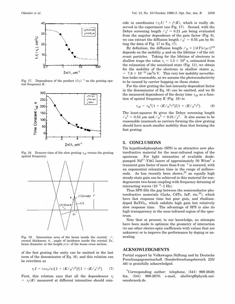
cide in coordinates (t f I)21 5 f (K), which is really ob-
served in the experiment (see Fig. 17). Second, with theDebye screening length l S
e ' 0.21 mm being evaluatedfrom the angular dependence of the gain factor (Fig. 6),we can extract the diffusion length l D
e ' 0.55 mm by fit-ting the data of Fig. 17 to Eq. (7).By definition, the diffusion length l D 5 @(kT/e)mt#1/2
depends on the mobility m and on the lifetime t of the rel-evant particles. Taking for the lifetime of electrons inshallow traps the value te ' 1.5 3 105 s, estimated fromthe relaxation of the sensitized state (Fig. 11), we obtainfor the mobility of the electrons in shallow states me' 7.8 3 10213 cm2/s V. This very low mobility neverthe-less looks reasonable, as we assume the photoconductivityto be caused by carrier hopping on these states.For the slow grating the last intensity-dependent factor
in the denominator of Eq. (6) can be omitted, and we fitthe measured dependence of the decay time tsE as a func-tion of spatial frequency K (Fig. 18) to
tsE 5 tdih@1 1 ~Kl D
h!2#/@1 1 ~Kl Sh!2#. (8)
The least-squares fit gives the Debye screening lengthl S
h ' 0.53 mm and l Dh , 0.01 l S
h. It also seems to bereasonable inasmuch as carriers forming the slow gratingshould have much smaller mobility than that forming thefast grating.
5. CONCLUSIONSTin hypothiodiphosphate (SPS) is an attractive new pho-torefractive material for the near-infrared region of thespectrum. For light intensities of available diode-pumped Nd31:YAG lasers of approximately 50 W/cm2 atransient gain factor of more than 6 cm21 is ensured, withan exponential relaxation time in the range of millisec-onds. As has recently been shown,32 an equally highsteady-state gain can be achieved in this material for non-degenerate two-beam coupling with frequency detuning ofinteracting waves (1022–1 Hz).Thus SPS fills the gap between the semiconductor pho-
torefractive materials (GaAs, CdTe, InP, etc.33), whichhave fast response time but poor gain, and rhodium-doped BaTiO3, which exhibits high gain but relativelyslow response time. The advantage of SPS is also itshigh transparency in the near-infrared region of the spec-trum.Note that at present, to our knowledge, no attempts
have been made to optimize the geometry of interaction(to use other electro-optic coefficients with values that areunknown) or to improve the performance by doping or an-nealing.
ACKNOWLEDGMENTSPartial support by Volkswagen Stiftung and by DeutscheForschungsgemeinschaft (Sonderforschungsbereich 225/A6) is gratefully acknowledged.
*Corresponding author: telephone, (541) 969-2649;fax, (541) 969-2670; e-mail, [email protected].

2360 J. Opt. Soc. Am. B/Vol. 13, No. 10 /October 1996 Odoulov et al.
APPENDIX A: INTERACTION LENGTHAs shown in Fig. 19, the total area of a beam inside thecrystal is A0 5 l 2x/cos u i [l denotes the crystal thick-ness; 2x, the beam diameter at the height y(x) of thebeam cross section; and ui , the angle of incidence insidethe crystal]. The interaction area of both beams insidethe crystal is AWW 5 A0 2 (l 2/2)tan ui . The quantityc(x) 5 AWW /A0 5 1 2 (l /4 x)sin u i defines the correc-tion factor as a function of x. By integrating c(x) overthe whole diameter of the beams D and by taking into ac-count the refraction law sin ui 5 sin ue /n (with n beingthe refractive index and ue the angle of incidence in air),we obtain the total correction factor 1 2 pl sin ue /4nDfor the interaction length; i.e., the crystal thickness l hasto be replaced by the effective interaction length l eff5 l (1 2 pl sin ue /4nD).
REFERENCES AND NOTES1. S. K. Kwong and A. Yariv, ‘‘One-way, real time wave front
converters,’’ Appl. Phys. Lett. 48, 564–566 (1986).2. M. Cronin-Golomb, J. Paslaski, and A. Yariv, ‘‘Vibration re-
sistance, short coherence length operation, and mode-locked pumping in passive phase conjugate mirrors,’’ Appl.Phys. Lett. 47, 1131–1133 (1985).
3. S. Weiss, M. Segev, S. Sternklar, and B. Fischer, ‘‘Photore-fractive dynamic optical interconnects,’’ Appl. Opt. 27,3422–3427 (1988).
4. S. MacCormack and R. W. Eason, ‘‘Efficient amplification ofa single-mode laser diode by photorefractive beam combina-tion using an injection-locked diode-laser array pump,’’ Opt.Lett. 15, 1212–1214 (1990).
5. S. K. Kwong, M. Cronin-Golomb, and A. Yariv, ‘‘Oscillationwith photorefractive gain,’’ IEEE J. Quantum Electron. 22,1508–1523 (1986).
6. M. B. Klein, S. W. McCahon, T. F. Boggess, and G. C. Val-ley, ‘‘High-accuracy, high-reflectivity phase conjugation at1.06 mm by four-wave mixing in photorefractive gallium ar-senide,’’ J. Opt. Soc. Am. B 5, 2467–2472 (1988).
7. J. E. Millerd, S. D. Koehler, E. M. Garmire, A. Partovi, A.M. Glass, and M. B. Klein, ‘‘Photorefractive gain enhance-ment in InP:Fe using band-edge resonance and tempera-ture stabilization,’’ Appl. Phys. Lett. 57, 2776–2778 (1991).
8. G. Picoli, P. Gravey, C. Ozkul, and V. Vieux, ‘‘Theory of two-wave-mixing gain enhancement in photorefractive In-P:Fe: a new mechanism of resonance,’’ J. Appl. Phys. 66,3798–3813 (1989).
9. G. W. Ross, P. Hribek, R. W. Eason, M. H. Garret, and D.Rytz, ‘‘Impurity enhanced self-pumped phase conjugationin the near infrared in ‘blue’ BaTiO3 ,’’ Opt. Commun. 101,60–64 (1993).
10. B. A. Wechsler, M. B. Klein, C. C. Nelson, and R. N.Schwartz, ‘‘Spectroscopic and photorefractive properties ofinfrared-sensitive rhodium-doped barium titanate,’’ Opt.Lett. 19, 536–538 (1994).
11. A. A. Grabar, R. I. Muzhikash, A. D. Kostyuk, and Yu. M.Vysochanskiy, ‘‘Investigation of the switching process inthe domain structure of ferroelectric Sn2P2S6 by the dy-namic holographic method,’’ Sov. Phys. Solid State 33,1314–1316 (1991).
12. A. A. Grabar, Yu. M. Vysochanskiy, I. M. Stoyka, M. M.Danko, and V. Yu. Slivka, ‘‘Influence of the domain struc-ture on photorefractive properties of a ferroelectricSn2P2S6 ,’’ Ukr. Phys. J. 39, 941–942 (1994).
13. A. N. Shumelyuk, U. Hellwig, R. A. Rupp, S. G. Odoulov,and A. A. Grabar, ‘‘Infrared recording in photorefractive
tin-hypothiodiphosphate (Sn2P2S6),’’ in Photorefractive Ma-terials, Effects, and Devices Topical Meeting (Optical Soci-ety of America, Washington, D.C., 1995), pp. 80–83.
14. A. A. Grabar, Y. M. Vysochanskiy, S. I. Perechinskii, L. A.Salo, M. I. Gurzan, and V. Yu. Slivka, ‘‘Thermooptic inves-tigations of ferroelectric Sn2P2S6 ,’’ Sov. Phys. Solid State26, 2087–2089 (1984).
15. C. D. Carpentier and R. Nitsche, ‘‘Vapour growth and crys-tal data of the thio(seleno)-hypodiphosphates Sn2P2S6 ,Sn2P2Se6 , Pb2P2S6 , Pb2P2Se6 and their mixed crystals,’’Mater. Res. Bull. 9, 401–410 (1974).
16. M. I. Gurzan, A. P. Buturlakin, V. S. Gerasimenko, N. F.Korda, and V. Yu. Slivka, ‘‘Optical properties of Sn2P2S6crystals,’’ Sov. Phys. Solid State 19, 1794–1795 (1977).
17. Yu. M. Vysochanskiy and V. Yu. Slivka, Ferroelectrics of theSn2P2S6 Family. Properties in the Vicinity of the LifshitsPoint, 1st ed. (Scientific Edition, L’vov, 1994), Chap. 10, p.244 (in Russian).
18. G. Dittmar and H. Schaefer, ‘‘The crystal structure ofSn2P2S6 ,’’ Z. Naturforsch. 29b, 312–317 (1974).
19. C. D. Carpentier and R. Nitsche, ‘‘Ferroelectricity inSn2P2S6 ,’’ Mater. Res. Bull. 9, 1097–1100 (1974).
20. G. A. Brost, R. A. Motes, and J. R. Rotge, ‘‘Intensity-dependent absorption and photorefractive effects in bariumtitanate,’’ J. Opt. Soc. Am. B 5, 1879–1885 (1988).
21. R. L. Townsend and J. T. LaMacchia, ‘‘Optically induced re-fractive index changes in BaTiO3 ,’’ J. Appl. Phys. 41, 5188–5192 (1970).
22. S. Zhivkova and M. Miteva, ‘‘Holographic recording in pho-torefractive crystals with simultaneous electron–holetransport and two active centers,’’ J. Appl. Phys. 68, 3099–3103 (1990).
23. M. B. Klein and G. C. Valley, ‘‘Beam coupling in BaTiO3 at442 nm,’’ J. Appl. Phys. 57, 4901–4905 (1987).
24. N. Kukhtarev, V. Markov, S. Odoulov, M. Soskin, and V. Vi-netskii, ‘‘Holographic storage in electrooptic crystals,’’ Fer-roelectrics 22, 949–964 (1979).
25. J. Feinberg, D. Heiman, A. R. Tanguay, and R. W. Hell-warth, ‘‘Photorefractive effects and light-induced chargemigration in barium titanate,’’ J. Appl. Phys. 51, 1297–1305 (1980).
26. Until now the signs of movable charges responsible for thefast and the slow gratings were not established. The attri-bution of the fast component to electrons and of the slowcomponent to holes still has to be proved by independentexperiments.
27. S. I. Stepanov and M. P. Petrov, in Photorefractive Materi-als and Their Applications I, P. Gunter and J.-P. Huignard,eds., Vol. 62 of Topics in Applied Physics (Springer-Verlag,Berlin, 1988), p. 263.
28. M. P. Petrov, S. J. Stepanov, A. V. Khomenko, Photorefrac-tive Crystals in Coherent Optical Systems, Vol. 59 of OpticalSciences (Springer-Verlag, Berlin, 1991).
29. M. B. Klein, in Photorefractive Materials and Their Appli-cations I, P. Gunter and J.-P. Huignard, eds., Vol. 61 of Top-ics in Applied Physics (Springer-Verlag, Berlin, 1988), p.195.
30. A. A. Volkov, G. V. Kozlov, N. I. Afanasieva, Yu. M. Vysoch-anskiy, A. A. Grabar, and V. Yu. Slivka, ‘‘Low-frequencymodes in the infrared spectrum of an Sn2P2S6 crystal,’’ Sov.Phys. Solid State 25, 1482–1483 (1983).
31. N. Kukhtarev, ‘‘Kinetics of hologram recording and erasurein electrooptic crystals,’’ Sov. Tech. Phys. Lett. 2, 438–440(1976).
32. S. G. Odoulov, A. N. Shumelyuk, G. A. Brost, and K. M.Magde, ‘‘Enhancement of beam coupling in near infraredfor tin hypothiodiphosphate,’’ Appl. Phys. Lett. (to be pub-lished).
33. A. M. Glass and J. Strait, in Photorefractive Materials andTheir Applications I, P. Gunter and J.-P. Huignard, eds.,Vol. 61 of Topics in Applied Physics (Springer-Verlag, Ber-lin, 1988), p. 237.