philips resear~ repor ~:~~~i · pdf file · 2014-01-09impatt-diode oscillator,...
TRANSCRIPT

--------~ -
PHILIPSRES EAR ~___"REPOR ~:~~~I
SUPPLEMENTS
,
PHlllPS RESEARCH LABORATORIES I
hllips Res. Repts Suppl. 1973 No.7
ted In the Netherlllnd5
<Cl N.V. Philips' Gloeilampenfabrieken, Eindhoven, Netherlands, 1973.Articles or illustrations reproduced, in whole or in part, must be
accompanied by full acknowledgement of the source:PHILlPS RESEARCH REPORTS SUPPLEMENTS

•
NOISEIN IMPATT-DIODE OSCILLATORS *)
BY
J. J. GOEDBLOED
*) Thesis, Technological University Eindhoven, November 1973.Promotor: Prof. Dr H. Groendijk.
Philips Res. Repts Suppl. 1973, No. 7.
AbstractThis paper deals with noise in singly tuned, low-loaded-Q IMPATT-diode oscillators. This noise is caused by the statistical fluctuationsof the thermal generation and impact ionisation processes. The r.f.components of these fluctuations cause so-called "intrinsic" oscillatornoise. Analytical relationships are derived for the intrinsic FM andAM noise for low-level operation of the oscillator. These expressionscontain parameters which can all be derived from independent measure-ments. The theoretical results are in agreement with the measured AMand FM noise data, using Sip+-n, Si n+-p, Ge n+-p and n-GaAsSchottky-barrier diodes. We have discussed how intrinsic oscillatornoise can be reduced by a proper choice of device parameters. Forincreasing signal levels the measured intrinsic FM and AM noise in-creases over the noise predicted by the theory for low signal levels.Furthermore, the ratio of the AM and FM noise is correctly describedby this theory at all signal levels. Within the range of validity of thediode model used, it is concluded that the increase of noise with sig-nallevel is due to the dependence of the noise-generating mechanism onthe signal. A comparison is made with some existing large-signal noisetheories. The low-frequency components of the statistical fluctuationsmentioned give rise to up-converted AM noise predominantly. Ananalytical expression is derived for this type of noise and confirmedexperimentally. Finally the down-conversion of oscillator noise intobias-current noise appears to be negligible within the range of validityof the diode model used.

CONTENTS
I.INTRODUCTION
2. IMPATT-DIODE MODEL 42.1. Introduetion 42.2. The avalanche region . 62.3. The drift region .. . 122.4. Summary of assumptions in the IMPATT-diode model 12
3. THEORY OF THE NOISE-FREE IMPATT DIODE 143.1. Small-signal theory 14
3.1.1. Small-signal impedance . . . . . . . 143.1.2. Diode-quantity analysis; tan cp method 173.1.3. Experimental results .... 203.1.4. Extension of the diode model 213.1.5. Discussion 26
3.2. Large-signal theory 293.2.1. Large-signal impedance 303.2.2. Oscillation condition . 313.2.3. Range of validity of the noise-free large-signal model
(RVM) . . . . . . . . . . . . . 333.2.4. Microwave impedance measurements 373.2.5. D.e. restorage 38
4. NOISE OF THE NON-OSCILLATING DIODE 434.1. Introduetion of the noise source . . . . 444.2. The total noise current . . . . . . . . 454.3. Extension of the diode model; discussion 474.4. R.f. noise measurements 494.5. L.f. noise measurements 53
5. OSCILLATOR NOISE 565.1. Introduetion 565.2. Experimental arrangement 605.3. General oscillator-noise theory 665.4. Application of the general oscillator-noise theory to IMPATT-
diode oscillators 695.4.1. Summary of diode and circuit parameters . . . . 705.4.2. The ratio of the intrinsic AM to FM noise power' 725.4.3. Up-converted and down-converted oscillator noise 76

6. LINEAR THEORY OF IMPATT-DIODE-OSCILLATOR NOISE 796.1. Introduetion 796.2. Width and form of the output spectrum 806.3. Intrinsic FM oscillator noise 876.4. Intrinsic AM oscillator noise , . 916.5. Reduction of intrinsic oscillator noise 93
7. NON-LINEAR IMPATT-DIODE-OSCILLATOR NOISE 1027.1. Introduetion 1027.2. Modulation noise 1027.3. Excess noise 108
7.3.1. Discussion 109
REFERENCES 114

-1-
1. INTRODUCTION
In March 1958 W. T. Read Jr., in his paper "A proposed high-frequencynegative-resistance diode"1) put forward the suggestion that it should bepossible to construct a microwave oscillator in which the active device is asemiconductor diode under breakdown conditions. In February 1965 the firstexperimental realisation of Read's proposal was reported by Johnston, DeLoachand Cohen")"). Since 1965 a large number of studies has been put forward con-cerning the excitation of microwaves using an avalanching diode, i.e. a diodeunder breakdown in which, due to impact-ionisation processes, an avalancheof charge carriers is created.The operation of a microwave oscillator with avalanche diode is based on the
fact that for certain conditions this diode shows an impedance with a negativereal part. With the aid of this negative resistance the loss resistance of anoscillator loop can be cancelled out, thus making oscillations possible. Thenegative resistance is partly due to the nature of the avalanche process andpartly due to transit-time effects. These two origins explain the designationIMPATT-diode oscillator, where the acronym IMPATT stands for IMPact-ionisation, Avalanche and Transit-Time. The avalanche process turns out tobe an inductive process, thus giving rise to a 90° phase shift between voltageand current. The additional phase shift needed to arrive at an impedance with,a negative real part, is obtained by a phase delay due to the transit time of thecarriers through the junction.The practical application of an IMPATT-diode oscillator depends to a large
extent on the noise characteristics of this oscillator. Hence soon after theoscillator became operational the first measurements of noise in these oscil-lators were already reported 4.5). A large number of theoretical and experimen-tal studies ofnoise in IMPATT diodes and IMPATT-diode oscillators followed.An excellent review of these studies, up to May 1971, has been presented byGupta 6). When reading the part of his review on noise in IMPATT-diodeoscillators it strikes one that the number of papers is very limited in which thenoise in these oscillators is discussed starting from the physical properties ofthe diode itself. Furthermore, a detailed experimental check of these theoriesis lacking.The first theory of noise in IMPATT-diode oscillators has been presented by
Hines 7). His analysis, which he considers as a first approximation only, isbased upon results of his small-signal analysis for IMPATT-diode amplifiers B).The first large-signal theory for noise in IMPATT-diode oscillators was pub-
*) From a paper by Val'd-Perlov, Tager and Krasilov 3) dated November 1966 it can be con-cluded that they had already realised Read's proposal in 1959.

-2-
lished by Inkson 9). He used the sharp-pulse approximation, already suggestedby Read 1), to describe the conduction current leaving the region of the junctionwhere the impact ionisation takes place. This means that his theory is applicableto high-level operating oscillators only.Vlaardingerbroek 10) put forward an analytical theory which provides
expressions for the output-power spectrum and the width of the output spec-trum for IMPATT-diode oscillators operating at Iow signal levels, This theory,which is based on the fact that the output signalof an oscillating loop consistsof narrow-band amplified noise, has been worked out in more detail by Vlaar-dingerbroek and the present author in ref. 9. In that paper the influence of low-frequency noise on the oscillator noise was also discussed. The paper in ques-tion formed the basis ofthe present study, in which we shall try to describe thenoise in IMPATT-diode oscillators in terms of physical properties and dimen-sions of the diode itself. For this reason the circuits used were singly tuned andhad a low-loaded quality factor of the cavity, so that the oscillator noise isaffected as little as possible by the circuit.The thesis is arranged as follows.In chapter 2 the diode model used is introduced. This model is of great
importance as we want to describe the oscillator noise analytically starting fromthe processes which take place inside the diode.Chapter 3 deals with the small-signal and the large-signal behaviour of the
noise-free IMPATT diode. The small-signal behaviour ofthe diode is of impor-tance as it enables us to determine the value of several diode parameters. Astudy of the noise-free oscillator is of great interest because if the quasi-stationary quantities like output power and large-signal impedance cannot bedescribed by the diode model used, we can have no illusions about the descrip-tion of the oscillator noise using the same diode model.In chapter 4 the noise of the non-oscillating diode is discussed. Special
attention is paid to the intrinsic response time of the avalanche process whichgoverns the internal noise properties of the diode.Chapter 5 summarises briefly the general theory of oscillator noise which, in
principal, is applicable to any oscillator, and it is applied to the special case ofIMPATT-diode-oscillator noise. Furthermore, the oscillator-noise-measuringequipment is described.In chapter 6 the basic idea that the output signal consists of narrow-band
amplified noise is worked out and checked in detail experimentally. The theorypresented is restricted to low signal levels so that the output power can be as-sumed mainly as linearly amplified noise, the only non-linearity taken intoaccount being the determination of the output power level, as described inchapter 3.
Chapter 7 finally deals with up-converted and down-converted noise, i.e.with oscillator noise caused by low-frequency noise and the reverse. Further-

-3-
more, the deviations between the oscillator noise found experimentally and thenoise predicted by the linear noise theory of chapter 6 are discussed. A com-parison is made with recent theories 13-17) in which the signallevel is notrestricted to low values.

-4-
2. IMPATT-DIODE MODEL
2.1. Introduetion
Since the ultimate aim of the present study is to describe the noise of theIMPATT-diode oscillator, starting from the processes which take place insidethe diode, the diode model to be used is of importance. Before this model isdiscussed in detail, some introductory observations will be made concerningthe diode behaviour under reverse-bias and breakdown conditions 18).
Let us consider a semiconductor diode, e.g. an abrupt p+-n diode, where thesuperscript + denotes material which is heavily doped compared to theadjacent material. There is an electric field across the metallurgical junction ofthe diode 19). The magnitude of this field can be increased by applying a reversebias voltage to the diode. For the present diode this means that a positive volt-age is applied to the n-type materialof the junction with respect to the p-typematerial. The layer in which the electric field is present is almost depleted offree carriers and is therefore called the depletion layer. The very small current(a few nano-amperes) which is still flowing through this layer is called thesaturation current. This current is carried by electrons and holes generatedthermally in the semiconductor material.
When an electron-hole pair is generated within the depletion layer it will besplit immediately owing to the presence of the electric field. The electron movestowards the n-region, and the hole towards the p-region. Both carriers movewith their corresponding drift velocity, which is defined as the average velocitycomponent of the carrier parallel to the electric field. The velocity componentis averaged over a time interval which is long compared to the average timebetween two collisions of the carrier with the crystallattice.
At low values of the electric field the drift velocity increases with increasingfield. For high values of the field the drift velocity more or less saturates. Forelectrons in silicon, for example, the drift velocity becomes saturated for fieldvalues larger than 20 kV/cm 20).
Although the drift velocity saturates with increasing field, the kinetic energyacquired in the field by a carrier keeps increasing. If the electric field is highenough, a carrier can acquire so much energy that it will be able to ionise alattice atom by impact, thus leading to the creation of an electron-hole pair 21).The electron and hole of this pair, which are separated immediately, can inturn also ionise lattice atoms and create new electron-hole pairs, and so on.This process is called the avalanche process. It can give rise to large reversecurrents and this phenomenon is known as junction breakdown. The capabilityfor impact ionisation can be expressed by an ionisation coefficient, generallydenoted by ct for electrons and (3 for holes 22). The ionisation coefficient givesthe average number of electron-hole pairs created by one carrier per unit length

-5-
n a direction parallel to the electric field. From experiments 23) and from atheory by Shockley 24) it is known that o: and (3 can be expressed by
a, (3 = a exp (-biE)"',
where a, b and m are constants and E the magnitude of the electric field (m = 1for silicon and germanium, and 2 for gallium arsenide 22». The appearance ofthe exponential function in eq. (2.1) can be readily understood. If BI is theenergy needed to ionise a lattice atom, then the carrier which ionises this atomby impact must have at least this energy in order to do so. A carrier has anenergy BI when it has travelled a distance 11given by q 11E = BI' where q is theelectronic charge. Let I be the average distance between two (non-ionising)collisions of the carrier with the lattice. Then the probability that the carriertravels the distance 11 without a collision is proportional to
(Bt/q I)exp (-/t/l) = exp - e- .
It will be clear that the ionisation coefficient is proportional to this function.Owing to the field dependence of rx and (3 impact ionisation (or avalanche
multiplication) generally occurs in a relatively narrow region of the depletionlayer, namely the region with the highest values of the electric field. This regionis generally called the avalanche region. The remaining part of the depletionlayer is called the drift region, since the carriers only drift through it. In mostpractical situations it can be assumed that the carriers travel at saturated driftvelocity throughout the depletion layer.
Since the carriers generated in the avalanche region reduce the electric fieldin that region once they have drifted out of the avalanche region, a steady-avalanche process is generally possible. In this steady avalanche the rate ofionisation is such that the mean number of electron-hole pairs created by aninitial pair is unity if the number of thermally generated electron-hole pairs isnegligible. When (3 = rx the steady-avalanche condition is 1)
la
J a dx = 1.o
When (3 =F rx, it is 25)
la XJ o: exp [f ((3 - rx) dÇ] dx = 1,o 0
(2.l)
(2.2)
(2.3)
(2.4)

-6-
where la is the length of the avalanche region. Equation (2.4) can be reduced to
0: = (3 exp [(0: - (3) la], (2.5)
when 0: and (3 do not depend on the position (x) in the avalanche region.From the above it will be clear that the avalanche process is highly non-linear.
This fact particularly affects the behaviour of the oscillating diode, not only thequasi-stationary quantities such as impedance and output power but also thefluctuating quantities. The fluctuations, i.e. the noise, are present due to thefact that both the thermal-generation process and the ionisation process arestatistical processes.
All this will be discussed in detail later on in this study. From the introduetiongiven, we derive the principal assumption on which the diode model used isbased, namely:
In an avalanching junction carrier generation by impact ionisation and car-rier drift occur in different regions of the depletion layer: the avalanche regionand the drift region.
The avalanche region will be discussed in sec. 2.2, the drift region in sec. 2.3.In the course of our theoretical and experimental investigations it was foundthat the quantities which interest us can be described on the basis of a relativelysimple diode model. The assumptions regarding this simple diode model aresummarised in sec. 2.4.
2.2. The avalanche region
The avalanche multiplication which takes place in the avalanche region only,will be considered to be uniform over the diode area (one-dimensional problem).Moreover, we confine the analysis to the region of not too high frequencies,where the energy relaxation time and the momentum relaxation time can beneglected compared with the period of oscillation 26). Under these conditions,and in the absence of noise and recombination effects, the kinetic equations forthe electrons and holes are the continuity equations
(2.6)
() 1 ()-p = - - - Jp + 0: 11 Vn + (3p v i»()t q öx (2.7)
where 11 and p are the concentrations of electrons and holes, Jn and Jp theelectron and hole current densities, 0: and (3 the ionisation coefficients of elec-trons and holes, Vn and "» the saturated drift velocities ofthe electrons and holes,and q the electronic charge. All quantities in eqs (2.6) and (2.7) are positive andmay depend (with, of course, the exception of q) on the position coordinate x

-7-
and the time coordinate t. The holes are assumed to drift in the positive x-direction.The fluctuations of the avalanche process can be introduced into the math-
ematical description by adding a noise term to eqs (2.6) and (2.7), so that theseequations take the form of a Langevin equation 27). The noise will be left outof consideration in the present chapter and also in chapter 3. The introduetionof the noise term into the description will be discussed in detail in sec. 4.1.We continue the present section with the derivation of an expression for the
total noise-free conduction current in the avalanche region. This expression,generally called the Read equation, has been the subject of several studies 28- 30).
For this reason we willlimit the derivation of the Read equation to the simpli-fied case where IX = {J, independently of x, and Vn = Vp = v, also independentlyof x. In this way the algebra is kept simple, while the principal assumptions tobe made can still be stated. The Read equation will be subsequently refined toaccount for IX =1= (J and Vn =1= Vp'
Adding eqs (2.6) and (2.7) we find
while subtracting these equations yields
where Je = Jn + Jp, and use has been made of the expressions Jn = q n v andJp = q p v. The expression for the total conduction current leaving the ava-lanche region is found after integration of eq. (2.8) over the length of theavalanche region:
The first term on the right-hand side of this equation can be written
where Jc(O) = Jc(la) is the conduction current at the boundaries of the av-alanche region, and Js = Jps + Jns is the saturation current entering the av-
(2.8)
(2.9)
(2.10)
(2.11)

-8-
alanche region. The second term on the right-hand side of eq. (2.10) can beworked out by means of partial integration. After some straightforward cal-culations, also using eq. (2.9), this yields
According to the mean-value theorem
where Xo is a suitably chosen value of x in the interval Os; x ~ la. For the timederivative of Je in the term on the left-hand side of eq. (2.10) we therefore find
(2.13)
We next assume the angular frequency (w) considered in our studies to be solow that (w la/v)2 = (w 'ia)2 « I ('ia being the transit time of the carriers in theavalanche region). The term containing the second-order time derivative in eq.(2.13) can then be neglected. This means that Je and also J; - Jp can be replacedby their quasi-stationary approximations
and (2.14)J; - Jp = Je(O) (1 - 2 IX x),
which can be obtained from eqs (2.6) and (2.7) with brD! = O. Substitution ofeqs (2.11), (2.12) and (2.14) in eq. (2.10) yields
b'ia (1 + IX la - § 1X21/) - Je(O) =
b!
2 Je(O) [ IX la (1 +i 'ia ()()! IX la) - 1] + 2r; (2.15)
The ionisation coefficient IX depends on the electric field Ea in the avalancheregion. Representing IX in the neighbourhood of the static field strength, Eao,by its Taylor expansion, we obtain
IX la = IX(Eao) la + ( dlX ) Va+ ... = 1+ a' Va + ... , (2.16)dEa Ea=EaO
-9-
where use has been made of the static breakdown condition, eq. (2.3), andVa = eala, ea being the time-dependent part of Ea, and Va the time-dependentpart of the voltage Va across the avalanche region. In writing Va = ea la weassume ea to be independent of x.We next assume that it is sufficient to expand (X up to the first-order field
derivative of (X only. Then substitution of eq. (2.16) in the left-hand side of eq.(2.15) yields
(2.17)
where we have neglected terms containing Va2 and ()va!'bt. If 5 (X' va/2 « 1 eq.(2.17) reduces to the well-known Read equation
(2.18)
In the preceding derivation several rather crude assumptions were made:(1) (W'1:a)2« 1. For w/2n = 10 GHz and v = 105 mis, W'1:a = 0·63 per
micron length of the avalanche region, while 0·6 [.Lm< la < 2·2 [.Lmfor thediodes we investigated (see chapter 3).
(2) Both the second- and higher-order field derivatives as well as the timederivatives of (x' were neglected. In view of the strong field dependence of (X(eq. (2.1)), this also is a questionable assumption. Some of the consequences ofthe second-order field derivative of (X will be discussed in sec. 3.2.
(3) The assumption that 5 (X' va/2 « 1, and our neglect of terms containingv/ and ()Va/()t limit the validity of eq. (2.18) theoretically to rather low valuesof Va' For example (see chapter 4) (x' = 0·3is found from the experimental data.This means that 5 (X'/2 = 0·75.
However, nature is occasionally kind to the investigator. It is found that ifall these three assumptions are made, eq. (2.18) is a good description of theconduction current over a considerable range of frequencies and voltages. Thiswas shown by experiments (sec. 3.2) and is also suggested by results of detailednumerical calculations 31). We will therefore continue to use eq. (2.18) in ourcalculations.The time constant '1:a/3 in eq. (2.18) can be considered as the intrinsic response
time of the avalanche process 29). This can be illustrated as follows. Suppose J,to have a stationary value Jso for t <O.At t = 0, Js rises to a value Jso + LIJs.This causes Je to increase from its stationary value Jco' For small values of t itfollows from eq. (2.18) that the increase is given by
tJe - Jco F:::! - LIJs,
'1:t

-10-
where -Cl = -ca/3 and where we assumed a' Va I/-CI «1. In this simplified example,therefore, it takes -Cl seconds to increase the current Jeo caused by LIJs by anamount LIJs'The intrinsic response time -Cl will prove to be of great importance in the
description ofthe noise behaviour ofthe diode. We therefore give the followingelucidation.
In a steady semiconductor avalanche the average number of electron-holepairs involved is constant. For steady high-current avalanches where the numberof thermally generated carriers is negligible, this means that every electron-holepair leaving the avalanche region due to drift must be replaced by a new paircreated by impact ionisation. During one transit time of the avalanche region,therefore, the average number of electron-hole pairs produced by an initial pairis unity. The intrinsic response time can be considered as the average time afterwhich the initial pair creates the pair which succeeds it. The intrinsic responsetime is thus related to the transit time of the carriers in the avalanche region.It will be clear that the intrinsic response time in particular figures in the noisebehaviour of the avalanche process, since all deviations from the ideal flue-tuation-free situation in which anyone pair produces exactly one new pair aftera fixed time delay of -Cl seconds are noise contributions B). In the avalancheprocess these deviations abound, owing to the statistical character of thisprocess and of the thermal-generation process from which the avalanche buildsitself up. The intrinsic response time will be discussed further in chapter 4.
As shown by several authors 2B.32-34), the unequal ionisation coefficientsand unequal drift velocities of electrons and holes will affect the final value ofthe intrinsic response time. Equation (2.18) can then be written in a generalisedform 34.35):
(2.19)
where le = A Je, Is = A Js, A is the junction area and -Cl is given by 32)
2 ((I( fJ)1/2-Cl = -Ca [((I( + fJ) la - 2],
((I( - fJ)2 la(2.20)
when (I( and fJ are independent of the position in the avalanche region. In eq.(2.20) -Ca is defined by
la ( 1 1)-c =- -+-a 2 VII vp'
(2.21)
and la can be found from the breakdown condition eq. (2.5). In eq. (2.19) a is

-11-
an average ionisation coefficient (averaged over exand fJ), the field derivative ofwhich is well approximated by a relation given by Hulin et al. 36):
(2.22)
Thus far only the conduction current in the avalanche region has beenconsidered. The total current It through that region is given by
(2.23)
where Ca = EA/la is the "cold" capacitance of the avalanche region. In fig. 2.1the currents and voltages of interest in the diode are presented in a vector dia-gram in the complex plane 37). Suppose an alternating voltage Vt is applied tothe avalanching junction. Part of this a.c. voltage (va) appears across the
tlma9inary
VI
ie --Real
z
Fig. 2.1. Vector diagram in which the amplitudes and the phases of the various voltages andcurrents in the diode are represented in connection. The diode impedance Z = v,li,.
avalanche region. The voltage Va causes an a.c. conduction current ie in theavalanche region. It follows from eq. (2.19) that this current has a 90° phaselag with respect to Va. The displacement current Ca (d Va/dl) = j W Ca Va has a90° phase lead with respect to Va' We note that the conduction current and thedisplacement current are in anti-phase, so that for a given value of ie, Va and Cathe total a.c. current it is in phase with or in phase opposition to ie, dependingon the frequency w. It is found that if it and ie are in anti-phase the diode willhave an impedance with a negative real part. The frequency at whichI iel = W Ca Va, and hence it = 0, is called the avalanche frequency. The con-dition for a negative resistance can then be formulated as follows: for a givenie, Va and Ca the frequency of the signal applied must be higher than the av-alanche frequency.

-12-
2.3. The drm region
It is assumed that no impact ionisation takes place in the drift region, so thatthe carriers injected into this region from the avalanche region only drift throughit. Furthermore, it is assumed that the carriers travel at saturated drift velocity.
If the current is injected into the drift region at x = la, it causes an inducedcurrent in the external circuit, the fundamental of which is given by
1 JW (W (x - la) )i1nd = I:; ie exp - j V dx == ifJd ie,
la
(2.24)
where Wis the length ofthe depletion layer and Id = W + l« is the length ofthedrift region. The current i1nd is also the average conduction current in the driftregion (fig. 2.1). The transit-time function ifJd, given by
l-exp (-jO)ifJd = ,
jOW Id
0=-V
(2.25)
describes the phase delay with respect to ie. (The velocity V = Vn in the case ofa p+ -n diode and "» in the case of an n+ -p diode.)The total a.c. current through the drift region is given by
(2.26)
where Cd = EA/Id is the cold capacitance ofthe drift region and it is equal to thetotal a.c. current it through the avalanche region.
In the vector diagram the displacement current j W Cd Vd can be found fromit - ie ifJd• The voltage Vd is delayed 90° in phase with respect to the displacementcurrent.
The vector diagram can be finally completed by adding Va and Vd, whichgives the total a.c. voltage Vt across the depletion layer. In addition, the diodeimpedance Z is given by the ratio of Vt to it. As indicated in fig. 2.1, Z hasindeed a negative real part. Furthermore, the imaginary part of Z is also neg-ative, so that in an equivalent circuit Z can be represented by a negativeresistance in series with a capacitance.
2.4. Summary of assumptions in the IMPATT-diode model
Except when explicitly stated otherwise, the following assumptions withregard to the IMPATT-diode model are made in the remaining part of ourstudies:(1) the depletion layer can be divided into an avalanche region and a drift
region;
d7:1 - I, = L; (a la - 1).
dt(2.27)
- 13-
(2) all the impact ionisation takes place in the avalanche region, for which it isalso assumed that:(a) transit time effects can be neglected;(b) all relevant quantities are independent of the position in that region;(c) the total conduction current is described by eq. (2.19), omitting the
saturation-current term:
This assumption also includes the assumptions made in sec. 2.2 in orderto arrive at eq. (2.19);
(d) it is sufficient to expand the ionisation coefficient to the first-order fieldderivative only:
(3) the electric-field configuration is such that only one drift region occurs;(4) the drift velocities of electrons and holes are saturated throughout the
depletion layer;(5) the modulation of the width of the depletion layer in the presence of a.c.
signals is neglected, as is the change of this width caused by a change of thedirect current or of the junction temperature;
(6) the effects of carrier diffusion are neglected.A further discussion of the assumptions made can be found in secs 3.1.5,
3.2.3, 3.2.5 and 4.4.

-14 -
3. THEORY OF THE NOISE-FREE IMPATT DIODE
3.1. Small-signal theory
In chapter 2 several diode parameters were introduced, such as the length ofthe avalanche region (la), the transit-time function (<Pd), the avalanche frequency(wa), etc. In the present section the determination ofthe values of these param-eters will be discussed. For this purpose we first derive in sec. 3.1.1 an expres-sion for the small-signal impedance of the diode on the basis of the assumptionsfor the diode model, summarised in sec. 2.4. The experimental determination ofthe small-signal impedance is also described in sec. 3.1.1. This impedance isdetermined at a fixed microwave frequency as a function of the bias currentthrough the diode. In sec. 3.1.2 the calculation of the diode parameters fromthe measuring data is discussed. The results of this determination are given insec. 3.1.3.It is important to have some insight into the significanee of the validity of the
diode model used. To that end the diode model is extended in sec. 3.1.4 withrespect to the model given in sec. 2.4. A method for the determination of thediode parameters from impedance data, using the extended model, is discussed.This method is applied to numerically calculated impedance data. In thesenumerical calculations the diode model was not subject to the assumptionsmade in sec. 2.4.
A discussion of the significanee of the small-signal noise-free diode modelas presented in sec. 2.4, and of the diode quantities derived in sec. 3.1.2 is givenin sec. 3.1.5.
3.1.1. Small-signal impedance
Calculation of the small-signal impedance is based on the diode-modelassumptions summarised in sec. 2.4. By taking the first-order perturbation ofeq. (2.27), we obtain an a.c. equation at the angular frequency w:
(3.1)
where the subscript 0 is used to denote a d.c. quantity, the lower-case characteran a.c. quantity, and the subscript 1 a small-signal quantity. For example: iel
is the small-signal a.c. component of the current le through the avalancheregion, while leo is its d.c. component. The small-signal equation for the totalcurrent it1 through the avalanche region is derived from eq. (2.23):
it1 = iel + j w Ca Val'
After substitution of eq. (3.1) in eq. (3.2) we find
(3.2)
(3.3)
-15 -
where the small-signal angular avalanche frequency Wal is defined by
(3.4)
The avalanche frequency can be considered as the resonance frequency of aparallel La Ca circuit representing the avalanche region. The inductance La isgiven by
The equation for the total a.c. current in the drift region is now given by
(eq. (2.26))
and substitution of eqs (3.1) and (3.3) yields
(3.5)
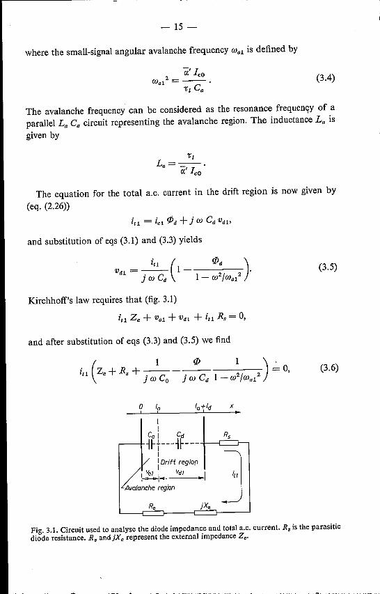
Kirchhoff's law requires that (fig. 3.1)
and after substitution of eqs (3.3) and (3.5) we find
(3.6)
x
II
Ca I Cd-H-t---~~---
I: Drift region
I va,_ I vd' I~.. ..Avalanche region J
Fig. 3.1. Circuit used to analyse the diode impedance and total a.c. current. R, is the parasiticdiode resistance. Rc andjXe represent the external impedance Ze·

in which we use the abbreviations
16 -
and (3.7)
The small-signal impedance Zl of the diode follows from eq. (3.6) and can bewritten
1 (jj 1Zl=R +---------sce 1 2/ 2'j W 0 j W d - W Wal
(3.8)
where we note that R, + l/jwCo is the impedance of the diode exactly at thepoint of breakdown (lco -+ 0).So much for the theoretical determination of the small-signal impedance. We
measured the small-signal impedance of several diodes at a fixed frequency inthe X-band as a function of the bias current through the diode. The meas-urements were carried out using the accurate microwave impedance bridgespecially designed by Van Iperen and Tjassens 38). On this bridge the small-signal impedance of the diode in its encapsulation is measured. The equivalentcircuit of the diode in its encapsulation as used in the calculation of the diodeimpedance from the measuring data is given in fig. 3.2.The capacitance C
IIIof
Fig. 3.2. Equivalent circuit ofthe diode in its encapsulation used in the calculation ofthe diodeimpedance from the measured impedance data. Cm is the capacitance of the encapsulation, andLm is the inductance of the mounting wire.
the encapsulation, typically 0·16 pF, was found by measuring empty encap-sulations. The inductance LIII of the mounting wire, typically O·5 nH, was foundby comparing the capacitance ofthe diode measured at 10 GHz withits capaci-tance measured at a frequency of 1 MHz, where the influence of the mountingwire can be neglected. At 1MHz the capacitance was measured with a BoontonCapacitance Bridge, Model 75D. A full discussion of the procedure described

/
- 17-
above, including an extensive error treatment, is given in the above mentionedpaper by Van Iperen and Tjassens 38).An example of the measured diode impedance is given in fig. 3.3. Before
6050
90V
80
70
Rs ID 2-0-RI (.Il)
Fig. 3.3. Example ofthe measured small-signal impedance (diode no. 4 in table 3-II, sec. 3.1.3).The angle tp to be used in eq. (3.9) is indicated.
-]0
-0-2 0+02
breakdown (circles) the bias voltage is the parameter; after breakdown (dots)the bias current is the parameter, The measuring frequency is 10 GHz. Thefigure shows that for the current range indicated a linear relation between theimaginary and real parts of the diode impedance is found. Indicated in fig. 3.3is the angle cp to be used in the "tan ip" method for the determination of diodeparameters. This method will now be discussed.
3.1.2. Diode-quantity analysis; tan cp methodIn what follows we assume that we know the small-signal impedance data of
the diode measured at a single microwave frequency äs a function of the biascurrent through the diode. The values of the various diode parameters (diodequantities) used in the preceding section can be found from these measured databy assuming that they can be described by eq.(3.8),i.e. by our theoretical expres-sion for the small-signal diode impedance.If Z, = R; + jXl and Xo = l/jwCo, it follows from eqs (2.25), (3.7) and
(3.8) that tan cp, as indicated in fig. 3.3, is givenby
Xl - Xo Re (/J la/Id + (sin 8)/8tan cp = = - -- = ------
R, - R, Im (/J (1 - cos 8)/8(3.9)
By way of example, tan cp is plotted in fig. 3.4 as a function of 8 for severalvalues of la/Id' •
From eq. (3.9) it is concluded that tan cp is a function of geometrical diodequantities and the frequency, but not of the bias current. The theory thus

(3.10)
- 18-
Fig. 3.4. The function tan rp, eq. (3.9), as a function ofthe transit angle IJ for several values ofthe ratio 1./ Id'
predicts the linear relationship between Xl and RI as already mentioned at theend of sec. 3.1.1. For all diodes investigated experimentally this linear relation-ship was found for Ico smaller than 10 to 15mA. Deviations are found at highervalues of the bias current. These deviations are due to the effectof the bias cur-rent on the width W of the depletion layer via Poisson's equation and viatemperature effects (note that in our diode model W was assumed to be aconstant; assumption (5) in sec. 2.4)From the experimentally determined value of tan cp (eq. (3.9))and the trivial
relation
where Ow = (.()W]o, the ratio I./Id and 0 can be found 35) if Wand v are known.The width of the depletion layer was always calculated from the breakdownvoltage and the manufacturing data of the diode, assuming a constant impuritydistribution in the epitaxial layer. It was also assumed that the depletion layerwas never restricted by the substrate on which the epitaxial layer was grown. Inthe case of the diodes investigated experimentally this assumption was verifiedby means of C-V measurements. In the calculations (see sec. 3.1.5)the saturateddrift velocity v, also needed to calculated Ow, was taken from table 3-1, i.e.from the literature. We shall come back to this particular choice of Wand vat the end of this section.
TABLE 3-1
Table of constants used in the calculations
semi- m oe P Vn vpcon- (m/s) (m/s)ductor a (m-I) b (V/m) a (m-I) b (V/m)
Si 1 2'40.108 1'60.108 1,80.109 3,20.108 1,05.105 0,96.105pe 1 1,55.109 1'56.108 1.00.109 1,28.108 0·6 .105 0·6 .105GaAs 2 3,50.107 6,85.107 3·50. 107 6·85. 107 0·9 .105 0·6 .105
(3.11)
-19 -
Since we now know the values of W, la, Id and 8, the transit-time function (]Jis also known. Using the experimental value of Xo, the values of Ca and Cdcanbe calculated. The quantity 'ä'/7:ICm which together with the bias current deter-mines the avalanche frequency Wal (eq. (3.4)), can be found from the graphRl(lco) or from the graph X1(lco), using the following relations:
or
((lXl ) ( a' ) Re (]J
(llco IcO=O = - 7:1 Ca W3 Cd'(3.12)
These relations are found after differentiation of the real and imaginary partsof eq. (3.8) with respect to the bias current.Using the tan cp method, we thus determined all the diode quantities needed
to calculate the diode impedance. It should be noted that this method does notprovide for a value of 'ä' or 7:1' Only the ratio of these two quantities is knownat this point of our investigation. In chapter 4 it will be shown that 7:1 can bedetermined from microwave noise measurements on the non-oscillating diode;'ä' can then be calculated from 'ä'/7:I'In the foregoing the value of W was calculated and that of v was taken from
the literature. This might strike the reader as strange since the available imped-ance data can be arranged so that it is possible to determine 8 and la/Id (andhence (]J, Ca and Cd) from these data without making assumptions for Wand v.It follows from eqs (3.4) and (3.8) that
(3.13)
where X = -w Cd/lm (]J. From eqs (3.9) and (3.13) it then follows that
sin 8 (1 - cos 8)1--
8- + (tan cp + XXo) 8 = 0, (3.14)
and 8 can be found from this relation if tan cp, Xo and X are known. The quanti-ties tan cp and Xo are determined as described before. The quantity X followsfrom the graph (R; - Rs)-l as a function of lco-1; X can only be determinedaccurately when X and the other terms in eq. (3.13) are of the same order ofmagnitude. This condition is satisfied for rather high values of lco. However,we then find that the diode model adopted is inadequate to describe the imped-ance data correctly. At these high bias currents the imaginary part of Z, is nolonger proportional to the real part of Zl' Moreover, eq. (3.14) cannot solve

-20 -
all our problems since to find the length of the drift region it is in any casenecessary to make assumptions, either about v (Id from e) or about the actualjunction area (Id from Cd)' Because of all these arguments we decided to cal-culate the value of Wand to take the value of v from the literature.
3.1.3. Experimental results
With a view to studying the intrinsic response time in particular (chapter 4),we measured and analysed the small-signal impedance data of several diodestructures: Si p+-n, Si n+-p, n-Si Schottky-barrier, Ge n" -p and n-GaAsSchottky-barrier diodes. The results relevant to the measurements and analysisare summarised in table 3-II. All diodes are of the mesa type. In diodes 1-8 and
TABLE 3-I1
Diode quantities as determined from the measured impedance data; VBR is thebreakdown voltage of the diode
diode material/ VBR W Xo tan cp e uw ä'j-CI Cano. type (V) (um) (n) (rad) (A-1 S-1)
1 Sip+-n 65 3·0 46 2·8 1·14 0·38 46. 10212 Sip+-n 66 3·1 36 2·7 1·16 0·37 31 . 10213 Sip+-n 68 3·2 48 3·3 1·05 0·43 48 . 10214 Sip+-n 100 5·3 47 1·9 1·83 0·42 22.10215 Si nr=-p 70 3·3 22 1·1 1·82 0·18 23. 10216 Si nr=p 110 5·8 34 0·8 2·68 0·28 16 . 10217 Si n+-p 111 5·8 43 1·0 2·55 0·33 18 . 10218 Si nr--p 111 5·8 41 1·0 2·55 0·33 19 . 10219 n-Si S.B. 70 3·5 70 1·9 1·44 0·31 51 . 102110 Gen+-p 32 2·6 30 1·6 1·82 0·34 36. 102111 Gen+-p 33 2·8 29 1·3 1·99 0·31 23 . 102112 Ge nr=p 33 2·8 25 1·4 1·93 0·33 21 . 102113 n-GaAs S.B. 55 2·5 20 2·2 1·33 0·33 16 . 102114 n-GaAs S.B. 50 2·2 31 2·0 1·22 0·23 25. 1021
diodes 10-12 the junction was formed by diffusion (diffusion depth about1·5 fl-m) into an epitaxiallayer on a good-conducting substrate. Diodes 1 and 2were fabricated from the same slice of epitaxial material, as were diodes 7 and8, and diodes 11 and 12. Diodes 9, 13 and 14 were of the Schottky-barriertype 39). The metal used for diode 9 was palladium, while titanium was usedfor diodes 13 and 14.
- 21-
The measuring frequency was 10 GHz for all diodes. The impedance datawere obtained as described in sec. 3.1.1 and the data were analysed using thetan cp method. From the eighth column of table 3-II we find thàt the ratiola/W is ~ 0'4, 0'3, 0·3 and 0·3 for the Si p+-n, Si n+-p, Ge n" -p and n-GaAsSchottky-barrier diodes, respectively. Except for the Si n+-p diodes these ratiosagree fairly well with computer calculations of the diodes (see sec. 3.1.5). It canbe shown that better agreement between theory and experiment can be obtainedby taking the effect of diffusion of the free carriers in the depletion layer andthe actual doping profile, and hence the actual field profile, into account 40).
Diffusion effects require a diode model whose large-signal and oscillator-noisebehaviour in particular can hardly be traced analytically. However, for thediodes investigated on oscillator noise (chapter 6), it was found that neglectingthe effects of carrier diffusion in the theory had no serious consequences. Wetherefore ignored these effects in our theoretical studies.
3.1.4. Extension of the diode modelTo obtain some insight into the relevance of the data. derived in the preceding
section, we extend the diode model.In sec. 3.1.2 we concluded that for the diode model used (sec. 2.4) the circuit
representation of the avalanche region is a simple La Ca parallel circuit. Frommore-detailed studies it has been concluded that this circuit has to be extendedwhen the model of the avalanche region is refined. We recall some of the majorresults of these studies without discussion:(a) A resistance in series with the inductance La has to be added to account for
the differential static resistance of the avalanche region and for transit-timeeffects on the conduction current in that region 41.42). This differ-ential resistance is, generally, negative and independent of the frequencyco. The effect of the transit time is generally also negative and is propor-tional to co2 42).
(b) A parallel resistance has to be added to the circuit to account for the carrier-induced displacement current 33,36), which results from the fact that"öJiox =1= O.The parallel resistance can be transformed into a resistance inseries with La. This resistance is then proportional to co2• The effect of thisdisplacement current may be positive or negative 33).
(c) Ifthe saturation currentis taken into account, the d.c. current multiplicationfactor Mo = leo/Is is no longer infinitely high. A finite Mo can be represent-ed by a series resistance of La. The value of this resistance is equal toI/Mo "(X' Ieo 41).
We now assume that all effects found from more-detailed studies of theavalanche-region properties may be represented by a resistance Ra in serieswith the inductance La 35) (fig. 3.5):
Ra = R + Sco2,

- 22-
Fig. 3.5. Extended small-signal circuit representation of the avalanche region.
where Rand S are independent of frequency. With this extended description ofthe avalanche region the expression for the diode impedance remains valid,provided we replace the avalanche frequency Wal by the complex avalanchefrequency Wal defined by
- 2 2/ ')Wal = Wal (1 -Ja, (3.15)
where a = r]» + SW,
r = R/La,s = S/La.
The equivalent expression for tan tp, eq. (2.9),is now given by
Re (jj - h Im (jjtan cp = - ,
Im (jj + h Re (jj(3.16)
where(3.17)
From the foregoing discussion we expect a to depend on the bias current. Onthe other hand it was found experimentally (fig. 3.3) that (XI-Xo)/(RI-Rs)is a constant when the impedance is measured at a microwave frequency and atvalues of the bias current which are not excessively high. It can therefore beconcluded that under these (experimental) conditions the terms containing hin eq. (3.16) can be neglected, since we know from the results given in table 3-IIthat tan cp is larger than zero. So h cannot be determined from the experimentaldata discussed. In principle it is possible to determine h from the small-signalimpedance data of the diode measured as a function of frequency for a givenvalue of the bias current. The value of the frequency should be varied fromvalues well below Wal up to values well above Wal> while wal/2n is of the orderof magnitude of 3 GHz. These data, however, are difficult to obtain with suf-ficient accuracy. We therefore performed numerical calculations to obtainvalues of ZI(W), and used these values as "measuring data" in the analysis ofthe diode quantities in our extended analytical diode model.
In the computer calculations the drift velocity of the electrons and holes isassumed to be completely saturated throughout the depletion layer. The field

-23 -
dependence of the ionisation coefficient of the electrons, 0:, and that of the holes,{J, is described by
0:, {J = a exp [- (b/E)m].
The constants a, b and m, and the velocities Vn and vp used in these calculationsare listed in table 3-1. The static breakdown characteristics and the small-signal impedance were calculated numerically *). The latter calculations areanalogous to those described by GummeI and Scharfetter 43). Thus the con-tinuity equations and current equations are solved directly without making theassumption that the depletion layer can be separated into an avalanche regionand a drift region.
Calculations were made first for two silicon diodes: an n+ -p and a p+ -ndiode, both having the same form of the impurity distribution N(x):
N(x) = =F 4,7.1015 ± 1.2.1021erfc(1·96.104 x) cm=". (3.18)
The current density Jco was taken as 106A/m2 (= 10mA/1002 (Lm2)in accord-ance with a practical situation. Results relevant to the static behaviour of thediodes are summarised in table 3-III, where Vo is the bias voltage and Ro the
TABLE 3-III'"Numerically calculated quantities relevant to the static behaviour of the two
diodes of eq. (3.18). Current density 106 A/m2; junction area 10-8 m2
1035·5048
Vo (V)W({Lm)s, (n)
1095·66102
static differential resistance (space-charge resistance) of the diode. The nu-merically calculated admittance as a function of frequency is represented bythe dots in fig. 3.6. The continuous curves in this figure are calculated from theextended analytical diode model (in which a separation into an avalanche regionand a drift region is assumed), after least-squares adjustment of the parametersr, s,fal = Wal/2n, and Id, using the dots in fig. 3.6 as "measuring points". Thelength W needed for this adjustment was taken from table 3-III. The results forthe adjusted parameters are given in the left-hand section of table 3-IV. Asshown in fig. 3.6, the analytical expression, viz. eq. (3.8) with the avalanchefrequency Wal replaced by the complex avalanche frequency Wal given by eq.
*) The computer program was made by J. de Groot and H. Knoop of our laboratory.

-24 -
Re V,(.Il-I)
t 3.10-3
JmV,(.Il-I)
t10.70-3
- f(GHz}10
a} b}
Fig. 3.6. Small-signal admittance as a function of frequency for the two diodes of eq. (3.18).The marks (triangles: p+ -n, dots: n+ -p) refer to numerical calculations. The drawn curveswere calculated from eq. (3.8), with Wal = Wal given by eq. (3.15), after least-squares adjust-ment to the numerically calculated points. Junction area 10-8mê ; d.c. current 10-2 A;R, = O.(a) Real part admittance; (b) imaginary part admittance.
TABLE 3-IV
Diode quantities relevant to the diode impedance as determined from thenumerically calculated impedance data of the two diodes of eq. (3.18). Currentdensity 106 A/m2; junction area 10-8 m"; (a) by the least-squares method; (b)by the tan cp approximation
(a) (b)least-squares tan cp approx.
nr=p »r-« nr=p p+-n
r (S-l) -0.4.109 -0,2.109 - -S (s) -0,8.10-12 -2.1.10-12 - -a (GHz) 3·3 3·0 - -a (GHz) from eq. (3.11) - - 3·5 3·2
fa (GHz) from eq. (3.12) - - 3·4 3·1Id (urn) 4·6 3·4 4·5 3·6Id/W 0·82 0·61 0·79 0·65(J (rad), Cf= 10 GHz) 3·03 2·01 2·95 2·15

N(x) = 7.5.1015 - 1.2.1020 erfc (2.104 x) cm=", (3.19)
- 25-
(3.15), gives an excellent description of the numerically calculated points overa large range of frequencies. The assumption that all extensions of the modelfor the avalanche region can be combined into the series resistanceR; = R + S w2 therefore also seems to be correct.
Secondly, calculations were made of the small-signal impedance for the sametwo diodes at a fixed frequency (10 GHz) as a function of the bias current. Theresults of these calculations are presented in fig. 3.7. From this figure it can be
-90,-----,------,-----,------,-----,----,
X,(.a)
t10
-1 -2-R,(.f1)
Fig. 3.7. Numerically calculated small-signal impedance as a function of the bias current forthe two diodes of eq. (3.18). Junction area 10-8 rnê ; frequency 10 GHz; R, = o. The angle tp,eq. (3.16), is indicated.
observed that a linear relationship exists between the real and imaginary partsof the impedance, as was found for the experimental data (sec. 3.1.1). Thus theinfluence of h on tan cp, eq. (3.16), is once again negligible. From eq. (3.17) itfollows that h « 1 if a «1 and if, at the same moment, Wa1
2jw2 « 1. Usingthe figures given in the left-hand section of table 3-IV it is found that h = 0·06and 0·14 for the n+ -p and p+ -n diode, respectively. It is therefore reasonable tostate that for values of the bias current which are not too high, and for X-bandfrequencies, we may reduce eq. (3.16) to eq. (3.9) used in the tan cp method.When the latter method was used for the analysis of the computer data given infig. 3.7, the figures in the right-hand section of table 3-IV were found. Thesefigures show good agreement with the results obtained by the least-squaresmethod using the extended analytical diode model. As mentioned before, thetan cpmethod gives us no information about rand s, and therefore none about h.
Thirdly, calculations *) were made for a silicon n+ -p diode as a function offrequency and the bias current, in order to obtain some insight in the currentdependence of r, s, !al' Wand Id. The impurity distribution of this diode isgiven by
*) In these calculations vp(Si) was taken as 0.75.105 mIs, instead of 0.96.105 ms, whichwas used in all other calculations.

- 26-
The results of the analysis of these data, using the least-squares adjustment tothe extended, analytical expression of Zl(a», for several values of leo, are givenin fig. 3.8. We conclude thatla/ is indeed proportional to leo (see eq. (3.4)) andfurthermore that the length of the depletion layer and that of the drift regionincrease slightly with increasing bias current, as is to be expected. The quantitys does not depend very markedly on leo, whereas the dependence of r on leo ismore pronounced as will be shown in sec. 3.1.5.From fig. 3.8 it can be concludedthat, at least for this diode, a = ria> + s a> increases with increasing biascurrent.
(,2 ~/d 5 ra(GHz2) {Jlm) (ps) (5-1)
t 50 5t fa] t -2.0.109 tW
""..
Id "30 3'" '" -1.2.109
»:"..
,,/r -0-8'" ----
Ia - ~--s-.--0·4 -0.4.109'_It'
:.-'0 V 00
0 la 20 30 40 500
+-r-s,» (mA)
Fig. 3.8. Diode quantities for the diode of eq. (3.19) as a function of the bias current. Thequantities were found after least-squares adjustment of eq. (3.8), with Wal = Wal given byeq. (3.15), to the numerically calculated small-signal impedance over a frequency range 0-12GHz.
The ratio ~/17:1 can be determined from the data given in tables 3-111and3-IV. For the known value of la the average electric field in the avalanche regioncan be found using the breakdown condition (eq. (2.5)). The value of~' can thenbe calculated from eq. (2.22),so that 7:1 is known. Using the figures given in theleft-hand section of table 3-1Vwe thus find for the two diodes of eq. (3.18):
Si n+-p, la = 1·0 (J.m: 7:1 = 4·3 ps,
Sip+-n, la = 2·1 (J.m: 7:1 = 6·5 ps.
The intrinsic response time 7:1 will be discussed further in chapter 4. The abovedata are also presented in fig. 4.5.
3.1.5. Discussion
(1) The first assumption listed in the summary of assumptions in sec. ~.4 wasthat the depletion layer can be divided into an avalanche region and a driftregion. From fig. 3.6 it can be concluded that the analytical model in which thisdivision was made, accurately describes the numerical data, in the calculation

-27-
of which the division was not made. The first assumption in sec. 2.4 thereforeseems to be appropriate, at least for the small-signal case.(2) The second assumption made in sec. 2.4, resulting in the simple Read
equation (2.27),placed fairly tight restrictions on the model of the avalancheregion. However, comparing the data in the left-hand section of table 3-IV tothose in its right-hand section, we draw the cónclusion that if Wal < wand thevalue of the bias current is not too high, this second assumption is also appro-priate. This conclusion is supported by the experimental data shown in fig. 3.3,which indicate that a current range exists in which Xl depends linearlyon R,as is demanded by the simple analytical model.(3) The third assumption in sec. 2.4 states that we consider the diode to have
only one drift region. Figure 3.9 gives the carrier-generation function for the
2.106
IdJ~~col(m-I)
EoMm)
4./07 1
a)0:2 0·4 0·6 OB
_xlW
J.l07~f--- n+-p p+-nEO(Vlm)
t2./07
/07: : :
I I I
o ' :, :,o 0·2 0·4 0·6 0·8 to
_xiVv'b)
Fig. 3.9. (a) Electric-field distribution and carrier-generation function for the two diodes of eq.(3.18), as found from numerical calculations. The ratio Id/ W, as found from the least-squaresadjustment (table 3-IV) is indicated for both diodes. (b) Equivalent field distribution.
two diodes of eq. (3.18), resulting from the numerical calculations of thestatic-behaviour characteristics. This generation function is defined as theabsolute value ofthe space derivative ofthe normalised electron current densityIJn/Jcol· The junction field strength is also shown and, drawn on this scale, isabout the same for the two diodes. The relative length of the drift region asfound by the least-squares method is also indicated. For the n+ -p diode it isthen found by integration of the generation function that 96% of the carriergeneration takes place outside the drift region, while the corresponding figure

-28 -
for the p+ -n diode is found to be 90%. The generation function of the latterdiode suggests, however, that a second drift region has to be taken into accounton its left-hand side. Assuming somewhat arbitrarily that the generation func-tion has the same value at the two boundaries of the avalanche region (as indi-cated by the dashed line in fig. 3.9), a relative thickness of 0·05 of the left-handdrift region is found. Then 89% of the generation takes place outside the twodrift regions.
In the case of two drift regions eq. (3.9) has to be modified and becomes
(3.20)
where the subscript I stands for the larger of the two drift regions and thesubscript 2 for the other ..When deriving eq. (3.20) it was assumed that
Id2 I-cos B2 I-cos BI----«----Idl
and
Thus, if eq. (3.9) is used, it follows from eq. (3.20) that if Id2 « Idl the transitangle of the largest drift region is found, while the length of the avalancheregion might be too large by an unknown amount Id2•
With the assumptions made so far, together with the results obtained in sec.3.1.4, the field profile given in fig. 3.9a can be reduced to those for the n+-p andr:-n diodes as shown in fig. 3.9b.
When the least-squares adjustment method, discussed in the preceding section,was extended to include a second drift region, again a relative thickness ofR:j 0·05 for this region was found in case of the p+ -n diode. The other diodequantities obviously change slightly in this process. However, none of theconclusions concerning h or a is modified. In the remainder of our studies thepossible effect of a second drift region is therefore neglected.
The saturation current Is was neglected in all derivations and numericalexamples. If Is is taken into account Mo = leo/Is < 00, while Mo contributesto a by an amount I/wMo7:i• At relevant values of the bias current Mo isabout 107• The intrinsic response time is about 5 ps, so that at microwave fre-quencies, say w = 2n. 1010 S-l, the contribution to a is about 3.10-7 and hencenegligible. At low frequencies and low bias currents a significant contribution ofMo to a is possible. That, however, is irrelevant to the present study.
Low-frequency measurements are found to be not very suitable for the

- 29-
determination of diode quantities. This can be illustrated as follows. From eqs(3.8) and (3.15) it can be calculated that
12 I'lim Zl = R, + __d_ + == Ro.<0-+0 28 V A Wal
2 Co
The second term on the right-hand side of this equation is the well-knownexpression for the space-charge resistance of the drift region. The third termarises from the space-charge resistance of the avalanche region. It is found fromexperiments and from numerical calculations that, as a first-order approxi-mation, Ro is a constant at not too high values of the bias current. Hence I'
varies as a first-order approximation in the same way with lco as Wal2 does(see also fig. 3.7). The influence of I'/WaI
2Co therefore cannot be eliminated bymeasuring Ro at various values of lco. From the data given in tables 3-II1 and3-IV it is found that for the two diodes of eq. (3.18) I'/WaI
2Co is 5% and 6% ofRo for the n"-p and p+-n diode, respectively. In an analysis 35) similar to thatperformed in sec. 3.1.4 the present author has found values of 2% and 27 % ofRo to be possible for I'/WaI
2Co. Furthermore, the measured value of Ro can beinfluenced by temperature effects (sec. 3.2.5). We therefore conclude thatrelatively large errors may be made when Id is determined from Ro withouttaking the space-charge resistance of the avalanche region into account.
3.2. Large-signal theory
When studying the noise properties of the oscillating diode it is important toknow the behaviour of quasi-stationary quantities such as the large-signal imped-ance of the diode, and the signal level of the oscillations. Furthermore, it isvery important to know the range of signal levels for which the large-signaltheory used is valid.
The large-signal impedance is calculated in sec. 3.2.1. This is followed by adiscussion of the oscillation condition in sec. 3.2.2. From this discussion weshall learn that, if the external circuit is fixed, both the oscillation frequency andthe avalanche frequency in the model used are constants. In sec. 3.2.3 the rangeof validity of the noise-free large-signal model used is determined from simpleoutput-power versus bias-current measurements.
Section 3.2.4 discusses the microwave impedance measurements. From themeasuring data it is possible to determine the large-signal impedance of thediode, the circuit loss resistance, and the effective load resistance of the oscil-lator.
Finally, in sec. 3.2.5, the theory is extended to include the effect ofthe second-order field derivative of the ionisation coefficient, ~". By including ~" it shouldbe possible to explain the rectification effects of the r.f. signal, the so-called"d.c. restorage" . The experiments, however, are found not to confirm this; ~"
(3.21)

- 30-
is therefore left out of the theoretical description, except when in sec. 5.4.3 the"down-conversion" of oscillator noise is discussed.
3.2.1. Large-signal impedance
The large-signal impedance is calculated starting from the assumptions con-cerning the diode model summarised in sec. 2.4. We furthermore assume thediode to be placed in a singly tuned, low-Q circuit which at a fixed frequencymay be described as shown in fig. 3.10. In this circuit we disregard the build-upof harmonic voltages and in our calculations we consider the fundamental
Fig. 3.10 Block diagram of the oscillating loop and definition of the impedances, see text.
harmonic of the a.c. current only. The bias current is assumed to be suppliedfrom a constant current source.The large-signal diode impedance is Z = R +jx. Its real part R is considered
to consist of the resistance of the active part of the diode Rdepl> and of a lossresistance R, (see fig. 3.10). The circuit is represented by a loss resistance R;andaload impedance ZL = RL + jXL. Seen from the diode the extemal irnped-ance is Ze = R; + ZL' The r.f. current in the loop is it, the r.f. voltage acrossthe diode V"~
Let the voltage across the avalanche region be Va = VaD + Va sin tat, Vao
being the d.c. part and Va sin cot the a.c. part, with Va a real number. Integra-tion of the Read equation (2.27) then yields
t,= loo exp ( ei' Va (1 - cos wt)),to 't' I
(3.22)
where loo is an integration constant. From this equation it follows that thefundamental harmonic ie of le is given by 42.44)
;:y=-.
«rr I(3.23)

-31-
In the derivation of eq. (3.23) from eq. (3.22) use was made of the Pourierseries 45)
00
exp (- x cos wt) = ~ (- I)Y ly(x) exp (j v w t),v=-oo
where lv(x) is the modified Bessel function of the first kind, with order v andargument x. The time-independent factor in eq. (3.22) was removed by therequirement that the conduction current averaged over one period of w beequal to the bias current leo, the latter being supplied from a constant currentsource. Equation (3.23) indicates that ie lags 90° behind Va. In fig. 3.12 in sec.3.2.3 the ratio 11(yva)/10(Yva) is represented by the drawn curve.As in the small-signal case, Va also excites a displacement current, given by
j w Ca Va. Addition of this current to the conduction current gives the total a.c.current it:
it = ie + j w Ca Va = j W Ca Va ( 1- ::) = ie ( 1- :a:). (3.24)
where the avalanche frequency Wa is defined by
W/ 2 11(YVa)--=-----,Wa/ Y Va 10(Yva)
(3.25)
Wa12 being defined by eq. (3.4).To find the total impedance of the diode we can proceed as in the small-
signal case (sec. 3.1.1), since all further operations are linear operations. Thesame expression is found for this impedance as in the small-signal case, providedwe replace the small-signal avalanche frequency in eq. (3.8) by the large-signalavalanche frequency defined by eq. (3.25). Hence Z is given by
1 cp 1Z=Rs+----- .
j W Co j W Cd 1 - w2/w/(3.26)
It should be noted that in this expression Wa is the only parameter that dependson the bias current and the signallevel. We make use of this in a discussion ofthe oscillation condition below.
3.2.2. Oscillation condition 46)
Por stable oscillation the oscillator loop must satisfy the condition that thetotal loop impedance vanishes at the oscillation frequency (wo). Using theimpedance definitions given in fig. 3.10, this condition implies that
Rs+ Rdcp1 + jX+ Ze = 0, (3.27)
- 32-
where Rdep1 + R, = Re Z and X = Im Z. After substitution of eq. (3.26), thiscondition can be written
(3.28)
For a given diode, i.e. for a given fixed set of geometrical diode quantities{la, Id, A}, and a given fixed external circuit, the right-hand side of eq. (3.28)is a function of Wo only. This function is indicated by g(wo). Because the av-alanche frequency Wo defined in eq. (3.25) is a real quantity, the oscillationcondition eq. (3.28) can now be expressed by the identities
(3.29a)
(3.29b)Img(wo) = O.
We observe that the oscillation frequency Wo is fully determined by eq. (3.29b)and is influenced neither by the a.c. voltage nor by the bias current, sinceg(wo)does not depend (in our model) on Ieo and Va' Consequently, it follows fromeq. (3.29a) that the avalanche frequency is a constant, too, and thus Wo = wa•s!'
where wa•s! is the small-signal avalanche frequency at the start of the oscil-lations (note that we assumed the external circuit to be fixed). Using eq. (3.4),eq. (3.25) can be written
W2a (3.30)--=--=-=--
Wa12
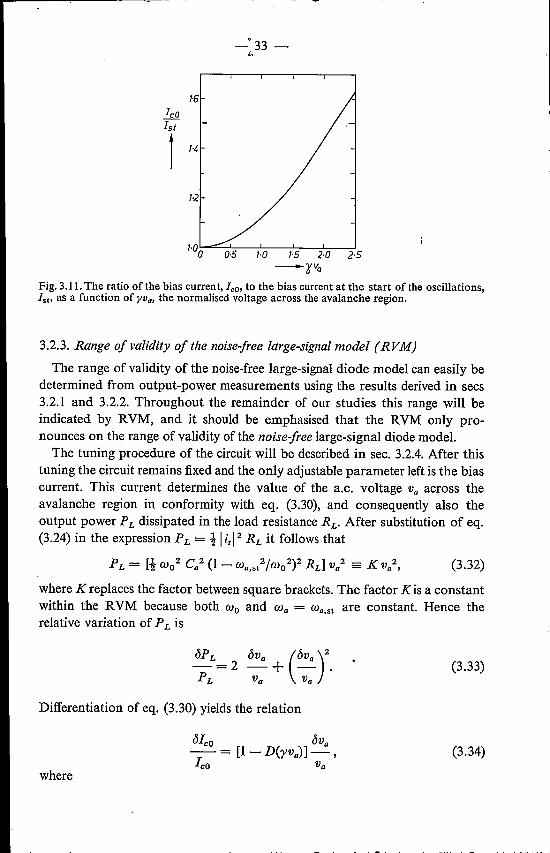
where Is! is the bias current at the start ofthe oscillations. We observe from thisequation that if the bias current Ieo is varied the a.c. voltage Va must vary insuch a way that the avalanche frequency Wo remains a constant equal to wa•s!·
The value of Is! follows, for example, from the real part of eq. (3.27):
(3.31)
In the actual circuit Is! can be measured, and eq. (3.30) can be used to determinethat value of Y Va for a given value of Ieo (fig. 3.11).It should be emphasised that the above discussion is only valid if the shift of
the oscillation frequency caused by varying leo, as is found in practice, has anegligible effect on the circuit impedance. For a discussion ofthe current depend-ence of Wo see the next section.
1·6
-·33.c..
1·2
1·5 2·0 2·5-'Kva
Fig. 3.11. The ratio of the bias curren t, leo, to the bias current at the start of the oscillations,ISh as a function of YVa, the normalised voltage across the avalanche region.
3.2.3. Range of validity of the noise-free large-signalmodel (RVM)
The range of validity of the noise-free large-signal diode model can easily bedetermined from output-power measurements using the results derived in secs3.2.1 and 3.2.2. Throughout the remainder of our studies this range will beindicated by RVM, and it should be emphasised that the RVM only pro-nounces on the range of validity of the noise-free large-signal diode model.
The tuning procedure of the circuit will be described in sec. 3.2.4. After thistuning the circuit remains fixed and the only adjustable parameter left is the biascurrent. This current determines the value of the a.c. voltage Va across theavalanche region in conformity with eq. (3.30), and consequently also theoutput power PL dissipated in the load resistance RL' After substitution of eq.(3.24) in the expression PL = ti itl2 RL it follows that
(3.32)
where K replaces the factor between square brackets. The factor K is a constantwithin the RVM because both Wo and co; = Wa•st are constant. Hence therelative variation of PL is
(3.33)
Differentiation of eq. (3.30) yields the relation
(3.34)
where

-34-
(3.35)
We note that eq. (3.35) represents the ratio of the slopes of the tangent to thechord ofthe function ll(yva)/lo(Yva) which is represented by the drawn curve infig. 3.12. The dashed curve in this figure represents the function [l-D(yva)]-l.
{t-O(yva)F' (' ) tan exI,(Y va)
Dy Va= tan fJ Io(YVa)
+ 10 1·0
tI11
5 0·5
-__2 4 60
-rva
Fig. 3.12. The function I1(yv.)/Io(Yva) (drawn curve) from which D(yv.) can be determined,and the function [l-D(yv.)]-l (dashed curve), which relates the output-power variations tothe bias-current variations.
If we apply an artificial variation in lco, small enough for the second term onthe right-hand side of eq. (3.33) to be negligible, we find
2(3.36)
and hence the function D(yva) can be determined from the P L(IcO) charac-teristics as YVa follows from eq. (3.30),i.e. from the ratio lst/lco. Figure 3.13agives an example of the measured D(yva) compared with the theoretical D(yva)for an Si n+-p diode and an n-GaAs Schottky-barrier diode (see also chapter 5,table 5-1). In these two examples the diodes have an RVM up to YVa R:i 1·8andYVa R:i 2·2, respectively. It should be noted that to determine the RVM it issufficient to know the PL(lco) characteristic only. Neither the diode impedancenor the circuit impedance need therefore be known.In sec. 3.2.4 it will be shown that it is possible to establish the value of the
effective load resistance RL and the value of the total a.c. voltage Vr across thediode. If we define the modulation depth m by
(3.37)

- 35
1·0.-=----------.
D(yvaJ
t0·8
0·6
I-Or---.------,I
y(V-IJ /
t0'8---<... Diode nO.I4.0·6
III/
0.4.,_~----.,,/
""Diode no.7
- Theory• Diode no.7x Diodeno. 14
0·4
0·2 0-2
00 2 4. 6 8 10- Va (VJ
b)
2 3 4 5-_ YVa
aJFig. 3.13. (a) Experimental values of D(yv.) derived from the PL(Ico) characteristics for aSi 11+ _p diode (dots) and an II-GaAs Schottky-barrier diode (crosses). Oscillation frequency9 GHz. The drawn curve represents the theoretical values of D(yv.). (b) y as a function of Vafor the same diodes, and under the same experimental conditions as under (a). The valuesy(O) derived from the quantities given in table 3-I1 are indicated. The range in which y is aconstant determines the RVM.
where VBR
is the breakdown voltage ofthe diode, we find an RVM up to mm ax I":::!
0.12andmm•x ~0.22 for the siliconand the gallium-arsenidediode offig. 3.13,respectively, while the optimum modulation depth for these diodes is mopt(Si)~ 0.37 and mopt(GaAs) ~ 0·50. The optimum modulation depth, as definedby Van Iperen and Tjassens 38,47), is the modulation depth corresponding tothe maximum output power for a given value of the bias current when theload resistance is varied. The optimum modulation depth is found to be nearlyindependent of the bias current. As shown by Van Iperen and Tjassens 38,47),
and as also follows from our large-signal impedance measurements, themaximum attainable modulation depth is slightly higher. Thus we find that ourlarge-signal diode model describes about 40 % of the possible range of modula-tion depths.It might be felt that the model is useful in only a small range. However,
neither an analytical nor a numerical diode model has yet been reported inthe literature that describes the diode impedance over a substantially largerrange of modulation depths. Moreover, as will be clear later on in our studies,the RVM covered by our model is still of interest in the study of noise inIMPATT -diode oscillators.
Since, as mentioned, RL can be found from large-signal impedance meas-urements, the constant Kin eq. (3.32)can be determined, as all diode quantitiesare known from the analysis of the small-signal impedance measurements.Va can therefore be calculated sinceP L can be read from a power meter. Thus ycan be determined as a function of Va. The results for y(va) for the diodes offig. 3.13a are given in fig. 3.13b. In fig. 3.13b the RVM is given by the range inwhich Y is a constant (indicated by the drawn curves), since our diode modeldemands for a constant y (the RVM which can be read from fig. 3.12a is of

-36-
course the same as the RVM which can be read from :fig.3.13b). Also indicatedin :fig.3.13b is y(O), calculated from the small-signal data given in table 3-II.Taking into account the rather large number of independent measurementsneeded to arrive at :fig.3.13b, it is concluded that the internal consistency of thedata is good (for the diodes summarised in table 5-1it was found that the twovalues of y at Va = 0 matched within 16%).We next consider the shift of the oscillation frequency which is found in
practice when the bias current is varied (as mentioned before, the oscillatorcircuit is :fixed).When the bias current is varied, we observe a variation of thebias voltage. The latter means that the width of the depletion layer also variesand hence the cold capacitance Co of the diode. If we assume (a) that for thediodes studied 1/Co2 oe Vo, (b) that XL = col: where L is a constant, and (c)that the variation of the oscillation frequency is predominantly caused by thevariation of Co, it can be easily demonstrated that the fourth power of theoscillation frequency is proportional to the diode bias voltage. As shown in:fig.3.14, this relationship is satis:fiedvery well within the RVM of the diodes .
7.2.703
f"(GHz")
t 6.8.103
• Diode no. 7x Diode no. 14
54 56 58 60 62 Diode ro.t;-Va (V)
Fig. 3.14. Fourth power of the oscillation frequency as a function of the bias voltage acrossthe oscillating diode for an Si n" -p diode (dots) and an /I-GaAs S.B. diode (crosses). TheRVM is indicated for both diodes.
Furthermore, we conclude that within the RVM the total frequency shift issmaller than 1%. This was found to be so for all diodes investigated. We there-fore neglected this frequency shift as far as it concerns the diode impedance andthe output power for which the RVM is applicable. This frequency shift wasalso neglected when the intrinsic oscillator noise, chapter 6, was studied.The diode loss resistance R, was always taken from the small-signal imped-
ance data at the point of breakdown, as indicated in :fig.3.3. It should, how-ever, be emphasised that at very high r.f. signallevels and at high input levelsR, can depend to an appreciable extent on the signallevel 48) and on the tem-perature. Within the RVM of the diode the r.f. signal and the input level arerelatively low. We therefore assumed R, to be constant.

- 37-
3.2.4. Microwave impedance measurements
The large-signal diode impedance, Z, and the circuit quantities such as thecircuit loss resistance R; and the load resistance RL were measured by a methodoutlined by Van Iperen and Tjassens 38.47). We shall briefly recapitulate thesteps in the measuring procedure.(a) The small-signal impedance ofthe diode at a fixed frequency, say 9 GHz, is
measured as a function of the bias current up to a value of Rl which issomewhat higher (to account for Rc) than the highest value of RL to beused. In this way the small-signal impedance will be known at all values ofthe start oscillation current that are of interest to us.
Fig. 3.15. Schematic diagram of the coaxial oscillator circuit.
(b) The diode is mounted in a coaxial oscillator circuit as sketched in fig. 3.15.The circuit is tuned in such a way that the oscillations start at the frequencyat which the small-signal impedance was measured (9 GHz in our example).If one slug is used, the tuning procedure is trivial. If two slugs are used, thetuning procedure is as follows. Slug 1, which is closest to the diode, is tunedso that the oscillations start at 9 GHz. At a bias current slightly higher thanthe start oscillation current slug 2 is tuned for maximum output power. Thelatter tuning causes a small shift ofthe oscillation frequency. In an iterativeprocedure slugs 1 and 2 are then readjusted so that the desired start oscil-lation frequency and maximum output power "coincide". We never usedmore than two slugs. It is felt that in this way the oscillator is always singlytuned correctly.
(c) After tuning the circuit remains fixed. Then the output power dissipated inthe load resistance is measured. Since the diode impedance is known at thestart ofthe oscillations, {Rl> Xl}' we also know the total circuit impedance,which is the complementary impedance {-Rl' -Xd. Various values ofthecircuit impedance were obtained by inserting slugs of various inside diam-eters. We thus obtained (fig. 3.16) a plot of the output power as a functionof Rl = RL + Rc, with the bias current as a parameter. The point P L = 0to which all the curves converge gives us the value of R; Hence we alsoknow RL'

- 38-
Diode no.8
PL(mW)
t
Fig. 3.16. Output power dissipated in the load resistance.Pj; as a function of Rc + RL = IRIl,as measured on an Si n+-p diode. The vertical lines indicate the values of Rc + RL for whichthe oscillator noise of this diode will be studied (diode no. 8 in table 5-1, sec. 5.4.1).
From the results given in fig. 3.16 it is possible to calculate the amplitude ofthe r.f. current it from the relationship PL = t Iitl2 RL, and the amplitude ofthe r.f. voltage Vt across the diode from
(3.38)
Figure 3.17 shows Rdep[ and X as a function of it with Ico as parameter for ann-GaAs S.B. diode (diode no. 14 in table 5-1). From these curves the diodeimpedance as a function of the bias current with the r.f. current as parametercan easily be derived. The results presented in fig. 3.17 will be used in chapter 5.
8-Rdepl(.a)
t
~ . 43~O 50 60 Ico=70mA X
x~~ 41(.[1,)
30 ~~ 39t~~~ 372
~~~--2=OO=-_L--4~0~0--L_~6~OO~O~--~-2-0LO--~-4-0LO--L_-6~OO~35
0)- Ît (mA) b) it (mA)
Fig. 3.17. Large-signal impedance of the active layer of an n-GaAs S.B. diode as a function ofthe total r.f. current it. The bias current lco is parameter (diode no. 14 in table 5-1, sec. 5.4.1).(a) Real part of the impedance (Rdep1 = R-Rs); (b) imaginary part of the impedance.
3.2.5. D.c. restorage
When measuring at equal values of the bias current the d.c. voltage acrossthe oscillating diode is found to differ from that across the non-oscillatingdiode, the temperature of the heat sink of the diode being kept constant. This

- 39-
difference is partly caused by temperature effects (ClVth), due to differences inpower dissipation. The other part is thought to be caused by rectification effectsof the r.f. signal (ClVor), the so-called d.c. restorage. If ClVo is the difference inbias voltage between the oscillating and the non-oscillating state, than
(3.39)
where(3.40)
In the latter expression Rth is the thermal resistance of the diode, dVo/dT de-scribes the change of the bias voltage with temperature, and Pout is the micro-wave power which leaves the oscillating diode and thus does not contribute tothe heating of the diode. ClVor can therefore be found from eq. (3.39) once ClVoand ClVth are known.The thermal resistance needed in eq. (3.40) can be measured as follows 42,49).
At a constant bias current the absolute value of the small-signal impedance ofthe diode 1z11 is measured as a function of frequency (fig. 3.18).The simplest
100
I.
~
r-==: - --IZ,(O)I~~
.
<, CrRr r-.=;
~-- - ---- -----
Ra
Iz,l(.fl.)
t 200
104 105 105
-f (Hz)
Fig. 3.18. Example of the low-frequency impedance as a function of frequency (diode no. 6 intable 3-H). The insert shows the simplest circuit with which the impedance data canapproximated. RT and CT are the temperature resistance and capacitance of the diode,respectively.
o
circuit with which the impedance data can be approximated is shown in theinsert in fig. 3.18. In ref. 42 it has been shown that Rth can be calculated from
s.; = RT[VO (dVo) J-1oC/w,
dT reO
(3.41)
where RT = 1Z1(0) 1 - Ro (see fig. 3.18). The quantity (dVo/dT)reo can bemeasured with the diode placed in an oven. Results for Rth for several diodes,

-40-
measured at leo = 10 mA, are given in chapter 5, table 5-1. It should be notedthat Rth is temperature-dependent, so that it depends on the bias current SO).
The precise form ofthe curve in fig. 3.18 contains information concerning thequality of the thermal contacts 42.47). We also note that eq. (3.21), which de-scribes the low-frequency diode resistance, is valid in this case for f > 1MHz,i.e. for j » 1/2nRTCT•
A theoretical estimate of c5Vor can be found only when the second- and higher-order field derivatives of the ionisation coefficient are taken into account.Limiting the Taylor expansion of (X to the second-order term, we find afterintegration of the Read equation:
{I [( (XII) (X'Ic = loo exp - (X la - 1+ - Va2 t + - (1 - cos rot) Va +7:1 4la CO
(X" J}- -- Va2 sin 2rot ;8 co la
(3.42)
see also eq. (3.22).
For periodic oscillations the coefficient of tin eq. (3.42) must vanish, so that
-If0(a la - 1+- v/ = o.41a
(3.43)
If c5Vao is the change of the d.c. voltage Vao across the avalanche region causedby the d.c. restorage, it is easily found from eq. (3.43) that c5Vao is well approx-imated by 42)
1 a"c5Vo = --- V 2 (3.44)a 41a(X' a,
where c5Vao = la c5Eao.A change c5Vao also influences the d.c. voltage VdO across the drift region.
An estimate for this voltage change is
and hence an estimate for c5VOr is given by
-11
0( 2-=; Va .0(
(3.45)

- 41-
Combining eqs (3.32) and (3.45), we see that öVor is proportional to the outputpower ofthe oscillator. Furthermore, since ä" and ä' are positive numbers öVoris negative. Figure 3.19 gives the measured d.c. restorage for diodes 14 and 7 of
Diode nO.4
0·6~V(V)
t0'4
0·2
c'iV
t -0·2
-0'4
Diode nO.7
200 300-PL(mW)
Fig. 3.19. Change of the bias voltage of the oscillating diode with respect to that of the non-oscillating diode as a function of the output power dissipated in the load resistance. The totalchange ijVowas measured for equal values of the bias current, and at a fixed temperature.ijVor is ijVo corrected for temperature effectsûiVOr= ijVO-ijVth). The RVM is indicated.(a) /I-GaAs Schottky-barrier diode (diode no. 14). The calculated d.c. restorage is indicated;(b) Si n+ -p diode (diode no. 7).
b) o
table 5-1 in sec. 5.4.1 as a function of PL' The dots represent the öVo and thecircles öVor according to eqs (3.39) and (3.40), where Pout was taken to be theoutput power dissipated in (R; + RL)' The latter choice is somewhat arbitrarysince a part of the output power dissipated in a part of R, might also be takeninto account. In the case ofthe GaAs diode (diode no. 14), where the ionisationcoefficients of electrons and holes are equal, ö Vor can be calculated accordingto eq. (3.45). The calculated ö Vor for this diode is also given in fig. 3.19a. Fromthis figure we conclude that there is no agreement between theory and experi-ment for this diode. The measured öVor in fact becomes positive within theRVM of the diode. For the silicon diode, where the ionisation coefficients areunequal, we have no expression available to calculate ä". Hence, for this diodewe have plotted öVo, and the measured öVor only. It is seen from this figurethat öVor is negative for all values of PL investigated. However, the experimentalcurve for öVor contains a part where the slope of the tangent is positive, whichis contrary to the theory.
_._-_ ..._------~--~-~---'--------"'---~----"~------

- 42-
The deviations mentioned were found to be the rule rather than the exception.We therefore conclude that our diode model is inadequate to describe thissecond-order effect. The quantitative description of the d.c. restorage, inparticular the positive d.e. restorage which has also been observed by others 31),is still unexplained. D.c. restorage, has, however, been mentioned in this sectionbecause it plays a part in the down-conversion ofr.f. noise in bias-current noise.

-43 -
4. NOISE OF THE NON-OSCILLATING DIODE
The output power of an oscillating loop can be considered to consist of nar-row-band amplified noise, as will be discussed in chapter 6. This noise isgenerated predominantly within the avalanche region of the diode. In thepresent chapter the noise of the non-oscillating diode is discussed, because atthe start of the oscillations the oscillator signal builds up itself from this noise.Furthermore, the intrinsic response time TI which governs the internal noiseproperties of the diode, can be determined from noise measurements on thenon-oscillating diode.Many studies have been devoted to the subject of noise in non-oscillating
diodes 6). We first give a brief historical review. The first theory to describe thecurrent fluctuations in the avalanche process was presented by Tager 51). Heassumed that the fluctuations of the conduction current flowing out of theavalanche region are due to the shot noise of the thermally generated currentand to the fluctuations in the number of electron-hole pairs created byeachprimary electron-hole pair. The diode model used by Tager was Read's diodemodel where, among other assumptions, Vn = vp and IX = p. Tager's theorywas further developed by McIntyre 52), who derived a more general expressionfor the noise generated in the avalanche region. His theory allows for Vn =l=vp,IX =1= P and an arbitrary electric-field profile. Both authors considered thefluctuation of the conduction current in the avalanche region only, i.e. theyconsidered the primary noise current to be discussed in sec. 4.2. However, thetotal noise current flowing through the diode is also influenced by displacementcurrents and the transit-time effect of the carriers in the drift region. Theseeffects were first studied theoretically by Hines 8), who used an analysis basedon the small-signal-impedance theory given by Gilden and Hines 53). Thetotal noise current caused by the noise source to be introduced in sec. 4.1, willbe calculated in sec. 4.2.The studies on noise in avalanche photodiodes have also contributed to the
understanding of the noise behaviour of the avalanche process. Of these studieswe mention the theoretical work of Emmons and Lukovsky 28) and the exper-imental work of Melchior and Lynch 54). These four workers were especiallyinterested in the frequency dependence of the noise current at low values of thebias current, such that the carrier multiplication factor has to be considered asfinite.
Of more recent date is the theoretical work of Cla assen 32), Kuväs andLee33) and Convertê"), From these studies we can obtain explicit expressionsfor the intrinsic response time which governs the internal noise properties ofthe diode, i.e. the primary noise current. All investigations mentioned abovedeal with the noise problem analytically. A numerical investigation has beenmade by Gummel and Blue 55).

- 44-
In the literature there is very little quantitative information, based on exper-iments, available on the intrinsic response time. We therefore carried out noiseand impedance measurements at microwave frequencies in order to determine7:1 experimentally. The measurements will be described in sec. 4.4. Low-fre-quency noise measurements will be discussed in sec. 4.5.
In sec. 4.3 the influence of the extension of the diode model, as described insec. 3.1.4, on the noise properties of the non-oscillating diode will be discussed.In that section, too, the possibility of noise sources other than the one intro-duced in sec. 4.1 will be explored.
4.1. Introduction of the noise source
The total noise current flowing through the diode is predominantly causedby the noise of the random impact-ionisation process. Therefore in the presentsection only the conduction current in the avalanche region is considered.
For the description of the noise behaviour of a device one seeks for the placein the description of the device where it is justifiable to introduce a white noisesource. After introducing this source the total noise current through the devicecaused by this source is determined. In our opinion it is correct to introduce thewhite noise source in the continuity equations for the electrons and holes, eqs(2.8) and (2.9). For the sum of the continuity equations we then obtain
(4.1)
while the difference of the two equations remains unaltered:
(4.2)
The noise generation is represented by gn in eq. (4.1). The latter equation hasthe form of a Langevin equation 27). For simplicity of presentation we onceagain, as in the derivation ofthe Read equation, eq. (2.18), limit the calculationsto the case fJ = IX, Vn = Vp = v, where IX and v are assumed to be independentof the position. The final equations will be refined afterwards.The white noise source represented by gn is assumed to be a shot-noise
source of the following. From the condition of a steady, high-current avalanchewhere the number of thermally generated electron-hole pairs can be neglected,we know that the average number of electron-hole pairs created by an initialpair during its transit through the avalanche region is unity. The length la of theavalanche region is of the order of 1 (Lm.The energy of a carrier needed to makean ionising collision possible is about 3/2 times the band-gap energy of thesemiconductor 24). Hence, for silicon the carrier must have an energy 81 of

-45 -
about 1·5 eV. A carrier has gained this energy from the electric field E whenit has travelled a distance It = etfqE. A typical value of E in silicon is 3'5.107V/m. Thus for silicon It ~ 0·04 (.Lm, and hence It «: la (the same argumentsapply to germanium and gallium arsenide). We therefore think it justifiable tostate that the ionisation probability of a carrier depends on its instantaneousenergy only and not on the previous carrier history. As a result, if we consideran infinitesimal volume at a fixed position within the avalanche region, weknow that a large number of ionisations take place in this volume but that theprobability that a carrier will ionise precisely in this volume is completelyrandom. Hence the mean-square value of the fluctuations of the conductioncurrent dIe generated within this volume is given by the shot-noise relation
«dIe - (dle»)2) = 2 q <dIe) dj,
where dj is the bandwidth considered.The next step to be made is to calculate the influence of the shot noise
generated in the :fixedinfinitesimal volume, on the total conduction currentleaving the avalanche region. In addition we must integrate over the shot-noisecontributions of all infinitesimal volumes which together form the avalancheregion. From the foregoing it will be clear that we can assume that all volumesgive the same initial shot-noise contribution.
4.2. The total noise current
For the calculation of the total noise current through the diode we assumethe diode to be placed in a circuit similar to that of fig. 3.1. Proceeding uponthe lines along which the Read equation, eq. (2.18), has been derived, it iseasily found from eqs (4.1) and (4.2) that
7:a d--Ic = Ic(IX la-I) + gn(x),3 dt .
where we neglected the saturation current, and where gn(x) is the initial shot-noise source at the position x in the avalanche region, as described in sec. 4.1.The conduction current le consists of a d.c. component lCD and a noise com-ponent ine• After linearisation of eq. (4.3) we obtain the relation
In like manner as in the calculation ofthe small-signal impedance, see eqs (3.1)to (3.8); we find for the total noise current dint flowing through the diodecaused by gn(x):
(4.3)
(4.4)
(4.5)

-46 -
Since we are dealing with noise, the mean-square value of dint is of interest,hence
2 q <dlc> dJI f[J 1 1 12
«dint)2> = W2 (-r:a/3)2 W Cd 1 - Wa//W2 21 + Ze
(4.6)
In this equation g/(x) is replaced by the shot-noise relation, where <dIe> is theaverage current generated in the infinitesimal volume at x in the avalancheregion. The total noise current caused by all initial shot-noise sources in theavalanche region is found after integration to be
'a<int2> = J «dint)2> .
o(4.7)
So we have to calculate the integral
'a 'aJ <dIc> = J <et (In + lp» dx = eto Ico la = i.;o o
After generalisation to et =1= (J, Vn =1= Vp, as in eqs (2.19) to (2.22), we find:
2 q leo dj 1 f[J 1 1 12
<i 2> _nr - 2 2 -_ 2/ 2 - ,
«r v, W Cd 1- Wal W Z,(4.8)
where Z, = 21 + Ze. Equation (4.8) is equivalent to eq. (19) of Hines's originalnoise theory 8). Although Hines introduced his noise source in a completelydifferent way we both find the same expression for the total noise current. Itmight be the subject of a separate study to investigate whether the two deriva-tions of the total noise current should indeed give the same answer or that theequivalence of eq. (4.8) and eq. (19) of ref. 8 is quite fortuitous.
Equation (4.8) can formally be written
where F is a transfer function. The noise current ino is generally called theprimary noise current. This current is the noise current which would flow in theavalanche if it were possible to maintain the electric field constant (in time)at the exact critical value needed to maintain a steady avalanche 8). Since
2 q I dl"<. 2> _ eO '.IlnO - ,
w2-r:/(4.9)
- -47-
it should be noted that "' is the only diode parameter that determines theprimary noise current.We finally mention that eq. (4.8) is based on the assumptions on the diode
model summarised in sec. 2.4, and that this equation can also be found startingfrom eq. (4.4) where gn(x) has been replaced by (2 q lco df)1/2, i.e. from 11)
(4.10)
Then, of course, the integration eq. (4.7)must be skipped. Furthermore, thevalues of t-: and Vno are r.m.s. values in this case.
4.3. Extension of the diode model; discussion
In secs 4.1 and 4.2 itwas assumed that the dominant noise source is the noisegenerated in the avalanche process. Further possible noise sources are:(1) The thermal noise from the passive diode resistance and circuit resistance.The noise contributions of these resistors follow from the well-known Nyquisttheorem: vn2 = 4 kT R dj It was found that in all experimental situations thisnoise contribution could be neglected.(2) The thermal noise generated in the drift region of the diode. This noisecontribution can be estimated from the "impedance-field method" developedby Shockley et al. 56), which gives the noise voltage induced at the terminals ofa device by the thermal velocity fluctuations of carriers at an arbitrary placewithin that device. For the mean-square open-circuit noise voltage per unit. bandwidth the impedance-field method yields the following expression in thecase of a one-dimensional structure of length (W - la) and area A 56):
< 2) IV I()Z ( ) 2VnO d = 4 q2 A J n(x) D(x) ~l dx.
dj öx(4.11)
In this expression n is the time-average density of the free carriers, D thediffusion constant of the carriers, and ()Zn/()x the impedance-field vector withrespect to the terminal. For the drift region, in which the carriers travel atsaturated drift velocity v, it is then found 57) that
(4.12)
where use has been made of lco = n q V A, since n is indepeneent of x.The diffusion constant D was assumed to be independent of x, since we areinterested here in an estimate of the noise source only. In fig. 4.1 eq. (4.12) ispresented graphically for diode no. 6 of table 4-1 (sec. 4.4), assuminglco = 10 mA and D = 80 cm2fs. This value of D is the average high-field dif-

-48 -
Fig. 4.1. Calculated open-circuit noise voltage per unit bandwidth (for diode no. 6 of table 4-1)as a function of frequency, at a bias current of 10 mA, caused by the noise generated in theavalanche region and in the drift region.
fusion constant (E = 400 kVlcm) for electrons and holes in an avalanche insilicon 5S-60). It is felt that this value leads to a reasonable upper limit of thenoise contribution of the drift region. Also presented in fig. 4.1 is the open-circuit noise voltage per unit bandwidth which follows from eq. (4.8):
2 I 1""12q eo 'P' 1(4.13)------=----- ----- -----------
dj
The value of the intrinsic response time needed in the calculation was obtainedfrom eqs (2.5) and (2.20), using the constants given in table 3-1.We concludethat for this diode the noise generated in the avalanche is indeed the dominantnoise contribution. Within the range of frequencies of interest this was foundto be the case for all diodes investigated, as will be discussed further at the endof sec. 4.4. Below, therefore, we shall consider the noise generated in theavalanche only.In sec. 3.1.4 the diode model was extended with respect to that summarised
in sec. 2.4. In the extended model we accounted for the differential staticresistance of the avalanche region, for transit-time effects in that region, etc.

-49 -
Itwas found in sec. 3.1.4 that all effectswhich were found from a more detailedstudy of the avalanche region could be summed up in the parameter a, whichgives rise to a complex avalanche frequency Wal defined by eq. (3.15):
-2 2/(')Wal = Wal 1-Ja.
When this extension of the diode model is applied to the description of thenoise behaviour of the diode we find for the total noise current:
(4.14)
The difference between eqs (4.8) and (4.14) is that 7:, has been replaced by7:, (1 - ja). This leads to the complex avalanche frequency Wal of eq. (3.15) andto 7:12 (1+ (2) in the denominator of the primary noise current (see eq. (4.9)).Equation (4.14) can be rewritten as
(4.15)
where h = a/(l-wa//ro2), as in eq. (3.17). In sec. 3.1.4 it was concluded thatat not too high values of the bias current and at microwave frequencies, so thatroal2/ro2 «: 1, the value of awas small compared to unity, and hence h «: 1.Wethen can conclude from eq. (4.15) that under the same conditions int is correctlydescribed by the simple-model equation (4.8). At low frequencies a significantcontribution of a is possible, but the condition h «: 1 can be satisfied at valuesof the bias current such that Wa12 » Ial ro2. In practice this means that fco
should be larger than, say, 10 (LA.In the remainder of our studies we areinterested in the noise behaviour of the diode at a frequency of 200 kHz and atX-band frequencies, say 9-10 GHz, while the bias current is always largeenough. Therefore, we shall use eq. (4.8), which is based on the assumptionssummarised in sec. 2.4.Finally, in this section we mention that at values of the bias current and at
values of the frequency such that roa/ «: ro2, eq. (4.8) predicts that the noisepower is proportional to the bias current, and inversely proportional to ro4 ifthe frequency dependence of cp is neglected. These predictions have beenverified by experimental studies carried out by Constant et al. 61) and by Haitzand Voltmer 62). An example ofthe bias-current dependence ofthe noise powerat 10 GHz for two of our diodes investigated is given in fig. 4.4 in sec. 4.4.
4.4. R.f. noise measurements-
The r.f. noise current was measured to obtain, in combination with theimpedance measurements discussed in sec. 3.1, an experimental value of theintrinsic response time 35.63). For the noise measurements the diode (in itsencapsulation) was placed in a mount connected to an X-band radiometer. The
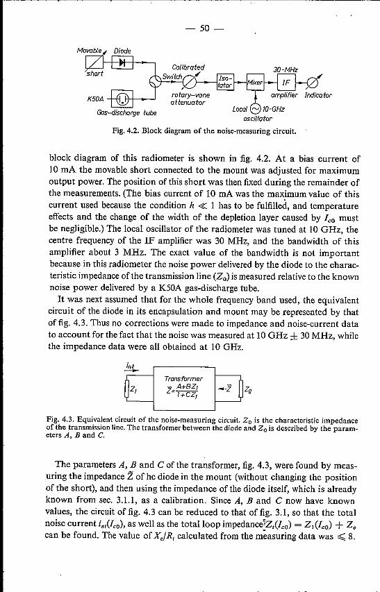
- 50-
Diode
oscillator
Fig. 4.2. Block diagram of the noise-measuring circuit.
block diagram of this radiometer is shown in fig. 4.2. At a bias current of10 mA the movable short connected to the mount was adjusted for maximumoutput power. The position of this short was then fixed during the remainder ofthe measurements. (The bias current of 10 mA was the max!mum value of thiscurrent used because the condition h « 1 has to be fulfilled, and temperatureeffects and the change of the width of the depletion layer caused by lco mustbe negligible.) The local oscillator of the radiometer was tuned at 10 GHz, thecentre frequency of the IF amplifier was 30 MHz, and the bandwidth of thisamplifier about 3 MHz. The exact value of the bandwidth is not importantbecause in this radiometer the noise power delivered by the diode to the charac-teristic impedance ofthe transmission line (Zo) ismeasured relative to the knownnoise power delivered by a K50A gas-discharge tube.It was next assumed that for the whole frequency band used, the equivalent
circuit of the diode in its encapsulation and mount may be represented by thatof fig. 4.3. Thus no corrections were made to impedance and noise-current datato account for the fact that the noise was measured at 10 GHz ± 30MHz, whilethe impedance data were all obtained at 10 GHz.
TransformerZ=A+BZ,
I+CZ,Za
Fig. 4.3. Equivalent circuit of the noise-measuring circuit. Zo is the characteristic impedanceof the transmission line. The transformer between the diode and Zo is described by the param-eters A, Band C.
The parameters A, Band C of the transformer, fig. 4.3, were found by meas-uring the impedance Z of he diode in the mount (without changing the positionof the short), and then using the impedance of the diode itself, which is alreadyknown from sec. 3.1.1, as a calibration. Since A, Band C now have knownvalues, the circuit of fig. 4.3 can be reduced to that of fig. 3.1, so that the totalnoise current int(lco), as well as the totalloop impedance~Zt(lco)= ZI(lco) + Z,can be found. The value of Xc/R, calculated from the measuring data was ~ 8.

- 51-
10./0-18
30./0-18
/Zt!2. i;t=sr:(V2.S)I 20.10-
18
4 6 8 10-Ico{mA)
Fig. 4.4. Example ofthe quantity in,z IZtl2/dfas a function of the bias current as found fromthe experiments. The diode nos. 4 and 6 refer to the diodes in table 4-1.
o 0 I 2
This justifies the assumption that we may use the circuit of fig. 4.3 with fre-quency-independent values of the parameters over the frequency range10 GHz ± 30MHz.Figure 4.4 gives an example ofthe parameter in/ IZtl2fdfas a function ofthe
bias current. The intrinsic response time was determined from the slope of thetangent through the origion of the graph:
(4.16)
using the data obtained from the impedance measurements summarised intable 3-11.The data relevant to the measurements and analysis described are summarised
in table 4-1.The results for r, as a function ofthe length ofthe avalanche region(see also table 3-11) are presented graphically in fig. 4.5, together with thetheoretical curves of r, obtained from eq. (2.20). Also plotted in this figure arethe values of .1 for the two diodes of eq. (3.18), sec. 3.1.4, and the point{.I = 3 ps, la = 0·3 [Lm} reported by Melchior and Lynch for a germaniumavalanche photodiode 54). From fig. 4.5 we conclude that eq. (2.20) correctlypredicts the dependence of r, on la in the range investigated. However, we alsoconclude that there is a systematic discrepancy between the numerical exper-imental and theoretical values. This discrepancy, which has also been' observedby Naqvi 64) and by Kuväs and Lee 65), can be removed by taking the effect ofcarrier diffusion into account 60.65.66). The effect of carrier diffusion is to

- 52-
TABLE 4-1Diode quantities as determined from the measured noise current and imped-ance data for the same diodes as given in table 3-II, and the ratio(vno2)d/(Vno2)a, see text
Fig. 4.5. The intrinsic response time as a function of the length of the avalanche region, asfound from the experiments. Black triangles: Si P+-/l, dots: Si /I+-P, black square: /I-SiSchottky barrier, black triangles upside down: Ge /1+ -P, crosses: /I-GaAs Schottky barrier, andas estimated for the two diodes of eq. (3.18), open triangles: Si p+ -/I, circles: Si /1+ -p; opentriangles upside down: Melchior and Lynch 54). The drawn curves where calculated from eq.S2.20) using the constants of table 3-I.
Ti(ps)
t
diode material/ VBR la 7:1 '(X' (vno2)d/(Vno2)ano. type (V) (urn) (ps) (V-I) co
1 Sip+-n 65 1·2 3·6 0·15 0·12 Sip+-n 66 1·2 3·6 0·14 0·13 Sip+-n 68 1·4 3·8 0·14 0·14 Sip+-n 100 2·2 6'1 0·11 0·35 Si n+-p 70 0·6 2·7 0·25 0·26 Si nr=p 110 1·6 4·0 0·10 0·57 Si n+-p 111 1·9 5·0 0'10 0·68 Sin+-p 111 1·9 4·6 0·10 0·69 n-SiS.B. 70 1·1 3·6 0·13 0·1
10 Gen+-p 32 0·9 6·8 0·35 2·011 Ge n+-p 33 0·9 7·7 0·30 3·212 Gen+-p 33 0·9 7·5 0·31 2·913 n-GaAsS.B. 55 0·8 7·7 0·28 4·614 n-GaAsS.B. 50 0·6 6·4 0·29 3·7
0-4060-81 2 4-la (pm)

- 53-
increase the intrinsic response time since, owing to back-stream diffusion ofcarriers, the after-effect of a deviation from the steady state lasts longer. If theeffect of carrier diffusion is taken into account, then the influence of this dif-fusion on the passage of the carriers through the drift region must also be takeninto account. This, of course, influences the value of 'tI determined from theexperiments, as has been shown by Hulin et al. 60). However, diffusion effectsare not considered in the theoretical part of our studies, in order, particularly,to keep the large-signal theory analytically traceable. On the other hand, whenin the remainder of our studies we compare theory and experiment, the value of"I found experimentally, as given in table 4-1,will be used.Finally, we shall look at the noise contribution of the drift region, as discus-
sed in sec. 4.3. From eqs (4.12) and (4.13) we obtain the relation
(4.17)
At microwave frequencies and for not too high values of the bias current, suchthat wa//w2 « 1, the last term between brackets is almost unity, thus makingthe ratio given by eq. (4.17) independent of lco' The ratio (in %) is given in thelast column of table 4-1 for the diodes investigated, using the data given intables 3-1, 3-II and 4-1, and the average high-field diffusion constantsD(Si) = 80cm2/s for E = 4ookV/cm 58-60), D(Ge) = 100cm2/s for E =200 kV/cm 60), and D(GaAs) = 250 cm2/s for E = 400 kV/cm 60). Since wetook D constant in the drift region and the values of D used are maximumvalues, we may conclude from the last column that only a small error in 'tI ismade when the noise contribution of the drift region is neglected.
4.5. L.f. noise measurements
In chapters 5 and 7 it will be discussed that low-frequency noise, so fluctua-tions of the bias current, under certain conditions in the bias circuit of theoscillator can give a contribution to the oscillator noise. Therefore, it is ofrelevance to consider the low-frequency noise of the non-oscillating diode first.The expression for the total noise current through the diode, eq. (4.8),
contains the totalloop impedance Zl + Ze. We assume the frequency to beso low that only the real part of Ze has to be considered, and that Re Ze = RB,where RB is the bias resistance. In sec. 3.1.5 (eq. (3.21)) and in sec. 3.2.5 (fig. 3.18)we have seen that the simple diode model used can give rise to relatively largeerrors in the calculation of Ro, the low-frequency limit of Zb and also thattemperature effects can influence the actual value of Ro' Therefore, we considerthe total noise current to be generated by a noise voltage source <Vn0
2)1/2 in

- 54-
series with the diode. From eq. (4.8) it follows for (J) -->- 0 that
(4.18)
where use has been made of
W2
lim Iq>12 = - ."'-+0 II
Equation (4.18) predicts that <vn02) is inversely proportional to the bias currentlco. This prediction has been verified in a comprehensive study of the homo-geneity of the avalanche breakdown of a junction by Haitz 67). A plot of thenoise voltage per unit bandwidth for diode no. 7 of table 4-1 is presented infig. 4.6. This experimental curve was traced from the continuously recorded
w(V)
t
~00----.-,----T::":"-7"--:::--1Diode nO.7f =200kHzdf=IOOHz
~L.I~--~-u~~~~ILO~~~~,OO-Ico(mA)
Fig. 4.6. Open-circuit noise voltage as a function ofthe bias current for diode no. 7 oftable 4-1.Curve a was calculated from eq. (4.18) using (2 la = 1·90. 10-7 m/Y (see table 4-1); for curve bex' la = 1·48 . 10-7 m/Y is used, which follows if carrier diffusion is taken into account 40).Curve c is the experimental curve.
curve on an x-y recorder. For a comparison with theory we must know thevalue of a'. This value can be obtained from the factor a'/'tICa given in table3-11, since Ca and 'tI are now known quantities, while the factor a'/Olea was notused in the calculation of 'tI from the experimental data, as can be concludedfrom eq. (4.16). The results ofthe calculation ofa' are given in the sixth columnof table 4-1, and presented graphically as a function of la in fig. 4.7. Also givenin this figure are the theoretical curves calculated from eq. (2.22), and it isconcluded that the experimental data are in close agreement with the theory.In fig. 4.6, two theoretical curves are drawn relating <vno2) to leo- The lower
curve was calculated from eq. (4.18) and from the relevant quantities given intables 3-11 and 4-1 obtained from the microwave measurements. For diodeno. 7 the quantity a' la is equal to 1'9.10-7 m/V. Ifthe microwavemeasurementsare analysed, as is done in ref. 60, i.e. carrier diffusion is taken into account, and

- 55-
0·100·08
0·06··
02 0·4 0,6 OB 1-0 2·0 4·0-la (pm)
Fig. 4.7. The field derivative of the average ionisation coefficient as a function of the length ofthe avalanche region, as found from the experiments (black triangles: Si p+ -n, dots: Si 11+-p,black square: /I-Si Schottky barrier, black triangles upside down: Ge 11+-p, crosses: n-GaAsSchottky barrier). The drawn curves were calculated from eq. (2.22) using the constants oftable 3-1.
the actual doping profile is also taken into account, it is found for diode no. 7w
that f~' dx = 1.48.10-7 m/V 40). Using 'ä' la = 1.48.10-7 V/m in eq. (4.18),o
the upper theoretical curve in fig. 4.7 is found. We conclude that in the inter-mediate bias-current range there is good agreement between theory and exper-iment, particularly if we reckon with (1) the large number of independentmeasurements needed to arrive at the diode quantities, and (2) with the factthat all diode quantities were determined from measuring data at microwavefrequencies. At low values of the bias current we measure some excess noisedue to the fact that the avalanche in this diode is not completely uniform overthe junction area 66). At higher currents, too, excess noise is found, due tothermal effects: the current in the centre of the diode becomes lower than in theperiphery of the diode 67). Furthermore the temperature affects the value of 'äand as a result the value of 'ä'. Both 'ä and 'ä' decrease with increasing tem-perature 68). In addition, la and Ware influenced by the temperature of thejunction.
Finally, we mention that the pole at leo = 0 in eq. (4.18) is only an apparentone, the main reason being that eq. (4.18) is not valid at very low values of leo·At very low values ofthe bias current eq. (4.15) should be used.

-56-
5. OSCILLATOR NOISE
5.1. Introduction
The practical application of an IMPATT-diode oscillator depends to a largeextent on its noise characteristics, i.e. on the amplitude and frequency fluctua-tions of the output signalof the oscillator. In this chapter we first shall brieflydiscuss some of the ways one can describe the fluctuations, and give measurescommonly used to quantify the fluctuations (sec.5.1). This is followed in sec.5.2 by a description of the noise-measuring equipment. In sec. 5.3 a very briefsurvey will be given of the general, phenomenological theory of oscillator noisewhich, in principle, is applicable to any oscillator. This chapter ends with anapplication of the general oscillator-noise theory to the special case of ourIMPATT-diode oscillators.The simplest way to look at the "quality" of the output signal is to use a
spectrum analyser. This apparatus displays the output power PL dissipated inthe load resistance as a function of frequency. The output power is measuredin a narrow frequency band dj, averaged over a time interval which is longcompared to I/dj The resulting "picture" is called the spectrum, an exampleof which is given in fig. 5.1. The centre frequency fo of the spectrum is calledthe oscillation frequency or carrier frequency. A measure for the quality of thespectrum of the output signal is its width 2 LIlo which is the frequency intervalaround fo determined by PL(/O ± iJfo) = iP L(/O)' The spectrum width is in-dicated in fig. 5.1. For a spectrum of the form as given in this figure it applies
PL (f) (dB)PL (fa)
1-20
-30
-40
-60
-cr) L-J'-----'-:--::-±-.,-,-I----:---='::=7:-,L-_.L._j_fa-200kHz fa+200kHz200kHz fa=9GHz _ f
Fig. 5.1. Spectrum of the output signalof diode no. 7 in table 5-1, oscillation level such thatrVa = 0·6. Horizontal scale 200 kHz/division, vertical scale 10 dB/division. The spectrumwidth 2 LIlo around the oscillation or carrier frequency Jo is indicated, as are the upper andlower sidebands, of width 1 kHz, at a distance of 200 kHz from the carrier. The spectrum wasdisplayed with an HP852A spectrum analyser, dynamic range 60 dB.

- 57-
that the smaller the spectrum width the better the quality of the output signal,i.e. the lower the oscillator noise. The bandwidth dfused when measuring theoutput power should be small compared to the spectrum width, 2 Llfo·When using a spectrum analyser we face two problems. The first problem is
that it is impossible to conclude from the spectrum displayed whether it isbrought on by amplitude fluctuations (AM noise), by frequency fluctuations(FM noise) or by a mixture of both. The second problem is the rather smalldynamic range of the analyser (for example 60 dB), which limits the measurableratio PL(f)/PL(fO)' Therefore another measuring technique has to be applied.This technique, for which a more detailed description of the spectrum is needed,will be discussed in sec. 5.2. This description is based on the fact that most of theoutput power is contained in a rather narrow band around fo (fig. 5.1). There-fore, the output spectrum can be thought to consist of a carrier of frequency focontainingall the output power, and an upper (f> fo), and a lower (f <fo)noise continuum. It is useful to subdivide the noise continuum into a largenumber of strips of bandwidth df69). The noise power within each strip (side-band) may then be replaced by a sinusoidal voltage source of frequency f andvoltage Vn0 The frequency fis the mean frequency of the noise sideband consid-ered. The frequency J,m defined by J,,, = f - fo, gives the distance (in frequency)of the sideband from the carrier atfo' In our studies we shall only consider thenoise sidebands for which 2 Llfo «t; «t; Furthermore, we restrict thediscussion to those cases where the carrier power is very much larger than thenoise power in the sideband considered.We next consider the carrier and the noise sidebands at Q = 2 nfm from the
carrier. In fig. 5.2a the three corresponding voltage vectors are drawn in thecomplex plane. The carrier vector rotates at frequency Woanti-clockwise in thisplane. The amplitude of the carrier voltage is a constant. The noise vector ofthe upper sideband rotates anti-clockwise at frequency Q with respect to thecarrier, while that of the lower sideband rotates clockwise at Q with respect tothe carrier. The circle in fig. S.2a indicates schematically the r.m.s. value of Vno
which is assumed to be the same for the upper and lowerside bands (symmet-rical spectrum). Addition of the two noise vectors to the carrier vector givesthe instantaneous signal voltage VS.
The signal can also be considered as a carrier which is simultaneouslyamplitude-modulated and phase-modulated by the noise. If Vnr is the resultantof the two noise vectors, the amplitude modulation is determined by its com-ponent parallel to the carrier vector, and the phase modulation by its com-ponent perpendicular to the carrier vector. We illustrate this as follows. In fig.5.2b the upper-sideband noise vector is decomposed by replacing it by twoparallel vectors Vn * of length vn/2, both rotating anti-clockwise at frequency Q.A noise vector Vam * of length vn/2 rotating clockwise at frequency Q is addedsymmetrically with respect to the carrier. The vector Vam * is compensated at any

- 58-
a) -Re b) _Re -Re
Fig. 5.2. Vector diagram of the carrier voltage Vc, and the upper- and lower-sideband voltageVn at angular frequencies Wo, Wo + Q, and Wo - Q, respectively.(a) Considering the carrier and the noise sidebands at Q from the carrier only, the signalvoltage Vs = vc(wo) + vn(wo +Q) + v,,(wo - Q). The upper- and lower-sideband vectorsrotate at angular frequencies Qand -Q, respectively, with regard to the carrier.(b) Decomposition of the upper-sideband noise vector into AM (vam·, vn·) and FM (VCm.,v .. ) noise vectors. Iv"l = Ivnl/2; Iv,,"'1 = Ivam·1 = Ivcm"'l. The resultant of vam'" and u.,"is always parallel to Vc, the resultant of VCm'" and vn• is always perpendicular to Vc' A sim-ilar decomposition can be made for the lower-sideband noise vector.(c) On the average, the end point ofthe resultant VlIr of the upper- and lower-sideband noisevectors will be on an oval as indicated.
time by the vector vfm *. The resultant of the vectors Vn * and Vfm * is alwaysperpendicular to the carrier vector, and determines the phase fluctuations. Asimilar decomposition can be made for the lower-sideband noise vector. Thedecomposition is based on the relation for an amplitude-modulated signal,
Vn Vn= Vc cos Wol + - cos [(wo + Q) I + 'lji] + - cos [(wo - Q) I + 1jJ], (5.l)
2 2
and that for a phase-modulated signal (vn «vc),
V',f = Vc cos ( Wol + :: sin (QI + 1jJ)) =
Vn Vn= Vc cos Wol + - cos [(wo + Q) I + 'lji] - - cos [(wo - Q) I + 1jJ]. (5.2)2 2
From fig. 5.2a, band eqs (5.1) and (5.2) we conclude that for each sidebandthe AM noise power is equal to the FM noise power (white noise). However,it is found experimentally that, in general, the AM noise power is about 40 dBbelow the FM noise power, as will be discussed in detail in sec. 5.4.2. This canbe understood by recalling that the non-linearity of the oscillating diode limitsthe magnitude of the output signa1.Thus the diode has a kind of built-in auto-

- 59-
matic gain control 70) which limits the amplitude fluctuations of the signalvoltage. A comparable mechanism is not present for the phase fluctuations, sothat these are larger than the amplitude fluctuations. We conclude that theremust be a strong correlation between the upper- and the lower-sideband noisevector, in such a way that the resultant of these vectors predominantly givesrise to phase fluctuations. This is illustrated in fig.5.2e, where it is indicated that,on the average, the end point of the resultant of the noise vectors and that ofthe signal voltage are on an oval. The length of the short axis of the oval isdetermined by the amplitude fluctuations, while that of the long axis is deter-mined by the phase fluctuations.
The instantaneous signal voltage can be written as
Vs(t) = [vc + Vam COS (Qt + 'Ijl)] COS (wot + v~~ sin (Qt + CP)). (5.3)
where Vam and VCm/vc are the instantaneous magnitude of the amplitude andphase fluctuations, respectively, and where Vam, VCm, 'Ijl and cp are assumed to beslowly varying functions of time compared to û:», Since the instantaneoussignal frequency cv is equal to the time derivative of the second cosine term ineq. (5.3), i.e. equal to
VCmcv = Wo + - Q cos (Qt + cp),
Vc
we can also speak of frequency modulation instead of phase modulation.A measure for both the AM and FM oscillator noise is the ratio, expressed
in dB, ofthe noise power in one sideband (ofwidth dj, at/m from the carrier)to the carrier power.A frequently used measure for the FM noise is the root-mean-square fre-
quency deviation iJ/rms• This quantity tells us how much, in frequency, thesignal frequency periodically shifts at a frequency fm, as shown by eq. (5.4).The relation between iJ/rms and the noise-power to carrier-power ratio men-tioned above is given by 69)
Pc 2/m2
In the case of a symmetrical spectrum of the form 1/(1+ x2), i.e. the spectrumcan be described by a Lorentz curve, the spectrum width 2 iJ/o is related toiJ/rms by the expression 11)
1(iJ/rms)2 = - 2 iJ/o dj,
2n
(5.4)
(5.5)
(5.6)

- 60-
where it was assumed that fm »2 Llfo and that the spectrum width was causedby FM noise only.
5.2. Experimental arrangement
In this section we describe the equipment used to measure AM and FMoscillator noise, and bias-current noise. A diagram of the system, subdividedinto 7 parts, is given in fig. 5.3. The oscillator-noise receiver, given in part 7,is based on ideas set forth by Ondria 69), and Schiek and Köhler 71). The
Fig. 5.3. Diagram of the noise-measuring system (see text).
.- microwave load,
'""IV'- fixed attenuator,
AfZ) adjustable attenuator,
A0 calibrated rotary-vane attenuator,
!fJ0 phase shifter,
'i:::=. directional coupler,-- isolator,~
~
3-port circulator,
microwave switch,
@ thermistor power meter,
@ spectrum analyser.

- 61-
calibration bridge, given in part 6, has been described by Schreiber andHecker 72). We shall now first discuss the seven parts of the diagram individ-ually, after which the AM-noise-measuring procedure and the FM-noise-measuring procedure will be described.
Part 1. Oscillator under testThe coaxial oscillator used has already been described in sec. 3.2.4. The
oscillator signal is fed into a 3-dB power divider which is terminated on one portby a microwave load and on the other port by the circulator Cl in part 5. Theoscillator is biased via the inner conductor ofthe load and the power divider bymeans of the circuit of part 2. Used in this way, the power divider and loadprevent the occurrence of spurious oscillations at high output levels of theoscillator in most cases.
Part 2. Bias circuitThe bias current is furnished by the power supply via a SO-Hz(mains fre-
quency) suppression filter and the resistor RI (about 2 k.Q)which preventsshort-circuiting of the noise voltage present at the nodal point N, by the powersupply. The variable resistor R2 in series with the blocking condensor C, canbe switched to the circuit by switch SkI' We can thus vary the total a.c. biasresistance "seen" by the diode. The limiter prevents large voltage swings fromdamaging the low-noise pre-amplifier (part 3) when the bias voltage is appliedto the diode.
Part 3. Selective-voltmeter circuitWith the switch Sk2 in position b, the noise voltage of the bias circuit (point
N, part 2) is measured by a selective voltmeter (HP 3591 A) via a low-noisepre-amplifier. The selective voltmeter is tuned to the frequency /,,, = Q/2n, seesec. 5.1, which in all our reported experiments is 200 kHz. The frequency banddfaroundfm is adjustable (10, 100, 1000 and 3100Hz), but all results reportedwill be reduced to df = 100Hz. With Sk2in position b, the selective voltmeteris read in absolute volts.With Sk2in position a, the noise coming from the noise receiver (part 7) is
measured and the selective voltmeter is read in dB. With Sk2in position a, thelimiter of part 2 is connected to an impedance Z, which represents the inputimpedance of the pre-amplifier (at 200 kHz). In this way the a.c. conditions inthe bias circuit (part 2) remain unchanged when Sk2 is switched. The selectivevoltmeter furnishes a sinusoidal signalof adjustable amplitude at a frequencyoffm (= 200 kHz) which, via the switch Sk3'can be applied to the bias circuit ofthe p-i-n modulator of part 6.
Part 4. Monitor armThis arm contains a frequency meter, a thermistor power meter PI and a
YIG-tuned spectrum analyser SI (ElP, ModellOl B). This analyser facilitates
- 62-
the tuning procedure as described in sec. 3.2.4, while, in addition, the oscillatorsignal can easily be inspected for spurious oscillations over a broad frequencyband (18 GHz). The oscillator signal is applied from the circulator Cl (part 5),via an isolator and the switch Sk4'
Part 5. Injection-phase-Iocking armVia the circulator Cl a small r.f. signal can be supplied to the oscillator under
test for locking-range experiments. From these experiments the cavity-loadedquality factor QL was determined from the relation 11)
(5.7)
where fJfL is the totallocking range and [« the oscillation frequency. For PIand PL we took the power of the injected signal and the output power of theunlocked oscillator respectively, measured between coaxial oscillator andpower divider (part 1). PI can be adjusted by the attenuator Al and is propor-tional to the reading of the thermistor power meter P 2' The locking range fJfLwas read from the spectrum analyser S2 (HP 852 A) in part 6. QL was deter-mined from eq. (5.7) for the power range of PI where in fact (fJIL)-1 pIl/2 isconstant. Since the aim of our study is the understanding ofthe noise behaviourof the IMPATT diode, we always used a singly tuned, low-QL circuit (forexample QL < 22 in the investigation of diode 14 of table 5-1, see sec. 5.4.1).In consequence of this, the noise behaviour of the diode comes to the fore verywell.
Part 6. Calibration bridge 72)With the aid of this circuit it is possible to add sidebands (at/o ±!,n) of a
known sideband-power to carrier-power ratio, to the signal entering the noisereceiver of part 7. Moreover, by proper adjustment of the phase shifter fill thesidebands can be added to the signal entering the receiver as pure AM sidebandsor as pure FM sidebands. We thus have a calibrated modulation signal whichin the receiver undergoes the same operations as the noise sidebands (atfo ± !,n)we are interested in.
The signal entering this bridge from Sk4(part 4) is split into two paths bymeans of a 10-dB directional coupler. Part of the signal goes along path I, theother part (-10 dB) goes along path 11.The thermistor power meter P3, via thecross-coupler, receives -20 dB*) of the signal going along path I, and alsoreceives the signal going along path 11 and the cross-coupler. The calibratedmodulation signal is now obtained as follows. First the bridge is balanced forzero signalon P3 by means ofthe phase shifter fill and the adjustable attenuatorA2• When balancing the bridge the following conditions are fulfilled:*) In this description we used rounded-off values for the sake of simplicity.

- 63-
(a) The calibrated rotary vane attenuators A3 and A4 are placed in the "zero"position. We took 2 dB as the "zero" position of the attenuator, to avoid apossible phase shift which can occur 38) if the attenuator is used fromo dB on.
(b) The p-i-n modulator is d.c. biased only (approximately 1 mA).(c) The position of the switch SkSis as indicated in fig. 5.3.Once the bridge is balanced, the carrier power in path II entering the cross-coupler is 20 dB *) below the carrier power in path I.Hence the signal enteringthe noise receiver (part 7) coupled out via the cross-coupler from path II, is2 times 20 dB, i.e. 40 dB, below the signal entering the noise receiver from path I.After the bridge is first balanced, it is unbalanced by a known amount by
introducing a I-dB additional attenuation with A3. This results in a particularreading on P3. A3 is reset to its "zero" position and the sinusoidal modulationsignal (frequency /"" in our case 200 kHz) from the selective-voltmeter circuit(part 3) is applied to the p-i-n modulator to such an amount that P3 shows thesame reading. In this way -20 dB*) AM sidebands below the carrier areintroduced in path Il. Since the cross-coupler couples out the signal in path 11-20 dB to the noise receiver, the modulation sidebands entering the receiverare 3 times 20 dB, i.e. 60 dB *), below the carrier. With A3 and A4 (50-dBattenuation maximum each) the modulation-power to carrier-power ratio ofthe signal entering the receiver can be adjusted between -60 and -156 dB.It can be shown that by unbalancing the bridge by an amount of 0·915dB
instead of 1 dB, a -20-dB modulation-power to carrier-power ratio is obtained.However, since 1 dB is easier to adjust, we used this value which resulted in a-I9·3-dB ratio. This was verified experimentally by using the crystal X (viaswitch SkS) and the AM measuring procedure as described by Ondria 69).Since the ratio is but -19·3 dB, this verification could be performed accurately.We measured the actual coupling factor of the cross-coupler separately as afunction of frequency. The upper limit (-60 dB) of the modulation-power tocarrier-power ratio of the signal entering the receiver can be extended, forexample to -50 dB, by inserting a IO-dBattenuator in path I after the modula-tion procedure has been performed.
Part 7. Oscillator-noise receiverThe basics of this receiver have been described by Ondria 69). At the input
of the receiver the signal is split into two paths (Ill and IV) by a 3-dB directionalcoupler. Afterwards the two paths meet via the E and H ports of a hybrid-Tbalanced mixer, where the signal is detected for fluctuations by the mixer diodesM 1 and M2 with tuning shorts Tl and T2 in arms 1 and 2 of the balanced mixerrespectively. The signal coming through the E port enters arms 1 and 2 in phase,the signal coming through the H port enters arms 1 and 2 in anti-phase. The
*) In this description we use rounded-off values for the sake of simplicity.

- 64-
signals of M1 and M2 (at a frequency around /,,,) are fed into the balancedl.f. transformer Tr. With the commutator switch Ska the signals from M, andM2 can be added (mixer diodes in series) or subtracted (mixer diodes in anti-series). The output signalof the transformer is fed into the pre-amplifier (part 3,switch Sk2 in position a, selective voltmeter reading in dB). Furthermore, thetransformer produces a short circuit for the d.c. component of the detectedsignal. The resulting d.c. current can be read from the current meters IMl and1M2.The d.c. short reduces the intrinsic noise of the mixer diodes. The signallevel on the mixer diodes, a measure for which is the current read from IM1 and1M2,can be adjusted by the rotary-vane attenuators As and A6. -
After this description of the noise-measuring equipment we end this sectionwith a description of the AM- and FM-noise-measuring procedures.
(1) AM-noise-measuring procedureWhen measuring AM noise, only path III of the noise receiver (part 7 of
fig. 5.3) and the balanced mixer are used. The attenuator As is set to maximumattenuation and path IV is connected to the load by switch Sk7. AM noise canbe measured relatively simply since amplitude fluctuations of the signal enteringthe mixer are readily detected by M, and M2' whereas phase or frequencyfluctuations have to be "transformed" to amplitude fluctuations before theycan be detected (see below). The AM noise is measured as follows:(a) The calibrated modulation is brought on as described under part 6. The
attenuators A3 and A4 are in the "zero" position.(b) With the mixer diodes in series (Ska), the phase shifter CPl(part 6) is adjusted
for maximum output on the selective voltmeter. The calibrated modulationsignal is now added to the original signal as pure AM modulation. In termsof the vector diagram of fig. 5.2b this means that the upper- and the lower-sideband vectors of the calibrated modulation signal are at any time parallelto the vectors V" * and Vam * respectively.
(c) With the mixer diodes in anti-series (Ska), the tuning shorts Tl and T2 areadjusted for minimum output on the selective voltmeter (while it can beconcluded from IMl and 1M2 that we are not measuring a nodal point of thestanding wave pattern in the mixer arm). Now the mixer is balanced, andthe mixer diodes are connected in series (Ska) again. We generally find achange of signallevelof 30-40 dB at the selective voltmeter when switchingfrom anti-series to series after balancing the mixer. Note that we used thestrong modulation signal to adjust the mixer correctly. Steps (b) and (c)are repeated.
(d) Attenuators A3 and A4 are set to maximum attenuation. Now only theAM noise on the signal is detected. After this the attenuation of the mod-ulation signal is reduced (by A3 and A4) until the reading at the selectivevoltmeter has increased by 3 dB. Then we have equal noise and modulation

- 65-
powers. Using the rounded-off numbers as given in part 6, the ratio of thesingle-sideband noise power to the carrier power is then given by
PnOlse/Pc = -[(A3 - 2) + (A4 - 2) + 60 + 3 - 1·06] dB, (5.8)
where A3 and A4 are the readings of the attenuators A3 and A4, -2 dBaccounts for the "zero" position of A3 and A4, 60 dB for the calibratedmodulation, 3 dB to arrive at a single-sideband value and -1·06 dB(= 10. 1010g (4/n)) because the selective voltmeter is calibrated for sinusoidalsignals and we assume the measured noise to have a Gaussian distribu-tion 70,73).
(2) FM-noise-measuring procedureAs already mentioned, a detector diode can detect amplitude fluctuations
only, frequency modulations have to be "transformed" to amplitude fluctua-tions first before they can be detected. In fig. 5.2b we have seen that the resultantof the AM-noise vectors (that is of Vam* and Vn *) is always parallel to the carriervector, while the resultant of the FM-noise vectors (that is of Vrm * and Vn*) isalways perpendicular to the carrier vector. The trick in transforming FM intoAM noise is obviously to "remove" the carrier from the signal affected by FMnoise and to "add" the carrier shifted over 90° so that the carrier is now parallelto the resultant of the original FM-noise vectors, so that they are transformedinto AM-noise vectors. The removal of the carrier is done with a carrier-sup-pression filter in path IV. This filter consists of a high-Q reflection-type resonatorgiving an attenuation of the carrier of at least 20 dB, as can easily be checkedon the spectrum analyser S3 connected to switch Sk7' After the signal in path IVhas passed the filter, only the noise sidebands are left and are added in thebalanced mixer to the carrier coming along path III (the signal coming alongpath III acts as a local-oscillator signal). The 900 phase shift needed is obtainedby appropriate adjustment of the phase shifter cpz.
The FM-noise-measuring procedure is as follows:(a) Perform steps (a), (b) and (c) of the AM-noise-measuring procedure. Now
the mixer is balanced and we have a calibrated modulation signal.(b) The signal in path III is removed from the balanced mixer (switch Sk6);
attenuator As is set to a suitable value; the signal in path IV is switched tothe balanced mixer (switch Sk7); the mixer diodes are connected in anti-series. Then the carrier-suppression filter is adjusted for minimum outputon the selective voltmeter, which means maximum suppression of thecarrier, as can easily be checked by switching path IV to the spectrumanalyser S3 using switch Sk7' The spectrum analyser Sz of part 6 was usedfor S3'
(c) Path IV is switched off (Sd; path III is switched on (Sk6); mixer diodesare connected in series. Then the phase shifter CPI (part 6) is adjusted for

- 66-
minimum output on the selectivevoltmeter: now the calibrated modulationsignal is added as pure FM modulation to the carrier entering the oscillator-noise receiver. In terms of the vector diagram of fig. 5.2b this means thatthe upper- and the lower-sideband vectors of 'the calibrated modulationsignal are parallel at any time to the vectors Vn * and Vrm * respectively.
(d) The signalof path IV is added (Sk7) to the balanced mixer; mixer diodesare connected in anti-series. The phase shifter CP2 in path III is then adjustedfor maximum output on the selective voltmeter. Now the 90° phase shiftneeded between the FM sidebands and the original carrier is obtained andthe single-sideband FM noise-power to carrier-power ratio can be foundaccording to step (d) of the AM-noise-measuring procedure, again usingeq. (5.8).It should be noted that in the first instance the exact frequency behaviour of
the carrier suppression filter is unimportant since the calibration signal is treatedin the same way as the noise sidebands we are interested in.
5.3. General oscillator-noise theory
In this section we briefly recall results of the general, phenomenologicaltheory of oscillator noise. In sec. 5.4 this general theory will be applied to thespecial case of an IMPATT-diode oscillator. The present section is based onthe oscillator-noise theory put forward by Vlaardingerbroek 12).
[lRfI~ ~)+
TE ?ertJFig. 5.4. Schematic drawing of the oscillator circuit. The diode, represented by Z, is part ofthe r.f.loop with load impedance ZL and r.f. current iT, and also part ofthe I.f.loop with biasresistance RB' bias voltage source E and I.f. current lT' The noise generated primarily withinthe IMP ATT diode is transformed to a driving noise source e(t) outside the diode.
In his theory, Vlaardingerbroek combines different aspects of oscillator-noise theories reported by several authors 74-79). The oscillator circuit to beconsidered is shown in fig. 5.4. The circuit consists of an r.f. loop in which thecurrent is
iT(t) = [it + Mt(t)] cos [wot + cp(t)] (5.9)
by analogy with eq. (5.3). The AM noise is described by èJit(t), the FM noise byèJw(t) = dcp(t)fdt. The current in the l.f. loop of the circuit, the bias current, is
(5.10)

- 67-
where Meo(t) is the noise component of the bias current. The "noisy diode" isrepresented by its impedance Z in series with a driving noise source eet). Thisnoise source represents the noise generated within the diode, transferred to asource outside the diode. In this section we only state that there is such a drivingnoise source. In chapters 6 and 7 this noise source will be interpreted in termsof the specific behaviour of an IMPATT diode.Two frequency ranges are of interest to e(w), the Fourier transform of eet):
(1) The r.f. range with frequencies w around the oscillation frequency. This r.f.part is the so-called intrinsic oscillator noise. The phenomenological de-scription ofthe intrinsic noise (AM and FM) has been formulated in detailby Kurokawaî'"?").
(2) The IJ. range with frequencies D from zero frequency up to the highestfrequency difference between carrier and noise sideband of interest. This IJ.part, which causes fluctuations of the bias current, can influence the ampli-tude and frequency of the output signal, and thus give rise to the so-calledup-converted oscillator noise. The phenomenological description of AM andFM up-converted noise has been presented by Thaler et al. 76).
As has been discussed in sec. 3.2.5, the bias loop receives information aboutthe manner of oscillating of the diode via d.c. restorage (rectification effects).Hence, oscillator noise can be converted into IJ. noise. Thus we also distinguishdown-converted oscillator noise. The latter noise, in turn, can influence theoscillator noise via up-conversion. Effects of down-converted oscillator noisehave been studied by Weidmann 77.78) and Mouthaan and Rijpert 79).Vlaardingerbroek worked out the following matrix equation which gives the
relation between the three measurable noise quantities {M" 6w, Meo} and thedriving noise source e:
D e;R" + j -:- X,mo R,mo RIco Mt(Q) - -:- (D)
It It
D es , (5.11)X" - j -=- Rtmo X,wo XIco 6w(Q) + -:-(D)
It It
6V"
6Vwo «; Meo(Q) - e,(D)
where e.; es and e, will be discussed below, Z = R + jX is the (large-signal)diode impedance, Z, = Z + Ze = R, + jXt is the total oscillator-loop imped-ance, and Rnt the total bias-loop resistance at frequency Q, which is equal tothe bias resistance Rn(D) plus the equivalent resistance of the oscillating diodeat frequency Q. In eq. (5.11)

- 68-
etc., and
where <5Vor is the d.c. voltage change across the diode as defined in sec. 3.2.5.Since the lines along which eq. (5.11) was derived are clearly described in refs 12and 75, this equation has simply been stated here. We consider it to be sufficientto make the following remarks about the derivation of eq. (5.11). The first tworows of eq. (5.11) arise from a discussion of the r.f. loop of the oscillator: onerow for the cosine terms and one for the sine terms arising in the loop equationafter slight deviations from a stable oscillation condition are considered. Theslight deviations are caused by the driving noise source eet). The noise voltagesee(Q) and es(Q) are the Fourier transform of ec(t) and es(t), respectively, whereec(t) and es(t) are related to eet) by
t+TOes(t)} 2 f {COS [Wot + <PCt)]}= - eet) dt,es(t) To sin [wot + <pet)]
t
(5.12)
where eet) cos [wot + <p(t)] and eet) sin [wot + <p(t)] are the in-phase and out-phase components of eet) with respect to it> respectively, and To = 2 nfwo.Due to this averaging process, carried out during the deduction of eq. (5.11) toremove the cosine and sine factors, the spectral densities of ee and es containonly low frequencies Q. The noise voltages ee and es account for the r.f. noisegenerated at a distance IQI from the carrier. The last row of eq. (5.11) arisesfrom the bias loop. Only the equation for the real parts ofthis loop is considered,since Q is assumed to be low in our studies (Q= 2n .200 kHz in all our exper-iments). The low-frequency part ofthe driving noise source is represented by el.
If RIco' X1eO' <5VI" <5Vwo' Meo and el are all equal to zero eq. (5.11) describesthe intrinsic oscillator noise. If only <5 VI, and <5 Vwo are zero eq. (5.11) describesthe intrinsic as well as the up-converted oscillator noise, while eq. (5.11)without zeros describes intrinsic, up-converted and down-converted noise.It should be emphasized that this general oscillator-noise theory does not
provide an expression for the driving noise voltages e., es and el for the specialcase ofthe IMPATT-diode oscillator, so that these noise voltages are unknown.However, in secs 5.4.2 and 5.4.3 it will be shown that still useful expressions canbe derived from eq. (5.11). These expressions will not contain one of the noisevoltages ee, es or el.

- 69-
5.4. Application of the general oscillator-noise theory to IMP ATT-diode oscil-lators
Equation (5.11)will next be applied to the special case of our IMPATT-diodeoscillator. First some general conclusions will be drawn. In sec. 5.4.2 a relationfor the ratio of the intrinsic AM and FM noise is derived and checked exper-imentally. The diode and circuit quantities of the oscillators under test used aresummarised in sec. 5.4.1. Section 5.4.3 deals with some aspects of modulationnoise, i.e. with up-converted and down-converted oscillator noise.
Inversion of eq. (5.11) yields the explicit relation for the measurable noisequantities {<'lit, t5w, Meo} expressed in the driving noise sources {ee, es> el}' Ingeneral, this inversion results in a complicated expression which, however, inthe case of an IMPATT-diode oscillator can be simplified considerably bytaking into account the following remarks:
(1) The d.c. restorage, t5Vor> is independent of the r.f. signal frequency, asshown in sec. 3.2.5, eq. (3.45). In spite of the fact that our model could notexplain the experimentally found values of t5Vor> we still assume in what followsthat t5Vor is independent of Wo. This makes t5Vwo = O.
(2) In sec. 3.2.1 it has already been mentioned that in the expression for thelarge-signal impedance, eq. (3.26), the avalanche frequency Wa is the onlyparameter which depends on the bias current and the signal level (in our diodemodel all other parameters are independent of these two quantities). SoZ (wo, it, Ieo) = Z (wo, Wa (it> Ieo)). Furthermore, in sec. 3.2.2 it has beenexplained that for the oscillating diode both the oscillation frequency and theavalanche frequency are constants. From these observations it follows that
(5.13)
anddIeo
X --X -it- lco d't;
(5.14)
Substitution of all these results into the inverse of eq. (5.11) yields the matrixequation
rt5i, -X, -Rtwo ee
RB!
1t5w - Xlco e(l + A) - RIco e(l + A) 0 es
N
si; Xtwo eA -Rtwo eAer
i.e,
(5.15)

-70 -
where we used the abbreviations
bV1,A=--,(}Rn,
and where the denominator N is given by
N = i, (}(1 + A) r.In the derivation of eq. (5.15) from eq. (5.11) the distance from the carrier Qwas assumed to be so small that the terms proportional to Q in eq. (5.11) couldbe neglected.The following are some of the conclusions arising out of eq. (5.15) 12):
(a) The zero in the 3X 3 matrix shows that there is no up-conversion of 1.f.noise into FM oscillator noise. This is in accordance with the conclusionderived from eq. (3.29b) in sec. 3.2.2, which states that the oscillation fre-quency is influenced neither by the bias current nor by the signal level.Equation (3.29) was already verified experimentally in an indirect way whenit was found in sec. 3.2.3 that a range ofvalidity for our diode model (RVM)in fact exists. We shall discuss this point further in sec. 7.2.
(b) If r = 0, the denominator N = 0, and the oscillator is unstable. We foundexperimentally that if the oscillator circuit used was adjusted as described insec. 3.2.4, the oscillator did not become unstable (within the range ofvalidity of the diode model), nor did the oscillation frequency, as a functionof the bias current, show any discontinuities. Such discontinuities have beenobserved where the oscillator circuit was not adjusted as stipulated in sec.3.2.4. Further conclusions from eq. (5.15)will be mentioned at appropriateplaces in the following pages.
5.4.1. Summary of diode and circuit parameters
The values obtained for the diodes and circuits used in the remainder of thisstudy in the investigation of oscillator noise are summarised in table 5-1. Thediode numbers are the same as in preceding tables. It is seen in table 5-1 thatsome of the, diodes were investigated for more than one value of the loadresistance. The values of all parameters were obtained as described in thepreceding chapters, which means that the data given in(a) column 3 were read from a voltmeter;(b) column 4 were calculated from the manufacturing data, see sec. 3.1.2;(c) columns 5 to 9 inclusive and column 13 were obtained from small-signal-
impedance measurements, see secs 3.1.2 and 3.2.3;(d) column 10 were obtained from noise measurements on the non-oscillating
diode, see sec. 4.4;

TABLE 5-1
Diode and circuit parameters
1 2 3 4 5 6 7 8 9 10 11 12 13 I 14 15 16 17 18 19
mat·1 VBR W Wild 8 Iwl2 sin 8 ä'I7:ICa 7:1 Y (yva)max Rs Rc RL fo t; wa•st2 Rth
no. (V) (urn) (rad) 1-- ((As)-l) (ps) (V-i) (n) (n) (n) (GHz) (mA) eCW-l)type 8 w0
2
2 Sip+-n 66 3·1 1·59 1·2 2·17 0·21 31.1021 3·6 0·68 1·8 0·70 0·40 3·1 10 31·0 0·24 24
1·8 3·8 10 34·4 0·27
4 Sip+-n 100 5·3 1·69 1·9 1·92 0·49 22.1021 6·1 0·34 1·4 0·78 0·85 1·6 10 29·4 0·16 18
7 Si n+-p 111 5·8 1·49 2·3 1·29 0·67 18.1021 5·0 0·37 1·8 0·75 0·50 0·5 9 14·9 0·08 20
8 Si n+-p 111 5·8 1·49 2·3 1·19 0·67 19.1021 4·6 0·35 1·8 0·94 0·46 0·5 9 14·8 0·09 18
0·34 1·9 1·2 9 20·7 0·13
0·34 1·7 1·6 9 25·9 0·16
10 Ge nr=p 32 2·6 1·53 1·6 1·66 0·47 36.1021 \6·8 0·791 1·9 0·56 0·30 6·8 9 34'61 0·39 25
1·9 5·1 9 27·6 0·31
14 n-GaAs 50 2·2 1·29 1·1 1:46 0·19 25.1021 6·4 0·80 2·2 0·60 0·75 2·2 9 26·5 0·21 15
S.B.
-.J

-72-
(e) columns 11 and 12 were found from output-power measurements, see sec.3.2.3;
(f) columns 14 and 15 were determined from large-signal-impedance meas-urements, see sec. 3.2.4;
(g) columns 16 and 17 were read from meters;(h) column 18 were calculated from the data given in columns 9, 16 and 17;(i) column 19 were obtained from measurements as described in sec. 3.2.5,
where the bias current was taken equal to 10 mA.
5.4.2. The ratio of the intrinsic AM to FM noise power
In chapter 6 it will be shown that it is possible to derive an analytical expres-sion for the intrinsic FM oscillator noise starting from the processes which takeplace inside the diode. That expression contains diode and circuit data whichcan all be measured as described in chapters 3 and 4, and others which can beobtained simply from reading the meters (bias current, output power). How-ever, the theory of chapter 6 does not provide an expression for the intrinsicAM oscillator noise. In the present section we shall see that the general oscil-lator-noise theory described can provide an expression for the ratio of theintrinsic AM to FM noise and that this ratio can be expressed in terms of diodeand circuit data only. So this ratio does not contain the unknown values of ecand es· Combining the expression for this ratio with the expression for the FMnoise, to be derived in sec. 6.4, yields an expression for the intrinsic AM noiseonly.From eq. (5.15) it follows that
(5.16)
fJ(J) = XICo ec + RIco es
itr (5.17)
The first term on the right-hand side of eq. (5.16) represents the intrinsic AMnoise which, via A, can be influenced by effects of down-conversion. The secondterm describes the up-converted noise, which also is a function of A. We nowassume that the total bias resistance RBt is so high that A « 1 and that thesecond term on the right-hand side of eq. (5.16) is very much smaller than thefirst term (note that fJ(J) in eq. (5.17) is independent of A). On the assumptionthat ec and es are uncorrelated, we obtain from eqs (5.14) to (5.17):
(5.18)
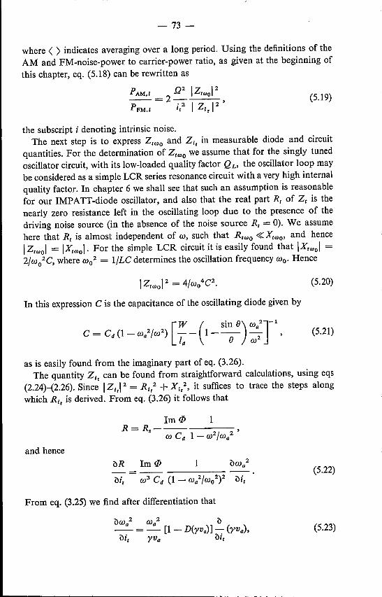
-73 -
where < > indicates averaging over a long period. Using the definitions of theAM and FM-noise-power to carrier-power ratio, as given at the beginning ofthis chapter, eq. (5.18) can be rewritten as
PAM.I Q2 1Z'QlOl2--=2----PFM•I i/ 1 ZI,12'
(5.19)
the subscript i denoting intrinsic noise.The next step is to express ZtQlO and ZI, in measurable diode and circuit
quantities. For the determination of Z'QlO we assume that for the singly tunedoscillator circuit, with its low-loaded quality factor QL, the oscillator loop maybe considered as a simple LCR series resonance circuit with a very high internalquality factor. In chapter 6 we shall see that such an assumption is reasonablefor our IMPATT-diode oscillator, and also that the real part R,of Z, is thenearly zero resistance left in the oscillating loop due to the presence of thedriving noise source (in the absence of the noise source R, = 0). We assumehere that R, is almost independent of w, such that R'QlO «XtQlO' and hence1Z'Qlol = IX'Qlol· For the simple LCR circuit it is easily found that IX'Qlol =2/w
02C, where W0
2 = I/LC determines the oscillation frequency WO' Hence
(5.20)
In this expression C is the capacitance of the oscillating diode given by
[w ( sin 8) W 2J-1
C = Cd (1- w//(2) 1;- 1--8- wa2 (5.21)
as is easily found from the imaginary part of eq. (3.26).The quantity ZI, can be found from straightforward calculations, using eqs
(2.24)-(2.26). Since 1Z 1,12 = RI,2 + XI,2, it suffices to trace the steps alongwhich RI, is derived. From eq. (3.26) it follows that
Im if> 1R=Rs--- ,
W Cd l-w2/w/and hence
?JR lm if> 1(5.22)-=--------
From eq. (3.25) we find after differentiation that
?Jw 2 W 2 ?J_a = _a [1- D(rv.)] - (yva),?Ji, rVa ?Ji,
(5.23)
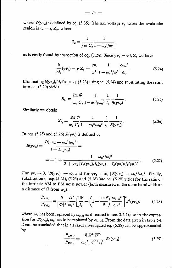
-74-
where D(yva) is defined by eq. (3.35). The a.c. voltage Va across the avalancheregion is Va= it Za>where
1 1Za=-- ,
j W Ca 1- w//w2
as is easily found by inspection of eq. (3.24). Since YVa = Y it Za we have
(5.24)
Eliminating b(yva)/bit from eq. (5.23) using eq. (5.24) and substituting the resultinto eq. (5.20) yields
ImÇp 1 1 1RI = ----.
t Wo Cd l-wa2/wo2 it B(yva)(5.25)
Similarly we obtain
Re çp 1 1 1XI =-- ----.
t Wo Cd 1 - Wa2/wo2 it B(yva)(5.26)
In eqs (5.25) and (5.26) B(yva) is defined by
D(yva) - wo2/Wa2B(yva) = 1_ D(yva)
For yva"""* 0, IB(yva)I """* 00, and for yva"""* 00, IB(yva)I """* W02/w/. Finally,
substitution of eqs (5.21), (5.25) and (5.26) into eq. (5.20) yields for the ratio ofthe intrinsic AM to FM noise power (both measured in the same bandwidth ata distance of Q from wo):
PAM,I 8 Q2 [W ( sin (J)wa,st2 J2 2--=1rti.12-2 -- 1--(J- --2 B (yva),PFM,I 'Y Wo Id Wo
(5.28)
where Wahas been replaced by Wa,st as discussed in sec. 3.2.2 (also in the expres-sion for B(yva), Wahas to be replaced by wa,st). From the data given in table 5-1it can be concluded that in all cases investigated eq. (5.28) can be approximatedby
PAM,I 8 Q2 W2- B2(yV)-P - 2Iml21 2 a •
FM,I Wo 'Y d(5.29)
-75 -
Figure 5.5shows an example of the ratio P AM.dPFM.1 as a function of YVa fordiode no. 2 in table 5-1.The ratio was calculated from eq. (5.28) for three valuesof the ratio Wa.5t2/w02. Note that in sec. 3.2.3 in the case of Wa.5t2/w02 theRVM found experimentally is given by (yva)mox = 1·8. For YVa ---+ 0 the ratioP AM.dPFM.1 ---+ co is as expected, since at "zero" output power the only"signal" left are the amplitude fluctuations of the bias current.Experimental and theoretical results of PAM.dPFM•1 as a function of the
modulation depth are presented in fig. 5.6 for diodes no. 7 and no. 14 of table
0-48-8~~------~~~--~2--_J-rVa
Fig. 5.5. The ratio PAM.,/PFM•1 as a function of yv. for diode no. 2 in table 5-1. The ratio iscalculated for ooa.5t2/oo02 equal to 0'12, 0-24 and 0'48, respectively. In the case ooa.5t2/oo02 =0-24, the RVM found experimentaIly is given by (yv.}mnx = 1·8.
-m
Fig. 5.6. Experimental and theoretical results for the ratio of the intrinsic AM to FM noisepower as a function of the modulation depth for the Si n" -p diode no. 7 and the n-GaAs S.B.diode no. 14 in table 5-1. For m < mm.x the theoretical curves were calculated from eq. (5.28),for In > mm nx from eqs (5.19) and (5.20).
5-1(as will be shown in sec. 7.2 the up-converted and down-converted noise canbe made negligibly small compared to the intrinsic noise). The modulationdepth m, defined by eq. (3.37), was chosen as abscissa because this parametercan be determined experimentally for all signal levels, whereas YVa can-only bedetermined within the RVM of the diode. The maximum modulation depthmm.x within the RVM of the diode is indicated in the figure. The theoreticalcurves were calculated from eq. (5.28) for m ~ mm.x and from eqs (5.19) and(5.20) for m ~mox' The procedure by which the results given in fig. 5.6 wereobtained for m ~ mmox will be described in sec. 6.3. In the case m ~ mmox thevalues of 1z,,1 and 1Z'oool were obtained from results oflarge-signal-impedance

(5.30)
-76 -
measurements as described in sec. 3.2.4. An example of these impedance datahas been given in figs 3.16 and 3.17.
We conclude from fig. 5.6 that for all values of m there is good agreementbetween theory and experiment. For m ~ mmax this also implies an experimentalverification of parts of the theory given in refs 12' and 65. Furthermore, theassumption that our circuit may be considered as a simple LCR circuit seemstobe correct.
5.4.3. Up-converted and down-converted oscillator noise
The influence of bias-current noise on the oscillator noise (up-conversion),and the reverse effect, the influence of oscillator noise on the bias-current noise(down-conversion), will briefly be discussed next, starting from eq. (5.15). Insec. 7.2 these types of noise will be discussed on the basis of our diode model,and a comparison with the experiments will be made in that section too.lt has already been concluded from eq. (5.15) that in our model there is no
up-conversion of bias-current noise into FM oscillator noise. Since the outputpower very much depends on the bias current we may expect that up-convertedAM oscillator noise can be present. We shall derive an expression for the lattertype of noise first. For this purpose we need the equation for the bias-currentnoise. From eq. (5.15) we find that
In the calculation of the amount of up-converted noise we assume that in eqs(5.16) and (5.30) the first term on the right-hand side is much smaller than thesecond term, so that
(5.31)
Note that this equation does not contain the unknown voltages ee, es and e,The next step is to calculate dit/d1eo. From eqs (5.13) and (5.14) it follows that
--=---- (5.32)
The calculation of bW//bit follows after elimination of b(yva)/bit from eqs(5.23) and (5.24) to be given by
bw 2 w2( W 2 ) 1
bi: =t; 1- ~2 B(yva)'(5.33)

-77 -
where use has been made of eq. (5.27); è:Jw//Mco can be found in a similar way.Thus first è:JWa2/Mco is expressed in terms of è:J(yva)/Mco, then è:J(yva)/Mco iscalculated and from both relations obtained è:Jwa2/Mco can be calculated. Thisprocedure yields the expression
è:Jwa2 w2 I-w//w2 w2( w/) 1 dit
--=-- 2 2+- 1--2
--,Mco Ico D(yva) - w /wa it w B(yva) dIco
(5.34)
while substitution of eqs (5.33) and (5.34) into eq. (5.32) yields
1--=------ (5.35)dIco 2 t.; 1 - D(yva)
The function [I-D(yva)]-l was already shown in fig. 3.11. The ratio of thesingle-sideband up-converted AM noise power to carrier power is given by
or, after substitution of eqs (5.31) and (5.35),
PAM," 1 1 (öIc02)-----
Pc 4 [1- D(yva)]2 Ico2
In sec. 7.2 we shall see that this equation can also be derived directly 46) fromour IMPATT-diode model, using the results obtained in secs 3.2.2 and 3.2.3.
The down-conversion of oscillator noise is governed by the factor A definedby (see eq. (5.15))
(5.36)
(5.37)
where ClVor is given by eq. (3.45), for which we shall write
ClVor = - 1;va2• (5.38)
In spite of the poor agreement between theory and experiment found for theeffect of d.c. restorage as discussed in sec. 3.2.5, we believe it to be appropriateto investigate the factor A somewhat further. From eqs (3.35), (5.24), (5.33),(5.35), (5.37) and (5.38) it can be found after straightforward calculations that
21; 1 1A = --2 --f(yva),
y t; RBt
(5.39)
where

-78 -
In fig. 5.7 the functionf(yva) is plotted for the minimum and the maximum valueof wa.st2/w02 as given in table 5-I. It is easily shown that
lim f(yva) = 2
and
( W 2). a,stlim f (YVa) = YVa 1 - --2- .
yVa .... eo Wo
4r-------~------~--~f(rva)
t ~2~f---__======:~w~~2 __stt,~_~w_uO_~~~0~'0~8___ 0.40 (1+Ar22!!.~:Jo}!! - t
1 ',---ïóöoil----------- 1 I
°0'~------~------~2--~0-rVa
Fig. 5.7. The function f(yva) describing the signal-level dependence of the down-conver-sion factor A for wa.st2/wo2 equal to 0'08 and 0,40, being the upper and lower limits ofwa.st2/wo2 in table 5-1.The function (I + A)-2 for diode no. 7 in table 5-1 has been plotted fora total bias resistance RB' = 100 and 10000, respectively.
We note that the limit for YVa -)0 0 is a constant * 0, so that A is non-zero at thestart of the oscillations. This is due to the fact that we are dealing with thederivative of <5 Vor with respect to i, and not with <5 Vor itself, which is zero at thestart of the oscillations. Also given in fig. 5.7 is the factor (1 + A)-2 for diodeno. 7 oftable 5-1, assuming C = 6.10-3 V-I, for RB' = 1000Q and RBt = 100Q.The latter value was chosen to approximate the situation RB = 0 for this diode.The value of C was estimated from fig. 3.l9b by taking the slope ofthe tangentin the origin, using eq. (3.32) and the data given in table 5-I. We conclude thatthe factor (1 + A)-2 is very close to unity even for RB' = 100Q. So we mightexpect the effect of down-conversion to be very slight for this diode even at lowvalues of the bias resistance RB' This conclusion is, of course, only valid withinthe RVM of the diode.Finally we conclude from fig. 5.7 and the data given in table 5-1 that within
the RVM of the diode eq. (5.37) can be approximated by
ellA=-4---.
y2 i: RBt
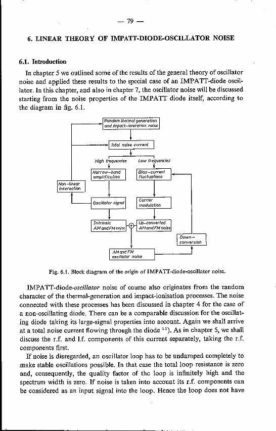
-79 -
6. LINEAR THEORY OF lMPATT-DIODE-OSCILLATOR NOISE
6.1. IntroduetionIn chapter 5 we outlined some of the results of the general theory of oscillator
noise and applied these results to the special case of an IMPATT-diode oscil-lator. In this chapter, and also in chapter 7, the oscillator noise will be discussedstarting from the noise properties of the IMPA TT diode itself, according tothe diagram in fig. 6.1.
High frequ9ncies
+Low frequencies
AM andFMoscillalor noise
Fig. 6.1. Block diagram of the origin of IMPATI-diode-oscillator noise.
IMPATT -diode-oscillator noise of course also originates from the randomcharacter of the thermal-generation and impact-ionisation processes. The noiseconnected with these processes has been discussed in chapter 4 for the case ofa non-oscillating diode. There can be a comparable discussion for the oscillat-ing diode taking its large-signal properties into account. Again we shall arriveat a total noise current flowing through the diode 11). As in chapter 5, we shalldiscuss the r.f. and IJ. components of this current separately, taking the r.f.components first.If noise is disregarded, an oscillator loop has to be undamped completely to
make stable oscillations possible. In that case the total loop resistance is zeroand, consequently, the quality factor of the loop is infinitely high and thespectrum width is zero. If noise is taken into account its r.f. components canbe considered as an input signal into the loop. Hence the loop does not have

- 80-
to be undamped completely to obtain a certain amount of output power. Theoutput signal now consists of narrow-band, amplified noise 70,80,81), and thetotalloop resistance, Rt, is slightly larger than zero. This last makes the qualityfactor Q of the loop finite. Consequently the spectrum of the output signal hasa finite width 2 Llcoo,
(6.1)
where C is the total capacitance of the oscillating diode.The "input noise" caused by the noise-generation mechanism in the IMPA TT
diode is amplified and filtered by the circuit. In this chapter we assume the signallevel so low that the output signal can be taken to consist mainly of linearlyamplified noise, while the non-linearity only enters as the mechanism ensuringthat the amount of amplification in the "noise amplifier" remains finite accord-ing to the non-linear theory described in sec. 3.2. This is the reason for callingthis chapter "Linear theory of IMPATT-diode-oscillator noise".
The linear amplification precludes the possibility of mixing products of thecomponents of the noise current itself, and of the noise current and the signalcurrent. Hence the linear theory accounts only for the intrinsic oscillator noise,i.e. the noise caused by the r.f. components of the total noise current. At highersignal levels the signal dependence of the noise generation and the influenceof the signallevelon the total noise current have to be considered more care-fully. In the diagram in fig. 6.1 this is indicated schematically by "non-linearinteraction". Non-linear oscillator noise will be discussed in chapter 7. In thatchapter the effects of up-conversion and down-conversion will be discussed,too, since these effects only arise via a non-linearity. For the discussions inthe present chapter it is sufficient to know that in the experimental situationthe conditions in the bias circuit can be chosen so as to make the effects of up-conversion and down-conversion negligible. This can be concluded from eqs(5.16) and (5.37).
Sections 6.3 and 6.4 deal with the FM and AM components of the intrinsicoscillator noise, respectively. In sec. 6.5 the possibilities of reducing oscillatornoise will be discussed. We continue now with a discussion of the width andform of the output spectrum.
6.2. Width and form of the output spectrum
By analogy with the discussion of the noise in the non-oscillating diode westart the present discussion from the Read-Langevin equation for the totalconduction current in the avalanche region
d7:1 - feCt) = fe(t) (a la - 1) + gil' (6.2)
dt
As stated in the introduetion to this chapter we assume that the signallevel is

- 81-
so low that the noise is amplified linearly. On this assumption we obtain fromeq. (6.2):
j W 7:, ine = feo ä' Vna + (2 q feo dj)1/2, (6.3)
by taking the first-order perturbation of that equation. Equation (6.3) describesthe relation between the conduction noise current ine and the noise voltage Vna
in a frequency band dj around frequency w. The difference between eq. (6.3)and the equivalent equation for the non-oscillating diode, eq. (4.10), is thateq. (6.3) describes the response to small deviations from a stationary low-leveloscillation while eq. (4.10) describes the response to small deviations from thed.c. situation. It should be emphasised that the similarity between eqs (4.10)and (6.3) only arises because we restrict ourselves to low signal levels.Along the lines as indicated at the end of sec. 4.2 we arrive at the equation
for the total noise current flowing through the diode (see also eq. (4.8)),
where Z, is the total impedance in the oscillating loop. Equation (6.4) containsthe large-signal avalanche frequency Wa as defined by eq. (3.25). As in sec. 5.4.2,we assume that for the singly tuned, low-QL circuit used the oscillator loop maybe considered as a simple LCR series resonance circuit. Then Z, reads as
Z, = R, + jx, = R, + Re + RL + Rdep1 + jwL + l/jwC, (6.5)
where R, has been decomposed according to fig. 3.10.We next assume, for thenarrow frequency range w = Wo ± Q of interest, the total loop resistance Rt,the inductance L and the capacitance C to be frequency-independent and tohave a value equal to their value at the oscillation frequency wo. From eqs (6.1)and (6.5) we then obtain
As will be clear from the introduetion to this chapter, the output power de-livered to the load resistance RL is given by
where (int2)/dj is the power-density spectrum of the total noise current givenby eq. (6.4). Via eqs (6.4) and (6.6) the factor 1+ (w - WO)2/(LJwO)2 enters
(6.6)
(6.7)

- 82-
into the integralof eq. (6.7). This factor is the only highly frequency-dependentfactor in the integration, since the quality factor Q of the almost undampedloop is very high (104 to 106), so thatLlwo is small. Taking this considerationinto account we obtain the relation
where x = (w - wo)/Llwo.For the high values of Q the value of the integralis well approximated by 'TC. After substitution we find
q 1f/J12{ [W ( Sine) w 2J( ta 2)}-1[ RRr=--2- W02Cd -- 1--- ~ 1-~ ~,(6.8)
2 7:1 Id e Wo Wo PL
where use has been made of eq. (5.21). It should be noted that PLin this
equation is still unknown, and consequently R, is still unknown. However, thevalue of PL can be obtained from the noise-free oscillator theory since we mayexpect that(a) R, is very much smaller than RL +R, + Rc, so that its effect on the value
of the impedance of the oscillating diode is negligible;(b) most of the output power is contained in a narrow frequency band around
the oscillation frequency, i.e. the centre frequency of the spectrum.For an experimental determination of Rr, P L can simply be read from a powermeter. In fig. 6.2 theoretical values of R, for 5 diodes presented in table 5-1
2
10-68·r---------~~------,14
Fig. 6.2. The totalloop resistance R, at w = Wo as a function of YVa for 5 diodes given intable 5-1. The circuit is assumed to be fixed.

- 83-
are given as a function of YVa (0 < YVa ~ (yva)max) *). The values were cal-culated using eqs (3.30), (3.32), (6.8) and the constants given in table 5-1.From fig. 6.2 we conclude that, except for extremely low values of YVa> actuallyR, «RL. Furthermore, we conclude that R, decreases with increasing signallevel, i.e. with increasing values of YVa. The latter is caused by the fact thatPL increases more than linearly with leo (note that leo and PL in eq. (6.8) arenot independent variables).
Once R, is known, we also know the halfwidth of the spectrum:
In many practical cases this equation can be approximated by
as was already discussed in connection with eq. (5.28).Making use of the relation PL = t litl2 RL' where it is the amplitude of
the r.f. current at W = Wo, we can simply write 2 Llwo = constant X leo/I itl2•From this relation we conclude that for a fixed value of leo the spectrumwidth decreases with increasing signal level. This can be understood from thediscussion given in the introduetion of this chapter. If leo is fixed the noise-excitation current is fixed. For increasing signal levels the loop has to be un-damped more and more which means that R, becomes ever smaller. Con-sequently the spectrum width decreases. Equation (6.9) will be discussed inmore detail in sec. 6.5.Figure 6.3a-f shows a series of photographs **) taken from the display screen
of a spectrum analyser (HP852A). The diode under test was diode no. 10 oftable 5-1 (RL = 5·1 0). The signal level increases going from fig. 5.3a tofig. 5.3f We conclude that the spectrum width first decreases with increasingsignal level, but then increases at higher signal levels. In fig. 6.4 we plotted thetheoretical spectrum width calculated from eq. (6.9) and the constants givenin table 5-1. We also plotted the spectrum width obtained from figs 5.3b-fSince it is impossible to determine this width directly from the photographswith any accuracy, we assumed that the spectrum can be described by a Lorentzcurve, i.e. by a curve of the form 1/(1 + x2). By so doing, the width can becalculated, for example, from the ratio ofthe noise power (in the 100-kHz band
*) The value of (yva)max concerns the range of validity of the diode model, RVM, withregard to the output power and large-signal impedance, hence not with regard to thelinear noise theory.
**)The author is indebted to H. Tjassens for making these results available.
(6.9)

c)
IcO =35mA , PL =45mW
e)
IcO = 55mA , PL = 181mW
- 84-
b)
IcO=30mA. PL =16mW
dj
f)
IcO = 70mA , PL =270mW
Fig, 6,3, The output spectrum, photographed from the display screen of a spectrum analyser,of diode no , 10 in table 5-1 (RL = 5,1 Q) for various values of the output power. Horizontalscale 1 MHzjdivision, vertical scale 10 dBydivision. Bandwidth 100 k+lz.

- 85-
2!Jfo(Hz)
t
1031,-- --'- -,,-!- __ ___j
o 100 200-PL(mW)
Fig. 6.4. Calculated half-width of the output spectrum (drawn curve) and experimental half-width (triangles) determined from the photographs given in fig. 6.3.
used) at a distance of 1MHz from the carrier to the carrier power. From fig. 6.4we conclude that at low signallevels there is good agreement between theoryand experiment. At higher signal levels the linear oscillator-noise theory isclearly no longer applicable. Figures 6.3 and 6.4 were presented mainly as anillustration. In secs 6.3 and 6.4 the linear oscillator noise will be traced moreaccurately, using the noise-measuring equipment described in sec. 5.2.The use of a Lorentz curve in the description of the output spectrum can be
accounted for as follows. In the derivation of the expression of the ratio of theintrinsic AM to FM noise power as described in sec. 5.4.2, we assumed thatfor the oscillators used the oscillator loop may be considered as a simple LCRresonance circuit. At the end of that section we found good agreement betweentheory and experiment, and concluded that the LCR-circuit representation canindeed be used. In the present chapter we also used this representation andmoreover assumed the circuit quantities to have constant values in the fre-quency band Wo ± [J of interest. These assumptions imply that in this theorythe output spectrum is .symmetrical around the frequency Wo and can be de-scribed by a Lorentz curve. If we account for the frequency dependence ofRdep1 and C, it is found from a numerical investigation that over the fre-quency range investigated, i.e. Wo ± lOOx2 Llwo the spectrum still follows aLorentz curve in a very good approximation. This is also found from experi-ments, an example of which is given in fig. 6.5. In this figure the spectrumalready presented in fig. 5.1 is shown together with a Lorentz curve fitted at200 kHz from the carrier (the deviations very close to the carrier are pre-dominantly caused by the long-term instability of the oscillator and thespectrum analyser during the writing of the spectrum).In chapter 5 we decomposed the spectrum in a carrier containing all the
output power and in upper and lower sidebands. Since the spectrum is nowknown, the relevance of this decomposition can be estimated. An example isgiven in fig. 6.6 where we plotted the output power contained in a frequency

- 86-
---Lorenfzcurve
-4.105 -2./05 0 2.105 4.105foJ9GHz---"{m(Hz)
Fig. 6.5. The output spectrum of fig. 5.1, together with a Lorentz curve fitted at Q/2n = 200kHz.
-(m(Hz)'.00;"'__ ~ _ __:1:':'.1::_0'__ 2.10'
Pdn)PL(ro)
1 0·6
2 6_n
la
Fig. 6.6. The normalised output power obtained by integration of the noise power dissipatedin the load resistance over intervals fo ± 11 (2 Llfo) as a function of 11, and as a function of/,,,= Q/2n in case 2 Llfo = 4000 Hz.
band (fo ± n Llfo), normalised to the value of the output power for n = 00.
The distance to the carrier, fm, is also indicated in the case 2 Llfo = 4 kHz.This value corresponds to Llfrms = 250 Hz in a IOO-Hz band assuming eq. (5.6)to be applicable. From fig. 6.6we conclude that the frequency bandfo ± 20 kHzalready contains more than 90% of the total output power. In the presentexample 99·4% of the total output power is contained in the frequency bandfo ± 200 kHz.
We finally emphasise that our theory for the form and width of the outputspectrum makes no pronunciation on the type of intrinsic noise involved: FM,AM or a mixture of both.

- 87-
6.3. Intrinsic FM oscillator noise
It is found experimentally that the intrinsic oscillator noise of a singly tuned,low-Ioaded-Q IMPATT-diode oscillator is predominantly FM noise. It is veryprobable that this is found because of the amplitude-limiting non-linearity ofthe diode. In figs 5.5 and 5.6 we have seen that the AM noise power is at least40 dB below the FM noise power at not too extreme low values of the signallevel. Hence it is reasonable to assume that the spectrum of the output signalis determined by the FM noise only, and to check whether this noise can actuallybe described by eq. (6.9). For the latter purpose we express the spectrum widthin terms of quantities which are more commonly used in FM-noise measure-ments, such as Ll/rms and PFM/Pc' Form eqs (5.6) and (6.9) it follows forIm ~ 2 Lilo that
q I tPI2 [W ( sin 8) W 2 J-2 I(Ll/rmsY =--2-RLdl -- 1--- ~ .z.,
47:, Id 8 Wo PL(6.10)
while eq. (5.5) states that
In these equations the noise contribution of a single sideband is considered.The conversion from Ll/rms to PFM/Pc can easily be made using fig. 6.7.
The r.m.s. frequency deviation given by eq. (6.10) does not depend onQ = 2 n/,,,. This is due to the Lorentz-curve shape of the spectrum. Theconstant Ll/rms has been found experimentally for silicon 5.82.83) and germa-nium 84) diodes. For gallium-arsenide diodes an increase of Ll/rms has beenobserved 85.86) for values of /,,, ~ 100 kHz. This effect has been attributed tothe up-conversion of a 1/1 type of noise present in these diodes 86). At firstsight this up-conversion into FM oscillator noise is in contradiction to theconclusion arrived at in sec. 5.4 that there is no up-converted FM noise. Insec. 7.2 it will be discussed that this conclusion, inferred from an idealisedmodel, has to be regarded with some reserve and that up-converted FM noisecan be present. In our experiments where /'n = 200 kHz, that is larger thanthe 100 kHz mentioned above, it is assumed tht the 1/1 type of noise whichmight be present in the GaAs diode may be neglected.It is difficult to estimate theoretically the range of validity on the linear
oscillator-noise theory. As a first check of the theory we investigated 63.87)experimentally several types of diodes at a signalleve1 such that YVa = 1, i.e.lco = 1·12 1st as follows from eq. (3.25). From table 5-1 it is known that(yva)mnx > 1 for all diodes investigated. This, of course, is a prerequisite con-dition which has to be fulfilled when one is checking the linear oscillator-noise

- 88-
-30 -40 -50
.1frms(Hz)
t
sfiT 1/
67 / 1/ 1/ / / 1/ V17 17/ V V / / Vl7 [7/ v-I/V/ V/V v-2 / / /
2[7/ 17/ 1/VV/ / V"./' 1/ ti
slY 7
67 / / / / /V/ / 1/ / / /
'V [7 V V //V// /2 / ;/ / /
V/V/ 1/VV//V/ /
/ /57 1/
:7// ////V /V///V'V V 1/ v- 1/ V/V V2/// / /vV 17/ V V V/ l/
/ / 1/ / I/, 1/1
90
-70
-8010
-lOO10
-110
-120
10 '6 8 102 2 '6 S 103
- fm (kHz)
Fig. 6.7. Conversion of PFM/Pc to Ll/rms' For example, at/m = 200 kHz, PFM/Pc = -70 dBcorresponds to Llfrms = 90 Hz, where PFM and Ll/rms are related to the same bandwidth.
theory. Results of Llfrms> experimental as well as theoretical, are presented intable 6-1. The lines along which we arrived at the data given in columns 5and 6 of table 6-1 are given schematically in fig. 6.8. The bias current at thestart of the oscillations, Isu was read from a current meter, after which thed.c. current was adjusted to 1'12 1st and the power P L was read from a powermeter. All data were substituted into eq. (6.10), and the results for Llfrms ob-tained in this way (the theoretical results), are given in the 5th column oftable 6-1. The bandwidth dfwas taken 100 Hz. In addition, we measured theratio PFM,dPc at a distance of 200 kHz from the carrier in a 100-Hz bandfollowing the procedure outlined in sec. 5.2. The experimental values of Llfrmsderived from PFM,dPc are given in the 6th column of table 6-1. In particularwhen taking into account the large number of independent measurementsneeded, comparison of the data in columns 5 and 6 leads to the conclusionthat there is good agreement between theory and experiment. So, at least atlow signal levels, the assumption that the intrinsic oscillator noise is pre-dominantly FM noise which can be described by expressing the spectrum widthin terms of the r.m.s. frequency deviation only, resulted in a good agreementbetween theory and experiment.For the Si»: -n diode no. 2, the Si n+-p diode no. 8, and the GaAs Schottky-

- 89-
TABLE 6-1
Calculated and experimentally determined r.m.s. frequency deviation of thediodes given in table 5-I. The signallevel is always chosen such that YVa = 1,i.e. Ieo = 1·12 Isl' Bandwidth df = 100 Hz; the distance to the carrier frn =200 kHz
RL PLLlf,.ms Llf,.ms e
no. type (n) (mW)calculated measured
(rad)(Hz) (Hz)
2 Sip+-n 3·1 9 414 432 1·2
(VOR = 66 V)4 Sip+-n 1·6 12 130 131 1·9
(VOR = 100 V)7 Sin+-p 0·5 7 77 58 2·3
(VOR = 111 V)10 Ge nr=p 6·8 15 265 300 1-6
(VOR = 32 V)14 n-GaAs S.B. 2·2 17 130 185 1·1
(VOR = 50V)
Measuremenls onnon - oscillaling diode
Circuil quanlities andoscillalion level
Eq. (6.10)Tableb-Icolomn5
TableG-Icolomn6
Fig. 6.8. Block diagram ofthe experimental check ofeq. (6.10). A similar diagram is applicableto eq. (6.12).
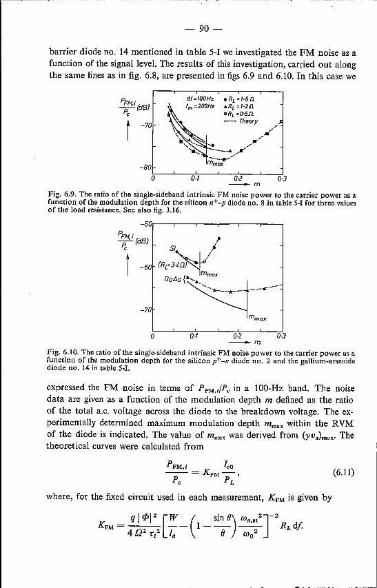
- 90-
barrier diode no. 14 mentioned in table 5-1we investigated the FM noise as afunction of the signal level. The results of this investigation, carried out alongthe same lines as in fig. 6.8, are presented in figs 6.9 and 6.10. In this case we
PFM,; (dB)Pc
t -70
-80o (J.1 0·3
-mFig. 6.9. The ratio of the single-sideband intrinsic FM noise power to the carrier power as afunction of the modulation depth for the silicon n+-p diode no. 8 in table 5-1for three valuesof the load resistance. See also fig. 3.16.
-50'~--.---.---~--.---,---,
PFfvI,; (dB)F;;
tI'
Si f(RL=3.~ .. L/
.4!l~ "1mmax
GaAS{"~'''''''' __.....'"lIl---r-- _-c
mmax
-60
-70
o 0·1 0·30·2-m
Fig. 6.10. The ratio of the single-sideband intrinsic FM noise power to the carrier power as afunction of the modulation depth for the silicon p+-n diode no. 2 and the gallium-arsenidediode no. 14 in table 5-I.
expressed the FM noise in terms of PFM,dPc in a l00-Hz band. The noisedata are given as a function of the modulation depth m defined as the ratioof the total a.c. voltage across the diode to the breakdown voltage. The ex-perimentally determined maximum modulation depth mmnx within the RVMof the diode is indicated. The value of mmax was derived from (yva)max. Thetheoretical curves were calculated from
PFM,I lco--=KFM-,Pc PL
where, for the fixed circuit used in each measurement, KFM is given by
(6.11)
qlq>12 [W ( Sine) 0) 2J-2KFM= -- 1--- ~ RLdf
4Q2-c/ Id 8 0)02

- 91-
The theoretical curves can be calculated for m :::;;;;mmax only. From figs 6.9and 6.10 we learn that all experimental curves for PFM,dPc as a function of mshow the same general behaviour. See also fig. 6.4, where 2 iJ/o is given as afunction of PL for the Ge n" -p diode no. 10. First, at low values of m, thenoise decreases with increasing m, as it should according to our linear noisetheory. Second, at high values of m, the noise increases with increasing signallevel which is in contradiction to this theory. In chapter 7 we shall see that theincrease in noise at high values of m is predominantly caused by the signaldependence ofthe total noise current which, we repeat, is assumed to be inde-pendent of the signallevel in the linear noise theory.To the author's knowledge the decreasing part of the experimental curves
has not been discussed explicitly in the literature, whereas it is this part in par-ticular that can be described by our linear theory. Cowley et al.88) have reportedthe increasing part of the curves but not the decreasing part. This is mostprobably due to their measuring method, as they measured the noise as a func-tion of the load resistance at a fixed (high) bias current and a fixed frequency.Since they did not measure up to very high values of this resistance they didnot observe the decrease in noise with increasing signallevel at low values of rn.When an estimate is made for the diode parameters needed in eq. (6.10) forthe diodes studied by Cowley et al. it is found that eq. (6.10) accounts reason-ably well for the nosie data at the highest values of the load resistance reported•by these authors.
From figs 6.9 and 6.10 we conclude that, for the diodes investigated, the linearoscillator-noise theory can be used up to a modulation depth of about 0,1,which is roughly about 30% of the maximum attainable modulation depth 47).For the gallium-arsenide diode the agreement at the lowest values of m is notas good as for the silicon diodes. We believe that deviation found for the gal-lium -arsenide diode, even at a low value of m, might be caused by the effectof diffusion of the free carriers, which was not accounted for in the analysis.As has been shown by Hulin and Goedbloed 60) the effect of carrier diffusionin gallium-arsenide diodes is much more pronounced than in silicon diodes.However, we also learn from fig. 6.10 that for the GaAs diode investigated,the deviation at low values of m is still less than 3 dB. Ithas also been found 60)that in germanium diodes the effect of carrier diffusion is pronounced. However,the determination of the experimental noise data for the germanium diode,fig. 6.4, was too crude to draw conclusions.
6.4. Intrinsic AM oscillator noise
In the foregoing section we concluded that the assumption that the spectrumwidth is predominantly caused by F.t>4noise and can be described by our ex-pression for this spectrum width led to good agreement between theory andexperiment. Consequently the linear noise theory does not provide directly for

- 92-
an expression for the intrinsic AM oscillator noise. The latter expression, how-ever, can be obtained by using results for the ratio of the intrinsic AM to FMnoise power as obtained in sec. 5.4.2. The expression for this ratio was con-firmed experimentally as valid over the whole range m ~ mmax' It is thenobvious to combine eqs (5.28) and (6.10) to an expression for the ratio of thesingle-sideband intrinsic AM noise power to carrier power
(6.12)
where B(yva) is given by eq. (5.27). We note that eq. (6.12) does not explicitlycontain the transit-time function (IJ and the ratio Wild as is the case for theFM noise. Therefore the AM noise depends much less on the transit time thanthe FM noise. Furthermore, the ratio P AM,,fPc is independent of Q, the dis-tance from the carrier, which is in agreement with experimental results reportedby Josenhans 5).
-120~M,i
Pc(dB) -130
t o D·' 0·2 0·3-m
Fig. 6.11. The ratio of the single-sideband intrinsic AM noise power to the carrier power as afunction of the modulation depth for the silicon n" -p diode no. 7 and the gallium-arsenidediode no. 14 in table 5-1. See also fig. 5.6.
In fig. 6.11 a comparison is made between theory and experiment for thesame gallium-arsenide diode as in fig. 6.10, and for the silicon n+ -p diodereported in fig. 5.6, sec. 5.4.2. The results were obtained along the same linesas sketched in fig. 6.8 for the FM noise. For the silicon diode we observe thatonce again agreement between theory and experiment is good and that thisagreement for the gallium-arsenide diode is less good, just like the FM noiseof this diode. Therefore, we believe that here, too, the diffusion of the freecarriers might play a role. But, again at low values of m the deviation is lessthan 3 dB, as it should be since the ratio PAM,,fPFM,1 for this diode agreed wellwith theory, as was shown in fig. 5.6.The intrinsic AM noise in a Read diode oscillator has been discussed by
Johnson and Robinson 89). Their expression for PAM,,fPc, eq. (10) of ref; 89,differs from our eq. (6.12), when the same conditions are considered. We be-lieve that this is due mainly to the fact that they did not take into accountthe effects of frequency and bias-current fluctuations on the admittance of the

-93 -
avalanche region (eq. (1) of ref. 89). Neglecting frequency fluctuations is notjustified since the intrinsic noise is predominantly FM noise. The bias-currentfluctuations cannot be neglected since the variations of the a.c. voltage acrossthe avalanche region are related to (r.f.) bias-current fluctuations through theavalanche frequency which is a constant for an oscillating diode in their diodemodel as well as in ours. Furthermore, if frequency fluctuations are taken intoaccount, their assumption that the sum of the load impedance and the unper-turbed diode impedance vanishes, has also to be reconsidered.
6.5. Reduction of intrinsic oscillator noise
As shown by several authors, the oscillator noise can be reduced either bycircuit techniques 75,76,82,90-92), or by injection-phase-locking techniques11,75,93,94) or by effects of harmonics'">?"). In but few papers, however,the reduction of oscillator noise is discussed starting from device param-eters 15,32,98). We shall do this in the present section for the reason that ifthe noise can be reduced by device modelling, it can be reduced further bythe other techniques mentioned above. We shall first give a brief discussion ofthe reduction of FM noise on the basis of eq. (6.10), and of the AM noise onthe basis of eq. (6.12).
Equation (6.10) reads
2 ql(1)12 [W ( Sine) wa,st2J-2 IcoRL(LIl!,) =-- -- 1-- - --dl'rms 2 e 2 'j,47:1 Id Wo PL
while from eqs (3.23), (3.24) and (3.31) it is easily derived that
(6.13)
From these equations we can draw the following conclusions:(la) The r.m.s. frequency deviation is inversely proportional to the intrinsic
response time 7:1' From fig. 4.5, where 7:1 is given as a function of the lengthof the avalanche region, we conclude that if diodes with the same length ofavalanche region are compared, the germanium and gallium-arsenide diodeshave an advantage over silicon diodes, as far as 7:1 is concerned. Using thisargument, the improvement of the noise-to-carrier ratio over silicon diodes asobserved experimentally by Rulison et al. 84) for germanium diodes and byBaranowsky et al.85) for gallium-arsenide diodes can be understood. However,as we shall see later in this section, the conclusion that germanium diodes havea better noise performance than silicon diodes 84) in general is not correct.Hence a more careful formulation of the conclusion is necessary.
(lb) The r.m.s. frequency deviation is proportional to the transit-time func-
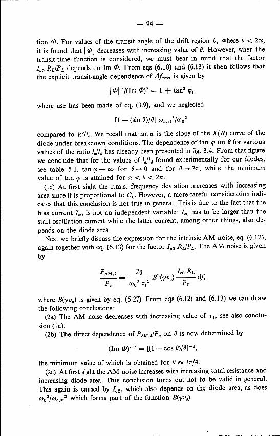
-94-
tion (j_j. For values of the transit angle of the drift region e, where ()< 2n,it is found that I (j_jl decreases with increasing value of e. However, when thetransit-time function is considered, we must bear in mind that the factorleo RL/PL depends on Im (j_j. From eqs (6.10) and (6.13) it then follows thatthe explicit transit-angle dependence of Llfrms is given by
I (j_j12 /(Im (j_j)2 = 1 + tan? cp,
where use has been made of eq. (3.9), and we neglected
[1 - (sin ())/()]wa.st2/w02
compared to W/ld. We recall that tan cp is the slope of the X(R) curve of thediode under breakdown conditions. The dependence of tan cp on e for variousvalues of the ratio la/Id has already been presented in fig. 3.4. From that figurewe conclude that for the values of la/Id found experimentally for our diodes,see table 5-1, tan cp --+ 00 for ()--+ 0 and for ()--+ 2n, while the minimumvalue of tan cp is attained for n < ()<m.(le) At first sight the r.m.s. frequency deviation increases with increasing
area since it is proportional to Co. However, a more careful consideration indi-cates that this conclusion is not true in general. This is due to the fact that thebias current leo is not an independent variable: leo has to be larger than thestart oscillation current while the latter current, among other things, also de-pends on the diode area.Next we briefly discuss the expression for the intrinsic AM noise, eq. (6.12),
again together with eq. (6.13) for the factor leo RL/PL. The AM noise is givenby
where B(yva) is given by eq. (5.27). From eqs (6.12) and (6.13) we can drawthe following conclusions:(2a) The AM noise decreases with increasing value of -r" see also conclu-
sion (la).(2b) The direct dependence of PAM.t!Pe on e is now determined by
the minimum value of which is obtained for e I:::::i 3n/4.(2c) At first sight the AM noise increases with increasing total resistance and
increasing diode area. This conclusion turns out not to be valid in general.This again is caused by leo, which also depends on the diode area, as doesw02/wa•s/ which forms part of the function B(yva).

- 95-
We next present some of the results of computer investigations of eqs (6.10)and (6.12), taking all dependent and independent variables into proper account.We shall successively answer questions how the oscillator noise can be reducedby a proper choice of the value of (1) the transit angle, (2) the junction area,and (3) the thickness of the epitaxiallayer used in the fabrication of the diodes.
Question 1What is the value of the transit angle 8 corresponding to minimum FM and
AM noise for the types of diode used in our singly tuned, low-Q oscillatorcircuit?The question is answered assuming that the following conditions are ful-
filled.(a) The output power PL is 20 mW, which is an acceptable value for the out-
put power of a local oscillator.(b) The oscillation frequency is 10 GHz.(c) The signallevel is such that YVa = 1. This value was chosen because the
results obtained in secs 6.3 and 6.4 indicate that the linear noise theorycan be used up to YVa = 1.
(d) The depletion layer is never restricted by the substrate so that the ratio Id/Wcan be assumed to be a constant for a given type of diode. The saturateddrift velocity is known from table 3-1, so that W can be calculated from8, Wo and Id/W.
(e) The diode area A = 2.10-8 m".(f) The total loss resistance R, + Rc is a constant equal to 1·3 n. This was
assumed to limit the number of variables as, strictly speaking, Rc is not aconstant 38), because the diode capacitance, which in this case is a func-tion of 8, is part of the transformer between the diode chip and the coaxialline.
(g) The values ofä' and "I needed in the calculations were assumed to be givenby
and"I ="D + pl/,
where the values of the constants p, q and "D were obtained from the ex-perimental and theoretical results discussed in chapter 4. The values ofthese constánts are listed in table 6-11.
The computer calculations were carried out along the following lines. Fromeqs (3.31) and (3.32) it follows that
W04 Ca2 ("1)2 ( Wo (RL + s,+ Re) )2PL = =- 1- RL(yva)2.
2 IX' (1- cos 8)/8 + Wo Cd (RL + R, + Re) (6.14)

- 96-
TABLE 6-11
Experimental relations for the intrinsic response time as a function of the lengthof the avalanche region: "I = "D +p laq, and for the field derivative of theaverage ionisation coefficient: (i' = p laq, see chapter 4
material/ "I (s) (i' (V-I)type "D (s) P (s m-I) q p (V-I m-I) q
Si p+-n 0.6. 10-12 1·03. 10-7 0'76 4,94.10-6 -0,75Si n+-p 0·6 . 10-12 1·03. 10-7 0·76 4.94.10-6 -0,75Gen+-p 3.4. 10-12 3.04.10-6 0·97 3,92.10-6 -0,81n-GaAs S.B. 3·2. 10-12 5.00.10-6 1·00 1·71. 10-5 -0'70
In this equation for a given value of (J, RL is now the only unknown quan-tity, since all other quantities directly follow from the conditions (a) to (g),given above. Thus RL can be solved from eq. (5.14) using an iterative cal-culation procedure. The value of wa•st
2 now follows from eq. (3.31), which,rewritten, reads
W03 (RL + Re + Rs) Cd
Wa•st2 = ---------------
(1- COS (J)/(J + Wo Cd (RL + R, + Re)(6.15)
The next step is to calculate leo from
(6.16)
This equation easily follows from eqs (3.4) and (3.30). Since all relevant diodeand circuit quantities are now known, Lt/rms and PAM. dPe can be calculated.The calculations were performed for a silicon n+ -p, a silicon p+ -n, a germa-nium n+-p, and an n-type gallium-arsenide Schottky-barrier diode, respec-tively, since for these diodes we know the value of the various diode parameters.The results of these calculations are presented in fig. 6.12.From fig. 6.12a wedraw the following conclusions for the FM noise:
(1) The r.m.s. frequency deviation shows a minimum for (J R:i 4·5 radians.Moreover, the position of the minimum is almost the same for all types ofdiodes investigated. Further investigation showed that variations of PL, A,rVa and R, + R; affected the minimum value of Llfrms but hardly affected thevalue of (J where this minimum was reached. From this we conclude that (J
is a relevant parameter along the abscissa when comparing noise properties of

- 97-
.df,ms(Hz) 102'1----\-l~:__+----_,____-J-_l
in 100Hz
t
a)
5
~CMi(dëYO ~
in 100Hz ~p
t -1400':-------':-_'~-7-G;~----,+---:-~/_L_~-=-----':-----!2 3 4 5 6 7
b) -8(rad)
Fig, 6,12, (0) The calculated r.m.s, frequency deviation, single-sideband (df = 100 Hz), as afunction of the transit angle 0 of the drift region for 4 types of diodes. The main boundaryconditions are PL = 20 mW, fo = 10 GHz, YVa = 1, A = 2.10-8 m2, R, + Rc = 1·3 n.(b) The calculated ratio of the single-sideband AM noise power to the carrier power (df =100 Hz), for the same diodes and for the same boundary conditions as given in fig. 6.120.
our oscillators equipped with diodes of various types and geometrical dimen-sions.(2) The value of Llfrms can be reduced considerably by choosing a relatively
large transit angle for the diode. In many cases the transit angle e is chosenF::j 3'Tt/4 rad, so as to optimise the output power of the oscillator. However,if not much output power is needed, and a low-noise oscillator is wanted, itis advantageous to choose a higher value of e. This conclusion is in conformitywith the experimental results presented in table 6-1.We believe that a consider-able part ofthe noise reduction found by Goldwasser et al.9!) has to be ascribedto the fact that the transit angle of the diode used was larger than tm rad, andnot only to the circuit techniques used.
(3) For a given value of e the gallium-arsenide diode has the best noise per-formance, followed by the silicon p+-11 and germanium 11+ -p diode, while thesilicon 11+ -p diode has the worst noise performance. However, for a givenlength W of the depletion layer, say 5 {Lm,the situation is completely different.This is shown in fig. 6.13 where the same values of Llfrms as in fig. 6.12a areplotted as a function of W. Comparing the results given in figs 6.12a and 6.13
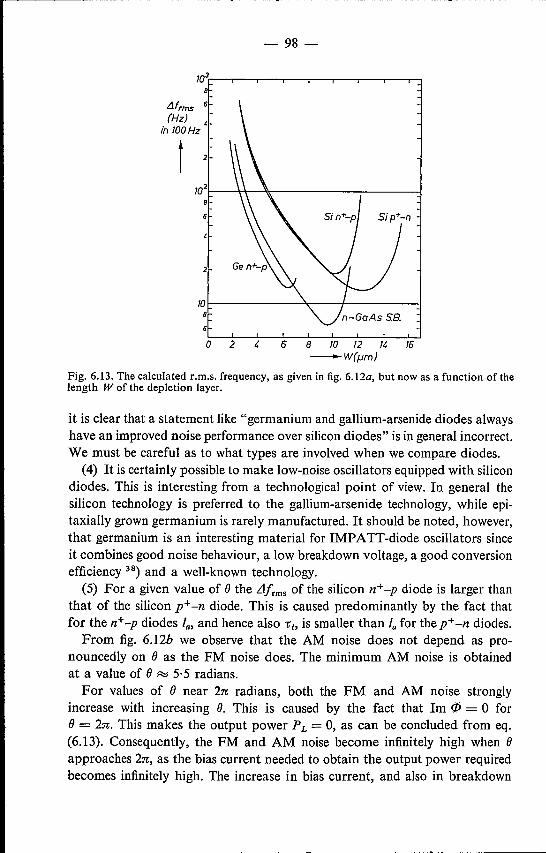
- 98-
,1frms 6
(Hz) ,in 100Hz
6
6 8 10 12 /4 16-W(fJm)
Fig. 6.13. The calculated r.m.s. frequency, as given in fig. 6.12a, but now as a function of thelength W of the depletion layer.
o 2 4
it is clear that a statement like "germanium and gallium-arsenide diodes alwayshave an improved noise performance over silicon diodes" is in general incorrect.We must be careful as to what types are involved when we compare diodes.
(4) It is certainly possible to make low-noise oscillators equipped with silicondiodes. This is interesting from a technological point of view. In general thesilicon technology is preferred to the gallium-arsenide technology, while epi-taxially grown germanium is rarely manufactured. It should be noted, however,that germanium is an interesting material for IMPATT -diode oscillators sinceit combines good noise behaviour, a low breakdown voltage, a good conversionefficiency 38) and a well-known technology.
(5) For a given value of e the L1frms of the silicon n" -p diode is larger thanthat of the silicon p+ -n diode. This is caused predominantly by the fact thatfor the n+ -p diodes IQ) and hence also "h is smaller than la for the p+ -n diodes.
From fig. 6.12b we observe that the AM noise does not depend as pro-nouncedly on e as the FM noise does. The minimum AM noise is obtainedat a value of e ~ 5·5 radians.For values of B near 2n radians, both the FM and AM noise strongly
increase with increasing e. This is caused by the fact that Im ([J = ° fore = 2n. This makes the output power PL = 0, as can be concluded from eq.(6.13). Consequently, the FM and AM noise become infinitely high when eapproaches 2n, as the bias current needed to obtain the output power requiredbecomes infinitely high. The increase in bias current, and also in breakdown
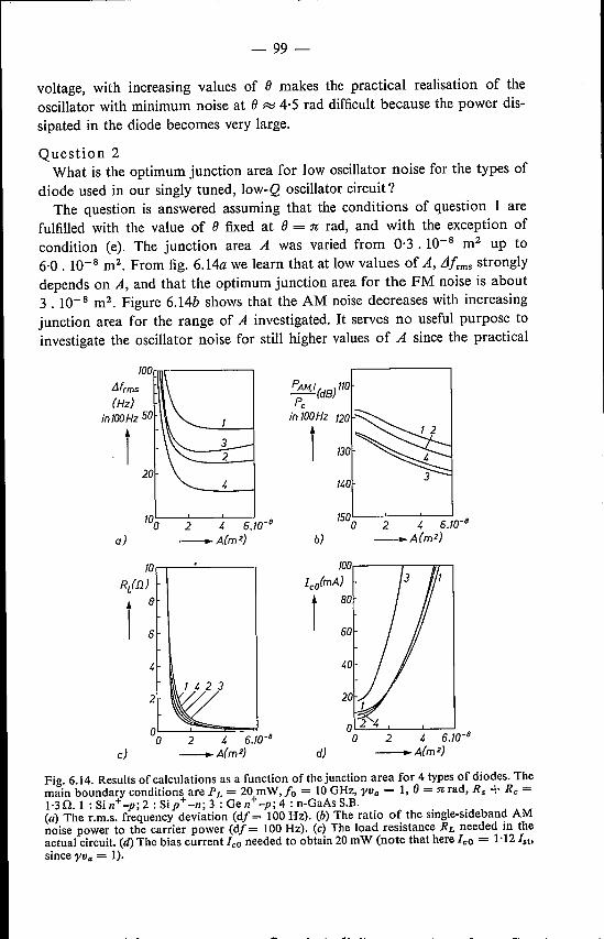
- 99-
voltage, with increasing values of e makes the practical realisation of theoscillator with minimum noise at e ~ 4·5 rad difficult because the power dis-sipated in the diode becomes very large.
Question 2What is the optimum junction area for low oscillator noise for the types of
diode used in our singly tuned, low-Q oscillator circuit?The question is answered assuming that the conditions of question 1 are
fulfilled with the value of e fixed at e = 'TC rad, and with the exception ofcondition (e). The junction area A was varied from 0·3. 10-8 m2 up to6·0. 10-8 m". From fig. 6.14a we learn that at low values of A, IJ/rms stronglydepends on A, and that the optimum junction area for the FM noise is about3. 10-8 m". Figure 6.14b shows that the AM noise decreases with increasingjunction area for the range of A investigated. It serves no useful purpose toinvestigate the oscillator noise for still higher values of A since the practical
100nnr-------,t!Jfrms
(Hz)in100Hz50
Î20
lOO 2 4 6./0-8a) _A(m2)
10.----r-_!_-----,
RL(fl)
8
Î 6
I 42 32
c)00 2 4 6./0-8
_A(m2)
PAM,; (dB) 110Pcin 100Hz
Î
Fig. 6.14. Results of calculations as a function of the junction area for 4 types of diodes. Themain boundary conditions are PL = 20 mW, Jo = 10 GHz, YVa = 1, IJ = n rad, R, + Rc =i-s ni :Sin+ -p; 2: Sip+ -n; 3: Ge /1+-p; 4: n-GaAs S.B.(a) The r.m.s. frequency deviation (dj = 100 Hz). (b) The ratio of the single-sideband AMnoise power to the carrier power (dj = lOOHz). (c) The load resistance RL needed in theactual circuit. (cl) The bias current Ico needed to obtain 20 mW (note that here lco = 1·12 Is"since YVa = 1).
11.0
1500 2 4 6./0-8b) _A{m2)
100,.------,---".,--,
IcimA)
r 80
60
40
o 2 4 6./0-8d) _A(m2)

- 100-
realisation of the oscillator must be possible. Figure 6.14c shows that the loadresistance corresponding to A = 3. 10-8 m2 is about 0·2-0'4 n, which isdifficult to realise in a practical situation. Hence this puts a restrietion on themagnitude of the junction area in practice. The power which can be dissipatedin the diode also restricts this magnitude. From fig. 6.l4d we conclude thatleo strongly increases with increasing junction area, and hence the power dis-sipated likewise.
Question 3What is the influence on the oscillator noise of the series resistance of the
"unswept" region of the epitaxiallayer, and what is the influence on the noisecaused by a restrietion of the depletion layer by the substrate?
The question is answered for a silicon /1+ -p diode with the conditions (a),(b), (c), (e) and (g) of question 1, and the conditions(h) the transit angle of the non-restricted diode is 6 = :Tl; (as in question 2);(i) the minimum loss resistance which arises from circuit losses and contact
losses is 1 n;(j) the signallevel is so low that it does not affect the value of the series resist-
ance of the unswept material 48), so that we consider the passive resistanceonly 99);
(k) in the range of interest it is assumed that a restrietion of the depletion layerby the substrate does not affect the position and shape of the avalancheregion.
The results of the calculations are given in fig. 6.15. The horizontal axis givesthe thickness of the epitaxial layer counted, in this figure, from the left-hand-side boundary of the depletion layer. The length la of the avalanche region andof the non-restricted depletion layer, Wo, are indicated. From fig. 6.15 we con-clude that for the conditions quoted the optimum FM-noise performance isfound for just punch-through of the depletion layer. Both the restrietion of thedepletion layer and the series resistance of the unswept layer give rise to anincrease in FM noise. The reverse effect is found for the AM noise.In the foregoing we tried to gain some insight into the reduction of oscillator
noise by means of a proper choice of the device parameters. As mentioned atthe beginning of this section a further reduction of the noise is possible byusing circuit techniques and/or locking techniques. For example, diode no. 7of table 5-1was placed in an oscillator circuit based on ideas put forward byKurokawa 100) *). We then obtained an output power of about 60 mW withLlfrms = 0·8 Hz (in 100 Hz at 200 kHz from the carrier), which is even slightlybetter than an X-l3 klystron 93). IMPATT-diode oscillators, in particularthose equipped with silicon diodes, have the reputation of being noisy oscil-
*) The circuit was built in our laboratory by H. Tjassens 101).

- 101-
lators. From the foregoing it might be clear that if one needs a low-noiseoscillator, one should use an IMPATT-diode oscillator.
o1.00~----."--n-~.,...-,......,.::"""'-r-~1.·0
Mrms RdD)(Hz)t 20
100'I---l-~8060
1.0a)
Fig. 6.15. Results of calculations as a function of the amount of restrietion of the depletionlayer by the substrate (x.;;;; Wo), and as a function of the length of unswept region (x > Wo),for a silicon /1+ -p diode: PL = 20 mW, fo = 10 GHz, YVa = 1, ()= 11; rad. The resistivityof the epitaxial layer was assumed to be 3·2n cm.(a) The r.m.s. frequency deviation (df = 100 Hz) and the load resistance. (b) The ratio of thesingle-sideband AM noise power to the carrier power.

- 102-
7. NON-LINEAR IMPATT-DIODE-OSCILLATOR NOISE
7.1. Introduction
In this chapter we allow for non-linear effects with regard to the oscillatornoise as distinct from the linear treatment of this noise given in the previouschapter. Therefore the present chapter deals with the dependence of the noisegeneration on the signallevel and with modulation noise (with the term modu-lation noise we denote the effectofthe r.f. noise on the IJ. noise-and the reverse,i.e. down-conversion as well as up-conversion). This type of noise was alreadytreated partly in sec. 5.4.3, where we derived expressions for it on the basis ofthe general theory of oscillator noise. The interaction of low-and high-frequencycomponents of the noise described as modulation noise should be distinguishedfrom the interaction arising from mixing of the noise at several frequencies andthe harmonics of the signal.
In sec. 7.3 the discussion is again limited to the intrinsic oscillator noise. Inthat section the difference between the measured oscillator noise and that pre-dicted by the linear noise theory will be discussed. A brief account will be givenon large-signal noise theories presented in the literature.
7.2. Modulation noise
In this section we discuss the right-hand-side branch of the diagram fig. 6.1presented in sec. 6.1, i.e. we discuss the inter-relationship between the oscillatornoise and the l.f. components of the total noise current flowing through thediode. The frequency of these components is assumed to be sufficiently low,compared with the oscillation frequency, to be thought of as bias-currentfluctuations. In the present discussion the signallevel can have any value withinthe RVM of the diodes.The connection between l.f. noise and r.f. oscillator noise, viz. up-conversion
and down-conversion, has already been discussed briefly in sec. 5.4.3. In thatsection the general theory of oscillator noise was applied to the IMPATT-diode oscillator. We there concluded that there is no up-conversion of l.f. noiseinto FM oscillator noise. This conclusion can also be obtained from eq. (3.29b)in sec. 3.2, since this equation states that the oscillation frequency is influencednei ther by the bias current nor by the signal level. In sec. 5.4.3, furthermore,an expression was derived to describe the up-conversion of IJ. noise into AMoscillator noise and, finally, we made some remarks on the down-conversionof oscillator noise. We shall continue with the effect of down-conversion first.Assuming there is no correlation between the Lr. and r.f. components of the
bias-current fluctuations, it is easily found by substitution of the intrinsic partof 6it (eq. (5.16» in eq. (5.30) that

- 103-
Substituting e = d1co/dit from eq. (5.35) gives, with Pc = t i/ RL:
P <v 2)<Mc02) = 2Ic02 [1 _ D(yva)]2 AM,l A2 + nO , (7.1
Pc RB/ (1 + A)2
where RB! = Ro + RB is the total bias-loop resistance, <vn02) = <e?) is themean-square value of the l.f-noise-voltage source in series with the diode,which is assumed to cause the IJ. noise present, and A is the factor governingthe down-conversion. A is given by eq. (5.39), and in the present discussionit is sufficient to know that A is, among other things, inversely proportionalto RBt• In sec. 5.4.3 a theoretical estimate was made of the value of (1 + A)2and it was found that this value was close to unity, even for low values of thetotal bias resistance. We shall show now that experimental evidence that(1 + A)2 ~ 1, at least within the RVM of the diode, can be obtained froma further investigation of eq. (7.1). Estimating the magnitude of the two termson the right-hand side of this equation it is found for the diodes investigatedthat eq. (7.1) is well approximated by
<M 2) _ <VnO 2)cO - R
Bt2 (1 + A)2 '
for normal values of RBt• The value of <öIc02) can be determined from thevalue of the noise voltage across the known bias resistor RB' Assuming A « 1,<vn02) can be calculated from eq. (7.2) using the experimental values of <Mc02)and Ro *). The values of <vn02) found in this way for an Si n+-p diode arepresented in fig. 7.1c. From this figure we conclude that the mean-square valueof the l.f'-noise-voltage source is independent of RB' and hence of RB! **).Since A is inversely proportional to RBr, we can conclude that (1 + A)2 ~ 1.Hence the effect of down-conversion is negligible in this case. Further investi-gations within the RVM, also using other types of diodes, have never been
*) The theory of the noise-free IMPA TT diode of chapter 3 does not provide an accurateexpression for the l.f. diode resistance Ro. Moreover the actual value of Ro is very muchinfluenced by temperature effects as was discussed in sec. 3.2.5. Hence, we have to usethe experimental value Ro (at the frequency 1,,,). The a.c. measuring current has to betaken very small in order to avoid non-linear effects via up-conversion.
**) The value of Ro is assumed to be independent of RB in order to avoid a very complicateddiode model. This assumption is supported by the experimental observations that thebias voltage, the output power and the oscillation frequency are all independent of RB'We tried to confirm the assumption experimentally, and found it to be correct within theexperimental error which, however, is rather large at low values of RB' This is the reasonwhy we made the a priori assumption of a constant Ro when RB is varied (note that Rocan vary with the signal level).
(7.2)

- 104-
-110PAM(dB)Pc
t -/20
b)
r:[~-~·~l~-~J~~~J·~lc) 10 /02 /03
-RaW)Fig. 7.1. Modulation noise of diode no. 7 in table 5-1 (Si /1+ -p, VBR = 111V) as a function ofthe bias resistance at 200 kHz. The bias current is fixed; the modulation depth is 0·09.(a) Total FM noise at 200 kHz from the carrier in a 100-Hz band. (b) Total AM noise at200 kHz from the carrier in a 100-Hz band. (c) Open-circuit noise voltage of the bias circuitat 200 kHz in a 100-Hz band.
fruitful in demonstrating experimentally the occurrence of down-conversion.A final discussion will be given at the end of this section. We now continuewith a discussion of the up-converted oscillator noise, in which we shall neglecta possible effect of down-conversion.Equation (5.36), which describes the up-conversion of the bias-current noise
into AM oscillator noise, has been obtained from an application of the generaltheory of oscillator noise. However, this equation can also be derived directlyfrom our IMPATT-diode model 46). For that purpose we combine eqs (3.33)and (3.34) to the following equation for the relative variations of the outputpower as a function of those of the bias current
(JPL 2 st.; 1 Meo 2
-P-L- = 1 - D(yva) -/-eo- + [1 - D(yvaW -Ie-02-'
where D(yva) is given by eq. (3.35). When determining noise powers the meanvalue of Meo is zero. Hence, the above equation reduces to
(7.3)

- 105-
Equation (7.3) gives the change in the average output power due to the I.f.noise current imposed on the bias current. From that equation we obtain forthe ratio of the single-sideband up-converted AM noise power to carrier power
1 1 <Mco2)4 [I-D(yva)]2 [C02
(7.4)
where PAM•u and <Mco2) have to be measured in the same bandwidth, at adistance of/,,, from the carrier and at a frequency J"" respectively. Equations(7.4) and (5.36) are identical. Assuming no correlation between the I.f. and r.f.components of the total noise current, the noise powers of the up-convertedand intrinsic noise are additive, that is
(7.5)
Furthermore, eq. (7.2) now reads
(7.6)
From eqs (7.4) and (7.6) we conclude that for a given and fixed adjustment ofthe oscillator the amount of up-converted noise can be varied by varying thebias resistance RB only. Results of experiments on a silicon n" -p diode aregiven in fig. 7.Ib, those for an n-GaAs Schottky-barrier diode in fig. 7.2. Inboth figures the theoretical curves (drawn curves) were calculated from eqs (7.4)
-110,---------...,
P...M!. (dB)Pc
yVa-----0/0·8
A"----.lI·O
~---....I1·4----..11·8----......!2·2
100 200 400 600 1000-Ra(Il)
Fig. 7.2. Total AM noise of diode no. 14 in table 5-1 (n-GaAs S.B., VBR = 50 V) as a functionof the bias resistance for several values of YVa' The noise was measured at 200 kHz from thecarrier in a 100-Hz band.

I> I' ?:ifo (2)112 !,-JO + -- Vn cos 2n lIlt,?:iVo
where (v/) is the mean-square value of the l.f.noise voltage across the diode.Assuming fo 4 = K Vo, we obtain from eqs (7.7), (7.8) and (5.5) the relation
(7.8)
-106 -
to (7.6), using the experimental values of Ro, RB and (Mc02). Theory andexperiment were fitted at RB = 1200 .Q. to obtain the value of P AM,,jPc, in allcases studied. The value of P AM,,jPC was taken independent of RB, since down-conversion is neglected. From figs 7.1b and 7.2 we conclude that the agreementbetween theory and experiment is good.Figure 7.1a shows that the FM noise really is somewhat influenced by RB'
Hence, the idealised diode model, which predicts that the FM noise does notdepend at all on the l.f. noise because it is not up-converted, has to be refined.The presence of up-converted FM noise is not quite unexpected because insec. 3.2.3 we already found a slight shift in oscillation frequency when the biascurrent was varied. If this shift is present, it automatically ensures that bias-current fluctuations are up-converted into oscillation-frequency fluctuations.The shift of the oscillation frequency could be explained by mentioning that achange of bias current causes a change in bias voltage which, in turn, variesthe cold capacitance of the diode, and consequently the oscillation frequency.It was concluded in sec. 3.2.3 and shown in fig. 3.14 that, within the RVM,the fourth power of the oscillation frequency is proportional to the d.c. voltageacross the diode. Using this conclusion, a phenomenological expression for theup-converted FM noise can be derived as follows.As is discussed in sec. 5.1, the signal frequency can be written in the form
f = fo + Llfcos (2 n!,,, t), (7.7)
where fo is the frequency of the carrier (the oscillation frequency) and áf theamplitude of the frequency deviation due to the FM noise present in the noisesideband, of width dj, at!,,, from the carrier. On the other hand, we know thatthe oscillation frequency is a function of the bias voltage. Hence, we can alsowrite
(7.9)
where, as in the case of the up-converted AM noise, we assumed that the l.f.noise is caused by a voltage source (vn02) in series with the diode. If no cor-relation is present between the intrinsic and up-converted noise, the FM noiseis given by
(7.10)

-107 -
The theoretical curve in fig. 7.Ia was calculated from eqs (7.9) and (7.10), andthe experimental values of K, Ro, RB and <Me02). The intrinsic FM noise wasdetermined in the same way as was done for the intrinsic AM noise needed ineq. (7.5). We conclude that the agreement between theory and experiment israther good *).In conclusion we remark that the up-converted noise is indeed predominantly
AM noise, which is in agreement with experimental observations made byScherer 102) and Thaler 103). It should be noted that the results given in fig. 7.1,say at RB = 10 n, that PFM.u/Pe RI 10-8 while P AM.u/Pe ~ 10-11• We thus seethat the up-converted FM noise is larger by a factor of 103 compared to theup-converted AM noise. However, since the intrinsic FM and AM noise differby a factor of 104 to 105, the up-conversion into FM noise can still be ne-glected, whereas the up-conversion into AM noise is not negligible.In the investigation of the up-converted noise it was found experimentally
that the value of <vn02) increased with the signallevelover its small-signalvalue, measured at the same value of the bias current. On the other hand itwas found that at a fixed value of the bias current, <vn02) of the oscillatingdiode did not change when the bias resistance was varied. Hence, the signaldependence of <vn02) cannot be explained by the effect of down-conversion.The increase of intrinsic AM and FM noise with respect to their values pre-dicted by the linear oscillator-noise theory of chapter 6, as is found experimen-tally, cannot be explained by a mechanism including the effect of down-con-version either. These conclusions are in contradiction with those of Weid-mann 77.78), and of Mouthaan and Rijpert 79), who concluded that the up-conversion-down-conversion loop influences the oscillator noise a great deal,even at intermediate signal levels. In our opinion this discrepancy is partlycaused by the fact they did not take into account the signal dependence of thedriving noise source, which is found to occur without the effect of modulationnoise. Hence, in this respect, their theories are small-signal theories. Moreover,they did not give a full account of the combined dependence of the diodeimpedance on Wo, [J, it and leo, as can be verified by comparing their theorieswith the oscillator-noise theory put forward by Vlaardingerbroek 12). Follow-
,*) Another origin for the up-conversion into FM noise could be the complex avalanche
frequency which was found in the extended small-signal model of the diode. In sec. 3.1.4we defined this complex avalanche frequency by the relation Wa12 = roa12 (1 - ja),where the real quantity a resulted from the extension of the diode model with respectto that summarised in sec. 2.4. If we assume the avalanche frequency to be a complexquantity in the large-signal model, too, we find from an equation equivalent to eq. (3.29)that
a = - Im g(roo)/Re g(roo).
Thus we now find that the oscillation frequency is also determined by the imaginary partof the avalanche frequency. Consequently, up-converted FM noise results if (but only if)a depends on the bias current. Unfortunately, it is not possible to obtain a theoreticalestimate of the large-signal dependence of a.

- 108-
ing our conclusions, for example, the lack of agreement between theory andexperiment at low and intermediate signallevels found in fig. 11 of ref. 79,can be understood. It should be emphasised that, with these authors, we thinkthat the up-conversion-down-conversion loop can be of importance at signallevels near the saturation of the oscillator.
7.3. Excess noise
In secs 6.3 and 6.4we concluded that with increasing signallevel the measuredintrinsic FM and AM noise becomes larger than the intrinsic noise predictedby the linear oscillator-noise theory. On the other hand, this deviation betweenexperiment and theory was not observed when the ratio of the intrinsic AMto FM noise was considered, as can be concluded from fig. 5.6. Furthermore,as already mentioned in the previous section, the 1.f. noise increases with thesignallevel with respect to its small-signal value, where this increase could notbe ascribed to the effects of modulation noise. From all those observations wedraw the conclusion that the common origin of the FM, AM and 1.f. noise,viz. the total noise current, grows with the signalleve1. In fig. 7.3 a survey ispresented of the available data for the excess noise LI(in dB) as a function ofthe modulation depth, where LI is defined by
Ll(dB)
ta)
(7.11)
la
5
o
Ll la(dB)
t 5
0
b) 0 0·1 0·2 0·3-m
Fig. 7.3. Excess noise established experimentally compared to the noise predicted by the linearnoise theory.(a) Data derived from FM-noise measurements and calculations: black triangles: Si p+-n,VBR = 66 V, RL = 3'4 n (diode no. 2 in table 5-1); black squares: Si n+-p, VBR = 111 V(diode no. 7 in table 5-1); dots: Si n+-p, VBR = 111 V, RL = 0'5 n; half-filled circles; idem,RL = 1·2n; circles: idem, RL = 1·6.Q (diode no. 8 in table 5-1); black triangles upside down:n-GaAs S.B., VBR = 50 V (diode no. 14 in table 4-1). (b) Data derived from l.f.-noise meas-urements (circles) together with the corresponding data derived from FM-noise data (dots),where black squares and triangles as under (a).

- 109-
when the FM-noise data are used, or by
(7.12)
when the l.f.-noise data are used. The data for the AM noise were not usedsince we found the ratio PAM,tlPFM,1 to be well described by the linear theory,so that these data would coincide with their corresponding FM-noise data.The theoretical value of the intrinsic FM noise was calculated from eq. (6.11)which reads
where the value of the constant KFM was obtained from the data given in table5-1, and the values of Ico and PL were obtained from meter readings. For thedata presented in fig. 7.3 we assumed the above equation to be valid for allvalues of m, so that we obtain some insight into the noise behaviour outsidethe RVM, too. The value of the small-signal l.f'-noise voltage was obtainedfrom measurements on the non-oscillating diode, since in sec. 4.5 we concludedthat the theoretical expression for this noise, eq. (4.18), could only be used ina small bias-current range. The excess-noise data obtained for the l.f. noise aregiven in fig. 7.3b, together with their corresponding FM-noise data. We con-clude from this figure that for the GaAs diode the FM and IJ. excess noisediffer a constant factor at all values of m, while the 1.f. excess noise of theSi diode at low values of m increases more rapidly than the correspondingFM noise.In spite of the "Milky Way" character of fig. 7.3, this figure clearly demon-
strates *) the increase of excess noise with the signalleve1. Furthermore, we seethat this increase is more rapid as m increases. At low values of m, diodes withpositive as well as negative values of LI (in dB) are present. We believe that thiseffect is caused predominantly by an error in the constant KFM' which valuewas derived from a number of independent measurements.
7.3.1. Discussion
In the literature, several papers have been put forward in which the large-signal noise of the IMPATT diode (used either in an oscillator or in an ampli-fier) is discussed from a theoretical standpoint. We shall now briefly discusssome aspects of these theories and compare some of the results with our ex-perimental data.
*) The data of the Si n=-p diode at the lowest values of m can be left out of considerationsince these data were obtained near the minimum power needed for a correct functioningof the noise-measuring equipment. From repeated measurements we know that an errorof ± 2 dB is then possible.

-110 -
The first large-signal noise theory was presented by Inkson 9). In his theoryhe assumes the signal level so (extremely) high that the conduction currentleaving the avalanche region can be considered as consisting of a sequence ofvery sharp pulses. When a pulse has left the avalanche region a very smallconduction current is maintained by the diode over a large part of each cycle.A new pulse builds up from this minimum current. Inkson calculated the jitterin pulse amplitude and of the interval between successive pulses due to therandom process of ionisation. From these results he calculated the AM andFM noise of the output signal. Unfortunately the sharp-pulse approximationused does not apply to the situation within the RVM of our diode model (whichis believed to be practically the same as Inkson's diode model). Within theRVM the signallevel is still too low to use this approximation, and thereforeno comparison of theory and experiment is possible. However we think thebasic idea of Inkson's theory to be correct and useful. The behaviour of theminimum current from which the pulse builds up is then of paramount impor-tance. Van Iperen 104) recently pointed out that at signal levels outside theRVM (m > mmnx) a non-negligible amount of impact ionisation occurs in thedrift region. This implies that at high signallevels the avalanche and the driftregions can no longer be treated separately. Van Iperen also pointed out thatthe ionisation in the drift region very much influences the value of the minimumcurrent in the avalanche region. We think it possible to obtain a better under-standing of the oscillator-noise behaviour outside the RVM by combining theideas set forth by Inkson and Van Iperen.Although Inkson's theory is not applicable in its present form, it nevertheless
predicts the following behaviour of the oscillator noise, which is qualitativelyin agreement with the experimental observations:(a) as the bias current is increased the output signal rapidly becomes very noisy;(b) the noise can be reduced by widening the avalanche region of the device
compared to the drift region;(c) the noise can be reduced by increasing the diode area.In the remainder of this discussion the signallevel is again restricted to signal
levels within the RVM. Furthermore, we consider the excessnoise as a functionof YVa instead of m (the ratio mlvv; for the diode investigated is given intable 7-1). Moreover, we carry out a "smoothing" procedure on the assump-tion that the excess noise is zero for YVa equal to zero, and that this noiseincreases monotonically with the signal level. The excess noise found afterapplying this procedure to the data in fig. 7.3 is given in fig. 7.4a, and indicatedby .J(yva). The value of .J(yva) was calculated from
(7.13)
The value of the correction factor LI(O)was found from the intersection of thehypothetical "smooth" curve through each series of data and the axis YVa = O.

- 111-
TABLE 7-1
Correction factor ,1(0), and the ratio of the modulation depth, m, to the nor-malised voltage across the avalanche region, YVa,as determined from experimen-tal data
no. type VBR FM/l.f. .d(0) m(yva)-1(V) (dB)
2 Sip+-n 66 FM oa 0·0597 Si «-» 111 FM 2·g 0·070
- - l.f. 0·4s Si nr=p 111 FM z-a 0·06514 n-GaAs S.B. 50 FM -2·5 0·100
The values of ,1(0) used are listed in table 7-1, where it should be noted that,1(0) is a constant for each series of excess-noise data. From fig. 7.4a we con-clude that the excess noise which follows from the FM-noise data increases forall diodes more or less in like manner with the signallevel, while those obtainedfrom the l.f.-noise data on the Si n+-p diode increase more rapidly. For com-parison, to be explained below, the graphs of I02(yva) and Io(Yva) are alsopresented in fig. 7.4.The first large-signal noise theory for arbitrary signallevel was presented by
Convert 13,105). From his theory it can be concluded that the primary noisecurrent, in our study discussed in sec. 4.2 under small-signal conditions, is nowalso proportional to I02(yva). The same conclusion can be drawn from thelarge-signal theory of Hines 17). The theories of Kuväs 14), Fikart 15) andSjölund 16) show that the primary noise current increases with the signallevelalmost proportionally with I02(yva), where the exact proportionality dependson the ratio wa//w02. The results of the theories mentioned *) are given infig. 7.4b, for the range of values of Wa12/w02 listed in table 5-1, by the shadedareas.Comparing these results with the experimental data in fig. 7.4a we find that
only the l.f. data of the Si n+-p diode vary proportionally to I02(yva). This canbe understood from the results of the large-signal noise theory of Hines 17).
His approach of the noise problem differs completely from those given inrefs 13, 14 and 15. Hines considers the influence of noise perturbations, atfrequencies Wo ± D and D, on the diode periodically driven at frequency Wo·He then carefully traces all mixing terms which arise from the non-linearbehaviour of the diode, and takes full account of the impedances of the diode
*) The theory of Sjölund is limited to values of yv. ~ 1 106).
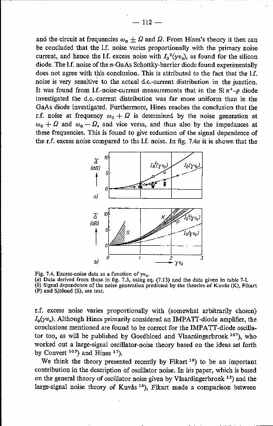
-112 -
and the circuit at frequencies Wo ± D and D. From Hines's theory it then canbe concluded that the 1.f. noise varies proportionally with the primary noisecurrent, and hence the 1.f. excess noise with I02(yva), as found for the silicondiode. The 1.f.noise ofthe n-GaAs Schottky-barrier diode found experimentallydoes not agree with this conclusion. This is attributed to the fact that the 1.f.noise is very sensitive to the actual d.c.-current distribution in the junction.It was found from l.f.-noise-current measurements that in the Si n" -p diodeinvestigated the d.c.-current distribution was far more uniform than in theGaAs diode investigated. Furthermore, Hines reaches the conclusion that ther.f. noise at frequency Wo + D is determined by the noise generation atWo + D and Wo - D, and vice versa, and thus also by the impedances atthese frequencies. This is found to give reduction of the signal dependence ofthe r.f. excess noise compared to the 1.f.noise. In fig. 7.4a it is shown that the
J"la
(dB)
t5
0a)
Lr(dB)
t0 2 3
b) -yva
Fig. 7.4. Excess-noise data as a function of YVa.(a) Data derived from those in fig. 7.3, using eq. (7.13) and the data given in table 7-1.(b) Signal dependence of the noise generation predicted by the theories of Kuväs (K), Fikart(F) and Sjölund (S), see text.
r.f. excess noise varies proportionally with (somewhat arbitrarily chosen)Io(Yva). Although Hines primarily considered an IMPATT-diode amplifier, theconclusions mentioned are found to be correct for the IMPATI-diode oscilla-tor too, as will be published by Goedbloed and Vlaardingerbroek 107), whoworked out a large-signal oscillator-noise theory based on the ideas set forthby Convert lOS) and Hines 17).
We think the theory presented recently by Fikart 16) to be an importantcontribution in the description of oscillator noise. In his paper, which is basedon the general theory of oscillator noise given by Vlaardingerbroek 12) and thelarge-signal noise theory of Kuväs 14), Fikart made a comparison between

-113 -
theory and experiment. He found good agreement at high signal levels.However, in our opinion, he compares theoryand experiment at signallevelsbeyond the RVM of his diode model, in particular where he compares histheory with the experimental data presented by Goedbloed 98). We thereforethink that the agreement between theory and experiment found could befortuitous. On the other hand, we think that Fikart's theory can lead to agood description of the oscillator noise within the RVM.

- 114-
REFERENCES
1) W. T. Read, Bell Syst. tech. J. 37, 401, 1958.2) R. L. Johnston, B. C. DeLoach and B. G. Cohen, Bell Syst. tech. J. 44, 369,1965.3) V. M. Val'd-Perlov, A. V. Krasilov and A. S. Tager, Radio Eng. Electron. Phys.
11, 1764, 1966.4) B. C. DeLoach and R. L. Johnston, Trans. IEEE EO-13, 181, 1966.5) J. J osenhans, Proc. IEEE (Lett.) 54, 1478, 1966.6) M. S. Gupta, Proc. IEEE 59, 1674, 1971.7) M. E. Hines, Int. Solid-State Circuits Conf. Dig. (Philadelphia, Pa.) 82, 1966.8) M. E. Hines, Trans. IEEE EO-13, 158, 1966.9) J. C. Inkson, Int. J. Electron. 25, 1, 1968.
10) M. T. Vlaardingerbroek, Electron. Lett. 5, 521, 1969.11) M. T. Vlaardingerbroek and J. J. Goedbloed, Philips Res. Repts 25, 452, 1970.12) M. T. Vlaardingerbroek, Electron. Lett. 7, 648, 1971.13) G. Convert, Proc. IEEE (Lett.) 59, 1266, 1971.14) R. L. Kuvas, Trans. IEEE EO-19, 220, 1972.15) A. Sjölund, Solid-State Electron. 15, 971, 1972.16) J. L. Fikart, Thesis University of Alberta, Edmonton, Canada, 1973.17) M. E. Hines, Proc. IEEE 60,1534,1972.18) J. J. Goedbloed, De Ingenieur 83, ET63, 1971 (in Dutch).19) A. S. Groove, Physics and technology ofsemiconductor devices, John Wiley and Sons
Inc., 1967, Ch. 6.20) C. B. Norris and J. F. Gibbons, Trans. IEEE EO-14, 38, 1962.21) K. G. McKay, Phys, Rev. 94, 877, 1954.22) S. M. Sze, Physics ofsemiconductor devices, John Wiley and Sons Inc., 1969, Ch. 2.23) A. G. Chynoweth, Phys. Rev. 109, 1537, 1958.24) W. Shockley, Solid-State Electron. 2,35, 1961.25) S. L. Miller, Phys. Rev. 105, 1246, 1957.26) J. E. Caroll, Hot electron microwave generators, Edward Arnold Ltd., London, Ch. 2.27) A. van der Ziel, Noise, Prentice-Hall Inc., New York, 1954, Ch. 12.28) R. B. Emmons and G. Lukovsky, Trans. IEEE EO-13, 297, 1966.29) C. A. Lee, R. L. Batdorf, W. Wiegmann and G. Kaminsky, J. appl. Phys, 38,
2787, 1967.30) S. T. Fisher, Trans. IEEE EO-14, 313, 1967.31) B. B. van Iperen, private communication.32) M. Claassen, Proc. MOGA 70 (Amsterdam, The Netherlands), Kluwer, Deventer,
The Netherlands, 1970, p. 12·26.33) R. L. Kuv äs and C. A. Lee, J. app!. Phys. 41,1743, 1970.34) G. Convert, Proc. IEEE (Lett.) 59, 1265, 1971.35) J. J. Goedbloed, Solid-State Electron. 15, 635, 1972.36) R. Hulin, M. Cia assen and W. Harth, Electron. Lett. 6, 849, 1970.37) G. A. Acket and M. T. Vlaardingerbroek, Festkörperprobleme, IX, Verlag F. Vie-
weg u. Sohn, Braunschweig, 1969, p. 280.38) B. B. van Iperen and H. Tj assens, Philips Res. Repts 27,38, 1972.39) D. de Nobel and H. G. Kock, Proc. IEEE (Lett.) 57, 2088,1969.40) R. Hulin, private communication.41) A. S. Tager, Sov. Phys. Uspekhi 9, 892, 1967.42) B. Boittiaux, E. Constant, B. Kramer, M. Lefebvre, G. Vaesken and A. Semi-
chon, Acta electronica 12, 157, 1969.43) H. K. GummeI and D. L. Scharfetter, Bell Syst, tech. J. 45, 1797, 1966.44) D. Delagebeaudeuf, L'Onde électr, 48, 722, 1968.45) M. Abramowitz and I. A. Stegun, Handbook of mathematical functions, Dover
Pub!. Inc., New York, p. 376.46) J. J. Goedbloed, Proc. MOGA 70 (Amsterdam, The Netherlands) Kluwer, Deventer,
The Netherlands, 1970, p. 12·36.47) B. B. van Iperen and H. Tjassens, Proc. MOGA 70 (Amsterdam, The Netherlands),
Kluwer, Deventer, The Netherlands, 1970, p. 7·27.48) B. B. van Iperen and H. Tjassens, Proc. IEEE (Lett.) 59,1032,1971.49) R. H. Haitz, H. L. Stover and N. J. Tolar, Trans. IEEE EO-16, 438; 1969.S0) E. Allamando, Thesis University of Lille, France, 1968.51) A. S. Tager, Sov. Phys, solid State 6, 1919, 1965.52) R. J. McIntyre, Trans. IEEE EO-13, 164,1966.

- 115-
53) M. Gilden and M. E. Hines, Trans. IEEE EO-13, 169, 1966.54) H. Melchior and W. T. Lynch, Trans. IEEE EO-13, 829, 1966.SS) H. K. Gummei and J. L. Blue, Trans. IEEE EO-14, 569, 1967.56) W. Shockley, J. A. Copeland and R. P. James, "The impedance field method of
noise calculation in active semiconductor devices", in Quantum theory of atoms,molecules and the solid state, Academic Press, 1966.
57) H. Statz, R. A. Pucel and H. A. Haus, Proc. IEEE (Lett.) 60, 645, 1972.58) T. Misawa, Solid-State Electron. 13, 1369, 1970.59) G. Persky and O. J. Bartelink, J. appl. Phys. 42,4414, 1971.60) R. Hulin and J. J. Goedbloed, Appl. Phys. Lett. 21, 69,1972.61) E. Constant, B. Kramer and L. Raczy, C. R. Acad. Sci.Paris ser. B. 265, 385,1967.62) R. H. Haitz and F. W. Voltmer, J. appl. Phys. 39, 3379,1968.63) J. J. Goedbloed, ESDERC Conference (Munich, March 1971).64) 1. M. N aq vi, J. Jap. Soc. appl. Phys. Suppl. 40, 241, 1971.65) R. L. Kuv äs and C. A. Lee, J. appl. Phys. 41, 3108, 1970.66) R. H. Haitz, J. appl. Phys. 38, 2935, 1967.67) G. Gibbons and T. Misawa, Solid-State Electron. 11, 1007,1968.68) C. R. Crowell and S. M. Sze, Appl. Phys. Lett. 9, 242, 1966.69) J. G. Ondria, Trans. IEEE MTT-16, 767, 1968.70) A. G. van Nie, Philips Res. Repts 25, 437, 1970.71) B. Schiek and J. Köhler, private communication.72) O. Schreiber and N. Hecker, Nachr. technoZ. 22, 158, 1969.73) H. P. M. Rijpert, private communication.74) K. Kurokawa, Trans. IEEE MTT-16, 234,1968.75) K. Kuroka wa, Bell Syst. techno J. 48, 1937, 1969.76) H. J. Thaler, G. Ulrich and G. Weidmann, Trans. IEEE MTT-19, 692, 1971.77) G. Weidmann, ESDERC Conference (Munich, March 1971).78) G. Weidmann, Nachr. Techn. Z. 23, 368,1970.79) K. Mouthaan and H. P. M. Rijpert, Philips Res. Repts 26, 394, 1971.80) W. A. Edson, Proc. IRE 48, 1454,1960.81) G. Klein and J. J. Zaal berg van Ze ls t, Precision electronics, Philips Technical
Library, Centrex, Eindhoven, 1967,p. 317.82) J. G. Ondria and J.-C. R. Collinet, IEEE J. solid-State Circuits SC-4, 65, 1969.83) J. R. Ashley and F. M. Palka, Proc. IEEE (Lett.) 58,155,1970.84) R. L. Rulison, G. Gibbons and J. G. Josenhans, Proc. IEEE (Lett.) 55,223,1967.85) J. J. Baranowski, V. J. Higgens, C. K. Kim and L. D. Armstrong, Microwave
J. 12, 71, 1969.86) R. Per ich on, Thesis University of Lille, France, 1971.87) J. J. Goed bloed, Electron. Lett. 7, 445, 1971.88) A. M. Cowley, Z. A. Fazarine, R. D. Hall, S. A. Hamilton, C. S. Yen and R. A.
Zettler, IEEE J. solid-State Circuits SC-5, 338, 1970.89) H. Johnson and B. B. Robinson, Proc. IEEE (Lett.)59, 1272, 1971.90) W. Harth and G. Ulrich, Electron. Lett. 5,7, 1969.91) R. E. Goldwasser, J. Berenz, C. A. Lee and G. C. Dalman, Proc. MOGA 70
(Amsterdam, The Netherlands), Kluwer, Deventer, The Netherlands, 1970, p. 12·19.92) K. Schünemann and B. Schiek, Electron. Lett. 7,659, 1971.93) M. E. Hines, J. _C.R.Collinet and J.G.Ondria, Trans. IEEE MT-16, 738,1968.94) B. Schiek and K. Schünemann, Arch. el. Übertr. 26, 310, 1972.95) A. S. Tager and A. M. Tsebiyer, Radio Eng. Electron. Phys. 14, HI0, 1969.96) R. Perichon, Trans. IEEE MTT-18, 988, 1970.97) K. Mouthaan, Philips Res. Repts 25,33,1970.98) J. J. Goedbloed, Proc. 1971 European Microwave Conference (Stockholm, Sweden),
Suppl., p. 6.99) B. B. van Iperen, H. Tjassens and J. J. Goedbloed, Proc. IEEE (Lett.) 57,1341,
1969.100) K. Kurokawa, Trans. IEEE MT-19, 793, 1971.101) H. Tjassens, Proc. 1973European Microwave Conf. (Brussels, Sept. 1973).102) E. F. Scherer, IEEE Trans. MTT-16, 781, 1968.103) H. J. Thaler, ESDERC Conference (Munich, March 1969).104) B. B. van Iperen, Proc. IEEE (Lett.), to be published.105) G. Convert, Revue Thomson-CSF 3,419, 1971.106) A. Sjölund, private communication.107) J. J. Goedbloed and M. T. Vlaardingerbroek, to be published.