microwave solid-state devices · ppt file · web view ·...
TRANSCRIPT
Microwave Solid-State Devices
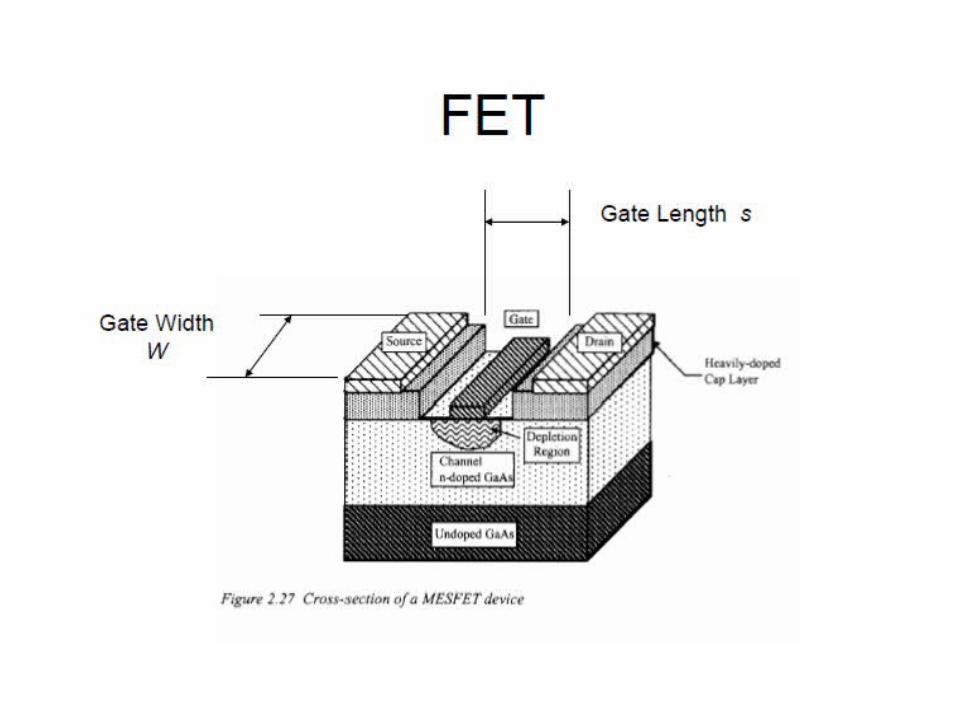
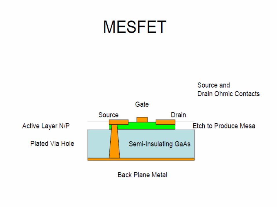
Microwave Transistors
• Designed to minimize capacitances and transit time
• NPN bipolar and N channel FETs preferred because free electrons move faster than holes
• Gallium Arsenide has greater electron mobility than silicon
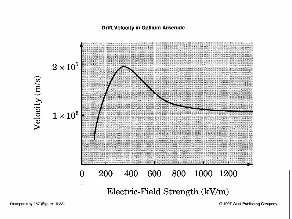
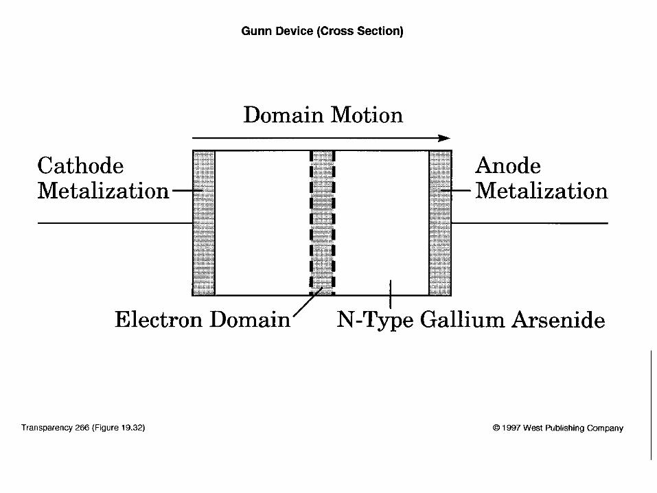
Gunn Device
• Slab of N-type GaAs (gallium arsenide)• Sometimes called Gunn diode but has no
junctions• Has a negative-resistance region where drift
velocity decreases with increased voltage• This causes a concentration of free electrons
called a domain

Transit-time Mode
• Domains move through the GaAs till they reach the positive terminal
• When domain reaches positive terminal it disappears and a new domain forms
• Pulse of current flows when domain disappears
• Period of pulses = transit time in device

Gunn Oscillator Frequency
• T=d/vT = period of oscillationd = thickness of devicev = drift velocity, about 1 105 m/s
• f = 1/T
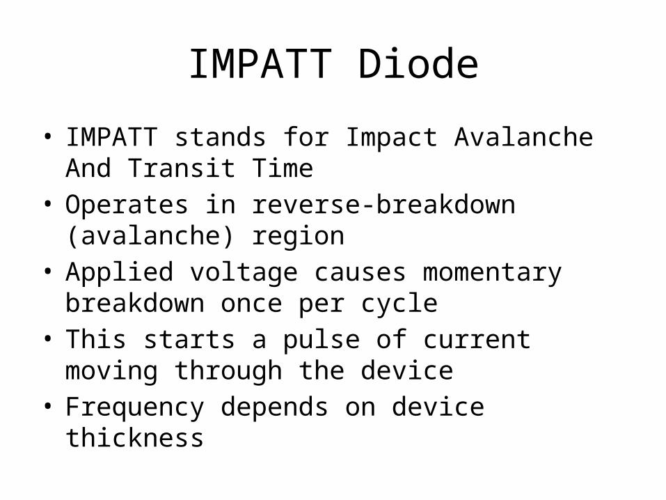
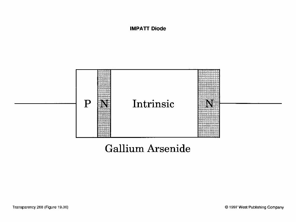
IMPATT Diode
• IMPATT stands for Impact Avalanche And Transit Time
• Operates in reverse-breakdown (avalanche) region• Applied voltage causes momentary breakdown once
per cycle• This starts a pulse of current moving through the
device• Frequency depends on device thickness
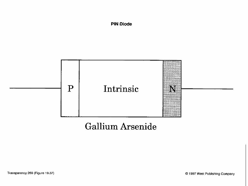
PIN Diode
• P-type --- Intrinsic --- N-type• Used as switch and attenuator• Reverse biased - off• Forward biased - partly on to on depending on
the bias
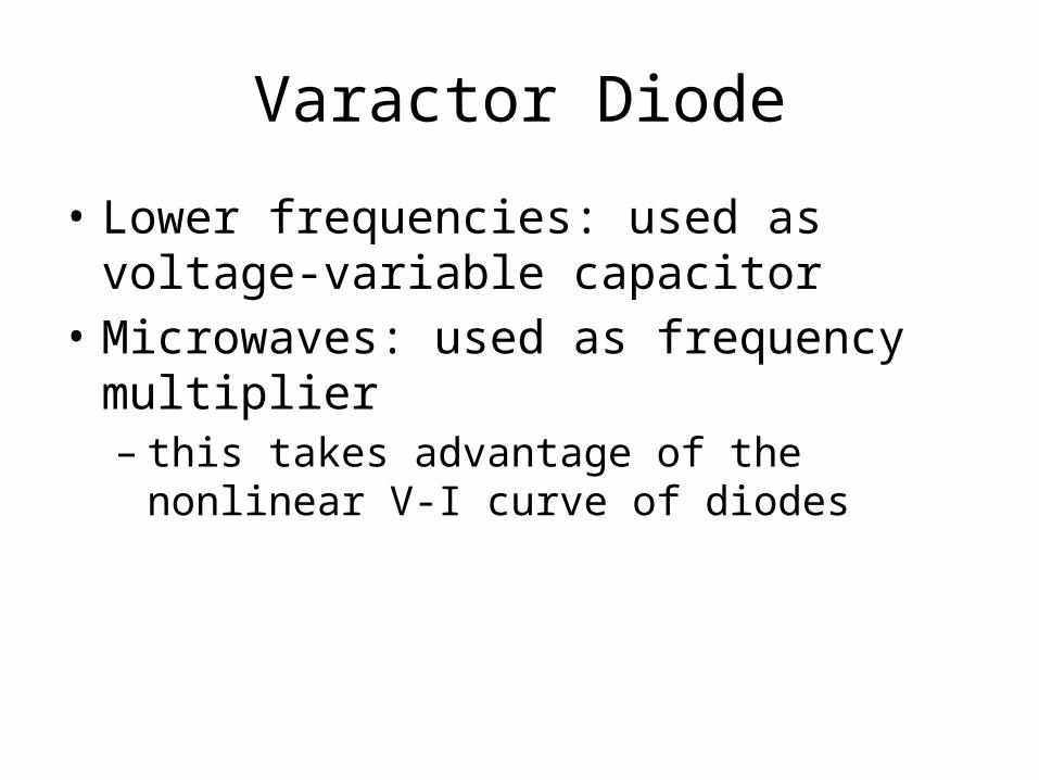
Varactor Diode
• Lower frequencies: used as voltage-variable capacitor
• Microwaves: used as frequency multiplier– this takes advantage of the nonlinear V-I curve of
diodes
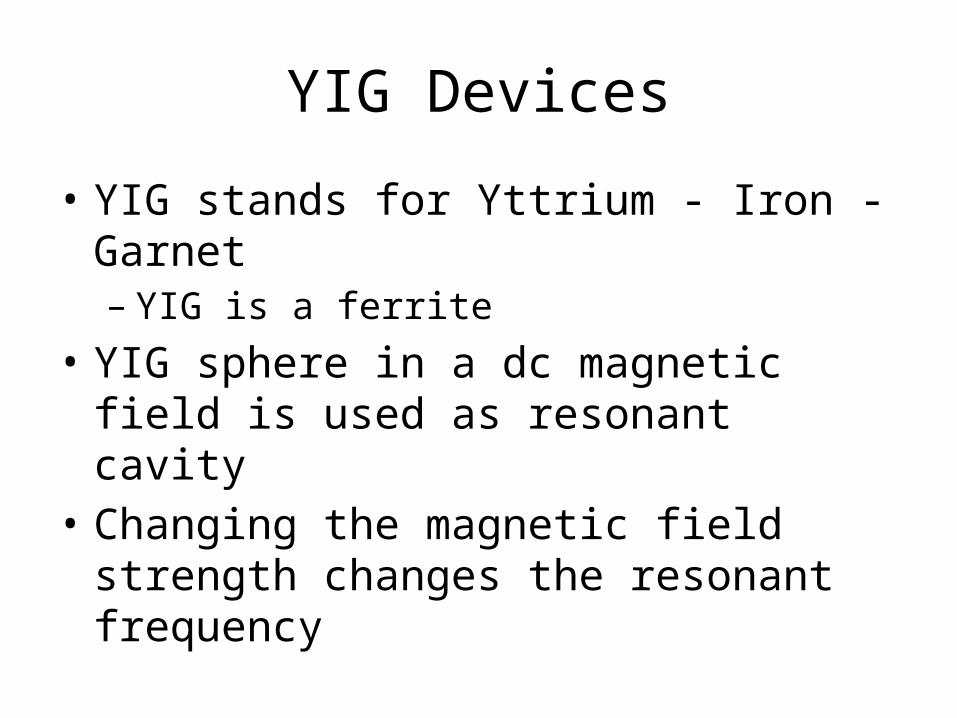
YIG Devices
• YIG stands for Yttrium - Iron - Garnet– YIG is a ferrite
• YIG sphere in a dc magnetic field is used as resonant cavity
• Changing the magnetic field strength changes the resonant frequency
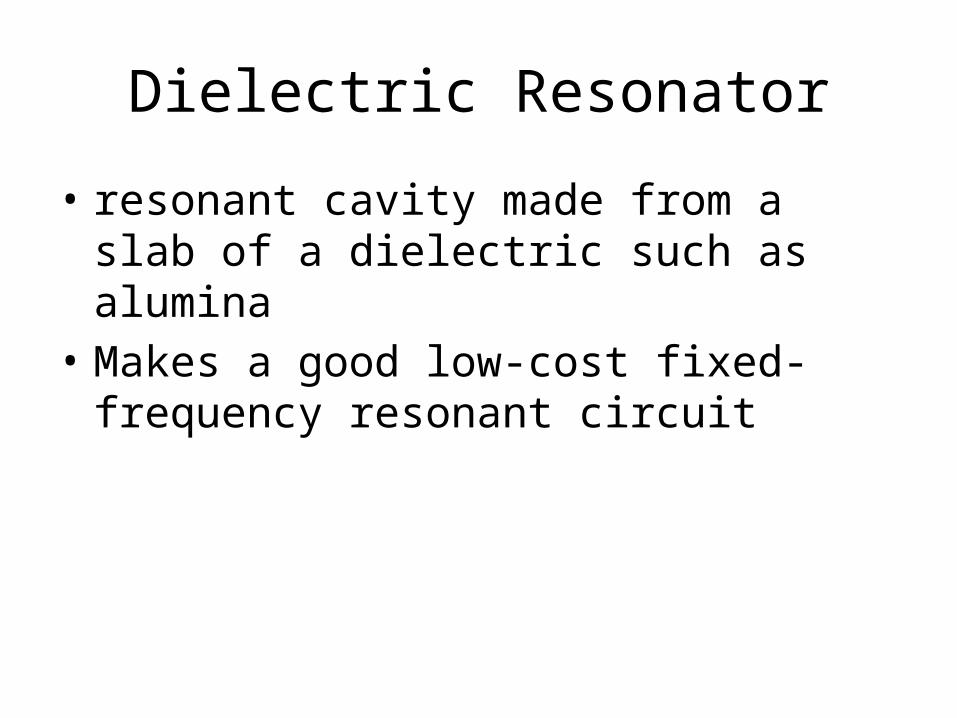
Dielectric Resonator
• resonant cavity made from a slab of a dielectric such as alumina
• Makes a good low-cost fixed-frequency resonant circuit
Microwave Tubes
• Used for high power/high frequency combination
• Tubes generate and amplify high levels of microwave power more cheaply than solid state devices
• Conventional tubes can be modified for low capacitance but specialized microwave tubes are also used
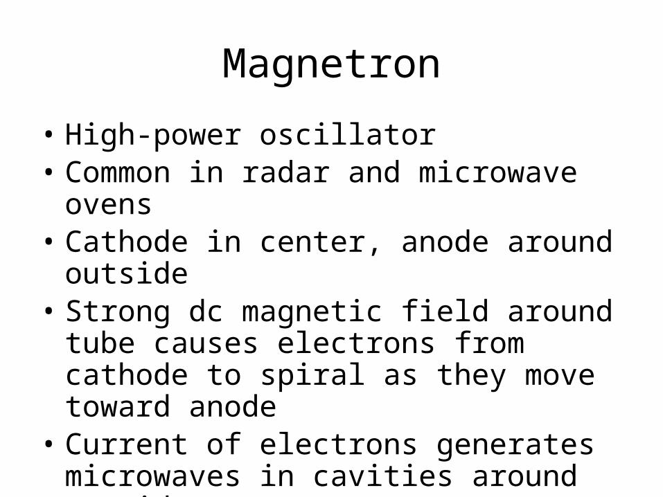
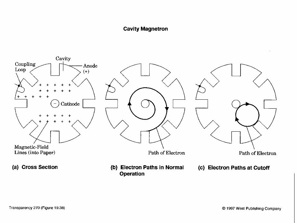
Magnetron
• High-power oscillator• Common in radar and microwave ovens• Cathode in center, anode around outside• Strong dc magnetic field around tube causes
electrons from cathode to spiral as they move toward anode
• Current of electrons generates microwaves in cavities around outside
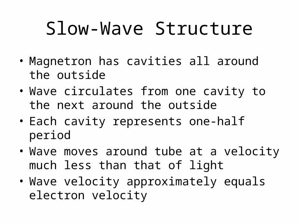
Slow-Wave Structure
• Magnetron has cavities all around the outside• Wave circulates from one cavity to the next around
the outside• Each cavity represents one-half period• Wave moves around tube at a velocity much less
than that of light• Wave velocity approximately equals electron velocity
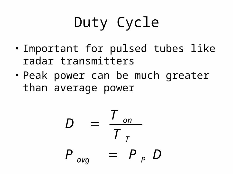
Duty Cycle
• Important for pulsed tubes like radar transmitters
• Peak power can be much greater than average power
DPPTTD
Pavg
T
on
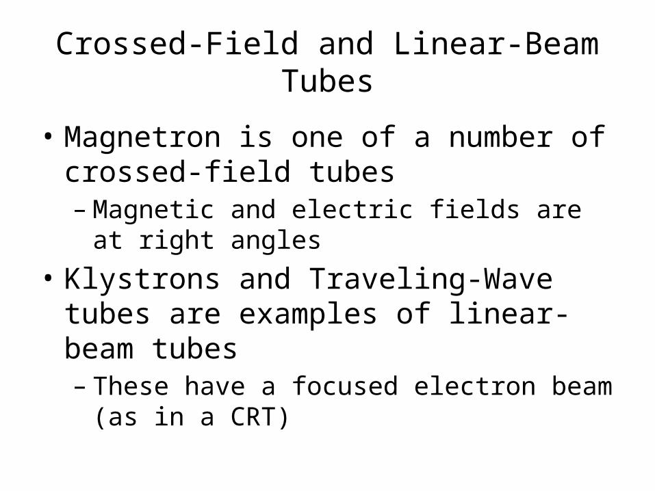
Crossed-Field and Linear-Beam Tubes
• Magnetron is one of a number of crossed-field tubes– Magnetic and electric fields are at right angles
• Klystrons and Traveling-Wave tubes are examples of linear-beam tubes– These have a focused electron beam (as in a CRT)

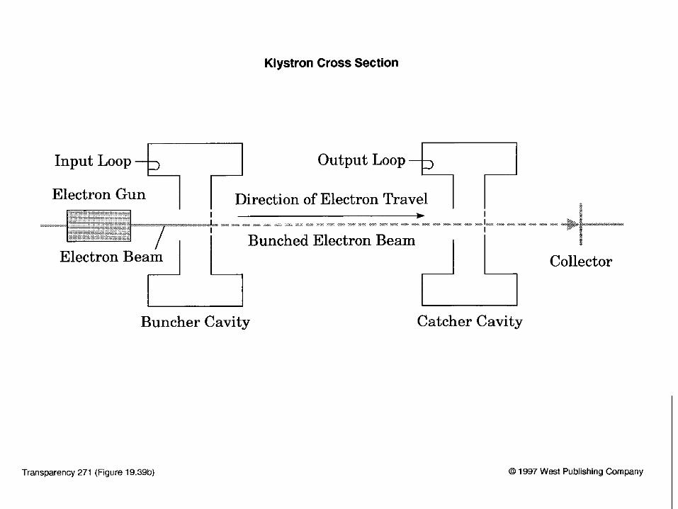
Klystron
• Used in high-power amplifiers• Electron beam moves down tube past several
cavities.• Input cavity is the buncher, output cavity is the
catcher.• Buncher modulates the velocity of the
electron beam

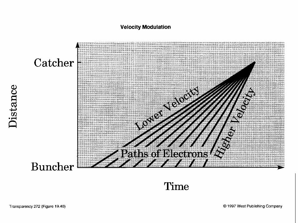
Velocity Modulation
• Electric field from microwaves at buncher alternately speeds and slows electron beam
• This causes electrons to bunch up• Electron bunches at catcher induce
microwaves with more energy • The cavities form a slow-wave structure
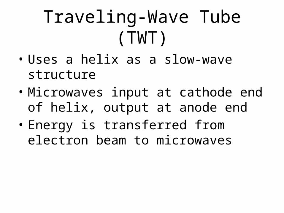
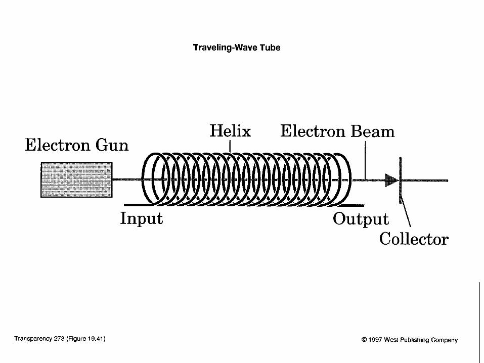
Traveling-Wave Tube (TWT)
• Uses a helix as a slow-wave structure• Microwaves input at cathode end of helix,
output at anode end• Energy is transferred from electron beam to
microwaves
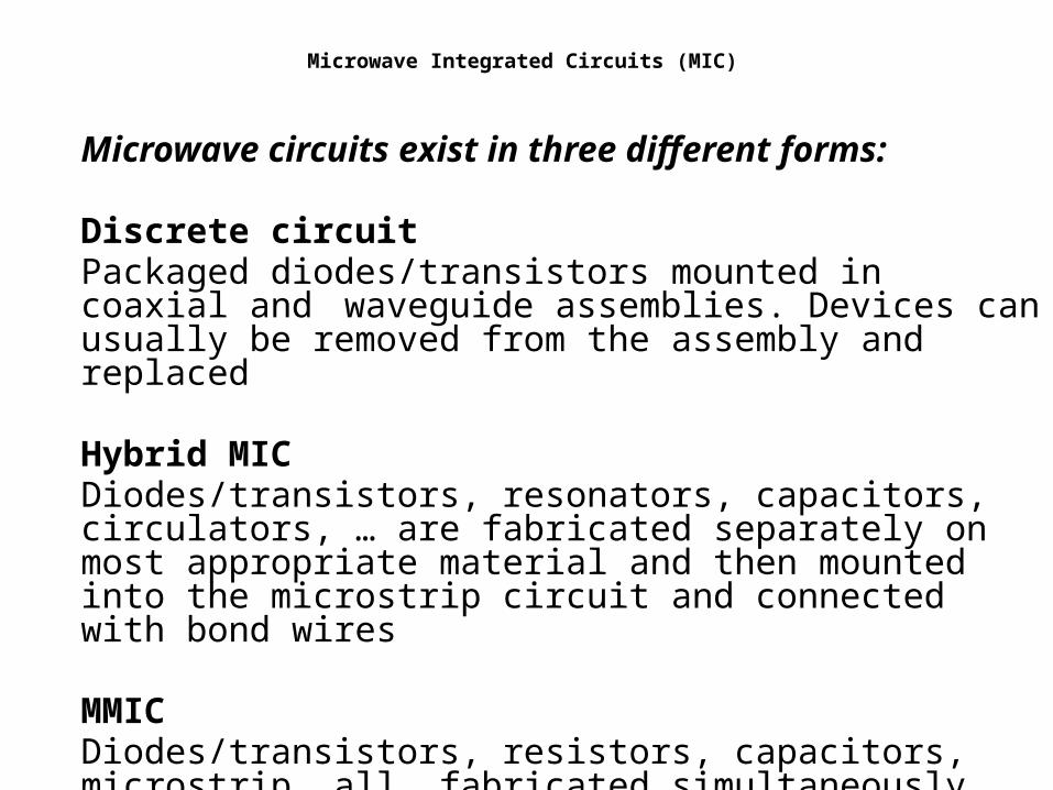
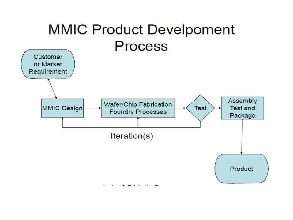
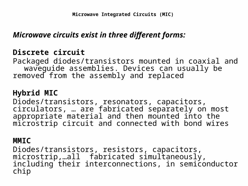
Microwave Integrated Circuits (MIC)
Microwave circuits exist in three different forms:
Discrete circuitPackaged diodes/transistors mounted in coaxial and waveguide assemblies. Devices can usually be removed from the assembly and replaced
Hybrid MICDiodes/transistors, resonators, capacitors, circulators, … are fabricated separately on most appropriate material and then mounted into the microstrip circuit and connected with bond wires
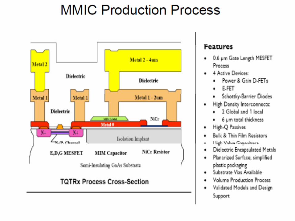
MMIC Diodes/transistors, resistors, capacitors, microstrip,…all fabricated simultaneously, including their interconnections, in semiconductor chip
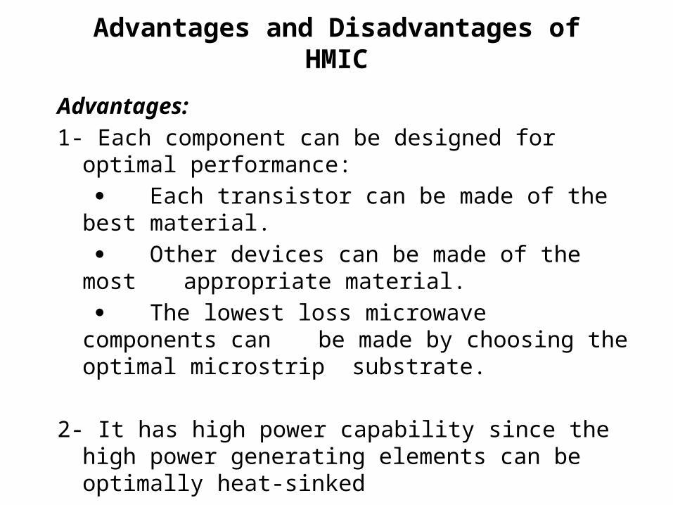
Advantages and Disadvantages of HMIC
Advantages:1- Each component can be designed for optimal performance:
Each transistor can be made of the best material. Other devices can be made of the most appropriate material. The lowest loss microwave components can be made by choosing the optimal microstrip substrate.
2- It has high power capability since the high power generating elements can be optimally heat-sinked
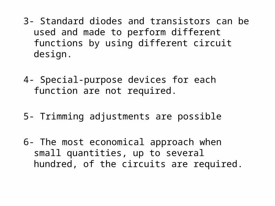
3- Standard diodes and transistors can be used and made to perform different functions by using different circuit design.
4- Special-purpose devices for each function are not
required.
5- Trimming adjustments are possible
6- The most economical approach when small quantities, up to several hundred, of the circuits are required.
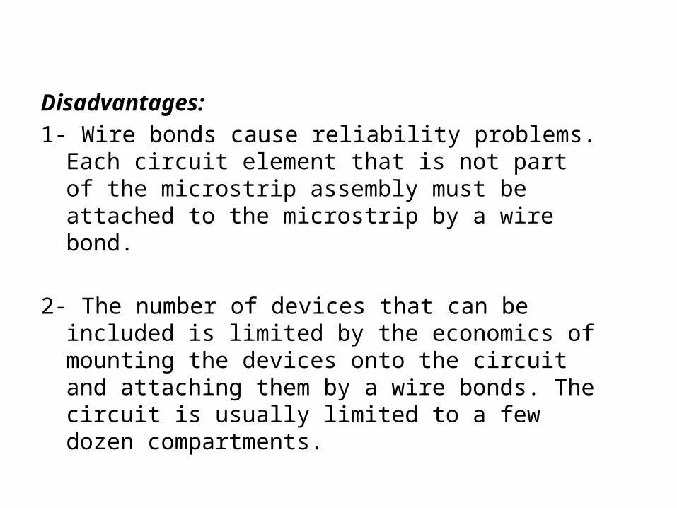
Disadvantages:1- Wire bonds cause reliability problems. Each circuit
element that is not part of the microstrip assembly must be attached to the microstrip by a wire bond.
2- The number of devices that can be included is limited by the economics of mounting the devices onto the circuit and attaching them by a wire bonds. The circuit is usually limited to a few dozen compartments.
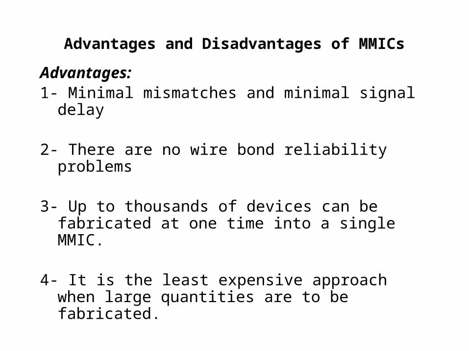
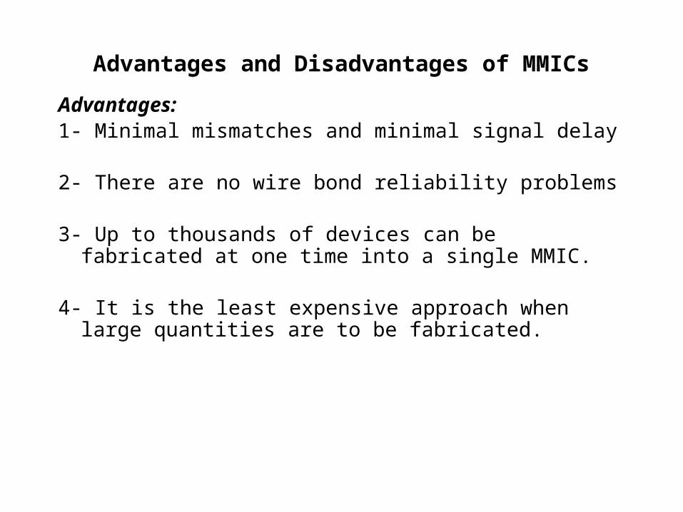
Advantages and Disadvantages of MMICs
Advantages:1- Minimal mismatches and minimal signal delay
2- There are no wire bond reliability problems
3- Up to thousands of devices can be fabricated at one time into a single MMIC.
4- It is the least expensive approach when large quantities are to be fabricated.
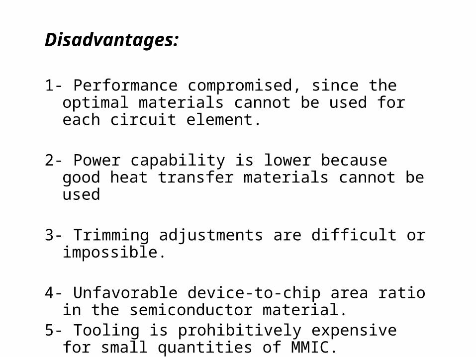
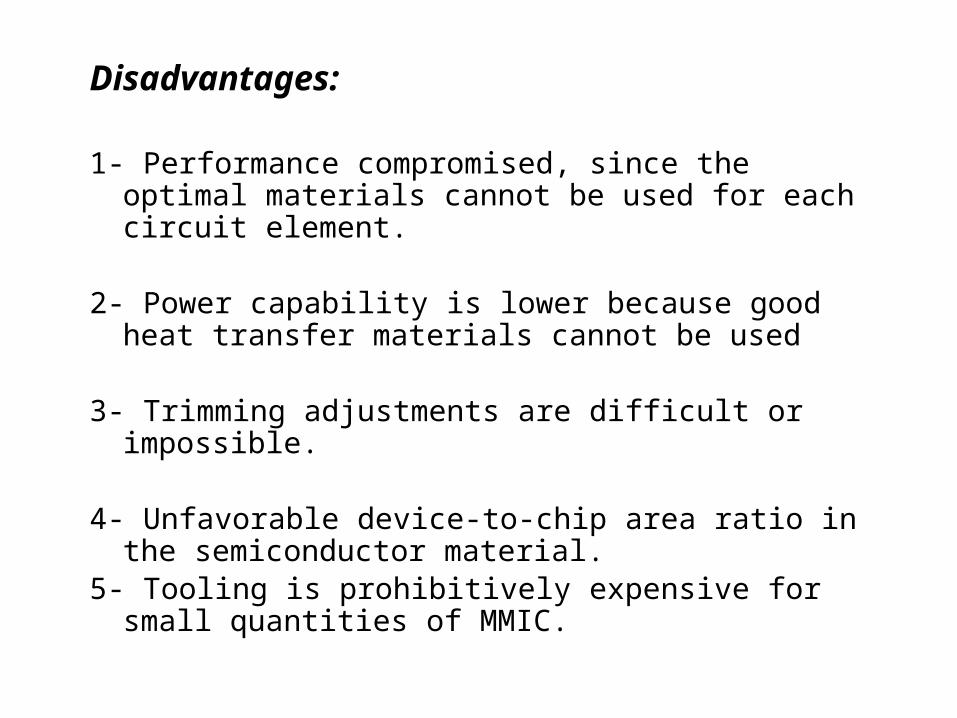
Disadvantages:
1- Performance compromised, since the optimal materials cannot be used for each circuit element.
2- Power capability is lower because good heat transfer materials cannot be used
3- Trimming adjustments are difficult or impossible.
4- Unfavorable device-to-chip area ratio in the semiconductor material.
5- Tooling is prohibitively expensive for small quantities of MMIC.
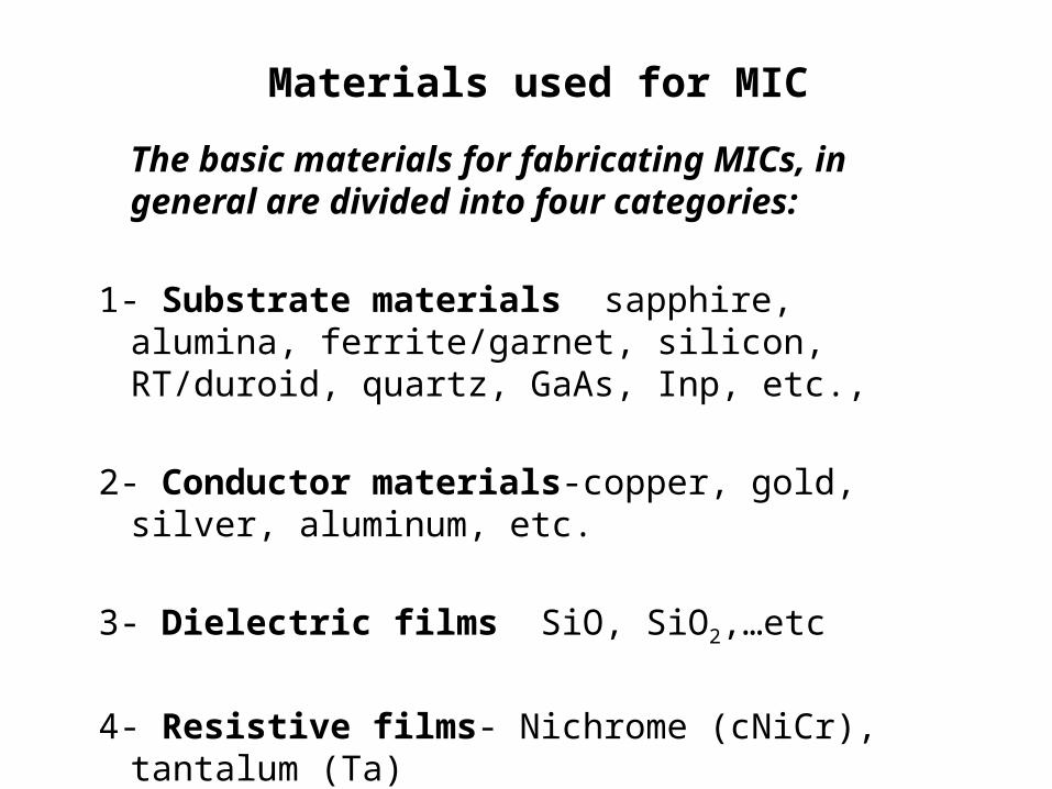
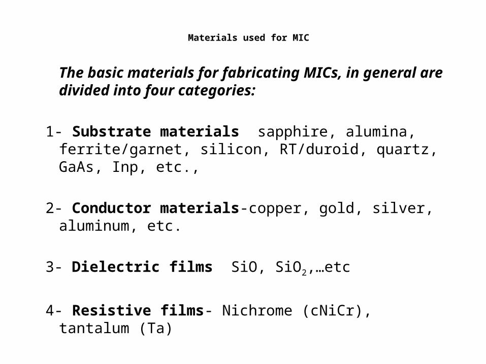
Materials used for MIC
The basic materials for fabricating MICs, in general are divided into four categories:
1- Substrate materials sapphire, alumina, ferrite/garnet, silicon, RT/duroid, quartz, GaAs, Inp, etc.,
2- Conductor materials-copper, gold, silver, aluminum, etc.
3- Dielectric films SiO, SiO2,…etc
4- Resistive films- Nichrome (cNiCr), tantalum (Ta)
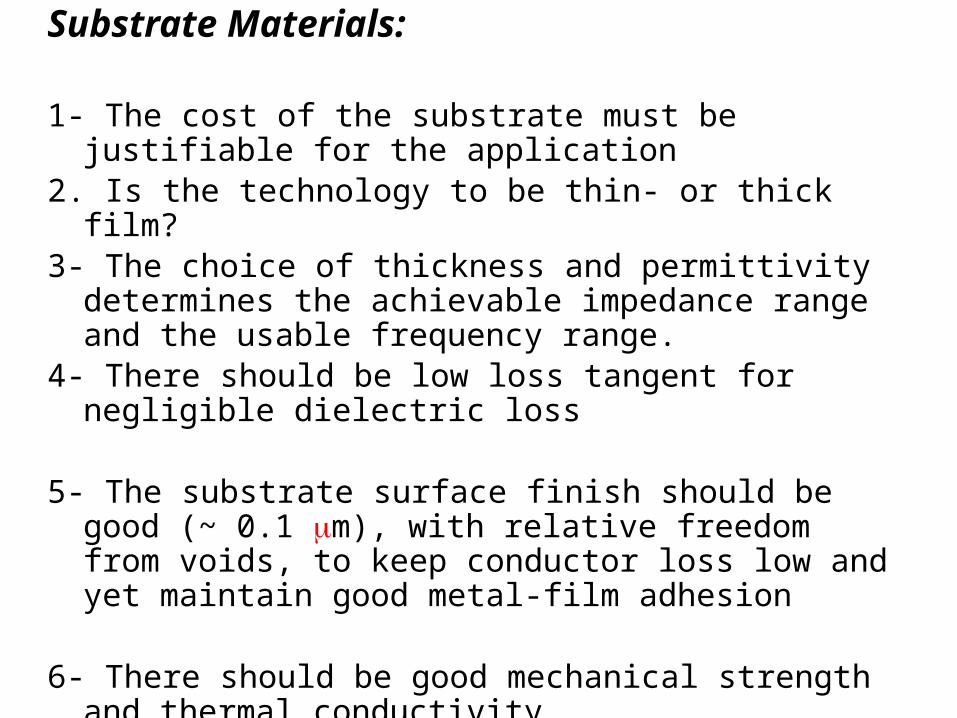
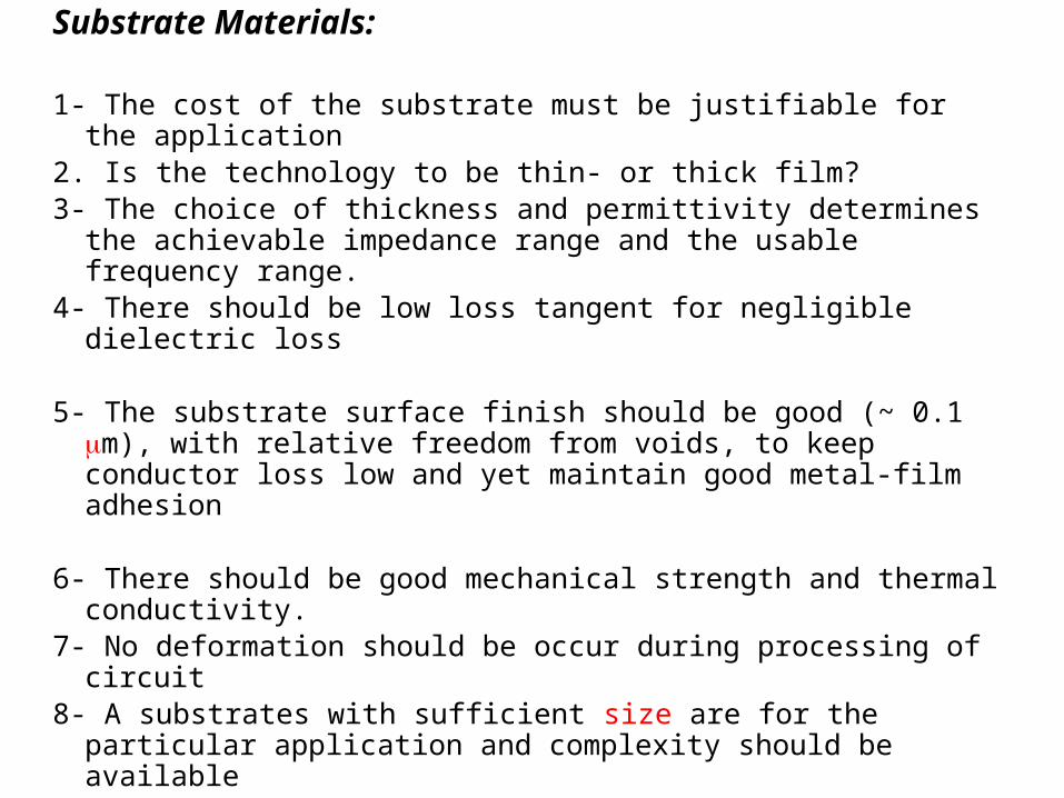
Substrate Materials:
1- The cost of the substrate must be justifiable for the application2. Is the technology to be thin- or thick film?3- The choice of thickness and permittivity determines the
achievable impedance range and the usable frequency range.4- There should be low loss tangent for negligible dielectric loss
5- The substrate surface finish should be good (~ 0.1 mm), with relative freedom from voids, to keep conductor loss low and yet maintain good metal-film adhesion
6- There should be good mechanical strength and thermal conductivity.
7- No deformation should be occur during processing of circuit8- A substrates with sufficient size are for the particular
application and complexity should be available
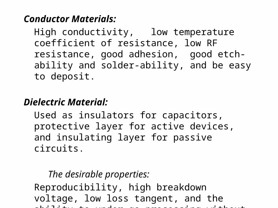
Conductor Materials: High conductivity, low temperature coefficient of resistance, low RF resistance, good adhesion, good etch- ability and solder-ability, and be easy to deposit.
Dielectric Material:Used as insulators for capacitors, protective layer for active devices, and insulating layer for passive circuits.
The desirable properties: Reproducibility, high breakdown voltage, low loss tangent, and the ability to under go processing without developing pin holes
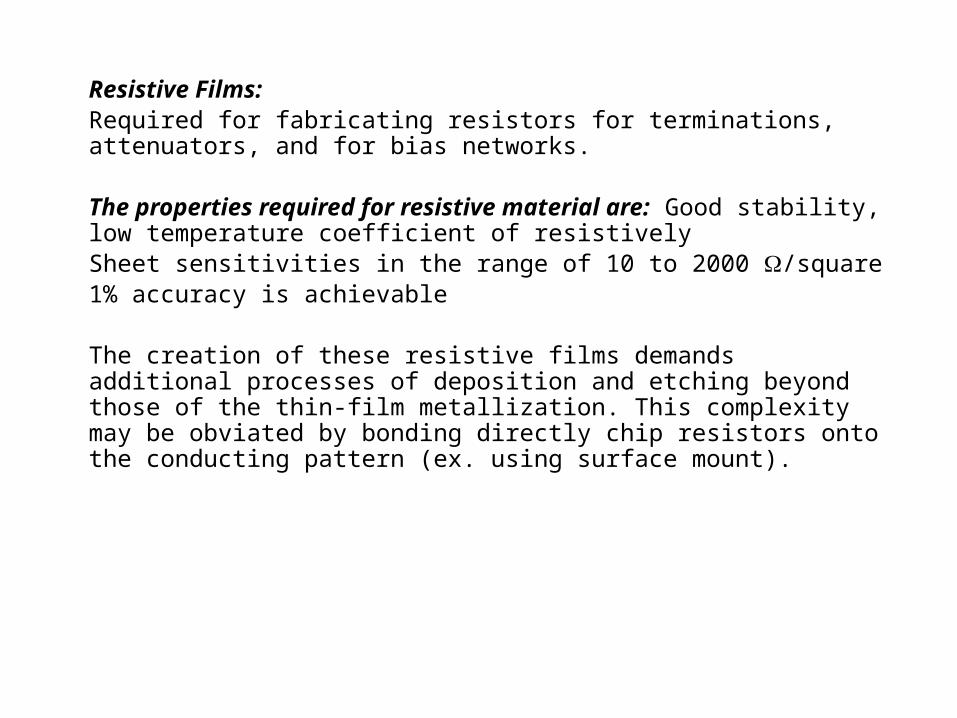
Resistive Films:Required for fabricating resistors for terminations, attenuators, and for bias networks.
The properties required for resistive material are: Good stability, low temperature coefficient of resistivelySheet sensitivities in the range of 10 to 2000 W/square1% accuracy is achievable
The creation of these resistive films demands additional processes of deposition and etching beyond those of the thin-film metallization. This complexity may be obviated by bonding directly chip resistors onto the conducting pattern (ex. using surface mount).
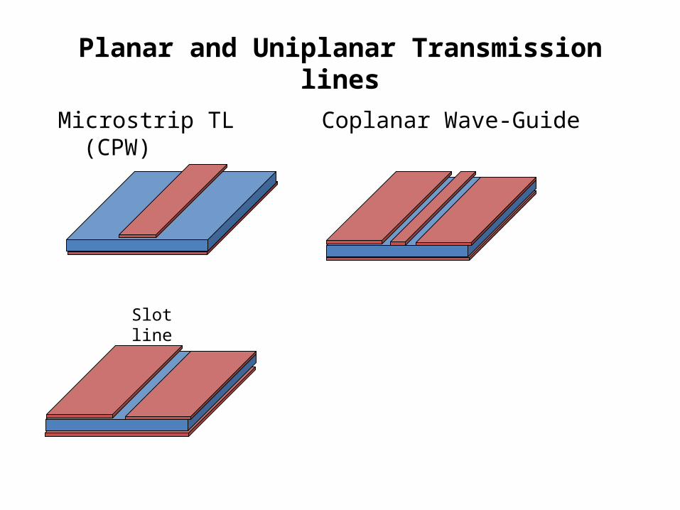
Planar and Uniplanar Transmission lines
Microstrip TL Coplanar Wave-Guide (CPW)
Slot line
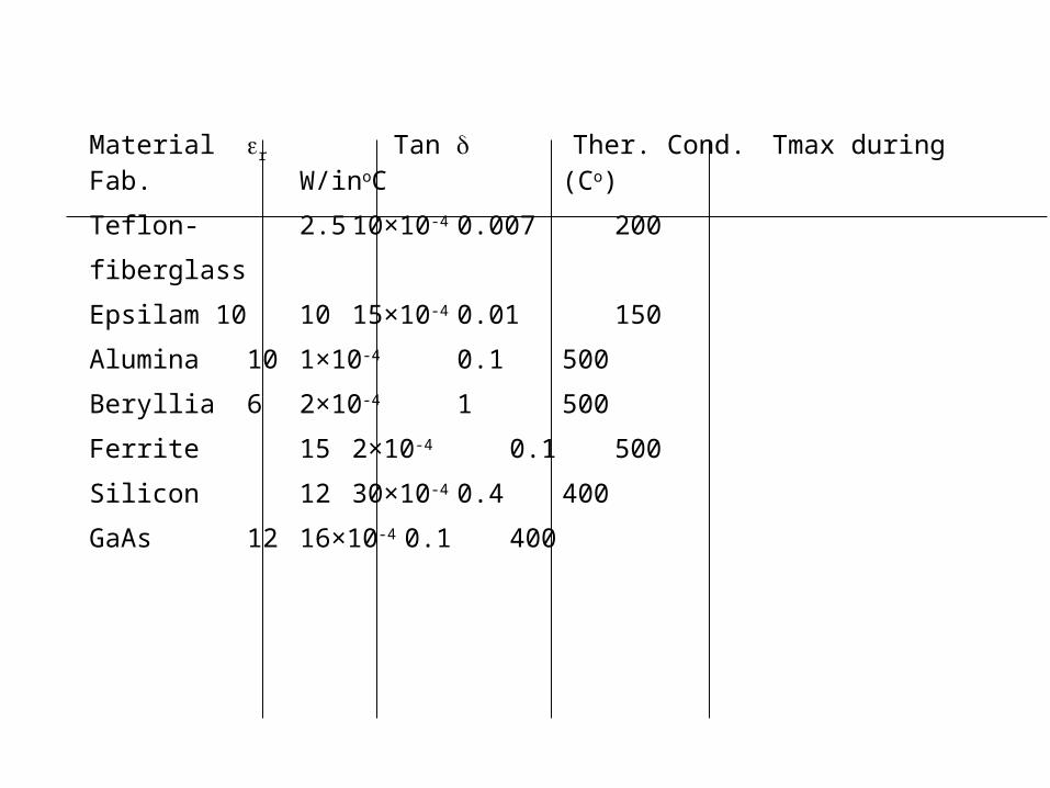
Material er Tan d Ther. Cond. Tmax during Fab. W/inoC (Co)
Teflon- 2.5 10×10-4 0.007 200
fiberglass
Epsilam 10 10 15×10-4 0.01 150
Alumina 10 1×10⁻⁴ 0.1 500
Beryllia 6 2×10⁻⁴ 1 500
Ferrite 15 2×10⁻⁴ 0.1 500
Silicon 12 30×10-4 0.4 400
GaAs 12 16×10-4 0.1 400
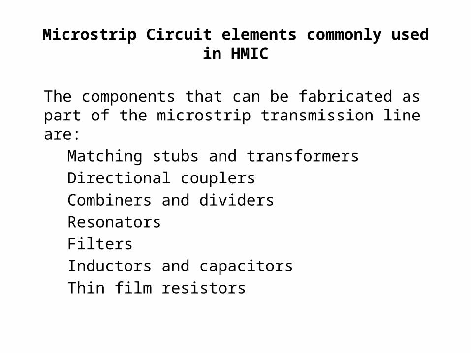
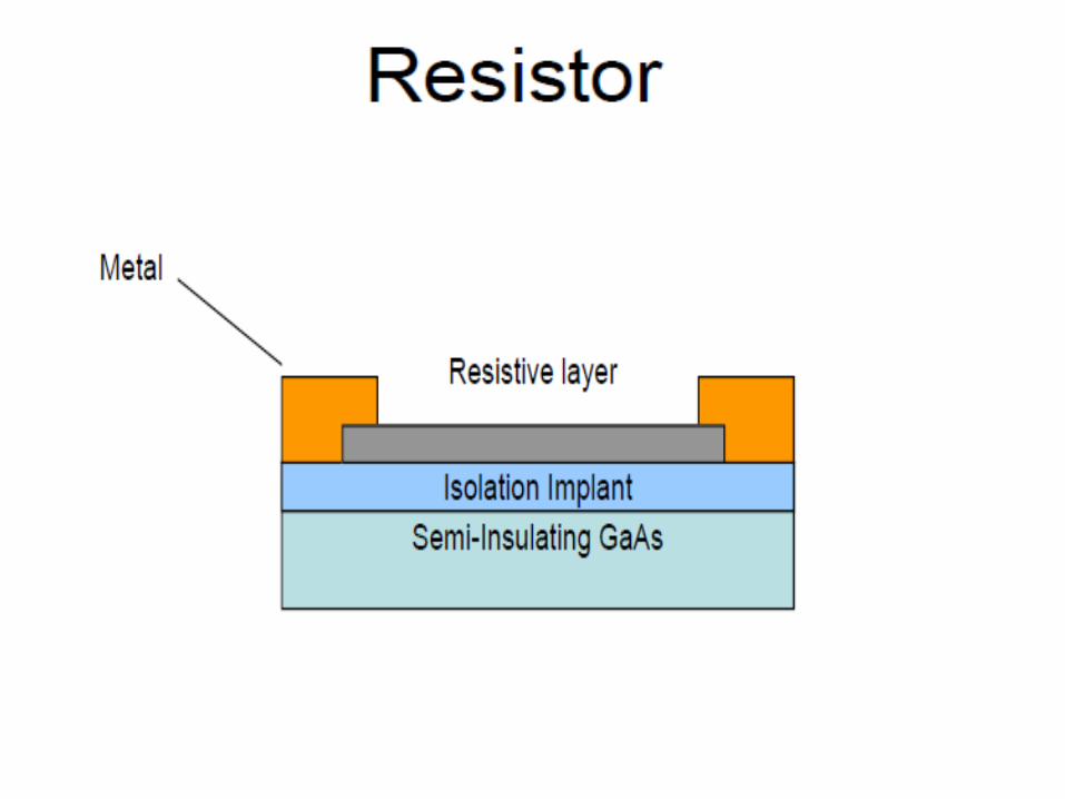
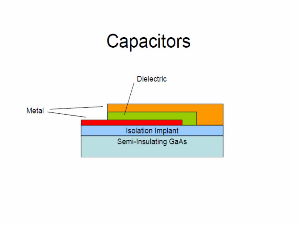
Microstrip Circuit elements commonly used in HMIC
The components that can be fabricated as part of the microstrip transmission line are:
Matching stubs and transformers Directional couplersCombiners and dividersResonatorsFiltersInductors and capacitorsThin film resistors
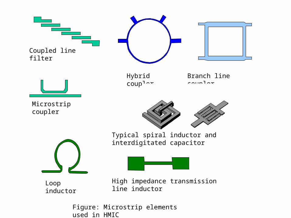
Microstrip coupler
Coupled line filter
Hybrid coupler Branch line coupler
Typical spiral inductor and interdigitated capacitor
Loop inductor High impedance transmission line inductor
Figure: Microstrip elements used in HMIC
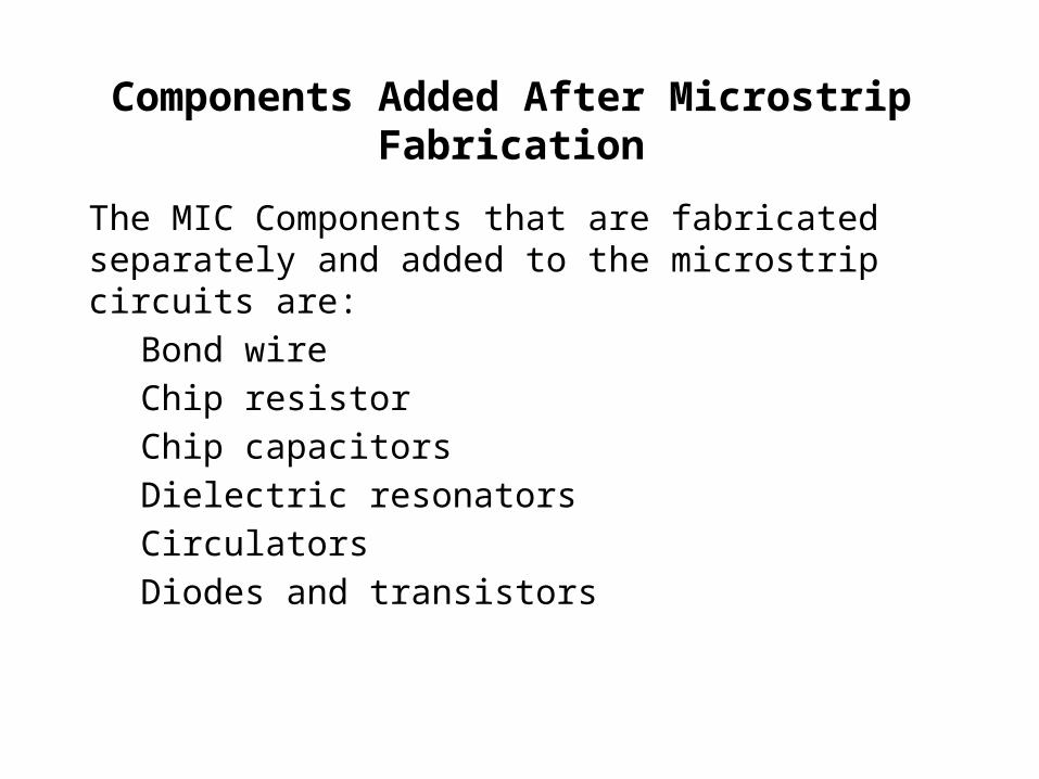
Components Added After Microstrip Fabrication
The MIC Components that are fabricated separately and added to the microstrip circuits are:
Bond wireChip resistorChip capacitorsDielectric resonatorsCirculatorsDiodes and transistors
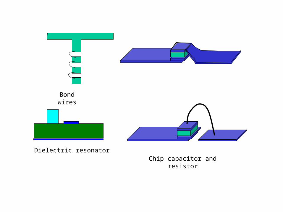
Bond wires
Chip capacitor and resistorDielectric resonator

Microwave Integrated Circuits (MIC)
Microwave circuits exist in three different forms:
Discrete circuitPackaged diodes/transistors mounted in coaxial and waveguide assemblies. Devices can usually be removed from the assembly and replaced
Hybrid MICDiodes/transistors, resonators, capacitors, circulators, … are fabricated separately on most appropriate material and then mounted into the microstrip circuit and connected with bond wires
MMIC Diodes/transistors, resistors, capacitors, microstrip,…all fabricated simultaneously, including their interconnections, in semiconductor chip
Advantages and Disadvantages of HMIC
Advantages:1- Each component can be designed for optimal performance:
Each transistor can be made of the best material. Other devices can be made of the most appropriate material. The lowest loss microwave components can be made by choosing the optimal microstrip substrate.
2- It has high power capability since the high power generating elements can be optimally heat-sinked
3- Standard diodes and transistors can be used and made to perform different functions by using different circuit design.
4- Special-purpose devices for each function are not
required.
5- Trimming adjustments are possible
6- The most economical approach when small quantities, up to several hundred, of the circuits are required.
Disadvantages:1- Wire bonds cause reliability problems. Each circuit
element that is not part of the microstrip assembly must be attached to the microstrip by a wire bond.
2- The number of devices that can be included is limited by the economics of mounting the devices onto the circuit and attaching them by a wire bonds. The circuit is usually limited to a few dozen compartments.
Advantages and Disadvantages of MMICs
Advantages:1- Minimal mismatches and minimal signal delay
2- There are no wire bond reliability problems
3- Up to thousands of devices can be fabricated at one time into a single MMIC.
4- It is the least expensive approach when large quantities are to be fabricated.
Disadvantages:
1- Performance compromised, since the optimal materials cannot be used for each circuit element.
2- Power capability is lower because good heat transfer materials cannot be used
3- Trimming adjustments are difficult or impossible.
4- Unfavorable device-to-chip area ratio in the semiconductor material.
5- Tooling is prohibitively expensive for small quantities of MMIC.
Materials used for MIC
The basic materials for fabricating MICs, in general are divided into four categories:
1- Substrate materials sapphire, alumina, ferrite/garnet, silicon, RT/duroid, quartz, GaAs, Inp, etc.,
2- Conductor materials-copper, gold, silver, aluminum, etc.
3- Dielectric films SiO, SiO2,…etc
4- Resistive films- Nichrome (cNiCr), tantalum (Ta)
Substrate Materials:
1- The cost of the substrate must be justifiable for the application2. Is the technology to be thin- or thick film?3- The choice of thickness and permittivity determines the
achievable impedance range and the usable frequency range.4- There should be low loss tangent for negligible dielectric loss
5- The substrate surface finish should be good (~ 0.1 mm), with relative freedom from voids, to keep conductor loss low and yet maintain good metal-film adhesion
6- There should be good mechanical strength and thermal conductivity.
7- No deformation should be occur during processing of circuit8- A substrates with sufficient size are for the particular
application and complexity should be available
Conductor Materials: High conductivity, low temperature coefficient of resistance, low RF resistance, good adhesion, good etch- ability and solder-ability, and be easy to deposit.
Dielectric Material:Used as insulators for capacitors, protective layer for active devices, and insulating layer for passive circuits.
The desirable properties: Reproducibility, high breakdown voltage, low loss tangent, and the ability to under go processing without developing pin holes
Resistive Films:Required for fabricating resistors for terminations, attenuators, and for bias networks.
The properties required for resistive material are: Good stability, low temperature coefficient of resistivelySheet sensitivities in the range of 10 to 2000 W/square1% accuracy is achievable
The creation of these resistive films demands additional processes of deposition and etching beyond those of the thin-film metallization. This complexity may be obviated by bonding directly chip resistors onto the conducting pattern (ex. using surface mount).