peripheral interfacing 8085 -...
TRANSCRIPT

UNIT - II PERIPHERAL INTERFACING WITH 8085
Peripheral Interfacing is considered to be a main part of Microprocessor, as it is the only way to interact with the external world. The interfacing happens with the ports of the Microprocessor.
• The main IC's which are to be interfaced with 8085 are:
1. 8255 PPI 2. 8259 PIC 3. 8251 USART 4. 8279 Key board display controller 5. 8253 Timer/ Counter 6. A/D and D/A converter interfacing.
PROGRAMMABLE PERIPHERAL INTERFACE - INTEL 8255
Pins, Signals and internal block diagram of 8255:
• It has 40 pins and requires a single +5V supply.
The
INTEL 8255 is a device used to parallel data transfer between processor and slow peripheral devices like ADC, DAC, keyboard, 7-segment display, LCD, etc.
The 8255 has three ports: Port-A, Port-B and Port-C. Port-A can be programmed to work in any one of the three operating modes mode-0, mode-1 and mode-2 as input or output port.
Port-B can be programmed to work either in mode-0 or mode-1 as input or output port.
Port-C (8-pins) has different assignments depending on the mode of port-A and port-B.

If port-A and B are programmed in mode-0, then the port-C can perform any one of the following functions.
As 8-bit parallel port in mode-0 for input or output.. As two numbers of 4-bit parallel ports in mode-0 for input or output. The individual pins of port-C can be set or reset for various control applications. If port-A is programmed in mode- 1/mode-2 and port-B is programmed in mode-1 then some of the pins of port-C are used for handshake signals and the remaining pins can be used as input/ output lines or individually set/reset for control applications.
The read/write control logic requires six control signals. These signals are given below.
1. RD (low):
This control signal enables the read operation. When this signal is low, the microprocessor reads data from a selected I/O port of the 8255A. 2. WR (low):
This control signal enables the write operation. When this signal goes low, the microprocessor writes into a selected I/O port or the control register. 3. RESET:
This is an active high signal. It clears the control register and set all ports in the input mode. 4. CS (low), A0 and A1:
These are device select signals. They are, interfacing of 8255 with 8085 processor:
A simple schematic for interfacing the 8255 with 8085 processor is shown in fig.
PIN DESCRIPTION - INTEL 8255 :
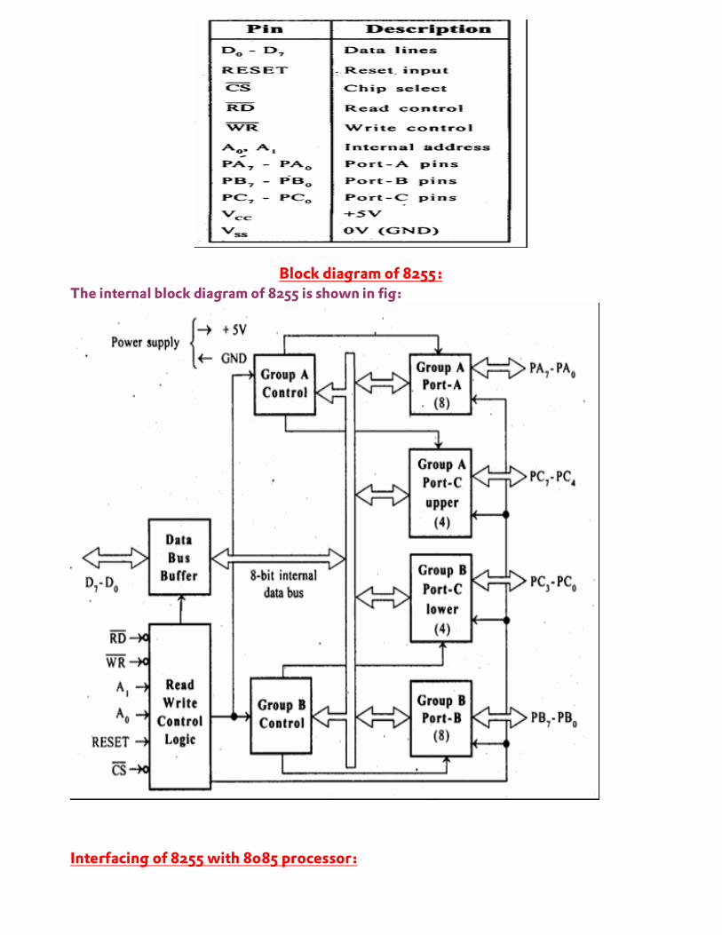
Block diagram of 8255: The internal block diagram of 8255 is shown in fig:
Interfacing of 8255 with 8085 processor:

• A simple schematic for interfacing the 8255 with 8085 processor is
shown in fig.
The 8255 can be either memory mapped or I/O mapped in the system. In the
schematic shown in above is I/O mapped in the system.
• Using a 3-to-8 decoder generates the chip select signals for I/O
mapped devices.
• The address lines A4, A5 and A6 are decoded to generate eight chip
select signals (IOCS-0 to IOCS-7) and in this, the chip select IOCS- 1 is
used to select 8255.
• The address line A7 and the control signal IO/M (low) are used as
enable for the decoder.
• The address line A0 of 8085 is connected to A0 of 8255 and A1 of 8085
is connected to A1 of 8255 to provide the internal addresses.
• The data lines D0-D7 are connected to D0-D7 of the processor to
achieve parallel data transfer.
• The I/O addresses allotted to the internal devices of 8255 are listed in
table.
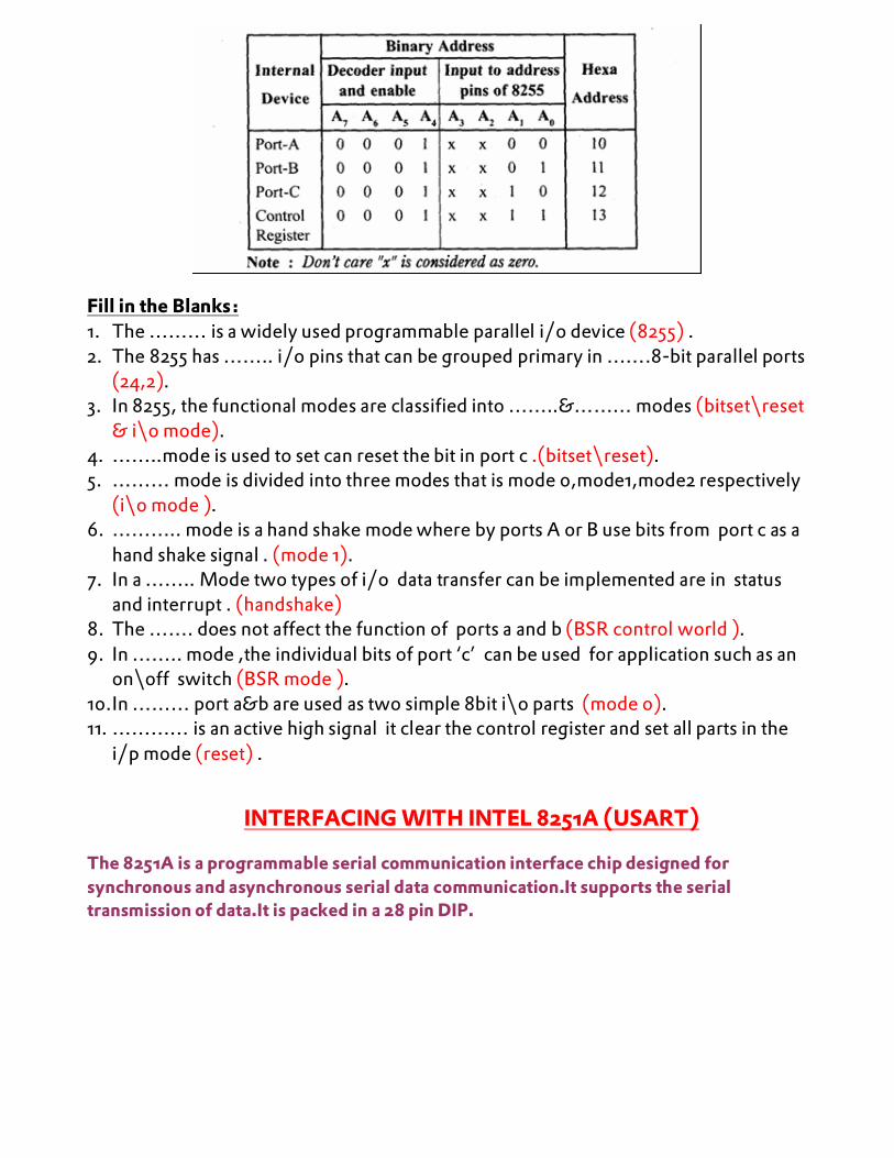
Fill in the Blanks: 1. The ……… is a widely used programmable parallel i/o device (8255) . 2. The 8255 has …….. i/o pins that can be grouped primary in …….8-bit parallel ports
(24,2). 3. In 8255, the functional modes are classified into ……..&……… modes (bitset\reset
& i\o mode). 4. ……..mode is used to set can reset the bit in port c .(bitset\reset). 5. ……… mode is divided into three modes that is mode 0,mode1,mode2 respectively
(i\o mode ). 6. ……….. mode is a hand shake mode where by ports A or B use bits from port c as a
hand shake signal . (mode 1). 7. In a …….. Mode two types of i/o data transfer can be implemented are in status
and interrupt . (handshake) 8. The ……. does not affect the function of ports a and b (BSR control world ). 9. In …….. mode ,the individual bits of port ‘c’ can be used for application such as an
on\off switch (BSR mode ). 10. In ……… port a&b are used as two simple 8bit i\o parts (mode 0). 11. ………… is an active high signal it clear the control register and set all parts in the
i/p mode (reset) .
INTERFACING WITH INTEL 8251A (USART)
The 8251A is a programmable serial communication interface chip designed for synchronous and asynchronous serial data communication.It supports the serial transmission of data.It is packed in a 28 pin DIP.

Block Diagram:
The functional block diagram of 825 1A consists five sections. They are:
• Read/Write control logic • Transmitter • Receiver • Data bus buffer • Modem control.
The functional block diagram is shown in fig:

Read/Write control logic:
The Read/Write Control logic interfaces the 8251A with CPU, determines the functions of the 8251A according to the control word written into its control register. It monitors the data flow.
This section has three registers and they are control register, status register and data buffer.
The active low signals RD, WR, CS and C/D(Low) are used for read/write operations with these three registers.
When C/D(low) is high, the control register is selected for writing control word or reading status word.
When C/D(low) is low, the data buffer is selected for read/write operation.
When the reset is high, it forces 8251A into the idle mode.
The clock input is necessary for 8251A for communication with CPU and this clock does not control either the serial transmission or the reception rate.
Transmitter section:
The transmitter section accepts parallel data from CPU and converts them into serial data.

The transmitter section is double buffered, i.e., it has a buffer register to hold an 8-bit parallel data and another register called output register to convert the parallel data into serial bits.
When output register is empty, the data is transferred from buffer to output register. Now the processor can again load another data in buffer register.
If buffer register is empty, then TxRDY is goes to high.
If output register is empty then TxEMPTY goes to high.
The clock signal, TxC (low) controls the rate at which the bits are transmitted by the USART.
The clock frequency can be 1,16 or 64 times the baud rate.
Receiver Section:
The receiver section accepts serial data and convert them into parallel data
The receiver section is double buffered, i.e., it has an input register to receive serial data and convert to parallel, and a buffer register to hold the parallel data.
When the RxD line goes low, the control logic assumes it as a START bit, waits for half a bit time and samples the line again.
If the line is still low, then the input register accepts the following bits, forms a character and loads it into the buffer register.
The CPU reads the parallel data from the buffer register.
When the input register loads a parallel data to buffer register, the RxRDY line goes high.
The clock signal RxC (low) controls the rate at which bits are received by the USART.
During asynchronous mode, the signal SYNDET/BRKDET will indicate the break in the data transmission.
During synchronous mode, the signal SYNDET/BRKDET will indicate the reception of synchronous character.
MODEM Control:
The MODEM control unit allows to interface a MODEM to 8251A and to establish data communication through MODEM over telephone lines.
This unit takes care of handshake signals for MODEM interface.

The 825 1A can be either memory mapped or I/O mapped in the system.
8251A in I/O mapped in the system is shown in the figure.
Using a 3-to-8 decoder generates the chip select signals for I/O mapped devices.
The address lines A4, A5 and A6 are decoded to generate eight chip select signals (IOCS-0 to IOCS-7) and in this, the chip select signal IOCS-2 is used to select 8251A.
The address line A7 and the control signal IO / M(low) are used as enable for decoder.
The address line A0 of 8085 is connected to C/D(low) of 8251A to provide the internal addresses.
The data lines D0 - D7 are connected to D0 - D7 of the processor to achieve parallel data transfer.
The RESET and clock signals are supplied by the processor. Here the processor clock is directly connected to 8251A. This clock controls the parallel data transfer between the processor and 8251A.
The output clock signal of 8085 is divided by suitable clock dividers like programmable timer 8254 and then used as clock for serial transmission and reception.
The TTL logic levels of the serial data lines and the control signals necessary for serial transmission and reception are converted to RS232 logic levels using MAX232 and then terminated on a standard 9-pin D-.type connector.
In 8251A the transmission and reception baud rates can be different or same.

The device which requires serial communication with processor can be connected to this 9-pin D-type connector using 9-core cable
The signals TxEMPTY, TxRDY and RxRDY can be used as interrupt signals to initiate interrupt driven data transfer scheme between processor and 8251 A.
I/O addresses of 8251A interfaced to 8085 is,
PROGRAMMABLE INTERRUPT CONTROLLER - INTEL 8259
FEATURES OF 8259:
1. It is programmed to work with either 8085 or 8086 processor. 2. It manage 8-interrupts according to the instructions written into its control registers.

3. In 8086 processor, it supplies the type number of the interrupt and the type number is programmable. In 8085 processor, the interrupt vector address is programmable. The priorities of the interrupts are programmable. 4. The interrupts can be masked or unmasked individually. 5. The 8259s can be cascaded to accept a maximum of 64 interrupts.
FUNCTIONAL BLOCK DIAGRAM OF 8259:
It has eight functional blocks. They are,
1. Control logic
2. Read Write logic
3. Data bus buffer
4. Interrupt Request Register (IRR)
5. In-Service Register (ISR)
6. Interrupt Mask Register (IMR)
7. Priority Resolver (PR)
8. Cascade buffer.
The data bus and its buffer are used for the following activities.
1. The processor sends control word to data bus buffer through D0-D7.
2. The processor read status word from data bus buffer through D0-D7
3. From the data bus buffer the 8259 send type number (in case of 8086) or the call opcode and address (in case of 8085) through D0-D7 to the processor.

The processor uses the RD (low), WR (low) and A0 to read or write 8259.
The 8259 is selected by CS (low).
The IRR has eight input lines (IR0-IR7) for interrupts. When these lines go high, the request is stored in IRR. It registers a request only if the interrupt is unmasked.
Normally IR0 has highest priority and IR7 has the lowest priority. The priorities of the interrupt request input are also programmable.
First the 8259 should be programmed by sending Initialization Command Word (ICW) and Operational Command Word (OCW). These command words will inform 8259 about the following,
Type of interrupt signal (Level triggered / Edge triggered).
2. Type of processor (8085/8086).
3. Call address and its interval (4 or 8)
4. Masking of interrupts.
5. Priority of interrupts.
6. Type of end of interrupts.

The interrupt mask register (IMR) stores the masking bits of the interrupt lines to be masked. The relevant information is send by the processor through OCW.
The in-service register keeps track of which interrupt is currently being serviced.
The priority resolver examines the interrupt request, mask and in-service registers and determines whether INT signal should be sent to the processor or not.
The cascade buffer/comparator is used to expand the interrupts of 8259.
In cascade connection one 8259 will be directly interrupting 8086 and it is called master 8259.
To each interrupt request input of master 8259 (IR0-IR7), one slave 8259 can be connected. The 8259s interrupting the master 8259 are called slave 8259s.
Each 8259 has its own addresses so that each 8259 can be programmed independently by sending command words and independently the status bytes can be read from it.
CASCADING 8259: The cascade pins (CAS0, CAS1 and CAS2) from the master are connected to the
corresponding pins of the slave.
For the slave 8259, the SP (low) / EN (low) pin is tied low to let the device know that it is a slave.
The SP (low) / EN (low) pin can be used as input or output signal.
In non-buffered mode it is used as input signal and tied to logic-I in master 8259 and logic-0 in slave 8259.
In buffered mode it is used as output signal to disable the data buffers while data is transferred from 8259A to the CPU.

INTERFACING 8259 WITH 8085 MICROPROCESSOR
It requires two internal address and they are A =0 or A = 1.
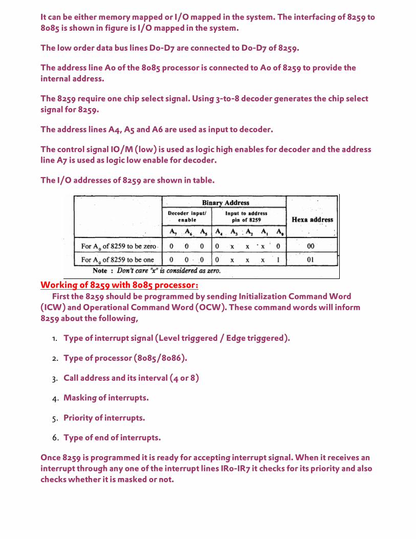
It can be either memory mapped or I/O mapped in the system. The interfacing of 8259 to 8085 is shown in figure is I/O mapped in the system.
The low order data bus lines D0-D7 are connected to D0-D7 of 8259.
The address line A0 of the 8085 processor is connected to A0 of 8259 to provide the internal address.
The 8259 require one chip select signal. Using 3-to-8 decoder generates the chip select signal for 8259.
The address lines A4, A5 and A6 are used as input to decoder.
The control signal IO/M (low) is used as logic high enables for decoder and the address line A7 is used as logic low enable for decoder.
The I/O addresses of 8259 are shown in table.
Working of 8259 with 8085 processor:
First the 8259 should be programmed by sending Initialization Command Word (ICW) and Operational Command Word (OCW). These command words will inform 8259 about the following,
1. Type of interrupt signal (Level triggered / Edge triggered).
2. Type of processor (8085/8086).
3. Call address and its interval (4 or 8)
4. Masking of interrupts.
5. Priority of interrupts.
6. Type of end of interrupts.
Once 8259 is programmed it is ready for accepting interrupt signal. When it receives an interrupt through any one of the interrupt lines IR0-IR7 it checks for its priority and also checks whether it is masked or not.

If the previous interrupt is completed and if the current request has highest priority and unmasked, then it is serviced.
For servicing this interrupt the 8259 will send INT signal to INTR pin of 8085.In response it expects an acknowledge INTA (low) from the processor.
When the processor accepts the interrupt, it sends three INTA (low) one by one.
In response to first, second and third INTA (low) signals, the 8259 will supply CALL opcode, low byte of call address and high byte of call address respectively. Once the processor receives the call opcode and its address, it saves the content of program counter (PC) in stack and load the CALL address in PC and start executing the interrupt service routine stored in this call address.
Fill in the Blanks: 1. The ………. Is a programmable interrupt controller designed to work with micro
processor.(8259) 2. 8259 manage ………….. Interrupts according to the instructions written into its
……….. registers .(8,control) 3. The ………. Logic and A0 determine the port address of the 8259
controller.(chip select) 4. In 8259 the control logic block contains …………. Pin as an o/p and …………
Pin an input.(INT,INTA(low)) 5. The interrupt request register in 8259 ………….. input lines for interrupts.(8) 6. The 8259 requires ………….. and ……………. of control words. (initialization
command words(IEWs) and operational command words.(OEWs)) 7. In a ……………. Mode in which all interrupt requests are arranged from highest
to lowest.(fully nested mode) 8. In mode, a device, after being serviced, receives the lowest priority.(Automatic
rotation mode) 9. In …………. Mode the user can select any IR interrupts request for the lowest
priority, then fixing all other priorities.(Specific rotation mode)
KEYBOARD/DISPLAY CONTROLLER - INTEL 8279
The INTEL 8279 is specially developed for interfacing keyboard and display devices to 8085/8086/8088 microprocessor based system. The important features of 8279 are,
o Simultaneous keyboard and display operations. o Scanned keyboard mode. o Scanned sensor mode. o 8-character keyboard FIFO. o 1 6-character display. o Right or left entry 1 6-byte display RAM. o Programmable scan timing.
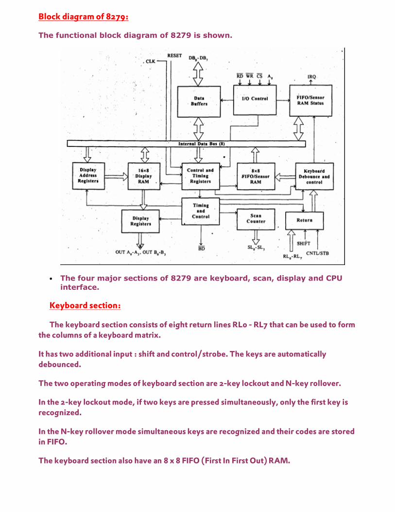
Block diagram of 8279:
The functional block diagram of 8279 is shown.
• The four major sections of 8279 are keyboard, scan, display and CPU
interface.
Keyboard section:
The keyboard section consists of eight return lines RL0 - RL7 that can be used to form the columns of a keyboard matrix.
It has two additional input : shift and control/strobe. The keys are automatically debounced.
The two operating modes of keyboard section are 2-key lockout and N-key rollover.
In the 2-key lockout mode, if two keys are pressed simultaneously, only the first key is recognized.
In the N-key rollover mode simultaneous keys are recognized and their codes are stored in FIFO.
The keyboard section also have an 8 x 8 FIFO (First In First Out) RAM.
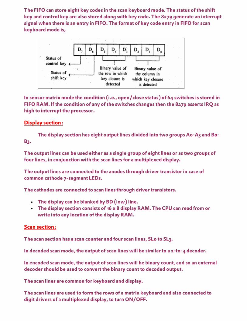
The FIFO can store eight key codes in the scan keyboard mode. The status of the shift key and control key are also stored along with key code. The 8279 generate an interrupt signal when there is an entry in FIFO. The format of key code entry in FIFO for scan keyboard mode is,
In sensor matrix mode the condition (i.e., open/close status) of 64 switches is stored in FIFO RAM. If the condition of any of the switches changes then the 8279 asserts IRQ as high to interrupt the processor.
Display section:
The display section has eight output lines divided into two groups A0-A3 and B0-B3.
The output lines can be used either as a single group of eight lines or as two groups of four lines, in conjunction with the scan lines for a multiplexed display.
The output lines are connected to the anodes through driver transistor in case of common cathode 7-segment LEDs.
The cathodes are connected to scan lines through driver transistors.
• The display can be blanked by BD (low) line. • The display section consists of 16 x 8 display RAM. The CPU can read from or
write into any location of the display RAM.
Scan section:
The scan section has a scan counter and four scan lines, SL0 to SL3.
In decoded scan mode, the output of scan lines will be similar to a 2-to-4 decoder.
In encoded scan mode, the output of scan lines will be binary count, and so an external decoder should be used to convert the binary count to decoded output.
The scan lines are common for keyboard and display.
The scan lines are used to form the rows of a matrix keyboard and also connected to digit drivers of a multiplexed display, to turn ON/OFF.

CPU interface section:
The CPU interface section takes care of data transfer between 8279 and the processor.
This section has eight bidirectional data lines DB0 to DB7 for data transfer between 8279 and CPU.
It requires two internal address A =0 for selecting data buffer and A = 1 for selecting control register of8279.
The control signals WR (low), RD (low), CS (low) and A0 are used for read/write to 8279.
It has an interrupt request line IRQ, for interrupt driven data transfer with processor.
The 8279 require an internal clock frequency of 100 kHz. This can be obtained by dividing the input clock by an internal prescaler.
The RESET signal sets the 8279 in 16-character display with two -key lockout keyboard modes.
Programming the 8279:
The 8279 can be programmed to perform various functions through eight command words.
In a microprocessor b system, when keyboard and 7-segment LED display is interfaced using ports or latches then the processor has to carry the following task.
• Keyboard scanning • Key debouncing • Key code generation • Sending display code to LED • Display refreshing
Interfacing 8279 with 8085 processor:
A typical Hexa keyboard and 7-segment LED display interfacing circuit using 8279 is shown.
The circuit can be used in 8085 microprocessor system and consist of 16 numbers of hexa-keys and 6 numbers of 7-segment LEDs.
The 7-segment LEDs can be used to display six digit alphanumeric character.
The 8279 can be either memory mapped or I/O mapped in the system. In the circuit shown is the 8279 is I/O mapped.
The address line A0 of the system is used as A0 of 8279.
The clock signal for 8279 is obtained by dividing the output clock signal of 8085 by a clock divider circuit.
The chip select signal is obtained from the I/O address decoder of the 8085 system. The chip select signals for I/O mapped devices are generated by using a 3-to-8 decoder.
The address lines A4, A5 and A6 are used as input to decoder.
The address line A7 and the control signal IO/M (low) are used as enable for decoder.
The chip select signal IOCS-3 is used to select 8279.
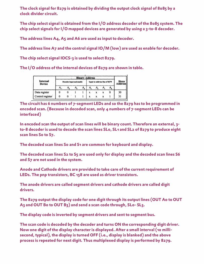
The I/O address of the internal devices of 8279 are shown in table.
The circuit has 6 numbers of 7-segment LEDs and so the 8279 has to be programmed in encoded scan. (Because in decoded scan, only 4 numbers of 7-segment LEDs can be interfaced)
In encoded scan the output of scan lines will be binary count. Therefore an external, 3-to-8 decoder is used to decode the scan lines SL0, SL1 and SL2 of 8279 to produce eight scan lines S0 to S7.
The decoded scan lines S0 and S1 are common for keyboard and display.
The decoded scan lines S2 to S5 are used only for display and the decoded scan lines S6 and S7 are not used in the system.
Anode and Cathode drivers are provided to take care of the current requirement of LEDs. The pnp transistors, BC 158 are used as driver transistors.
The anode drivers are called segment drivers and cathode drivers are called digit drivers.
The 8279 output the display code for one digit through its output lines (OUT A0 to OUT A3 and OUT B0 to OUT B3) and send a scan code through, SL0- SL3.
The display code is inverted by segment drivers and sent to segment bus.
The scan code is decoded by the decoder and turns ON the corresponding digit driver. Now one digit of the display character is displayed. After a small interval (10 milli-second, typical), the display is turned OFF (i.e., display is blanked) and the above process is repeated for next digit. Thus multiplexed display is performed by 8279.

The keyboard matrix is- formed using the return lines, RL0 to RL3 of 8279 as columns and decoded scan lines S0 and S1 as rows.
A hexa key is placed at the crossing point of each row and column. A key press will short the row and column. Normally the column and row line will be high.
During scanning the 8279 will output binary count on SL0 to SL3, which is decoded by decoder to make a row as zero. When a row is zero the 8279 reads the columns. If there is a key press then the corresponding column will be zero.
If 8279 detects a key press then it wait for debounce time and again read the columns to generate key code.
In encoded scan keyboard mode, the 8279 stores an 8-bit code for each valid key press. The keycode consist of the binary value of the column and row in which the key is found and the status of shift and control key.
After a scan time, the next row is made zero and the above process is repeated and so on. Thus 8279 continuously scan the keyboard.
Fill in the Blanks:
1. The 8279 is a hardware approach to introducing a ………&………. (matrix keyboard / multiplexed display).
2. ……… can be connected by contact key matrix (keyboard segment) . 3. keyboard entries are debounced and shared the internal …….. memory (FIFO). 4. ………. Can be provided a 16-character scanned display interface with led’s
(display). 5. The display segment has 16*8……….(R/W RAM). 6. The ……….. consist of eight register that can store eight key board entries (FIFO
RAM). 7. The keyboard can operate in ………&……….. mode (two key lockout , n-key roll
over ). 8. ………… mode if two key are pressed almost simultaneously only the firat key is
recognized (two key lock out ). 9. ……….. mode simultaneously keys are regonized and their codes are shared in
the internal buffer (n key roll over). 10. The scan section of 8279 contains ……..&…….. scan lines (scan counter & 4 ). 11. The display section has ……….. o/p lines divided into two groups .( A0-A3 &B0-
B3 ) 12. The display can be blanked by using the ……. Line (BD) . 13. the mpu interface section include eight ………. and are………and……. lines for
interfacing (8,1,6) . 14. The port address of 8279 register are determined by two signal…….&……….
Programmable Interval Timer 8253/54
Instead of setting up timing loops in system software, the programmer configures the 8253/54 to match his requirements, initializes one of the counters of the 8253/54 with the desired quantity, then upon command the 8253/54 will count out the delay and interrupt the CPU when it has completed its tasks. It is easy to see that the software overhead is minimum and that multiple delays can be easily be maintained by assignment of priority levels. The 8253/54 includes three identical 16 bit counters that can operate independently. To operate a counter, a 16-bit count is loaded in its register and, on command, it begins to decrement the count until it reaches 0. At the end of the count, it generates a pulse that can be used to interrupt the CPU. The counter can count either in binary or BCD.
In addition, a count can be read by the CPU while the counter is decrementing. In this chapter, we are going to study two timer ICs 8253 and 8254. The 8254 is a superset of 8253. The functioning of these two ICs are almost similar along with the pin configuration. Only the differences are :
Features 1) Three independent 16-bit down counters. 2) 8254 can handle inputs from DC to 10 MHz (5MHz 8254-5 8MHz 8254 10MHz 8254-2) where as 8253 can operate upto 2.6 MHz. 3) Three counters are identical presettable, and can be programmed for either binary or BCD count. 4) Counter can be programmed in six different modes. 5) Compatible with all Intel and most other microprocessors. 6) 8254 has powerful command called READ BACK command which allows the user to check the count value, programmed mode and current mode and current status of the counter.
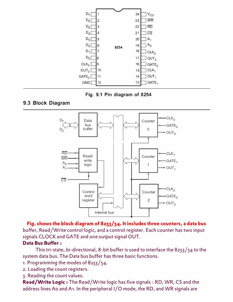
Fig. shows the block diagram of 8253/54. It includes three counters, a data bus
buffer, Read/Write control logic, and a control register. Each counter has two input signals CLOCK and GATE and one output signal OUT. Data Bus Buffer :
This tri-state, bi-directional, 8-bit buffer is used to interface the 8253/54 to the system data bus. The Data bus buffer has three basic functions. 1. Programming the modes of 8253/54. 2. Loading the count registers. 3. Reading the count values. Read/Write Logic : The Read/Write logic has five signals : RD, WR, CS and the address lines A0 and A1. In the peripheral I/O mode, the RD, and WR signals are
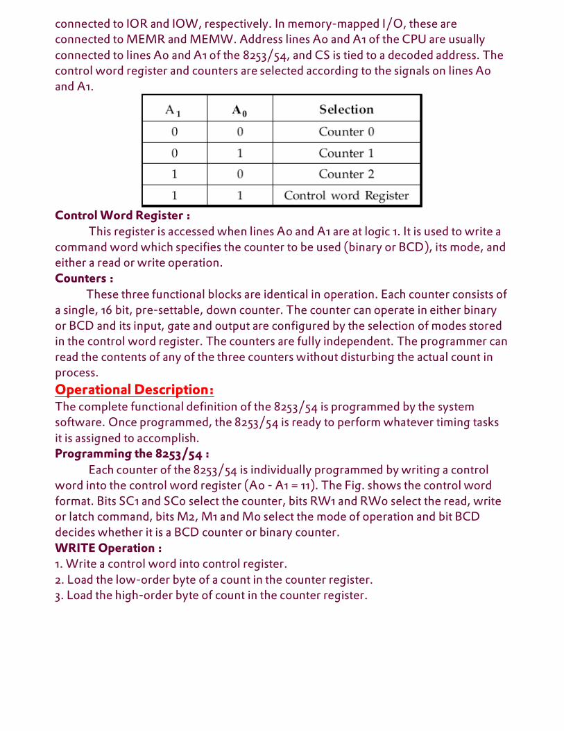
connected to IOR and IOW, respectively. In memory-mapped I/O, these are connected to MEMR and MEMW. Address lines A0 and A1 of the CPU are usually connected to lines A0 and A1 of the 8253/54, and CS is tied to a decoded address. The control word register and counters are selected according to the signals on lines A0 and A1.
Control Word Register :
This register is accessed when lines A0 and A1 are at logic 1. It is used to write a command word which specifies the counter to be used (binary or BCD), its mode, and either a read or write operation. Counters :
These three functional blocks are identical in operation. Each counter consists of a single, 16 bit, pre-settable, down counter. The counter can operate in either binary or BCD and its input, gate and output are configured by the selection of modes stored in the control word register. The counters are fully independent. The programmer can read the contents of any of the three counters without disturbing the actual count in process.
Operational Description: The complete functional definition of the 8253/54 is programmed by the system software. Once programmed, the 8253/54 is ready to perform whatever timing tasks it is assigned to accomplish. Programming the 8253/54 :
Each counter of the 8253/54 is individually programmed by writing a control word into the control word register (A0 - A1 = 11). The Fig. shows the control word format. Bits SC1 and SC0 select the counter, bits RW1 and RW0 select the read, write or latch command, bits M2, M1 and M0 select the mode of operation and bit BCD decides whether it is a BCD counter or binary counter. WRITE Operation : 1. Write a control word into control register. 2. Load the low-order byte of a count in the counter register. 3. Load the high-order byte of count in the counter register.
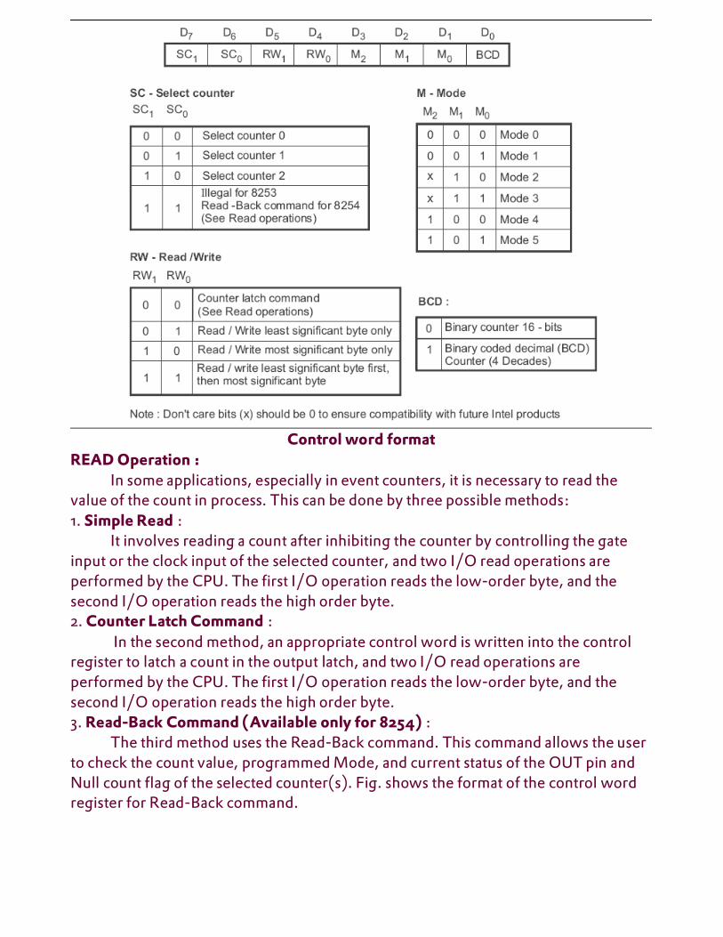
Control word format
READ Operation : In some applications, especially in event counters, it is necessary to read the
value of the count in process. This can be done by three possible methods: 1. Simple Read :
It involves reading a count after inhibiting the counter by controlling the gate input or the clock input of the selected counter, and two I/O read operations are performed by the CPU. The first I/O operation reads the low-order byte, and the second I/O operation reads the high order byte. 2. Counter Latch Command :
In the second method, an appropriate control word is written into the control register to latch a count in the output latch, and two I/O read operations are performed by the CPU. The first I/O operation reads the low-order byte, and the second I/O operation reads the high order byte. 3. Read-Back Command (Available only for 8254) :
The third method uses the Read-Back command. This command allows the user to check the count value, programmed Mode, and current status of the OUT pin and Null count flag of the selected counter(s). Fig. shows the format of the control word register for Read-Back command.

Control word register for read-back command
The Read-Back command may be used to latch multiple counter output latches by setting the COUNT bit D5 = 0 and selecting the desired counter (s). Each counter’s latch count in held until it is read (or the counter is reprogrammed). That counter is automatically unlatched when read. Other Features of Read - Back Command (Available only for 8254) :
The Read-Back command may also be used to latch status information of selected counter(s) by setting STATUS bit D4 = 0. The contents of the counter must be latched before reading. The status of a counter is then accessed by a read from that counter. The Fig. shows the counter status format.
Bit D5 - D0 contains the counter’s programmed mode exactly as written in the last mode control word. Bit D7 contains the current status of the output pin. In 8254, it is not possible to read count from the counter, if the count is not loaded into the counting element (CE). The Bit D6 indicates whether the counting element has count or not. If D6 = 0, counting element has count otherwise null count. Interleaved Read and Write :
Another feature of the 8254 is that reads and writes of the same counter may be interleaved. For example, if the counter is programmed for the two byte counts, the following sequence is valid. 1. Read least significant byte. 2. Write new least significant byte. 3. Read most significant byte. 4. Write new most significant byte
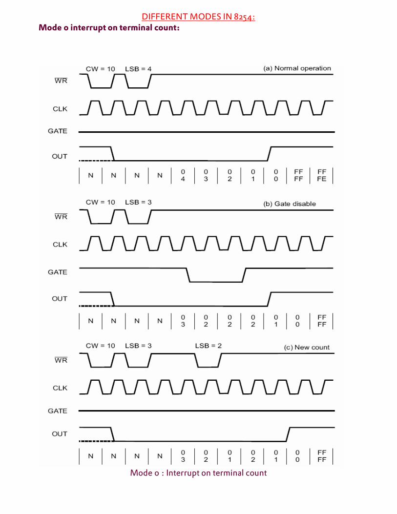
DIFFERENT MODES IN 8254: Mode 0 interrupt on terminal count:
Mode 0 : Interrupt on terminal count

a) Normal Operation : 1) The output will be initially low after the mode set operation. 2) After the count is loaded into the selected count Register the output will remain low and the counter will count. 3) When the terminal count is reached the output will go high and remain high until the selected count is reloaded. b) Gate Disable 1) Gate = 1 enables counting. 2) Gate = 0 disables counting. Note : Gate has no effect on OUT. c) New Count If a new count is written to the counter, it will be loaded on the next CLK pulse and counting will continue from the new count In case of two byte count : 1) Writing the first byte disables counting. 2) Writing the second byte loads the new count on the next CLK pulse and counting will continue from the new count. MODE 1 : Hardware Retriggerable One-shot:

a) Normal operation 1) The output will be initially high 2) The output will go low on the CLK pulse following the rising edge at the gate input. 3) The output will go high on the terminal count and remain high until the next rising edge at the gate input. b) Retriggering The one shot is retriggerable, hence the output will remain low for the full count after any rising edge of the gate input. c) New count If the counter is loaded during one shot pulse, the current one shot is not affected unless the counter is retriggered. If retriggered, the counter is loaded with the new count and the one-shot pulse continues until the new count expires. MODE 2 : Rate generator This mode functions like a divide by-N counter. a) Normal Operation 1) The output will be initially high. 2) The output will go low for one clock pulse before the terminal count. 3) The output then goes high, the counter reloads the initial count and the process is repeated. 4) The period from one output pulse to the next equals the number of input counts in the count register. b) Gate Disable 1) If Gate = 1 it enables a counting otherwise it disables counting (Gate = 0 ). 2) If Gate goes low during an low output pulse, output is set immediately high. A trigger reloads the count and the normal sequence is repeated. c) New count :
The current counting sequence does not affect when the new count is written. If a trigger is received after writing a new count but before the end of the current period, the new count will be loaded with the new count on the next CLK pulse and counting will continue from the new count. Otherwise, the new count will be loaded at the end of the current counting cycle. Note : In mode 2, a count of 1 is illegal.
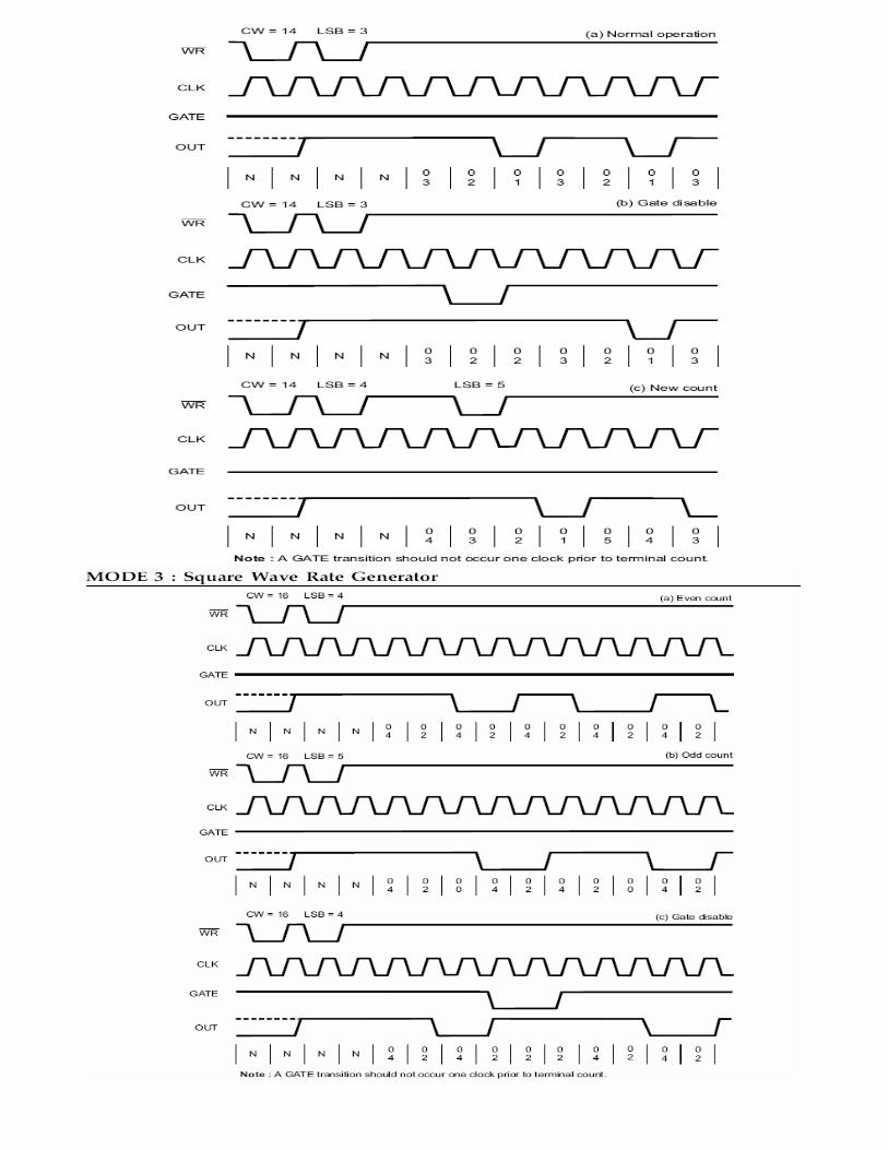
a) Normal operation 1) Initially output is high. 2) For even count, counter is decremented by 2 on the falling edge of each clock pulse. When the counter reaches terminal count, the state of the output is changed and the counter is reloaded with the full count and the whole process is repeated. 3) If the count is odd and the output is high the first clock pulse (after the count is loaded) decrements the count by 1. Subsequent clock pulses decrement the clock by 2. After timeout, the output goes low and the full count is reloaded. The first clock pulse (following the reload) decrements the count by 3 and subsequent clock pulse decrement the count by two. Then the whole process is repeated. In this way, if the count is odd, the output will be high for (n+1)/2 counts and low for (n-1)/2 counts. b) Gate Disable
If Gate is 1 counting is enabled otherwise it is disabled. If Gate goes low while output is low, output is set high immediately. After this, When Gate goes high, the counter is loaded with the initial count on the next clock pulse and the sequence is repeated. c) New Count
The current counting sequence does not affect when the new count is written. If a trigger is received after writing a new count but before the end of the current half-cycle of the square wave, the counter will be loaded with the new count on the next CLK pulse and counting will continue from the new count. otherwise, the new count will be loaded at end of the current half-cycle. MODE 4 : Software Triggered Strobe. a) Normal operation 1) The output will be initially high 2) The output will go low for one CLK pulse after the terminal count (TC). b) Gate Disable If Gate is one the counting is enabled otherwise it is disabled. The Gate has no effect on the output. c) New count If a new count is written during counting, it will be loaded on the next CLK pulse and counting will continue from the new count. If the count is two byte then 1) Writing the first byte has no effect on counting. 2) Writing the second byte allows the new count to be loaded on the next CLK pulse. MODE 5 : Hardware triggered strobe (Retriggerable). a) Normal operation 1) The output will be initially high. 2) The counting is triggered by the rising edge of the Gate. 3) The output will go low for one CLK pulse after the terminal count (TC). b) Retriggering

If the triggering occurs on the Gate input during the counting, the initial count is loaded on the next CLK pulse and the counting will be continued until the terminal count is reached. c) New count
If a new count is written during counting, the current counting sequence will not be affected. If the trigger occurs after the new count is written but before the terminal count, the counter will be loaded with the new count on the next CLK pulse and counting will continue from there. Table 9.1 shows the gate pin operations.
Example 1: Write a program to initialize counter 2 in mode 0 with a count of C030H.
Assume address for control register = 0BH, counter 0 = 08H, counter 1 = 09H
and counter 2 = 0AH.
Sol. : Control word
Source Program MOV AL,B0H OUT 0BH,AL ; Loads control word (B0H) in the control ; register. MOV AL,30H OUT 0AH,AL ; Loads lower byte of (30H)the count. MOV AL,0C0H OUT 0AH,AL ; Loads higher byte (C0H) of the count