performances of spin coated silver doped zno … 37 07.pdfperformances of spin coated silver doped...
TRANSCRIPT
Processing and Application of Ceramics 11 [3] (2017) 213–219
https://doi.org/10.2298/PAC1703213S
Performances of spin coated silver doped ZnO photoanode based dye
sensitized solar cell
Amrik Singh1,∗, Devendra Mohan2, Dharamvir Singh Ahlawat1, Richa3
1Material Science Lab., Department of Physics, Chaudhary Devi Lal University, Sirsa-125055 Haryana, India2Laser Laboratory, Department of Applied Physics, Guru Jambheshwar University of Science & Technology,
Hisar-125001, Haryana, India3Research Scholar, Department of Physics, I.K. Gujral Punjab Technical University, Kapurthala-144601,
Punjab, India
Received 12 March 2017; Received in revised form 23 July 2017; Received in revised form 8 September 2017;Accepted 16 September 2017
Abstract
Dye sensitized solar cells (DSSCs) were fabricated using silver doped ZnO films deposited on ITO glass byspin coating method. The crystalline nature of ZnO films was analysed with XRD and SEM technique wasused for morphological studies. The XRD pattern confirmed the presence of single phase hexagonal wurtziteZnO structure, without the presence of secondary phase. The crystallite size of ZnO decreased from 31 nm to25 nm with increase in doping to 1.5 mol% of silver. The UV-visible transmission of the prepared ZnO filmwas found to be 70–90% and it decreased with increase in doping to 0.5 mol% Ag and increased in the filmdoped with 1.5 mol% Ag. The band gap values of the ZnO films with 0, 0.5 and 1.5 mol% of silver, determinedfrom Tauc plot, were 3.269, 3.235 and 3.257 eV, respectively. The absorbance peaks of the N719 dye loadedZnO films were obtained at the wavelengths 310, 350 and 538 nm. The N719 dye loaded ZnO film doped with0.5 mol% Ag has the highest absorbance in the visible region as compared to other two samples. The fill factorvalues of the pure and ZnO doped with 0.5 and 1.5 mol% Ag were 0.47, 0.48 and 0.42, respectively. The shortcircuit density values for ZnO, ZnO:Ag0.5% and ZnO:Ag1.5% were found to be 1.50, 1.55 and 1.15 A·m/cm2,respectively. The calculated photon to electron efficiencies for the ZnO films with 0, 0.5 and 1.5 mol% of silverwere 0.42%, 0.44% and 0.27%, respectively. Consequently future prospective of such type of dopants in ZnOfilm based dye sensitized solar cells seems to be bright.
Keywords: Ag doped ZnO films, spin coating technique, solar cell, band gap, photovoltaic performances
I. Introduction
Dye sensitized solar cells (DSSCs) have attractedconsiderable attention due to their low cost and rela-tively high photovoltaic performance [1–3].The DSSCsconsist of photoanode, counterelectrode and elec-trolytes. The photoelectrode have semiconductor ox-ide layer like ZnO, TiO2 and dye adsorbed into semi-conductor oxide layer. On the other side, platinum orgraphite acts as counterelectrode and iodine as redoxcouple electrolyte [4–8]. Transparent conducting oxidecoated glass like ITO has been the main choice for thesubstrate material for the DSSC, due to its excellent op-
∗Corresponding author: tel: +919017447500,e-mail: [email protected]
tical, electrical and encapsulation barrier properties. Asincident photons are absorbed by dye molecules, elec-trons are being injected from their excited states intothe conduction band of the TiO2/ZnO nanoparticles andthe dye molecule gets oxidized. Oxidized dye moleculesare reduced by a redox electrolyte, which transports thepositive charges by diffusion to a counterelectrode [9–13]. Efficient electron injection from excited state of thedye to TiO2 plays an important role in DSSC [14–17].Zinc oxide materials have drawn the attention of re-searchers because of the wide band gap and its applica-tions in electronics, photoelectronics and sensors [18].The ZnO material possesses a wide band gap, low resis-tance and high light trapping characteristics that makeit suitable for solar cells applications. The pure ZnO
213
A. Singh et al. / Processing and Application of Ceramics 11 [3] (2017) 213–219
nanostructures show weak optical features that are resultof point defects such as oxygen vacancies or interstitialZn. Therefore, they cannot be used directly in the indus-try [19]. As a result, doping of ZnO with a convenient el-ement can be used to modify optical and magnetic prop-erties. Furthermore, in order to make optoelectronic de-vices, n-type and p-type states are needed [20–22]. Themost commonly occurring lanthanide/transition metalsare used as dopants. This is because these compoundshave been widely used as high-performance lumines-cent devices, magnets, catalysts, and other functionalmaterials. Many researchers have reported the influ-ence of annealing temperature of doped ZnO film onthe DSSCs performances [23]. Efficiency of the cell canalso be improved by modifying the various parameterslike thickness, porosity of semiconductor oxide pho-toanode and counterelectrode of DSSCs [24–26]. Sahu[27] reported the influences of dopant concentration andsubstrate temperature on the properties of the Ag-ZnOfilms. Duan et al. [28,29] reported the synthesis of Ag-ZnO films on Si substrates by DC reactive sputteringtechnique. The Ag doped ZnO films exhibit various op-tical and electrical properties that depend on the deposi-tion temperature and silver content.
ZnO thin films can be synthesized by using differentfabrication methods, including vapour phase process-ing approaches such as physical vapour deposition andchemical vapour deposition and wet solution process-ing approaches such as sol-gel process [30,31]. Differ-ent techniques result in different properties of ZnO thinfilms [32,33]. The sol-gel spin coating method has beenwidely adopted for the fabrication of transparent andconducting oxide due to its simplicity, safety, no needof costly vacuum system and applicability for large areacoating. The sol-gel method also offers other advantagessuch as suitable surface morphology at low crystallizingtemperature and the easy control of chemical compo-nents during sol-gel preparation [33,34]. Proper selec-tion of concentration and nature of dopants in host mate-rials like ZnO may improve the photon to electron con-version efficiency of DSSCs. Different types of dopantsoffer much broader range of possibilities that favour theperformance of DSSCs. For a case, doping of such typeof materials in ZnO photoanode may have possibilityto open new avenues for unique optical, structural andelectrical properties that could be helpful in researchand industry related to renewable energy sources withbroad application perspectives.
In the present work, silver doped ZnO thin films weredeposited on ITO glass by sol-gel spin coating. Theaim of this work was to produce p-type doping of ZnOfilm/ITO substrate to be used in practical applications.The deposited ZnO films on ITO substrate act as pho-toanodes for dye sensitized solar cells. Structure and op-tical properties have also been investigated for ZnO thinfilm samples. The photovoltaic performance of assem-bled solar cells was analysed.
II. Experimental
2.1. ZnO and Ag doped ZnO sol preparation
Zinc acetate dehydrate (Sigma Aldrich) and silvernitrate (Sigma Aldrich, 99.9%) were taken as ZnOand silver precursors, respectively. Firstly 5.949 g ofzinc acetate dehydrate was added into 25 ml of ethanoland stirred for one hour at 60 °C and then mono-ethanolamine (Merck, 99% USA) was added into it. Aclear and transparent ZnO sol was obtained after some-time and left at room temperature for 24 hours. Molarratio of zinc acetate dihydrate and ethanolamine wasmaintained at 1 : 1 [33]. In addition to the pure ZnO, twodoped ZnO sols with 0.5 and 1.5 mol% of silver wereprepared by dissolving of appropriate amount of silvernitrate into acetonitrile (Sigma Aldrich 99.9%) and thenadded into stirred ZnO sol.
2.2. Photoanode preparation
Photoelectrode of ZnO and doped ZnO films wereprepared by deposition of the obtained sols on ITO sub-strate via spin coating technique and scotch tape wasused as a spacer. The speed of spin coater (MTI Cor-poration) was adjusted at 3000 rpm during one minuteand then each film was dried on hot plate maintainedat 180 °C for 10 minutes for removal of extra solvents.For desired thickness of films the steps of coating wereperformed three times and then the films were annealedat 550 °C for 1 h, with ramp rate of 10 °C/min. Thethicknesses of films were obtained in the range of 310–330 nm.
For sensitization purposes, the as-fabricated photo-electrodes were dipped in dye solution (mixture of0.5 mM of N719 dye and ethanol) for 24 hours andwashed with ethanol for the removal of extra dye andthen dried.
2.3. Counterlectrode preparation
For the preparation of platinum coated ITO/glasscounterelectrode, the solution was made from 5 mMPtCl4 (Sigma Aldrich, 99.9%) in isopropanol. The so-lution was poured on ITO glass substrate and spun for1 min at 2800 rpm. The platinum films were dried at130 °C for 15 minutes on the hot plate and then sin-tered at 400 °C for 15 minutes for removal of extra sol-vents [22]. Finally, the light grey coloured films wereobtained.
2.4. Assembling of DSSCs
For the complete fabrication of DSSCs the dye sen-sitized photoelectrode and counterlectrode were com-bined together and an electrolyte solution was injectedbetween the electrodes. Electrolyte solution (browncoloured) was made from 0.05 M lithium iodide (LiISigma Aldrich, 99.9%) and 0.5 mM iodine (I2, SigmaAldrich, 99.9%) in acetonitrile (Sigma Aldrich 99.9%)[22].
214
A. Singh et al. / Processing and Application of Ceramics 11 [3] (2017) 213–219
2.5. Characterization techniques
The XRD patterns of the prepared films were ob-tained by Rigaku Miniflex 600 diffractometer (usingCu-Kα, scan speed of 0.5–2°/min and λ = 1.541 Å).The crystallite size D was calculated using Scherrer for-mula [35]:
D =k · λ
β cos θ(1)
where β is the full width at half maximum of thediffraction 101 peak, λ is the X-ray wavelength andθ is the Bragg’s angle. The SEM images of the sam-ples were studied by JEOL scanning electron micro-scope (SEM JEOL) and UV-visible transmission spectrawere recorded by UV-visible spectrometer set up (SHI-MAZDU, UV 200–1000 nm). The photocurrent-voltage(J-V) characteristics of the assembled devices weremeasured using using AM-1.5 solar simulator (NewPort Model, 96000) with xenon lamp (max. 150 W) andsource meter (Keithley, Model 2400) at room tempera-ture. Incident light intensity and active cell area were100 mW/cm2 (one sun illumination) and 1×1 cm, re-spectively. The thickness of the thin films was measuredby Ellipsometer set up (Model No: HO-ED-P15, rota-tion range 70 degrees).
III. Results and discussion
3.1. Structural characterization
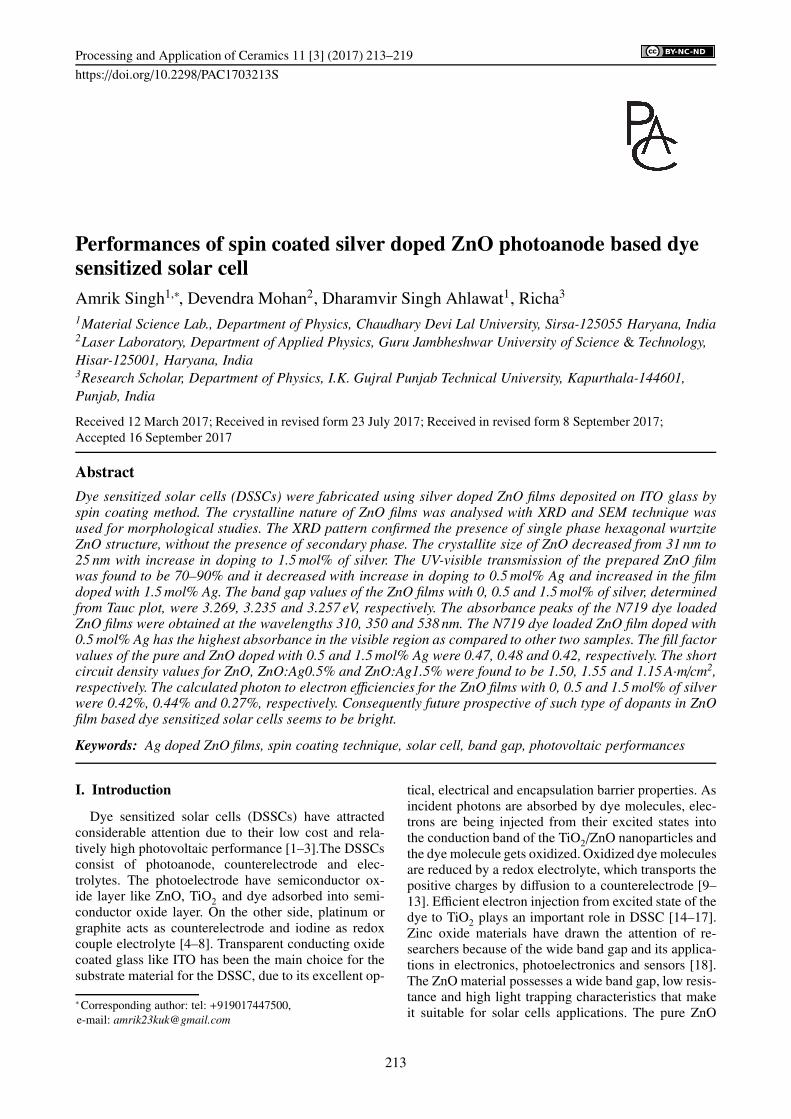
The crystallinity, crystallographic orientation andphase evaluation of the sol-gel spin coated ZnO filmswere examined by XRD measurements, as presented inFig. 1. The XRD pattern confirms that ZnO has hexag-onal wurtzite structure [28,29]. The main peaks of ZnOfilm correspond to the crystalline planes (100), (002),(101), (102) and (110) at angles of 32.68°, 35.34°,36.68°, 48.16° and 57.32°, respectively. With 0.5 mol%doping of silver the peak corresponding to (101) plane
shifted slightly to lower angle and again shifted tohigher angle side at 1.5 mol% doping, which meansthat stress or strain were produced in the film. Theintensity of XRD peak corresponding to plane (101)slightly degraded for the sample with 1.5 mol% of silver.From XRD analysis, the crystallite size correspondingto (101) plane of the pure and doped ZnO with 0.5 and1.5 mol% silver were around 31, 30 and 25 nm, respec-tively. The slight degradation in peaks intensity foundin the sample with 1.5 mol% of Ag is most likely due tothe distortion in crystalline structure [36,37]. Structuralparameters of the films are presented in Table 1.
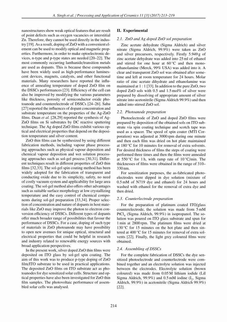
Figures 2a, 2b and 2c show the SEM images of ZnO,ZnO:Ag0.5% and ZnO:Ag1.5%, respectively. The SEMimage of the pure ZnO film shows that there is a uniformarrangement of grains. The average grain size of ZnOwas measured as 44.5 nm. The surface of the ZnO filmdoped with 1.5 mol% Ag seems to be smooth, comparedto other samples.
Figure 1. XRD pattern of silver doped ZnO films
Table 1. Structural parameters of ZnO films
Sample FWHM [°] Peak position [°] Crystallite size [nm]ZnO 0.2824 36.68 30.97
ZnO:Ag0.5% 0.2902 36.58 30.13ZnO:Ag1.5% 0.3512 37.0 24.91
(a) (b) (c)
Figure 2. SEM images of a) pure ZnO film, b) ZnO:Ag0.5% and c) ZnO:Ag1.5%
215
A. Singh et al. / Processing and Application of Ceramics 11 [3] (2017) 213–219
3.2. Optical properties
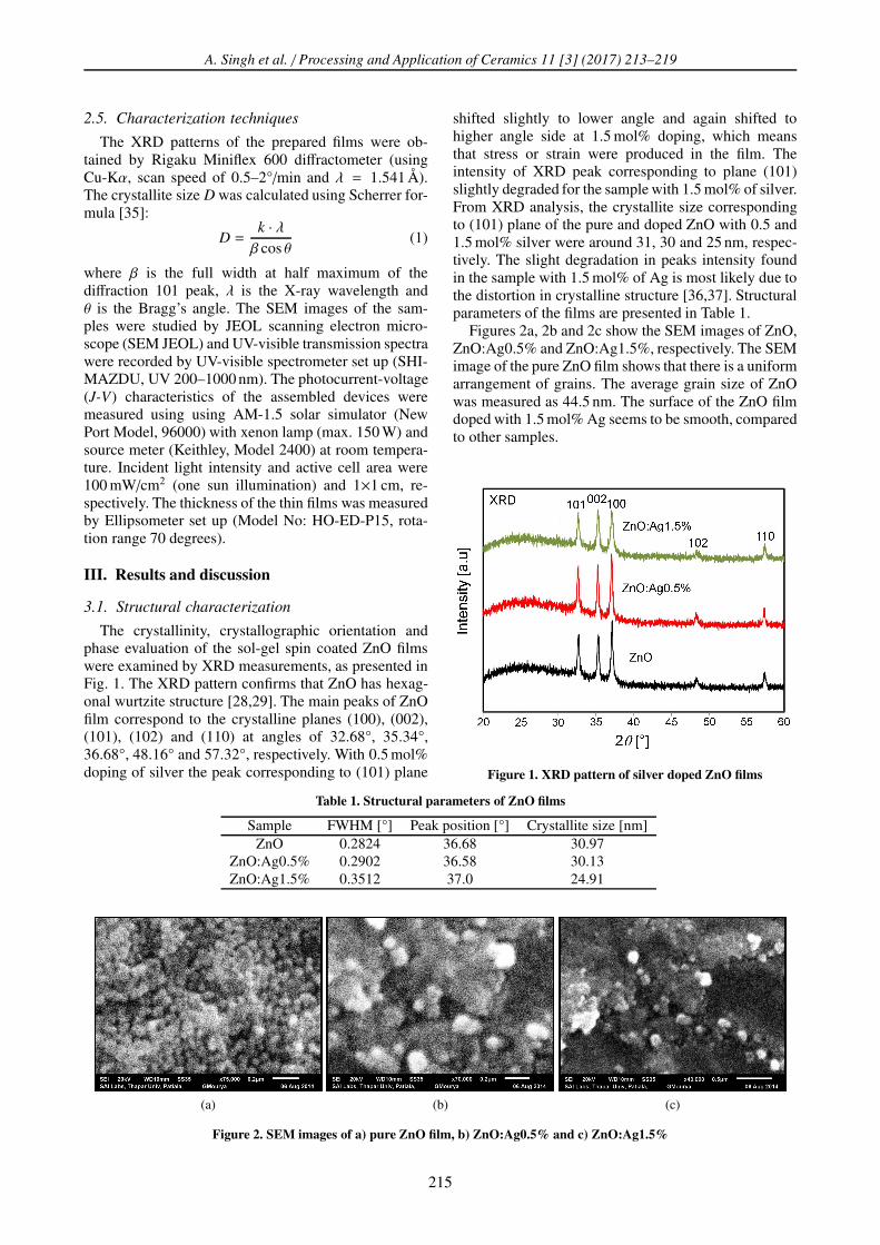
Investigation of optical properties of the sol-gel spincoated ZnO thin films has been performed by UV-visible spectroscopy and the results are shown in Figs.3 and 4. The absorbance of ZnO films is in the rangeof 6–30% in the visible portion of spectrum. The ab-sorbance of the ZnO films slightly increases with addi-tion of 0.5 mol% Ag and decreases with higher amountof silver (1.5 mol% Ag).
The transmission of the ZnO films was in the rangeof 65–90% in the portion of visible spectrum. With theincrease in doping to 0.5 mol% of silver the transmis-sion of the film slightly decreases and then it increasesfor the ZnO film with 1.5 mol% of silver. The slight de-crease in transmittance was due to rough and poroussurface of the film, while smooth surface of 1.5 mol%ZnO has increased the transmittance. Sutanto et al. havealso reported similar types of results in the case of ZnOfilms [38]. Kim et al. also reported the behaviour of ab-sorbance for doped ZnO films [39].
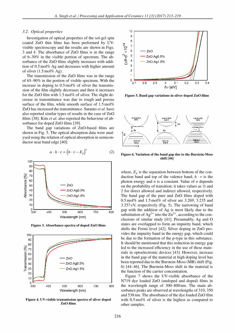
The band gap variations of ZnO-based films areshown in Fig. 5. The optical absorption data were anal-ysed using the relation of optical absorption in semicon-ductor near band edge [40]:
α · h · ν =(
h · ν − Eg
)n(2)
Figure 3. Absorbance spectra of doped ZnO films
Figure 4. UV-visible transmission spectra of silver dopedZnO films
Figure 5. Band gap variations in silver doped ZnO films
Figure 6. Variation of the band gap due to the Burstein-Mossshift [44]
where, Eg is the separation between bottom of the con-duction band and top of the valence band, h · ν is thephoton energy and n is a constant. Value of n dependson the probability of transition; it takes values as 1/2 and2 for direct allowed and indirect allowed, respectively.The band gap of the pure and ZnO films doped with0.5 mol% and 1.5 mol% of silver are 3.269, 3.235 and3.257 eV, respectively (Fig. 5). The narrowing of bandgap with the addition of Ag is most likely due to thesubstitution of Ag2+ into the Zn2+, according to the con-clusions of similar study [41]. Presumably, Ag and Ostates are overlapped to form an impurity band, whichshifts the Fermi level [42]. Silver doping in ZnO pro-vides the impurity band in the energy gap, which couldbe due to the formation of the p-type in this substance.It should be mentioned that this reduction in energy gapled to the increased efficiency in the use of these mate-rials in optoelectronic devices [43]. However, increasein the band gap of the material at high doping level hasbeen reported due to the Burstein-Moss (MB) shift (Fig.6) [44–46]. The Burstein-Moss shift in the material isthe function of the carrier concentration.
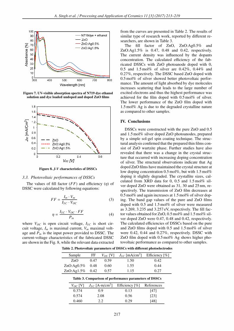
Figure 7 shows the UV-visible absorbance of theN719 dye loaded ZnO (undoped and doped) films inthe wavelength range of 300–800 nm. The main ab-sorbance peaks are observed at wavelengths of 310, 350and 538 nm. The absorbance of the dye loaded ZnO filmwith 0.5 mol% of silver is the highest as compared toother samples.
216
A. Singh et al. / Processing and Application of Ceramics 11 [3] (2017) 213–219
Figure 7. UV-visible absorption spectra of N719 dye ethanolsolution and dye loaded undoped and doped ZnO films
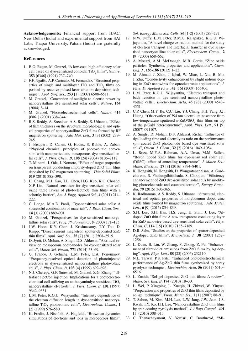
Figure 8. J-V characteristics of DSSCs
3.3. Photovoltaic performances of DSSCs
The values of fill factor (FF) and efficiency (η) ofDSSC were calculated by following equations:
FF =Im · Vm
ISC · VOC
(3)
η =ISC · VOC · FF
Pin
(4)
where VOC is open circuit voltage, ISC is short cir-cuit voltage, Im is maximal current, Vm maximal volt-age and Pin is the input power provided to DSSC. Thecurrent-voltage characteristics of the fabricated DSSCare shown in the Fig. 8, while the relevant data extracted
from the curves are presented in Table 2. The results ofsimilar type of research work, reported by different re-searchers, are shown in Table 3.
The fill factor of ZnO, ZnO:Ag0.5% andZnO:Ag1.5% is 0.47, 0.48 and 0.42, respectively.The current density was influenced by the dopantsconcentration. The calculated efficiency of the fab-ricated DSSCs with ZnO photoanode doped with 0,0.5 and 1.5 mol% of silver are 0.42%, 0.44% and0.27%, respectively. The DSSC based ZnO doped with0.5 mol% of silver showed better photovoltaic perfor-mance. The amount of light absorbed by dye moleculesincreases scattering that leads to the large number ofexcited electrons and thus the highest performance wasachieved for the film doped with 0.5 mol% of silver.The lower performance of the ZnO film doped with1.5 mol% Ag is due to the degraded crystalline natureas compared to other samples.
IV. Conclusions
DSSCs were constructed with the pure ZnO and 0.5and 1.5 mol% silver doped ZnO photoanodes, preparedby a simple sol-gel spin coating technique. The struc-tural analysis confirmed that the prepared thin films con-sist of ZnO wurtzite phase. Further studies have alsorevealed that there was a change in the crystal struc-ture that occurred with increasing doping concentrationof silver. The structural observations indicate that Agdoped ZnO films have maintained the crystal structure atlow doping concentration 0.5 mol%, but with 1.5 mol%doping it slightly degraded. The crystallite sizes, cal-culated from XRD data for 0, 0.5 and 1.5 mol% sil-ver doped ZnO were obtained as 31, 30 and 25 nm, re-spectively. The transmission of ZnO film decreases at0.5 mol% and again increases at 1.5 mol% of silver dop-ing. The band gap values of the pure and ZnO filmsdoped with 0.5 and 1.5 mol% of silver were measuredas 3.269, 3.235 and 3.257 eV, respectively. The fill fac-tor values obtained for ZnO, 0.5 mol% and 1.5 mol% sil-ver doped ZnO were 0.47, 0.48 and 0.42, respectively.The calculated efficiencies of DSSCs based on the pureand ZnO films doped with 0.5 and 1.5 mol% of silverwere 0.42, 0.44 and 0.27%, respectively. DSSC withZnO film doped with 0.5 mol% Ag shows higher pho-tovoltaic performance as compared to other samples.
Table 2. Photovoltaic parameters of DSSCs with different photoelectrodes
Sample FF VOS [V] JS C [mA/cm2] Efficiency [%]ZnO 0.47 0.59 1.50 0.42
ZnO:Ag0.5% 0.48 0.60 1.55 0.44ZnO:Ag1.5% 0.42 0.57 1.15 0.27
Table 3. Comparison of performance parameters of DSSCs
VOC [V] JS C [A·m/cm2] Efficiency [%] References0.374 0.9 0.13 [47]0.574 2.08 0.56 [23]0.460 2.2 0.29 [48]
217
A. Singh et al. / Processing and Application of Ceramics 11 [3] (2017) 213–219
Acknowledgements: Financial support from IUAC,New Delhi (India) and experimental support from SAILabs, Thapar University, Patiala (India) are gratefullyacknowledged.
References
1. B.O. Regan, M. Gratzel, “A low-cost, high-efficiency solarcell based on dye-sensitized colloidal TiO2 films”, Nature,353 [6346] (1991) 737–740.
2. F.F. Ngaffo, A.P. Caricato, M. Fernandez, “Structural prop-erties of single and multilayer ITO and TiO2 films de-posited by reactive pulsed laser ablation deposition tech-nique”, Appl. Surf. Sci., 253 [1] (2007) 6508–6511.
3. M. Gratzel, “Conversion of sunlight to electric power bynanocrystalline dye sensitized solar cells”, Nature, 164
(2004) 3–14.4. M. Gratzel, “Photoelectrochemical cells”, Nature, 414
[6861] (2001) 338–344.5. R.S. Reddy, A. Sreedhar, A.S. Reddy, S. Uthanna, “Effect
of film thickness on the structural morphological and opti-cal properties of nanocrystalline ZnO films formed by RFmagnetron sputtering”, Adv. Mat. Lett., 3 [3] (2002) 239–245.
6. J. Bisquert, D. Cahen, G. Hodes, S. Ruhle, A. Zaban,“Physical chemical principles of photovoltaic conver-sion with nanoparticulate, mesoporous dye-sensitized so-lar cells”, J. Phys. Chem. B, 108 [24] (2004) 8106–8118.
7. T. Minami, J. Oda, J. Nomoto, “Effect of target propertieson transparent conducting impurity-doped ZnO thin filmsdeposited by DC magnetron sputtering”, Thin Solid Films,519 (2010) 385–390.
8. H. Chang, M.J. Kao, T.L. Chen, H.G. Kuo, K.C. Choand,X.P. Lin, “Natural sensitizer for dye-sensitized solar cellusing three layers of photoelectrode thin films with aschottky barrier”, Am. J. Engg. Applied Sci., 4 (2011) 214–222.
9. C. Longo, M.A.D. Paoli, “Dye-sensitized solar cells: Asuccessful combination of materials”, J. Braz. Chem. Soc.,14 [3] (2003) 889–901.
10. M. Gratzel, “Perspectives for dye-sensitized nanocrys-talline solar cells”, Prog. Photovoltaics, 8 (2000) 171–185.
11. J.W. Hoon, K.Y. Chan, J. Krishnasamy, T.Y. Tou, D.Knipp, “Direct current magnetron sputter-deposited ZnOthin films”, Appl. Surf. Sci., 25 [7] (2011) 2508–2515.
12. D. Jyoti, D. Mohan, A. Singh, D.S. Ahlawat, “A critical re-view on mesoporous photoanodes for dye-sensitized solarcells”, Mater. Sci. Forum, 771 (2014) 53–69.
13. G. Franco, J. Gehring, L.M. Peter, E.A. Ponomarev,“Frequency-resolved optical detection of photoinjectedelectrons in dye-sensitized nanocrystalline photovoltaiccells”, J. Phys. Chem. B, 103 [4] (1999) 692–698.
14. N.J. Cherepy, G.P. Smestad, M. Gratzel, Z.G. Zhang, “Ul-trafast electron injection: Implications for a photoelectro-chemical cell utilizing an anthocyanindye-sensitized TiO2nanocrystalline electrode”, J. Phys. Chem. B, 101 (1997)9342–9351.
15. L.M. Peter, K.G.U. Wijayantha, “Intensity dependence ofthe electron diffusion length in dye-sensitised nanocrys-talline TiO2 photovoltaic cells”, Electrochem. Comm., 1
[2] (1999) 576–580.16. K. Fredin, J. Nissfolk, A. Hagfeldt, “Brownian dynamics
simulations of electrons and ions in mesoporous films”,
Sol. Energy Mater. Sol. Cells, 86 [1-2] (2005) 283–297.17. N.W. Duffy, L.M. Peter, R.M.G. Rajapakse, K.G.U. Wi-
jayantha, “A novel charge extraction method for the studyof electron transport and interfacial transfer in dye sensi-tised nanocrystalline solar cells”, Electrochem. Comm., 2
[9] (2000) 658–662.18. A. Moezzi, A.M. McDonagh, M.B. Cortie, “Zinc oxide
particles: Synthesis, properties and applications”, Chem.
Eng. J., 185-186 (2012) 1–22.19. M. Ahmad, J. Zhao, J. Iqbal, W. Miao, L. Xie, R. Mo,
J. Zhu, “Conductivity enhancement by slight indium dop-ing in ZnO nanowires for optoelectronic applications”, J.
Phys. D: Applied Phys., 42 [16] (2009) 165406.20. L.M. Peter, K.G.U. Wijayantha, “Electron transport and
back reaction in dye sensitised nanocrystalline photo-voltaic cells”, Electrochim. Acta, 45 [28] (2000) 4543–4551.
21. C.P. Chen, M.Y. Ke, C.C. Liu, Y.J. Chang, F.H. Yang, J.J.Huang, “Observation of 394 nm electroluminescence fromlow-temperature sputtered n-ZnO/SiO2 thin films on topof the p-GaN heterostructure”, Appl. Phys. Lett., 91 [9](2007) 091107.
22. A. Singh , D. Mohan, D.S. Ahlawat, Richa, “Influence ofdye loading time and electrolytes ratio on the performancespin coated ZnO photoanode based dye sensitized solarcells”, Orient. J. Chem., 32 [2] (2016) 1049–1054.
23. L. Roza, M.Y.A. Rahman, A.A. Umar, M.M. Salleh,“Boron doped ZnO films for dye-sensitized solar cell(DSSC): effect of annealing temperature”, J. Mater. Sci.:
Mater. Electron., 27 [8] (2016) 8394–8401.24. K. Hongsith, N. Hongsith, D. Wongratanaphisan, A. Gard-
chareon, S. Phadungdhitidhada, S. Choopun, “Efficiencyenhancement of ZnO dye-sensitized solar cells by modify-ing photoelectrode and counterelectrode”, Energy Proce-
dia, 79 (2015) 360–365.25. K. Radhamma, A.S. Reddy, S. Uthanna, “Structural, elec-
trical and optical properties of molybdenum doped zincoxide films formed by magnetron sputtering”, Adv. Mater.
Lett., 6 [9] (2015) 834–839.26. S.H. Lee, S.H. Han, H.S. Jung, H. Shin, J. Lee, “Al-
doped ZnO thin film: A new transparent conducting layerfor ZnO nanowire-based dye-sensitized solar cells”, Phys.
Chem. C, 114 [15] (2010) 7185–7189.27. D.R. Sahu, “Studies on the properties of sputter deposited
Ag-doped ZnO films”, Microelectr. J., 38 (2007) 1252–1256.
28. L. Duan, B. Lin, W. Zhang, S. Zhong, Z. Fu, “Enhance-ment of ultraviolet emissions from ZnO films by Ag dop-ing”, Appl. Phys. Lett., 88 [23] (2006) 232110.
29. N.L. Tarwal, P.S. Patil, “Enhanced photoelectrochemicalperformance of Ag-ZnO thin films synthesized by spraypyrolysis technique”, Electrochim. Acta, 56 (2011) 6510–6516.
30. L. Znaidi, “Sol-gel-deposited ZnO thin films: A review”,Mater. Sci. Eng. B, 174 (2010) 18–30.
31. L. Wei, P. Xingping, L. Xueqin, H. Zhiwei, W. Yinyue,“Preparation and properties of ZnO thin films deposited bysol-gel technique”, Front. Mater. Sci., 1 [1] (2007) 88–91.
32. T. Sahoo, M. Kim, M.H. Lee, L.W. Jang, J.W. Jeon, J.S.Kwak, I.Y. Ko, I.H. Lee, “Nanocrystalline ZnO thin filmsby spin coating-pyrolysis method”, J. Alloys Compd., 491
[1] (2010) 308–313.33. C. Thanachayanont, V. Yordsri, C. Boothroyd, “Mi-
218
A. Singh et al. / Processing and Application of Ceramics 11 [3] (2017) 213–219
crostructural investigation and SnO nanodefects in Spray-pyrolyzed SnO2 thin films”, Mater. Lett., 65 [17] (2011)2610–2613.
34. K. Okamura, B. Nasr, R.A. Brand, H. Hahn, “Solution-processed oxide semiconductor SnO in p-channel thin-filmtransistors”, J. Mater. Chem., 22 [11] (2012) 4607–4610.
35. P. Debye, “Scattering of X-rays”, Ann. Phys., 351 [6](1915) 809–823.
36. K.H. Kim, K. Utashiro, Z. Jin, Y. Abe, M. Kawamura,“Dye sensitized solar cells with sol gel solution processedGa doped ZnO passivation layer”, Int. J. Electrochem. Sci.,8 (2013) 5183–5190.
37. Y.Y. Çaglar, “Sol-gel derived nanostructure undoped andcobalt doped ZnO: Structural, optical and electrical stud-ies”, J. Alloys Compd., 560 (2013) 181–188.
38. H. Sutanto, S. Wibowo, L. Nurhasanah, E. Hidayanto, H.Hadiyanto, “Ag doped ZnO thin films synthesized by spraycoating technique for methylene blue photodegradationunder UV irradiation”, Int. J. Chem. Eng., 2016 (2016)6195326.
39. M.S. Kim, K.G. Yim, S. Kim, G. Nam, D.Y. Lee, J.S. Kim,J.Y. Leem, “Growth and characterization of Indium-dopedzinc oxide thin films prepared by sol-gel method”, Acta
Phys. Polonica A, 121 (2012) 217–220.40. J.I. Pankove, Optical Processes in Semiconductors, Dover,
New York, 1971.41. S.H. Jeong, B.N. Park, S.B. Lee, J.H. Boo, “Metal-doped
ZnO thin films: Synthesis and characterizations”, Surf.
Coat. Tech., 201 (2007) 5318–5322.42. M. Thomas, W. Sun, J. Cui, “Mechanism of Ag doping
in ZnO nanowires by electrodeposition: Experimental andtheoretical insights”, J. Phys. Chem. C, 116 [10] (2012)6383–6391.
43. S.P. Lim, A. Pandikumar, H. N. Lim, R. Ramaraj, N.M.Huangc, “Boosting photovoltaic performance of dye-sensitized solar cells using silver nanoparticle-decoratedN,S-co-doped-TiO2 photoanode”, Sci. Reports, 5 (2015)1–12.
44. T.S. Moss, Optical Properties of Semiconductor, Butter-worths Sci. Pub. Ltd, London, 1959.
45. N. Yoshii, A. Nakamura, S. Hosaka, “Controlled structureof zinc oxide by means of side flow type MOCVD”, ECS
Transactions, 16 [12] (2008) 3–11.46. C. Bauer, G. Boschloo, E. Mukhta, A. Hagfeldt, “Electron
injection and recombination in Ru(dcbpy)2(NCS)2 sensi-tized nanostructured ZnO”, J. Phys. Chem. B, 105 [24](2001) 5585–5588.
47. M.F. Hossain, S. Biswas, M. Shahjahan, T. Takahashi,“Study of sol-gel derived porous ZnO photoelectrode forthe application of dye-sensitized solar cells”, J. Vac. Sci.
Technol., 27 (2009) 1047–1051.48. A. Apostolopoulou, D. Karageorgopoulos, A. Rapso-
manikis, A. Stathatos, “Dye-sensitized solar cells withzinc oxide nanostructured films made with amineoligomers as organic templates and gel electrolytes”, J.
Clean Energy Technol., 4 [5] (2016) 311–315.
219