pekka€ alitalo,€ sylvain€ ranvier,€ joni€ vehmas,€ and...
TRANSCRIPT

Pekka Alitalo, Sylvain Ranvier, Joni Vehmas, and Sergei Tretyakov. 2008. Amicrowave transmissionline network guiding electromagnetic fields through a densearray of metallic objects. Metamaterials, volume 2, number 4, pages 206212.
© 2008 Elsevier Science
Reprinted with permission from Elsevier.
Metamaterials 2 (2008) 206–212
Available online at www.sciencedirect.com
A microwave transmission-line network guiding electromagneticfields through a dense array of metallic objects
Pekka Alitalo ∗, Sylvain Ranvier, Joni Vehmas, Sergei TretyakovDepartment of Radio Science and Engineering/SMARAD Center of Excellence, TKK Helsinki University of Technology,
P.O. Box 3000, FI-02015 TKK, Finland
Received 13 May 2008; received in revised form 9 September 2008; accepted 19 September 2008Available online 26 September 2008
Abstract
We present measurements and simulations of a transmission-line network that has been designed for cloaking applications inthe microwave region. Here the network is not used for cloaking but for channelling electromagnetic fields through an electricallydense array of metal objects, which alone is basically impenetrable to the impinging electromagnetic radiation. With the designedtransmission-line network the waves emitted by a source placed in an air-filled waveguide are coupled into the network and guidedthrough the array of metallic objects. Our goal is to illustrate the simple manufacturing, assembly, and the general feasibility of
cloaking devices based on the transmission-line approach. Most importantly, we demonstrate both with measurements and withnumerical simulations the excellent coupling of waves between the network and the surrounding medium.© 2008 Elsevier B.V. All rights reserved.PACS: 41.20.Jb; 84.40.Xb
tromagn
Keywords: Transmission-line network; Scattering cross section; Elec1. Introduction
The interest in different types of devices and materialscapable of dramatic reduction of the total scatter-ing cross sections of arbitrary or specific objects,has grown considerably upon publication of recentpapers [1–4], although the subject of hiding objectsor particles from the surrounding electromagneticfields was studied earlier by many other groups, e.g.,[5–9].
Recently, we have proposed an alternative approachto cloaking of objects composed of electrically densearrays of small inclusions (in principle, these inclu-
∗ Corresponding author.E-mail address: [email protected] (P. Alitalo).
1873-1988/$ – see front matter © 2008 Elsevier B.V. All rights reserved.doi:10.1016/j.metmat.2008.09.001
etic cloak
sions can be composed of arbitrary materials) [10–12].This approach is based on the use of transmission-line networks that are coupled with the surroundingmedium, e.g., free space. Since the objects “hidden”inside these networks can be two-dimensional or eventhree-dimensional interconnected meshes of e.g. metal-lic rods, practical applications of these types of cloaksinclude hiding strongly scattering objects such as sup-port structures situated close to antennas, creating filters(a “wall” or a slab letting through only a part of thespectrum of the incoming field), etc. Also, as it has beenrecently proposed, these networks offer a simple wayof creating new types of matched lenses especially for
microwave applications [13].The goal of this paper is to experimentally demon-strate the simple manufacturing and assembly of thepreviously proposed transmission-line structure, where
materials 2 (2008) 206–212 207
ticwto
ttsisebitbsc
2
titivwooanootatc
ppotfiiF
esfio
P. Alitalo et al. / Meta
he transmission lines composing the network are real-zed as parallel metal strips. By measurements weonfirm the previously predicted matching of the net-ork with free space, as well as a possibility of
ransmission of fields through an electrically dense meshf metal objects.
The structure that is studied here is a two-dimensionalransmission-line network having a square shape andherefore is not a “cloak” that can reduce an object’s totalcattering cross section, as the structures presented, e.g.,n Refs. [11,12]. Instead, the structure presented herequeezes fields inside a network of transmission lines tonable wave propagation where it otherwise is not possi-le. Also, as discussed above, this approach can be usedn creating walls or slabs that let part of the incident spec-rum through themselves. The same approach can thene further applied to create symmetrical (cylindrical orpherical) cloaks, that indeed can reduce the scatteringross section of certain objects dramatically [11,12].
. Transmission-line network
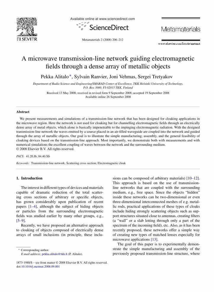
The transmission-line network that is used here ishe same as designed in Ref. [10], with the optimalmpedance matching with free space observed aroundhe frequency of 5.5 GHz. For this design, the match-ng with free space and the cloaking phenomenon wereerified with full-wave simulations [10]. In this papere demonstrate the simple manufacturing and assemblyf this type of structure with a two-dimensional peri-dic transmission-line network having a square shapend 16 × 16 unit cells in the network. The edges of theetwork are connected to a “transition layer” composedf parallel metal strips gradually enlarging from the endsf the network, as proposed in Ref. [10]. The function ofhis layer is to capture the fields propagating in free spacend transform these modes to the propagating modes ofhe transmission-line network. Thus, the layer can beonsidered as a mode-transforming device.
By inserting the designed network inside a metallicarallel-plate waveguide (with the plates lying in the xy-lane), we effectively realize the same situation as wouldccur with an infinitely periodic array of networks withhe periodicity along the z-axis, since here the electricelds are assumed to be normal to waveguide plates, as
n the example case that was studied previously [10]. Seeig. 1 for an illustration of the transmission-line network.
The structure shown in Fig. 1 was manufactured by
tching from a thin copper plate. The network can beimply assembled from two similar profiles (each pro-le as shown in Fig. 1a) just by placing them on topf each other, as shown in Fig. 1b. Ideally, the vol-Fig. 1. Illustration of the designed transmission-line network. (a) Net-work in the xy-plane. (b) Network in the yz-plane.
ume between these two metal objects should be freespace [10]. Here, due to practical reasons, we haveplaced small pieces of styrofoam, with material prop-erties very close to those of free space, between themetal strips. For assembly purposes, pieces of styro-foam are placed also on top and below the metal stripsfor support. These styrofoam pieces naturally do notaffect the propagation properties of the transmissionlines since the fields are mostly confined between theparallel strips.
In Ref. [10] the reference object, i.e., the object thatwe wanted to cloak (hide) from the surrounding electro-magnetic fields, was an array of infinitely long perfectlyconducting rods that fit inside the network of transmis-sion lines. Here we use a similar periodic structure asa reference object through which we want to guide thefields. The individual inclusions of this reference objectare metal cylinders (parallel to the z-axis) with the sameheight as the network (∼13 mm). The diameter of thesecylinders is 4 mm and there are a total of 15 × 15 = 225cylinders in the array.
3. Measurement setup
The measurement setup that is used here is similar tothe one presented in Ref. [4]. With our measurements
materia
approximately at 3 mm on top of the metal mesh. Theprobe is intentionally poorly matched at the frequen-cies of interest (5–6 GHz) in order to make sure thatthe measurement probe does not disturb the fields inside
208 P. Alitalo et al. / Meta
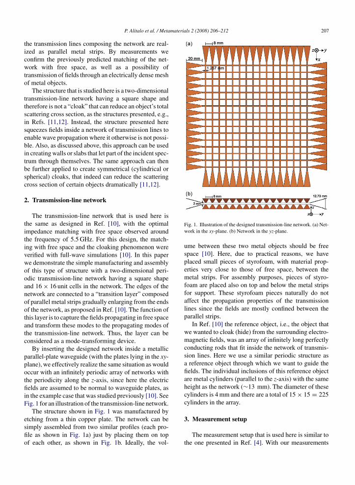
we effectively simulate an infinitely periodic structurewith the periodicity in the vertical (z-) direction, byintroducing a measurement cell consisting of a parallel-plate waveguide with its metallic plates lying in thexy-plane. Because of the image principle (the electricfields are assumed to be parallel to the z-axis inside thewaveguide), we can thus measure only one period of avolumetric structure. The difference between the mea-surement setup used here and the one in Ref. [4] is thathere the upper plate of the waveguide is formed by adense wire mesh, that lets through a fraction of the fieldinside the waveguide, instead of having a solid metal-lic upper plate with a hole for the probe, as was usedin Ref. [4]. The mesh that we use here is the same asthe one used in Ref. [14], i.e., the mesh is a thin copperplate, in which square holes of size 4 mm × 4 mm havebeen etched with the period of the holes being 5 mm.A small part of the field gets through this mesh and wecan measure that field with a probe placed on top of thewaveguide [14].
We excite a cylindrical wave in the waveguide with acoaxial feed probe placed inside the waveguide and mea-sure the transmission from this probe to the measurement
probe placed on top of the waveguide, with a vector net-work analyzer (VNA, Agilent E8363A). The use of themetal mesh as a part of the top plate of the waveguide,rather than using a probe inside the waveguide, ensuresFig. 2. Illustration of the measurement setup. (a) Waveguide with ametal mesh in the upper plate. (b) Measurement system with a VNAconnected to the feed and measurement probes (the measurement probeis stationary) and a PC controlling the scanner which moves the waveg-uide in x- and y-directions.
ls 2 (2008) 206–212
that the measurement probe does not disturb the fieldsinside the waveguide. The measurement probe on top ofthe waveguide is stationary, and the whole waveguide ismoved with a PC-controlled scanner, synchronized withthe VNA for precise measurements in the wanted coor-dinate positions. These points where the measurement ofthe complex S21-parameter are taken with the VNA, canbe arbitrarily chosen with the PC-program running thescanner. All the measurements presented in this paperwere done with the steps of 5 mm. As the measuredarea is 240 mm × 100 mm, we will have the complexS21 measured at 49 × 21 = 1029 different points in thexy-plane.
The measurement probe that we use here is amonopole oriented along the z-axis and positioned
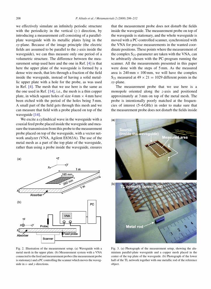
Fig. 3. (a) Photograph of the measurement setup, showing the alu-minium parallel-plate waveguide and a copper mesh placed in thecenter of the top plate of the waveguide. (b) Photograph of the lowerhalf of the TL network together with one metallic rod of the referenceobject.
materia
tmtp
ToebotwtiullhtttmTx
dStiaau
iAtaiG
4
a1tiooto
s
frequencies, where it makes sense to compare the fielddistributions, the wavefronts emanating from the sourceare strongly reflected at the front boundary of the refer-
P. Alitalo et al. / Meta
he waveguide. The high dynamic range of the VNAakes sure that we can measure the electric field distribu-
ion inside the waveguide even with this poorly matchedrobe.
See Fig. 2 for an illustration of the measurement setup.he parallel-plate waveguide has the width and lengthf 1 m, and the height h = 13 mm. Ideally h should bequal to 12.73 mm [10], but the height was chosen toe exactly 13 mm because of assembly issues. A partf the solid upper plate is removed from the center forhe placing of the metal mesh (the area above whiche want to measure the field distributions). The area of
his mesh is 260 mm × 185 mm. The measurable areas further restricted by the scanners moving the waveg-ide. We have used two scanners, one with the movementimited to 300 mm (x-axis) and one with the movementimited to 100 mm (y-axis). The area to be measuredas been decided to be 240 mm × 100 mm, centered inhe mesh area. The feed probe is positioned in the cen-er of the mesh along the y-direction and just outsidehe measured area in the x-direction, in order to have
ore space between the measured area and the feed.he feed probe coordinates are therefore decided to be= 250 mm, y = 50 mm, with the origin of this coor-
inate system being in one corner of the measured area.ee Fig. 3 for a photograph of the measurement setup,
aken from the direction of the positive z-axis, show-ng the empty waveguide and the metal mesh inserteds a part of the upper plate. The feed probe positionnd the measured area are also illustrated in the fig-re.
The volume between the waveguide plates, surround-ng the metal mesh, is filled by a microwave absorber.
large size of the waveguide ensures that the reflec-ions from the waveguide edges are minimized. Thebsorber thickness in the x- and y-directions is approx-mately five wavelengths or more at the frequency of 5Hz.
. Measurement results
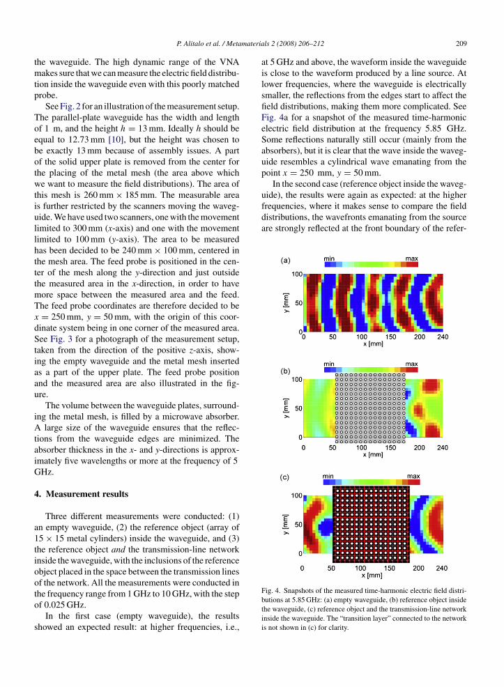
Three different measurements were conducted: (1)n empty waveguide, (2) the reference object (array of5 × 15 metal cylinders) inside the waveguide, and (3)he reference object and the transmission-line networknside the waveguide, with the inclusions of the referencebject placed in the space between the transmission linesf the network. All the measurements were conducted in
he frequency range from 1 GHz to 10 GHz, with the stepf 0.025 GHz.In the first case (empty waveguide), the resultshowed an expected result: at higher frequencies, i.e.,
ls 2 (2008) 206–212 209
at 5 GHz and above, the waveform inside the waveguideis close to the waveform produced by a line source. Atlower frequencies, where the waveguide is electricallysmaller, the reflections from the edges start to affect thefield distributions, making them more complicated. SeeFig. 4a for a snapshot of the measured time-harmonicelectric field distribution at the frequency 5.85 GHz.Some reflections naturally still occur (mainly from theabsorbers), but it is clear that the wave inside the waveg-uide resembles a cylindrical wave emanating from thepoint x = 250 mm, y = 50 mm.
In the second case (reference object inside the waveg-uide), the results were again as expected: at the higher
Fig. 4. Snapshots of the measured time-harmonic electric field distri-butions at 5.85 GHz: (a) empty waveguide, (b) reference object insidethe waveguide, (c) reference object and the transmission-line networkinside the waveguide. The “transition layer” connected to the networkis not shown in (c) for clarity.
210 P. Alitalo et al. / Metamaterials 2 (2008) 206–212
a) emptphase
torts the waveform. Note that the previously simulated“cloak slab” [10] was much wider and also thinner thanthe network measured here.
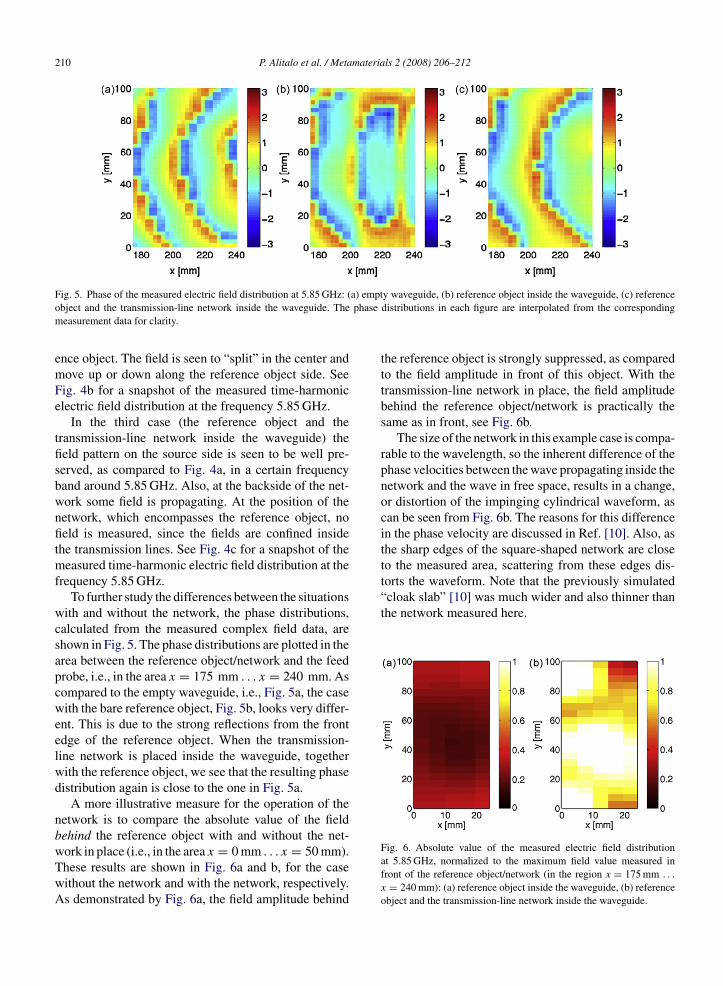
Fig. 5. Phase of the measured electric field distribution at 5.85 GHz: (object and the transmission-line network inside the waveguide. Themeasurement data for clarity.
ence object. The field is seen to “split” in the center andmove up or down along the reference object side. SeeFig. 4b for a snapshot of the measured time-harmonicelectric field distribution at the frequency 5.85 GHz.
In the third case (the reference object and thetransmission-line network inside the waveguide) thefield pattern on the source side is seen to be well pre-served, as compared to Fig. 4a, in a certain frequencyband around 5.85 GHz. Also, at the backside of the net-work some field is propagating. At the position of thenetwork, which encompasses the reference object, nofield is measured, since the fields are confined insidethe transmission lines. See Fig. 4c for a snapshot of themeasured time-harmonic electric field distribution at thefrequency 5.85 GHz.
To further study the differences between the situationswith and without the network, the phase distributions,calculated from the measured complex field data, areshown in Fig. 5. The phase distributions are plotted in thearea between the reference object/network and the feedprobe, i.e., in the area x = 175 mm . . . x = 240 mm. Ascompared to the empty waveguide, i.e., Fig. 5a, the casewith the bare reference object, Fig. 5b, looks very differ-ent. This is due to the strong reflections from the frontedge of the reference object. When the transmission-line network is placed inside the waveguide, togetherwith the reference object, we see that the resulting phasedistribution again is close to the one in Fig. 5a.
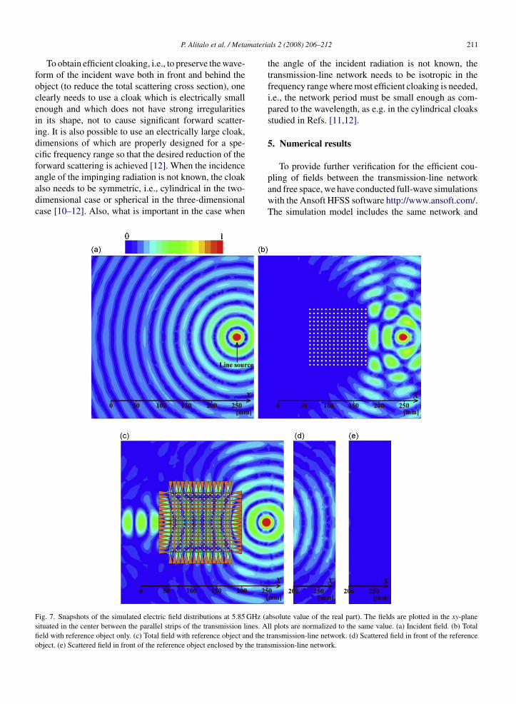
A more illustrative measure for the operation of thenetwork is to compare the absolute value of the fieldbehind the reference object with and without the net-
work in place (i.e., in the area x = 0 mm . . . x = 50 mm).These results are shown in Fig. 6a and b, for the casewithout the network and with the network, respectively.As demonstrated by Fig. 6a, the field amplitude behindy waveguide, (b) reference object inside the waveguide, (c) referencedistributions in each figure are interpolated from the corresponding
the reference object is strongly suppressed, as comparedto the field amplitude in front of this object. With thetransmission-line network in place, the field amplitudebehind the reference object/network is practically thesame as in front, see Fig. 6b.
The size of the network in this example case is compa-rable to the wavelength, so the inherent difference of thephase velocities between the wave propagating inside thenetwork and the wave in free space, results in a change,or distortion of the impinging cylindrical waveform, ascan be seen from Fig. 6b. The reasons for this differencein the phase velocity are discussed in Ref. [10]. Also, asthe sharp edges of the square-shaped network are closeto the measured area, scattering from these edges dis-
Fig. 6. Absolute value of the measured electric field distributionat 5.85 GHz, normalized to the maximum field value measured infront of the reference object/network (in the region x = 175 mm . . .
x = 240 mm): (a) reference object inside the waveguide, (b) referenceobject and the transmission-line network inside the waveguide.
materia
foceiidcfaadc
Fsfio
P. Alitalo et al. / Meta
To obtain efficient cloaking, i.e., to preserve the wave-orm of the incident wave both in front and behind thebject (to reduce the total scattering cross section), onelearly needs to use a cloak which is electrically smallnough and which does not have strong irregularitiesn its shape, not to cause significant forward scatter-ng. It is also possible to use an electrically large cloak,imensions of which are properly designed for a spe-ific frequency range so that the desired reduction of theorward scattering is achieved [12]. When the incidence
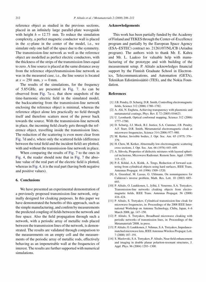
ngle of the impinging radiation is not known, the cloaklso needs to be symmetric, i.e., cylindrical in the two-imensional case or spherical in the three-dimensionalase [10–12]. Also, what is important in the case whenig. 7. Snapshots of the simulated electric field distributions at 5.85 GHz (aituated in the center between the parallel strips of the transmission lines. Aleld with reference object only. (c) Total field with reference object and the tbject. (e) Scattered field in front of the reference object enclosed by the tran
ls 2 (2008) 206–212 211
the angle of the incident radiation is not known, thetransmission-line network needs to be isotropic in thefrequency range where most efficient cloaking is needed,i.e., the network period must be small enough as com-pared to the wavelength, as e.g. in the cylindrical cloaksstudied in Refs. [11,12].
5. Numerical results
To provide further verification for the efficient cou-
pling of fields between the transmission-line networkand free space, we have conducted full-wave simulationswith the Ansoft HFSS software http://www.ansoft.com/.The simulation model includes the same network andbsolute value of the real part). The fields are plotted in the xy-planel plots are normalized to the same value. (a) Incident field. (b) Totalransmission-line network. (d) Scattered field in front of the referencesmission-line network.
materia
[
[
[
[matched microwave lens, IEEE Antennas Wireless Propagat. Lett.7 (2008) 187–191.
212 P. Alitalo et al. / Meta
reference object as studied in the previous sections,placed in an infinitely large parallel-plate waveguidewith height h = 12.73 mm. To reduce the simulationcomplexity, a perfect magnetic conductor wall is placedin the xz-plane in the center of the model, i.e., wesimulate only one half of the space due to the symmetry.The transmission-line network as well as the referenceobject are modelled as perfect electric conductors, withthe thickness of the strips of the transmission lines equalto zero. A line source is placed at the same distance awayfrom the reference object/transmission-line network aswas in the measured case, i.e., the line source is locatedat x = 250 mm, y = 0 mm.
The results of the simulations, for the frequencyof 5.85 GHz, are presented in Fig. 7. As can beobserved from Fig. 7a–c, that show snapshots of thetime-harmonic electric field in the simulated model,the backscattering from the transmission-line networkenclosing the reference object is minimal, whereas thereference object alone lets practically no field throughitself and therefore scatters most of the power backtowards the source. With the transmission-line networkin place, the incoming field clearly gets through the ref-erence object, travelling inside the transmission lines.The reduction of the scattering is even more clear fromFig. 7d and e, where only the scattered fields (differencebetween the total field and the incident field) are plotted,with and without the transmission-line network in place.
When comparing the results of Fig. 7 to the ones inFig. 4, the reader should note that in Fig. 7 the abso-lute value of the real part of the electric field is plotted,whereas in Fig. 4, it is the real part (having both negativeand positive values).
6. Conclusions
We have presented an experimental demonstration ofa previously proposed transmission-line network, orig-inally designed for cloaking purposes. In this paper wehave demonstrated the benefits of this approach, such asthe simple manufacturing, and confirm by measurementsthe predicted coupling of fields between the network andfree space. Also the field propagation through such anetwork, with a periodic array of metallic rods placedbetween the transmission lines of the network, is demon-strated. The results are validated through comparison tothe measurements on an empty cell and the measure-
ments of the periodic array of metallic rods, effectivelybehaving as an impenetrable wall at the frequencies ofinterest. The results are further supported with numericalsimulations.[
ls 2 (2008) 206–212
Acknowledgements
This work has been partially funded by the Academyof Finland and TEKES through the Center-of-Excellenceprogram and partially by the European Space Agency(ESA–ESTEC) contract no. 21261/07/NL/CB (Ariadnaprogram). The authors wish to thank Mr. E. Kahraand Mr. L. Laakso for valuable help with manu-facturing of the prototype and with building of themeasurement setup. P. Alitalo acknowledges financialsupport by the Finnish Graduate School in Electron-ics, Telecommunications, and Automation (GETA),Tekniikan Edistämissäätiö (TES), and the Nokia Foun-dation.
References
[1] J.B. Pendry, D. Schurig, D.R. Smith, Controlling electromagneticfields, Science 312 (2006) 1780–1782.
[2] A. Alú, N. Engheta, Achieving transparency with plasmonic andmetamaterial coatings, Phys. Rev. E 72 (2005) 016623.
[3] U. Leonhardt, Optical conformal mapping, Science 312 (2006)1777–1780.
[4] D. Schurig, J.J. Mock, B.J. Justice, S.A. Cummer, J.B. Pendry,A.F. Starr, D.R. Smith, Metamaterial electromagnetic cloak atmicrowave frequencies, Science 314 (2006) 977–980.
[5] M. Kerker, Invisible bodies, J. Opt. Soc. Am. 65 (1975) 376–379.
[6] H. Chew, M. Kerker, Abnormally low electromagnetic scatteringcross sections, J. Opt. Soc. Am. 66 (1976) 445–449.
[7] A. Sihvola, Properties of dielectric mixtures with layered spheri-cal inclusions, Microwave Radiomet. Remote Sens. Appl. (1989)115–123.
[8] P.-S. Kildal, A.A. Kishk, A. Tengs, Reduction of forward scat-tering from cylindrical objects using hard surfaces, IEEE Trans.Antennas Propagat. 44 (1996) 1509–1520.
[9] A. Greenleaf, M. Lassas, G. Uhlmann, On nonuniqueness forCalderon’s inverse problem, Math. Res. Lett. 10 (2003) 685–693.
10] P. Alitalo, O. Luukkonen, L. Jylhä, J. Venermo, S.A. Tretyakov,Transmission-line networks cloaking objects from electro-magnetic fields, IEEE Trans. Antennas Propagat. 56 (2008)416–424.
11] P. Alitalo, S. Tretyakov, Cylindrical transmission-line cloak formicrowave frequencies, in: Proceedings of the 2008 IEEE Inter-national Workshop on Antenna Technology, Chiba, Japan, 4–6March 2008, pp. 147–150.
12] P. Alitalo, S. Tretyakov, Broadband microwave cloaking withperiodic networks of transmission lines, in: Proceedings of theMetamaterials’2008, in press.
13] P. Alitalo, O. Luukkonen, J. Vehmas, S.A. Tretyakov, Impedance-
14] S. Maslovski, S.A. Tretyakov, P. Alitalo, Near-field enhancementand imaging in double planar polariton-resonant structures, J.Appl. Phys. 96 (2004) 1293–1300.