parallel-plate micro servo for probe-based data storage
TRANSCRIPT
Parallel-Plate Micro Servo for Probe-Based Data Storage
by
Michael Shiang-Cheng Lu
B.S. (National Tsing Hua University) 1991M.S. (National Tsing Hua University) 1993
A dissertation submitted in partial satisfaction of the requirements for the degree of
Doctor of Philosophy
in
Electrical and Computer Engineering
in the
Carnegie Institute of Technology
of the
Carnegie Mellon University
Committee:
Professor Gary K. Fedder, AdvisorProfessor L. Richard CarleyProfessor James A. BainDr. Storrs Hoen (Agilent, Inc.)
2002


Parallel-Plate Micro Servo for Probe-Based Data Storage
2002
by
Michael Shiang-Cheng Lu


To my parents,
to Chun-Yen, Chun-Zho, and Chun-Yi,
and to my wife Ching-Yu.


Abstract
Parallel-Plate Micro Servo for Probe-Based Data Storage
by
Michael Shiang-Cheng Lu
Doctor of Philosophy in Electrical and Computer Engineering
Carnegie Mellon University
Professor Gary K. Fedder, Advisor
This thesis describes the use of closed-loop voltage control to extend the travel range
of a parallel-plate electrostatic microactuator beyond the open-loop pull-in limit of one
third of the gap. A general controller design procedure is presented to deal with the nonlin-
earities and unstable characteristic of the parallel-plate actuator. The resulting linear con-
troller design is implemented easily for the desired application of a probe-based mass data
storage device. In the envisioned data storage system, an array of parallel-plate tip actua-
tors are employed to position the read/write probe tips about 10 nm away from the mag-
netic media for data access. Fabrication of tip actuators and servo and data channel circuits
are conveniently integrated by use of the CMOS-MEMS micromachining process devel-
oped at Carnegie Mellon.
Controller design ensures system stability in the presence of a unstable pole beyond
the pull-in limit. Desired transient response is achieved by a pre-filter added in front of the
feedback loop to shape the step input command. The fabricated microactuator is character-
ized by static and dynamic measurements, with a spring constant of 0.17 N/m, mechanical
resonant frequency of 12.4 kHz, and effective damping ratio from 0.55 to 0.35 for gaps
between 2.3 to 2.65 µm. The minimum input-referred noise capacitance change is 0.5 aF/
i

√Hz measured at a gap of 5.7 µm, corresponding to a minimum input-referred noise dis-
placement of 0.33 nm/√Hz. Measured closed-loop step response illustrates a maximum
travel distance up to 60% of the initial gap with a rise time less than 5 ms.
ii

Contents
List of Figures v
List of Tables x
1 Introduction 1
2 Electrostatic Gap Models 92.1 Introduction . . . . . . . . . . . . . . . . . . . . . . . . . . . . . . . . . . . . . . . . . . . . . . . . . . . . . 92.2 Electrostatic Force . . . . . . . . . . . . . . . . . . . . . . . . . . . . . . . . . . . . . . . . . . . . . . . 102.3 Gap Modeling . . . . . . . . . . . . . . . . . . . . . . . . . . . . . . . . . . . . . . . . . . . . . . . . . . 142.4 Simulation . . . . . . . . . . . . . . . . . . . . . . . . . . . . . . . . . . . . . . . . . . . . . . . . . . . . . 192.5 Experiment . . . . . . . . . . . . . . . . . . . . . . . . . . . . . . . . . . . . . . . . . . . . . . . . . . . . 21
3 Plant Design and Modeling 233.1 Introduction . . . . . . . . . . . . . . . . . . . . . . . . . . . . . . . . . . . . . . . . . . . . . . . . . . . . 233.2 CMOS-MEMS Fabrication . . . . . . . . . . . . . . . . . . . . . . . . . . . . . . . . . . . . . . . . 233.3 Material Property Characterization . . . . . . . . . . . . . . . . . . . . . . . . . . . . . . . . . . 29
3.3.1 Effective Young’s Modulus . . . . . . . . . . . . . . . . . . . . . . . . . . . . . . . . . 293.3.2 Residual Stress and Vertical Stress Gradient . . . . . . . . . . . . . . . . . . . . 313.3.3 Cyclic Fatigue . . . . . . . . . . . . . . . . . . . . . . . . . . . . . . . . . . . . . . . . . . . . 33
3.4 Parallel-Plate Microactuator Design . . . . . . . . . . . . . . . . . . . . . . . . . . . . . . . . . 353.4.1 Dynamic Equation . . . . . . . . . . . . . . . . . . . . . . . . . . . . . . . . . . . . . . . . . 353.4.2 Design Description . . . . . . . . . . . . . . . . . . . . . . . . . . . . . . . . . . . . . . . . 373.4.3 Spring Constant . . . . . . . . . . . . . . . . . . . . . . . . . . . . . . . . . . . . . . . . . . . 413.4.4 Modal Analysis . . . . . . . . . . . . . . . . . . . . . . . . . . . . . . . . . . . . . . . . . . . 473.4.5 Squeeze-Film Damping . . . . . . . . . . . . . . . . . . . . . . . . . . . . . . . . . . . . . 54
3.5 Capacitive Position Sensing . . . . . . . . . . . . . . . . . . . . . . . . . . . . . . . . . . . . . . . 603.5.1 Pre-amp Circuit Design . . . . . . . . . . . . . . . . . . . . . . . . . . . . . . . . . . . . . 633.5.2 Double-Balanced Demodulator . . . . . . . . . . . . . . . . . . . . . . . . . . . . . . . 70
3.6 Noise Analysis and Minimum Detectable Signal . . . . . . . . . . . . . . . . . . . . . . . 723.6.1 Pre-amp Noise . . . . . . . . . . . . . . . . . . . . . . . . . . . . . . . . . . . . . . . . . . . . 723.6.2 Brownian Noise . . . . . . . . . . . . . . . . . . . . . . . . . . . . . . . . . . . . . . . . . . . 77
4 Controller Design 794.1 Introduction . . . . . . . . . . . . . . . . . . . . . . . . . . . . . . . . . . . . . . . . . . . . . . . . . . . . 794.2 Classical Frequency-Domain Feedback Theory. . . . . . . . . . . . . . . . . . . . . . . . . 79
4.2.1 Quantification of Feedback Performance. . . . . . . . . . . . . . . . . . . . . . . . 804.2.2 Analysis of Unstable Plant . . . . . . . . . . . . . . . . . . . . . . . . . . . . . . . . . . 82
4.2.2.1 Stability Criterion . . . . . . . . . . . . . . . . . . . . . . . . . . . . . . . . . . 824.2.2.2 Bandwidth Limitations with a Real Unstable Pole . . . . . . . . . 83
iii

4.2.2.3 Unstable Poles and the Sensitivity Function . . . . . . . . . . . . . . 854.2.2.4 Unstable Poles and the Complementary Sensitivity Function 87
4.3 Controller Design by Linearization . . . . . . . . . . . . . . . . . . . . . . . . . . . . . . . . . . 894.3.1 Two-Degree-of-Freedom Control Systems . . . . . . . . . . . . . . . . . . . . . . 894.3.2 Closed-Loop Step Response . . . . . . . . . . . . . . . . . . . . . . . . . . . . . . . . . 904.3.3 Plant Linearization . . . . . . . . . . . . . . . . . . . . . . . . . . . . . . . . . . . . . . . . . 954.3.4 Phase-Margin Optimization using a Proportional-Gain Controller . . . . 98
4.3.4.1 Plant in the Unstable Regime . . . . . . . . . . . . . . . . . . . . . . . . . 994.3.4.2 Plant in the Stable Regime . . . . . . . . . . . . . . . . . . . . . . . . . . . 103
4.3.5 Plant Input Disturbance Rejection . . . . . . . . . . . . . . . . . . . . . . . . . . . . 1094.3.5.1 Problem Formulation . . . . . . . . . . . . . . . . . . . . . . . . . . . . . . 1094.3.5.2 Controller Design . . . . . . . . . . . . . . . . . . . . . . . . . . . . . . . . . 111
4.3.6 Steady-State Error . . . . . . . . . . . . . . . . . . . . . . . . . . . . . . . . . . . . . . . . 1144.3.7 Shock Rejection . . . . . . . . . . . . . . . . . . . . . . . . . . . . . . . . . . . . . . . . . . 116
4.4 Controller Design by the QFT (Quantitative Feedback Theory) Method . . . . 1194.4.1 Generation of Bounds . . . . . . . . . . . . . . . . . . . . . . . . . . . . . . . . . . . . . 1204.4.2 Modification of Bounds and Loop Shaping . . . . . . . . . . . . . . . . . . . . 1234.4.3 Plant Input Disturbance Rejection . . . . . . . . . . . . . . . . . . . . . . . . . . . . 128
4.5 Scaling of Plant Parameters . . . . . . . . . . . . . . . . . . . . . . . . . . . . . . . . . . . . . . . 129
5 Experimental Results 1355.1 Introduction . . . . . . . . . . . . . . . . . . . . . . . . . . . . . . . . . . . . . . . . . . . . . . . . . . . 1355.2 Experimental Setup . . . . . . . . . . . . . . . . . . . . . . . . . . . . . . . . . . . . . . . . . . . . . 1355.3 Curl Measurement . . . . . . . . . . . . . . . . . . . . . . . . . . . . . . . . . . . . . . . . . . . . . . 1375.4 Static Characterization . . . . . . . . . . . . . . . . . . . . . . . . . . . . . . . . . . . . . . . . . . . 1395.5 Capacitive Feedthrough . . . . . . . . . . . . . . . . . . . . . . . . . . . . . . . . . . . . . . . . . . 1405.6 Open-Loop Frequency Response . . . . . . . . . . . . . . . . . . . . . . . . . . . . . . . . . . . 1415.7 Open-Loop Step Response . . . . . . . . . . . . . . . . . . . . . . . . . . . . . . . . . . . . . . . 1435.8 Input-Referred Noise Displacement . . . . . . . . . . . . . . . . . . . . . . . . . . . . . . . . 1465.9 Closed-Loop Step Response . . . . . . . . . . . . . . . . . . . . . . . . . . . . . . . . . . . . . . 1485.10 Discussion . . . . . . . . . . . . . . . . . . . . . . . . . . . . . . . . . . . . . . . . . . . . . . . . . . . . 150
6 Conclusions 1576.1 Future Work . . . . . . . . . . . . . . . . . . . . . . . . . . . . . . . . . . . . . . . . . . . . . . . . . . . 159
Bibliography 161
Appendix A Electrostatic Gap Model 173
Appendix B Control System Electronics 177
iv

List of Figures
1.1 Schematic representation of the envisioned micro disk drive. . . . . . . . . . . . . . . . . . 41.2 Top view and side view of the read/write probe head design. . . . . . . . . . . . . . . . . . 41.3 Side view of the bonded media-actuator die and the tip-actuator die, illustrating non-
uniform gaps resulted from a tilted media and curl variations of tip actuators. . . . . 61.4 Schematic representation of the feedback system using a frequency-multiplexed
scheme to separate the actuation and sensing signals. Frequency responses in the plotillustrate the frequency components of signals at each node inside the loop. . . . . . 7
2.1 Schematic of two charged conductors. . . . . . . . . . . . . . . . . . . . . . . . . . . . . . . . . . . 102.2 Path of integration in variable space. (a) For evaluating energy We. (b) For evaluating
coenergy We’. . . . . . . . . . . . . . . . . . . . . . . . . . . . . . . . . . . . . . . . . . . . . . . . . . . . . . 112.3 Schematic of parallel-plate actuator. . . . . . . . . . . . . . . . . . . . . . . . . . . . . . . . . . . . . 132.4 Schematic of comb-finger actuator. (a) Top view. (b) Side view. . . . . . . . . . . . . . 132.5 Schematics of the electrode geometry for (a) two electrodes of the same width, (b)
two electrodes in which one is much wider than the other, and (c) comb fingers. 142.6 Capacitance per unit length as a function of g/h and θ for two electrodes of the same
width. . . . . . . . . . . . . . . . . . . . . . . . . . . . . . . . . . . . . . . . . . . . . . . . . . . . . . . . . . . . 152.7 Extracted Ki’s values plotted as a function of the w/h ratio and the sidewall angle θ.162.8 The distributed parallel-plate force is replaced by lumped forces applied at the ends
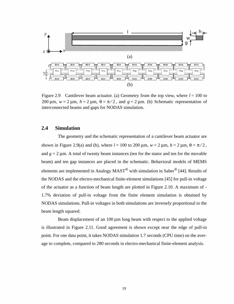
of beam models. . . . . . . . . . . . . . . . . . . . . . . . . . . . . . . . . . . . . . . . . . . . . . . . . . . . 182.9 Cantilever beam actuator. (a) Geometry from the top view, where l = 100 to 200 µm,
w = 2 µm, h = 2 µm, θ = π/2, and g = 2 µm. (b) Schematic representation of inter-connected beams and gaps for NODAS simulation. . . . . . . . . . . . . . . . . . . . . . . . 19
2.10 NODAS and electro-mechanical finite-element simulations of pull-in voltage forl = 100 to 200 µm, w = 2 µm, h = 2 µm, θ = π/2, and g = 2 µm. . . . . . . . . . . . . . . 20
2.11 Displacement-voltage characteristics from electro-mechanical finite-element andNODAS simulations for an 100µm-long beam actuator. . . . . . . . . . . . . . . . . . . . . 20
3.1 Cross section of the CMOS-MEMS process flow. (a) After CMOS processing. (b)After anisotropic dielectric reactive-ion etch for definition of structural sidewalls. (c)After anisotropic silicon etch. (d) After isotropic silicon etch for structural release.. . . . . . . . . . . . . . . . . . . . . . . . . . . . . . . . . . . . . . . . . . . . . . . . . . . . . . . . . . . . . . . . . 25
3.2 (a) Fabricated crab-leg comb-drive resonator using the Agilent 0.5 µm three-metal n-well process. (b) Beam cross-section with three metal layers, inter-metal dielectriclayers, and polysilicon. . . . . . . . . . . . . . . . . . . . . . . . . . . . . . . . . . . . . . . . . . . . . . . 26
3.3 Polymers stacked on beam sidewalls resulted from excessive polymerization duringdielectric RIE. . . . . . . . . . . . . . . . . . . . . . . . . . . . . . . . . . . . . . . . . . . . . . . . . . . . . . 26
3.4 Failure mechanisms of electrical connections: (a) opened vias, and (b) lateral etch ofrefractory Ti/W layers deposited on top and bottom of metal layers. . . . . . . . . . . 27
3.5 Resonant beam actuators for measuring effective Young’s modulus of compositebeams. . . . . . . . . . . . . . . . . . . . . . . . . . . . . . . . . . . . . . . . . . . . . . . . . . . . . . . . . . . . 29
3.6 (a) SEM of a m3-m2-m1 bent-beam strain sensor. (b) Thermal-mechanical finite-el-ement simulation by MEMCAD for residual stress analysis. . . . . . . . . . . . . . . . . 32
3.7 Uniform curl of local metal-3 and metal-1-3 beams. . . . . . . . . . . . . . . . . . . . . . . . 33
v

3.8 (a) SEM of a fan structure for durability test. (b) Measured frequency spectrum has alateral mode at 13.1 kHz and a out-of-plane mode at 11.2 kHz. . . . . . . . . . . . . . . 34
3.9 (a) Resonant frequency change of the fatigue structure with respect to the experi-enced cycles. (b) Side view of the notch before testing. (c) Broken notch after testing. . . . . . . . . . . . . . . . . . . . . . . . . . . . . . . . . . . . . . . . . . . . . . . . . . . . . . . . . . . . . . . . . . 35
3.10 (a) Schematic of parallel-plate actuator represented by a lumped-parameter model.(b) Free-body diagram illustrating the forces acting on the plate, including the elec-trostatic force, Fe, the damping force, Fd, and the spring restoring force, Fs. . . . . 36
3.11 Normalized displacement-voltage characteristic of parallel-plate actuator. . . . . . 383.12 (a) Schematic of tip actuator design for probe-based data storage. (b) to (f): Side view
at cross-section lines, illustrating electrical connections using three metal layers. 393.13 Side view schematic of actuator curl design. (a) Ends of springs are close to a straight
line between anchors in design. (b) Ends of springs are away from anchors in design. . . . . . . . . . . . . . . . . . . . . . . . . . . . . . . . . . . . . . . . . . . . . . . . . . . . . . . . . . . . . . . . . . 40
3.14 Schematic of tip actuator design. . . . . . . . . . . . . . . . . . . . . . . . . . . . . . . . . . . . . . 423.15 Free-body diagram of one half of actuator used for deriving z-directional spring con-
stant. . . . . . . . . . . . . . . . . . . . . . . . . . . . . . . . . . . . . . . . . . . . . . . . . . . . . . . . . . . . . 433.16 Comparison of analytic z-directional spring constants with finite-element analysis.
. . . . . . . . . . . . . . . . . . . . . . . . . . . . . . . . . . . . . . . . . . . . . . . . . . . . . . . . . . . . . . . . . 46 3.17 Twelve-degree-of-freedom beam finite element. . . . . . . . . . . . . . . . . . . . . . . . . . 483.18 Transformation of a beam element from local to global (x, y) coordinates. . . . . . 503.19 Schematic of one half of the actuator represented by beam elements for finite-ele-
ment modal analysis. Nodes are numbered from 1 to 2n + 6, with n representing thenumber of connector beams. . . . . . . . . . . . . . . . . . . . . . . . . . . . . . . . . . . . . . . . . . 51
3.20 Comparison of z-directional eigenmodes with numerical finite-element analysis. 543.21 Illustration of the first three modes of the actuator by numerical finite-element anal-
ysis. . . . . . . . . . . . . . . . . . . . . . . . . . . . . . . . . . . . . . . . . . . . . . . . . . . . . . . . . . . . . . 553.22 Cross-section schematic illustrating a squeezed thin film of gas between two parallel
plates separated by a gap, g, resulted from the vertical motion of the plate with veloc-ity, v. The squeeze-film damping force, FD, is produced opposing the direction ofmotion. . . . . . . . . . . . . . . . . . . . . . . . . . . . . . . . . . . . . . . . . . . . . . . . . . . . . . . . . . . 56
3.23 Equivalent circuit model using nonlinear inductors and resistors for squeeze-filmdamping analysis. Damping force and plate velocity are analogous to electrical cur-rent and voltage in the schematic. . . . . . . . . . . . . . . . . . . . . . . . . . . . . . . . . . . . . . 57
3.24 Schematic of lumped-parameter actuator model driven by a sinusoidal force sourcefor frequency-domain analysis. Squeeze-film damping forces of the three plates indesign are modelled separately due to their different displacements and velocities.. . . . . . . . . . . . . . . . . . . . . . . . . . . . . . . . . . . . . . . . . . . . . . . . . . . . . . . . . . . . . . . . . . . 59
3.25 Damping ratio of parallel-plate actuator versus gap separation at atmospheric pres-sure. . . . . . . . . . . . . . . . . . . . . . . . . . . . . . . . . . . . . . . . . . . . . . . . . . . . . . . . . . . . . 60
3.26 (a) Side-view schematic of parallel-plate actuator illustrating capacitive sensingscheme. (b) Equivalent capacitive sensing circuit model. . . . . . . . . . . . . . . . . . . . 61
3.27 (a) Schematic of sensing pre-amp using an operational amplifier in a non-invertingamplifier configuration. The bias transistor operates in the sub-threshold region to actas a large resistance. (b) Schematic of folded-cascode operational amplifier with acommon-source amplifier as the output stage. . . . . . . . . . . . . . . . . . . . . . . . . . . . . 64
vi

3.28 Schematic of the constant-transconductance bias circuit for the folded-cascode am-plifier. . . . . . . . . . . . . . . . . . . . . . . . . . . . . . . . . . . . . . . . . . . . . . . . . . . . . . . . . . . . 67
3.29 Frequency response of the sensing pre-amp. Measured d.c. gain is 9.85, and the -3 dBfrequency is 5.7 MHz. . . . . . . . . . . . . . . . . . . . . . . . . . . . . . . . . . . . . . . . . . . . . . . 69
3.30 Measured resistance of subthreshold biasing transistor versus gate-to-source voltage. . . . . . . . . . . . . . . . . . . . . . . . . . . . . . . . . . . . . . . . . . . . . . . . . . . . . . . . . . . . . . . . . . 70
3.31 Gilbert multiplier with emitter degeneration applied to improve input voltage range. . . . . . . . . . . . . . . . . . . . . . . . . . . . . . . . . . . . . . . . . . . . . . . . . . . . . . . . . . . . . . . . . . 71
3.32 Equivalent pre-amp noise model. . . . . . . . . . . . . . . . . . . . . . . . . . . . . . . . . . . . . . . 733.33 (a) Minimum input-referred noise capacitance change versus gap. (b) Minimum in-
put-referred noise displacement versus gap. . . . . . . . . . . . . . . . . . . . . . . . . . . . . . 763.34 Equivalent Brownian noise displacement of the micromechanical actuator and equiv-
alent noisedisplacement derived from preamp noise plotted as a function of gap. 784.1 Block diagram of a linear time-invariant feedback system. Adequate controller de-
sign rejects input and output disturbances (d1, d2), and avoids noise (n) amplification. . . . . . . . . . . . . . . . . . . . . . . . . . . . . . . . . . . . . . . . . . . . . . . . . . . . . . . . . . . . . . . . . . 80
4.2 (a) The notion of crossing with the ray between (-∞, -1 + j0] on the complex plane.(b) The notion of crossing on the Nichols chart, where the ray is defined as R1= dB. . . . . . . . . . . . . . . . . . . . . . . . . . . . . . . . . . . . . . . 83
4.3 Graphical illustration of the sensitivity function magnitude for L(s) having at leasttwo more poles than zeros. Sensitivity is larger than one when L(s) enters the unit cir-cle centered at -1 + j0. . . . . . . . . . . . . . . . . . . . . . . . . . . . . . . . . . . . . . . . . . . . . . . 85
4.4 Minimum complementary sensitivity peak versus ratio of crossover frequency to un-stable pole frequency. A rule of thumb for design requires that the crossover frequen-cy at least twice as large as the unstable pole frequency with an one-pole rolloff toreduce resultant peak within 4 dB. . . . . . . . . . . . . . . . . . . . . . . . . . . . . . . . . . . . . . 88
4.5 Two-degree-of-freedom control system configuration. Sensitivity reduction and dis-turbance rejection are performed inside the loop by C(s), and tracking performanceis achieved by design of F(s). . . . . . . . . . . . . . . . . . . . . . . . . . . . . . . . . . . . . . . . . . 90
4.6 Percentage ratio of the voltage difference between the transient and steady-state re-sponses as a function of normalized displacement. (a) tracking bandwidthωb = 0.05ωn to 0.2ωn. (b) tracking bandwidth ωb = 0.25ωn to ωn. . . . . . . . . . . . . 94
4.7 Ratio of maximum applied voltage over static pull-in voltage versus ratio of trackingbandwidth over actuator bandwidth. . . . . . . . . . . . . . . . . . . . . . . . . . . . . . . . . . . . 95
4.8 The d.c. actuator gain as a function of normalized displacement. At α = 1/3, the ac-tuator acts like a “mechanical integrator” with an infinite d.c. gain. . . . . . . . . . . . 97
4.9 The nonlinear plant is replaced by a set of linearized plants at different operatingpoints. . . . . . . . . . . . . . . . . . . . . . . . . . . . . . . . . . . . . . . . . . . . . . . . . . . . . . . . . . . . 98
4.10 With one unstable pole, L(s) must start from -180° on the Nichols chart to result in astable system, thereby producing a finite lower gain margin. . . . . . . . . . . . . . . . 100
4.11 Flow chart for LTI proportional-gain controller design for a set of linearized unstableplants. Final controller design kp must ensure adequate phase and gain margins for allthe linearized plants. . . . . . . . . . . . . . . . . . . . . . . . . . . . . . . . . . . . . . . . . . . . . . . . 104
4.12 Maximum phase margin, and corresponding crossover frequency, lower gain margin,upper gain margin and controller gain are plotted from (a) to (e) as a function of nor-malized displacement. Selected LTI controller is kp = 16 which gives a minimum
φ r,( ) φ 180– ° r 0>,=
vii

phase margin around 60° at all displacements. . . . . . . . . . . . . . . . . . . . . . . . . . . 1054.13 (a) Effective damping ratio as a function of normalized displacement. (b) Ratio of ef-
fective resonant frequency over mechanical resonant frequency as a function of nor-malized displacement. . . . . . . . . . . . . . . . . . . . . . . . . . . . . . . . . . . . . . . . . . . . . . 106
4.14 (a) Open-loop transfer function of LTV design on the Nichols chart. (b) Open-looptransfer function of LTI design on the Nichols chart. . . . . . . . . . . . . . . . . . . . . . . 107
4.15 Maximum controller gain kp versus normalized plate displacement by stability re-quirement. . . . . . . . . . . . . . . . . . . . . . . . . . . . . . . . . . . . . . . . . . . . . . . . . . . . . . . . 108
4.16 Ratio of disturbance force over first-order electrostatic force plotted as a function ofnormalized displacement for ∆z/Zo = 0.025 to 0.1. . . . . . . . . . . . . . . . . . . . . . . . 110
4.17 High-order terms of the electrostatic force expanded by the Taylor’s series are for-mulated as an input disturbance force. . . . . . . . . . . . . . . . . . . . . . . . . . . . . . . . . . 111
4.18 Perturbed displacement and voltage shown as an elliptical disc region around an op-erating point. . . . . . . . . . . . . . . . . . . . . . . . . . . . . . . . . . . . . . . . . . . . . . . . . . . . . . 112
4.19 Concept of asymptotically stable. . . . . . . . . . . . . . . . . . . . . . . . . . . . . . . . . . . . . 1124.20 The minimum controller gain plotted as a function of normalized displacement for
input disturbance rejection. Also plotted are the optimal gain from 4.12(e) for an LTVdesign, and the maximum applied gain to maintain a minimum phase margin of 20°.. . . . . . . . . . . . . . . . . . . . . . . . . . . . . . . . . . . . . . . . . . . . . . . . . . . . . . . . . . . . . . . . 114
4.21 System block diagram at equilibrium point z = Zo. . . . . . . . . . . . . . . . . . . . . . . . 1154.22 Percentage steady-state error as a function of normalized displacement. (kp = 16) .. .
. . . . . . . . . . . . . . . . . . . . . . . . . . . . . . . . . . . . . . . . . . . . . . . . . . . . . . . . . . . . . . . . 1164.23 System block diagram at a new equilibrium point z = Zo + ∆zs due to the external
shock force applied to the actuator. . . . . . . . . . . . . . . . . . . . . . . . . . . . . . . . . . . . 1174.24 Minimum required controller gain versus normalized displacement for suppressing
the induced displacement from an 150 g shock force to 100 nm, 10 nm, and 1 nm. .. . . . . . . . . . . . . . . . . . . . . . . . . . . . . . . . . . . . . . . . . . . . . . . . . . . . . . . . . . . . . . . . . 118
4.25 Flow chart for computing QFT bounds [82]. . . . . . . . . . . . . . . . . . . . . . . . . . . . 1224.26 Typical QFT bounds displayed on the Nichols chart for design of the loop transmis-
sion Lo(jω). (type I: line. Type II: closed contour.) . . . . . . . . . . . . . . . . . . . . . . 1234.27 (a) Templates of linearized unstable plants at various frequencies. (b) Robust stability
bounds derived for the nominal unstable plant. . . . . . . . . . . . . . . . . . . . . . . . . . 1244.28 New stability lines on the Nyquist plot (left) and the Nichols chart (right), derived for
unstable and/or non-minimum phase plants [84]. . . . . . . . . . . . . . . . . . . . . . . . . 1264.29 Robust stability bounds and stability lines derived for the new stable nominal plant.
. . . . . . . . . . . . . . . . . . . . . . . . . . . . . . . . . . . . . . . . . . . . . . . . . . . . . . . . . . . . . . . . 1274.30 Shaping of nominal open-loop function based on the derived bounds, such that
Lo’(jω) does not fall within the area as indicated in Figure 4.24. (kp = 30) . . . . . 1274.31 Input-disturbance bounds and loop-shaping result using kp = 106. . . . . . . . . . . . 1294.32 Maximum phase margin, and corresponding crossover frequency, lower gain margin,
upper gain margin and controller gain plotted as a function of normalized displace-ment from (a) to (e). . . . . . . . . . . . . . . . . . . . . . . . . . . . . . . . . . . . . . . . . . . . . . . . 132
5.1 Photograph of custom assembly for setting initial gap and static interferometric mea-surement. . . . . . . . . . . . . . . . . . . . . . . . . . . . . . . . . . . . . . . . . . . . . . . . . . . . . . . . 136
5.2 Schematic of custom interferometric setup for static-displacement measurement. La-ser alignment is used for adjusting parallelism between the gold-coated glass and the
viii

actuator die. . . . . . . . . . . . . . . . . . . . . . . . . . . . . . . . . . . . . . . . . . . . . . . . . . . . . . 1365.3 (a) SEM of released tip actuator fabricated by the AMS 0.5 µm CMOS process. (b)
Structural curl measured by the WYCO white-light interferometric profiler. . . . 1375.4 Side view schematic of the actuator. . . . . . . . . . . . . . . . . . . . . . . . . . . . . . . . . . . 1385.5 The static displacement-voltage characteristic measures the actuator spring constant
at 0.17 N/m. . . . . . . . . . . . . . . . . . . . . . . . . . . . . . . . . . . . . . . . . . . . . . . . . . . . . . 1395.6 Characteristic of pre-amp output versus plate displacement results in an extracted
pre-amp input capacitance of 333 fF. . . . . . . . . . . . . . . . . . . . . . . . . . . . . . . . . . . 1405.7 Schematic of capacitive sensing circuit, illustrating a sensed voltage error introduced
by capacitive feedthrough from actuation voltage, and reduction of feedthrough byhigh-pass filtering. . . . . . . . . . . . . . . . . . . . . . . . . . . . . . . . . . . . . . . . . . . . . . . . . 141
5.8 Measured frequency response of the actuator driven at different d.c. bias, illustratingthe resonant frequency shift due to the spring-softening effect. . . . . . . . . . . . . . 142
5.9 Measured resonant frequency versus d.c. actuation voltage. . . . . . . . . . . . . . . . . 1435.10 (a) Measured resonant peak and corresponding NODAS simulation results plotted as
a function of d.c. actuation voltage in the frequency-response measurement. (b) Ex-tracted effective damping ratio and corresponding NODAS simulation results plottedas a function of d.c. actuation voltage. . . . . . . . . . . . . . . . . . . . . . . . . . . . . . . . . 144
5.11 Open-loop responses to 2 kHz square-wave actuation force varying in applied volt-age amplitude from 1 V to 4.8 V (gap = 2.45 µm). . . . . . . . . . . . . . . . . . . . . . . . 145
5.12 Open-loop responses to 2 kHz square-wave actuation force varying in applied volt-age amplitude from 1 V to 7 V (gap = 3.2 µm). . . . . . . . . . . . . . . . . . . . . . . . . . . 146
5.13 (a) Pre-amp output spectrum measurement to a 2 kHz square-wave actuation voltagewith an amplitude of 0.2 V. (b) Measured input-referred sensed voltage as a functionof actuation gap. (c) Equivalent input-referred capacitance change as a function of ac-tuation gap. . . . . . . . . . . . . . . . . . . . . . . . . . . . . . . . . . . . . . . . . . . . . . . . . . . . . . . 147
5.14 Optical photograph of the PCB with the tip actuator package and off-chip feedbackcontrol circuit. . . . . . . . . . . . . . . . . . . . . . . . . . . . . . . . . . . . . . . . . . . . . . . . . . . . 148
5.15 (a) Measured controller output waveforms when displaced plate enters pull-in regionand beyond. The inset illustrates its waveform when the input command turns fromhigh to low. (b) Measured demodulated pre-amp output waveforms. (c) Plate dis-placement versus input command voltage. (gap = 3.3 µm) . . . . . . . . . . . . . . . . . 149
5.16 Schematic representation of parallel-plate actuator design for closed-loop NODASsimulation. . . . . . . . . . . . . . . . . . . . . . . . . . . . . . . . . . . . . . . . . . . . . . . . . . . . . . . 151
5.17 Measured waveforms (dashed lines) and simulated waveforms (solid lines) of pre-fil-ter output, controller output, demodulated pre-amp output, and plate displacement toa 50 Hz square-wave input-command voltage. . . . . . . . . . . . . . . . . . . . . . . . . . . 152
5.18 (a) Damping ratio derived from tilted plates and parallel plates as a function of nor-malized displacement. (b) Phase margin derived from tilted plates and parallel platesas a function of normalized displacement. . . . . . . . . . . . . . . . . . . . . . . . . . . . . . . 154
5.19 Noise gain from sensor output to controller output plotted for linearized plants at dif-ferent displacements. . . . . . . . . . . . . . . . . . . . . . . . . . . . . . . . . . . . . . . . . . . . . . . 155
B.1 Schematic of feedback control board. Controller gain kp = 24.3 is split into two parts(24.3 = 10 × 2.43). The gain of ten is placed after subtraction of the initial sensedvoltage. . . . . . . . . . . . . . . . . . . . . . . . . . . . . . . . . . . . . . . . . . . . . . . . . . . . . . . . . . 177
B.2 Schematic of demodulation circuit. . . . . . . . . . . . . . . . . . . . . . . . . . . . . . . . . . . . 178
ix

x
List of Tables2.1 Measured pull-in voltage of polysilicon beam actuators compared with NODAS and
electro-mechanical finite-element simulation results. . . . . . . . . . . . . . . . . . . . . . . 213.1 Measured effective Young’s modulus (in GPa) of composite beams from MOSIS
N78H-AV run. . . . . . . . . . . . . . . . . . . . . . . . . . . . . . . . . . . . . . . . . . . . . . . . . . . . . 313.2 Measured effective Young’s modulus (in GPa) of composite beams from N6CJ-AV
run and comparison with average values of N78H-AV run. . . . . . . . . . . . . . . . . . 313.3 Residual stress (in MPa) measured from MOSIS N78Q-AH, N79V-AQ, and N78H-
AV runs. . . . . . . . . . . . . . . . . . . . . . . . . . . . . . . . . . . . . . . . . . . . . . . . . . . . . . . . . . 323.4 Radius of curvatures (in mm) measured from dice of MOSIS N78Q-AH, N79V-AQ,
and N78H-AV runs. . . . . . . . . . . . . . . . . . . . . . . . . . . . . . . . . . . . . . . . . . . . . . . . . 343.5 Transistor dimensions in the folded-cascode amplifier design. . . . . . . . . . . . . . . . 663.6 Transistor dimensions in the constant-transconductance bias circuit. . . . . . . . . . . 685.1 Measured curl and plate tilt of the tip actuator. . . . . . . . . . . . . . . . . . . . . . . . . . . 1385.2 Open-loop risetime and fall measurements (gap = 2.45 µm). . . . . . . . . . . . . . . . 1435.3 Open-loop risetime and fall measurements (gap = 3.2 µm). . . . . . . . . . . . . . . . . 146

Acknowledgements
I would like to express my sincere gratitude to my research advisor, Professor Gary
K. Fedder, for his guidance, advice, and encouragement over the years of my research
work at Carnegie Mellon. I’ll always cherish those great memories of working with him
for the rest of my life! Many thanks to my other three thesis committee members, Profes-
sor L. Richard Carley, Professor James A. Bain, and Dr. Storrs Hoen for reviewing the
manuscript and giving me invaluable advice. I am grateful to Dr. Tamal Mukherjee for his
many research suggestions and help with simulation software, and to Professor Bill Mess-
ner for discussions on nonlinear control system.
I would like to thank many friends in the MEMS lab for their friendship, help, and
many discussions that have pushed my research forward. I am very grateful to Xu Zhu for
his help on chip-releases and taking those great-looking SEM photos, to Huikai for discus-
sions on many optical questions and help on fabrication, to Hasnain Lakdawala for discus-
sions on circuit design and feedback control, to Hao Luo for discussions on control circuit
implementation and PCB design, to Qi Jing, Jan Vandemeer, and Sitaraman Iyer for their
help on NODAS simulations, to Jiangfeng Wu and Gang Zhang for their many circuit
design insights, to Bikram Baiyda for his help on layout extraction, and to Kai He for his
Cadence support. I would like to thank many former and present officemates for the
numerous things that they have helped me with over the years: Michael Stout, Steven
Eagle, Dr. John Neumann, George Lopez, Lauren de Rosset, Dan Gaugel, Matthew
Zeleznik, Brett Diamond, Kevin Frederick, Nilmoni Deb, John Ramsey, Keith Rebello,
and Michael Kranz. Special thanks to Dr. Lars Erdmann for his help with the interferomet-
ric setup, which allowed me to complete the parallel-plate servo experiment.
xi

It has been a wonderful experience to work on the MEMS data storage project, and
to share expertise with many professors and fellow students (not mentioned elsewhere):
Dr. Art Davidson, Professor Dave Greve, Dr. David Guillou, Suresh Santhanam, Fernando
Alfaro, Seungook Min, Shan Liu, Xiaochun Wu, Li Zhang, and Rany El-Sayed. Many
thanks to the cleanroom staff, Chris Bowman, Robert Harris, and Carsen Kline for their
assistance which made our research work much easier.
Many thanks to Drew Danielson, and the MEMS lab administrator, Mary Moore,
who has been a tremendous help for me in so many things, and truly made my research life
a whole lot easier. I thank Lou Anschuetz, Jim McKinney, Matt Henson, and Dave Wil-
helm of the ECE Computer facilities for the excellent computer facilities and services.
Thanks to the ECE administrative staff, Elaine Lawrence and Elaine Zurcher, for their
help in many things over the years.
I am grateful to the financial support from Defence Advanced Research Project
Agency (DARPA). Otherwise this research work would not be made possible.
I would like to express my deepest gratitude to my parents for their consistent
encouragement and support in so many ways during the long years of my graduate study. I
truly thank them for their support of my graduate study in the U.S., and their forever love
and belief in me. I sincerely thank my parents-in-law, who have always supported me and
my family with their greatest love. I thank them very much for making great efforts to visit
us every half a year from Taiwan because we were not able to come home very often.
Finally, I would like to express my deepest love and gratitude to my wife, Ching-
Yu, for her love, support, and understanding during the course of my study. Her dedication
to our family and children, Chun-Yen (Steven), Chun-Zho (Michelle), and Chun-Yi (Kath-
xii

ryn), allowed me the greatest freedom to work towards my degree. I thank her very much
for making me a better person and a better father, and I look forward to being a better hus-
band and spending more time with her and our family!
So long, Pittsburgh. Thanks for the memory!
xiii

xiv

Chapter 1
Introduction
Electrostatic actuation is very attractive and widely used in microelectromechan-
ical systems (MEMS) because of its low-power consumption, relative ease of fabrication,
high energy density, and good scaling property with respect to inertial forces [1]. The two
most commonly used actuation design concepts are based on the comb-finger and parallel-
plate structures. Parallel-plate actuators generate larger forces than comb drives because
intended displacements are in parallel with the major electric field lines. However the
maximum displacement is limited by initial gap separation. Furthermore, a positive feed-
back mechanism exists in parallel-plate actuators such that the electrostatic force increases
with respect to the decrease of gap, leading to the well-known pull-in instability [2][3]
which occurs at one-third of the gap during open-loop operation.
Despite the relatively small displacement, parallel-plate actuation is preferred
over comb drives in many applications [4-8] in which a small design form factor and/or
large forces perpendicular/parallel to wafers are needed. In those applications, maximiza-
tion of the travel range can be critical to system specifications, such as the maximum
wavelength of light which can be effectively controlled in the optical transfer function of a
polychromator reflective phase grating [11]. Proposed methods for extending travel range
by open-loop operations include touch-mode actuators [9][12][13], curved-electrode actu-
ators [10][14], the leverage bending method [15], nonlinear spring design [16], and the
series capacitor approach [17][18]. Motion of touch-mode actuators using dielectric-
coated electrodes are difficult to control due to stiction effects. For the others, large dis-
placement is commonly achieved at the cost of a higher driving voltage. For the series
capacitor approach, a capacitor is placed in series with the actuated capacitance. The actu-
ation voltage and charge across the actuated capacitance is controlled by the voltage
divider. Drawbacks of this approach include: (1) high driving voltage (up to five times of
the pull-in voltage to close the entire gap), (2) maximum displacements are limited by par-
asitic capacitance, and (3) undesirable charge accumulated at the floating high-impedance
1

node between the actuated and series capacitances requires being reset by a switch. Switch
turn-off leads to charge injection into the actuated capacitor, which can be destabilizing if
the actuated capacitance is only several femtofarads. A stable travel distance up to 60 %
and 88% of the gap has been reported in [17] and [15], respectively.
Charge control using current drives [19-24] and a switched-capacitor circuit [25]
has been reported to extend the travel range. For the current-drive implementation, it must
have very small leakage current to control the injected charge into actuators. It can be very
difficult to implement a current source with leakage current in the order of fA when actu-
ated capacitance is only a few fF. A reset scheme for discharging the accumulated charge
is required. Periodic reset can cause ringing around the final steady-state position [20]. For
the switched-capacitor approach, it also must consider problems related to leakage cur-
rent, charge injection, and parasitic capacitance.
Voltage control by closed-loop feedback is more attractive than open-loop meth-
ods because the desired actuation force can be fully generated using a lower driving volt-
age in the design phase, leading to a smaller design layout. The biggest challenge inherited
by this approach is to design and implement the feedback system around a parallel-plate
actuator, which is nonlinear, and exhibits unstable behavior beyond the pull-in limit.
There have been only a few studies in the past regarding the closed-loop stability analysis
and simulation [26][27]. To our best knowledge, no measurement on parallel-plate servo
past the instability point has been reported.
In this thesis, we present closed-loop voltage control to extend travel range of a
parallel-plate actuator beyond the pull-in limit. Research work on parallel-plate servo
originates from development of a probe-based magnetic micro disk drive [28] in Carnegie
Mellon University. This is a non-volatile, rewritable magnetic storage device featuring
low power, high storage capacity, and miniaturized size. These micro disk drives can be
used in mobile computing devices, and provide a quantum leap for the storage capacity of
non-volatile memory which is now mainly served by flash-memory chips. Based on the
progress of lithographical process for the next ten years (minimum feature size λ = 70 nm
by 2009), it is not likely to get several gigabytes of storage capacity on a cm2 size flash
chip (each bit cell = 3 to 4 λ). Instead, probe-based data storage can be one of the best
solutions when bit size is approaching 100 nm and below.
2

One of the best-developed probe-based data storage system is the IBM Millipede
[29], which has demonstrated integration of a 32 × 32 tip array with a media of 200 Gb/in2
storage density. The writing mechanism in this system uses tips to thermally melt pits in a
polymer media. The readout signal is obtained by measuring the thermal conductance of
the media. All the tips are moved up to the media for data access by actuation of the die,
thereby no individual actuation and servo control of the tip is required. There are, how-
ever, a number of disadvantages of the read/write mechanism used in the Millipede. The
data rate per tip is limited by the resonant frequency of the cantilevers and the contact
mode for read/write raises questions about wear and durability of both probe tips and
media. Also system power consumption can be negatively impacted by the thermal writ-
ing mechanism.
The target specifications of the Carnegie Mellon probed-based storage device
include:
• Areal density = 10 GB/cm2.
• Active power < 1 W.
• Standby power < 10 mW.
• Data transfer rate > 100 Mbits/s.
• Access time < 10 ms
• System volume = 2500 mm3.
In the envisioned system, a media-actuator die is flipped on top and bonded to a
tip-actuator die at the bottom. For reading and writing a magnetic bit, the media actuator
[30] with deposited media scans in a raster fashion in lateral directions (x and y), and an
array of tip actuators are servoed in parallel to the top media (the z direction) to access
data bits, as shown schematically in Figure 1.1. The read/write head is located on a square
pallet carried by the tip actuator. A design of the magnetic probe head in plan view and
side view is shown in Figure 1.2. This design is intended to allow a fine magnetic tip to be
brought within 10 nm of the media surface for reliably reading and writing magnetic bits.
Assuming an initial gap spacing of 3 µm between the pallet and the media, and a tip height
of 500 nm, the displacement of each tip actuator has to be servoed up to 83% of the gap.
3

magnetic media
tip actuator array
media actuator
read/write probe head
Figure 1.1 Schematic representation of the envisioned micro disk drive.
x
yz
probe tip
tip actuator cell
elec
tron
ics
Figure 1.2 Top view and side view of the read/write probe head design.
copper coil
MRyoke wing
yoke
tip
coil contacts
actuated pallet
siliconunderlayer
magnetic flux path
coil
MR
Top view Side view
4

The plan for the writing mechanism is to use the tip to generate local magnetic
fields perpendicular to the media to reverse the magnetic domains. Magnetic fields are
produced by a coil wrapped around the tip. If the field proves insufficient, it can be
assisted by providing thermal energy to the media with a field emission current from the
tip, in order to lower the required field for switching domains. A yoke wing with a large
area of magnetic material is designed to efficiently close the magnetic circuit with the top
media, as shown in the side view in Figure 1.2. Also shown is the reading process accom-
plished by conducting the magnetic flux from a magnetic bit through the tip and to a mag-
neto-resistive (MR) sensor.
In designing the tip actuator, a key criterion is that the tip-actuator cell size is
limited and must be equal to the media stroke in order to achieve 100% media coverage.
Tip actuators are fabricated in a conventional CMOS process for convenient integration of
control circuits and data channels. A total of six leads running through the actuator,
including for reading, writing, and servo, can be accommodated by a two-anchored spring
design, with each spring providing three leads. Minimum aluminum width, also the beam
width, should be wide enough to provide sufficient capacity for the writing current
(around 1 mA) in order to prevent electromigration.
In addition to stabilizing the parallel-plate actuator in the open-loop unstable
regime, feedback control is desired to deal with the presence of plant uncertainties. For
example, the electrostatic force changes due to the variation of actuation gaps, which may
result from a tilted media after die-bonding, a curved media, and/or the variation of actua-
tor curl, as depicted in Figure 1.3. Other uncertainties can include the variation of actuator
spring constants across a die due to varying beam thicknesses, and the variation of damp-
ing coefficients due to varying actuation gaps. The implemented control circuit is pre-
ferred to be simple to fit into the actuator cell size. Thereby we select a linear time-
invariant (LTI) controller design for its easier implementation by analog circuits than
other alternatives, such as a linear time-varying (LTV) controller or a nonlinear controller.
A schematic representation of the feedback system is illustrated in Figure 1.4.
The media on top of the tip-actuator die is a shared conductive electrode for electrostatic
actuation and capacitive position sensing. Signals are processed using a frequency-multi-
5

plex scheme in which the sensed signal with respect to the actuator displacement is
obtained through modulation, amplification, demodulation, and low-pass filtering to pro-
duce the base-band signal as the input to the controller. The goal of this thesis will be
focused on the control theory and experimental demonstration. Total circuit size and cir-
cuit power consumption will not be included as design constraints in the following presen-
tation.
In parallel to our research efforts on parallel-plate servo using the CMOS-MEMS
process, in Chapter 2, we have derived electrostatic gap models for use in a hierarchically
structured MEMS design approach [32][33] called NODAS, for Nodal Design of Actua-
tors and Sensors. Physics-based parameterized gap models of comb fingers and parallel-
plates are derived through a series of finite-element simulations and mathematical model-
ing. Derived models are aimed for low-aspect-ratio microstructures to account for the sig-
nificant fringing capacitances, and expressed in terms of electrode dimensions, gap
separations, and sidewall angles.
In Chapter 3, we review the CMOS-MEMS fabrication process. Material proper-
ties of the CMOS-MEMS microstructures are measured as the first attempt to establish the
CMOS-MEMS material property database. Design and modeling aspects of the tip actua-
curl variation
tilted media
magnetic bits
Figure 1.3 Side view of the bonded media-actuator die and the tip-actuator die, illustrat-ing non-uniform gaps resulted from a tilted media and curl variations of tip actuators.
z
x⊗y
6

tor and the capacitive position sensing circuit are presented. A complete dynamic model of
the plant is established for controller design.
Chapter 4 details the controller design procedure for parallel-plate servo. The
controller design for the highly nonlinear and unstable plant is based on linearization and
disturbance-rejection techniques to ensure stability robustness. Design issues regarding
steady-state error and shock rejection are also discussed. The Quantitative Feedback The-
ory (QFT) design technique is presented at last for robust controller design.
In Chapter 5, we present the experimental results on open-loop plant character-
ization and the closed-loop servo. The mechanical resonant frequency, damping ratio,
spring constant and open-loop step responses of the tip actuator are measured for model
validation. Measured closed-loop step response are compared with NODAS simulations in
•
media (top electrode)
sensing plates
actuation plate
capacitive sensing circuit
ω
ωc ωω
ωc
Vr +_
springs
electrostatic actuator(under top electrode)
controller
Figure 1.4 Schematic representation of the feedback system using a frequency-multi-plexed scheme to separate the actuation and sensing signals. Frequency responses in theplot illustrate the frequency components of signals at each node inside loop.
low-pass
pre-ampdemodulator filter
+_Vmsin(ωct)
2ωc
Vctr
z
Vs
7

which 3D elastic beam models, plate models, and squeeze-film damping models are used
to fully represent the tip actuator dynamics.
In the final chapter, we form conclusions about the parallel-plate actuator servo,
and outline some future research in this area.
8
Chapter 2
Electrostatic Gap Models2.1 Introduction
A top-down hierarchical design using nodal simulation, called NODAS (for
Nodal Design of Actuators and Sensors) has been developed at Carnegie Mellon [32][33]
for design of complex microelectromechanical systems with a large number of multi-
domain components. At the lowest level in the design hierarchy, MEMS components are
represented as interconnected combinations of atomic behavioral models with geometric
parameters. The set of elements, for example, includes beams, plates, and electrostatic gap
models [31]. In this chapter, physics-based parameterized electrostatic gap models are
derived for design of electrostatic actuators and capacitive sensors using NODAS.
We start with analytic derivation of electrostatic forces between two charged
conductors, followed by the development of parameterized electrostatic gap models. A
capacitance macromodel on a fixed-geometry accelerometer has been reported [34], in
terms of in-plane and out-of-plane spatial coordinates but without geometric parameter-
ization. Parameterized models of comb fingers with rectangular cross-section have been
derived using the conformal mapping method [36][37]. In the low-level MEMS circuit
schematic, electrostatic gap elements are interconnected with beam and plate elements to
allow representation of most MEMS devices. By generating a set of gap models having
geometric parameters, these MEMS circuit schematics can be simulated without resorting
to intermediate modeling steps within the design loop
Derived models are based on low-aspect-ratio surface-micromachined micro-
structures, in which fringing capacitances become a significant portion of the total capaci-
tance, and need to be characterized in order to better simulate the electromechanical
behavior of devices. Parameterized electrode dimensions include the gap separation, the
electrode thickness, the electrode width, and the sidewall angle. Similar research effort on
parameterized capacitance modeling is found for estimation of interconnect delay [38] and
microwave transmission line design [39], to replace time-consuming numerical simula-
tions.
9

2.2 Electrostatic Force
We consider the electrostatic force between two charged conductors, as shown in
Figure 2.1. The conservation of power of the system [40] can be written as,
(2.1)
where We is the electrical energy stored in the system, V is the voltage between the con-
ductors, q is the amount of charge on each conductor, and z is the displacement of the top
conductor. The term V(dq/dt) is the power input at the electrical terminals, and Fe(dz/dt) is
the mechanical power output. As shown in Figure 2.1, both the electrostatic force and the
displacement are defined in the same direction to satisfy the minus sign in (2.1), giving a
positive Fe(dz/dt) product when the resultant force and velocity are in the same direction.
Multiplication of (2.1) by dt gives the equation for conservation of energy,
(2.2)
The partial differentiation of (2.2) with respect to z yields,
(2.3)
The evaluation of the change in We when q and/or z are varied requires a line
integration of (2.2) through a two-dimensional variable space. For a conservative system,
the stored energy is a function of its initial and final states only, and does not depend on
what path through variable space is used to reach the final state.
Figure 2.1 Schematic of two charged conductors.
+_V z Fe
q
dWe
dt---------- V
dqdt------ Fe
dzdt-----–=
dWe Vdq Fedz–=
FeWe∂z∂
----------q
–=
10

The path of integration in the q-z plane to be used in evaluating stored energy We
is shown in Figure 2.2(a). By integration of (2.2), the energy at point (q, z) is,
(2.4)
where the first term on the right of (2.4) is zero because Fe is zero due to no charge (q = 0).
Thus (2.4) can be written as,
(2.5)
The amount of charge on conductors is
(2.6)
where C(z) is the capacitance expressed as a function of displacement z. Substituting (2.6)
into (2.5) to eliminate V gives,
(2.7)
Substituting (2.7) into (2.3) yields,
(2.8)
z’z
V
v’
(dV’ = 0, Fe = 0)
(dz’ = 0)
Figure 2.2 Path of integration in variable space. (a) For evaluating energy We. (b) Forevaluating coenergy We’.
0z’z
q
q’
(dq’ = 0, Fe = 0)
(dz’ = 0)
0(a) (b)
We Fe 0 z′,( )– z′d0
z
∫ V q′ z,( ) q′d0
q
∫+=
0=
We V q′ z,( ) q′d0
q
∫=
q C z( )V=
We q z,( ) q2
2C z( )--------------=
Feq
2
2C z( )2-----------------dC z( )
dz--------------=
11

(2.8) represents Fe with charge as the variable. It will be wrong to apply (2.3) to (2.7) with
q replaced by CV, in order to represent force with applied voltage. The magnitude of the
resulting force will be correct, but the sign will be wrong. The magnitude will also be
incorrect if C is a function of V, i.e., if the q-V relation is nonlinear. The correct force
expression by voltage can be derived through coenergy, , given by,
(2.9)
From and (2.2), we obtain,
(2.10)
The partial differentiation of (2.10) with respect to z yields,
(2.11)
By using the path of integration defined in Figure 2.2(b), the integration of (2.10) reduces
to
(2.12)
Substituting (2.6) into (2.12) gives,
(2.13)
and (2.3) becomes,
(2.14)
The parallel-plate actuator shown schematically in Figure 2.3 produces electro-
static force in the z direction. Neglecting fringing fields, the parallel-plate capacitance is,
(2.15)
We′
We′ qV We–=
dWe d qV( ) dWe–=
dWe′ qdV Fedz+=
FeWe′∂
z∂------------
V=
We′ q v′ z,( ) v′d0
V
∫=
We′ 12---C z( )V
2=
Fe12--- C z( )d
dz--------------V
2=
CεoA
g z–-----------=
12
where is the permittivity of free space ( F/m), A is the plate area, g is the
initial air-gap spacing, and z is the displacement of the movable plate at the bottom. Appli-
cation of (2.14) gives the parallel-plate force,
(2.16)
The comb-finger actuator shown schematically in Figure 2.4 was first illustrated
by Tang [41]. The comb drive produces lateral displacement in the x direction which is
perpendicular to the major field lines. Neglecting fringing fields, the comb-finger capaci-
tance is,
(2.17)
A z
x
y
g
z Fe
Figure 2.3 Schematic of parallel-plate actuator.
anchored plate
movable plate
εo 8.854 1012–×
Fe
εoA
2 g z–( )2----------------------V
2=
y
x
z
gh
Y Y’
l
(a)
(b)
Figure 2.4 Schematic of comb-finger actuator. (a) Top view. (b) Side view.
Y Y’
stator fingers
rotor fingers
C 2Nεo l x+( )h
g------------------------=
13

where N is the number of rotor fingers, l is the initial finger overlap, x is the displacement
of rotor fingers, h is the finger thickness, and g is the gap between comb fingers. Applica-
tion of (2.14) gives the lateral comb-finger force,
(2.18)
2.3 Gap Modeling
The three electrostatic gap models studied are two electrodes of the same width
and of different widths (one is much wider than the other), and the comb-finger array, as
illustrated in Figure 2.5(a), (b), and (c), respectively. The models are geometrically param-
eterized by gap separation (g), thickness (h), width (w) and sidewall angle (θ). The geom-
etries studied do not include an underlying ground plane. However, the modeling
approach is extendable to such actuators.
No closed-form solution has been derived to take sloped sidewalls into account
by the conventional conformal mapping method. To generate accurate gap models,
Fe
Nεoh
g------------V
2=
Figure 2.5 Schematics of the electrode geometry for (a) two electrodes of the samewidth, (b) two electrodes in which one is much wider than the other, and (c) comb fin-gers.
w
w
wg
g
h
h
hθ
θ
θ
(c)
(b)
g(a)
14
numerical data produced from finite-element simulations [42] are analyzed by least-
squares fits. The capacitance equation used in fitting is:
(2.19)
where c is capacitance per unit length, and K1, K2, and K3 are functions of cross-section
geometry. (2.19) has a physical basis as the analytical equation derived for a zero-thick-
ness plate on top of an infinite ground plane [43]. The capacitance expression depends on
the ratios of electrode dimensions and gap separations.
Values of K1, K2, and K3 are first obtained for every pair by least-squares
fitting of its corresponding capacitance vector with respect to the g/h ratio. Then a surface-
fit on w/h and θ gives the final coefficient functions. As an example, values of capacitance
per unit length for the two electrodes of the same width are shown in Figure 2.6 for
, , and (in radians. i.e., 76° to 90°).
Each is corresponding a capacitance curve drawn with respect to the g/h
ratio in the mesh. Ki values for each curve are obtained by curve-fitting using the capaci-
tance expression in (2.19), as plotted in Figure 2.7. Non-physical basis functions are cho-
cεoh
g-------- K1
wh---- θ, g
πh------ K2
wh---- θ, K3
wh---- θ, πh
g------ ln+
+ =
wh---- θ,
w h⁄ 0.5 5,[ ]∈ g h⁄ 0.1 3,[ ]∈ θ 1.33 π 2⁄,[ ]∈
Figure 2.6 Capacitance per unit length as a function of g/h and θ for two electrodes ofthe same width.
g/hCap
acita
nce
per
unit
leng
th (
F/m
)
θ
w/h = 0.5 to 5
wh---- θ,
15

sen out of the set (w/h)α, θβ, ln(w/h), ln(θ), e(w/h), eθ, and out of products of these
functions. The final coefficient functions listed below are obtained through another sur-
face-fit:
(2.20)
(2.21)
(2.22)
Using the same procedure for the case in which one electrode is much wider than the
other, the coefficient functions are:
(2.23)
Figure 2.7 Extracted Ki’s values plotted as a function of the w/h ratio and the sidewallangle θ.
w/hθ
K1
K2
K3
K1 1.565– 0.2818wh---- 0.04348–
2.986θ5.9– 0.4446e
θθ6.00228.87 θ( )ln+ + +=
K2 21.43 15.5wh---- 0.02146–
– 10.07eθ w
h---- 0.03944–
θ 1.877–– 23.7θ0.09913
0.0484ew h⁄( )θ0.8278 w
h---- 2.244–
13.6 θ( )ln–
+ +=
K3 10.86 1.512wh---- 0.2517–
– 0.007964θ15.31– 0.005087
wh---- 62.71 θ( )
20.05θ2.529 θ( ) wh---- 0.002656–
ln+
ln–ln+=
K1 1.353– 2.827θ5.988– 0.4272e
θθ6.0760.01112
wh---- 28.06 θ( )ln+ln–+=
16

(2.24)
(2.25)
Gap models of comb fingers are constructed for fingers at the center and the
edge. The finger capacitance gradually increases as it moves away from the center. The
coefficient functions for comb fingers close to the center are:
(2.26)
(2.27)
(2.28)
The coefficient functions for comb fingers at the edge are:
(2.29)
(2.30)
(2.31)
K2 2.058 0.1588wh---- 0.2527 θ( ) 30.9
wh---- 0.2687
θ( )θ 3.177–ln+ln–ln–=
K3 12.46 0.03697θ12.79– 0.3212
wh---- 109.4 θ( )
45.38θ1.989 θ( ) wh---- 0.001315–
ln+
ln–ln+=
K1 1.441– 0.0291wh---- 0.3762–
– 2.2239θ6.254– 0.3313e
θθ6.41225.28 θ( )ln+ +=
K2 9.466– 12wh---- 0.1935–
1.137 104–× e
θθ14.78– 2.998
wh----
0.0895 θ( )ln+
ln+ +=
K3 7.32 1.36wh---- 0.2075–
– 0.63θ8.0220.01269e
θθ12.24– 0.1648
wh----
29.42 θ( )ln–
ln+ +=
K1 1.799– 0.5043wh---- 0.02533–
2.97θ5.918– 0.4446e
θθ6.01328.83 θ( )ln+ + +=
K2 0.4472– 3.009wh---- 0.2986
0.03332eθθ1.226 w
h---- 0.7201–
3.385 104–× θ16.02
–
0.04904 θ( )ln–
+ +=
K3 178.038 1.969wh---- 0.207
– 347.593eθ w
h---- 0.001652
θ14.847395.697θ 4.252–
–
263.609 θ( )ln–
+=
17

By substituting the ratios of w/h and g/h, and the sidewall angle θ, values of
capacitance per unit length are calculated using (2.19) to (2.31), and compared with the
original data. For the case of two electrodes of the same width, it has an average deviation
of 1.6% and a maximum deviation of 5.7%. The case with a single wider electrode has an
average deviation of 1.4% and a maximum deviation of 4.9%. For comb fingers, center
capacitance has an average deviation of 2.4% and a maximum deviation of 13.2%. The
capacitance at the edge has an average deviation of 2.3% and a maximum deviation of
9.2%.
The gap model is connected to the nodes of two adjacent beam or plate elements
at the ends. The through variable and across variable at a node are force and displacement,
respectively. The capacitance and electrostatic forces are calculated by the separation,
overlap, and beam dimensions. The comb-finger force, which is parallel to the beams, and
denoted as Fcomb, is applied directly to the nodes. By using (2.13) and (2.19), the comb-
finger force magnitude is given by,
(2.32)
where x is the displacement variable. The sum of parallel-plate force per unit length σ of
magnitude is lumped at the nodes as F1 and F2 by the principle of conservation of
force and moment, as shown in Figure 2.8, where F1 = F2 = σ⋅l/2.
Fcomb12---d l x+( )c( )
dx--------------------------V2=
12---cV2=
12---dc
dz------V
2
gap model
q
l
beam models = F1 F2
Figure 2.8 The distributed parallel-plate force is replaced by lumped forces applied atthe ends of beam models.
18
2.4 Simulation
The geometry and the schematic representation of a cantilever beam actuator are
shown in Figure 2.9(a) and (b), where l = 100 to 200 µm, w = 2 µm, h = 2 µm, θ = ,
and g = 2 µm. A total of twenty beam instances (ten for the stator and ten for the movable
beam) and ten gap instances are placed in the schematic. Behavioral models of MEMS
elements are implemented in Analogy MAST with simulation in Saber [44]. Results of
the NODAS and the electro-mechanical finite-element simulations [45] for pull-in voltage
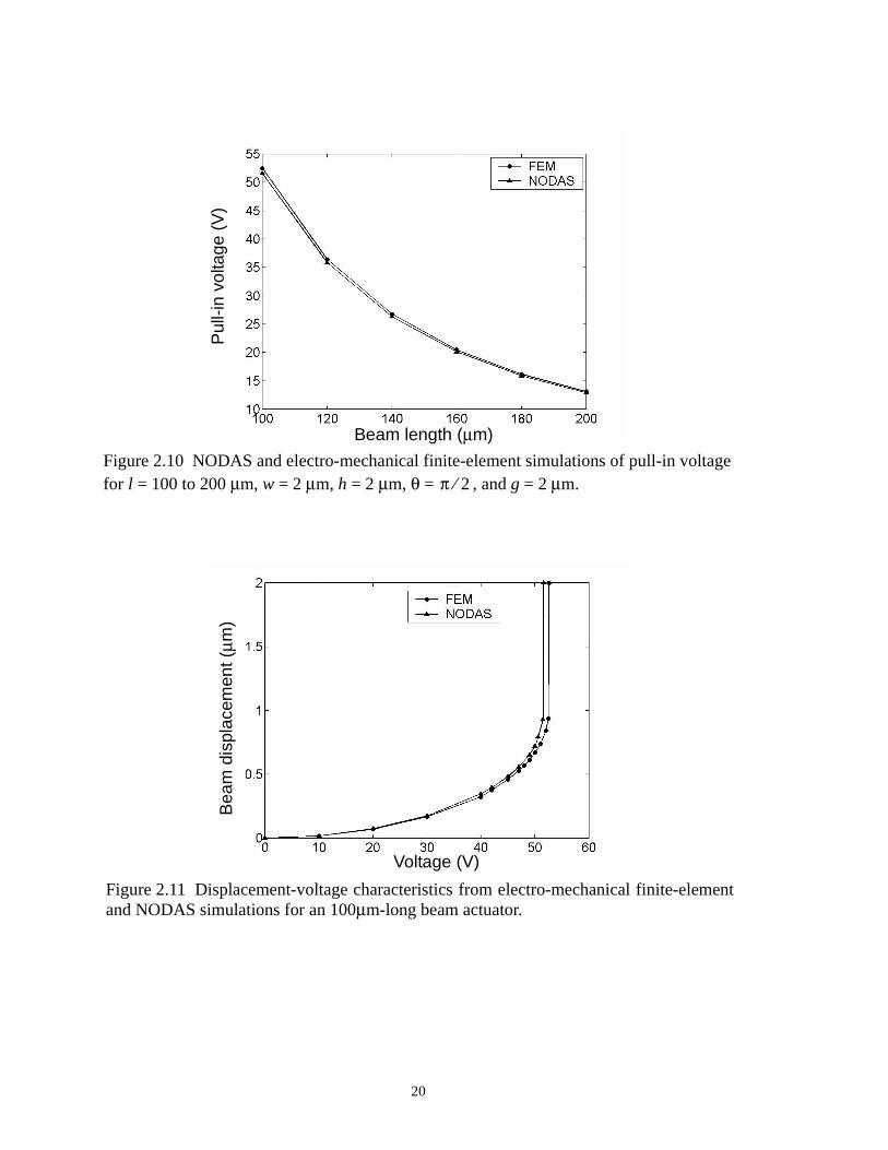
of the actuator as a function of beam length are plotted in Figure 2.10. A maximum of -
1.7% deviation of pull-in voltage from the finite element simulation is obtained by
NODAS simulations. Pull-in voltages in both simulations are inversely proportional to the
beam length squared.
Beam displacement of an 100 µm long beam with respect to the applied voltage
is illustrated in Figure 2.11. Good agreement is shown except near the edge of pull-in
point. For one data point, it takes NODAS simulation 1.7 seconds (CPU time) on the aver-
age to complete, compared to 280 seconds in electro-mechanical finite-element analysis.
π 2⁄
wl h
x
y
(a)z
Figure 2.9 Cantilever beam actuator. (a) Geometry from the top view, where l = 100 to200 µm, w = 2 µm, h = 2 µm, θ = , and g = 2 µm. (b) Schematic representation ofinterconnected beams and gaps for NODAS simulation.
π 2⁄
g
(b)
19
Pul
l-in
volta
ge (
V)
Beam length (µm)
Figure 2.10 NODAS and electro-mechanical finite-element simulations of pull-in voltagefor l = 100 to 200 µm, w = 2 µm, h = 2 µm, θ = , and g = 2 µm.π 2⁄
Voltage (V)
Bea
m d
ispl
acem
ent (
µm)
Figure 2.11 Displacement-voltage characteristics from electro-mechanical finite-elementand NODAS simulations for an 100µm-long beam actuator.
20

2.5 Experiment
Pull-in voltages of beam actuators fabricated by the polysilicon micromachining
process (MUMPs [35]) are measured and compared with NODAS and finite-element sim-
ulations as listed in Table 2.1. Actual beam cross-section and gap separation are taken into
account in both simulations (w = 1.7 µm, h = 2 µm, θ = 1.496 radians, and g = 2.3 µm);
otherwise up to 25% pull-in voltage deviation occurs with only nominal layout dimen-
sions considered.
l(µm)Experiment
(V)NODAS
(V)FEM (V)
100 40.0 42.5 (+6.3%)
44.2 (+10.5%)
150 18.4 19.1 (+3.8%)
19.7 (+7.1%)
200 10.4 11.0 (+5.8%)
11.1 (+6.7%)
Table 2.1: Measured pull-in voltage of polysilicon beam actuators compared with NODAS and electro-mechanical finite-element simulation results.
21

22

Chapter 3
Plant Design and Modeling
3.1 Introduction
In this chapter, we will present the design and modeling of the controlled plant
which consists of a micromechanical actuator driven by the parallel-plate electrostatic
force, followed by a capacitive position sensor. Electrostatic actuation and capacitive
sensing are used for their low power consumption which is ideal for the envisioned porta-
ble storage device. We begin with an introduction of device fabrication using CMOS-
MEMS technology, and material property characterization of the CMOS-MEMS micro-
structures. The design and modeling aspects of the actuator and capacitive sensing circuit
will be presented to establish a complete dynamic model of the plant for use in controller
design, which is the topic of the next chapter.
3.2 CMOS-MEMS Fabrication
The conventional CMOS process has been used for MEMS fabrication in many
ways, in which additional fabrication steps can be applied either before [46][47], in
between [48], or after [49-51] the regular CMOS process. Our goal to achieve low-cost
integration of micromechanical structures and high-performance electronics involves only
a minimum of processing steps on CMOS layers after the completed CMOS process,
thereby enabling a shift in research focus from processing details to the design of complex
systems with multiple sensors and actuators on a single chip.
23

Microactuators described in this thesis are fabricated in a conventional CMOS
processes followed by post-CMOS micromachining steps described in [52]. First, an
anisotropic dielectric reactive-ion etch (RIE) with CHF3/O2 plasma defines the structural
sidewalls using the top metal layer as an etch-resistant mask. Next, an anisotropic silicon
deep reactive-ion etch (DRIE) is performed in an inductively-coupled-plasma etcher using
SF6 (etching) and C4F8 (passivation) plasmas. Finally microstructures are released from
silicon substrate by an isotropic silicon etch with SF6 plasma. Fabricated composite
microstructures can consist of metal layers, dielectric layers, and polysilicon layers. A
complete post-processing sequence is illustrated in Figure 3.1. A released crab-leg comb-
drive resonator fabricated by the Agilent 0.5 µm three-metal n-well CMOS process is
shown in Figure 3.2(a). A released beam cross-section with three metal layers (metal-3,
metal-2, and metal-1) and one polysilicon layer is in Figure 3.2(b). When using dielectric
RIE for post-CMOS processing, one must consider the following factors: (1) It is desirable
to have high etch selectivity between the metal mask layer and dielectric layers (i.e., sili-
con dioxide and silicon nitride), and no selectivity between these dielectric layers in the
vertical etch direction. (2) It is desirable to achieve directivity of sidewalls by control of
passivation on sidewalls. However, too much polymerization on the surface will slow
down dielectric etch and limit the smallest etched gaps and holes; too little polymerization
does not provide enough sidewall protection, resulting in the loss of critical dimensions. A
beam cross-section with excessive polymers stacked on sidewalls is illustrated in Figure
3.3. (3) It is essential to avoid electrical connection failure during etch. Failures can result
from the removal of metal layers on vias connecting to the top metal layer, as shown in
24

Figure 3.1 Cross section of the CMOS-MEMS process flow. (a) After CMOS process-ing. (b) After anisotropic dielectric reactive-ion etch for definition of structural side-walls. (c) After anisotropic silicon etch. (d) After isotropic silicon etch for structuralrelease.
metallization layers
dielectric layers
gate polysiliconpolysilicon
silicon substrate
CMOS regionmicrostructural region
(a)
(b)
(c)
(d)
25

Figure 3.4(a), and from lateral etching of refractory titanium/tungsten layers deposited on
the top and bottom of aluminum layers in the sub-micron CMOS process, as shown in Fig-
ure 3.4(b).
To summarize, the important etch effects include etch rate, loss of critical dimen-
sions, survival of electrical connection, and polymer generated on the sidewall and in the
field. The processing parameters in the plasma system which affect the RIE etch include
gas flow rate, gas mixture, pressure, RF power, electrode spacing, electrode temperature,
Figure 3.2 (a) Fabricated crab-leg comb-drive resonator using the Agilent 0.5 µmthree-metal n-well process. (b) Beam cross-section with three metal layers, inter-metaldielectric layers, and polysilicon.
metal-3
metal-2
polysilicon
metal-1
silicon substrate
comb-drives
crab-legflexures
Figure 3.3 Polymers stacked on beam sidewalls resulted from excessive polymerizationduring dielectric RIE.
polymer
beam
26

electrode material, total wafer area (loading), and previous processing steps. Three critical
processing parameters (pressure, power, and mixture of gases) are selected to quantify the
process model in a Box-Behnken factorial experiment [53] reported by Zhu [54]. The
CHF3/O2 gas mixture is chosen instead of the CF4/O2 mixture used previously in [52]
because it can generate sufficient passivation with a reasonable etch rate and with fewer
electrical connection failures. The dielectric RIE is performed in a Plasma-Therm 790
reactor. The processing region for achieving minimal lateral etch, minimum polymeriza-
tion, and electrical continuity of vias is determined, resulting in the process parameters:
125 mTorr chamber pressure, 0.55 W/cm2 RF power density, CHF3 flow at 22.5 sccm,
and O2 flow at 16 sccm. Experimental results summarized in [54] indicate: (1) Etch rate
increases with increasing RF power and chamber pressure, and is not significantly
affected by O2 concentration. (2) Increasing RF power and decreasing pressure reduce
passivation. (3) High-power operation must be accompanied by increasing chamber pres-
sure to reduce the loss of critical dimensions and opened vias resulting from the ion-mill-
Figure 3.4 Failure mechanisms of electrical connections: (a) opened vias, and (b) lateraletch of refractory Ti/W layers deposited on top and bottom of metal layers.
etched Ti/Wopened vias
27

ing effect. At an etch rate of 425 Å/min, it takes about two hours to etch through all the
dielectric layers (~5 µm thick).
The previous processing procedure described in [52] does not have the anisotro-
pic silicon DRIE step inserted between the dielectric RIE and the isotropic release etch.
Microstructural release is performed directly after dielectric RIE. The drawback is that the
vertical etch and the lateral etch are coupled in an isotropic etch, hence the circuitry must
be placed at least about as far as the silicon is etched down. The primary benefit of using
the anisotropic silicon DRIE is that the vertical etch and the lateral etch are decoupled.
Separation between the sensing device and silicon substrate is wider than achieved in [52],
therefore parasitic capacitances can be reduced. The amount of the required lateral etch for
structural release is also reduced depending on designed dimensions. The anisotropic sili-
con DRIE is performed in a Surface Technology Systems (STS) inductively-coupled-
plasma (ICP) etcher. The process parameters for the etch part include 600 W coil power,
12 W platen power, SF6 flow at 130 sccm, O2 flow at 20 sccm, and 23 mTorr chamber
pressure. The fluorocarbon polymer passivation cycle is performed using 600 W coil
power, C4H8 flow at 85 sccm, 12 mTorr chamber pressure, and no platen power. The
duration of the etching and passivation cycles are 12 seconds and 8 seconds, respectively,
with achieved etch rate of 2.9 µm/min.
The isotropic silicon etch is also performed in the STS ICP etcher, because there
is no noticeable decrement of aluminum layer thickness, as observed commonly in the
parallel-plate system (e.g., Plasma-Therm 790 etcher). A Box-Behnken factorial experi-
ment [53] has been performed with three major processing parameters: pressure, platen
power, and SF6 flow. The experimental results [55] show that the etch rate is primarily
28

determined by the pressure, followed by SF6 flow, and not significantly affected by platen
power especially under high pressure. The processing parameters are: 600 W coil power,
50 mTorr chamber pressure, SF6 flow at 50 sccm, and no platen power.
3.3 Material Property Characterization
In this section, measured material properties of CMOS-MEMS microstructures
are presented. Devices are fabricated by the Agilent 0.5 µm CMOS process available
through the MOS Implementation Service (MOSIS). Reported material properties include
effective Young’s modulus in the lateral direction, residual stress and vertical stress gradi-
ent [56] measured on dice from the same run, and dice from different runs as well. A dura-
bility test is performed on a resonating fatigue structure to demonstrate the effect of cyclic
stress on composite micromechanical structures.
3.3.1 Effective Young’s Modulus
Effective Young’s modulus is determined by measuring the lateral resonant fre-
quency of simple cantilever-beam actuators shown in Figure 3.5. Beams are excited elec-
Figure 3.5 Resonant beam actuators for measuring effective Young’s modulus of com-posite beams.
electrostatic actuator
cantilever beam
29

trostatically by the actuators located near the tips of the cantilevers. The measured
frequencies are substituted into the analytic equation for resonance frequency of a homo-
geneous cantilever beam [57],
(3.1)
where L is the beam length, E is the effective Young’s modulus, I is the moment of inertia
of the beam cross-section, ρ is the effective mass density, A is the beam cross-section area,
and the unit of frequency in Hertz. The effective mass density of composite beams is the
average density of constituent materials given by,
(3.2)
where ρAl, ρox, and ρpoly are the mass density of bulk aluminum, silicon dioxide, and pol-
ysilicon with values of 2700 kg/m3, 2500 kg/m3, and 2330 kg/m3, respectively. AAl, Aox,
and Apoly are the cross-section areas occupied by aluminum, silicon dioxide and polysili-
con.
Composite beams with fourteen combinations of metal and polysilicon layers are
measured. Each cantilever is designed 2.1 µm wide and 90 µm long in layout. The actual
dimensions of beam cross-sections are measured from scanning electron micrographs to
calculate the moment of inertia and the effective mass density. Table 3.1 summarizes the
effective Young’s modulus measured on three dice from the MOSIS N78H-AV run of Agi-
lent 0.5 µm CMOS. The volume ratio of dielectric to metal in the right column illustrates
that effective Young’s modulus tends to increase when structures contain more dielectric
than metal. Another measurement of five commonly used composite beams on three dice
fr 0.56 EI
ρAL4
-------------=
ρρAlAAl ρoxAox ρpolyApoly+ +( )
A---------------------------------------------------------------------------=
30

from the MOSIS N6CJ-AY run are tabulated in Table 3.2, with previous results from the
N78H-AV run for comparison. Both die-to-die and run-to-run variation of Young’s modu-
lus are within ±8%, and within ±3% for m3-m2-m1-poly beams.
3.3.2 Residual Stress and Vertical Stress Gradient
Residual stress is measured using the bent-beam strain sensor [58] shown in Fig-
ure 3.6(a). Relative apex displacement of the bent-beam rendered by the residual stress is
read out from a vernier. Residual stress of seven composite test structures was analyzed by
m3 m2 m1 poly die no.1 die no.2 die no.3 averagestandard deviation
volume(dielectric:
metal)
• • • • 63 ± 0.4 62 ± 0.4 61 ± 0.4 62.0 0.82 4.02 : 1• • • 64 ± 0.4 62 ± 0.4 60 ± 0.4 62.0 1.63 4.15 : 1• • • 73 ± 0.4 69 ± 0.4 67 ± 0.4 69.7 2.49 5.77 : 1• • 73 ± 0.4 71 ± 0.4 67 ± 0.4 70.3 2.49 5.95 : 1• • • 73 ± 0.4 71 ± 0.4 66 ± 0.4 70.3 2.94 5.77 : 1• • 74 ± 0.4 71 ± 0.4 69 ± 0.4 71.3 2.05 5.95 : 1• • 82 ± 0.4 80 ± 0.4 75 ± 0.4 79.0 2.94 9.39 : 1• 83 ± 0.4 80 ± 0.4 77 ± 0.4 80.0 2.45 9.67 : 1
• • • 67 ± 0.3 N/A 65 ± 0.3 66.0 1.00 5.28 : 1• • 67 ± 0.3 66 ± 0.3 N/A 66.5 0.50 5.50 : 1• • 78 ±0.3 75 ± 0.3 75 ± 0.3 76.0 1.41 10.10 : 1• 77 ± 0.3 78 ± 0.3 79 ± 0.3 78.0 0.82 10.50 : 1
• • N/A 66 ± 0.3 67 ± 0.3 66.5 0.50 4.92 : 1• N/A 67 ± 0.3 67 ± 0.3 67.0 0.00 5.35 : 1
Table 3.1 Measured effective Young’s modulus (in GPa) of composite beams fromMOSIS N78H-AV run.
beam type
m3 m2 m1 poly
N6CJ-AYN78H-AVAveragedie no.1 die no.2 die no.3 Average
standard deviation
• • • • 65 ± 0.5 63 ± 0.5 62 ± 0.5 63.3 1.25 62.0• • • 66 ± 0.5 65 ± 0.5 64 ± 0.5 65.0 0.82 62.0• • 74 ± 0.5 70 ± 0.5 70 ± 0.5 71.3 1.89 70.3• • 75 ± 0.5 71 ± 0.5 71 ± 0.5 72.3 2.16 71.3• 89 ± 0.4 88 ± 0.4 91 ± 0.4 89.3 1.25 80.0
beam type
Table 3.2 Measured effective Young’s modulus (in GPa) of composite beams fromN6CJ-AV run and comparison with average values of N78H-AV run.
31
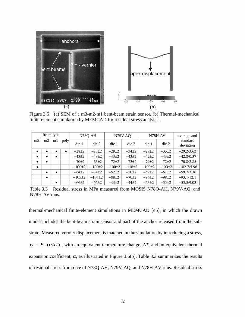
thermal-mechanical finite-element simulations in MEMCAD [45], in which the drawn
model includes the bent-beam strain sensor and part of the anchor released from the sub-
strate. Measured vernier displacement is matched in the simulation by introducing a stress,
, with an equivalent temperature change, ∆T, and an equivalent thermal
expansion coefficient, α, as illustrated in Figure 3.6(b). Table 3.3 summarizes the results
of residual stress from dice of N78Q-AH, N79V-AQ, and N78H-AV runs. Residual stress
vernierbent beams
anchors
Figure 3.6 (a) SEM of a m3-m2-m1 bent-beam strain sensor. (b) Thermal-mechanicalfinite-element simulation by MEMCAD for residual stress analysis.
apex displacement
(a) (b)
σ E α∆T( )⋅=
m3 m2 m1 polyN78Q-AH N79V-AQ N78H-AV average and
standard deviation die 1 die 2 die 1 die 2 die 1 die 2
• • • • −28±2 −23±2 −28±2 −34±2 −29±2 −33±2 −29.2/3.62• • • −43±2 −43±2 −43±2 −43±2 −42±2 −43±2 −42.8/0.37• • −70±2 −65±2 −72±2 −72±2 −74±2 −72±2 −70.8/2.85• −100±2 −100±2 −100±2 −116±2 −100±2 −100±2 −102.7/5.96
• • −64±2 −74±2 −52±2 −50±2 −59±2 −61±2 −59.7/7.36• −105±2 −105±2 −88±2 −70±2 −96±2 −98±2 −93.1/12.1
• −66±2 −66±2 −44±2 −44±2 −53±2 −53±2 −53.3/9.03
Table 3.3 Residual stress in MPa measured from MOSIS N78Q-AH, N79V-AQ, andN78H-AV runs.
beam type
32

tends to increase when structures have more dielectric content. Beams containing all four
conductors have relatively low compressive stress around 29.2 MPa with a 20% variation.
Curling of the structural material arises from the vertical stress gradient in the
composite structures. Measured beam curl in a localized area as shown in Figure 3.7 dis-
plays much less variation than measured curl from different dice. Table 3.4 summarizes
the measured out-of-plane radius of curvature of various 100 µm long, 2.1 µm wide com-
posite beams from dice of N78Q-AH, N79V-AQ, and N78H-AV runs. Beams using
metal-3 as the top layer display less curl than those using metal-2 or metal-1 as the top
layer. Equations for predicting curl of multi-morph structures have been derived based on
the parameter extraction technique [59].
3.3.3 Cyclic Fatigue
Cyclic fatigue of the CMOS microstructures is investigated using a modified
fatigue structure [60] shown in Figure 3.8(a). Stress concentration induced by cyclic
metal-3 beams
metal-1-3 beams
Figure 3.7 Uniform curl of local metal-3 and metal-1-3 beams.
33
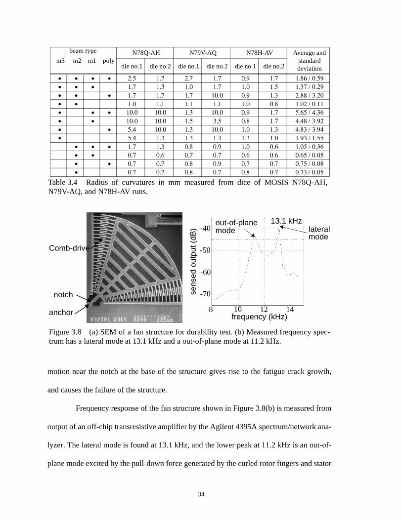
motion near the notch at the base of the structure gives rise to the fatigue crack growth,
and causes the failure of the structure.
Frequency response of the fan structure shown in Figure 3.8(b) is measured from
output of an off-chip transresistive amplifier by the Agilent 4395A spectrum/network ana-
lyzer. The lateral mode is found at 13.1 kHz, and the lower peak at 11.2 kHz is an out-of-
plane mode excited by the pull-down force generated by the curled rotor fingers and stator
m3 m2 m1 polyN78Q-AH N79V-AQ N78H-AV Average and
standard deviation die no.1 die no.2 die no.1 die no.2 die no.1 die no.2
• • • • 2.5 1.7 2.7 1.7 0.9 1.7 1.86 / 0.59• • • 1.7 1.3 1.0 1.7 1.0 1.5 1.37 / 0.29• • • 1.7 1.7 1.7 10.0 0.9 1.3 2.88 / 3.20• • 1.0 1.1 1.1 1.1 1.0 0.8 1.02 / 0.11• • • 10.0 10.0 1.3 10.0 0.9 1.7 5.65 / 4.36• • 10.0 10.0 1.5 3.5 0.8 1.7 4.48 / 3.92• • 5.4 10.0 1.3 10.0 1.0 1.3 4.83 / 3.94• 5.4 1.3 1.3 1.3 1.3 1.0 1.93 / 1.55
• • • 1.7 1.3 0.8 0.9 1.0 0.6 1.05 / 0.36• • 0.7 0.6 0.7 0.7 0.6 0.6 0.65 / 0.05• • 0.7 0.7 0.8 0.9 0.7 0.7 0.75 / 0.08• 0.7 0.7 0.8 0.7 0.8 0.7 0.73 / 0.05
Table 3.4 Radius of curvatures in mm measured from dice of MOSIS N78Q-AH,N79V-AQ, and N78H-AV runs.
beam type
13.1 kHzout-of-planemode lateral
mode
frequency (kHz)
sens
ed o
utpu
t (dB
) -40
-50
-60
-70
10 12 148anchor
notch
Comb-drive
Figure 3.8 (a) SEM of a fan structure for durability test. (b) Measured frequency spec-trum has a lateral mode at 13.1 kHz and a out-of-plane mode at 11.2 kHz.
34

fingers. A durability test is performed with an a.c. driving voltage of 40 V amplitude
biased at 55 V d.c., producing a maximum deflection of 10 ± 1 µm measured at the free
end of the structure. Failure of the notch is observed after 72 minutes for over 45 million
experienced cycles. Figure 3.9(a) shows the change in resonance frequency with respect to
the experienced cycles. Scanning electron micrographs of the notch taken before and after
the test are shown in Figure 3.9(b) and Figure 3.9(c). The maximum stress value near the
notch is 620 ± 60 MPa by finite element analysis.
3.4 Parallel-Plate Microactuator Design
3.4.1 Dynamic Equation
A conventional parallel-plate electrostatic actuator shown schematically in Fig-
ure 3.10 is represented by a lumped-parameter model using mass, damper, and mechanical
spring elements. Using the free-body diagram in Figure 3.10(b) and the Newton’s second
law, we obtain the balanced force equation,
Figure 3.9 (a) Resonant frequency change of the fatigue structure with respect to theexperienced cycles. (b) Side view of the notch before testing. (c) Broken notch after test-ing.
(a) (b) (c)107 cyclesre
sona
nt fr
eque
ncy
(kH
z)
35
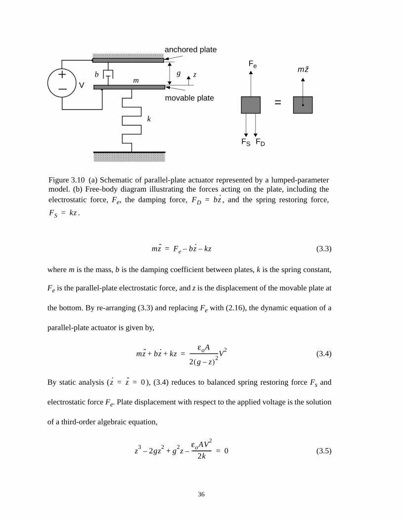
(3.3)
where m is the mass, b is the damping coefficient between plates, k is the spring constant,
Fe is the parallel-plate electrostatic force, and z is the displacement of the movable plate at
the bottom. By re-arranging (3.3) and replacing Fe with (2.16), the dynamic equation of a
parallel-plate actuator is given by,
(3.4)
By static analysis ( ), (3.4) reduces to balanced spring restoring force Fs and
electrostatic force Fe. Plate displacement with respect to the applied voltage is the solution
of a third-order algebraic equation,
(3.5)
+_g z
V
k
bm
Figure 3.10 (a) Schematic of parallel-plate actuator represented by a lumped-parametermodel. (b) Free-body diagram illustrating the forces acting on the plate, including theelectrostatic force, Fe, the damping force, , and the spring restoring force,
.
FD bz·=
FS kz=
anchored plate
movable plate
FDFS
Fe
= •
mz··
mz·· Fe bz·– kz–=
mz·· bz· kz+ +εoA
2 g z–( )2----------------------V
2=
z· z·· 0= =
z3
2gz2
– g2z
εoAV2
2k---------------–+ 0=
36

(3.5) suggests that parallel-plate actuators have multiple equilibrium points at a given volt-
age. To determine the convergence of these equilibrium points, we compare the force gra-
dients of spring-restoring force and electrostatic force given by,
(3.6)
and
(3.7)
at an equilibrium point z = Zo. Zo is a stable equilibrium point when the value of (3.6) is
larger than that of (3.7), and is an unstable equilibrium point otherwise. The actuator is
marginally stable at displacement of one-third of the gap known as the electrostatic pull-in
limit. The pull-in voltage, Vpi, corresponding to the pull-in point, is the maximum applied
voltage for stable open-loop operation obtained by solving (3.5) with z = g/3,
(3.8)
A typical displacement-voltage curve of a parallel-plate actuator is in Figure 3.11, illus-
trating two equilibrium points at each voltage except at V = Vpi.
3.4.2 Design Description
As introduced in Chapter 1, each magnetic probe tip actuator is servoed indepen-
dently to complete the reading and writing actions. The actuator design for the envisioned
system implementation must consider the following factors:
Fsd zd⁄ k=
εoA
2z g z–( )2------------------------V
2=
Fe∂ z∂⁄εoA
g z–( )3------------------V
2=
Vpi8kg3
27εoA---------------=
37
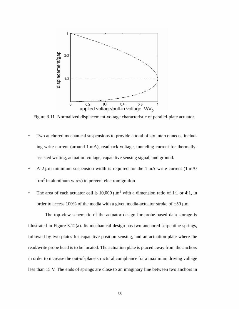
• Two anchored mechanical suspensions to provide a total of six interconnects, includ-
ing write current (around 1 mA), readback voltage, tunneling current for thermally-
assisted writing, actuation voltage, capacitive sensing signal, and ground.
• A 2 µm minimum suspension width is required for the 1 mA write current (1 mA/
µm2 in aluminum wires) to prevent electromigration.
• The area of each actuator cell is 10,000 µm2 with a dimension ratio of 1:1 or 4:1, in
order to access 100% of the media with a given media-actuator stroke of ±50 µm.
The top-view schematic of the actuator design for probe-based data storage is
illustrated in Figure 3.12(a). Its mechanical design has two anchored serpentine springs,
followed by two plates for capacitive position sensing, and an actuation plate where the
read/write probe head is to be located. The actuation plate is placed away from the anchors
in order to increase the out-of-plane structural compliance for a maximum driving voltage
less than 15 V. The ends of springs are close to an imaginary line between two anchors in
Figure 3.11 Normalized displacement-voltage characteristic of parallel-plate actuator.
applied voltage/pull-in voltage, V/Vpi
1/3
2/3
1
disp
lace
men
t/gap
38

Figure 3.12 (a) Schematic of tip actuator design for probe-based data storage. (b) to (f):Side view at cross-section lines, illustrating electrical connections using three metal lay-ers.
sensing plates
actuation plate
springs
anchors
aa’ bb’
GND
actuation
GND
actuation
senseGND
sense
a a’ b b’ c c’
GNDsense
(a)
(b) (c) (d)
(e)
c’ d’
c de
e’
GNDd d’
e e’(f)
actuationsense
d.c.-ground bar
x
y
z
39

order to reduce the structural curl close to the anchor level as the springs fold back,
thereby decreasing the eventual curl of actuation plate as shown in the side-view sche-
matic of curl design in Figure 3.13(a). An alternate design with springs ending away from
the anchors has more actuation-plate curl and out-of-plane initial displacement as shown
in Figure 3.13(b). To ensure final structural release, the plates are separated to provide suf-
ficient silicon undercut. From another perspective, the separation of the actuation and the
sensing plates is also required to reduce signal feedthrough.
An external planar electrode will be placed on top of the actuator (not shown in
Figure 3.12(a)) to form the actuated and sensing capacitances. A total of three electrical
connections are required for parallel-plate servo: z actuation, capacitive sensing, and
ground. The current design is for test of position servo only. Wires for read, write, and tun-
neling current can be considered as a.c. ground. Therefore they are d.c. grounded during
the servo test. Actuation and sensing signals are carried by metal-1 through the left and
right springs individually to the desired plates in order to reduce signal feedthrough, as
shown in cross-section view in Figure 3.12(b), (c), (e), and (f). The metal-3 on top of the
springs is d.c. grounded, producing nearly zero electrostatic force with respect to the top
curlcurl
spring beamssensing plates
anchor
(a) (b)Figure 3.13 Side view schematic of actuator curl design. (a) Ends of springs are close toa straight line between anchors in design. (b) Ends of springs are away from anchors indesign.
actuation plates spring beams sensing plates
actuation plates
anchor
40

electrode. A metal-3 cut is needed between the springs and the sensing plate, and between
the sensing and actuation plates for separation of signals and ground, as shown in Figure
3.12(d), (e), and (f). A d.c.-ground shield provided by metal-2 is inserted between over-
lapped actuation and sensed wires to reduce signal feedthrough, as shown in Figure
3.12(d) and (e). Similarly a d.c.-ground mechanical bar between actuation and sensing
plates, as shown in Figure 3.12(a) and (f), is designed to shunt field lines between plates
for feedthrough reduction.
3.4.3 Spring Constant
In this section, the energy method (Castigliano’s second theorem) is used to
derive an analytic formula for actuator spring constant in the out-of-plane direction. A
comprehensive spring-constant analysis of four flexures that are commonly used in micro-
mechanical designs is found in [61]. A schematic of the actuator design is re-drawn in Fig-
ure 3.14. Each meander in the spring consists of a connector beam of length a and width
wa, and a span beam of length b and width wb. The last beam of the spring measures length
c and width wc, and each plate is of size w × l. The distance between two meandering
springs is d. ly is the distance defined from center of the actuation plate to the end of
spring. l0, l1, and l2 are the distances measured from the top of the spring to the center of
the actuation plate, sensing plate 1, and sensing plate 2. The beams between plates are of
length ld and width wd. h is the beam thickness pointed into the z direction. The goal is to
find the displacement resulting from a lumped electrostatic force applied at the center of
the actuation plate. The spring constant is defined as the ratio of force over displacement.
41
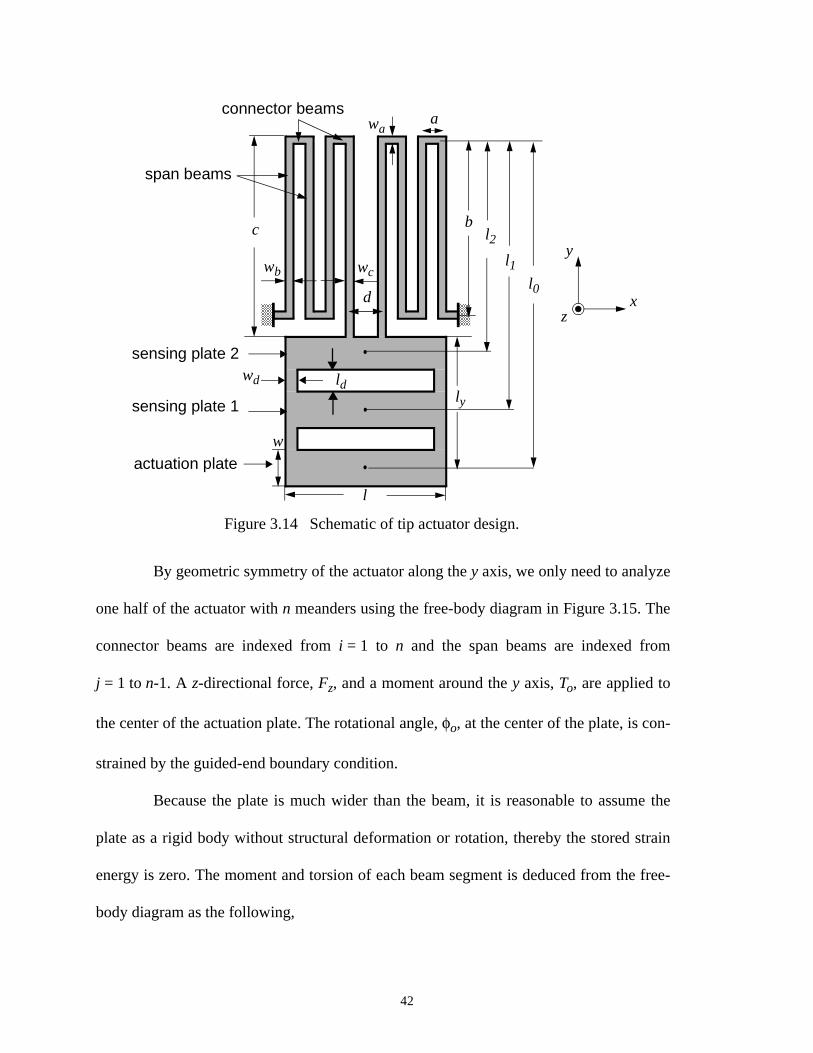
By geometric symmetry of the actuator along the y axis, we only need to analyze
one half of the actuator with n meanders using the free-body diagram in Figure 3.15. The
connector beams are indexed from i = 1 to n and the span beams are indexed from
j = 1 to n-1. A z-directional force, Fz, and a moment around the y axis, To, are applied to
the center of the actuation plate. The rotational angle, φo, at the center of the plate, is con-
strained by the guided-end boundary condition.
Because the plate is much wider than the beam, it is reasonable to assume the
plate as a rigid body without structural deformation or rotation, thereby the stored strain
energy is zero. The moment and torsion of each beam segment is deduced from the free-
body diagram as the following,
Figure 3.14 Schematic of tip actuator design.
span beams
b
a
l
w
ly
connector beams
c
x
y
zd
wd
wa
l2
l1l0
actuation plate
sensing plate 1
sensing plate 2
wcwb
ld
42

Fz
To
Tp
Mp Fz
Tp
Fz Mp
Tp
Fz Mc
Tp
Mc
FzFz
Ti1
Mc
x
x
i = 1
Ti1
Fz Mc
Fz
x
Tj1
Ti1
j = 1
FzFz
Ti2x
i = 2
Tj1
Ti1
Tj1
Ti2
Fz
Fz
x
Tj1
Ti2
Tj2
j = 2
FzFz
Ti3x
Tj2
Ti2
Tj2
i = 2
Ti(n-1)
Fz Tj(n-1)
Fz
x
Tjn
Ti(n-1)
j = n - 1
Fz
xTjn
Ti(n-1)
Figure 3.15 Free-body diagram of one half of actuator used for deriving z-directionalspring constant.
φo
d/2
43
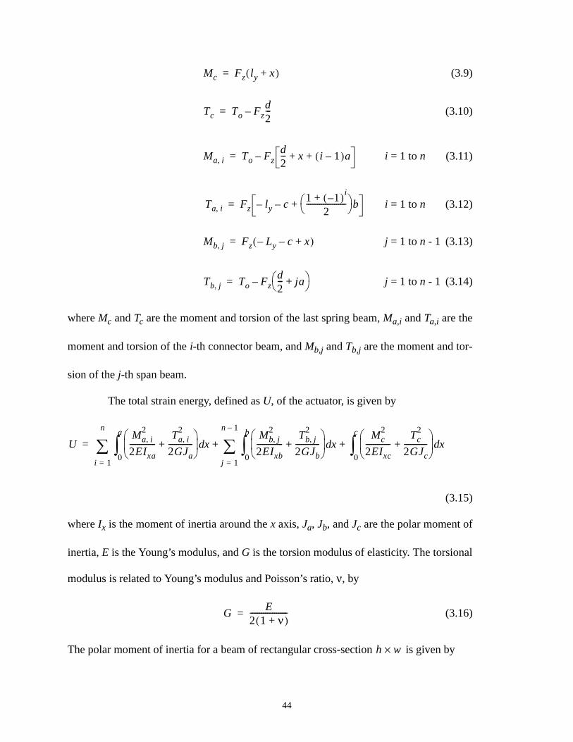
(3.9)
(3.10)
i = 1 to n (3.11)
i = 1 to n (3.12)
j = 1 to n - 1 (3.13)
j = 1 to n - 1 (3.14)
where Mc and Tc are the moment and torsion of the last spring beam, Ma,i and Ta,i are the
moment and torsion of the i-th connector beam, and Mb,j and Tb,j are the moment and tor-
sion of the j-th span beam.
The total strain energy, defined as U, of the actuator, is given by
(3.15)
where Ix is the moment of inertia around the x axis, Ja, Jb, and Jc are the polar moment of
inertia, E is the Young’s modulus, and G is the torsion modulus of elasticity. The torsional
modulus is related to Young’s modulus and Poisson’s ratio, ν, by
(3.16)
The polar moment of inertia for a beam of rectangular cross-section is given by
Mc Fz ly x+( )=
Tc To Fzd2---–=
Ma i, To Fzd2--- x i 1–( )a+ +–=
Ta i, Fz ly– c–1 1–( )i
+2
--------------------- b+=
Mb j, Fz Ly– c– x+( )=
Tb j, To Fzd2--- ja+ –=
UMa i,
2
2EIxa--------------
Ta i,2
2GJa-------------+
xMb j,
2
2EIxb--------------
Tb j,2
2GJb-------------+
xMc
2
2EIxc-------------
Tc2
2GJc------------+
xd0
c
∫+d0
b
∫j 1=
n 1–
∑+d0
a
∫i 1=
n
∑=
GE
2 1 ν+( )--------------------=
h w×
44

(3.17)
where .
The actuator displacement z is found by solving the two simultaneous equations:
(3.18)
(3.19)
The z-directed actuator spring constant is kz = 2Fz/z. We assume that Ixb = Ixc and Jb = Jc.
For n is always even in our design, the spring constant is given by,
(3.20)
where , , , and .
(3.20) is further reduced assuming that all the beam cross-sections are the same
(Ixa = Ixb = Ixc and Ja = Jb =Jc), giving,
J13---h
3w 1
192π5
--------- hw---- 1
n5----- nπw
2h----------- tanh
n 1 odd,=
∞
∑–
=
h w<
φoU∂To∂
-------- 0= =
zU∂Fz∂
--------=
kz
24SaSbGaGb cSa b n 1–( )Sa naGb+ +( )
4Sa2GaGb c b n 1–( )+( ) c( c
23cly 3ly
2+ +( ) b
3n 1–( ) 3b
2ly n 1–( ) 3b
2+ + +
ly2
n 1–( ) ) 2aSaGb 2c c2GaGb 3cGaGbly 3 SaSb GaGb+( )ly
2 ) 6bly–+ +(–[–
cSaSb n 1–( ) SaSb GaGb+( )ly+( ) 3b2
n 1–( ) cSaSb 2 SaSb GaGb+( )ly+( )–
b–3
3SaSb 2GaGb+( ) n 1–( ) ]n a4SbGaGb
2n
42a
3SaSbGaGbn
2b n 1–( )2(+ +
2cn ) a2SaSbn 12Gb
2ly2n b
2SaGa n 2–( ) n 1–( )2
6Gb2n ) 2b 6Gb
2(+ +(+[+ +
lyn cSaGa 1 3n– 2n2
+( ) ) ]+ -------------------------------------------------------------------------------------------------------------------------------------------------------------------------------------------------=
Sa EIxa≡ Sb EIxb≡ Ga GJa≡ Gb GJb≡
45

(3.21)
Analytic spring constants and finite-element simulations are compared using the
following design parameters: E = 70 GPa, a = 4 µm, b = 108 µm, c = 113 µm,
d = 15.5 µm, wa = wb = wc = 2 µm, wd = 5 µm, ld = 10 µm, w = 20 µm, l = 80 µm,
ly = 70 µm, and h = 4.5 µm. The number of connectors n in each spring is even-numbered
from 2 to 8 (n = 6 for the final design). The finite-element analysis and analytic calcula-
tions match to better than 0.33% for all cases as shown in Figure 3.16. The designed actu-
ator has a spring constant kz = 0.167 N/m.
kz
24SaGa bSa aGa+( )
n
4b2SaGa b
23bly 3ly
2+ +( ) 2ab b
23Sa
22Ga
2+( ) 6b Sa
2Ga
2+( )ly
2+ +[+
6 Sa2
Ga2
+( )ly2 ] a
4Ga
2n
22a
3bSaGa 1 n
2+( ) a
2Sa 12bGaly +[+ + +
12Galy2
b2
6Ga Sa n2
1–( )+( ) ]+
-----------------------------------------------------------------------------------------------------------------------------------------------------------------------------------=
Figure 3.16 Comparison of analytic z-directional spring constants with finite-elementanalysis.
number of connector beams
% E
rror
46

3.4.4 Modal Analysis
In this section, an analytical finite-element method [62][63] is utilized for the z-
directional modal analysis of the continuous elastic microactuator. The result is expressed
as an implicit solution of the formulated eigenvalue problem which can be conveniently
solved by a computer program (MATLAB [64]), rather than an explicit analytical for-
mula. Even so, the advantage of this method is that it takes much less computing time than
the numerical finite-element method when many design iterations are needed, and gives
satisfactory results comparable to the numerical finite-element method.
In the actuator design, each plate occupies a relatively small portion of the total
area, resulting in high-order mechanical modes from the plate itself at very high frequen-
cies. These modes can be neglected for elementary modal analysis. It is reasonable to rep-
resent plates with beam elements in analysis without resorting to a more complicated plate
element, while having sufficient accuracy. By using interconnected beam elements with
multiple degrees of freedom, the equation of motion of the actuator is formulated as,
(3.22)
where [m] is the mass matrix, [k] is the stiffness matrix, is the vector of nodal dis-
placements and rotations, is the vector of accelerations, and F is the vector of exter-
nal forces and moments. For the case of free vibration with natural frequency ω, (3.22)
takes the following form:
(3.23)
which is suited for eigenvalue solutions.
m[ ] q·· k[ ] q + F =
q
q··
0 k[ ] ω2 m[ ]–[ ] q =
47

The beam element shown schematically in Figure 3.17 is used for the finite-ele-
ment analysis, and is capable of resisting axial forces (Fxa and Fxb), shearing forces (Fya,
Fyb, Fza, and Fzb), bending moments (Mya, Mza, Myb, and Mzb), and twisting torques (Mxa
and Mxb), allowing six degree-of-freedom motion (x, y, and z in translation. θ, φ, and ϕ in
rotation) at nodes a and b. The stiffness and mass matrices of the beam element are
obtained by substituting the beam displacement functions into the kinetic energy expres-
sion and the strain energy expression, and performing the differentiations in the
Lagrange’s equation with respect to each degree-of-freedom [62]. For derivation of the z-
directional mode, the vector q can be reduced to q = za, θa, φa, zb, θb, φb, leading to
the stiffness and mass matrices given by,
x
z
y
Fxa
Fxb
Fya
Fyb
Fzb
FzaMxa
Mya
Mza
Mzb
MxbMyb
neutral axisθφ
ϕ
b
a
Figure 3.17 Twelve-degree-of-freedom beam finite element.
48

(3.24)
(3.25)
where ρ is the mass density, l is the beam length, A is the beam cross-section, and Jp is the
polar moment of inertia.
The force and moments acting on local coordinate axes of each beam element are
transformed to the global coordinate axes used by the actuator as shown in Figure 3.18.
Bars are added to all the symbols with reference to the local coordinate, which is oriented
k[ ]
12EIy
l3
--------------
0GJp
l--------- symmetrical
6EIy–l2
--------------- 04EIy
l-----------
12– EIy
l3----------------- 0
6EIy
l2-----------
12EIy
l3--------------
0GJp–
l------------- 0 0
GJp
l---------
6EIy–
l2-------------- 0
2EIy
l-----------
6EIy
l2----------- 0
4EIy
l-----------
=
m[ ] ρAl
1335------
0Jp
3A------- symmetrical
11l–210----------- 0
l2
105---------
970------ 0
13l–420----------- 13
35------
0Jp
6A------- 0 0
Jp
3A-------
13l420--------- 0
l2–140--------- 11l
210--------- 0
l2
105---------
=
49

at an angle measured counterclockwise from the global x axis. The resulting stiffness
and mass matrices transformed from the local matrices are given by,
(3.26)
(3.27)
where T is the transformation matrix given by,
Fz1
Fz2
Mx1
Mx2
My1
My2
Fz1
Fz2
Mx1
My1
My2Mx2
Φ
Φ
Figure 3.18 Transformation of a beam element from local to global (x, y) coordi-nates.
x y,( )
x
yxy
Φ
z z,
Φ
k[ ] T[ ]T k[ ] T[ ]=
m[ ] T[ ]T m[ ] T[ ]=
50

(3.28)
For the z-directional modal analysis, only half of the actuator is considered
because of its symmetry with respect to the y axis as shown in Figure 3.19. Starting from
the connector at the left, a total of (2n + 5) beam elements and (2n + 6) nodes are num-
bered in a continuous sequence, with n as the total number of connectors in one half of the
actuator. By tracing along the beam elements in ascending node number, the orientation of
each beam element is found at 0° for all connectors, 90° for span beams pointed toward
T[ ]
1 0 0 0 0 0
0 Φcos Φsin 0 0 0
0 Φsin– Φcos 0 0 0
0 0 0 1 0 0
0 0 0 0 Φcos Φsin
0 0 0 0 Φsin– Φcos
=
Figure 3.19 Schematic of one half of the actuator represented by beam elements forfinite-element modal analysis. Nodes are numbered from 1 to 2n + 6, with n representingthe number of connector beams.
b
a
l/2
w
c
x
y
z
••••
1 2
3 4 2n2n-1
2n+1
2n+2
2n+3
2n+4
2n+5
2n+6
•
• •
•
•
• •
•
•
•
•
•
•
5 6
wdld
wb
wa
wc
51
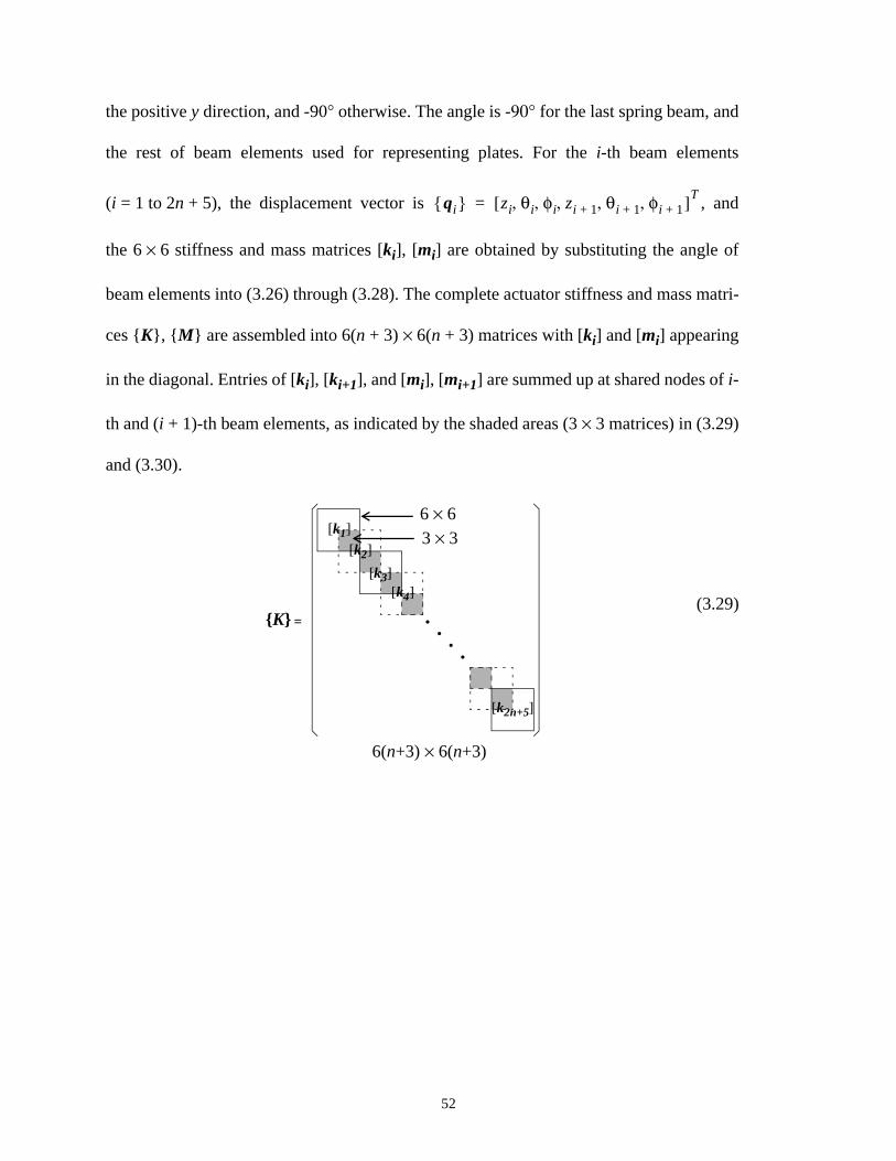
the positive y direction, and -90° otherwise. The angle is -90° for the last spring beam, and
the rest of beam elements used for representing plates. For the i-th beam elements
(i = 1 to 2n + 5), the displacement vector is , and
the 6 × 6 stiffness and mass matrices [ki], [mi] are obtained by substituting the angle of
beam elements into (3.26) through (3.28). The complete actuator stiffness and mass matri-
ces K, M are assembled into 6(n + 3) × 6(n + 3) matrices with [ki] and [mi] appearing
in the diagonal. Entries of [ki], [ki+1], and [mi], [mi+1] are summed up at shared nodes of i-
th and (i + 1)-th beam elements, as indicated by the shaded areas (3 × 3 matrices) in (3.29)
and (3.30).
(3.29)
qi zi θi φi zi 1+ θi 1+ φi 1+, , , , ,[ ]T=
=K
[k2n+5]
[k2]
[k4][k3]
[k1]
••
••
6 × 63 × 3
6(n+3) × 6(n+3)
52

(3.30)
The z-directional mode is constrained at the first node (anchor) with
z1 = θ1 = φ1 = 0, and the (2n + 6)-th node with φ2n+6 = 0 (no plate rotation). Rows and
columns of K and M corresponding those zero displacements and rotations are
removed, reducing the matrix size from 6(n + 3) × 6(n + 3) to 6(n - 1) × 6(n - 1). By sub-
stituting the new stiffness and mass matrices into (3.23), the z-directional mode is solved
as the minimum of all eigenvalue solutions.
In Figure 3.20, eigenvalue solutions with results from numerical finite-element
analysis are compared using the design parameters described in Section 3.4.3, plus the
effective mass density, ρ = 2650 kg/m3. The finite-element analysis and calculated eigen-
modes match to better than 2% for all cases. The designed actuator has a z-directional
mode at 10.5 kHz. Using the spring constant kz = 0.167 N/m, we obtain an effective
lumped mass of 3.84×10⁻¹¹ kg. The first three modes of the actuator obtained by numeri-
cal finite-element analysis are shown in Figure 3.21. The actuator is designed such that the
twisting mode is about three times of the z mode to prevent from being excited during
closed-loop servo.
=M
[m2n+5]
[m2]
[m4][m3]
[m1]
••
••
6 × 63 × 3
6(n+3) × 6(n+3)
53
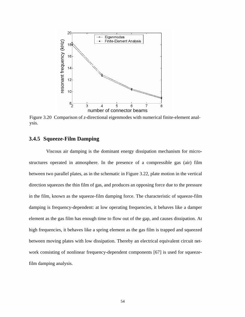
3.4.5 Squeeze-Film Damping
Viscous air damping is the dominant energy dissipation mechanism for micro-
structures operated in atmosphere. In the presence of a compressible gas (air) film
between two parallel plates, as in the schematic in Figure 3.22, plate motion in the vertical
direction squeezes the thin film of gas, and produces an opposing force due to the pressure
in the film, known as the squeeze-film damping force. The characteristic of squeeze-film
damping is frequency-dependent: at low operating frequencies, it behaves like a damper
element as the gas film has enough time to flow out of the gap, and causes dissipation. At
high frequencies, it behaves like a spring element as the gas film is trapped and squeezed
between moving plates with low dissipation. Thereby an electrical equivalent circuit net-
work consisting of nonlinear frequency-dependent components [67] is used for squeeze-
film damping analysis.
number of connector beams
reso
nant
freq
uenc
y (k
Hz)
Figure 3.20 Comparison of z-directional eigenmodes with numerical finite-element anal-ysis.
54

Figure 3.21 Illustration of the first three modes of the actuator by numerical finite-ele-ment analysis.
xy
z
Mode 1: 10.3 kHz, z
Mode 2: 11.7 kHz, x
Mode 3: 32.6 kHz, φ
55

Assume that the gas film undergoes an isothermal process during the entire
motion, the distribution of the gas pressure between plates is governed by the compress-
ible gas-film Reynolds equation [66]. In the analysis given in [65], the plate motion is
assumed to be small, and perpendicular to the surface of two parallel plates, producing the
linearized Reynolds equation:
(3.31)
where p is the pressure change of the static pressure, Pa, g is the static gap spacing, z is the
plate displacement, and is the Laplacian operator. is the effective gas viscosity
given by [67],
(3.32)
where is the viscosity coefficient of air. is the Knudsen number in which λ
is defined as the mean free path of air. (3.32) is suitable for use in both continuum fluid
mechanics when the air gap is much larger than the mean free path of air, and in molecular
air-damping regime when the gap is narrow or/and the pressure is low. At air pressure of
Figure 3.22 Cross-section schematic illustrating a squeezed thin film of gas between twoparallel plates separated by a gap, g, resulted from the vertical motion of the plate withvelocity, v. The squeeze-film damping force, FD, is produced opposing the direction ofmotion.
fixed plate
moving plate
v
FDgz
Pag2
12ηeff---------------∇2 p
Pa------
t∂∂ p
Pa------ –
t∂∂ z
g--- =
∇2 ηeff
ηeffη
1 9.638Kn1.159+
-------------------------------------=
η Kn λ g⁄=
56

1 atm and room temperature of 25 °C, the mean free path is λ = 70 nm and the viscosity
coefficient is = 22.6 µN⋅s/m2.
Squeeze-film damping force is simulated by a lumped parameter model consist-
ing of parallel branches of series-connected nonlinear inductors and resistors [67], as
shown schematically in Figure 3.23. By using the analogy between mechanical and elec-
trical systems, the inductors and resistors are used to represent the spring behavior and the
damping behavior of the gas film. The damping force and plate velocity are analogous to
the through variable (electrical current) and the across variable (electrical voltage). The
components and are given by,
(3.33)
(3.34)
η
Figure 3.23 Equivalent circuit model using nonlinear inductors and resistors forsqueeze-film damping analysis. Damping force and plate velocity are analogous to elec-trical current and voltage in the schematic.
L11
R11
L13 L31
R13 R31
Lmn
Rmn
• • •
• • •
+
_
V (Velocity)
I (Force)
Lmn Rmn
Lmn mn( )2π4g z–( )
64lwPa----------------------=
Rmn mn( )2m
2l2
n2w
2+( ) π6
g z–( )3
768 lw( )3ηeff
-------------------------------=
57

where ( ) is pair of odd integers, and l, w are dimensions of a rectangular plate. For
plate size of tens of microns, non-zero pressure change at the edge is considered using
[68],
(3.35)
and
(3.36)
to replace and in (3.33) and (3.34).
The damping coefficient, b, with respect to the gap spacing, g, is characterized by
performing frequency-domain analysis of the parallel-plate actuator using NODAS simu-
lation. The lumped-parameter actuator model shown in Figure 3.24 uses three squeeze-
film damping elements to represent three parallel plates of different displacements and
velocities. The displacements, zs1 and zs2, of the sensing plates 1 and 2, given by,
(3.37)
(3.38)
are less than the actuation-plate displacement, z, due to the cantilever rotation. l0, l1, and l2
are 183 µm, 153 µm, and 123 µm in design, respectively. k and m are 0.167 N/m and
3.84×10⁻¹¹ kg, as calculated in Section 3.4.3 and 3.4.4. Parameters used in the squeeze-
film damping model are: plate size = 20 × 80 µm2, Pa = 105 Pa, η = 22.5 µN⋅s/m2, and
Kn = 7.052⋅10-8/g (g is in meters). The damping ratio, , is determined by
matching the frequency response of the lumped-parameter model with that of a second-
order transfer function, . The damping ratio ξ is ranging from 240 to 0.2
m n,
leff l g 0.8792 10000 l⋅+( )+=
weff w g 0.8792 10000 w⋅+( )+=
l w
zs1 l1 l0⁄( )z=
zs2 l2 l0⁄( )z=
ξ b 2 mk( )⁄=
1 ms2 bs k+ +( )⁄
58
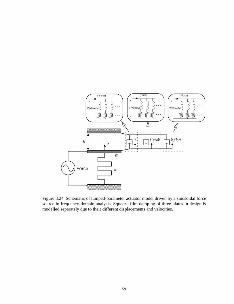
•
•
g z
k
m
• • •
• • •
+
_
V (Velocity)
I (Force)
Figure 3.24 Schematic of lumped-parameter actuator model driven by a sinusoidal forcesource in frequency-domain analysis. Squeeze-film damping of three plates in design ismodelled separately due to their different displacements and velocities.
Force
(l1/l0)z (l2/l0)zz
• • •
• • •
+
_
V (Velocity)
I (Force)
• • •
• • •
+
_
V (Velocity)
I (Force)
59

for gaps between 0.2 µm to 4 µm as shown in Figure 3.25. The designed actuator is over-
damped (ξ > 1) for gaps within 2.1 µm, and becomes underdamped (0 < ξ < 1) beyond
g = 2.1 µm.
3.5 Capacitive Position Sensing
Position of the actuator is detected by the change of the parallel-plate sensing
capacitances, Cs1 and Cs2, formed between the top electrode and the sensing plates 1 and
2, as shown in the actuator side-view schematic in Figure 3.26(a). The equivalent circuit
schematic in Figure 3.26(b) illustrates that capacitance change is converted to a modulated
sensed voltage using a single-ended capacitive bridge, followed by amplification, demod-
ulation, and low-pass filtering of the 1× and 2× carrier-frequency signals. Initial gap spac-
ing, g, is defined from center of the actuation plate to the top electrode, Cs is the sum of
Cs1 and Cs2, Av is the voltage gain of the sensing pre-amp, Vm is the modulation voltage,
Figure 3.25 Damping ratio of parallel-plate actuator versus gap separation at atmosphericpressure.
dam
ping
rat
io (
ξ)
gap (µm)
60

Vc is the carrier voltage, Ad is the voltage conversion gain of the demodulator, and ωp is
the corner (-3 dB) frequency of the low-pass filter with a d.c. gain of 1. The capacitance,
Ci, includes the routing capacitance to the ground and the silicon substrate (an a.c. ground)
throughout the meandering spring, and the pre-amp gate capacitance. Routing capacitance
to the substrate can be neglected because the silicon is at least 30 µm below the actuator
after the post CMOS-MEMS process. After low-pass filtering, a voltage subtracter is used
to remove the d.c. component from the initial sensed signal.
Figure 3.26 (a) Side-view schematic of parallel-plate actuator illustrating capacitivesensing scheme. (b) Equivalent capacitive sensing circuit model.
•
•
•
•
Vm
1
ωp
Low-pass filter
×Pre-amp Demodulator
Av
Sensing plate 2 Sensing plate 1 Actuation plate
+_ Vs
Initial sensed voltage
Cs2 Cs1
Vc
AdCi
g
Top electrode
1
ωp
Low-pass filter
×Pre-amp Demodulator
Av +_
Initial sensed voltage
Vc
Ad
(a)
(b)
CiVm
Cs = Cs1 + Cs2
+_
Vs
+_
subtraction
subtraction
•
•
Cact
61
The magnitude of the sensed voltage output after the low-pass filter is a function
of actuation-plate displacement, z, given by,
(3.39)
where Cs10 and Cs20 are the initial sensing capacitances, εoA/g. The sensing capacitances,
Cs1(z) and Cs2(z), are functions of the sensing-plate displacements in (3.37) and (3.38),
given by,
(3.40)
(3.41)
The capacitive sensor gain at an operating point z = Zo is defined as the differen-
tiation of the sensed output with respect to the actuation-plate displacement. By including
the dominant pole ωp from the low-pass filter, the capacitive sensor transfer function at
z = Zo is,
(3.42)
where
(3.43)
Parameters used in (3.43) are: q1 = l1/l0 = 0.8361, q2 = l2/l0 = 0.6721, Av = 10, Ad = 4.7,
Vm = 1 V, A = 1600 µm2, and ωp = 120 kHz. The extracted capacitance Ci from layout is
Vs AvAd Vm
Cs1 z( ) Cs2 z( )+
Cs1 z( ) Cs2 z( ) Ci+ +--------------------------------------------------
Cs10 Cs20+
Cs10 Cs20 Ci+ +---------------------------------------–
=
Cs1 z( )εoA
g l1 l0⁄( )z–----------------------------=
Cs2 z( )εoA
g l2 l0⁄( )z–----------------------------=
H s( )z Zo=
Gs Zo( )1 s ωp⁄+----------------------=
Gs Zo( )AvAd Vm CiεoA q1 q2+( )g
24q1q2Zog– q1q2 q1 q2+( )Zo
2+[ ]
Ci g q1z–( ) g q2z–( ) εoA 2g q1 q2+( )Zo–( )+[ ]2----------------------------------------------------------------------------------------------------------------------------------------------------=
62
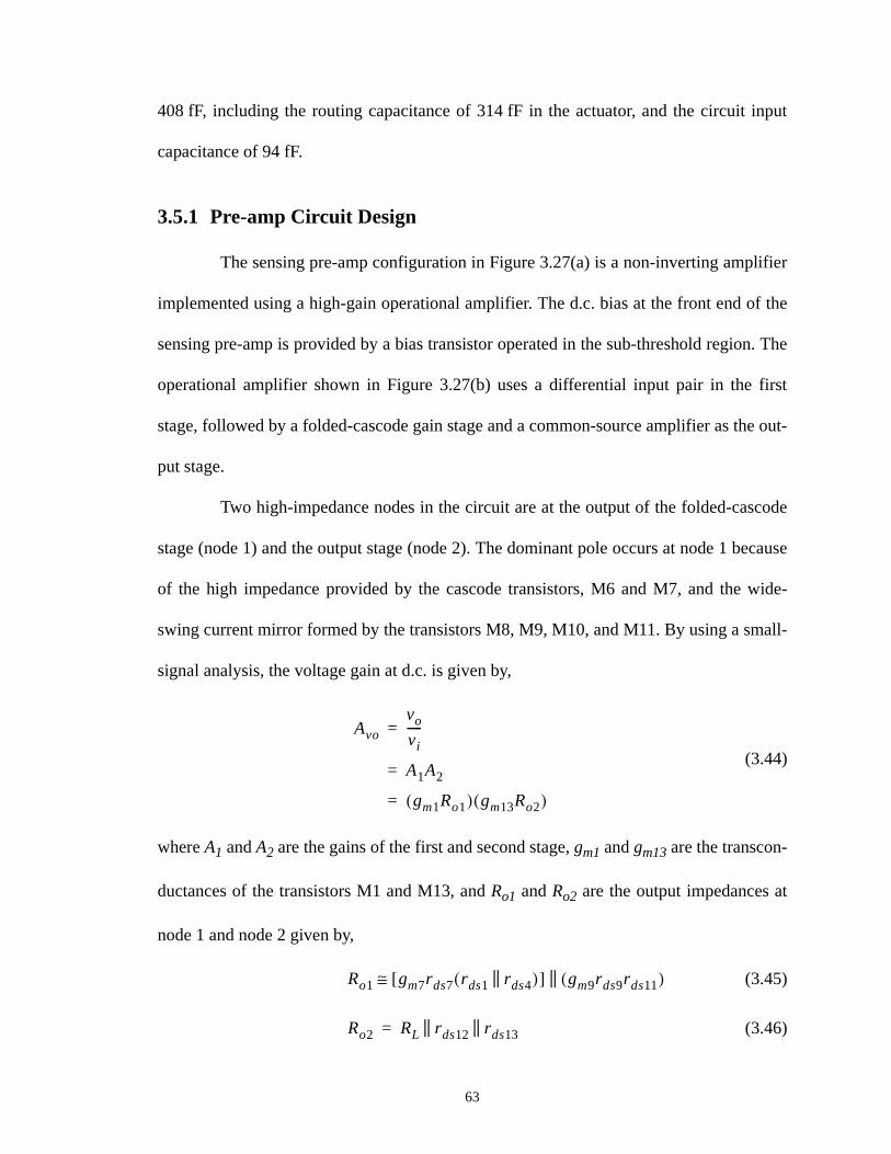
408 fF, including the routing capacitance of 314 fF in the actuator, and the circuit input
capacitance of 94 fF.
3.5.1 Pre-amp Circuit Design
The sensing pre-amp configuration in Figure 3.27(a) is a non-inverting amplifier
implemented using a high-gain operational amplifier. The d.c. bias at the front end of the
sensing pre-amp is provided by a bias transistor operated in the sub-threshold region. The
operational amplifier shown in Figure 3.27(b) uses a differential input pair in the first
stage, followed by a folded-cascode gain stage and a common-source amplifier as the out-
put stage.
Two high-impedance nodes in the circuit are at the output of the folded-cascode
stage (node 1) and the output stage (node 2). The dominant pole occurs at node 1 because
of the high impedance provided by the cascode transistors, M6 and M7, and the wide-
swing current mirror formed by the transistors M8, M9, M10, and M11. By using a small-
signal analysis, the voltage gain at d.c. is given by,
(3.44)
where A1 and A2 are the gains of the first and second stage, gm1 and gm13 are the transcon-
ductances of the transistors M1 and M13, and Ro1 and Ro2 are the output impedances at
node 1 and node 2 given by,
(3.45)
(3.46)
Avo
vo
vi-----=
A1A2=
gm1Ro1( ) gm13Ro2( )=
Ro1 gm7rds7 rds1 rds4||( )[ ] gm9rds9rds11( )||≅
Ro2 RL rds12 rds13|| ||=
63
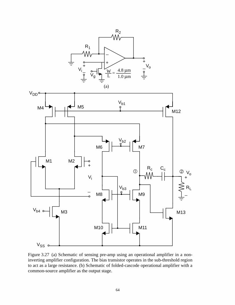
Figure 3.27 (a) Schematic of sensing pre-amp using an operational amplifier in a non-inverting amplifier configuration. The bias transistor operates in the sub-threshold regionto act as a large resistance. (b) Schematic of folded-cascode operational amplifier with acommon-source amplifier as the output stage.
+
_
+_
R2
R1
ViVo+
_
(a)
Vi
VSS
Vb1
Vb2
Rc Cc
Vb3
Vb4
Vo
VDD
+
_
•
•
••
•
••
•
•
•
•
•
+
_
M1 M2
M3
M4 M5
M6 M7
M8 M9
M10 M11
M12
M13
•
•
•
RL
••
•
WL
=4.8 µm1.0 µmVg
64

where rds is the output impedance across the drain and source of transistors, and RL is the
load resistance. The transistor transconductance gm of a MOSFET transistor is given by,
(3.47)
where µ is the carrier mobility, Cox is the gate capacitance per unit area, and IDS is the
drain-to-source current.
To provide sufficient phase margin for the circuit, the dominant pole at node 1 is
moved to a lower frequency away from the second pole by pole-splitting compensation
using the Miller capacitance, Cc. The resistance, Rc, combined with Cc, provides a phase-
lead compensation. The resulting dominant pole after the compensation is given by,
(3.48)
Multiplication of (3.44) and (3.48) yields the gain-bandwidth product,
(3.49)
The circuit is fabricated in the AMS (Austria Micro System) 0.5-µm three-metal-
two-poly CMOS process. The carrier mobility, threshold voltage, channel length modula-
tion parameter, and gate capacitance per unit area for n-channel devices are:
µn = 427 cm2/V⋅s
Vtn = 0.85 V
λn = 0.131 V-1
Cox = 0.0027 F/m2
gm 2µCoxWL-----IDS=
ωp11
Ro1 A2Cc( )--------------------------≅
1Ro1 gm13Ro2Cc( )----------------------------------------=
GBWgm1
Cc--------=
65

, and for p-channel devices:
µp = 112 cm2/V⋅s
Vtp = -0.78 V
λp = 0.036 V-1
Cox = 0.0027 F/m2
The transistor dimensions in design are tabulated in Table 3.5. The compensation resistor,
Rc, and capacitor, Cc, are 720 Ω and 3.54 pF. Each transistor is biased at 400 µA except
for the transistor M3 which is biased at 800 µA. Applying the bias current and the device
parameters through (3.44) to (3.49) yields a open-loop gain of 99.3 dB, and a gain-band-
width product of 64 MHz.
The bias voltages, Vb1, Vb2, Vb3, and Vb4, for the folded-cascode amplifier are
provided by a constant-transconductance bias circuit [69] shown in Figure 3.28. The
drain-source current, IDS3, can be determined by writing a Kirchhoff loop equation for the
transistors M3 and M4,
(3.50)
where the gate-to-source voltage, VGS, is given by,
Transistor, W/L Transistor, W/L Transistor, W/L
M1, 20 µm/0.9 µm M6, 450 µm/1.8 µm M11, 150 µm/1.8 µm
M2, 20 µm/0.9 µm M7, 450 µm/1.8 µm M12, 1730 µm/1.8 µm
M3, 140 µm/1.8 µm M8, 180 µm/1.8 µm M13, 600 µm/1.8 µm
M4, 1040 µm/1.8 µm M9, 180 µm/1.8 µm
M5, 1040 µm/1.8 µm M10, 150 µm/1.8 µm
Table 3.5 Transistor dimensions in the folded-cascode amplifier design.
RbIDS3 VGS4 VGS3–=
66
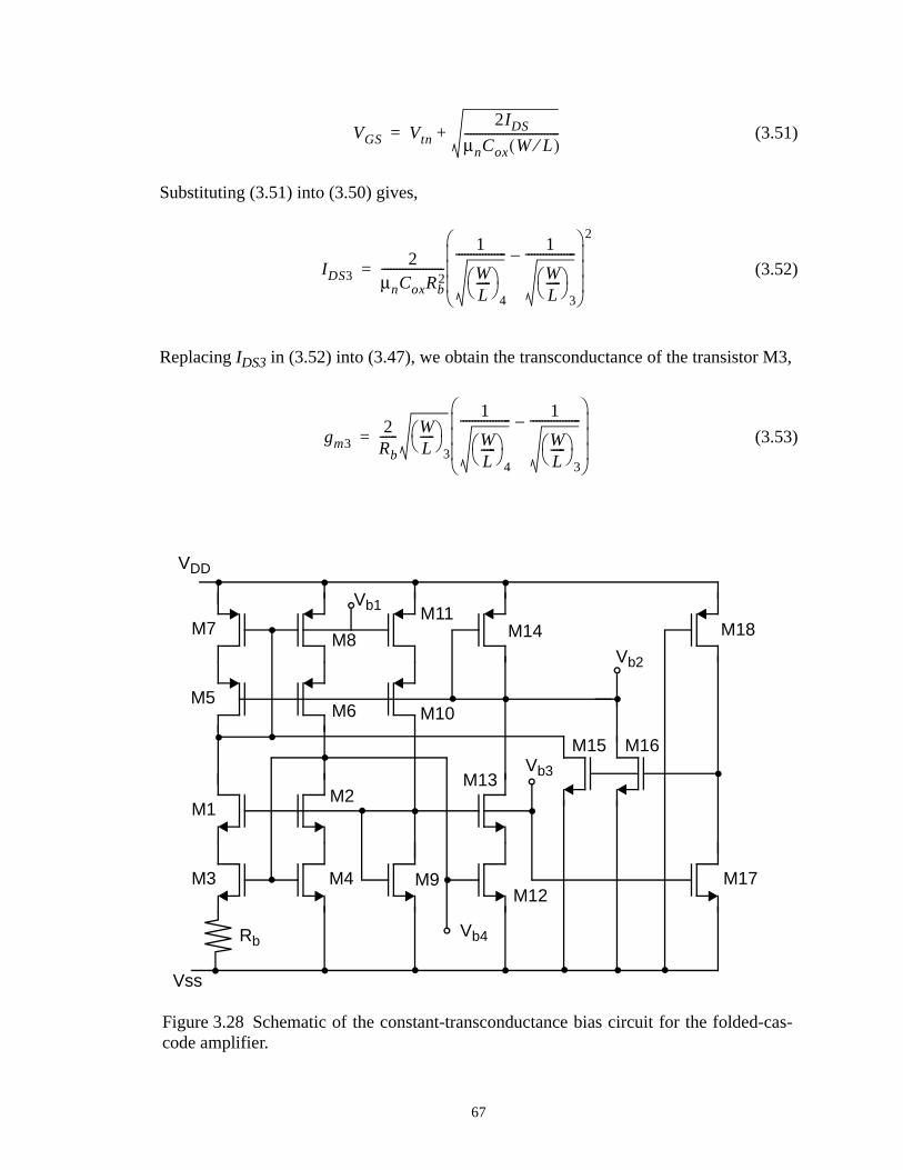
(3.51)
Substituting (3.51) into (3.50) gives,
(3.52)
Replacing IDS3 in (3.52) into (3.47), we obtain the transconductance of the transistor M3,
(3.53)
•
•
•
• • •
••
• •
•
M1M2
M3 M4
M5M6
M7M8
M9
M10
M11
M12
M13
M14
M15 M16
M17
M18
VDD
Vss
Figure 3.28 Schematic of the constant-transconductance bias circuit for the folded-cas-code amplifier.
Vb1
Vb2
Vb4
Vb3
Rb
• • • •
• • • • • • •
•
•
VGS Vtn
2IDS
µnCox W L⁄( )--------------------------------+=
IDS32
µnCoxRb2
---------------------1
WL-----
4
----------------- 1
WL-----
3
-----------------–
2
=
gm32
Rb------ W
L-----
3
1
WL-----
4
----------------- 1
WL-----
3
-----------------–
=
67

which implies that the transconductance of any n-channel transistor biased using this cur-
rent reference is thereby independent of the mobility of the transistor, which varies with
respect to the temperature [70].
The designed transistor dimensions are tabulated in Table 3.6. By applying the
parameters of n-channel devices given in Section 3.5.1 and the transistor sizes in Table 3.6
to (3.53) for a bias current of 400 µA, the biasing resistor, Rb, is found at 306 Ω,
Frequency response of the pre-amp, shown in Figure 3.29, is measured on a sep-
arately bonded test circuit in a dual in-line package (DIP) by the Agilent 4395A spectrum/
network analyzer. The measuring active probe contacts directly with the output pin to
eliminate the use of a coaxial cable, which induces additional capacitive loading to reduce
the measured pre-amp bandwidth. Measured pre-amp gain is 9.85, which is 15% less than
the projected gain of 10. The reason can be the imperfect matching of the on-chip polysil-
icon resistors which are used for setting the closed-loop gain. Measured bandwidth of pre-
amp is 5.7 MHz, which is less than the simulated 8.8 MHz because of capacitive loading
during the measurement.
Transistor, W/L Transistor, W/L Transistor, W/L
M1, 120 µm/1.8 µm M7, 520 µm/1.8 µm M13, 120 µm/1.8 µm
M2, 120 µm/1.8 µm M8, 520 µm/1.8 µm M14, 60 µm/1.8 µm
M3, 180 µm/0.9 µm M9, 120 µm/1.8 µm M15, 10 µm/0.6 µm
M4, 70 µm/0.9 µm M10, 450 µm/1.8 µm M16, 10 µm/0.6 µm
M5, 450 µm/1.8 µm M11, 520 µm/1.8 µm M17, 10 µm/0.6 µm
M6, 450 µm/1.8 µm M12, 70 µm/1.8 µm M18, 1.2 µm/10 µm
Table 3.6 Transistor dimensions in the constant-transconductance bias circuit.
68
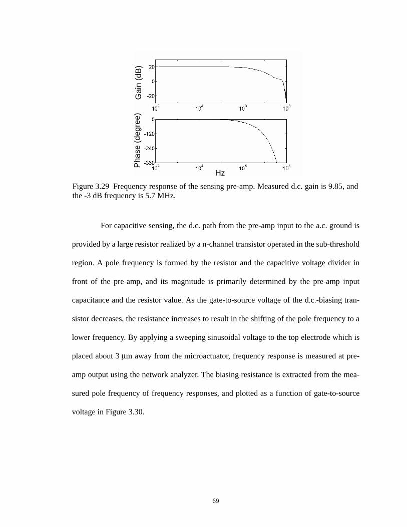
For capacitive sensing, the d.c. path from the pre-amp input to the a.c. ground is
provided by a large resistor realized by a n-channel transistor operated in the sub-threshold
region. A pole frequency is formed by the resistor and the capacitive voltage divider in
front of the pre-amp, and its magnitude is primarily determined by the pre-amp input
capacitance and the resistor value. As the gate-to-source voltage of the d.c.-biasing tran-
sistor decreases, the resistance increases to result in the shifting of the pole frequency to a
lower frequency. By applying a sweeping sinusoidal voltage to the top electrode which is
placed about 3 µm away from the microactuator, frequency response is measured at pre-
amp output using the network analyzer. The biasing resistance is extracted from the mea-
sured pole frequency of frequency responses, and plotted as a function of gate-to-source
voltage in Figure 3.30.
Figure 3.29 Frequency response of the sensing pre-amp. Measured d.c. gain is 9.85, andthe -3 dB frequency is 5.7 MHz.
Hz
Gai
n (d
B)
Pha
se (
degr
ee)
69

3.5.2 Double-Balanced Demodulator
Demodulation of the amplitude-modulated sensed signal after the pre-amp is
realized off the microactuator chip by a BJT (Bipolar Junction Transistor) double-bal-
anced demodulator, the so-called Gilbert cell [71] shown schematically in Figure 3.31.
The advantage of using a double-balanced demodulator over a single-balanced demodula-
tor is that the differential pairs of Q3-Q4, and Q5-Q6 add the amplified carrier-signal
feedthrough with opposite phases, thereby providing a first-order cancellation which leads
to a less demanding low-pass filtering following the demodulation. To increase the linear
input range for operation, emitter degeneration is utilized by adding the resistor, RE, in the
lower emitter-coupled pair, Q1 and Q2. By applying a sufficiently large carrier signal to
the cross-coupled transistors, Q3-Q6 and Q4-Q5, each pair conducts current alternatively
to generate output across the load resistance, RL.
VGS (V)
resi
stan
ce (
Ω)
Figure 3.30 Measured resistance of subthreshold biasing transistor versus gate-to-sourcevoltage.
70

The collector currents, Ic1 and Ic2, of the transistors, Q1 and Q2, can be deter-
mined by numerically solving the following equations from a large-signal analysis,
(3.54)
(3.55)
where Vi is the amplitude of the input signal voltage, α is the base transport factor (ideally
α → 1), and VT is the thermal voltage (VT ≈ 26 mV at 300°K). The voltage conversion
gain, Ad, is the product of the difference of Ic1 and Ic2, and the load resistance, RL, divided
by the input signal, Vin, and a factor of 2 due to the multiplication of Vi(t) by a sinusoidal
carrier signal sin(ωct):
IE
RE
+
_
Vc (carrier)
+
_
RLRL
Q1 Q2
Q3 Q4 Q5 Q6
Figure 3.31 Gilbert multiplier with emitter degeneration applied to improve input volt-age range.
Vi (signal)
RE
+_ Vo
Ic1
Ic2------
Vi RE α⁄( ) Ic1 Ic2–( )–
VT-------------------------------------------------------exp=
Ic1 Ic2+ αIE=
71

(3.56)
By applying the parameters: α = 0.99, IE = 10.6 mA, RE = 75 Ω, and RL = 750 Ω from
(3.54) to (3.56), the voltage conversion gain is calculated from 4.62 to 4.7 for an input
voltage range between 400 to 800 mV. Measured voltage conversion gain is between 4.9
to 5, which is about 6% higher than calculations.
3.6 Noise Analysis and Minimum Detectable Signal
3.6.1 Pre-amp Noise
The primary noise sources in the folded-cascode opamp shown in Figure 3.27(b)
are the transistor pairs M1-M2 and M4-M5 in the differential-input circuit, and M10-M11
in the cascode stage. The transistors M1-M2, M4-M5, and M10-M11 are assumed to be
matched in the following derivations. By adding a voltage noise source at the input of
these transistors, the contributed output noise voltage from the folded-cascode operational
amplifier is given by,
(3.57)
where Vn1, Vn4, and Vn11 are the input noise voltage source of the transistors M1, M4, and
M11. The output noise voltage is related back to an equivalent input noise voltage, Vneq,
by dividing it by the gain squared given in (3.44):
(3.58)
Ad
Ic1 Ic2–( )RL
2Vin-------------------------------=
Vno2 2 gm1Ro1gm13Ro2( )2Vn1
2 2 gm4Ro1gm13Ro2( )2Vn42+=
2 gm11Ro1gm13Ro2( )2Vn112+
Vneq2 2Vn1
2 2gm4
gm1--------
2Vn4
2 2gm11
gm1-----------
2Vn11
2+ +=
72

The input-referred voltage noise source for a MOSFET transistor are represented prima-
rily as the sum of the thermal noise (white noise) and the flicker (1/f) noise at the low fre-
quencies. By using a sufficiently high modulation frequency (> 1 MHz) [72] for capacitive
sensing, the 1/f noise is assumed to be out of the signal frequency range and can be
neglected, leading to,
(3.59)
where i is the transistor index, kB is the Boltzmann’s constant (1.38×10⁻²³ J/K), and T is
the temperature in Kelvins (T = 300 K at room temperature). Applying the device parame-
ters given in Section 3.5.1 to (3.57), (3.58), and (3.59), we obtain the equivalent input-
referred noise voltage Vneq = 9.23 nV/√Hz.
To calculate the equivalent input-referred noise voltage of the entire pre-amp, an
equivalent noise model shown in Figure 3.32 is used with thermal noise of the resistors R1
and R2 being represented by current noise sources, In1 and In2, and thermal noise of the
Vni2 4kBT
23--- 1
gmi------- =
+
_
+_
R2R1
VneqVno_total
In2
In1
∗
•
••
•
••
Figure 3.32 Equivalent pre-amp noise model.
∗ Vn3
Vg
73
d.c.-bias transistor is represented by a voltage noise source, Vn3, where the transistor is
modelled as an equivalent resistor, R3. They are given by,
(3.60)
(3.61)
(3.62)
The equivalent input-referred noise voltage of the pre-amp is given by,
(3.63)
Substituting R1 = 1.517 kΩ, R2 = 13.65 kΩ, and R3 = 100 ΜΩ through (3.60) to (3.63), we
obtain Vneq,total = 1.29 µV/√Hz, which is primarily contributed from the d.c.-bias resistor
R3.
To determine the minimum input-referred noise capacitance change and the min-
imum input-referred noise displacement from the input-referred noise voltage, Vneq,total ,
the relations between the capacitance change and the sensed output voltage, and between
the displacement and the sensed output voltage are derived. Substitution of a small capac-
itance change, ∆C = (Cs1 + Cs2) - (Cs10 + Cs20), into (3.39) leads to the linearized relation
between the capacitance change and the sensed output voltage amplitude,
(3.64)
Equations (3.40) and (3.41) can be re-written with a small actuation-plate displacement, z,
around the initial gap, g,
In12 4kBT
R1------------=
In22 4kBT
R2------------=
Vn32
4kBTR3=
Vneq total,2
Vneq2
Vn32
In12
In22
+( )+R1
2R2
2
R1 R2+( )2--------------------------⋅+=
∆CVs-------- 1
AvAd Vm---------------------- C10 C20 Ci+ +( )=
74

(3.65)
(3.66)
Substitution of (3.65) and (3.66) into (3.39) leads to the linearized relation between the
displacement and the sensed output voltage amplitude,
(3.67)
where the d.c.-bias resistor can be neglected because its magnitude is 102 to 103 times
higher than the impedance value of pre-amp input capacitance at selected modulation fre-
quency. Replacing the sensed voltage in (3.70) and (3.71) with the output noise voltage,
AvAdVneq,total, we find the input-referred noise capacitance change,
(3.68)
and the input-referred noise displacement,
(3.69)
By substituting the parameters: , C10 = C20 = 8.854×10-12×(1600 µm2)/g,
Ci = 408 fF, and Vneq,total = 1.29 µV/√Hz, in (3.68) and (3.69), the minimum input-
referred noise capacitance change and the minimum input-referred noise displacement are
plotted as a function of gap in Figure 3.33(a) and (b). The minimum input-referred noise
capacitance change is larger at smaller gaps, illustrating the difficulty to sense small
capacitance change out of large initial sensing capacitances. However, the minimum
Cs1 C10 1 q1zg---+
≅
Cs2 C20 1 q2zg---+
≅
zVs-------- 1
AvAd Vm----------------------
C10 C20 Ci+ +( )g
q1C10 q2C20+-------------------------------------------=
∆Cn2 1
Vm2
------------ C10 C20 Ci+ +( )2Vneq total,2=
zn2 1
Vm2
------------C10 C20 Ci+ +( )2g2
q1C10 q2C20+( )2-------------------------------------------------Vneq total,
2=
Vm 1=
75

Figure 3.33 (a) Minimum input-referred noise capacitance change versus gap. (b) Mini-mum input-referred noise displacement versus gap.
aF Hz
--------
---
gap (µm)
gap (µm)
(a)
(b)
nm H
z----
-------
inpu
t-re
ferr
ed n
oise
cap
acita
nce,
inpu
t-re
ferr
ed n
oise
dis
plac
emen
t,
76

input-referred noise displacement reduces with the decrease of gap because of the large
capacitive sensor gain at small gaps.
3.6.2 Brownian Noise
Air molecules impinging on the micromechanical plates gives rise to a Brownian
noise force, , which is related to the damping coefficient, b, of the plate as given by
[73],
(3.70)
The damping coefficient can be expressed in terms of the damping ratio, ξz, the actuator
resonant frequency, ωz, and the mass, m, by
(3.71)
Substitution of (3.71) into (3.70) gives,
(3.72)
Multiplication of the Brownian noise force with the frequency response of the actuator
leads to the frequency response of the noise plate displacement given by,
(3.73)
Substituting the actuator parameters: m = 3.84×10⁻¹¹ kg, ωz = 10.5 kHz, and ξz in Figure
3.25, we obtain the equivalent d.c. Brownian noise displacement ranging from 2.69 × 10⁻²
nm/√Hz to 7.75×10⁻⁴ nm/√Hz for gaps between 0.2 µm to 4 µm as shown in Figure 3.34.
Also shown in Figure 3.34 is the equivalent pre-amp noise displacement plotted in Figure
fn2
fn2 4kBTb=
b 2ξzωzm=
fn2 8kBTξzωzm=
zb2
8kBTξz
mωz3
----------------- 11 ω2 ωz
2⁄–( )2 2ξzω ωz⁄( )2+---------------------------------------------------------------------- =
77

3.33(b). The comparison shows that for open-loop system, the minimum detectable signal
is limited by the Brownian noise for gaps below around 0.6 µm at the atmospheric pres-
sure. For the closed-loop system, the Brownian noise force acting on the plates is analo-
gous to a plant-input disturbance. The resultant noise displacement can be lowered by
applying a large open-loop gain.
Figure 3.34 Equivalent Brownian noise displacement of the micromechanical actuatorand equivalent noise displacement derived from pre-amp noise plotted as a function ofgap.
gap (µm)
nm H
z----
-------
equi
vale
nt n
oise
dis
plac
emen
t,
78

Chapter 4
Controller Design
4.1 Introduction
The controller design for parallel-plate servo uses linearization and input-distur-
bance rejection techniques to cope with the nonlinearity and open-loop instability of the
plant. In this chapter, we will first review the classical frequency-domain design method-
ology with focus on quantification of essential feedback properties and their trade-offs
imposed by a given unstable plant. It is beneficial to understand the cost of feedback for
linear unstable plants, such as bandwidth requirement and noise amplification, before
designing for the nonlinear unstable plant. Phase margin of the linearized open-loop trans-
fer function is optimized along the plate motion trajectory by use of a proportional-gain
controller. Effects of initial conditions (i.e., plate acceleration and velocity) and displace-
ment perturbation are modelled as an input-disturbance force into the linearized system.
Disturbance rejection is performed for sensitivity reduction with respect to the disturbance
force. Those techniques are applied in the Quantitative Feedback Theory (QFT), in which
lots of plant uncertainties can be considered for analysis of stability robustness.
4.2 Classical Frequency-Domain Feedback Theory
Feedback control is used to stabilize unstable plants, to reduce the sensitivity
with respect to external disturbance, and to reduce the effect from variations of plant
parameters. On the other hand, potential disadvantages also exist. Improper controller
design can destabilize systems when plants are stable. Large loop bandwidth can induce
79

excessive sensor noise at the plant input to deteriorate stability robustness as well. All
these properties have to be quantified to understand design limitations and trade-offs,
especially for design of unstable plants.
4.2.1 Quantification of Feedback Performance
Consider the linear time-invariant closed-loop feedback system shown in Figure
4.1, where P(s) is the plant, C(s) is the controller, r(s) is the command input, y(s) is the
system output, d1(s) is the disturbance at plant input, d2(s) is the disturbance at plant out-
put, and n(s) is sensor noise.
Define the open-loop transfer function,
(4.1)
the sensitivity function,
(4.2)
and the complementary sensitivity function,
(4.3)
Figure 4.1 Block diagram of a linear time-invariant feedback system. Adequate control-ler design rejects input and output disturbances (d1, d2), and avoids noise (n) amplifica-tion.
C(s) P(s)
n(s)
d1(s) d2(s)
r(s) y(s)+_ ++
++
++
L s( ) C s( )P s( )=
S s( ) 11 L s( )+--------------------=
T s( ) L s( )1 L s( )+--------------------=
80
By linear superposition, the outputs of the system contributed from r, d1, d2, and n are
summed up and represented by the sensitivity and complementary sensitivity functions,
(4.4)
where
(4.5)
(4.6)
(4.7)
and
(4.8)
Similarly, the input to the plant is
(4.9)
where
(4.10)
(4.11)
(4.12)
and
(4.13)
Classical design by shaping of open-loop transfer function indirectly alters the
feedback properties (sensitivity and complementary sensitivity functions) of the system.
Rules of thumb for shaping the open-loop transfer function use a large loop gain at low
frequencies for sensitivity reduction and disturbance rejection, and a small loop gain at
y s( ) yr s( ) yd1 s( ) yd2 s( ) yn s( )+ + +=
yr s( ) T s( )r s( )=
yd1 s( ) P s( )S s( )d1 s( )=
yd2 s( ) S s( )d2 s( )=
yn s( ) T s( )n s( )–=
u s( ) ur s( ) ud1 s( ) ud2 s( ) un s( )+ + +=
ur s( ) C s( )S s( )r s( )=
ud1 s( ) S s( )d1 s( )=
ud2 s( ) C s( )S s( )d2 s( )–=
un s( ) C s( )S s( )n s( )–=
81

high frequencies to achieve small noise response. Phase margin is determined by the roll-
off rate of loop gain at the vicinity of the crossover frequency. Large phase margin avoids
amplification of disturbances and noise, given that,
(4.14)
It is not desirable to have a large loop gain at frequencies for which the plant
gain is small. The gains of (4.12) and (4.13) reduce to at those frequencies,
thereby inducing large responses at the plant input due to output disturbance and noise.
4.2.2 Analysis of Unstable Plant
4.2.2.1 Stability Criterion
Given a feedback system whose open-loop transfer function, , is strictly
proper with possible poles and/or zeros on the axis, and poles in the right-half
plane, the Nyquist stability criterion is given as the follows:
Theorem 4.1 Define the standard Nyquist contour, , as the semi-circle of radius in
the clockwise direction with necessary -axis indentations to account for the imaginary
poles of . Let be the ray connecting between ( ]. The crossing
between and the locus is said to be positive if the direction is counter-clockwise,
and negative otherwise, as shown in Figure 4.2(a). The feedback system is stable, if and
only if the Nyquist plot of does not intersect -1 + j0, and the net sum of its crossings
of Ro is equal to [74].
L jω( ) 1 L jω( )∠, 180°–≅= S jω( ) 1 T jω( ) 1»,»⇔
P1–
s( )
L s( )
jω n s
Γ R
jω
L s( ) Ro ∞– 1– j0+,
Ro L s( )
L s( )
n
82

For stability analysis on the Nichols chart, the criterion is modified as the follow-
ing [75]:
Theorem 4.2 Let be the ray defined as R1 = (φ, r) | φ = , r > 0 dB. The cross-
ing between and the locus of on the Nichols chart is said to be positive if the
direction is counter-clockwise, and negative otherwise as shown in Figure 4.2(b). The
feedback system is stable, if and only if does not intersect the point ( , 0 dB),
and the net sum of its crossings of R1 is equal to .
4.2.2.2 Bandwidth Limitations with a Real Unstable Pole
Stabilization of a linear unstable plant requires pulling of unstable poles from the
right-half complex plane into the left half plane, thereby implying a lower-bounded open-
loop gain. The Bode gain-phase relation [76] states that loop gain must not decrease faster
than 40 dB/decade, indicating that the resultant crossover frequency is also lower-bounded
Figure 4.2 (a) The notion of crossing with the ray between ( ] on the com-plex plane. (b) The notion of crossing on the Nichols chart, where the ray is defined as R1
= dB.
∞– 1– j0+,
φ r,( ) φ 180– ° r 0>,=
-1
Ro
degree
open
-loop
gai
n (d
B)
(b)(a)
__
++
real
imag R1
L(s)
R1 180– °
R1 L s( )
L s( ) 180– °
n
83
for stabilizing an unstable plant. To illustrate the increase of crossover frequency, let the
open-loop transfer function containing one unstable pole be given by,
(4.15)
where is the stable part of the unstable open-loop function , and is an
unstable all-pass function with gain of one throughout all frequencies. The phases of
and at the crossover frequency are given by,
(4.16)
, (4.17)
where is the phase margin of open-loop function . To obtain the same amount of
phase margin for and , comparing (4.16) and (4.17) gives,
(4.18)
is the allowed phase lag at the crossover frequency by for loop-gain roll-off
in the stable case. By applying (4.18) to obtain the same amount of phase lag for loop-gain
decrease in the unstable case, the crossover frequency, , should be at least twice as
large as the unstable pole frequency [77].
L s( ) P s( )C s( )=
Ps s( )s a–-------------C s( )=
Ps s( )C s( )s a+
------------------------- s a+s a–-----------⋅=
Ls s( )A s( )=
Ls s( ) L s( ) A s( )
Ls jω( ) L jω( ) ωc
Ls jωc( )∠ 180– θm+=
L jωc( )∠ Ls jωc( ) 180– 2θ ω ωc=+∠= θtan
ωc
a------=
θm Ls s( )
Ls s( ) L s( )
Ls jωc( )∠ 2θ ω ωc=– θm+=
Ls jωc( )∠ Ls
ωc
84

4.2.2.3 Unstable Poles and the Sensitivity Function
For stable open-loop with at least two more poles than zeros, there will
always exist a frequency range over which sensitivity function in (4.2) is greater than one,
as will have a phase lag of at least for ω → ∞. A graphical illustration of the
sensitivity function magnitude on the complex plane is in Figure 4.3. According to the
Bode sensitivity integral, the sensitivity function must satisfy [78],
(4.19)
which implies that a trade-off exists between sensitivity properties in different frequency
ranges, since the area of sensitivity reduction must be equal to the area of sensitivity
increase in units of decibels × (rad/sec).
When has poles in the open right half plane, denoted by pi: i = 1,...,n, the
sensitivity function will instead satisfy [78],
L s( )
L s( ) 180°–
Figure 4.3 Graphical illustration of the sensitivity function magnitude for L(s) having atleast two more poles than zeros. Sensitivity is larger than one when L(s) enters the unitcircle centered at -1 + j0.
-1
|S(jω)| > 1
|S(jω)| < 1
L(jω)
real
imag
S jω( )log ωd0
∞
∫ 0=
L s( )
85
(4.20)
which implies that the area of sensitivity increase is larger than the area of sensitivity
reduction by an amount proportional to the distance of unstable poles to the origin. The
amount of difference can also be interpreted as the required open-loop gain to pull the
unstable poles into the left half complex plane. This open-loop gain can otherwise be used
for sensitivity reduction if all poles are stable. However, (4.20) does not give any design
implication regarding design trade-offs and limitations. By combining (4.20) and con-
straints on crossover frequency, loop-gain roll-off rate, and required sensitivity reduction,
the peak value of the sensitivity function was derived by Freudenberg [78]. Let have
a frequency-dependent bound after the crossover frequency given by,
(4.21)
where ε < 1/2 and the roll-off rate k > 0. The sensitivity function is required to satisfy an
upper bound for ,
(4.22)
(4.20) is manipulated to satisfy both constraints from (4.21) and (4.22), giving
sup , (4.23)
(4.23) quantifies the largest peak value of the sensitivity function occurs at frequencies
between and due to either of the following reasons: 1) these two frequencies are
S jω( )log ωd0
∞
∫ π Re pi[ ]i 1=
n
∑=
L s( )
L jω( ) εωc
ω------
1 k+
ω ωc≥∀,≤
ω ωo≤
S jω( ) Ms 1 ω ωo ωc≤ ≤∀,<≤
S jω( ) 1ωc ωo–------------------ π Re pi[ ] ωo
1Ms------ 3εωc
2k------------–log+
i 1=
n
∑
≥log ω ωo ωc,( )∈
ωo ωc
86

very close, 2) the distance of unstable poles to the origin is large, 3) a small is required
for sensitivity reduction, and 4) the roll-off rate is fast. Hence a design trade-off is
imposed by the bandwidth constraint from (4.21) and the peak sensitivity constraint from
(4.23).
4.2.2.4 Unstable Poles and the Complementary Sensitivity Function
Two types of frequency-dependent bounds are used to limit the gain of the com-
plementary sensitivity function at high frequencies for noise reduction. They are,
(4.24)
and
(4.25)
Denote a real unstable pole of , p1, and is the angle from the crossover frequency
on the imaginary axis to the pole.
= tan-1 (4.26)
Based on the roll-off rate constraint in (4.24), Looze [79] derived the peak value of the
complementary function,
sup (4.27)
where Cl2(⋅) is the Clausen integral,
(4.28)
Ms
T jω( )ωc
ω------
k
ω ωc≥∀,≤
T jω( ) Mt 1 ω ωc≥∀,≤ ≤
L s( ) φ
φωc
p1------
T jω( )log k
φ( )tan( ) π2--- φ– 1
2---Cl2 2φ( ) 1
2---Cl2 π 2φ–( )+ +log–
φ------------------------------------------------------------------------------------------------------------------------ ω 0>∀,⋅≥
Cl2 θ( ) 2x2--- sin
log xd0
θ
∫–=
87

Based on the high-frequency constraint in (4.25), the peak value of the complementary
function is constrained by,
sup (4.29)
A design trade-off is imposed by the roll-off rate, k, from (4.24) and the comple-
mentary sensitivity peak from (4.27), as shown graphically in Figure 4.4. (4.29) is used
with = 0.5 to plot for the curve of k = 0. As discussed in Section 4.2.2.2, a rule of
thumb states that the crossover frequency should be at least twice as large as the unstable
pole frequency, which results in a minimum peak value of |T(jω)| less than 4 dB with a
one-pole roll-off as shown in Figure 4.4. It is desirable to minimize the peak value in order
to maximize phase margin as indicated by (4.14).
T jω( )log
1Mt------ π
2--- φ– log
φ-------------------------------------- ω 0>∀,≥
Mt
Figure 4.4 Minimum complementary sensitivity peak versus ratio of crossover fre-quency to unstable pole frequency. A rule of thumb for design requires that the crossoverfrequency at least twice as large as the unstable pole frequency with an one-pole rolloff toreduce the resultant peak within 4 dB.
|T(jω
)|m
in (d
B)
crossover frequency/unstable pole, ωc/p1
88

4.3 Controller Design by Linearization
For given small signals, a nonlinear system behaves similarly to its linearized
approximation at each operating point. Local stability is analyzed using the frequency-
domain method with phase margin and gain margin, as opposed to the Lyapunov’s linear-
ization method [80] for the state-space approach in which stability is ensured by placing
all the closed-loop poles in the left-half complex plane.
Input-command shaping and input-disturbance rejection are utilized to extend
local stability around an operating point to global stability as needed in a position-servo
problem. Input command shaping ensures that the nonlinear plant behaves mostly like the
linearized plants around a time-varying operating point. Input-disturbance rejection
reduces the effects of initial conditions and neglected high-order electrostatic force terms
during linearization of the nonlinear plant.
A two-degree-of-freedom control system configuration is used for realizing the
design procedures stated above. The nonlinear plant is linearized in the stable and unstable
regimes, and the maximum phase margin is analyzed using a proportional-gain controller.
Controller design regarding the input-disturbance rejection, steady-state error, and shock-
force rejection are presented following the stability analysis.
4.3.1 Two-Degree-of-Freedom Control Systems
Two types of trade-off exist in controller design between the sensitivity and com-
plementary sensitivity functions. One is the algebraic trade-off at each frequency, as evi-
denced by the relation,
(4.30)S jω( ) T jω( )+ 1=
89
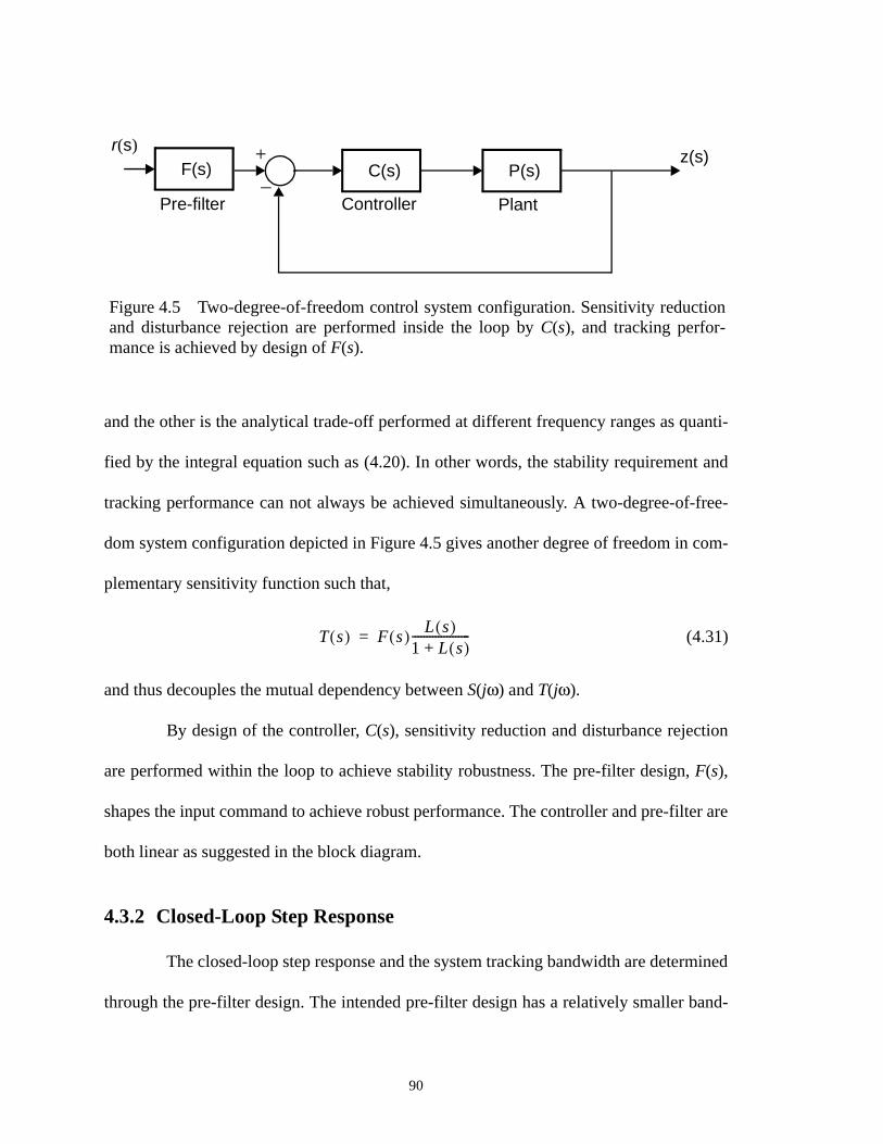
and the other is the analytical trade-off performed at different frequency ranges as quanti-
fied by the integral equation such as (4.20). In other words, the stability requirement and
tracking performance can not always be achieved simultaneously. A two-degree-of-free-
dom system configuration depicted in Figure 4.5 gives another degree of freedom in com-
plementary sensitivity function such that,
(4.31)
and thus decouples the mutual dependency between S(jω) and T(jω).
By design of the controller, C(s), sensitivity reduction and disturbance rejection
are performed within the loop to achieve stability robustness. The pre-filter design, F(s),
shapes the input command to achieve robust performance. The controller and pre-filter are
both linear as suggested in the block diagram.
4.3.2 Closed-Loop Step Response
The closed-loop step response and the system tracking bandwidth are determined
through the pre-filter design. The intended pre-filter design has a relatively smaller band-
T s( ) F s( ) L s( )1 L s( )+--------------------=
Figure 4.5 Two-degree-of-freedom control system configuration. Sensitivity reductionand disturbance rejection are performed inside the loop by C(s), and tracking perfor-mance is achieved by design of F(s).
C(s) P(s)
r(s)z(s)+
_F(s)
Plant Controller Pre-filter
90
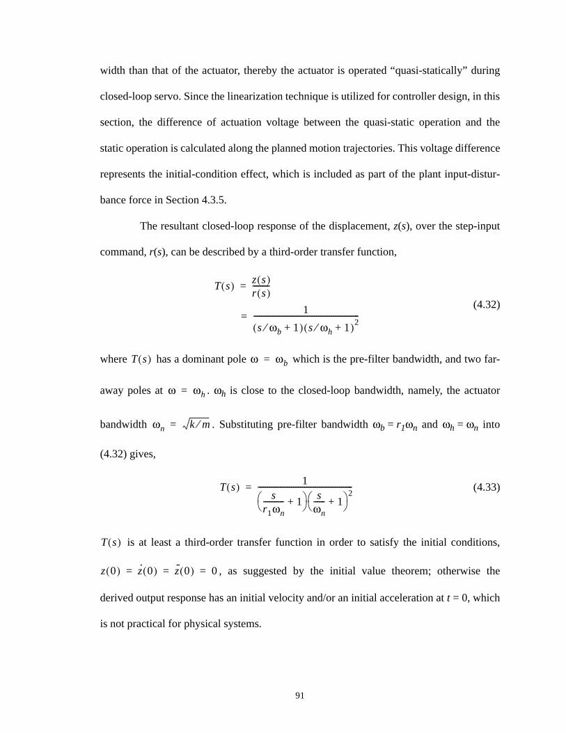
width than that of the actuator, thereby the actuator is operated “quasi-statically” during
closed-loop servo. Since the linearization technique is utilized for controller design, in this
section, the difference of actuation voltage between the quasi-static operation and the
static operation is calculated along the planned motion trajectories. This voltage difference
represents the initial-condition effect, which is included as part of the plant input-distur-
bance force in Section 4.3.5.
The resultant closed-loop response of the displacement, z(s), over the step-input
command, r(s), can be described by a third-order transfer function,
(4.32)
where has a dominant pole which is the pre-filter bandwidth, and two far-
away poles at . ωh is close to the closed-loop bandwidth, namely, the actuator
bandwidth . Substituting pre-filter bandwidth ωb = r1ωn and ωh = ωn into
(4.32) gives,
(4.33)
is at least a third-order transfer function in order to satisfy the initial conditions,
, as suggested by the initial value theorem; otherwise the
derived output response has an initial velocity and/or an initial acceleration at t = 0, which
is not practical for physical systems.
T s( ) z s( )r s( )---------=
1
s ωb⁄ 1+( ) s ωh⁄ 1+( )2---------------------------------------------------------=
T s( ) ω ωb=
ω ωh=
ωn k m⁄=
T s( ) 1s
r1ωn----------- 1+ s
ωn------ 1+ 2
---------------------------------------------------=
T s( )
z 0( ) z· 0( ) z·· 0( ) 0= = =
91

The closed-loop transient response is determined by the selection of pre-filter,
and can be approximated by applying a displacement step input command to this third-
order closed-loop transfer function. Substituting into (4.33) and apply-
ing the inverse Laplace transform gives,
(4.34)
and can be obtained accordingly by differentiations of (4.34). Dividing (4.34) by
the initial gap, g, and using the normalized time axis = , we obtain the normalized
displacement,
(4.35)
where , αmax = Zo,max/g, and α = Zo/g is the normalized displacement. Re-
arranging the parallel-plate dynamic equation in (3.4) with the normalized displacement
yields the applied voltage,
(4.36)
where the damping ratio . To calculate the steady-state actuation voltage
for displacement up to αmaxg, we remove the dynamic terms in (4.36). The steady-state
actuation voltage for normalized displacements between [0, Zo,max/g] is,
(4.37)
r s( ) Zo max, s⁄=
z t( ) Zo max, 11
1 r1–------------- 2
er1ωnt–
–r1 2–( )r1
1 r1–( )2-----------------------
r1ωnt
r1 1–-------------+
eωnt–
–
=
z· t( ) z·· t( )
τ ωnt
z τ( ) αmax 1r2
r2 r1–---------------
2e
r1τ––
r1 2r2–( )r1
r2 r1–( )2-----------------------------
r1r2τr1 r2–---------------+
er2τ–
–
=
z τ( ) z τ( ) g⁄=
z τ( )
V τ( ) 1 z τ( )–( )g2mgεoA-----------
τ
2
dd z τ( ) 2ξωn τd
d z τ( ) ωn2 z τ( )+ +
⋅=
ξ b 2 mk( )⁄=
Vss 1 α–( )ωng2mgεoA-----------α⋅=
92
From (4.36) and (4.37), the ratio of the voltage difference between the transient and
steady-state voltages over the steady-state voltage at each normalized position is given
by,
(4.38)
The ratio of the maximum transient voltage, , over static actuator pull-in voltage
in (3.8) is,
(4.39)
The plant parameters given in Chapter 3 and a target displacement of 90% of the
initial gap (g = 3 µm) are substituted in (4.35) and (4.38) for slow closed-loop responses
(r1 = 0.05 to 0.2) and fast closed-loop responses (r1 = 0.25 to 1). The voltage differences
of quasi-static and static operations are plotted in Figure 4.6(a) and (b) as a function of
normalized displacement. Both graphs shows that the difference increases as the closed-
loop response becomes faster. In addition, the responses exhibit mostly transient behavior
at small displacements to provide initial acceleration for the plate, and the difference
increases again at large displacements due to the increasing damping ratio. We will per-
form the position servo for ωb less than 0.05 ωn to meet the quasi-static conditions used by
the linearization technique. The deviation from a linear operation shown in Figure 4.6, is a
initial condition which is considered in Section 4.3.5 as an input disturbance to the linear-
ized plant.
β
V τ( ) Vss–
Vss-------------------------
1 z τ( )–( ) 1ωn
2------
τ
2
dd
z τ( )( )2ξωn------
τdd z τ( ) z τ( )+ +
1 α–( ) α–
1 α–( ) α----------------------------------------------------------------------------------------------------------------------------------------------=
Vmax Vpi
Vmax
Vpi----------- 3 3
2---------- max 1 z τ( )–( ) 1
ωn2
------τ
2
dd
z τ( )( )2ξωn------
τdd z τ( ) z τ( )+ +
⋅ τ∀ τ 1≤, ,=
93

(a)
(b)
Figure 4.6 Percentage ratio of the voltage difference between the transient and steady-state responses as a function of normalized displacement. (a) tracking bandwidthωb = 0.05ωn to 0.2ωn. (b) tracking bandwidth ωb = 0.25ωn to ωn.
[(V
(τ)
- V
ss)/
Vss
]%[(
V(τ
) -
Vss
)/V
ss]%
ωb/ωn = 0.200.150.10
0.05
ωb/ωn = 1.000.750.500.25
Zo/g
Zo/g
94

We also apply the plant parameters into (4.39) and plot in Figure 4.7 the ratio of
the maximum transient voltage over the static pull-in voltage as a function of the tracking
bandwidth. A maximum supplied voltage about five times of the static pull-in voltage is
required to servo the actuator at its mechanical bandwidth.
4.3.3 Plant Linearization
The electrostatic actuator dynamics (3.4) is re-written here by,
(4.40)
Given a small variation of ∆z and ∆v around the operating point ( ), the linearized
dynamic equation expanded by the Taylor’s series is,
Figure 4.7 Ratio of the maximum applied voltage over static pull-in voltage versus ratioof tracking bandwidth over actuator bandwidth.
Vm
ax/V
pi
ωb/ωn
mz·· bz· kz+ + Fe=
εoAV2
2 g z–( )2----------------------=
Zo Vo,
95
(4.41)
Removing the balanced spring and electrostatic forces in (4.41), and substituting the bal-
anced-force equation at d.c. equilibrium,
(4.42)
into (4.41), we have,
(4.43)
where,
(4.44)
α in (4.44) is the normalized displacement, Zo/g. The electrostatic force gradient, ke,
induces a “negative” spring constant which is a function of the plate displacement. As the
ratio α becomes 1/3, electrical spring constant completely negates the mechanical spring
constant, thereby creating a pole frequency at zero. The actuator behaves like a “mechani-
cal integrator” at this point, and becomes unstable as α increases beyond 1/3.
By using (4.43) and the pull-in voltage expression in (3.8), the d.c. actuator gain
is given by,
(4.45)
m∆z·· b∆z· k Zo ∆z+( )+ + Fe Zo Vo,∆Fe+=
Fe Zo Vo,
∂Fe
∂z---------
Zo Vo,∆z
∂Fe
∂V---------
Zo Vo,∆v+ +≅
kZo
εoA
2 g Zo–( )2-------------------------Vo
2=
m∆z·· b∆z· k ke+( )∆z+ +2kZo
Vo------------∆v=
ke
∂Fe
∂z---------
Zo Vo,–
2α1 α–------------ – k= =
Gact4 3α
9 1 3α–---------------------- g
Vpi-------⋅=
96
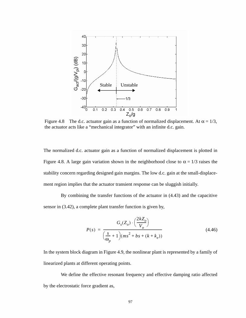
The normalized d.c. actuator gain as a function of normalized displacement is plotted in
Figure 4.8. A large gain variation shown in the neighborhood close to α = 1/3 raises the
stability concern regarding designed gain margins. The low d.c. gain at the small-displace-
ment region implies that the actuator transient response can be sluggish initially.
By combining the transfer functions of the actuator in (4.43) and the capacitive
sensor in (3.42), a complete plant transfer function is given by,
(4.46)
In the system block diagram in Figure 4.9, the nonlinear plant is represented by a family of
linearized plants at different operating points.
We define the effective resonant frequency and effective damping ratio affected
by the electrostatic force gradient as,
Gac
t/(g/
Vpi
) (d
B)
Zo/g
Figure 4.8 The d.c. actuator gain as a function of normalized displacement. At α = 1/3,the actuator acts like a “mechanical integrator” with an infinite d.c. gain.
UnstableStable
P s( )Gs Zo( )
2kZo
Vo------------ ⋅
sωp------ 1+ ms
2bs k ke+( )+ +( )
-------------------------------------------------------------------------=
97

(4.47)
(4.48)
in which and . Substituting (4.47) and (4.48) into (4.46)
yields the plant model in the stable and unstable regimes ( and ),
, stable (4.49)
, unstable (4.50)
4.3.4 Phase-Margin Optimization using a Proportional-Gain Controller
The Nyquist stability criterion indicates that an unstable open-loop with n unsta-
ble poles must have n crossings of the ray (-1 + j0, ) on the Nyquist plot, or the ray:
(φ, r) | φ = , r > 0 dB on the Nichols chart. With one unstable pole, and the num-
C(s)+_F(s)
PlantControllerPre-filter
∆v∆vs2kZo
∆Fe
1
ms2
bs k ke+( )+ +---------------------------------------------- G Zo( )
1 s ωp⁄+----------------------
Vo
∆z
Figure 4.9 The nonlinear plant is replaced by a set of linearized plants at different oper-ating points.
∆vr
ωe1 3α–1 α–
----------------ωn=
ξe1 α–
1 3α–----------------ξ=
ωn k m⁄= ξ b 2 mk( )⁄=
α 1 3⁄≤ α 1 3⁄>
P s( )Gs Zo( )
2Zo
Vo--------- ωn
2
sωp------ 1+ s
22ξeωes ωe
2+ +( )
---------------------------------------------------------------------=
P s( )Gs Zo( )
2Zo
Vo--------- ωn
2
sωp------ 1+ s
22ξeωes ωe
2–+( )
--------------------------------------------------------------------=
∞–
180– °
98

ber of poles is at least two more than the number of zeros, the trajectory must start
from on the Nichols chart (or the Bode plots) to result in a stable system, as shown
in Figure 4.10(a) and (b). The lower gain-margin, GL, and the upper gain-margins, GH, are
defined at frequencies when ∠L(jω) = -180°, and the phase margin, φ, is defined at the
loop unity-gain frequency when |L(jω)| = 1. has a finite lower gain margin as a
result of having an unstable pole, as compared to an infinite lower gain-margin for a stable
open-loop transfer function.
Given a set of linearized unstable plants, we will analyze the maximum attainable
phase margin using a proportional-gain controller, and find the resultant lower and upper
gain-margins, and the minimum crossover frequency accordingly.
4.3.4.1 Plant in the Unstable Regime
By multiplying a proportional-gain controller, C(s) = kp, with the unstable linear-
ized plant in (4.50), the resultant open-loop function is,
(4.51)
where
(4.52)
By using standard complex number arithmetic, magnitude and phase of
are expressed by,
L jω( )
180°–
L jω( )
L s( ) C s( )P s( )=
Ks
ωp------ 1+ s
22ξeωes ωe
2–+( )
--------------------------------------------------------------------=
K Gs Zo( )2Zo
Vo--------- ωn
2kp=
L jω( )
99
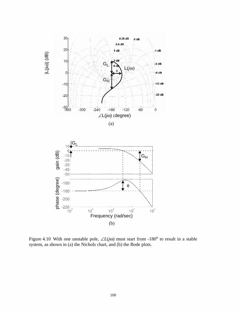
∠L(jω) (degree)
|L(jω
)| (
dB)
Figure 4.10 With one unstable pole, ∠L(jω) must start from -180o to result in a stablesystem, as shown in (a) the Nichols chart, and (b) the Bode plots.
GL
GH
φ L(jω)
φ
GH
GL
Frequency (rad/sec)
gain
(dB
)ph
ase
(deg
ree)
(a)
(b)
100

(4.53)
and
(4.54)
At zero frequency ( ), and (4.53) becomes,
(4.55)
Substituting (4.55) into (4.53), and equating (4.53) to unity at the crossover frequency, ωc,
yields
(4.56)
From (4.55) and (4.56), we have,
(4.57)
in which r1 = ωc/ωe and r2 = ωp/ωe. For stability consideration, must be larger than
one (0 dB), thus the following inequality must hold,
(4.58)
Equating to at the upper gain-margin frequency, ωg, gives,
(4.59)
Substituting (4.59) into (4.53) gives the upper gain margin,
L jω( ) K
1 ω2 ωp2⁄+ ω2 ωe
2+( )2 2ξeωeω( )2+------------------------------------------------------------------------------------------------=
L∠ jω( ) π–2ξeωeωω2 ωe
2+------------------- tan-1 ω
ωp------ tan-1–+=
L j0( ) GL=
GLKωe
2------=
GL
ωp2 ωc
2+ ωc2 ωe
2+( )2 2ξeωeωc( )2+
ωpωe2
--------------------------------------------------------------------------------------------=
Kr1
2 r22+ r1
2 1+( )2 2ξer1( )2+
r2--------------------------------------------------------------------------
ωe2⋅=
GL
ωp2 ωc
2+( ) ωc2 ωe
2+( )2 2ξeωe( )2+( ) ωp2ωe
4>
L jω( )∠ π–
ωg ωe 2ξeωp ωe–( )=
101

(4.60)
must be larger than unity for stability consideration. At ω = ωc, the phase angle of
in (4.54) gives,
(4.61)
(4.62)
To get the maximum phase margin, (4.54) is differentiated with respect to at .
The resultant crossover frequency is the solution of the following 4th-order equation:
(4.63)
At each operating point, and are first computed according to (4.47) and
(4.48). Given the ωp/ωe ratio and , is found from (4.63). Then the maximum phase
margin, the upper and lower gain-margins and the controller gain are solved from (4.62),
(4.60), (4.56), and (4.52), respectively, at each operating point. The optimal controller gain
which gives the maximum phase margin varies with the displacement, implying that the
optimal controller must be linear time-varying (LTV) in order to secure the maximum
phase margins at all displacements. We implement a linear time-invariant (LTI) controller
whose gain is selected among the kp’s obtained at all operating points while giving reason-
GH
2ξeωp 1 2ξeωe ωp⁄ ωe2 ωp
2⁄–+( )GLωe
-------------------------------------------------------------------------------=
GH
L jω( )
π– φ+ π–2ξeωeωc
ωc2 ωe
2+--------------------- tan-1 ωc
ωp------ tan-1–+=
φ
2ξeωeωφ
ωφ2 ωe
2+----------------------
ωφωp------–
12ξeωeωφ
ωφ2 ωe
2+----------------------
ωφωp------⋅+
-------------------------------------------
tan-1=
ω ω ωc=
ωp– 2ξeωe–( )ωc4 2ξeωp
2ωe– 2ωpωe2– 4ξe
2ωpωe2– 2ξeωe
3+( )ωc2
2ξeωp2ωe
3 ωpωe4–( )+ +
0=
ωe ξe
ξe ωc
102

able phase and gain margins for all displacements. A complete LTI controller design flow
is depicted in Figure 4.11.
Using the plant parameters given in Chapter 3 with an initial gap of 3 µm, we
plot the maximum phase margin, the corresponding lower and upper gain margins, the
crossover frequency, and the controller gain from Figure 4.12(a) to Figure 4.12(e). The
phase margin at large displacements is over due to the large damping ratios at small
gaps. The selected LTI controller is kp = 16 which gives all the operating points a mini-
mum phase margin of . The effective damping ratio and the effective resonant fre-
quency are plotted as a function of normalized displacement in Figure 4.13(a) and (b),
respectively. The resultant open-loop transfer functions of LTV and LTI designs are plot-
ted on the Nichols chart in Figure 4.14(a) and (b) for selected normalized displacements.
4.3.4.2 Plant in the Stable Regime
By multiplying a proportional-gain controller, , with the stable linear-
ized plant in (4.49), the open-loop function below the pull-in limit is,
(4.64)
Without unstable poles, the phase of starts from for or for
, thereby the lower gain margin does not exist.
Equating of (4.64) to at the gain-margin frequency, , gives,
(4.65)
60°
60°
C s( ) kp=
L s( ) C s( )P s( )=
Ks
ωp------ 1+ s
22ξeωes ωe
2+ +( )
---------------------------------------------------------------------=
L jω( ) 0° α 1 3⁄< 90°–
α 1 3⁄=
L jω( )∠ π– ωg
ωg ωe 2ξeωp ωe+( )=
103

Compute from
(4.47)
ωe i,
Compute from
(4.53)
ωc i,
Compute , , ,
and , from (4.62),
(4.60), (4.56), and (4.52)
φi GH i, GL i,
kp i,
i = 1 to n
Zo,i = g/3 + i ∆z⋅
, ξe i,ωp
ωe------
ωe i,
ωc i,
Select kp among all kp,i’s
Figure 4.11 Flow chart for LTI proportional-gain controller design for a set of linearizedunstable plants. Final controller design kp must ensure adequate phase and gain marginsfor all the linearized plants.
104

low
er g
ain
mar
gin
GL
(dB
)
uppe
r ga
in m
argi
n G
H (
dB)
phas
e m
argi
n (d
egre
e)
Zo/g
Zo/g
Zo/g
(a)
(c)
(b)
(d)
Figure 4.12 Maximum phase margin, andcorresponding crossover frequency, lowergain margin, upper gain margin and control-ler gain plotted as a function of normalizeddisplacement from (a) to (e). Selected LTIcontroller is kp = 16 which gives a minimum
phase margin around 60o at all displace-ments.
(e)
Zo/g
Zo/g
k pωc/
ωn
105

Figure 4.13 (a) Effective damping ratio as a function of normalized displacement. (b)Ratio of effective resonant frequency over mechanical resonant frequency as a function ofnormalized displacement.
Zo/g
Zo/g
(a)
(b)
effe
ctiv
e da
mpi
ng r
atio
, ξe
ωe/ω
n
106

Figure 4.14 (a) Open-loop transfer function of LTV design on the Nichols chart. (b)Open-loop transfer function of LTI design on the Nichols chart.
phase (degree)(a)
(b)
phase (degree)
open
-loop
mag
nitu
de (
dB)
open
-loop
mag
nitu
de (
dB)
α = 0.34 0.87 0.73 0.40 0.53 0.60
α = 0.34 0.40 0.87 0.73 0.53 0.60
107

Substituting (4.65) into (4.64) gives,
(4.66)
For stability consideration, must be larger than unity (0 dB). Thus the following ine-
quality sets the upper controller gain limit:
(4.67)
Substituting the plant parameters given in Chapter 3 for plate displacement up to one-third
of the gap (g = 3 µm), we plot the maximum stable controller gain as a function of normal-
ized displacement in Figure 4.15. The kp values are at least an order of magnitude larger
than kp values obtained in the unstable regime as shown in Figure 4.12(e). Hence there is
no conflict in the designed controller gain in the stable and unstable regimes.
GH
2ξeωe ωp2
2ξeωeωp ωe2
+ +( )Kωp
--------------------------------------------------------------------=
GH
kp
Vo
G Zo( )Zo---------------------
ξeωe ωp2 2ξeωeωp ωe
2+ +( )ωpωn
2-----------------------------------------------------------------⋅<
1/9 2/9 1/3Zo/g
Figure 4.15 Maximum controller gain kp versus normalized plate displacement by stabil-ity requirement.
k p
108

4.3.5 Plant Input Disturbance Rejection
Using linearization, we neglect the initial conditions of plate and the high-order
terms of electrostatic force which are important to the nonlinear system stability. These
effects are modelled as plant input disturbances in this section. We perform disturbance
rejection to reduce the induced plate displacement due to disturbances, thereby increasing
the stability robustness of the system.
4.3.5.1 Problem Formulation
By linearization, only the first-order terms of the expanded nonlinear electro-
static force in the Taylor’s series are considered as in (4.41). The sum of the remaining
high-order terms, denoted as ∆Fd, at operation point ( ) is given by,
(4.68)
where ∆Fd,z, ∆Fd,zv, and ∆Fd,v are the small-signal disturbance forces with respect to ∆z,
∆z and ∆v, and ∆v, respectively. Substituting the electrostatic force expression of (2.16)
into (4.68), we can represent ∆Fd,z, ∆Fd,zv, and ∆Fd,v as the multiple of the spring restoring
force at as the following:
(4.69)
(4.70)
Zo Vo,
∆Fdz
i
i
∂
∂ Fe
Zo Vo,
∆zi
zi
i
∂
∂ Fe
vj
j
∂
∂ Fe
j 1=
∞
∑Zo Vo,
∆zi∆v
j
vi
i
∂
∂ Fe
Zo Vo,
∆vi
i 2=
∞
∑+
i 1=
∞
∑+
i 2=
∞
∑=
∆Fd z, ∆Fd zv, ∆Fd v,+ +=
z Zo=
∆Fd z,n 1+( ) αrz( )n
1 α–( )n---------------------------------
n 2=
∞
∑
kZo⋅=
∆Fd zv,2rv αrz( )n 1–
1 α–( )n 1–------------------------------
2rv2 αrz( )n 1–
n 1+( ) 1 α–( )n 1–--------------------------------------------
n 2=
∞
∑+
n 2=
∞
∑
kZo⋅=
109

(4.71)
where rz = ∆z/Zo and rv = ∆v/Vo.
∆Fd,z is the dominant disturbance force at small gaps. The ratio of ∆Fd,z over the
first-order electrostatic force, ∆Fe,1, as a function of normalized displacement is shown in
Figure 4.16, which illustrates that ∆Fd,z dominates over the first-order term for Zo/g > 0.8
and ∆z/Zo > 0.075. Therefore performing disturbance rejection in this region is especially
important.
The block diagram with the input disturbance force is shown in Figure 4.17, in
which the voltage-to-force gain of 2kZo/Vo in the original plant is included within the rede-
fined controller, C’(s) = C(s)⋅2kZo/Vo, and the plant is redefined as P’(s) = P(s)/(2kZo/Vo).
The aforementioned linear stability analysis assumes that the motion trajectory
exactly follows the steady-state displacement and applied voltage, yet deviations exist due
∆Fd v, rv2kZo=
Figure 4.16 Ratio of disturbance force over first-order electrostatic force plotted as afunction of normalized displacement for ∆z/Zo = 0.025 to 0.1.
Zo/g
∆Fd,
z/∆F
e,1
110

to the quasi-static operation, as shown by the elliptical disc with radii ∆z and ∆v on the
static displacement-voltage plot in Figure 4.18. The implication of performing disturbance
rejection with respect to the perturbed displacement and voltage and their induced distur-
bance force, , is to suppress the final perturbed displacement as shown in Figure
4.17. Therefore the quasi-static trajectory is brought closer to the neighborhood of linear-
ized operating point through disturbance rejection.
4.3.5.2 Controller Design
Graphically speaking, as shown in Figure 4.19, the operating point is
said to be asymptotically stable if for such that for , then
for . The final destination would be biased from Zo by under
the plant input disturbance, shown as the point on the same plot. By performing dis-
turbance rejection with a large loop transmission gain at low frequencies, asymptotically
stable operation can be achieved with .
C(s)+_F(s)
P’(s)C’(s)Pre-filter
∆Fd
1
ms2
bs k ke+( )+ +---------------------------------------------- G Zo( )
1 s ωp⁄+----------------------
Figure 4.17 High-order terms of the electrostatic force expanded by the Taylor’s seriesare formulated as an input disturbance force.
∆z∆v ∆vs
2kZo
Vo
∆Fd ∆ z
z Zo=
∆z 0> z to( ) ∆z<
z to t+( ) Zo→ t ∞→ ∆z
Z′o
Z′o Zo≅
111
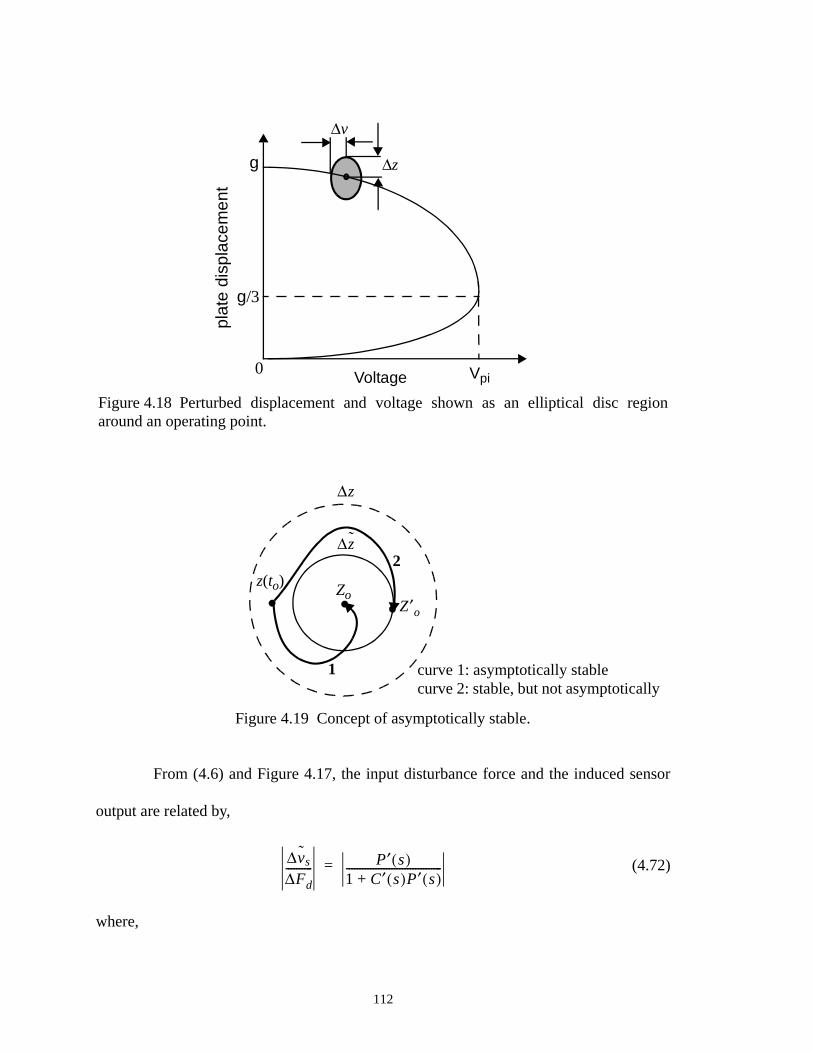
From (4.6) and Figure 4.17, the input disturbance force and the induced sensor
output are related by,
(4.72)
where,
∆z
∆v
Voltage Vpi
plat
e di
spla
cem
ent
g/3
g
0
Figure 4.18 Perturbed displacement and voltage shown as an elliptical disc regionaround an operating point.
Zo
∆z
∆z2
1
Figure 4.19 Concept of asymptotically stable.
z(to)
curve 1: asymptotically stablecurve 2: stable, but not asymptotically
Z′o
∆vs
∆Fd---------- P′ s( )
1 C′ s( )P′ s( )+------------------------------------=
112

(4.73)
(4.74)
Assume that at low frequencies, we substitute , (4.73) and
(4.74) into (4.72), producing the steady-state displacement, , expressed by,
(4.75)
Hence, required is given by,
(4.76)
∆Fd is calculated at each normalized displacement by substituting the perturbed
displacement ratio, = 0.075, and from Figure 4.6(a) (ωb/ωn = 0.05)
through (4.69) to (4.71). By substituting the plant parameters given in Chapter 3, the ∆Fd
values, and the resultant displacement ratio, = 0.01, into (4.76), the required con-
troller gain for disturbance rejection is plotted as a function of normalized displacement in
Figure 4.20. Also shown in the plot are the optimal LTV design from Figure 4.12(e), and
the maximum LTI controller gain kp = 220 to maintain marginal system stability (phase
margin = 0°). The controller gain increases below Zo/g < 0.2 and beyond Zo/g > 0.8 due to
the large ∆Fd values resulting from large ∆v/Vo and ∆z/Zo, respectively. The required con-
C′ s( )2kkpZo
Vo-----------------=
P′ s( )Gs Zo( )
ms2
bs k ke+( )+ +( ) 1 s ωp⁄+( )-------------------------------------------------------------------------------=
C′P′ 1» ∆ vs ∆zGs Zo( )=
∆z
∆z∆Fd----------
P′ 0( )C′ 0( ) P′ 0( )----------------------------------=
Vo
2kkpZoGs Zo( )-----------------------------------=
kp
kp
Vo∆Fd
2kZoGs Zo( )∆ z------------------------------------=
∆z Zo⁄ ∆v Vo⁄
∆z Zo⁄
113
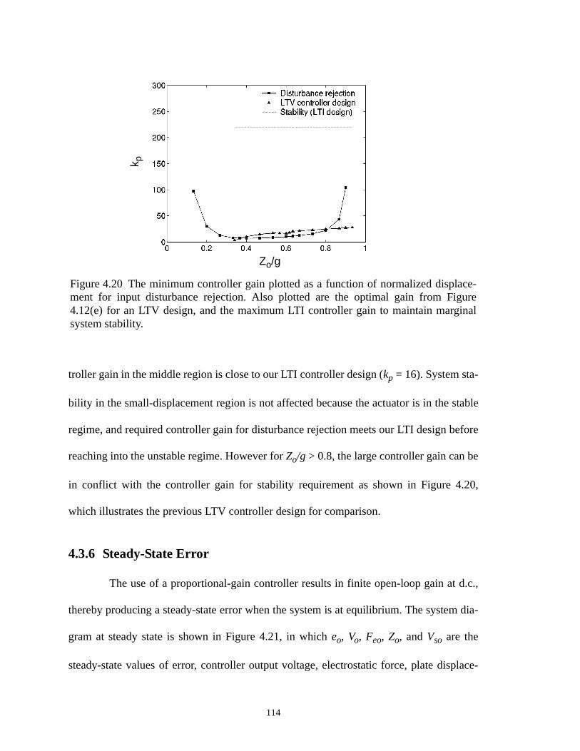
troller gain in the middle region is close to our LTI controller design (kp = 16). System sta-
bility in the small-displacement region is not affected because the actuator is in the stable
regime, and required controller gain for disturbance rejection meets our LTI design before
reaching into the unstable regime. However for Zo/g > 0.8, the large controller gain can be
in conflict with the controller gain for stability requirement as shown in Figure 4.20,
which illustrates the previous LTV controller design for comparison.
4.3.6 Steady-State Error
The use of a proportional-gain controller results in finite open-loop gain at d.c.,
thereby producing a steady-state error when the system is at equilibrium. The system dia-
gram at steady state is shown in Figure 4.21, in which eo, Vo, Feo, Zo, and Vso are the
steady-state values of error, controller output voltage, electrostatic force, plate displace-
k p
Figure 4.20 The minimum controller gain plotted as a function of normalized displace-ment for input disturbance rejection. Also plotted are the optimal gain from Figure4.12(e) for an LTV design, and the maximum LTI controller gain to maintain marginalsystem stability.
Zo/g
114

ment, and sensed voltage. The voltage-to-force gain, f(Zo), is a function of displacement
given by,
(4.77)
and the large-signal sensor gain at steady state is,
(4.78)
Multiplying all the gains within the loop gives the total d.c. loop gain at z = Zo as,
(4.79)
The steady-state error is related to the input-command magnitude, r, by,
(4.80)
By substituting (4.79) into (4.80), and assuming that , (4.80) becomes,
(4.81)
f Zo( )2εoAkZo
2 g Zo–( )-------------------------=
Gso Zo( ) Vso Zo⁄=
L j0( ) z Zo=
kpf Zo( )Go Zo( )k
------------------------------------=
kpVso
2k g Zo–( )--------------------------
2εoAk
Zo---------------=
+_Feo
Gso(Zo)1k
f(Zo)Vo Zoeo
kp
r
ControllerActuator
Sensor
Figure 4.21 System block diagram at equilibrium point z = Zo.
Vso
eo
r----- 1
1 L j0( ) z Zo=+-------------------------------------=
L j0( )z Zo=
1»
eo
r-----
2k g Zo–( )kpVso
--------------------------Zo
2εoAk---------------≅
115
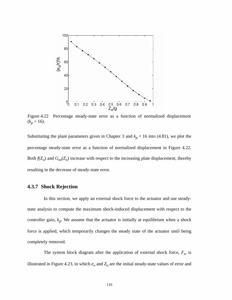
Substituting the plant parameters given in Chapter 3 and kp = 16 into (4.81), we plot the
percentage steady-state error as a function of normalized displacement in Figure 4.22.
Both f(Zo) and Gso(Zo) increase with respect to the increasing plate displacement, thereby
resulting in the decrease of steady-state error.
4.3.7 Shock Rejection
In this section, we apply an external shock force to the actuator and use steady-
state analysis to compute the maximum shock-induced displacement with respect to the
controller gain, kp. We assume that the actuator is initially at equilibrium when a shock
force is applied, which temporarily changes the steady state of the actuator until being
completely removed.
The system block diagram after the application of external shock force, Fs, is
illustrated in Figure 4.23, in which eo and Zo are the initial steady-state values of error and
Figure 4.22 Percentage steady-state error as a function of normalized displacement(kp = 16).
(eo/
r)%
Zo/g
116

plate displacement, ∆es and ∆zs are the changes of steady-state error and steady-state dis-
placement, and Vo’, Feo’, and Vso’ are the new steady-state values of controller output volt-
age, electrostatic force, and sensed voltage. By solving the balanced electrostatic force,
spring restoring force, and shock force, the voltage-to-force function, f ’, is given by,
(4.82)
The open-loop functions before and after the application of shock force are
defined as L and L’, respectively. From Figure 4.22 and Figure 4.23, the change of the sen-
sor output is given by,
(4.83)
Define
(4.84)
and
f′2εoA k Zo ∆zs+( ) Fs–( )
2 g Zo ∆zs+( )–( )-------------------------------------------------------------=
+_Feo’
Gso’(Zo+∆zs)1k
f’(Zo+∆zs)
Vo’eo+∆es
kp
rZo+∆zs
Fs (shock)
Figure 4.23 System block diagram at a new equilibrium point z = Zo + ∆zs due to theexternal shock force applied to the actuator.
C’ P’
Vso’
Vso' Vso–L′r
1 L′+--------------
P′Fs
1 L′+--------------+
Lr1 L+------------–=
L′1 L′+-------------- L
1 L+------------–
rP′Fs
1 L′+--------------+=
ψf Gso Zo( )⋅
k--------------------------≡
117
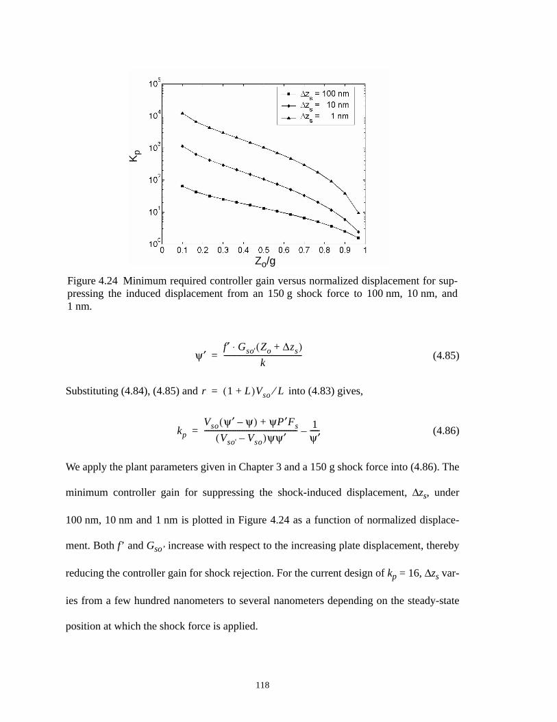
(4.85)
Substituting (4.84), (4.85) and into (4.83) gives,
(4.86)
We apply the plant parameters given in Chapter 3 and a 150 g shock force into (4.86). The
minimum controller gain for suppressing the shock-induced displacement, ∆zs, under
100 nm, 10 nm and 1 nm is plotted in Figure 4.24 as a function of normalized displace-
ment. Both f’ and Gso’ increase with respect to the increasing plate displacement, thereby
reducing the controller gain for shock rejection. For the current design of kp = 16, ∆zs var-
ies from a few hundred nanometers to several nanometers depending on the steady-state
position at which the shock force is applied.
ψ′f′ Gso' Zo ∆zs+( )⋅
k-------------------------------------------=
r 1 L+( )Vso L⁄=
kp
Vso ψ′ ψ–( ) ψP′Fs+
Vso' Vso–( )ψψ′--------------------------------------------------- 1
ψ′-----–=
Figure 4.24 Minimum required controller gain versus normalized displacement for sup-pressing the induced displacement from an 150 g shock force to 100 nm, 10 nm, and1 nm.
Zo/g
Kp
118

4.4 Controller Design by the QFT (Quantitative Feedback Theory) Method
The frequency-domain design procedure discussed in Section 4.3 only deals with
a nominal nonlinear plant, whose parameters can be uncertain within a range instead of
being a fixed value. For example, the initial gap can vary between 2 to 3 µm due to the
variation of actuator curl. To design efficiently with plant uncertainties, the previous
approach is inappropriate for its lack of robustness consideration, which is why the QFT
method is presented in this section.
The QFT is a frequency-domain design method developed by Horowitz [81]
based on two important observation of feedback systems: (1) the use of feedback is to
achieved a desired plant output response in the presence of plant uncertainty, and/or
unknown external disturbances; and (2) controller design with the least required band-
width is preferred. The canonical QFT system configuration is the two degree-of-freedom
diagram shown in Figure 4.5. We modify the design procedure given in [81] for use in our
design problem. The design steps are:
(1) Design of the pre-filter based on the desired tracking bandwidth as discussed in Sec-
tion 4.3.2.
(2) Derivation of templates of the uncertain linearized plants on the complex plane (the
Nichols chart) at frequencies (i = 1, 2,...,n).
(3) Selection of a nominal plant, Po(s), among all linearized plants, and derivation of
bounds on the nominal open-loop function, Lo(jω), at ω = ωi based on stability and
disturbance-rejection specifications.
(4) Design Lo(jω) based on bounds at .
ωi
ω ωi=
119

4.4.1 Generation of Bounds
The essence of the QFT method is the transformation of robust stability and
robust performance specifications into domains on the complex plane (the Nichols chart),
referred to as bounds, which a nominal loop transmission should obey in design. The spec-
ifications considered in our design include:
(1) Gain and phase margins:
(4.87)
(2) Plant input disturbance rejection:
(4.88)
The lower gain margin and phase margin are related to by [82],
, (4.89)
and
- cos-1 (4.90)
For example, = 1.2 implies at least phase margin and at least 1.66 (4.4 dB) upper
gain margin.
To derive bounds for stability margins, we represent the controller and plant
transfer functions in their polar form: and , and substitute them into
(4.87),
(4.91)
Evaluating the magnitude and squaring both sides yields a second-order inequality,
T jω( ) λ≤
P jω( )S jω( ) w1 ω( )≤
λ
GL 11λ---+=
φ 180°=1
2λ2--------- 1–
λ 50°
C cejϕ
= P pejθ
=
cpej ϕ θ+( )
1 cpej ϕ θ+( )
+------------------------------------ λ≤
120

(4.92)
Similarly, the input-disturbance rejection specification in (4.88) gives the inequality,
(4.93)
Following the procedure described in [82], as illustrated in the flow chart in Figure 4.25,
the bounds for the nominal loop transmission are obtained. The final controller
design is not affected by the selected nominal plant. Graphically speaking, the bound com-
puted at each frequency is categorized into two types as depicted on the Nichols chart in
Figure 4.26. The area indicated by arrows is where the nominal loop transmission must
fall within if given one of them, to satisfy the inequalities (4.92) and (4.93).
The uncertain plant that we consider has a gap variation between 2 to 3 µm. The
gap is discretized by n points as,
(4.94)
We set n = 3, gmin = 2 µm, and gmax = 3 µm. At each gi, the nonlinear plant is linearized at
a total of m positions, aij (j = 1 to m), equally spaced by
, where α is the normalized displacement. We set m = 5.
The total number of linearized plants used for bound generation is n×m = 15. The three
discrete gaps are g1 = 2 µm, g2 = 2.5 µm, and g3 = 3 µm, with the minimum and maxi-
mum αi’s given by: , ,
and . The nominal plant is chosen with g = g3, and
α = α31 = 0.34. we substitute into (4.89) and (4.90) to get a minimum phase
p2
11
λ2-----–
c2
2p ϕ θ+( )cos[ ]c 1 0≥+ +
p2g
22p ϕ θ+( )cos[ ]g 1
p2
w12 ω( )
---------------–
0≥+ +
Lo jω( )
g gi i 1 … n, ,=, gi gmin gmax,[ ]∈,=
∆αi αi max, αi min,–( )= m 1–( )⁄
α1 min, α1 max,,[ ] 0.34 0.85,[ ]= α2 min, α2 max,,[ ] 0.34 0.88,[ ]=
α3 min, α3 max,,[ ] 0.34 0.90,[ ]=
λ 1.3=
121

Figure 4.25 Flow chart for computing QFT bounds [82].
1.Discretize frequency w into a finite set: = wi| i = 1,..., n.Ω
2.Select a nominal plant ,
.
Po s( ) ℘∈ P1 s( ) … Pm s( ), , =
Po jω( ) poejθo=
3.Define a phase range , and dis-
cretize it for the controller phase .
Φϕl
4.Choose a single frequency .ω Ω∈
5.Choose a single controller’s phase .ϕi Φ∈
6.Choose a single plant .Pk s( ) ℘∈
7.Compute and
using (4.92) and (4.93).
gmax Pk( )
gmin Pk( )
8.Set
and .
gmax ϕ( ) max gmax Pk( )[ ]=
gmin ϕ( ) min gmin Pk( )[ ]=
9.Set
and ,
.
Lo max, ψo( ) pogmax ϕ( )=
Lo min, ψo( ) pogmin ϕ( )=
ψo ϕ θo+=
k = 1 to m
i = 1 to n
j = 1 to l
122

margin and an upper gain margin of and 4.95 dB. At selected frequencies = 10,
1000, 10000, 50000, 100000, and 500000, the magnitude and phase of the linearized plant
templates are plotted on the Nichols chart shown in Figure 4.27(a). The generated stability
bounds and the stability line for the nominal unstable plant is illustrated on the Nichols
chart in Figure 4.27(b).
4.4.2 Modification of Bounds and Loop Shaping
For loop-shaping with an unstable and/or non-minimum phase nominal plant, the
bounds must be shifted to convert the loop-shaping problem to that for a stable minimum
phase nominal plant [83][84]. The reason is that it is more convenient to work with a min-
imum phase function in numerical design because the Bode integral can be used, and the
optimal loop shaping can be derived [81].
Given a uncertain unstable/non-minimum-phase plant,
45° ω
OK
OK
Figure 4.26 Typical QFT bounds displayed on the Nichols chart for design of the looptransmission Lo(jw). (type I: line. Type II: closed contour.)
Type I
Type II
∠L(jω) (degree)
|L(jω
)| (
dB)
123
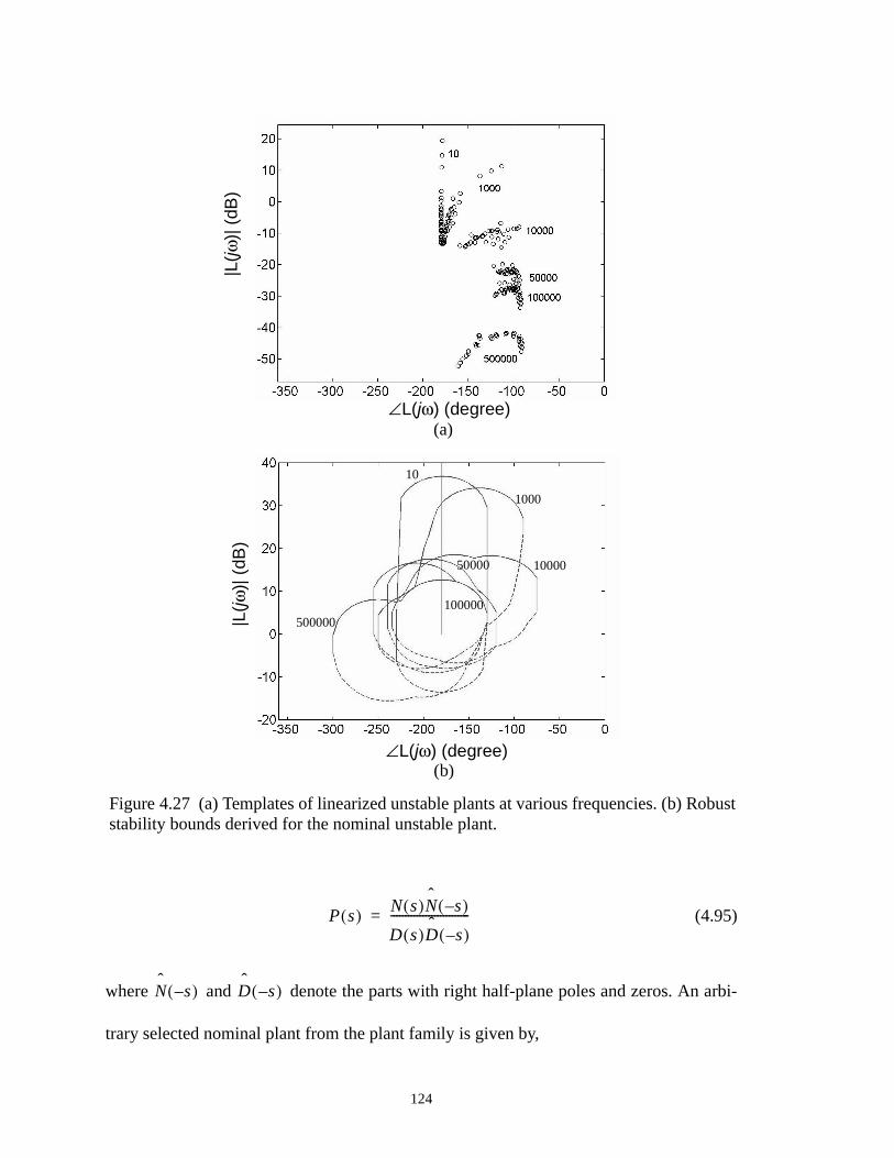
(4.95)
where and denote the parts with right half-plane poles and zeros. An arbi-
trary selected nominal plant from the plant family is given by,
10
1000
1000050000
100000500000
(a)
(b)
Figure 4.27 (a) Templates of linearized unstable plants at various frequencies. (b) Robuststability bounds derived for the nominal unstable plant.
|L(jω
)| (
dB)
|L(jω
)| (
dB)
∠L(jω) (degree)
∠L(jω) (degree)
P s( ) N s( )Nˆ
s–( )
D s( )Dˆ
s–( )---------------------------=
Nˆ
s–( ) Dˆ
s–( )
124

(4.96)
We define an all-pass filter containing the right-half plane poles and zeros as,
(4.97)
which relates the new nominal stable/minimum-phase plant to the original nominal plant
by,
(4.98)
Thus the loop transmission is related to the new loop transmission by,
(4.99)
The bounds imposing on are the same in magnitude as the bounds imposing on
yet with a horizontal phase shift of [83]. In addition, the stability line defined
on the Nyquist plot and the Nichols chart in Section 4.2.2.1 becomes,
(4.100)
and
, (4.101)
Po s( )No s( )N
ˆo s–( )
Do s( )Dˆ
o s–( )--------------------------------=
A s( ) Nˆ
o s–( )Dˆ
o s( )
Nˆ
o s( )Dˆ
o s–( )-------------------------------=
Po' s( ) Po s( )A s( ) 1–=
L s( ) L' s( )
L s( ) C s( )P s( ) C s( )P' s( )A s( ) L' s( )A s( )= = =
L' s( ) L s( )
A jω( )∠–
R'o ω( ) x y,( )x k 1+( ) A jω( )–( )∠( )y k 1+( ) A jω( )–( )∠( )k 0>
,sin–=,cos–=
=
R'1 ω( ) φ r,( )φ 2q 1+( )180°– A
1–jω( )
r 0
q 1 2 …,±,±=
,>,∠+=
=
125

respectively, as shown in Figure 4.28. Due to the shift of those stability lines, the stability
criterion is modified as given in Theorem 4.3 [84].
Theorem 4.3 For the plant with n right half plane poles, the closed-loop system is stable
if and only if as defined in (4.99) does not intersect the point at the same
frequency , and the net number of positive and negative crossings on the stability line
at the same frequency is n.
The nominal unstable plant is modified to a nominal stable plant using (4.98).
The final bounds, including the stability lines, after being shifted by , are shown
in Figure 4.29.
The loop shaping of Lo′(jω) is in Figure 4.30, which shows that derived bounds
are not violated by Lo′(jω) at ω = ωi, indicating that the desired phase margin and upper
gain margin are satisfied by design. The designed proportional-gain controller is ,
-1 real
imagR'1 ω1( ) R'1 ω2( ) R'1 ω3( )
R'o ω1( )
R'o ω2( )
R'o ω3( )
Figure 4.28 New stability lines on the Nyquist plot (left) and the Nichols chart (right),derived for unstable and/or nonminimum phase plants [84].
∠L(jω) (degree)|L
(jω)|
(dB
)
L' jω( ) A jω( )–
ω
R'1 ω( )
A1–∠ jω( )
kp 30=
126

which is larger than previous design (kp = 16) for a single nonlinear plant in Section 4.3,
because additional gain-bandwidth must be paid for sensitivity reduction of plant uncer-
tainties (g = 2 to 3 µm instead of 3 µm only).
ω = 10 rad/s1000
10000
50000100000
500000
Figure 4.29 Robust stability bounds and stability lines derived for the new stable nominalplant.
∠L(jω) (degree)
|L(jω
)| (
dB)
10
1000
1000050000100000
500000
ω = 500000
L’o(jω)
ω = 10 rad/sω = 1000
ω = 10000
ω = 50000
ω = 100000
Figure 4.30 Shaping of nominal open-loop function based on the derived bounds, suchthat Lo’(jω) does not fall within the area as indicated in Figure 4.26. (kp = 30)
∠L(jω) (degree)
|L(jω
)| (
dB)
127

4.4.3 Plant Input Disturbance Rejection
For plant input-disturbance rejection, the plant templates and bound generation
are constructed point-by-point for a total of n×m times. The final bounds, BD, are the inter-
section of the total n×m bounds. Each set of bounds Bd,ij is scaled by the ratio, 2kZo,ij/Vo,ij,
over that of the selected nominal plant, , so all the bounds are referred as
for the nominal plant. and are the operating displacement and the operat-
ing voltage of the nominal plant selected at g = g3, and α = α35 = 0.9. and are
the operating displacement and the operating voltage of the other plants. The final bounds
are given by,
(4.102)
We substitute and into (4.69) to (4.71), and obtain the disturbance
force, Fd,ij, at all displacements, , as multiples of the spring restoring force, .
We set the ratio, , of the final perturbed displacement over the steady-state dis-
placement to 0.01. Substituting the capacitive sensor gain given by (3.43) into (4.75)
yields the sensitivity-reduction specification,
(4.103)
2kZo iojo, Vo iojo,⁄
Zo iojo, Vo iojo,
Zo ij, Vo ij,
BD
Bd ij,2kZo ij, Vo ij,⁄
2kZo iojo, Vo iojo,⁄--------------------------------------- --------------------------------------------
j 1=
m
∩i 1=
n
∩=
Bd ij, Vo ij, Zo iojo,
Vo iojo, Zo ij,-------------------------------------
j 1=
m
∩i 1=
n
∩=
rv 0.1= rz 0.075=
αij DijkZo ij,
∆ zij Zo ij,⁄
∆vs ij,Fd ij,-------------
G Zo ij,( )∆zij
DijkZo ij,------------------------------=
128

where is the final perturbed sensed voltage. The final bounds on the Nichols chart
are illustrated in Figure 4.31 for frequencies up to 100,000 rad/sec. Also shown is the
nominal loop-shaping using a minimum controller gain, kp = 106 to satisfy the bounds.
This large kp is similar to previous results in Figure 4.20.
4.5 Scaling of Plant Parameters
Control design procedures for a given fixed plant and a given plant with initial
gap variation have been introduced in Section 4.3 and 4.4. As design guidance for both
plant and controller, it will be beneficial to understand how the scaling of plant parame-
ters, such as mass, spring, and plate area, affects the controller design, in order to provide
directions for achieving a good plant design. A good plant design for parallel-plate servo
should help to reduce the cost of feedback, namely, the open-loop bandwidth, in dealing
with the unstable pole after the pull-in limit. Implemented gain-bandwidth product of the
servo and sensing circuits can therefore be smaller to reduce power consumption.
∆vs ij,
Figure 4.31 Input-disturbance bounds and loop-shaping result using kp = 106.
phase (degree)
mag
nitu
de (
dB)
Lo(jω)
11000
10000
100000
ω = 1 rad/secω = 1000
ω = 10000
ω = 100000
129

The rule of thumb discussed in Section 4.2.2.2 and 4.2.2.4 states that the open-
loop unity-gain frequency should be at least twice the unstable pole frequency in order to
achieve a 60° phase margin. By making the unstable pole close to the origin on the com-
plex plane, the resulting open-loop unity-gain frequency is reduced, and so is the circuit
gain-bandwidth product required to be implemented. Implemented circuits within the
feedback loop include the controller, pre-amp, demodulator, and subtracter. The linearized
actuator d.c. gain ranges from 10-6 to 10-7 (unit = m/V), and the capacitive sensor gain is
in the range of 10-4 (unit = V/m). Implemented d.c. voltage gain of control and sensing
circuits can be in the range of a few hundreds to several thousands. If the open-loop unity-
gain frequency is 20 kHz and the d.c. circuit gain is 1000, for example, then the total cir-
cuit gain-bandwidth product should be at least 20 MHz to ensure that the dominant pole
from circuits does not affect phase margin at the open-loop unity-gain frequency.
From (4.47), (4.48), and (4.50), the right-half-plane unstable pole is given by,
(4.104)
To reduce the unstable pole frequency, the damping ratio ξ can be increased and/or the
actuator resonant frequency can be decreased (i.e., decrease of spring constant and/or
increase of mass). Rise time of the output response will increase due to the use of either
approach. Increase of damping ratio is preferred at larger displacements when the spring-
softening effect is more significant. However the rise time can be negatively impacted
with a large damping ratio at small displacements. Assume that the increase of plate area,
A, is proportional to the increase of mass, total linearized d.c. gain of the parallel-plate
actuator and the capacitive sensor is proportional to:
ωrhp ξ2 3α 1–1 α–
----------------+ ξ– ωn=
130

(4.105)
according to (4.45), (3.8), and (3.43). The implemented circuit gain-bandwidth product
can therefore be reduced by A3/2 if the open-loop gain remains the same. An easy way to
reduce the gain-bandwidth product without involving actuator design is to use a large
modulation voltage Vm to improve the capacitive sensitivity. The drawback is that Vm con-
tributes an effective d.c. actuation voltage which limits the maximum controlled displace-
ment. Also, there is a capacitive feedthrough issue in which carrier-frequency signals
sitting on the actuation voltage pass to the sensing plates, and are demodulated back to a
d.c. sensed voltage which eventually adds to the actuation voltage. More discussion of
capacitive feedthrough will be presented in Chapter 5.
Phase margin is negatively impacted by the reduction of damping ratio because
of the increase of unstable pole frequency. By using the plant parameters given in Chapter
3 except a fixed damping ratio (ξ = 0.3 to 1.5) is used for all displacements, an optimal
time-varying proportional-gain controller is designed with the resulting phase margin, the
corresponding lower and upper gain margins, the crossover frequency, and the controller
gain shown from Figure 4.32(a) to (e). Phase margin decreases monotonically with
increasing displacement due to the use of a fixed damping ratio for all displacements.
Damping in air is not fixed, however these plots show the trend for decreasing damping.
The system can not be stabilized over the entire gap at underdamped and slightly over-
damped situations unless phase-lead compensation is employed. Although phase margin
can be attained with phase-lead compensation, the resultant large open-loop bandwidth
GactGs1
Vpi------- A⋅∝
A3 2⁄
=
131

Zo/g Zo/g
Zo/gZo/g
Zo/g
k pup
per
gain
mar
gin,
GH
(dB
)
low
er g
ain
mar
gin,
GL
(dB
)ph
ase
mar
gin
(deg
ree)
Figure 4.32 Maximum phase margin, andcorresponding crossover frequency, lowergain margin, upper gain margin and con-troller gain plotted as a function of nor-malized displacement from (a) to (e).
ωc/
ωn
(a)
(b)
(c)
(d)
(e)
0.3
0.60.91.21.5
132

includes more sensor noise, and the disturbance in the expanded bandwidth is likely to
excite the higher mechanical modes.
To summarize, the scaling of plant parameter should be directed towards the
reduction of cost of feedback, and thereby the implemented gain-bandwidth product of
control and sensing circuits. Gain of the circuits can be reduced with increasing actuator
gain and capacitive sensor gain resulting from a larger actuation/sensing plate area. Band-
width of the circuits can be reduced by decreasing the unstable pole frequency resulting
from a larger damping ratio and/or a smaller mechanical bandwidth.
133

134

Chapter 5
Experimental Results
5.1 Introduction
In this section, we present the experimental results on plant characterization and
closed-loop feedback control. We will first discuss the interferometric setup for static
measurement. Then curl measurement of the microactuator is presented, followed by
static displacement-voltage measurement using capacitive sensing to extract the spring
constant of the actuator and the total circuit input capacitance. We discuss capacitive
feedthrough and its removal by high-pass filtering. Measured frequency response of the
actuator is verified with NODAS simulation to extract the mechanical resonant frequency
and the damping ratios at different gaps. Measured transient response is presented to char-
acterize the risetime and falltime of the actuator. We have measured the minimum input-
referred noise voltage to determine the minimum input-referred noise displacement at
0.33 nm/√Hz. Last, experimental results of closed-loop step response are presented, which
illustrate a maximum plate displacement up to 60% of the gap.
5.2 Experimental Setup
We have built a custom micropositioning assembly with interferometric measur-
ing capability on an air table, as shown by the photograph in Figure 5.1. The complete
servo system is realized on a printed-circuit board (PCB), which consists of a 40-pin dual
inline package (DIP) with the attached tip-actuator die, and external control and demodu-
lation circuits. The PCB is bolted to a six-degree-freedom micropositioner with a resolu-
tion of 1 µm for coarse control of initial gap spacing. The electrode placed on top of the
actuator is made of a thin glass piece coated with a thin gold layer about a few hundred
nanometers. The glass piece is attached to a piezo-actuator (pz 38 from piezosystem jena
[85]) with a resolution of 0.2375 µm/V for fine control of initial gap spacing. A schematic
135

representation of the interferometric setup in Figure 5.2 illustrates that fringe patterns are
formed by light beams reflected from the gold layer and the actuator, and the image is col-
lected using a charge-coupled-device (CCD) camera. An orange/red light-emitting diode
(LED) (λ = 635 nm) is used as the light source. Each fringe occurs at multiples of a half
wavelength of the LED. It is necessary to ensure the parallelism between the actuator and
the top electrode before placing them closely. We shine a He-Ne laser beam on both of
Figure 5.1 Photograph of custom assembly for setting initial gap and static interfero-metric measurement.
LED
PCB
micro-positioner
piezo-actuatorgold-coated glass
test die
CCD camera
objective lens
Figure 5.2 Schematic of custom interferometric setup for static-displacement measure-ment. Laser alignment is used for adjusting parallelism between the gold-coated glass andthe actuator die.
≈light emitting diode
CCD Camera beam splitter
objective lens
gold-coated glass
He-Nelaser
collimating lens
reflective mirrormicroactuator
fringes
(top electrode)
piezo-actuator
136
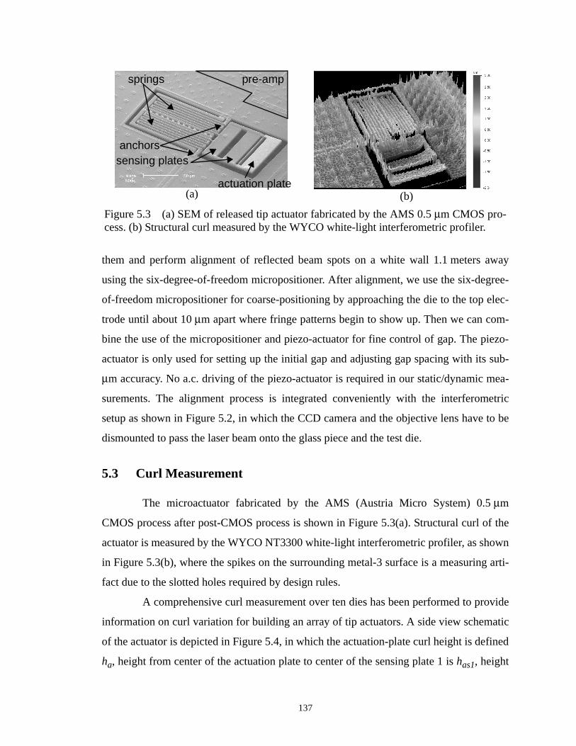
them and perform alignment of reflected beam spots on a white wall 1.1 meters away
using the six-degree-of-freedom micropositioner. After alignment, we use the six-degree-
of-freedom micropositioner for coarse-positioning by approaching the die to the top elec-
trode until about 10 µm apart where fringe patterns begin to show up. Then we can com-
bine the use of the micropositioner and piezo-actuator for fine control of gap. The piezo-
actuator is only used for setting up the initial gap and adjusting gap spacing with its sub-
µm accuracy. No a.c. driving of the piezo-actuator is required in our static/dynamic mea-
surements. The alignment process is integrated conveniently with the interferometric
setup as shown in Figure 5.2, in which the CCD camera and the objective lens have to be
dismounted to pass the laser beam onto the glass piece and the test die.
5.3 Curl Measurement
The microactuator fabricated by the AMS (Austria Micro System) 0.5 µm
CMOS process after post-CMOS process is shown in Figure 5.3(a). Structural curl of the
actuator is measured by the WYCO NT3300 white-light interferometric profiler, as shown
in Figure 5.3(b), where the spikes on the surrounding metal-3 surface is a measuring arti-
fact due to the slotted holes required by design rules.
A comprehensive curl measurement over ten dies has been performed to provide
information on curl variation for building an array of tip actuators. A side view schematic
of the actuator is depicted in Figure 5.4, in which the actuation-plate curl height is defined
ha, height from center of the actuation plate to center of the sensing plate 1 is has1, height
Figure 5.3 (a) SEM of released tip actuator fabricated by the AMS 0.5 µm CMOS pro-cess. (b) Structural curl measured by the WYCO white-light interferometric profiler.
(a) (b)
springs
anchors
pre-amp
actuation plate
sensing plates
137

from center of the actuation plate to center of the sensing plate 2 is has2, the actuation-
plate tilting angle is θa, the sensing-plate-1 tilting angle is θs1, and the sensing-plate-2 tilt-
ing angle is θs2. The angles are defined from the curl heights of plates at edges with
respect to plate centers. Measured results are tabulated in Table 5.1, in which a maximum
difference of 0.9 µm in ha is illustrated. Large θs1, θs2, has1, has2 can reduce damping coef-
ficient compared to a perfect parallel-plate actuator, resulting in phase-margin reduction.
The AMS process does not perform Chemical Mechanical Polishing (CMP) after thin-film
deposition, which can be a factor affecting the curl variation.
Dieha
(µm)has1
(µm)has2
(µm)θa
(deg.)θs1
(deg.)θs2
(deg.)
1 0.9 0.8 0.7 2.58 1.43 -2.86
2 1.3 1.1 1.1 2.29 1.43 -2.58
3 1.2 1.0 1.0 2.86 1.43 -2.86
4 1.2 0.9 0.9 2.58 1.72 -2.86
5 0 0.7 0.5 2.15 1.43 -2.86
6 0.8 1.0 0.6 2.29 1.43 -2.86
7 1.3 1.0 1.0 2.29 1.72 -2.86
8 1.6 1.1 1.3 2.86 2.00 -2.86
9 1.8 1.1 1.0 2.86 1.72 -3.43
10 1.8 1.2 1.0 3.72 1.72 -3.58
Average (µm, deg)
1.19 0.99 0.91 2.65 1.60 -2.96
Std. Dev.(µm, deg.)
0.54 0.15 0.24 0.46 0.20 0.30
Table 5.1: Measured curl and plate tilt of the tip actuator.
Figure 5.4 Side view schematic of the actuator.
θs2
θs1θa
has1has2
spring
sensing plate 2 sensing plate 1 actuation plate
ha
anchor
138
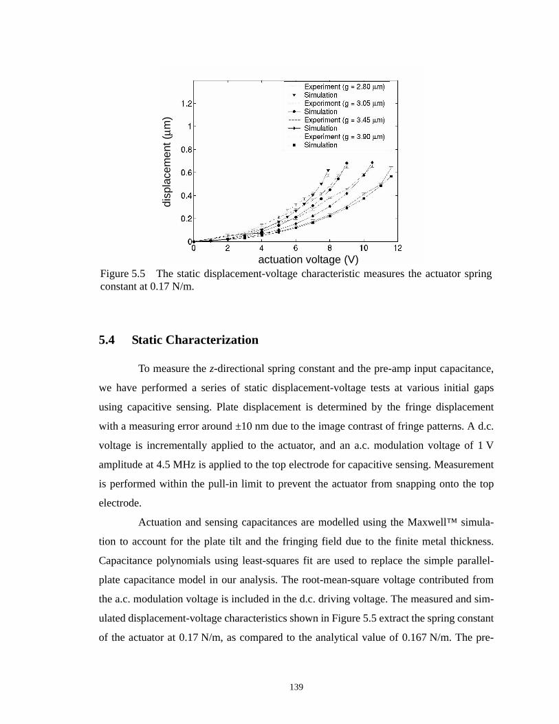
5.4 Static Characterization
To measure the z-directional spring constant and the pre-amp input capacitance,
we have performed a series of static displacement-voltage tests at various initial gaps
using capacitive sensing. Plate displacement is determined by the fringe displacement
with a measuring error around ±10 nm due to the image contrast of fringe patterns. A d.c.
voltage is incrementally applied to the actuator, and an a.c. modulation voltage of 1 V
amplitude at 4.5 MHz is applied to the top electrode for capacitive sensing. Measurement
is performed within the pull-in limit to prevent the actuator from snapping onto the top
electrode.
Actuation and sensing capacitances are modelled using the Maxwell™ simula-
tion to account for the plate tilt and the fringing field due to the finite metal thickness.
Capacitance polynomials using least-squares fit are used to replace the simple parallel-
plate capacitance model in our analysis. The root-mean-square voltage contributed from
the a.c. modulation voltage is included in the d.c. driving voltage. The measured and sim-
ulated displacement-voltage characteristics shown in Figure 5.5 extract the spring constant
of the actuator at 0.17 N/m, as compared to the analytical value of 0.167 N/m. The pre-
Figure 5.5 The static displacement-voltage characteristic measures the actuator springconstant at 0.17 N/m.
actuation voltage (V)
disp
lace
men
t (µm
)
139

amp input capacitance, Ci, is 333 fF extracted from the measured pre-amp output ampli-
tude with respect to the actuator displacement in Figure 5.6. Measured value is smaller
than the extracted capacitance, 408 fF, from layout.
5.5 Capacitive Feedthrough
The capacitance feedthrough from the electrostatic actuator and the capacitive
position sensor gives rise to incorrect sensor outputs after demodulation. As depicted in
Figure 5.7, the baseband actuation voltage, Va, is coupled to the pre-amp output via a
feedthrough capacitance, Cf, which consists of the fringing capacitance, Cf1, between the
crossed actuation and sensing interconnects (a ground shield is inserted in between), and
another fringing capacitance, Cf2, between the top metal layers of the actuation and sens-
ing plates. The total of Cf is 1.38 fF, with Cf1 = 0.42 fF and Cf2 = 0.96 fF obtained by
Maxwell simulation. After the pre-amp, the baseband feedthrough subsequently feeds
through the demodulator with a gain, Adf, to produce a sensed output error, Vf,
Figure 5.6 Characteristic of pre-amp output versus plate displacement results in anextracted pre-amp input capacitance of 333 fF.
pre-
amp
outp
ut a
mpl
itude
(V
)
displacement (µm)
140

(5.1)
We measure the feedthrough transfer function, , using the Agilent 4395A
spectrum/network analyzer by applying a sinusoidal voltage to the actuation plate without
a top electrode. The measured feedthrough gain is -35.9 dB, with -26.4 dB measured after
the pre-amp, and -9.5 dB from the pre-amp to the demodulator. Substituting measured val-
ues and Ci = 333 fF into (5.1) gives Cf = 1.6 fF. For a 10 V actuation voltage, it produces a
significant feedthrough output of 160 mV, which is equivalent to a sensed voltage pro-
duced by a 0.7-µm plate displacement at a 3-µm initial gap.
To suppress the capacitive feedthrough, we perform successive high-pass filter-
ing in the pre-amp and right after the pre-amp, as shown in Figure 5.7, to reduce the
feedthrough gain to -81 dB. The resistors and capacitors used for high-pass filtering are:
C1 = 1 nF, C2 = 390 pF, R1 = 1.52 kΩ, R2 = 13.65 kΩ, and R3 = 3 kΩ.
5.6 Open-Loop Frequency Response
The actuator frequency response of the actuator in Figure 5.8 is measured elec-
tronically by the network analyzer, which supplies an a.c. voltage amplitude of 700 mV
Vf
Cf
Cf Ci+-----------------AvAdf Va=
+
_
R2
R1
Figure 5.7 Schematic of capacitive sensing circuit, illustrating a sensed voltage errorintroduced by capacitive feedthrough from actuation voltage, and reduction offeedthrough by high-pass filtering.
Va
C1
CiCf
•
•• •
R3
C2 ×Vf
+
_
Vc (carrier)
Adf
off-chipoff-chip
Vf s( ) Va s( )⁄
141

with incrementally increased d.c. bias from 0 to 4 V to the actuator, and gathers readout
signal after demodulation. At a frequency around 30 kHz, the measured gain magnitude
starts to increase because of the capacitive feedthrough. Measured resonant frequency
decreases with respect to the increasing d.c. bias due to the spring-softening effect. The
root-mean-square voltage contributed from the a.c. modulation voltage of 1 V amplitude
is included in the d.c. driving voltage for analysis. Measured resonant-frequency shift and
NODAS simulation results are compared in Figure 5.9 for initial gaps of 2.3 µm and
2.65 µm, in which more frequency drop is observed for the smaller initial gap at the same
d.c. actuation voltage. The original actuator resonant frequency, ωn, is found at 12.4 kHz
from the plot.
The effective damping ratio, ξe, given in (4.48), is obtained by comparing the res-
onant peak magnitude of the measured frequency response in Figure 5.10(a) with that of a
second-order system transfer function. ξe is between 0.55 to 0.35 for gaps between 2.3 to
2.65 µm as shown in Figure 5.10(b). Also shown in Figure 5.10(a) and (b) are results from
the NODAS simulation, in which the squeeze-film damping model and the electrostatic
gap model are used for frequency-response simulation. We have considered structural curl
Figure 5.8 Measured frequency response of the actuator driven at different d.c. bias,illustrating the resonant frequency shift due to the spring-softening effect.
gain
(dB
)
frequency (Hz)
phas
e (d
egre
e)
VDC = 1 VVDC = 2 VVDC = 3 VVDC = 4 V
VDC = 1 to 4 V
142

by using different gaps for the actuation and sensing plates, and a ±5% gap variation is
used to account for the plate tilt.
5.7 Open-Loop Step Response
We apply a 2 kHz square-wave voltage with amplitudes ranging from 1 V to
4.8 V (minimum = 0 V) to the actuator with an initial gap spacing of 2.45 µm. The sensed
signal is gathered after demodulation and amplification by a gain of ten, and displayed on
an Agilent 54624A digital oscilloscope averaged over 128 sweeps to remove most of the
1× and 2× carrier-frequency signals. Measured demodulator output voltage waveforms are
shown in Figure 5.11 from which risetime (0 to 100%) and falltime (100 to 0%) are mea-
sured and tabulated in Table 5.2. The risetime increases with the closing of gap due to the
increasing damping coefficient, and spring-softening-induced bandwidth reduction. The
actuator is more lightly damped when moving back to the initial position as evidenced by
the measured larger overshoot, shorter falltime, and longer settling time in Figure 5.11.
Vact (V) Risetime(µs) Falltime(µs)
1.0 29.0 28.02.0 29.2 28.52.8 30.0 28.73.6 30.6 28.84.2 32.0 28.84.8 33.3 28.8
Table 5.2: Open-loop risetime and fall measurements (gap = 2.45 µm).
Figure 5.9 Measured resonant frequency versus d.c. actuation voltage.d.c. bias (V)
reso
nant
freq
uenc
y (k
Hz)
Gap (@ V = 0) = 2.65 µm
Gap (@ V = 0) = 2.3 µm
143
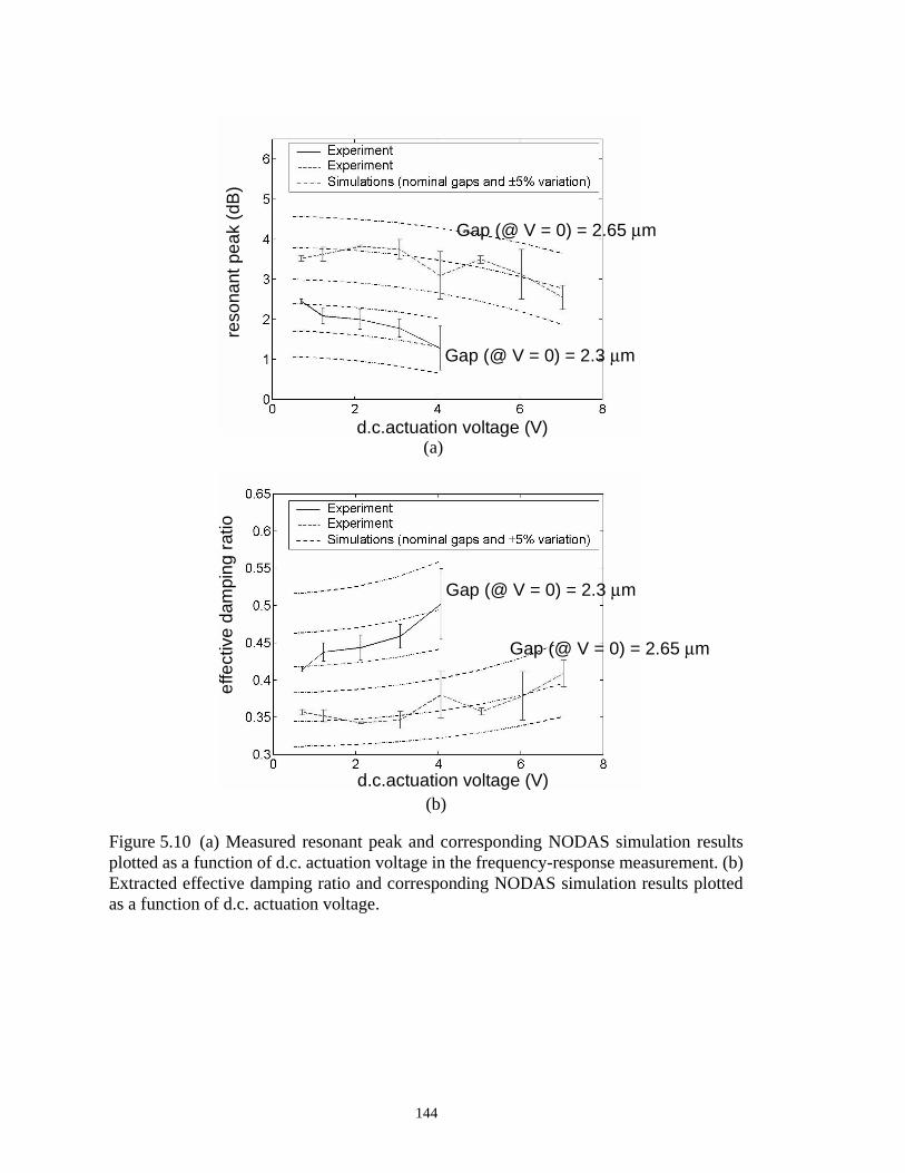
Figure 5.10 (a) Measured resonant peak and corresponding NODAS simulation resultsplotted as a function of d.c. actuation voltage in the frequency-response measurement. (b)Extracted effective damping ratio and corresponding NODAS simulation results plottedas a function of d.c. actuation voltage.
reso
nant
pea
k (d
B)
d.c.actuation voltage (V)
d.c.actuation voltage (V)
effe
ctiv
e da
mpi
ng r
atio
(a)
(b)
Gap (@ V = 0) = 2.65 µm
Gap (@ V = 0) = 2.3 µm
Gap (@ V = 0) = 2.3 µm
Gap (@ V = 0) = 2.65 µm
144

Another measurement of step-response waveforms performed at an initial gap of
3.2 µm with actuation voltage ranging from 1 V to 7 V is shown in Figure 5.12, and the
measured risetime and falltime are tabulated in Table 5.3. From Table 5.2 and Table 5.3,
we observe that the risetime does display an increasing trend with respect to the actuation
Figure 5.11 Open-loop responses to 2 kHz square-wave actuation force varying inapplied voltage amplitude from 1 V to 4.8 V (gap = 2.45 µm).
time (ms)
dem
odul
ator
out
put v
olta
ge (
mV
)
Vact = 4.8 V
4.2 V3.6 V
2.8 V
2.0 V1.0 V
Time (ms)
Dem
odul
ator
out
put v
olta
ge (
mV
)
Figure 5.12 Open-loop responses to 2 kHz square-wave actuation force varying inapplied voltage amplitude from 1 V to 7 V (gap = 3.2 µm).
Vact = 7 V
6 V
5 V
4 V
3 V2 V1 V
145
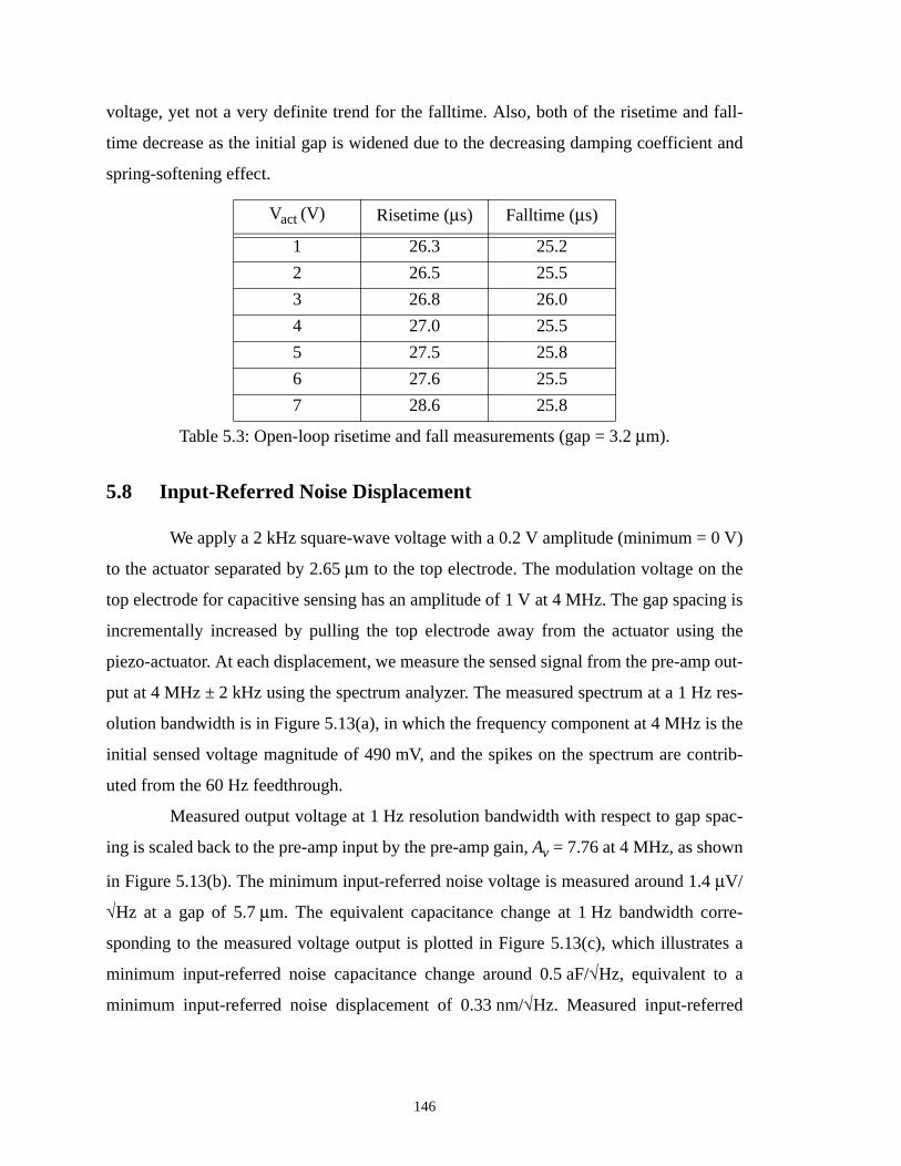
voltage, yet not a very definite trend for the falltime. Also, both of the risetime and fall-
time decrease as the initial gap is widened due to the decreasing damping coefficient and
spring-softening effect.
5.8 Input-Referred Noise Displacement
We apply a 2 kHz square-wave voltage with a 0.2 V amplitude (minimum = 0 V)
to the actuator separated by 2.65 µm to the top electrode. The modulation voltage on the
top electrode for capacitive sensing has an amplitude of 1 V at 4 MHz. The gap spacing is
incrementally increased by pulling the top electrode away from the actuator using the
piezo-actuator. At each displacement, we measure the sensed signal from the pre-amp out-
put at 4 MHz ± 2 kHz using the spectrum analyzer. The measured spectrum at a 1 Hz res-
olution bandwidth is in Figure 5.13(a), in which the frequency component at 4 MHz is the
initial sensed voltage magnitude of 490 mV, and the spikes on the spectrum are contrib-
uted from the 60 Hz feedthrough.
Measured output voltage at 1 Hz resolution bandwidth with respect to gap spac-
ing is scaled back to the pre-amp input by the pre-amp gain, Av = 7.76 at 4 MHz, as shown
in Figure 5.13(b). The minimum input-referred noise voltage is measured around 1.4 µV/
√Hz at a gap of 5.7 µm. The equivalent capacitance change at 1 Hz bandwidth corre-
sponding to the measured voltage output is plotted in Figure 5.13(c), which illustrates a
minimum input-referred noise capacitance change around 0.5 aF/√Hz, equivalent to a
minimum input-referred noise displacement of 0.33 nm/√Hz. Measured input-referred
Vact (V) Risetime (µs) Falltime (µs)
1 26.3 25.2
2 26.5 25.5
3 26.8 26.0
4 27.0 25.5
5 27.5 25.8
6 27.6 25.5
7 28.6 25.8
Table 5.3: Open-loop risetime and fall measurements (gap = 3.2 µm).
146

Figure 5.13 (a) Pre-amp output spectrum measurement to a 2 kHz square-wave actuationvoltage with an amplitude of 0.2 V. (b) Measured input-referred sensed voltage as a func-tion of actuation gap. (c) Equivalent input-referred capacitance change as a function ofactuation gap.
initial sensed voltage @ 4 MHz
sensed voltage @ 4 MHz ± 2 kHz
dBV
kHz
gap (µm)(c)
Mea
sure
d in
put-
refe
rred
cap
acita
nce
gap (µm)(b)
Mea
sure
d in
put-
refe
rred
sen
sed
(a)
volta
ge @
1H
z B
W (
µV)
chan
ge @
1H
z B
W (
aF)
147

noise capacitance change and input-referred noise displacement at g = 5.7 µm are prima-
rily contributed from the thermal noise of d.c.-bias resistor in front of the pre-amp, as
depicted in Figure 3.33(a) and (b).
5.9 Closed-Loop Step Response
The photograph in Figure 5.14 illustrates the PCB with the tip-actuator package
and the off-chip feedback control circuit. The final controller design is C(s) = 24.3, and
the pre-filter design is F(s) = 1/(s/1800 + 1). The controller gain is higher than the previ-
ously designed kp = 16 primarily because of the pre-amp gain Av = 7.76 at the modulation
frequency 4.5 MHz, instead of Av = 10. We apply a 100 Hz square-wave voltage as the
input command for the closed-loop response measurement. Before the command is
applied, an initial d.c. sensed voltage output (103 mV at g = 3.3 µm) is nulled to zero, and
the amplitude of the 1× and 2× carrier-frequency signals (fc = 4.5 MHz) at the controller
output is reduced to within 1 V by low-pass filtering (ωp = 140 kHz).
Measured controller output waveforms and demodulated pre-amp output wave-
forms as the actuated plate moves across and beyond the pull-in instability are averaged
over 128 sweeps on the oscilloscope, as shown in Figure 5.15(a) and Figure 5.15(b). The
relation of plate displacement versus input command voltage amplitude is depicted in Fig-
ure 5.15(c). The decrease of controller output after the pull-in voltage (Vpi = 10.43 V)
pre-filter
controller
demodulator
subtracter
tip actuatorpackage
Figure 5.14 Optical photograph of the PCB with the tip actuator package and off-chipfeedback control circuit.
148

Figure 5.15 (a) Measured controller output waveforms when displaced plate enters pull-in region and beyond. The inset illustrates its waveform when the input command turnsfrom high to low. (b) Measured demodulated pre-amp output waveforms. (c) Plate dis-placement versus input command voltage. (gap = 3.3 µm)
time (ms)
cont
rolle
r ou
tput
(V
)
(a)
time (ms)dem
odul
ated
pre
-am
p ou
tput
(m
V)
(b)
Input command (V)
disp
lace
men
t (µm
)
(c)
149
reduces the stored charge on the plate in order to stabilize the actuator in the open-loop
unstable regime. As the input command changes from high to low, the controller output
first decreases, and then increases as the actuator retracts back to the rest position to main-
tain stability, as shown by the inset in Figure 5.15(a). The peak magnitude shown in the
inset increases as the damping coefficient decreases. The rise time of the plate displace-
ment increases with increased input command magnitude from 2 ms to 5 ms as illustrated
by the demodulated pre-amp output waveforms in Figure 5.15(b). Therefore we have to
decrease the input-command frequency from 100 Hz to 50 Hz for large input commands.
Measured controller output waveforms and demodulated pre-amp output wave-
forms are compared with closed-loop NODAS simulations, in which we model the paral-
lel-plate actuator using 3D elastic beam elements, 3D elastic plate elements, squeeze-film
damping elements, and electrostatic gap models as shown in the schematic in Figure 5.16.
The actual gap values used in the squeeze-film damping models are increased by 1.2 µm
to account for the reduced damping due to plate tilt. The measured and simulated pre-filter
output, controller output, demodulated pre-amp output, and plate displacement to a 50 Hz
square-wave input command are plotted in Figure 5.17 with very good agreement. A max-
imum displacement of 2 µm, equivalent to 60% of the gap (g = 3.3 µm) is illustrated.
Measured falltime of the demodulated pre-amp output waveform is significantly shorter
than its risetime because the actuator dynamics is different in the falling period, in which
the spring restoring force, not the electrostatic force, provides acceleration for the actuator
when it retracts back to the rest position. Also the experienced damping force reduces as
the actuator moves away from the top electrode.
5.10 Discussion
Maximum travel range of 60% of the gap is experimentally demonstrated by
closed-loop servo. Critical factors which contribute to the failure of the closed-loop servo
beyond 60% of the gap are:
(1) Reduced phase margins resulted from an reduced damping coefficient due to plate tilt.
The measured controller output waveform during the input-command transition is
related the damping coefficient at that instant. We match the waveform in NODAS
150
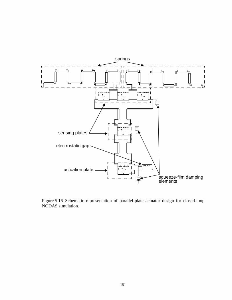
Figure 5.16 Schematic representation of parallel-plate actuator design for closed-loopNODAS simulation.
squeeze-film dampingelements
sensing plates
actuation plate
springs
electrostatic gap
151

Figure 5.17 Measured waveforms (dashed lines) and simulated waveforms (solid lines)of pre-filter output, controller output, demodulated pre-amp output, and plate displace-ment to a 50 Hz square-wave input-command voltage.
time (ms)
disp
lace
men
tpr
e-am
p ou
tput
pre-
filte
r ou
tput
cont
rolle
r ou
tput
(m
V)
(µm
)(V
)(V
)
152

simulation by increasing the gap spacing of squeeze-film damping elements to accom-
modate for the plate tilt. The damping ratio as a function of normalized displacement
is plotted in Figure 5.18(a) for both tilted and parallel plates. The resulting phase mar-
gin versus normalized displacement is shown in Figure 5.18(b), which illustrates a sig-
nificant phase margin loss due to plate tilt as compared to the parallel-plate case. The
phase margin at 60% of the gap is only 11°.
(2) Sensor noise amplification at the controller output. As noted in Section 4.2.1, a large
loop gain at frequencies for which the plant gain is small results in large noise amplifi-
cation at the controller output, and probable system instability. The situation of noise
amplification is worsened when the d.c gain of the actuator reduces as the plate dis-
placement increases as shown in Figure 4.8, leading to noise amplification at low fre-
quencies. We substitute the linearized plant at 60% of the gap (2-µm displacement)
and the controller into (4.13), and plot the noise gain from the capacitive sensor output
to the controller output in Figure 5.19. The plot includes noise gains for displacements
of 1.8 µm and 1.6 µm, demonstrating that as the placement increases, both the noise
gain at low frequencies and its peak value increase. A noise spectral density of 70 µV/
√Hz from the capacitive sensor output is amplified by 44 to 51 dB for frequencies up
to 100 kHz at the controller output. Therefore system stability can by seriously
affected.
(3) Changing sensor output due to thermally-induced plate displacement, charging effect,
and piezo-actuator drift. The actuator is constantly illuminated by a LED, which pro-
duces a 4 °F difference measured between the actuator and the ambient temperatures.
We have observed up to 300 nm plate displacement due to the heating effect. Charging
may occur at the high-impedance sensing node of the pre-amp due to the charge in the
surrounding dielectric layer and air. Due to the fact that there is no feedback loop
around the piezo-actuator, drift up to 100 nm can happen to affect the preset gap spac-
ing. All those effects result in a d.c. offset at the capacitive sensor output, leading to a
d.c. offset about 1 to 2 V at the controller output during the experiment. This offset can
not be nulled immediately when it happens, therefore system stability may be affected.
153
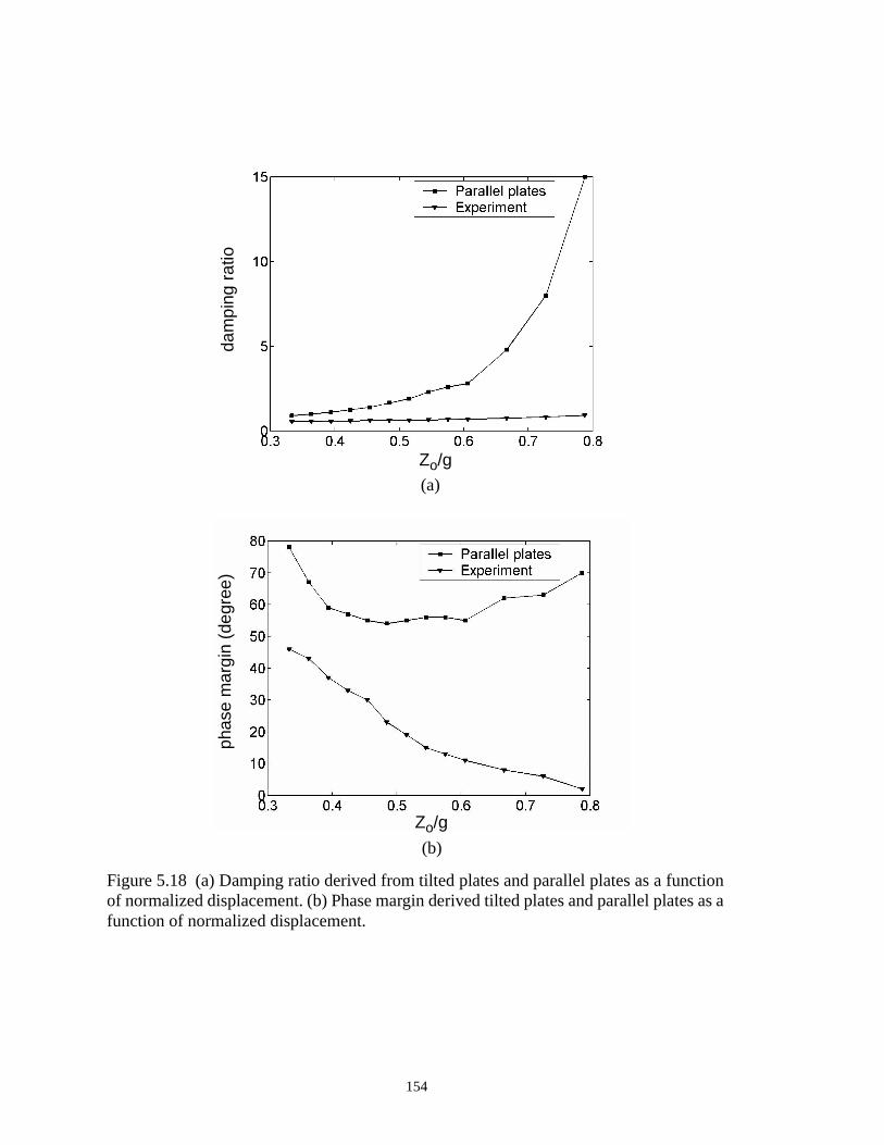
Figure 5.18 (a) Damping ratio derived from tilted plates and parallel plates as a functionof normalized displacement. (b) Phase margin derived tilted plates and parallel plates as afunction of normalized displacement.
dam
ping
rat
io
Zo/g(a)
Zo/g
phas
e m
argi
n (d
egre
e)
(b)
154

Figure 5.19 Noise gain from sensor output to controller output plotted for linearizedplants at different displacements.
Hz
nois
e ga
in (
dB) Zo = 2 µm
Zo = 1.8 µm
Zo = 1.6 µm
155

156

Chapter 6
Conclusions
In this thesis, we have presented a controller design procedure which effectively
resolves the nonlinear and unstable characteristics of the parallel-plate actuator, and leads
to a linear controller design suitable for implementation. We are the first to report success-
ful experimental results of closed-loop voltage control that extend the parallel-plate dis-
placement to 60% of the initial gap, almost doubling the maximum displacement limited
by the pull-in instability. For the proposed probe-based micro disk drives, we prefer to
achieve a displacement up to 75 to 83% of the initial gap (g = 2 to 3 µm) to accommodate
a tip height of 500 nm. Given the achieved 60% travel range, an increase of tip height to
1.2 µm is suggested by stacking up the thin films underneath the tip.
The CMOS-MEMS process developed at Carnegie Mellon is the best to date
enabling technology for implementation of the proposed micro disk drive. Fabrication of
the tip actuator array can benefit from the convenient circuit integration to get high-speed
electronics, and the use of existing multiple interconnects within mechanical structures for
signal routing. To provide material properties for mechanical design, we have character-
ized Young’s modulus, stress gradient, and residual stress of various CMOS-MEMS
structures fabricated from different Agilent 0.5 µm CMOS runs. The commonly used m3-
m2-m1 beam has an average Young’s modulus of 62 GPa, an average radius curvature of
1.37 mm, and an average residual stress of 42.8 MPa.
Controller design is through linearization of the nonlinear plant. Local stability of
the system is analyzed using gain margin and phase margin. To extend from local stability
to global stability in a nonlinear control problem, we perform input-disturbance rejection
to reduce the effects from initial conditions and high-order electrostatic force terms
neglected during plant linearization. There is a design trade-off at large displacements
where a large controller gain is desired for disturbance rejection, yet the large gain
decreases the phase margin at small and median displacements, and induces more noise
amplification at the controller output. Both of them can lead to system instability.
157

We have shown that selection of the two degree-of-freedom control system con-
figuration (controller and pre-filter) is crucial as it decouples the design processes for
closed-loop stability and output tracking. The controller ensures system stability in the
presence of the unstable pole, and the pre-filter shapes the input command for the feed-
back loop to follow. The selected pre-filter design is based on a desired output risetime of
2 to 4 ms. Without the pre-filter, the resultant output may exhibit a large overshoot accord-
ing to our design experience.
As mentioned in Chapter 4, to maintain a 60° phase margin at an unstable operat-
ing point, the minimum open-loop bandwidth should be at least twice of the unstable pole
frequency. Frequency of the unstable pole increases with increasing plate displacement
and decreasing damping ratio. If the system were to be operated at a low pressure for
application of thermally-assisted writing using tunneling current, the reduced damping
ratio will require a large open-loop bandwidth for system stabilization, subsequently
resulting in excessive noise amplification at the controller output, and/or excitation of
higher mechanical modes to destabilize the system. Furthermore, the implemented open-
loop bandwidth is limited by the use of low-pass filtering after the demodulator, thereby
the achieved phase margin is restricted at large displacements and low operating pres-
sures, and design of a stable controller is even more difficult.
Steady-state error resulting from the use of a proportional-gain controller can be
eliminated by adding an integral controller. However, the 90° phase lag introduced by an
integrator has to be compensated by adding a zero at a very low frequency (tens of Hertz);
otherwise the resultant phase margin can be significantly reduced. Special circuit design
techniques are required to realize the low-frequency zero on chip with die area taken into
consideration. The implementation of an integrator requires a reset scheme for cancelling
the integral of circuit non-idealities, such as input offset voltage.
Experimental closed-loop responses have very good agreement with the NODAS
simulations in which 3D plates, 3D beams, squeeze-film damping elements, and electro-
static gap models are used to represent the actuator. Reduced phase margin and increase in
loop noise bandwidth are the key factors which are believed to contribute to the failure of
the closed-loop servo beyond 60% of the gap. The d.c. offset voltage introduced by charg-
ing effect, thermally-induced plate displacement, and piezo-actuator drift can also affect
158

stability if it is not completely nulled during the experiment. The possibility that instability
at atmospheric pressure is caused by excitation of the high-order mechanical modes is
ruled out based on simulation results from NODAS.
6.1 Future Work
This thesis provides a general design procedure for parallel-plate servo using a
linear time-invariant controller, which is less versatile than a nonlinear controller or a lin-
ear time-varying controller in terms of bandwidth efficiency and attainable gain and phase
margins. These types of controller design are promising to further extend the travel range
to the entire gap. The control problem can be of interest to the control system community
as well. One of the possible options for design of a nonlinear controller can use a nonlinear
circuit network to first cancel the plant nonlinearity, followed by conventional design of a
linear controller.
Control of the actuator as it returns back to the rest position is another research
topic equally important to the problem of extending its travel range. We have shown in
Chapter 5 that the closed-loop step response exhibits different risetime and falltime due to
the dissimilar actuator dynamics in the rising and falling periods. Therefore system stabil-
ity is not automatically guaranteed in the falling period by the current controller design.
We have found that a large damping coefficient at small gaps can destabilize the system
during the input-command transition, contrary to its stabilizing effect in the rising period.
The stability issue with respect to the squeeze-film damping coefficient in the returning
pull-out path has to be further analyzed to complete the position-servo cycle. The results
can be utilized in design of the actuator to obtain desired value of damping coefficient.
There is much work to do regarding the fabrication and testing of the tip-actuator
array. Size of the on-chip sensing and control electronics has to be minimized to fit into a
tip-actuator cell, and the circuit power consumption has to be reduced to increase the total
number of active tip actuators for data read and write. The trade-off is that the circuit gain-
bandwidth and noise performance will be negatively impacted by decreased transistor
size. It is reasonable to say that each of the circuit blocks, including controller, pre-amp,
demodulator, subtracter, and pre-filter, can be implemented with a size of at least 30 to
159

50 µm on the side. Therefore, fitting them and the tip actuator all into an 10,000 µm2 tip
actuator cell will be a challenge. The media stroke may have to increase from the current
±50 µm by 50% more to increase the tip actuator cell size by 125%. An even larger
increase of the actuator cell size may be necessary if operational amplifiers are used to
implement pre-amp, controller, and pre-filter for precise gains, which are highly desirable
to better ensure stability robustness. In addition, the passive components used for filtering
out capacitive feedthrough can also take up large areas. A better demodulation circuit with
less feedthrough needs to be built to prevent undesired signals from being modulated into
the signal band. High-voltage MOSFET transistors providing up to ±15 V need to be fab-
ricated. This voltage value becomes larger if the desired closed-loop response has to be
much faster than milli-seconds. From the supplied-voltage standpoint, it is not necessary
to use a state-of-the-art sub-micron CMOS process for fabrication of the tip-actuator
array. The amount of current in the control circuit is not limited by slew rate since the
actuated capacitance is only 10 to 20 fF, and the controller output changes in milli-sec-
onds. Required current is more related to providing large transconductances for building
high-speed electronics (gain-bandwidth product > 20 MHz). Finally, stability robustness
against external shock forces should also be analyzed and experimentally tested as the
commercial portable disk drives. Currently there is not a pull-down electrode in the actua-
tor design to actively prevent the snap-in. This part of the research can be further explored
in the future.
160

Bibliography
[1] M. Madou, Fundamentals of Microfabrication, pp. 406-410, CRC press, Boca
Raton, Florida, 1997.
[2] Y. Nemirovsky and O. Bochobza-Degani, “A methodology and model for the pull-in
parameters of electrostatic actuators,” J. of Microelectromechanical Systems, vol. 10,
no. 4, pp. 601-615, 2001.
[3] P. M. Osterberg and S. D. Senturia, “M-TEST: a test chip for MEMS material prop-
erty measurements using electrostatically actuated test structures,” J. of Microelec-
tromechanical Systems, vol. 6, pp. 107-118, June 1997.
[4] G. B. Hocker, D. Youngner, E. Deutsch, A. Volpicelli, S. Senturia, M. Butler, M.
Sinclair, T. Plowman, and A. J. Ricco, “The polychromator: a programmable MEMS
diffraction grating for synthetic spectra,” Technical Digest. Solid-State Sensor and
Actuator Workshop, Hilton Head Island, SC, USA, pp. 89-92, 2000.
[5] C. Marxer, C. Thio, M. A. Gretillat, N. F. de Rooij, R. Battig, O. Anthamatten, B.
Valk, and P. Vogel, “Vertical mirrors fabricated by deep reactive ion etching for
fiber-optic switching applications,” J. of Microelectromechanical Systems, vol. 6, pp.
277-285, Sept. 1997.
[6] J. Buhler, J. Funk, J. G. Korvink, F. P. Steiner, P. M. Sarro, and H. Baltes, “Electro-
static aluminum micromirrors using double-pass metallization,” J. of Microelectro-
mechanical Systems, vol. 6, pp. 126-135, June 1997.
[7] L. J. Hornbeck, “Deformable-mirror spatial light modulators,” SPIE Critical Review
Series, vol. 1150, pp. 86-102, 1989.
161

[8] P. M. Zavracky, S. Majumber, and E. McGruer, “Micromechanical switches fabri-
cated using nickel surface micromachining,” J. of Microelectromechanical Systems,
vol. 6, pp. 3-9, Mar. 1997.
[9] K. Sato and M. Shikida, “Electrostatic film actuator with a large vertical displace-
ment,” Micro Electro Mechanical Systems’92, Travemunde, Germany, pp. 1-5,
1992.
[10] R. Jebens, W. Trimmer, and J. Walker, “Microactuators for aligning optical fibers,”
Sensors and Actuators A (Physical), vol. 2, pp. 65-73, 1989.
[11] E. S. Hung, “Positioning, control, and dynamics of electrostatic actuators for use in
optical systems,” Ph.D. dissertation, Dept. of Electrical Engineering and Computer
Science, Massachusetts Institute of Technology, Cambridge, Massachusetts, 1998.
[12] X. T. Wu, R. A. Brown, S. Mathews, and K. R. Farmer, “Extending the travel range
of electrostatic micro-mirrors using insulator coated electrodes,” in Proc. IEEE/
LEOS int. conf. Opt. MEMS 2000, Kauai, HI, pp. 151-152, 2000.
[13] C. Cabuz, “Dielectric related effects in micromachined electrostatic actuators,” Conf.
on Electrical Insulation and Dielectric Phenomena, pp. 327-332, 1999.
[14] R. Legtenberg, J. Gilbert, S. D. Senturia, and M. Elwenspoek, “Electrostatic curved
electrode actuators,” J. of Microelectromechanical Systems, vol. 6, no. 3, pp. 257-
265, 1997.
[15] E. S. Hung and S. D. Senturia, “Extending the travel range of analog-tuned electro-
static actuators,” J. of Microelectromechanical Systems, vol. 8, no. 4, pp. 497-505,
Dec. 1999.
162
[16] D. M. Burns and V. M. Bright, “Nonlinear flexures for stable deflection of an elec-
trostatically actuated micromirror,” Proceedings of SPIE - the International Society
for Optical Engineering, vol. 3226, pp. 125-136, 1997.
[17] E. K. Chan and R. W. Dutton, “Electrostatic micromechanical actuator with
extended range of travel,” J. of Microelectromechanical Systems, vol. 9, no. 3, pp.
321-328, Sept. 2000.
[18] J. I. Seeger and S. B. Crary, “Stabilization of electrostatically actuated mechanical
devices,” International Conference on Solid-State Sensors and Actuators (Transduc-
ers ‘97), Chicago, IL, USA, pp. 1133-1136, June 16-19, 1997.
[19] L. M. Castañer and S. D. Senturia, “Speed-energy optimization of electrostatic actu-
ators based on pull-in,” J. of Microelectromechanical Systems, vol. 8, no. 3, pp. 290-
298, Sept. 1999.
[20] R. Nadal-Guardia, R. Aigner, W. Nessler, M. Handtmann, and L. M. Castañer, “Con-
trol positioning of torsional electrostatic actuators by current driving,” The Third
International Euroconference on Advanced Semiconductor Devices and Microsys-
tems, Sinolenice Castle, Slovakia, pp. 91-94, 2000.
[21] R. Nadal-Guardia, A. Dehé, R. Aigner, and L. M. Castañer, “Current drive methods
to extend the range of travel of electrostatic microactuators beyond the voltage pull-
in point,” J. of Microelectromechanical Systems, vol. 11, no. 3, pp. 255-263, June
2002.
[22] R. Nadal-Guardia, A. Dehé, R. Aigner, and L. M. Castañer, “New current drive
method to extend the stable operation range of electrostatic actuators: experimental
163

verification,” in Proc. Int. Conf. on Solid State Sensors and Actuators (Transducers
‘01), Munich, pp. 760-763, June 2001.
[23] J. Pons-Nin, A. Rodríguez, and L. M. Castañer, “Voltage and pull-in time in current
drive of electrostatic actuators,” J. of Microelectromechanical Systems, vol. 11, no.
3, pp. 196-205, June 2002.
[24] L. M. Castañer, J. Pons-Nin, R. Nadal-Guardia, and A. Rodríguez, “Analysis of the
extended operation range of electrostatic actuators by current pulse drive,” Sensors
and Actuators A (Physical), vol. 90, pp. 181-190, May 2001.
[25] J. I. Seeger and B. E. Boser, “Dynamics and control of parallel-plate actuators
beyond the electrostatic instability,” in Proc. Transducers’99, Sendai, Japan, pp.
474-477, June 7-10, 1999.
[26] P. B. Chu and K. S. Pister, “Analysis of closed-loop control of parallel-plate electro-
static microgrippers,” in Proc. IEEE int. conf. Robotics and Automation, San Diego,
CA, pp. 820-825, May 8-13, 1994.
[27] D. F. Guillou, “Control of MEMS electrostatic parallel-plate actuators,” Ph.D. dis-
sertation, Dept. of Electrical and Computer Engineering, Carnegie Mellon Univer-
sity, Pittsburgh, Pennsylvania, May, 2002.
[28] L. R. Carley, J. A. Bain, G. K. Fedder, D. W. Greve, D. F. Guillou, M. Lu, T.
Mukherjee, S. Santhanam, L. Abelmann, and S. Min, “Single-chip computers with
microelectromechanical system-based magnetic memory,” Journal of Applied Phys-
ics, vol. 87, no. 9, pt. 1-3, pp. 6680-6685, 2000.
[29] P. Vettiger, G. Cross, M. Despont, U. Drechsler, U. Durig, B. Gotsmann, W. Hab-
erle, M. A. Lantz, H. E. Rothuizen, R. Stutz, G. K. Binnig, “The “millipede”- nano-
164
technology entering data storage,” IEEE Trans. on Nanotechnology, vol. 1, no. 1, pp.
39-55, Mar. 2002.
[30] J. F. Alfaro and G. K. Fedder, “Actuation for probe-based data storage,” Interna-
tional Conference on Modeling and Simulation of Microsystems, Puerto Rico, pp.
202-205, April 21-25, 2002.
[31] M. S.-C. Lu and G. K. Fedder, “Parameterized electrostatic gap models for structured
design of microelectromechanical systems,” International Conference on Modeling
and Simulation of Microsystems, Puerto Rico, pp. 280-283, 1999.
[32] G. K. Fedder and Q. Jing, “A hierarchical circuit-level design methodology for
microelectromechanical systems,” IEEE Trans. on Circuits and Systems II: Analog
and Digital Signal Processing, vol. 46, no. 10, pp. 1309-1315, 1999.
[33] J. Vandemeer, M. S. Kranz, and G. K. Fedder, “Hierarchical representation and sim-
ulation of micromachined inertia sensors,” International Conference on Modeling
and Simulation of Microsystems, Semiconductors, Sensors and Actuators, Santa
Clara, CA, April 6-8, 1998.
[34] N. R. Swart, S. F. Bart, M. H. Zaman, M. Mariappan, J. R. Gilbert, and D. Murphy,
“AutoMM: automatic generation of dynamic macromodels for MEMS devices,” in
Tech. Digest IEEE Micro Electro Mech. Syst. Workshop, Heidelberg, Germany, pp.
178-183, 1998.
[35] D. A. Koester, R. Mahadevan, and K. W. Markus, Multi-User MEMS Processes
(MUMPs) Introduction and Design Rules, available from MCNC MEMS Technol-
ogy Applications Center, 3021 Cornwallis Road, Research Triangle Park, NC 27709,
rev. 3, Oct. 1994, 39 pages.
165

[36] W. A. Johnson and L. K. Warne, “Electrophysics of micromechanical comb actua-
tors,” J. of Microelectromechanical Systems, vol. 4, no. 1, pp. 49-59, 1995.
[37] J. A. Yeh, C. Hui, and C. T. Tien, “Electrostatic model for an asymmetric comb-
drives,” J. of Microelectromechanical Systems, vol. 9, no. 1, pp. 126-136, 2000.
[38] G. S. Samudra and H. L. Lee, “A set of analytic formulas for capacitance of VLSI
interconnects of trapezium shape,” IEEE trans. on Electron Devices, vol. 41, no. 8,
pp. 1467-1469, 1994.
[39] T. C. Edwards, Foundations for microstrip circuit design, John Wiley & Sons, New
York, New York, 1983.
[40] H. H. Woodson and J. R. Melcher, Electromechanical Dynamics, Part I: Discrete
Systems, chapter 3, John Wiley & Sons, New York, 1968.
[41] W. C. Tang, T.-C. H. Nguyen, and R. T. Howe, “Laterally driven polysilicon reso-
nant microstructures,” IEEE Micro Electro Mechanical Systems Workshop, Salt
Lake City, Utah, pp. 53-59, February, 1989.
[42] Maxwell 2D Field Simulator: User’s Reference. Ansoft Corporation, Pittsburgh,
June, 1994.
[43] H. B. Palmer, “The capacitance of a parallel-plate capacitor by the Schwartz-Christ-
offel transformation,” Electrical Engineering 56, pp. 363-366, March, 1937.
[44] I. Getreu, “Behavioral modeling of analog blocks using the SABER simulator,”
Proc. Microwave Circuits and Systems, pp. 977-980, August 1989.
[45] Memcad 4.2 manual, Coventor, Inc., Cambridge, MA, 2001.
[46] R. S. Vanha, F. Kroener, T. Olbrich, R. Baresch, and H. Baltes, “Trench-hall
devices,” J. of Microelectromechanical Systems, vol. 9, no. 1, pp. 82-87, 2000.
166
[47] L. P. Parameswaran, C. H. Hsu, and M. A. Schmidt, “A merged MEMS-CMOS pro-
cess using silicon wafer bonding,” IEDM’95 Technical Digest, pp. 613-616, 1995.
[48] K. H.-L. Chau, S. R. Lewis, Y. Zhao, R. T. Howe, S. F. Bart, and R. G. Marcheselli,
“An integrated force-balanced capacitive accelerometer for low-g applications,” Sen-
sors and Actuators A (Physical), vol. 54, pp. 472-476, 1996.
[49] D. S. Eddy, D. R. Sparks, “Application of MEMS technology in automotive sensors
and actuators,” Proc. IEEE, 86, pp. 1747-1755, 1998.
[50] S. Michaelis, H.-J. Timme, M. Wycisk, and J. Binder, “Acceleration threshold
switches from an additive electroplating MEMS process,” Sensors and Actuators A
(Physical), vol. 85, pp. 418-423, 2000.
[51] B. E. Cole, R. E. Higashi, and R. A. Wood, “Monolithic two-dimensional arrays of
micromachined microstructures for infrared applications,” Proc. IEEE, 86, pp. 1679-
1686, 1998.
[52] G. K. Fedder, S. Santhanam, M. L. Reed, S. C. Eagle, D. F. Guillou, M. Lu, and L. R.
Carley, “Laminated high-aspect-ratio microstructures in a conventional CMOS pro-
cess,” Sensors and Actuators A (Physical), vol. 57, no. 2, pp. 103-110, 1997.
[53] S. Wolf and R. N. Tauber, Silicon Processing for the VLSI Era, 1990.
[54] X. Zhu, D. W. Greve, R. Lawton, N. Presser, and G. K. Fedder, “Factorial experi-
ment on CMOS-MEMS RIE post processing,” in Proc. of the 194th Electrochemical
Society Meeting, Symposium on Microstructures and Microfabricated System, Bos-
ton, MA, pp. 41-44, 1998.
[55] X. Zhu, D. W. Greve, and G. K. Fedder, “Characterization of silicon isotropic etch
by inductively coupled plasma etch in post-CMOS processing,” The Thirteenth
167

Annual International Conference on Micro Electro Mechanical Systems, pp. 568-
573, 2000.
[56] M. S.-C. Lu, X. Zhu, and G. K. Fedder, “Material property measurement of 0.5 µm
CMOS microstructures,” Microelectromechanical structures for Materials Research
Symposium, San Francisco, CA, pp. 27-32, April 15-16, 1998.
[57] S. S. Rao, Mechanical Vibrations, 2nd Edition, Addison-Wesley Publishing Com-
pany, 1990.
[58] Y. B. Gianchandani and K. Najafi, “Bent-beam strain sensors,” J. of Microelectro-
mechanical Systems, vol. 5, no. 1, pp. 52-58, 1996.
[59] H. Lakdawala and G. K. Fedder, “Analysis of temperature-dependent residual stress
gradients in CMOS micromachined structures,” in Proc. Transducers’99, Sendai,
Japan, pp. 526-529, June 7-10, 1999.
[60] S. B. Brown and E. Jansen, “Reliability and long term stability of MEMS,” Digest.
IEEE/LEOS Summer Topical Meetings, Advanced Applications of Lasers in Materi-
als Processing, Broadband Optical Networks - Enabling Technologies and Applica-
tions; Smart Pixels; Optical MEMS and their Applications, pp. 9-10, 1996.
[61] G. K. Fedder, “Simulation of Microelectromechanical Systems,” Ph.D. dissertation,
Dept. of Electrical Engineering and Computer Science, University of California at
Berkeley, Berkeley, California, 1994.
[62] J. S. Przemieniecki, Theory of Matrix Structural Analysis, pp. 70-82, Dover, 1985.
[63] T. Y. Yang, Finite Element Structural Analysis, Prentice-Hall, Inc, 1986.
[64] MATLAB User’s Guide, The MathWorks, Inc., Natick, Massachusetts, 2001.
168
[65] J. J. Blech, “On isothermal squeeze films,” J. Lubrication Tech., vol. 105, pp. 615-
620, 1983.
[66] W. A. Gross, Gas Film Lubrication, Wiley, New York, 1962.
[67] T. Veijola, H. Kuisma, J. Lahdenperä, and T. Ryhänen, “Equivalent-circuit model of
the squeezed gas film in a silicon accelerometer,” Sensors and Actuators A (Physi-
cal), vol. 48, pp. 239-248, 1995.
[68] S. Vemuri, G. K. Fedder, and T. Mukherjee, “Low-order squeeze film model of sim-
ulation of MEMS devices,” International Conference on Modeling and Simulation of
Microsystems, San Diego, CA, pp. 205-209, March 27-29, 2000.
[69] D. A. Johns and K. Martin, Analog Integrated Circuit Design, pp. 259-260, John
Wiley and Sons, Inc., 1997.
[70] J. Singh, Semiconductor Devices, An Introduction, pp. 139-140, McGraw-Hill, Inc.,
1994.
[71] P. R. Gray and R. G. Meyer, Analysis and Design of Analog Integrated Circuits,
Third Edition, John Wiley and Sons, Inc., pp. 667-681, 1994.
[72] J. Wu, “Sensing and control electronics for low-mass low-capacitance MEMS accel-
erometers,” Ph.D. dissertation, Dept. of Electrical and Computer Engineering, Carn-
egie Mellon University, Pittsburgh, Pennsylvania, May, 2002.
[73] T. B. Gabrielson, “Mechanical-thermal noise in micromachined acoustic and vibra-
tion sensors,” IEEE Trans. on Electron Devices, ED-40(5), pp. 903-909, 1993.
[74] M. Vidyasagar, R. K. Bertschmann, and C. S. Sallaberger, “Some simplifications of
the graphical Nyquist criterion,” IEEE Trans. on Automatic Control, vol. 33, no. 3,
pp. 301-303, 1988.
169

[75] N. Cohen, Y. Chait, O. Yaniv, and C. Borghesani, “Stability analysis using Nichols
charts,” Int. J. Robust and Nonlinear Control, vol. 4, pp. 3-20, 1994.
[76] H. W. Bode, Network Analysis and Feedback Amplifier Design, van Nostrand, New
York, 1945.
[77] I. M. Horowitz, Quantitative Feedback Design Theory - QFT. QFT Publications,
Boulder, Colorado, 1992.
[78] J. S. Freudenberg, and D. P. Looze, Frequency domain properties of scalar and mul-
tivariable feedback systems, Lecture Notes in Control and Information Sciences,
edited by M. Thoma and A. Wyner. Springer-Verlag Berlin, Heidelberg, 1988.
[79] D. P. Looze, and J. S. Freudenberg, “Limitations of feedback properties imposed by
open-loop right half plane poles,” IEEE trans. on Automatic Control, vol. 36, no. 6,
pp. 736-739, June, 1991.
[80] J. E. Slotine and W. Li, Applied nonlinear control, Prentice-Hall, Inc., 1991.
[81] I. M. Horowitz and M. Sidi, “Synthesis of feedback systems with large plant igno-
rance for prescribed time-domain tolerances,” Int. J. Control, vol. 16, no. 2, pp. 287-
309, 1972.
[82] Y. Chait and O. Yaniv, “Multi-input/single output computer aided control design
using the Quantitative Feedback Theory,” Int. J. Robust and Nonlinear Control, vol.
3, pp. 47-54, 1993.
[83] I. Horowitz and M. Sidi, “Optimum synthesis of non-minimum phase feedback sys-
tems with plant uncertainty,” Int. J. Control, vol. 27, no. 3, pp. 361-386, 1978.
170

[84] W. Chen and D. J. Ballance, “QFT design for uncertain nonminimum phase and
unstable plants,” Proc. of the American Control Conference, Philadelphia, Pennsyl-
vania, pp. 2486-2490, 1998.
[85] http://www.piezojena.com.
171

172

Appendix A
Electrostatic Gap Model
Electrostatic gap models presented in Chapter 2 are programmed by the Analogy
MAST language for simulation in SABER. The following file (gap_parallel.sin) is the
implemented electrostatic gap model for parallel plates.
#*******************************************************************## MAST Code for an electrostatic gap in the x-direction ## Jan E. Vandemeer and Michael Kranz# Carnegie Mellon University # Michael Lu 8/6/98 # Qi Jing 8/10/98 #*******************************************************************#element template gap_parallel x_a_t x_b_t x_a_b x_b_b \ y_a_t y_a_b y_b_t y_b_b \ phi_a_t phi_a_b phi_b_t phi_b_b \v_a_t v_a_b v_b_t v_b_b = finger_w_t, finger_w_b, finger_length, gap, overlap, topology
translational_pos x_a_t, #x-displacement and force at port "x_a_t" y_a_t, #y-displacement and force at port "y_a_t" x_a_b, #x-displacement and force at port "x_a_b" y_a_b, #y-displacement and force at port "y_a_b" x_b_t, #x-displacement and force at port "x_b_t" y_b_t, #y-displacement and force at port "y_b_t" x_b_b, #x-displacement and force at port "x_b_b" y_b_b, #y-displacement and force at port "y_b_b"
rotational_ang phi_a_t, #Angle displacement about z angle and torque phi_a_b, #Angle displacement about z angle and torque phi_b_t, #Angle displacement about z angle and torque phi_b_b #Angle displacement about z angle and torque
electrical v_a_t, v_a_b, v_b_t, v_b_b #input & output voltage
number finger_w_t = undef #width of the top fingernumber finger_w_b = undef #width of the bottom fingernumber finger_length = undef #width of the top and bottom fingersnumber gap = undef #Gap between the two beamsnumber overlap = undef #X-overlap between the beamsnumber topology = undef #Situation of top beam relative to bottom beam
173

</afs/ece/usr/mslu/.vol1/saber/MSM99/tech_file.sin
number x,th, k1,k2,k3numberntv_ox_t = 20n #Native oxide thickness around the fingers
val frc_N fyd1, fyd2val frc_N fxd1, fxd2val pos_m ovrlp #overlap of beamsval pos_m pt_x, pb_x, mt_x, mb_x val pos_m pt_y, pb_y, mt_y, mb_y val pos_m tmpval pos_m dy #The displacements in ynumber ydc #The DC value of y position.val ang_rad dphival v vltval c cap #capacitance between comb-fingersval v vltg #v^2val nu const, #state, digital on or off-alternates force functionconst2 #the spring constant (after crashing)val nu length # comb-finger lengthval q q1,q2val pos_m g_effval nu w # force per unit lengthval nu slope
#whenever you have the two beams crash, shorten time steps to help simulator
#Parameters sectionparametersydc = gap + finger_w_t/2 + finger_w_b/2if (overlap == undef)error("Overlap is undefined, please give a numerical value.")if (finger_w_b == undef)error("Bottom fingers width is undefined, please give a numerical value.")if (finger_w_t == undef)error("Top fingers width is undefined, please give a numerical value.")if (finger_length == undef)error("Top and bottom finger length is undefined, please give a numerical value.") if (gap == undef)error("Gap is undefined, please give a numerical value.")if (topology < 0 | topology > 1)error("Invalid topology, must be either ’0’ or ’1’, see ’help’ for descriptions.")
174

# coeff. in capacitance and electrostatic-force eqations
x = finger_w_t/poly1_t # ratio of finger width to finger thickness th = 1.496 # sidewall anglek1 = -1.565+0.2818/(x**0.04348) - 2.986*(th**5.900) + 0.4446*exp(th)* (th**6.002) +28.87*ln(th)
k2=21.43-15.50/(x**0.02146) - 10.07*exp(th)/(x**0.03944)/(th**1.877)+ 23.70*(th**0.09913) + 0.04840*exp(x)*(th**0.8278)/(x**2.244)-13.60*ln(th)
k3=10.86- 1.512/(x**0.2517) - 0.007964*(th**15.31)+0.005087*ln(x)-62.71*ln(th)+20.05*(th**2.529)*ln(th)/(x**0.002656)
#values sectionvalues
pt_x = pos_m(x_b_t)pb_x = pos_m(x_b_b)mt_x = pos_m(x_a_t)mb_x = pos_m(x_a_b)pt_y = pos_m(y_b_t)pb_y = pos_m(y_b_b)mt_y = pos_m(y_a_t)mb_y = pos_m(y_a_b)
# topology = 0 means that the top finger is located to the right of the bottom finger, and# topology = 1 means the opposite if (topology == 0) ovrlp = overlap + (pb_x-mt_x) dy = (pos_m(y_b_b,y_b_t)+pos_m(y_a_b,y_a_t))/2 vlt = v(v_b_b,v_a_t) else if (topology == 1) ovrlp = overlap +(pt_x-mb_x) dy = (pos_m(y_b_b,y_b_t)+pos_m(y_a_b,y_a_t))/2 vlt = v(v_a_b,v_b_t)
slope = E*ovrlp*poly1_t/(finger_w_t/2 + finger_w_b/2)
if((gap - dy) > ntv_ox_t)const = 1const2 = 0elseconst = 0const2 = slope
175

vltg = (vlt)**2
g_eff = (1-const)*ntv_ox_t + const*(gap - dy) cap=eps0*poly1_t*ovrlp*(k1+g_eff/PI/poly1_t*(k2+k3* ln(PI* poly1_t/g_eff)))/g_eff if (topology == 1) phi = ang_rad(phi_b_t,phi_a_b) fxd1=-vltg/2*eps0*poly1_t*(k1+g_eff/PI/poly1_t*(k2+k3*ln(PI *poly1_t/g_eff)))/g_eff fxd2 = 0 w=(vltg/2*(k1*eps0*poly1_t*ovrlp/((g_eff)**2)+k3*eps0*ovrlp/PI/g_eff) - const2*(dy-gap+ntv_ox_t))/(ovrlp+1p)
fyd1 = w/2*(ovrlp+(ovrlp**2)/(finger_length+1p)) fyd2 = w/2*(ovrlp-(ovrlp**2)/(finger_length+1p)) q1=abs(v(v_b_t,v_a_b))*cap q2=0
else if (topology == 0) dphi = ang_rad(phi_a_t,phi_b_b) fxd2=vltg/2*eps0*poly1_t*(k1+g_eff/PI/poly1_t*(k2+k3*ln(PI *poly1_t/g_eff)))/g_eff fxd1 = 0 w=(vltg/2*(k1*eps0*poly1_t*ovrlp/((g_eff)**2)+k3*eps0*ovrlp/PI/g_eff) - const2*(dy - gap + ntv_ox_t))/(ovrlp+1p)
fyd2 = w*(ovrlp-(ovrlp**2)/2/(finger_length+1p)) fyd1 = w*(ovrlp**2)/2/(finger_length+1p)
q1=0 q2=abs(v(v_a_t,v_b_b))*cap
equations
i(v_a_b->v_b_t) += d_by_dt(q1)i(v_a_t->v_b_b) += d_by_dt(q2)
frc_N(x_b_t->x_a_b) -= fxd1frc_N(x_a_t->x_b_b) -= fxd2
frc_N(y_b_t->y_a_b) -= fyd1 frc_N(y_a_t->y_b_b) -= fyd2
176

Appendix B
Control System Electronics
OPA27+
_ +15V
-15V
OPA27+
_ +15V
-15VLT7171
+
_ +15V
-15V
dem
odul
atio
nLT1468+
_+15V
-15V
LT1468+
_+15V
-15V
LT1468+
_+15V
-15V
LT1222+
_+15V
-15V
Figure B.1 Schematic of feedback control board. Controller gain kp = 24.3 is split intotwo parts (24.3 = 10 × 2.43). The gain of ten is placed after subtraction of the initialsensed voltage.
Par
alle
l pla
te a
ctua
tor
(LM
149
6)
LT1468+
_ +15V
-15V
actu
atio
n
pre-
amp
outp
ut
Vo-
Vo+
Vcomd
Vinit
pre-filter
2-to-1 conversion andinitial sensed voltagesubtraction
controller
subtracter controller
0.47 µF
1.21κ
1κ
1κ
2k
2k
2k
2k
3.01k
2.1k
2k
2k
2k
2k
1k
909
177

Figure B.2 Schematic of demodulation circuit.
2 3
8
10
1
4
14 5
12
6
150
1k
7507501k1k1k
0.1 µF
0.1 µF
0.1 µF
0.47 µF6.8k
2.47 µF
-8 V
+12 V
100 1000.1 µF
LM1496
Vo+
Vo-
carrier input
signal input
178