pan9420 - eu.industrial.panasonic.com · p a n t e n n a nc wpdn nc w resetn gnd gnd gnd tdo tck...
TRANSCRIPT

PAN9420 Fully Embedded Stand-Alone Wi-Fi Module
Design Guide
Rev. 1.1
Wireless Modules

PAN9420 Wi-Fi Module
Design Guide Rev. 1.1 Page 2
Overview
The PAN9420 is a 2.4 GHz ISM band Wi-Fi
embedded module which includes a wireless radio
and an MCU for easy integration of
Wi-Fi connectivity into various electronic devices.
Features
• Fully embedded: integrated full-featured network stack
• Contains all necessary IoT functionality (Place and Play)
• Integrated web server with AJAX/JSON for web applications
• No stack or software implementation needed on a host MCU
• Simultaneous support of access point- and Infrastructure mode
• Fully automatical IP configuration
• DHCP server offers IP configuration in AP mode
• Access by names (http://yourdevice)
• Integrated TCP/IP network stack: IPv4, ARP, and Auto IP
• Supports TLS/SSL, HTTPS and Wi-Fi security (WPA2-PSK) for secure data connection Over-the-Air firmware update
• Two UART interfaces (command and transparent data)
• Integrated QSPI flash memory for customer web contents and configuration file
• Programming via standard JTAG
• Evaluation kit with pre-installed web application for quick prototyping available
• Evaluation and development tool WiFigurator for Windows
• Getting started tutorials, PC tool, Quick Start Guide
• Wide temperature range of -40 °C to +85 °C
Characteristics
• Surface Mount Type (SMT) 29.0 mm x 13.5 mm x 2.66 mm
• Marvell® 88MW300 MCU/WLAN System-on-Chip
(SoC) inside
• Tx power up to +16 dBm @ IEEE 802.11b
• Rx sensitivity of -97 dBm @ IEEE 802.11b DSSS 1 Mbps
• 20 MHz channels up to 72 Mbps
• Power supply 3.0 V-3.6 V
• Current consumption 150 mA (mix mode
Tx/Rx @ 11b, 11 Mbps), 75 mA Rx, 310 mA Tx
peak
• Power down mode < 1 mA power consumption
• Low power mode available
Block Diagram
Chip
Antenna
SPDT
88MW300
MCU/Radio SoC
Crystal
32.768 kHz
QSPI Flash
32 MbitSPI
UART0
UART1
GPIOs
Status LEDs
MCU Ready
Resetn
Factory Reset
V SPDT
Wake Ups
JTAG
Vcc 3.3 V
LPF
RF-Pad
PAN9420
Fully Embedded Wi-Fi Module
IEEE 802.11 b/g/n
Crystal
38.4 MHz
PAN9420 Wi-Fi Module
Design Guide Rev. 1.1 Page 3
By purchase of any of the products described in this document the customer accepts the document's
validity and declares their agreement and understanding of its contents and recommendations. Panasonic
Industrial Devices Europe GmbH (Panasonic) reserves the right to make changes as required at any time
without notification. Please consult the most recently issued Design Guide before initiating or completing a
design.
© Panasonic Industrial Devices Europe GmbH 2019.
This specification sheet is copyrighted. Reproduction of this document is permissible only if reproduction is
without alteration and is accompanied by all associated warranties, conditions, limitations, and notices. Do
not disclose it to a third party.
All rights reserved.
This Design Guide does not lodge the claim to be complete and free of mistakes.
Engineering Samples (ES)
If Engineering Samples are delivered to the customer, these samples have the status “Engineering
Samples”. This means that the design of this product is not yet concluded. Engineering Samples may be
partially or fully functional, and they may differ from the published Product Specification.
Engineering Samples are not qualified and they are not to be used for reliability testing or series
production.
Disclaimer
The customer acknowledges that samples may deviate from the Design Guide and may bear defects due
to their status of development and the lack of qualification mentioned above.
Panasonic rejects any liability or product warranty for Engineering Samples. In particular, Panasonic
disclaims liability for damages caused by:
The use of the Engineering Sample other than for evaluation purposes, particularly the installation
or integration in another product to be sold by the customer,
Deviation or lapse in function of the Engineering Sample,
Improper use of the Engineering Sample.
Panasonic Industrial Devices Europe GmbH disclaims any liability for consequential and incidental
damages. In case of any queries regarding the Engineering Samples, please contact your local sales
partner or the related product manager.

PAN9420 Wi-Fi Module
Design Guide Rev. 1.1 Page 4
Table of Contents
1 About This Document ......................................................................................................................... 5
1.1 Purpose and Audience .............................................................................................................. 5
1.2 Revision History ......................................................................................................................... 5
1.3 Use of Symbols ......................................................................................................................... 5
1.4 Related Documents ................................................................................................................... 5
2 Overview .............................................................................................................................................. 6
3 PAN9420 Module ................................................................................................................................. 7
3.1 Block Diagram ........................................................................................................................... 7
3.2 Footprint .................................................................................................................................... 8
3.3 Land Pattern .............................................................................................................................. 8
3.4 Pattern Recommendation .......................................................................................................... 9
3.5 Solder and Resist Mask ............................................................................................................. 9
3.6 Placement ................................................................................................................................ 10
3.7 Power Supply .......................................................................................................................... 11
3.8 RF Path ................................................................................................................................... 11
4 PAN9420ETU (Easy-To-Use) ............................................................................................................ 14
4.1 PAN9420ETU Live View .......................................................................................................... 14
4.2 Functional Blocks .................................................................................................................... 15
4.3 Pinning ..................................................................................................................................... 16
4.4 Part Placement ........................................................................................................................ 18
4.5 Schematic ................................................................................................................................ 19
4.6 PCB Layout ............................................................................................................................. 20
5 PAN9420 Arduino Shield .................................................................................................................. 22
5.1 PAN9420 Arduino Shield Live View ......................................................................................... 22
5.2 Functional Blocks .................................................................................................................... 23
5.3 Pinning ..................................................................................................................................... 24
5.4 Part Placement ........................................................................................................................ 24
5.5 Schematic ................................................................................................................................ 25
5.6 PCB Layout ............................................................................................................................. 26
6 Life Support Policy ........................................................................................................................... 27
7 Appendix ........................................................................................................................................... 28
7.1 Ordering Information ................................................................................................................ 28
7.2 Contact Details ........................................................................................................................ 29

PAN9420 Wi-Fi Module
1 About This Document
Design Guide Rev. 1.1 Page 5
1 About This Document
1.1 Purpose and Audience
This Design Guide provides details on the electrical integration of the Panasonic PAN9420
module. It is intended for hardware design, application, and Original Equipment Manufacturers
(OEM) engineers. The product is referred to as “the PAN9420” or “the module” within this
document.
1.2 Revision History
Revision Date Modifications/Remarks
1.0 2018-07-17 First version
1.1 2019-02-18 Corrected product name. Small formatting changes. Updated picture
“PAN9420 Mother Board Live View”.
1.3 Use of Symbols
Symbol Description
Note
Indicates important information for the proper use of the product.
Non-observance can lead to errors.
Attention
Indicates important notes that, if not observed, can put the product’s functionality
at risk.
Tip
Indicates useful information designed to facilitate working with the PAN9420.
[chapter number]
[chapter title]
Cross reference
Indicates cross references within the document.
Example:
Description of the symbols used in this document 1.3 Use of Symbols.
Requirement
Indicates a requirement that must be met before the corresponding tasks can be
completed.
1.4 Related Documents
Please refer to the Panasonic website for related documents 7.2.2 Product Information.

PAN9420 Wi-Fi Module
2 Overview
Design Guide Rev. 1.1 Page 6
2 Overview
This Design Guide applies to the PAN9420 Wi-Fi embedded module and the PAN9420ETU
(Easy-To-Use) development platform. The intention is to enable our customers to easily and
fast integrate our module PAN9420 in their product. This Design Guide describes the hardware
integration and gives useful hints.
This document is structured into two main parts:
• The hardware integration of the PAN9420 module.
• The PAN9420ETU development platform as an example for the module integration.
Please refer to the Panasonic website for related documents 7.2.2 Product Information.
Further information on the variants and versions 7.1 Ordering Information.
PAN9420 Wi-Fi Module
3 PAN9420 Module
Design Guide Rev. 1.1 Page 7
3 PAN9420 Module
3.1 Block Diagram
Chip
Antenna
SPDT
88MW300
MCU/Radio SoC
Crystal
32.768 kHz
QSPI Flash
32 MbitSPI
UART0
UART1
GPIOs
Status LEDs
MCU Ready
Resetn
Factory Reset
V SPDT
Wake Ups
JTAG
Vcc 3.3 V
LPF
RF-Pad
PAN9420
Fully Embedded Wi-Fi Module
IEEE 802.11 b/g/n
Crystal
38.4 MHz

PAN9420 Wi-Fi Module
3 PAN9420 Module
Design Guide Rev. 1.1 Page 8
3.2 Footprint
GND GND
29,00 mm
13
,50
mm
Top View PAN9420
GNDGND
NC
(RF)
GND
GND
GND
GND
GND
FACTORY
RESET
MCU
READY
RESETn
Ch
ip
An
ten
na
NC
WPDn
NC
W
RESETn
GND GND GND
TDO TCK TMSQSPI
D2
NC
QSPI
CS
TDI TRSTnNC
(GND)
QSPI
D0
QSPI
D1
NC NCWAKE
UP1
QSPI
CLK
QSPI
D3
NCBT
FREQ
BT
GRANT
BT
REQ
BT
STATE
NC NC NC
NC 3.3V 3.3VUART1
CTSn
UART1
RTSn
UART1
TXD
UART1
RXD
QSPI
CS2GND
STAT
LED2
STAT
LED1
STAT
LED3
UART0
RXD
UART0
TXD
W
STAT
LED
GND GND GND
GND
THERMO
GND
THERMO
GND
THERMO
GND
THERMO
NCNC
BOOT2
NC
BOOT1
WAKE
UP0
NC
NC
NC NC NC NC
NC NC
SPDT
V2
SPDT
V1
GPIO
49
GPIO
48
GPIO
47
GPIO
46
GPIO
4
GPIO
5
46 47 48 49
BT
REQNC
BT
REQNC
BT
REQNC
BT
REQNC
BT
REQNC
BT
REQNC
3.3 Land Pattern

PAN9420 Wi-Fi Module
3 PAN9420 Module
Design Guide Rev. 1.1 Page 9
3.4 Pattern Recommendation
N o te :
I f th e m o d u le is u s e d w ith
th e in te rn a l c e ra m ic c h ip
a n te n n a th e g ra y m a rk e d
a re a o f m o d u le a n te n n a
a re a ( 5 ,0 x 3 ,1 m m2
) a n d
th e r ig h t s id e o f m o th e r
P C B e d g e a re re s tr ic te d .
M e a n s n o g ro u n d p la n e ,
n o s ig n a l p a tte rn a n d in
g e n e ra l n o m e ta l s h o u ld
b e p la c e d .
min
. 1
5 m
mm
in.
15
mm
N o te :
I f th e m o d u le is u s e d w ith
th e in te rn a l c e ra m ic c h ip
a n te n n a , th e b lu e m a rk e d
a re a s h o u ld b e u s e d to
p la c e a g ro u n d p la n e .
3 6 2 2
2 9 ,0 0 m m
13
,50
m
m
T o p V ie w
1 51
3 ,1 0 m m
1 7
1 8
1 9
2 0
2 1
4 2
4 1
4 0
3 9
3 8
3 7
Ch
ip
An
ten
na
F 1 F 2 F 3 F 4 F 5
P a d T y p e 1 = 4 x 1 .3 0 m m x 1 .3 0 m m
P a d T y p e 2 = 3 8 x 0 .8 0 m m x 1 .0 0 m m
P a d T y p e 3 = 3 0 x 0 .8 0 m m x 0 .8 0 m m
E 1 E 2 E 3 E 4 E 5
D 1 D 2 D 3 D 4 D 5
C 1 C 2 C 3 C 4 C 5
B 1 B 2 B 3 B 4 B 5
A 1 A 2 A 3 A 4 A 5
2 3 4 5 6 7 8 9 1 0 1 1 1 2 1 3 1 4
3 5 3 4 3 3 3 2 3 1 3 0 2 9 2 8 2 7 2 6 2 5 2 4 2 3
5.0
mm
M o th e r P C B e d g e
1 6
P C B fo o tp r in t re c o m m e n d a tio n
P a tte rn la n d s a m e la n d d im e n s io n a s m o d u le p a d ty p e
R e s is t m a s k 5 0 µ m b ig g e r la n d s iz e a s p a d ty p e to e a c h d ire c t io n
G N D
T H E R M O
G N D
T H E R M O
G N D
T H E R M O
G N D
T H E R M O
M o th e r P C B e d g e
P a d T y p e 4 = 4 x 2 .4 0 m m x 2 .4 0 m m
P in 1 6 - R F
5 0 O h m R F p a d fo r th e
c o n n e c tio n to a n e x te rn a l
a n te n n a
It is re c o m m e n d e d to e x te n d
th e g ro u n d p la n e fo r m o d u le
to g e t b e s t R F c h a ra c te r is t ic
a n d h e a t re je c t io n c o n d it io n .
3.5 Solder and Resist Mask
The following requirements must be met:
The Resist Mask should be circumferential 50 µm bigger than the pad size ( 3.3 Land Pattern).
The Solder Mask apertures should have the diameter as the pads ( 3.3 Land Pattern); they are separated in two parts with the shown distance and a shifting.

PAN9420 Wi-Fi Module
3 PAN9420 Module
Design Guide Rev. 1.1 Page 10
3.6 Placement
Antenna Keep-out Area
Do not place any ground plane under the marked restricted antenna area in any layer! This would be affecting the performance of the chip antenna in a critical manner.
The following requirements must be met:
Keep this product away from heat. Heat is the major cause of decreasing the life of these products.
Keep this product away from other high frequency circuits.
The above recommendation for the ground plane is based on a FR4 4-Layer PCB.

PAN9420 Wi-Fi Module
3 PAN9420 Module
Design Guide Rev. 1.1 Page 11
Impact of Placement on the Antenna Radiation Pattern
The placement of the module, the surrounding material, and the customer components might have an impact on the radiation pattern of the on-board antenna.
It is recommended to verify the perfect position of the module in the target application before fixing the design. In some applications it could be reasonable to use an external antenna to handle application caused placement restrictions.
For the use of an external antenna refer to section 3.8.1 External Antenna.
3.7 Power Supply
The following requirements must be met:
The supply voltage must be free of AC ripple voltage (for example from a battery or a low noise regulator output). For noisy supply voltages, provide a decoupling circuit (for example a ferrite in series connection and a bypass capacitor to ground of at least 47 µF directly at the module).
The supply voltage should not be exceedingly high or reversed. It should not carry noise and/or spikes.
Make sure that the power-up sequence meets the requirements mentioned in the PAN9420 Product Specification.
The supply current of VDD (3.3 V) must be limited to maximal 1 A.
3.8 RF Path
3.8.1 External Antenna
Antenna Warning
The PAN9420 is tested with a standard U.FL connector and with the antenna listed in the regulatory and certification chapter of the PAN9420 Product Specification. When integrated into the OEM’s product, these fixed antennas require installation preventing end users from replacing them with non-approved antennas. Any antenna not in the regulatory and certification chapter of the PAN9420 Product Specification must be tested to comply with FCC Section 15.203 for unique antenna connectors and with Section 15.247 for emissions.
The PAN9420 module has a 50 RF pin (SMD pad). Connect an external antenna directly or
via a connector (e.g. U.FL) with RF trace to this RF pin. This RF trace shall be matched to 50
3.8.2 RF Trace.
PAN9420 Wi-Fi Module
3 PAN9420 Module
Design Guide Rev. 1.1 Page 12
3.8.2 RF Trace
Ensure that the RF trace impedance is nearly 50 . It is recommended to use a Coplanar
Waveguide with Ground (CPWG) design. The impedance is related to the trace width, the
distances of the trace to the ground layers and the material of the PCB.
The following requirements shall be met:
Trace impedance of 50
Trace length shall not exceed 2 cm
Via fence around the trace
Crossing no other lines (power supply, interfaces or clock traces)
Example 1: 50 Coplanar Waveguide with Ground on SDIO Adapter
Trace width
Trace distance to ground
Substrate thickness
Effective Permittivity
Loss Tangent
W = 180 µm
S = 150 µm
H = 80 µm
휀𝑟 = 3.9
tan 𝛿 = 0.015

PAN9420 Wi-Fi Module
3 PAN9420 Module
Design Guide Rev. 1.1 Page 13
Example 2: 50 Coplanar Waveguide with Ground and Micro Vias
Trace width
Trace distance to ground
Substrate thickness
Effective Permittivity
Loss Tangent
W = 300 µm
S = 300 µm
H = 160 µm
휀𝑟 = 4.2
tan 𝛿 = 0.006

PAN9420 Wi-Fi Module
4 PAN9420ETU (Easy-To-Use)
Design Guide Rev. 1.1 Page 14
4 PAN9420ETU (Easy-To-Use)
The PAN9420ETU (Order-No. ENW49C01AZKF) is a sample application of the PAN9420
module. It is designed for mounting on the PAN9420 mother board
(Order-No. ENW49C01AYKF)
4.1 PAN9420ETU Live View
PAN9420 Mother Board Live View
For further information of the PAN9420 mother board please refer to the
PAN9420 Quick Start Guide 7.2 Contact Details.

PAN9420 Wi-Fi Module
4 PAN9420ETU (Easy-To-Use)
Design Guide Rev. 1.1 Page 15
4.2 Functional Blocks
Functional Block Description
A Vcc LED (is active when Vcc is supplied)
B Reset button
C Status LED’s
D PAN9420 module
E On-board antenna or U.FL connector selection
F U.FL connector
D
F E
A
B
C

PAN9420 Wi-Fi Module
4 PAN9420ETU (Easy-To-Use)
Design Guide Rev. 1.1 Page 16
4.3 Pinning
Pin Functions
Pin
Header
Pin No. Related
Module Pin
Pin Name Description
JP1
1 Ground Connect to ground
2 - - -
3 42 FACTORY RESET Factory reset (valid after 10 seconds), active
high
4 - - -
5 38 WAKE UP0 Wake up signal for MCU/WLAN SoC, active
high
6 C3 WAKE UP1 Wake up signal for MCU/WLAN SoC, active
high
7 - - -
8 9 UART1 CTS CTSn for UART1 (using hardware flow control)
9 10 UART1 RTS RTSn for UART1 (using hardware flow control)
10 11 UART1 TXD TXD for UART1
JP 2
X 3
1
1
1
1 JP 1
X 2X 1

PAN9420 Wi-Fi Module
4 PAN9420ETU (Easy-To-Use)
Design Guide Rev. 1.1 Page 17
Pin
Header
Pin No. Related
Module Pin
Pin Name Description
11 12 UART1 RXD RXD for UART1
12 Ground Connect to ground
JP2
1 Ground Connect to ground
2 37 RESETn Reset MCU, active low
3 7, 8 3.3 V 3.0 V-3.6 V power supply (typical 3.3 V)
4 7, 8 3.3 V 3.0 V-3.6 V power supply (typical 3.3 V)
5 D1 TDI TDI for JTAG
6 E1 TDO TDO for JTAG
7 E2 TCK TCK for JTAG
8 E3 TMS TMS for JTAG
9 D2 TRSTn TRSTn for JTAG
10 28 UART0 RXD/DUAL
SW
RXD for UART0/UART1 toggle switch for the
control of the state
11 27 UART0 TXD/DUAL
STAT
TXD for UART0/UART1 state (binary data or
command)
12 Ground Connect to ground
X1 16 NC/RF RF in/out over 50Ω bottom pad
X2
1 2 GPIO4 Digital I/O #4
2 3 GPIO5 Digital I/O #5
3 Ground Connect to ground
X3
1 29 GPIO49 Digital I/O #49
2 30 GPIO48 Digital I/O #48
3 31 GPIO47 Digital I/O #47
4 32 GPIO46 Digital I/O #46
5 - - -
6 41 MCU READY MCU ready (booting ready), active high
7 Ground Connect to ground
PAN9420 Wi-Fi Module
4 PAN9420ETU (Easy-To-Use)
Design Guide Rev. 1.1 Page 18
4.4 Part Placement
M O D 1R 6 R 7
LE
D2
LE
D3
R 8 R 1 0
LE
D4
LE
D5
R 2 R 3 R 4 R 5C 1 R 1 3
R 9 C 3
R 1 5
LE
D6
R 1 '
X 2
X 3
S 1
JP 1
JP 2
L E D 1R 1
C 2
S 4
R 2 '
R 1 7
R 1 8
R 1 9
R 2 0
X 1
R 2 1
R 2 2
R 2 3

PAN9420 Wi-Fi Module
4 PAN9420ETU (Easy-To-Use)
Design Guide Rev. 1.1 Page 19
4.5 Schematic
BO
OT1
BO
OT1
Boot
from
11
00
UART
QSPI
SPD
T_U
1SPD
T_U
2O
utp
ut
HIG
HLO
W
LO
WH
IGH
Connect
or
Ante
nna
GN
D
+3V3
PAN
9420
GN
D
680
680
GREEN
YELLO
W680
680
RED
BLU
E
+3V3
10k10k10k10k
0.1
GN
D
10k
GN
D
+3V3
GN
D10k
+3V3
0.1
GN
D
680
WH
ITE
GN
D
1.8k, n.c.
GN
D
GN
D
GN
D
B3U
-1000P
GREEN
680
GN
D
GN
D
1µ
GN
D
+3V3
GN
D
ALP
S_SSSS810701
1,8k, n.c.
GN
D
+3V3
10k
n.c.
n.c.
10k
GN
D
+3V3
GN
D
GN
D
GN
D
0R
NC
NC
MO
D1 GND 1
GND14
GND15
GND17
GND18
GND19
GND20
GND21
GND22
GND23
GND24
GND25
GND36
GNDF3
GNDF4
GNDF5
GNDD3
GND_THERMOT1
GND_THERMOT2
GND_THERMOT3
GND_THERMOT4
GPIO
[4]_
/_I2
C0_SD
A2
GPIO
[5]_
/_I2
C0_SCL
3
3.3V7
3.3V8
UAR
T1_CTSN
9U
AR
T1_R
TSN
10
UAR
T1_TXD
11
UAR
T1_R
XD
12
RF
16
W_STATU
S_LE
D26
UAR
T0_TXD
27
UAR
T0_R
XD
28
GPIO
[16]_
/_BO
OT1
5
GPIO
[27]_
/_BO
OT2
6
GPIO
[46]_
/_SSP2_CLK
32
GPIO
[47]_
/_SSP2_FR
M31
STATU
S_LE
D3
35
STATU
S_LE
D2
34
STATU
S_LE
D1
33
RESETN
37
WAKE_U
P0
38
GPIO
[48]_
/_SSP2_TXD
30
MCU
_R
EAD
Y41
FACTO
RY_R
ESET
42
WAKE_U
P1
C3
QSPI_
CLK
C4
QSPI_
D3
C5
TD
ID
1
TR
STN
D2
QSPI_
D0
D4
QSPI_
D1
D5
TD
OE1
TCK
E2
TM
SE3
QSPI_
D2
E4
QSPI_
CS
E5
GPIO
[49]_
/_SSP2_R
XD
29
SPD
T_U
2A5
SPD
T_U
1A4
R6
R7
LED
2
LED
3R8
R10
LED
4
LED
5
R2R3R4R5
C1
R13
R9
C3
R15
LED
6 R1'
X2
1 2 3
X3
1 2 3 4 5 6 7
S1
JP1 1 2 3 4 5 6 7 8 9
10
11
12
JP2 1 2 3 4 5 6 7 8 9
10
11
12
LED
1
R1
C2
S4
R2'
R17
R18
R19
R20
R21
R22
R23
UART0_TXD
UART0_TXD
UART0_RXD
UART0_RXD
UART1_TXD
UART1_TXD
UART1_RXD
UART1_RXD
UART1_RTS
UART1_RTS
UART1_CTS
UART1_CTS
RESETN
RESETN
RESETN
MO
D_TD
I
MO
D_TD
I
MO
D_TD
O
MO
D_TD
O
MO
D_TCK
MO
D_TCK
MO
D_TM
S
MO
D_TM
S
MO
D_TRSTN
MO
D_TRSTN
S3
S3
S4
S4
S1
S1
MCU
_READ
Y
MCU
_READ
Y
GPIO
[49]
GPIO
[49]
GPIO
[48]
GPIO
[48]
GPIO
[47]
GPIO
[47]
GPIO
[46]
GPIO
[46]
GPIO
[4]
GPIO
[4]
GPIO
[5]
GPIO
[5]
GPIO
[27]_
/_BO
OT2
GPIO
[27]_
/_BO
OT2
GPIO
[16]_
/_BO
OT1
GPIO
[16]_
/_BO
OT1
SPD
T_U
1
SPD
T_U
1
SPD
T_U
2
SPD
T_U
2
V1.0
U$1

PAN9420 Wi-Fi Module
4 PAN9420ETU (Easy-To-Use)
Design Guide Rev. 1.1 Page 20
4.6 PCB Layout
4.6.1 Top Layer
4.6.2 Layer 2
PAN9420 Wi-Fi Module
4 PAN9420ETU (Easy-To-Use)
Design Guide Rev. 1.1 Page 21
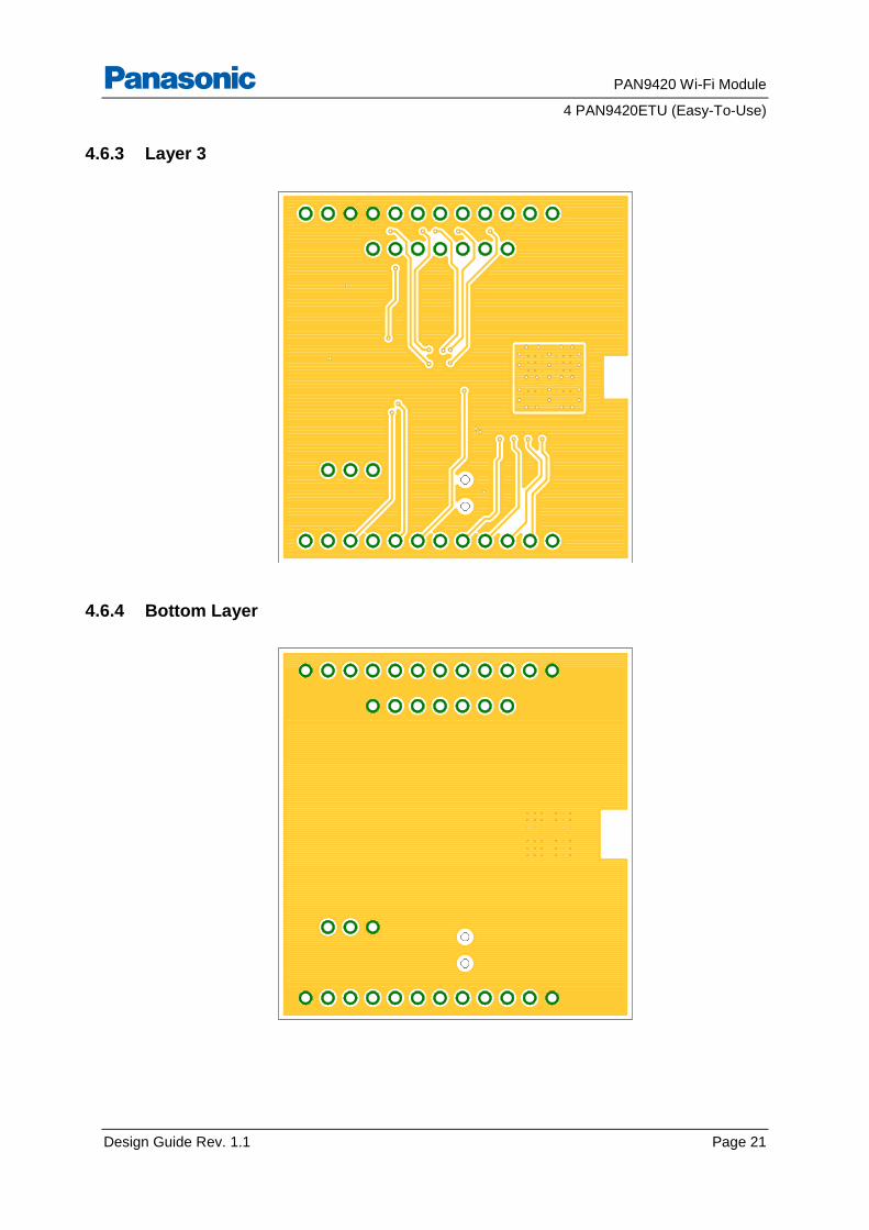
4.6.3 Layer 3
4.6.4 Bottom Layer

PAN9420 Wi-Fi Module
5 PAN9420 Arduino Shield
Design Guide Rev. 1.1 Page 22
5 PAN9420 Arduino Shield
The PAN9420 Arduino Shield (Order-No. ENW49C01AXKF) is a further sample application of
the PAN9420 module. It is designed for mounting on the Arduino Due.
5.1 PAN9420 Arduino Shield Live View

PAN9420 Wi-Fi Module
5 PAN9420 Arduino Shield
Design Guide Rev. 1.1 Page 23
5.2 Functional Blocks
Functional Block Description
A PAN9420 module
B GPIO pins (46 – 49) of the PAN9420 module
C Vcc LED (is active when Vcc is supplied)
D GPIO pins (4, 5) of the PAN9420 module
E IP connectivity pin (allocated IP)
F Status LED’s
G MCU ready pin
H Wake up 1 pin
K Wake up 0 pin
L JTAG Interface
M Ground pins
N General purpose button connected to Arduino pin A1
O General purpose LED’s connected to Arduino pin PWM2 and PWM3
P Free area for additional circuits
1 2
20
G R E E N
G R E E N
Y E L L O W
R E D
B L U E
W H IT ED
F E
A
B
C G
H
K
L M
N
O P

PAN9420 Wi-Fi Module
5 PAN9420 Arduino Shield
Design Guide Rev. 1.1 Page 24
5.3 Pinning
All pins with grey letter are not used for this Arduino shield.
5.4 Part Placement
1 2
20
G R E E N
G R E E N
Y E L L O W
R E D
B L U E
W H IT E
R 5
R 6
L E D 1
L E D 2
R 7
R 8
L E D 3
L E D 4
R 1 3
R 1 4
R 1 5
R 1 6
C 4
R 1 2
R 2
C 1
R 1 L E D 5
C 2
S V 1
R 4
R 9
R 1 1
R1
7
R1
8
R1
9
R2
0
L E D 6 R 2 1
JP 1JP 2
JP 3 JP 4 JP 5
JP 6
JP 7
JP 8
JP 9
JP 1 0 JP 1 1 JP 1 2 JP 1 3 JP 1 4 JP 1 5 JP 1 6 JP 1 7
JP 1 8M O D 2
R 3
R 1 0
L E D 7
L E D 8
S 1
R2
2

PAN9420 Wi-Fi Module
5 PAN9420 Arduino Shield
Design Guide Rev. 1.1 Page 25
5.5 Schematic
+3V3
680
680
GREEN
YELLO
W
680
680
RED
BLU
E
+3V3
10k10k10k10k
0.1
10k
+3V3
+3V3
10k
0.1
680
WHITE
10µ
+3V3
10k
10k
10k
680
680
680
680
GREEN
+3V3
680
680
+3V3
680
LG
_T679-E
1F1-1
LG
_T679-E
1F1-1 S
KH
MPSE010
10k
5V
5V@
2
D22
D22
D24
D24
D26
D26
D28
D28
D30
D30
D32
D32
D34
D34
D36
D36
D38
D38
D40
D40
D42
D42
D44
D44
D46
D46
D48
D48
D50
D50
D52
D52
GN
DG
ND
@4
GN
DG
ND
@5
D53
D53
D51
D51
D49
D49
D47
D47
D45
D45
D43
D43
D41
D41
D39
D39
D37
D37
D35
D35
D33
D33
D31
D31
D29
D29
D27
D27
D25
D25
D23
D23
5V
5V@
3A0
D54
A1
D55
A2
D56
A3
D57
A4
D58
A5
D59
A6
D60
A7
D61
A8
D62
A9
D63
A10
D64
A11
D65
DAC0
D66
DAC1
D67
CAN
RX
D68
CAN
TX
D69
PW
M7
D7
PW
M6
D6
PW
M5
D5
PW
M4
D4/D
87
PW
M3
D3
PW
M2
D2
TX0
D1
RX0
D0
TX3
D14
RX3
D15
TX2
D16
RX2
D17
TX1
D18
RX1
D19
SD
AD
20
SCL
D21
N.C
.N
.C.
IOREF
IOREF
RESET
RESET
3V3
3V3
5V
5V@
1
GN
DG
ND
@1
GN
DG
ND
@2
VIN
VIN
SCL1
D71
SD
A1
D70
AREF
AREF
GN
DG
ND
@3
PW
M13
D13
PW
M12
D12
PW
M11
D11
PW
M10
D10/D
77
PW
M9
D9
PW
M8
D8
R5
R6
LED
1
LED
2R7
R8
LED
3
LED
4
R13R14R15R16
C4
R12
R2
C1
R1
LED5
C2
SV1
1 3 5 7 911
13
15
17
19
2 4 6 8 10
12
14
16
18
20
R4
R9
R11
R17
R18
R19
R20
LED6R21
1 JP1
1 JP2
1 JP3
1 JP4
1 JP5
1 JP6
1 JP7
1 JP8
1 JP9
1 JP10
1 JP11
1 JP12
1 JP13
1 JP14
1 JP15
1 JP16
1 JP17
1 JP18
MO
D2 GND
1
GND14
GND15
GND17
GND18
GND19
GND20
GND21
GND22
GND23
GND24
GND25
GND36
GNDF3
GNDF4
GNDF5
GNDD3
GND_THERMOT1
GND_THERMOT2
GND_THERMOT3
GND_THERMOT4
GPIO
[4]_
/_I2
C0_SD
A2
GPIO
[5]_
/_I2
C0_SCL
3
3.3V7
3.3V8
UART1_CTSN
9U
ART1_RTSN
10
UART1_TXD
11
UART1_RXD
12
RF
16
W_STATU
S_LED
26
UART0_TXD
27
UART0_RXD
28
GPIO
[16]_
/_BO
OT1
5
GPIO
[27]_
/_BO
OT2
6
GPIO
[46]_
/_SSP2_CLK
32
GPIO
[47]_
/_SSP2_FRM
31
STATU
S_LED
335
STATU
S_LED
234
STATU
S_LED
133
RESETN
37
WAKE_U
P0
38
GPIO
[48]_
/_SSP2_TXD
30
MCU
_READ
Y41
FACTO
RY_RESET
42
WAKE_U
P1
C3
QSPI_
CLK
C4
QSPI_
D3
C5
TD
ID
1
TRSTN
D2
QSPI_
D0
D4
QSPI_
D1
D5
TD
OE1
TCK
E2
TM
SE3
QSPI_
D2
E4
QSPI_
CS
E5
GPIO
[49]_
/_SSP2_RXD
29
SPD
T_U
2A5
SPD
T_U
1A4
R3
R10
LED
7
LED
8
S1
R22
UART1_TXD
UART1_TXD
UART1_RXD
UART1_RXD
IP_CO
NN
IP_CO
NN
RESETN
RESETN
RESETN
MO
D_TD
I
MO
D_TD
I
MO
D_TD
O
MO
D_TD
O
MO
D_TCK
MO
D_TCK
MO
D_TM
S
MO
D_TM
S
MO
D_TRSTN
MO
D_TRSTN
MCU
_READ
Y
UART0_RXD
UART0_RXD
UART0_TXD
UART0_TXD
JTAG
IN
TERFACE
Data
Com
mand
Sta
tus
Led D
x
PW
M
Date
:31.0
8.2
018 1
5:4
4Sheet:
1/1R
EV:
TIT
LE:
Docu
ment
Num
ber:
PAN
9420_Ard
uin
oShie
ld

PAN9420 Wi-Fi Module
5 PAN9420 Arduino Shield
Design Guide Rev. 1.1 Page 26
5.6 PCB Layout
5.6.1 Top Layer
5.6.2 Bottom Layer

PAN9420 Wi-Fi Module
6 Life Support Policy
Design Guide Rev. 1.1 Page 27
6 Life Support Policy
This Panasonic Industrial Devices Europe GmbH product is not designed for use in life support
appliances, devices, or systems where malfunction can reasonably be expected to result in a
significant personal injury to the user, or as a critical component in any life support device or
system whose failure to perform can be reasonably expected to cause the failure of the life
support device or system, or to affect its safety or effectiveness.
Panasonic customers using or selling these products for use in such applications do so at their
own risk and agree to fully indemnify Panasonic Industrial Devices Europe GmbH for any
damages resulting.

PAN9420 Wi-Fi Module
7 Appendix
Design Guide Rev. 1.1 Page 28
7 Appendix
7.1 Ordering Information
Variants and Versions
Order Number Brand Name Description MOQ1
ENW49C01A3KF PAN9420 Fully embedded stand alone Wi Fi module IEEE 802.11
b/g/n
Regulatory notice: FCC/IC for US and for Canada
Supported channel: Channel 1~11, 2412~2462 MHz
500
ENW49C02A3KF PAN9420 Fully embedded stand alone Wi Fi module IEEE 802.11
b/g/n
Regulatory notice: ETSI for EU and other
Supported channel: Channel 1~13, 2412~2472 MHz
500
ENW49C01AZKF PAN9420ETU PAN9420 Easy-To-Use pin-header board with the
module ENW49C01A3KF
1
ENW49C01AYKF PAN9420-KIT PAN9420 Evaluation Kit. It contains the following parts:
• PAN9420 Mother Board
• PAN9420ETU
• USB Type-B cable
1
ENW49C01AXKF PAN9420
Arduino Shield
Arduino Shield with the module ENW49C01A3KF for
the Arduino Due Board
1
1 Abbreviation for Minimum Order Quantity (MOQ). Samples for evaluation can be delivered at any quantity via the distribution channels.

PAN9420 Wi-Fi Module
7 Appendix
Design Guide Rev. 1.1 Page 29
7.2 Contact Details
7.2.1 Contact Us
Please contact your local Panasonic Sales office for details on additional product options and
services:
For Panasonic Sales assistance in the EU, visit
https://eu.industrial.panasonic.com/about-us/contact-us
Email: [email protected]
For Panasonic Sales assistance in North America, visit the Panasonic website
“Sales & Support” to find assistance near you at
https://na.industrial.panasonic.com/distributors
Please visit the Panasonic Wireless Technical Forum to submit a question at
https://forum.na.industrial.panasonic.com
7.2.2 Product Information
Please refer to the Panasonic Wireless Connectivity website for further information on our
products and related documents:
For complete Panasonic product details in the EU, visit
http://pideu.panasonic.de/products/wireless-modules.html
For complete Panasonic product details in North America, visit
http://www.panasonic.com/rfmodules