lt3752/lt3752-1 - active clamp synchronous forward ...€¦ · housekeeping controller the lt ......
TRANSCRIPT

LT3752/LT3752-1
13752fb
For more information www.linear.com/LT3752
TYPICAL APPLICATION
FEATURES DESCRIPTION
Active Clamp Synchronous Forward Controllers with Internal
Housekeeping Controller
The LT®3752/LT3752-1 are current mode PWM controllers optimized for an active clamp forward converter topology. A DC/DC housekeeping controller is included for improved efficiency and performance. The LT3752 allows operation up to 100V input and the LT3752-1 is optimized for ap-plications with input voltages greater than 100V.
A programmable volt-second clamp allows primary switch duty cycles above 50% for high switch, transformer and rectifier utilization. Active clamp control reduces switch voltage stress and increases efficiency. A synchronous output is available for controlling secondary side syn-chronous rectification.
The LT3752/LT3752-1 are available in a 38-lead plastic TSSOP package with missing pins for high voltage spacings.
18V to 72V, 12V/12.5A, 150W Active Clamp Isolated Forward Converter
APPLICATIONS
n Input Voltage Range: LT3752: 6.5V to 100V, LT3752-1:Limited Only by External Componentsn Internal Housekeeping DC/DC Controllern Programmable Volt-Second Clampn High Efficiency Control: Active Clamp, Synchronous Rectification, Programmable Delaysn Short-Circuit (Hiccup Mode) Overcurrent Protectionn Programmable Soft-Start/Stopn Programmable OVLO and UVLO with Hysteresisn Programmable Frequency (100kHz to 500kHz)n Synchronizable to an External Clock
n Offline and HV Car Battery Isolated Power Suppliesn 48V Telecommunication Isolated Power Suppliesn Industrial, Automotive and Military Systems L, LT, LTC, LTM, Linear Technology and the Linear logo are registered trademarks of Linear
Technology Corporation. All other trademarks are the property of their respective owners.
49.9k
22.6k
1.82k
7.32k
34k
71.5k
31.6k
100k100k
2.8k
10k
560Ω
3.16k
100k
VAUX
VAUX
SYNC
VIN
GND
FBLT8311PGOOD
2k0.006Ω
10k0.15Ω499Ω
2.2µF2.2µF
INTVCC VAUX
ZVN4525E6
100Ω
1.1k
1.2k 2.2nF EFFICIENCY: 94% AT 48VIN/10AOUT
0.33µF
22nF
22nF
4.7µF
2.2µF
22µF16V×2
VOUT12V12.5A
470µF16V
4.7µF
220nF
3752 TA01
68pF
4.7nF
220pF
1µF
T AO
T AS
T OS
T BLN
KIV
SEC
RT SS1
SS2
HCOM
P
FB COM
P
OPTO
INTV
CC
TIM
ER
SS COM
PCS
P
PMOD
E
INTVCCINTVCC
SOUT
ISENSEN
ISENSEP
OUTVIN AOUTHISENSEHOUT
OC
5.9k
100k
UVLO_VSEC
LT3752
SYNC
100nF
15nFSi2325DS
4:4
BSC077N12NS3FDMS86101
BSC077N12NS3
499k
13.7k
6.8µH
100k
11.3k
CSNFG F SW C G
C SW
100Ω 100Ω
+
••
•••
•
•4.7µF100V
×3
VIN18V TO 72V
GND
OVLO
HFB
68pF
LT3752/LT3752-1
23752fb
For more information www.linear.com/LT3752
TABLE OF CONTENTSFeatures ..................................................... 1Applications ................................................ 1Typical Application ........................................ 1Description.................................................. 1Table of Contents .......................................... 2Absolute Maximum Ratings .............................. 3Order Information .......................................... 3Pin Configuration .......................................... 3Electrical Characteristics ................................. 4Pin Functions .............................................. 13Block Diagram ............................................. 15Timing Diagrams ......................................... 16Operation................................................... 19
Introduction ....................................................... 19LT3752 Part Start-Up ......................................... 19LT3752-1 Part Start-Up ...................................... 19
Applications Information ................................ 21Programming System Input Undervoltage Lockout (UVLO) Threshold and Hysteresis ...................... 21Soft-Stop Shutdown ........................................... 21Micropower Shutdown ....................................... 21Programming System Input Overvoltage Lockout (OVLO) Threshold ............................................... 21LT3752-1 Micropower Start-Up from High System Input Voltages ....................................................22Programming Switching Frequency ....................23Synchronizing to an External Clock ....................23INTVCC Regulator Bypassing and Operation ...... 24
HOUSEKEEPING CONTROLLER .............................. 24Housekeeping: Operation ....................................25Housekeeping: Soft-Start/Shutdown ..................25Housekeeping: Programming Output Voltage .....25Housekeeping: Programming Cycle-by-Cycle Peak Inductor Current and Slope Compensation .........25Housekeeping: Adaptive Leading Edge Blanking .26Housekeeping: Overcurrent Hiccup Mode ...........26Housekeeping: Output Overvoltage and Power Good ..................................................................26Housekeeping: Transformer Turns Ratio and Leakage Inductance ............................................26Housekeeping: Operating Without This Supply ...27
FORWARD CONTROLLER .......................................27Adaptive Leading Edge Blanking Plus Programmable Extended Blanking......................27Current Sensing and Programmable Slope Compensation ....................................................28Overcurrent: Hiccup Mode ..................................28Programming Maximum Duty Cycle Clamp: DVSEC (Volt-Second Clamp) ..........................................29DVSEC Open Loop Control: No Opto-Coupler, Error Amplifier or Reference ........................................30RIVSEC: Open Pin Detection Provides Safety .......30Transformer Reset: Active Clamp Technique .....30LO Side Active Clamp Topology (LT3752) ...........32HI Side Active Clamp Topology (LT3752-1) .........33Active Clamp Capacitor Value and Voltage Ripple ....................................................33Active Clamp MOSFET Selection ........................34Programming Active Clamp Switch Timing: AOUT to OUT (tAO) and OUT to AOUT (tOA) Delays .......35Programming Synchronous Rectifier Timing: SOUT to OUT (tSO) and OUT to SOUT (tOS) Delays .................................................................35Soft-Start (SS1, SS2) .........................................36Soft-Stop (SS1) ..................................................36Hard-Stop (SS1, SS2) ......................................... 37OUT, AOUT, SOUT Pulse-Skipping Mode ............ 37AOUT Timeout ....................................................38Main Transformer Selection ...............................38Primary-Side Power MOSFET Selection .............40Synchronous Control (SOUT) .............................40Output Inductor Value ......................................... 41Output Capacitor Selection ................................. 41Input Capacitor Selection ................................... 41PCB Layout / Thermal Guidelines ......................42
Typical Applications ...................................... 44Package Description ..................................... 50Revision History .......................................... 51Typical Application ....................................... 52Related Parts .............................................. 52

LT3752/LT3752-1
33752fb
For more information www.linear.com/LT3752
PIN CONFIGURATIONABSOLUTE MAXIMUM RATINGS
VIN (LT3752) ...........................................................100VUVLO_VSEC, OVLO ....................................................20VVIN (LT3752-1) .................................................16V, 8mAINTVCC, SS2..............................................................16VFB, SYNC ....................................................................6VSS1, COMP, HCOMP, HFB, RT .....................................3VISENSEP, ISENSEN, OC, HISENSE ................................0.35VIVSEC ..................................................................–250µAOperating Junction Temperature Range (Notes 2, 3) LT3752EFE, LT3752EFE-1 .................. –40°C to 125°C LT3752IFE, LT3752IFE-1 .................... –40°C to 125°C LT3752HFE, LT3752HFE-1 ................. –40°C to 150°C LT3752MPFE, LT3752MPFE-1 ............ –55°C to 150°CStorage Temperature Range .................. –65°C to 150°C Lead Temperature (Soldering, 10 Sec) .................. 300°C
(Note 1)
1
2
3
4
5
6
7
8
9
10
11
12
13
14
15
16
17
18
19
TOP VIEW
FE PACKAGEVARIATION: FE38(31)
38-LEAD PLASTIC TSSOP
38
37
36
34
32
30
28
26
24
22
21
20
HFB
HCOMP
RT
FB
COMP
SYNC
SS1
IVSEC
UNLO_VSEC
OVLO
TAO
TAS
TOS
TBLNK
NC
NC
SS2
GND
PGND
PGND
NC
HISENSE
HOUT
AOUT
SOUT
VIN
INTVCC
OUT
OC
ISENSEP
ISENSEN
39PGNDGND
θJA = 25°C/W EXPOSED PAD (PIN 39) IS PGND AND GND, MUST BE SOLDERED TO PCB
ORDER INFORMATIONLEAD FREE FINISH TAPE AND REEL PART MARKING* PACKAGE DESCRIPTION TEMPERATURE RANGE
LT3752EFE#PBF LT3752EFE#TRPBF LT3752FE 38-Lead Plastic TSSOP –40°C to 125°C
LT3752IFE#PBF LT3752IFE#TRPBF LT3752FE 38-Lead Plastic TSSOP –40°C to 125°C
LT3752HFE#PBF LT3752HFE#TRPBF LT3752FE 38-Lead Plastic TSSOP –40°C to 150°C
LT3752MPFE#PBF LT3752MPFE#TRPBF LT3752FE 38-Lead Plastic TSSOP –55°C to 150°C
LT3752EFE-1#PBF LT3752EFE-1#TRPBF LT3752FE-1 38-Lead Plastic TSSOP –40°C to 125°C
LT3752IFE-1#PBF LT3752IFE-1#TRPBF LT3752FE-1 38-Lead Plastic TSSOP –40°C to 125°C
LT3752HFE-1#PBF LT3752HFE-1#TRPBF LT3752FE-1 38-Lead Plastic TSSOP –40°C to 150°C
LT3752MPFE-1#PBF LT3752MPFE-1#TRPBF LT3752FE-1 38-Lead Plastic TSSOP –55°C to 150°C
Consult LTC Marketing for parts specified with wider operating temperature ranges. *The temperature grade is identified by a label on the shipping container.Consult LTC Marketing for information on nonstandard lead based finish parts.For more information on lead free part marking, go to: http://www.linear.com/leadfree/ For more information on tape and reel specifications, go to: http://www.linear.com/tapeandreel/

LT3752/LT3752-1
43752fb
For more information www.linear.com/LT3752
ELECTRICAL CHARACTERISTICS The l denotes the specifications which apply over the full operating temperature range, otherwise specifications are at TA = 25°C. VIN = 12V, UVLO_VSEC = 2.5V.
PARAMETER CONDITIONS MIN TYP MAX UNITSOperational Input Voltage (LT3752) l 6.5 100 VOperational Input Voltage (LT3752-1) l 10.5 16 VVIN(ON) (LT3752) l 5.8 6.4 VVIN(OFF) (LT3752) 5.5 5.9 VVIN(ON/OFF) Hysteresis (LT3752) l 0.1 0.3 0.5 VVIN(ON) (LT3752-1) l 9.5 10.4 VVIN(OFF) (LT3752-1) 7.6 VVIN(ON/OFF) Hysteresis (LT3752-1) l 1.61 1.9 2.19 VVIN Start-Up Current (LT3752-1) (Notes 6, 7) l 170 265 µAVIN Quiescent Current (Housekeeping Controller Only) (LT3752)
HCOMP = 1V (Housekeeping Not Switching), HFB = 0.85V
l 4 6.2 mA
VIN Quiescent Current (Housekeeping Controller Only) (LT3752-1)
HCOMP = 1V (Housekeeping Not Switching), HFB = 0.85V
l 3 4.6 mA
VIN Quiescent Current (Housekeeping Controller + Forward Controller)
HCOMP = 1V (Housekeeping Not Switching), HFB = 1.35V, FB = 1.5V (Main Loop Not Switching)
7.5 9.5 mA
UVLO_VSEC Micropower Threshold (VSD) IVIN < 20µA l 0.2 0.4 0.6 VVIN Shutdown Current (Micropower) UVLO_VSEC = 0.2V 20 40 µAUVLO_VSEC Threshold (VSYS_UV) l 1.180 1.250 1.320 VVIN Shutdown Current (After Soft-Stop) UVLO_VSEC = 1V 165 220 µAUVLO_VSEC (ON) Current UVLO_VSEC = VSYS_UV + 50mV 0 µAUVLO_VSEC (OFF) Current Hysteresis Current With One-Shot Communication Current
UVLO_VSEC = VSYS_UV – 50mV (Note 15)
l
4.0
5
25
6.0
µA µA
OVLO (Rising) (No Switching, Reset SS1) l 1.220 1.250 1.280 VOVLO (Falling) (Restart SS1) 1.215 VOVLO Hysteresis l 23 35 47 mVOVLO Pin Current (Note 10) OVLO = 0V
OVLO = 1.5V (SS1 = 2.7V) OVLO = 1.5V (SS1 = 1.0V)
5 0.9 5
100
100
nA mA nA
Oscillator (Forward Controller: OUT, SOUT, AOUT)Frequency: fOSC = 100kHz RT = 82.5k 94 100 106 kHzFrequency: fOSC = 300kHz RT = 24.9k l 279 300 321 kHzFrequency: fOSC = 500kHz RT = 14k 470 500 530 kHzfOSC Line Regulation RT = 24.9k
6.5V < VIN < 100V (LT3752) 10.5V < VIN < 16V (LT3752-1)
0.05 0.05
0.1 0.1
%/V %/V
Frequency and DVSEC Foldback Ratio (LT3752) (Fold) SS1 = VSSACT + 25mV, SS2 = 2.7V 4Frequency and DVSEC Foldback Ratio (LT3752-1) (Fold) SS1 = VSS1ACT + 25mV, SS2 = 2.7V 2SYNC Input High Threshold (Note 4) l 1.2 1.8 VSYNC Input Low Threshold (Note 4) l 0.6 1.025 VSYNC Pin Current SYNC = 6V 75 µASYNC Frequency/Programmed fOSC 1.0 1.25 kHz/kHzLinear Regulator (INTVCC) (LT3752)INTVCC Regulation Voltage 6.6 7 7.2 VDropout (VIN-INTVCC) VIN = 6.5V, IINTVCC = 10mA 0.8 VINTVCC UVLO(+) (Start Switching) 4.75 5 V

LT3752/LT3752-1
53752fb
For more information www.linear.com/LT3752
ELECTRICAL CHARACTERISTICS The l denotes the specifications which apply over the full operating temperature range, otherwise specifications are at TA = 25°C. VIN = 12V, UVLO_VSEC = 2.5V.
PARAMETER CONDITIONS MIN TYP MAX UNITSINTVCC UVLO(–) (Stop Switching) 4.6 4.85 VINTVCC UVLO Hysteresis 0.075 0.15 0.24 VLinear Regulator (INTVCC) (LT3752-1)INTVCC Regulation Voltage 9.4 10 10.4 VDropout (VIN-INTVCC) VIN = 8.75V, IINTVCC = 10mA 0.6 VINTVCC UVLO(+) (Start Switching) 7 7.4 VINTVCC UVLO(–) (Stop Switching) 6.8 7.2 VINTVCC UVLO Hysteresis 0.1 0.2 0.3 VLinear Regulator (INTVCC) (LT3752/LT3752-1)INTVCC OVLO(+) (Stop Switching) 15.9 16.5 17.2 VINTVCC OVLO(–) (Start Switching) 15.4 16 16.7 VINTVCC OVLO Hysteresis 0.38 0.5 0.67 VINTVCC Current Limit INTVCC = 0V
INTVCC = 5.75V (LT3752) INTVCC = 8.75V (LT3752-1)
l
l
17 35 35
23 50 50
29 60 60
mA mA mA
Error AmplifierFB Reference Voltage l 1.220 1.250 1.275 VFB Line Reg 6.5V < VIN < 100V (LT3752)
10.5V < VIN < 16V (LT3752-1)0.1 0.1
0.3 0.3
mV/V mV/V
FB Load Reg COMP_SW – 0.1V < COMP < COMP_VOH – 0.1V 0.1 0.3 mV/VFB Input Bias Current (Note 10) 50 200 nAOpen-Loop Voltage Gain 85 dBUnity-Gain Bandwidth (Note 8) 2.5 MHzCOMP Source Current FB = 1V, COMP = 1.75V (Note 10) 6 11 mACOMP Sink Current FB = 1.5V, COMP = 1.75V 6.5 11.5 mACOMP Output High Clamp FB = 1V 2.6 VCOMP Switching Threshold 1.25 VCurrent Sense (Main Loop)ISENSEP Maximum Threshold FB = 1V, OC = 0V 180 220 260 mVCOMP Current Mode Gain ∆VCOMP/∆VISENSEP 6.1 V/V
ISENSEP Input Current (D = 0%) (Note 10) 2 µAISENSEP Input Current (D = 80%) (Note 10) 33 µAISENSEN Input Current FB = 1.5V (COMP Open) (Note 10)
FB = 1V (COMP Open) (Note 10)20 90
30 135
µA µA
OC Overcurrent Threshold l 82.5 96 107.5 mVOC Input Current 200 500 nAAOUT Driver (Active Clamp Switch Control) (LT3752 External PMOS; LT3752-1 External NMOS)AOUT Rise Time CL = 1nF (Note 5), INTVCC = 12V 23 nsAOUT Fall Time CL = 1nF (Note 5), INTVCC = 12V 19 nsAOUT Low Level 0.1 VAOUT High Level INTVCC = 12V 11.9 VAOUT High Level in Shutdown (LT3752) UVLO_VSEC = 0V, INTVCC = 8V, IAOUT = 1mA Out
of the Pin7.8 V
AOUT Low Level in Shutdown (LT3752-1) UVLO_VSEC = 0V, INTVCC = 12V, IAOUT = 1mA Into the Pin
0.25 V

LT3752/LT3752-1
63752fb
For more information www.linear.com/LT3752
ELECTRICAL CHARACTERISTICS The l denotes the specifications which apply over the full operating temperature range, otherwise specifications are at TA = 25°C. VIN = 12V, UVLO_VSEC = 2.5V.
PARAMETER CONDITIONS MIN TYP MAX UNITSAOUT Edge to OUT (Rise): (tAO) CSOUT = 1nF, COUT = 3.3nF, INTVCC = 12V
RTAO = 44.2k RTAO = 73.2k (Note 11)
168 253
218 328
268 403
ns ns
OUT (Fall) to AOUT Edge: (tOA) CSOUT = 1nF, COUT = 3.3nF, INTVCC = 12V RTAO = 44.2k RTAO = 73.2k (Note 12)
150 214
196 295
250 376
ns ns
SOUT Driver (Synchronous Rectification Control)SOUT Rise Time COUT = 1nF, INTVCC = 12V (Note 5) 21 nsSOUT Fall Time COUT = 1nF, INTVCC = 12V (Note 5) 19 nsSOUT Low Level 0.1 VSOUT High Level INTVCC = 12V 11.9 VSOUT High Level in Shutdown UVLO_VSEC = 0V, INTVCC = 8V, ISOUT = 1mA Out
of the Pin7.8 V
AOUT Edge to SOUT (Fall): (tAS) CAOUT = CSOUT = 1nF, INTVCC = 12V RTAS = 44.2k (Note 13) RTAS = 73.2k
168 253
218 328
268 403
ns ns
SOUT (Fall) to OUT (Rise): (tSO = tAO – tAS) CSOUT = 1nF, COUT = 3.3nF, INTVCC = 12V RTAO = 73.2k, RTAS = 44.2k (Notes 11, 13) RTAO = 44.2k, RTAS = 73.2k
70
–70
110
–110
132
–132
ns ns
OUT (Fall) to SOUT (Rise): (tOS) CSOUT = 1nF, COUT = 3.3nF, INTVCC = 12V RTOS = 14.7k RTOS = 44.2k (Note 14)
52
102
68
133
84
164
ns ns
OUT Driver (Main Power Switch Control)
OUT Rise Time COUT = 3.3nF, INTVCC = 12V (Note 5) 19 ns
OUT Fall Time COUT = 3.3nF, INTVCC = 12V (Note 5) 20 ns
OUT Low Level 0.1 V
OUT High Level INTVCC = 12V 11.9 V
OUT Low Level in Shutdown UVLO_VSEC = 0V, INTVCC = 8V, IOUT = 1mA Into the Pin
0.25 V
OUT (Volt-Sec) Max Duty Cycle Clamp DVSEC (1 • System Input (Min)) × 100 DVSEC (2 • System Input (Min)) × 100 DVSEC (4 • System Input (Min)) × 100
RT = 24.9k, RIVSEC = 51.1k, FB = 1V, SS1 = 2.7V UVLO_VSEC = 1.25V UVLO_VSEC = 2.50V UVLO_VSEC = 5.00V
68.5 34.3 17.5
72.5 36.5 18.6
76.2 38.7 19.7
% % %
OUT Minimum ON Time COUT = 3.3nF, INTVCC = 12V (Note 9) RTBLNK = 14.7k RTBLNK = 73.2k (Note 16)
325 454
ns ns
SS1 Pin (Soft-Start: Frequency and DVSEC) (Soft-Stop: COMP Pin, Frequency and DVSEC)
SS1 Reset Threshold (VSS1(RTH)) 150 mV
SS1 Active Threshold (VSS1(ACT)) (Allow Switching) 1.25 V
SS1 Charge Current (Soft-Start) SS1 = 1.5V (Note 10) 7 11.5 16 µA
SS1 Discharge Current (Soft-Stop) SS1 = 1V, UVLO_VSEC = VSYS_UV – 50mV 6.4 10.5 14.6 µA
SS1 Discharge Current (Hard Stop) OC > OC Threshold INTVCC < INTVCC UVLO(–) OVLO > OVLO(+)
SS1 = 1V 0.9 0.9 0.9
mA mA mA
SS2 Pin (Soft-Start: Comp Pin)
SS2 Discharge Current SS1 < VSS(ACT), SS2 = 2.5V 2.8 mA
SS2 Charge Current SS1 > VSS(ACT), SS2 = 1.5V 11 21 28 µA

LT3752/LT3752-1
73752fb
For more information www.linear.com/LT3752
PARAMETER CONDITIONS MIN TYP MAX UNITSError Amplifier (Housekeeping Controller)
HFB Reference Voltage 0.90 1.000 1.10 V
HFB Line Reg 6.5V < VIN < 100V (LT3752) 10.5V < VIN < 16V (LT3752-1)
0.1 0.1
mV/V mV/V
HFB Load Reg HCOMP VSW – 0.1V < HCOMP < HCOMP VOH – 0.1V
–6 mV/V
HFB Input Bias Current HFB = 1.1V (Note 10) 85 170 nA
Transconductance ∆IHCOMP ±5µA 250 µS
Voltage Gain 175 V/V
Power Good(+) (HFB Level) 0.96 V
Power Good(–) (HFB Level) 0.92 V
HFB OVLO(+) (Disable HOUT Switching) 1.206 V
HFB OVLO(–) (Enable Housekeeping Operation) 1.150 V
HCOMP Source Current HCOMP = 1.75V (Note 10) 11 15 19 µA
HCOMP Sink Current HCOMP = 1.75V 13 18 23 µA
HCOMP Output High Clamp 2.9 V
HCOMP Switching Threshold 1.28 V
Current Sense (Housekeeping Controller)
HISENSE Peak Current Threshold HFB = 0.8V 69 79 86.5 mV
HCOMP Current Mode Gain ∆VHCOMP/∆VHISENSE 9.1 V/V
HISENSE Input Current (D = 0%) HISENSE Input Current (D = 80%)
(Note 10) 2 52
µA µA
HISENSE Overcurrent Threshold 84.6 98 105.4 mV
HOUT Driver (Housekeeping Controller)
HOUT Rise Time CL = 1nF (Note 5), INTVCC = 12V 13 ns
HOUT Fall Time CL = 1nF (Note 5), INTVCC = 12V 12 ns
HOUT Low Level 0.1 V
HOUT High Level LT3752 LT3752-1
INTVCC = 12V
11.9 11.9
V V
HOUT Low Level in Shutdown UVLO_VSEC = 0V, INTVCC = 12V, IHOUT = 1mA Into the Pin
0.25 V
HOUT Maximum Duty Cycle HCOMP = 2.7V, RT = 24.9k 90 95 %
HOUT Minimum ON Time CL = 1nF (Note 9), INTVCC = 12V 350 ns
Soft-Start (HSS) (Housekeeping Controller)
HSS (Internal) Ramp Time (tHSS) HCOMP SW ≥ HCOMP VOH – 0.1V 2.2 4 ms
Oscillator (Housekeeping Controller)
Frequency (fHOUT) (fOSC Folded Back) (LT3752) HFB = 0.8V, RT = 24.9k, SS1 = 0V 55 65 75 kHz
Frequency (fHOUT) (fOSC Folded Back) (LT3752-1) HFB = 0.8V, RT = 24.9k, SS1 = 0V 119 141 163 kHz
Frequency (fHOUT) (Full-Scale fOSC) HFB = 1.15V, HCOMP = 2.7V l 279 300 321 kHz
ELECTRICAL CHARACTERISTICS The l denotes the specifications which apply over the full operating temperature range, otherwise specifications are at TA = 25°C. VIN = 12V, UVLO_VSEC = 2.5V.

LT3752/LT3752-1
83752fb
For more information www.linear.com/LT3752
ELECTRICAL CHARACTERISTICSNote 1: Stresses beyond those listed under Absolute Maximum Ratings may cause permanent damage to the device. Exposure to any Absolute Maximum Rating condition for extended periods may affect device reliability and lifetime.Note 2: The LT3752EFE/LT3752EFE-1 are guaranteed to meet performance specifications from 0°C to 125°C junction temperature. Specifications over the –40°C to 125°C operating junction temperature range are assured by design, characterization and correlation with statistical process controls. The LT3752IFE/LT3752IFE-1 are guaranteed to meet performance specifications from –40°C to 125°C junction temperature. The LT3752HFE/LT3752HFE-1 are guaranteed to meet performance specifications from –40°C to 150°C junction temperature. The LT3752MPFE/LT3752MPFE-1 are tested and guaranteed to meet performance specifications from –55°C to 150°C junction temperature.Note 3: For maximum operating ambient temperature, see the Thermal Calculations section in the Applications Information section.Note 4: SYNC minimum and maximum thresholds are guaranteed by SYNC frequency range test using a clock input with guard banded SYNC levels of 0.7V low level and 1.7V high level.Note 5: Rise and fall times are measured between 10% and 90% of gate driver supply voltage.
Note 6: Guaranteed by correlation to static test.Note 7: VIN start-up current is measured at VIN = VIN(ON) – 0.25V and then scaled by 1.18× to correlate to worst-case VIN current required for part start-up at VIN = VIN(ON).Note 8: Guaranteed by design.Note 9: ON times are measured between rising and falling edges at 50% of gate driver supply voltage.Note 10: Current flows out of pin.Note 11: Guaranteed by correlation to RTAS = 73.2k test.Note 12: tOA timing guaranteed by design based on correlation to measured tAO timing.Note 13: Guaranteed by correlation to RTAO = 44.2k test. Note 14: Guaranteed by correlation to RTOS = 14.7k test.Note 15: A 2µs one-shot of 20µA from the UVLO_VSEC pin allows communication between ICs to begin shutdown (useful when stacking supplies for more power ( = inputs in parallel/outputs in series)). The current is tested in a static test mode. The 2µs one-shot is guaranteed by design. Note 16: Guaranteed by correlation to RTBLNK = 14.7k test.

LT3752/LT3752-1
93752fb
For more information www.linear.com/LT3752
VIN Start-Up and Shutdown Current vs Junction Temperature
VIN(ON), VIN(OFF) Thresholds vs Junction Temperature
VIN Quiescent Current vs Junction Temperature
UVLO_VSEC Turn-On Threshold vs Junction Temperature
UVLO_VSEC Hysteresis Current vs Junction Temperature
HFB PGOOD Thresholds vs Junction Temperature
TYPICAL PERFORMANCE CHARACTERISTICS TA = 25°C, unless otherwise noted.
JUNCTION TEMPERATURE (°C)–75
V IN
CURR
ENT
(µA)
220
180
200
160
140
120
100
80
60
40
20
025 150–25 100
3752 G01
1750 125–50 50 75
LT3752-1 VIN START-UP CURRENT(VIN = VIN_ON)
LT3752/LT3752-1 VIN SHUTDOWN CURRENT(VIN = 12V) UVLO_VSEC = 0.2V
JUNCTION TEMPERATURE (°C)–75
UVLO
_VSE
C TH
RESH
OLD
(V)
1.275
1.270
1.265
1.260
1.255
1.250
1.245
1.240
1.235
1.230
1.22525 150–25 100
3752 G04
1750 125–50 50 75JUNCTION TEMPERATURE (°C)
–75
HFB
PGOO
D TH
RESH
OLDS
(V)
1.20
1.15
1.10
1.05
1.00
0.95
0.90
0.85
0.8025 150–25 100
3752 G06
1750 125–50 50 75
HFB PGOOD (+) = ENABLE FORWARD CONTROLLER CIRCUITRY
HFB PGOOD (–) = DISABLE FORWARD CONTROLLER CIRCUITRY
JUNCTION TEMPERATURE (°C)–75
UVLO
_VSE
C HY
STER
ESIS
CUR
RENT
(µA)
6.0
5.5
5.0
4.5
4.025 150–25 100
3752 G05
1750 125–50 50 75
JUNCTION TEMPERATURE (°C)–75
V IN
I Q (m
A)
8
7
6
5
4
3
2
1
025 150–25 100
3752 G03
1750 125–50 50 75
LT3752: HOUSEKEEPING ONLY(NO SWITCHING)
LT3752/-1: HOUSEKEEPING + FORWARD(NO SWITCHING)
LT3752-1: HOUSEKEEPING ONLY(NO SWITCHING)
JUNCTION TEMPERATURE (°C)–75
V IN
ON/O
FF T
HRES
HOLD
S (V
)
10.0
9.0
9.5
8.5
8.0
7.5
7.0
6.5
6.0
5.5
5.0
4.525 150–25 100
3752 G02
1750 125–50 50 75
LT3752-1 VIN_ON
LT3752-1 VIN_OFF
LT3752 VIN_ON
LT3752 VIN_OFF
HFB Reference Voltage vs Junction Temperature
HFB OVLO Thresholds vs Junction Temperature
JUNCTION TEMPERATURE (°C)–75
HFB
OVLO
THR
ESHO
LDS
(V)
1.30
1.25
1.20
1.15
1.10
1.05
1.0025 150–25 100
3752 G08
1750 125–50 50 75
HFB > OVLO (+) = DISABLE HOUT SWITCHING
HFB < OVLO (–) = ENABLE HOUSEKEEPING OPERATION
JUNCTION TEMPERATURE (°C)–75
HFB
REFE
RENC
E VO
LTAG
E (V
)
1.100
1.075
1.050
1.025
1.000
0.975
0.950
0.925
0.90025 150–25 100
3752 G07
1750 125–50 50 75

LT3752/LT3752-1
103752fb
For more information www.linear.com/LT3752
LT3752-1: INTVCC in Dropout at VIN = 8.75V vs Current, Junction Temperature
LT3752: INTVCC in Dropout at VIN = 6.5V vs Current, Junction Temperature
LT3752: INTVCC UVLO Thresholds vs Junction Temperature
LT3752: INTVCC Regulation Voltage vs Current, Junction Temperature
TYPICAL PERFORMANCE CHARACTERISTICS TA = 25°C, unless otherwise noted.
JUNCTION TEMPERATURE (°C)–75
INTV
CC (V
)
7.0
6.5
6.0
5.5
5.0
3.5
4.5
4.0
3.025 150–25 100
3752 G13
1750 125–50 50 75
ILOAD = 0mAILOAD = 10mAILOAD = 15mAILOAD = 20mA
JUNCTION TEMPERATURE (°C)–75
INTV
CC (V
)
7.00
6.95
6.90
6.85
6.80
6.65
6.75
6.70
6.6025 150–25 100
3752 G15
1750 125–50 50 75
ILOAD = 0mAILOAD = 10mAILOAD = 20mAILOAD = 30mA
VIN = 12V
JUNCTION TEMPERATURE (°C)–75
INTV
CC (V
)
10.0
9.5
9.0
8.5
7.5
8.0
5.5
7.0
6.5
6.0
5.025 150–25 100
3752 G16
1750 125–50 50 75
ILOAD = 0mAILOAD = 10mAILOAD = 15mAILOAD = 20mA
VIN = 12V
HISENSE Peak Current Threshold vs Junction Temperature HISENSE Pin Current vs Duty Cycle
HISENSE Overcurrent (Hiccup Mode) Threshold vs Junction Temperature
Housekeeping Internal Soft-Start Time (HSS) vs Junction Temperature
JUNCTION TEMPERATURE (°C)–75
HISE
NSE
PEAK
CUR
RENT
THR
ESHO
LD (m
V)
85
84
83
82
81
80
79
77
76
78
7525 150–25 100
3752 G09
1750 125–50 50 75DUTY CYCLE (%)
0
HISE
NSE
PIN
CURR
ENT
(µA)
60
50
40
30
10
20
040 9020 70
3752 G10
10030 8010 50 60
TJ = 150°CTJ = 25°CTJ = –55°C
JUNCTION TEMPERATURE (°C)–75
HISE
NSE
OVER
CURR
ENT
THRE
SHOL
D (m
V)
110
105
100
95
85
90
8025 150–25 100
3752 G11
1750 125–50 50 75
JUNCTION TEMPERATURE (°C)–75
HOUS
EKEE
PING
INTE
RNAL
SOF
T-ST
ART
TIM
E (m
s) 3.00
2.75
2.50
2.25
1.75
2.00
1.5025 150–25 100
3752 G12
1750 125–50 50 75JUNCTION TEMPERATURE (°C)
–75
INTV
CC U
VLO
THRE
SHOL
D (V
)
4.85
4.80
4.75
4.70
4.55
4.65
4.60
4.5025 150–25 100
3752 G14
1750 125–50 50 75
INTVCC < UVLO (–): DISABLE SWITCHING
INTVCC > UVLO (+): ENABLE SWITCHING

LT3752/LT3752-1
113752fb
For more information www.linear.com/LT3752
LT3752-1: INTVCC UVLO Thresholds vs Junction Temperature
SS1 Soft-Start/Soft-Stop Pin Currents vs Junction Temperature
SS1 High, Active and Reset Levels vs Junction Temperature
SS2 Soft-Start Charge Current vs Junction Temperature
LT3752-1: INTVCC Regulation Voltage vs Current, Junction Temperature
TYPICAL PERFORMANCE CHARACTERISTICS TA = 25°C, unless otherwise noted.
JUNCTION TEMPERATURE (°C)–75
INTV
CC (V
)
10.009.95
9.909.85
9.80
9.65
9.75
9.70
9.40
9.60
9.559.50
9.45
25 150–25 100
3752 G18
1750 125–50 50 75
ILOAD = 0mAILOAD = 10mAILOAD = 20mAILOAD = 30mA
VIN = 12V
JUNCTION TEMPERATURE (°C)–75
SS2
SOFT
-STA
RT C
HARG
E CU
RREN
T (µ
A)
25
24
23
16
22
21
20
19
18
17
1525 150–25 100
3752 G21
1750 125–50 50 75
SS2 PIN CURRENT* (–1)
JUNCTION TEMPERATURE (°C)–75
SS1
CURR
ENTS
(µA)
14.0
13.5
13.012.5
8.5
12.0
11.5
11.010.5
10.0
9.5
9.0
8.025 150–25 100
3752 G19
1750 125–50 50 75
SS1 SOFT-START: CHARGE CURRENT* (–1)
SS1 SOFT-STOP: DISCHARGE CURRENT
JUNCTION TEMPERATURE (°C)–75
SS1
HIGH
, ACT
IVE
AND
RESE
T LE
VELS
(V)
3.00
2.75
2.502.25
0.25
2.00
1.75
1.501.25
1.00
0.75
0.50
025 150–25 100
3752 G20
1750 125–50 50 75
SS1 ACTIVE LEVEL(ALLOW FORWARD CONVERTER SWITCHING)
SS1 HIGH LEVEL
SS1 RESET LEVEL (RESET SS1 LATCH)
Switching Frequency vs SS1 Pin Voltage
Switching Frequency vs Junction Temperature
JUNCTION TEMPERATURE (°C)–75
SWIT
CHIN
G FR
EQUE
NCY
(kHz
)
325
320
315
280
310
305
300
295
290
285
27525 150–25 100
3752 G23
1750 125–50 50 75
RT = 24.9k
FB Reference Voltage vs Junction Temperature
JUNCTION TEMPERATURE (°C)–75
FB R
EFER
ENCE
VOL
TAGE
(V)
1.30
1.29
1.28
1.21
1.27
1.26
1.25
1.24
1.23
1.22
1.2025 150–25 100
3752 G24
1750 125–50 50 75
JUNCTION TEMPERATURE (°C)–75
INTV
CC U
VLO
THRE
SHOL
DS (V
)
7.20
7.15
7.107.05
6.65
7.00
6.95
6.906.85
6.80
6.75
6.70
6.6025 150–25 100
3752 G17
1750 125–50 50 75
INTVCC < UVLO (–): DISABLE FORWARD CONVERTER SWITCHING
INTVCC > UVLO (+): ENABLE FORWARD CONVERTER SWITCHING
SS1 (V)0
SWIT
CHIN
G FR
EQUE
NCY
(kHz
)
350325300275
25
250225200175150
10075
125
50
01 2.25 2.50.5 1.75
3752 G22
2.750.75 20.25 1.25 1.5
RT = 24.9kLT3752-1f(HOUT)f(OUT)
f(HOUT)LT3752-1
f(HOUT)LT3752
f(OUT)
LT3752f(HOUT)f(OUT)

LT3752/LT3752-1
123752fb
For more information www.linear.com/LT3752
TYPICAL PERFORMANCE CHARACTERISTICS TA = 25°C, unless otherwise noted.
SOUT (Fall) to OUT (Rise) Delay (tSO = tAO – tAS) vs Junction Temperature
OUT (Fall) to SOUT (Rise) Delay (tOS) vs Junction Temperature
JUNCTION TEMPERATURE (°C)–75
t SO
(ns)
160
140
80
60
40
120
100
2025 150–25 100
3752 G32
1750 125–50 50 75
RTOS = 44.2k
RTOS = 14.7k
RTOS = 7.32k
JUNCTION TEMPERATURE (°C)–75
t SO
(ns)
120
80
100
60
–20–40
–60–80
–100
40
20
0
–12025 150–25 100
3752 G31
1750 125–50 50 75
RTAO = 73.2k, RTAS = 44.2k
RTAO = 44.2k, RTAS = 73.2k
ISENSEP Maximum Threshold vs COMP
Extended Blanking Duration vs Junction Temperature
AOUT to SOUT Delay (tAS) vs Junction Temperature
AOUT to OUT Delay (tAO) and OUT to AOUT Delay (tOA) vs Junction Temperature
ISENSEP Maximum Threshold – VSLP vs Duty Cycle (Programming Slope Compensation)
OC Overcurrent (Hiccup Mode) Threshold vs Junction Temperature
JUNCTION TEMPERATURE (°C)–75
OC O
VERC
URRE
NT T
HRES
HOLD
(mV)
110
105
100
85
95
90
8025 150–25 100
3752 G27
1750 125–50 50 75
JUNCTION TEMPERATURE (°C)–75
t AO
AND
t CA
(ns)
340
300
320
280
200
180
160
260
240
220
14025 150–25 100
3752 G29
1750 125–50 50 75
RTAO = 73.2k
tAO
RTAO = 44.2k
tOA
tAO
tOA
COMP (V)1.2
I SEN
SEP
THRE
SHOL
D (m
V)
240
220
200
20
180
160
140120
60
100
80
40
02.42.2
3752 G25
2.61.61.4 1.8 2
OC THRESHOLD
DUTY CYCLE (%)0
I SEN
SEP
MAX
IMUM
THR
ESHO
LD -
VSLO
PE (V
) 240
220
200
180
160
1409080
3752 G26
1002010 30 40 50 60 70
RISLP = 0Ω
VSLP = I(ISENSEP) • RISLP
RISLP = 1.5kΩ
RISLP = 2kΩ
JUNCTION TEMPERATURE (°C)–75
t AS
(ns)
340
300
320
280
200
180
160
260
240
220
14025 150–25 100
3752 G30
1750 125–50 50 75
RTAS = 73.2k
RTAS = 44.2k
JUNCTION TEMPERATURE (°C)–75
EXTE
NDED
BLA
NKIN
G DU
RATI
ON (n
s)
220
200
180
100
80
160
140
120
6025 150–25 100
3752 G28
1750 125–50 50 75
RTBLNK = 73.2k
RTBLNK = 14.7k

LT3752/LT3752-1
133752fb
For more information www.linear.com/LT3752
TYPICAL PERFORMANCE CHARACTERISTICS TA = 25°C, unless otherwise noted.
Required RIVSEC vs Switching Frequency (for DVSEC × 100 = 72.5%, UVLO_VSEC = 1.25V)
OUT Pin Rise/Fall Times vs OUT Pin Load Capacitance
OUT Maximum Duty Cycle Clamp (DVSEC) vs UVLO_VSEC
SWITCHING FREQUENCY (kHz)100
PROG
RAM
MED
RIV
SEC
(k)
160
140
80
60
40
20
120
100
0250 450400
3752 G34
500200150 300 350OUT PIN LOAD CAPACITANCE (nF)
0
OUT
PIN
RISE
/FAL
L TI
MES
(ns)
60
50
30
20
10
40
03 8 97
3752 G35
1021 4 65
INTVCC = 12V(OVERDRIVEN FROMHOUSEKEEPING SUPPLY)
UVLO_VSEC (V)0
IDVS
EC ×
100
(%)
80
70
40
30
20
10
60
50
03.75 8.757.5
3752 G33
102.51.25 5 6.25
VIN = 12VRT = 24.9k (300kHz)RIVSEC = 51.1k
PIN FUNCTIONSHFB (Pin 1): Housekeeping Supply Error Amplifier Inverting Input.
HCOMP (Pin 2): Housekeeping Supply Error Amplifier Output and Compensation Pin.
RT (Pin 3): A resistor to ground programs switching frequency.
FB (Pin 4): Error Amplifier Inverting Input.
COMP (Pin 5): Error Amplifier Output. Allows various compensation networks for nonisolated applications.
SYNC (Pin 6): Allows synchronization of internal oscillator to an external clock. fSYNC equal to fOSC allowed.
SS1 (Pin 7): Capacitor controls soft-start/stop of switch-ing frequency and volt-second clamp. During soft-stop it also controls the COMP pin.
IVSEC (Pin 8): Resistor Programs OUT Pin Maximum Duty Cycle Clamp (DVSEC). This clamp moves inversely proportional to system input voltage to provide a volt-second clamp.
UVLO_VSEC (Pin 9): A resistor divider from system in-put allows switch maximum duty cycle to vary inversely proportional with system input. This volt-second clamp prevents transformer saturation for duty cycles above
50%. Resistor divider ratio programs undervoltage lockout (UVLO) threshold. A 5µA pin current hysteresis allows programming of UVLO hysteresis. Pin below 0.4V reduces VIN currents to microamps.
OVLO (Pin 10): A resistor divider from system input programs overvoltage lockout (OVLO) threshold. Fixed hysteresis included.
TAO (Pin 11): A resistor programs nonoverlap timing between AOUT rise and OUT rise control signals.
TAS (Pin 12): Resistors at TAO and TAS define delay between SOUT fall and OUT rise (= tAO – tAS).
TOS (Pin 13): Resistor programs delay between OUT fall and SOUT rise.
TBLNK (Pin 14): Resistor programs extended blanking of ISENSEP and OC signals during MOSFET turn-on.
NC (Pins 15, 16, 37): No Connect Pins. These pins are not connected inside the IC. These pins should be left open.
SS2 (Pin 17): Capacitor controls soft-start of COMP pin. Alternatively can connect to OPTO to communicate start of switching to secondary side. If unused, leave the pin open.
GND (Pin 18): Analog Signal Ground. Electrical connection exists inside the IC to the exposed pad (Pin 39).

LT3752/LT3752-1
143752fb
For more information www.linear.com/LT3752
PGND (Pins 19, 38, 39): The Power Grounds for the IC. The package has an exposed pad (Pin 39) underneath the IC which is the best path for heat out of the package. Pin 39 should be soldered to a continuous copper ground plane under the device to reduce die temperature and increase the power capability of the LT3752/LT3752-1.
ISENSEN (Pin 20): Negative input for the current sense comparator. Kelvin connect to the sense resistor in the source of the power MOSFET.
ISENSEP (Pin 21): Positive input for the current sense comparator. Kelvin connect to the sense resistor in the source of the power MOSFET. A resistor in series with ISENSEP programs slope compensation.
OC (Pin 22): An accurate 96mV threshold, independent of duty cycle, for detection of primary side MOSFET over-current and trigger of hiccup mode. Connect directly to sense resistor in the source of the primary side MOSFET.
Missing Pins 23, 25, 27, 29, 31, 33, 35: Pins removed for high voltage spacings and improved reliability.
OUT (Pin 24): Drives the gate of an N-channel MOSFET between 0V and INTVCC. Active pull-off exists in shutdown.
INTVCC (Pin 26): A linear regulator supply generated from VIN. LT3752 supplies 7V for AOUT, SOUT, OUT and HOUT gate drivers. LT3752-1 supplies 10V for AOUT,SOUT, and OUT gate drivers (HOUT supplied from VIN). INTVCC must be bypassed with a 4.7µF capacitor to power ground. Can be externally driven by the housekeeping supply to remove power from within the IC.
VIN (Pin 28): Input Supply Pin. Bypass with 1µF to ground.
SOUT (Pin 30): Sync signal for secondary side synchro-nous rectifier controller.
AOUT (Pin 32): Control signal for external active clamp switch. (P-channel LT3752, N-channel LT3752-1).
HOUT (Pin 34): Drives the gate of an N-channel MOSFET used for the housekeeping supply. Active pull-off exists in shutdown.
HISENSE (Pin 36): Current sense input for the house keep-ing supply. Connect to sense resistor in the source of the power MOSFET. A resistor in series with HISENSE programs slope compensation.
PIN FUNCTIONS

LT3752/LT3752-1
153752fb
For more information www.linear.com/LT3752
BLOCK DIAGRAM
PART SYSTEM INPUT MAX VIN PIN MAX VIN ON/OFFINTVCC
UVLO(+)/(REG) AOUT PHASING
LT3752 100V 100V 5.8V/5.5V 4.75V/7V for External PMOS
LT3752-1 Limited Only by External Components
16V, 8mA (Internal VIN Clamp)
9.5V/7.6V 7V/10V for External NMOS
+–
+ –
1.25V
+–
+–
+– +–
1.25V (+)1.215V (–)
EN_SS1
UVLO_VSEC
EN
PGOODHISLP
OUT
0.4V
5µA
0.9mA
SS1 > 1.25VHARD STOP
VIN_ONVIN_OFF
VIN
SOFT STOP
SS1 < 150mV
20µA (1 SHOT)
UVLO_VSEC
9HFB
1.0V
1.25V
1HCOMP
HOUSEKEEPING CONTROLLER
HISENSE
79mVCLAMP
2
36
HOUT34
VIN
OVLO10
IVSEC8
SYNC100k
6
RT3
SS217
SS1
FB
7
4COMP
5TAO
11TAS
12TOS
13TBLNK GND
(+ EXPOSEDPAD PIN 39)
(+ EXPOSEDPAD PIN 39)
14 18PGND (19, 38)
+– +
–
+–
+–
1.25VREF
+–
HSS
HISLP
HICCUP
98mV
±0.7A
±0.4A
±0.4A
±2A
1.25V
+–
R
OSC
FOLDBACK
ISLP1.25V
150mV
HARD STOP
SOFTSTART
SS2
1.25V
SS1EN_SS1
(0→220)mV
SOFTSTOP
SS1 > 2.2V
VSECCLAMP
TIMINGLOGIC
SQ
SR
Q
SQ
SS1 < 1.25V
TJ > 170°C
INTVCC_OVINTVCC_UV
R
+–
+–
+–
+–
28
INTVCC26
AOUTOFF
ON
96mV
OFF
FG CG
ON
ACTIVE CLAMP CONTROL
SYNCHRONOUS CONTROL
MAIN SWITCH
32
SOUT30
OUT24
OC22
ISENSEP21
ISENSEN
3752 BD
20
EA
BLANK
ISLP
HICCUP
(INVERT LEVEL FOR LT3752-1)
CONTROL
RS
Q

LT3752/LT3752-1
163752fb
For more information www.linear.com/LT3752
TIMING DIAGRAMS
TAO TAS
AOUT
M1 M4FG CG
SYNC
M3
SWP
LTXXXX
CSW
FSW
GND
SOUT
• •
• •
M2
–VIN
VIN
–VOUT3752 F02
VOUT
LT3752
OUT
TOS
Figure 1. LT3752 Timing Diagram(LT3752-1 Inverts AOUT Phase for N-Channel Control)
Figure 2. Timing Reference Circuit
tOA
tAO
tSOtAS
tOS
0VAOUT
OUT
SWP
SOUT
CG
FG
FSW
CSW
T(1/fOSC)
tAO PROGRAMMED BY RTAO, tAS PROGRAMMED BY RTAStOS PROGRAMMED BY RTOS, tOA = 0.9 • tAO, tSO = tAO – tAS
0V
0V
0V
0V
0V
VOUT/(1 – DUTY CYCLE)
VIN/(1 – DUTY CYCLE)
0V
0V
3752 F01
VIN

LT3752/LT3752-1
173752fb
For more information www.linear.com/LT3752
TIMING DIAGRAMS
Figure 3. LT3752 Start-Up and Shutdown Timing Diagram
SYSTEM INPUT (MIN)+VHYST
1.25V
0V
0V
0V
0V
0V
0V
0V
0Hz
7V (REG)
150mV
1.25V
4.75V UVLO(+)
PGOOD(+)(96% OF FULL-SCALE VHK)
COMPLETED SOFT-STOPSHUTDOWN:0.6V < UVLO_VSEC < 1.25VAND SS1 < 150mV
SS1SOFT
STARTSfOSC AND
DVSEC
SS2SOFT
STARTSCOMP
SS1SOFT
STOPSfOSC, DVSECAND COMP
OPTIONALBOOTSTRAPDIODEFROM VHK
SYSTEM INPUT (MIN)SYSTEM INPUT(LT3752 VIN PIN)
UVLO_VSEC(RESISTOR DIVIDER
FROM SYSTEM INPUT)
VHK(HOUSEKEEPING
SUPPLY OUTPUT)
SS1
COMP
SS2
fOSC(SWITCHINGFREQUENCY)
INTVCC
TRIGGERSOFT STOP
COMPSWITCHINGTHRESHOLD
1.25V
FULL-SCALE fOSC
3752 F03
AOUT, OUT, SOUTSWITCHING
HOUTSWITCHING
FULL-SCALE fOSC/4.6

LT3752/LT3752-1
183752fb
For more information www.linear.com/LT3752
Figure 4. LT3752-1 Start-Up and Shutdown Timing Diagram
TIMING DIAGRAMS
TRIGGERSOFT STOP
SYSTEM INPUT (MIN)+VHYST
1.25V
0V
SYSTEM INPUT (MIN)SYSTEM INPUT
0V
0V
0V
UVLO_VSEC PIN(RESISTOR DIVIDER
FROM SYSTEM INPUT)
LT3752-1 VIN PIN(RESISTOR FROM
SYSTEM INPUT)
INTVCC
SS1
COMP
SS2
fOSC(SWITCHINGFREQUENCY)
VHK(HOUSEKEEPING
SUPPLY OUTPUT)
16V CLAMP
VIN(ON)
VIN(OFF)
10V (REG)
150mV
FULL-SCALE fOSC
3752 F04
FULL-SCALE fOSC/2.13
1.25V
7V UVLO(+)
PGOOD(+)(96% OF FULL-SCALE VHK)
BOOTSTRAP DIODE FROM VHK
OPTIONALBOOTSTRAPDIODEFROM VHK
SS1SOFT
STARTSfOSC AND
DVSEC
SS2SOFT
STARTSCOMP
COMPLETED SOFT-STOPSHUTDOWN:0.6V < UVLO_VSEC < 1.25VAND SS1 < 150mV
SS1SOFT
STOPSfOSC, DVSECAND COMP
COMPSWITCHINGTHRESHOLD
1.25V
AOUT, OUT, SOUTSWITCHING
HOUTSWITCHING

LT3752/LT3752-1
193752fb
For more information www.linear.com/LT3752
OPERATIONIntroduction
The LT3752/LT3752-1 are primary side, current mode, PWM controllers optimized for use in a synchronous forward converter with active clamp reset. Combined with an integrated housekeeping controller, each IC provides a compact, versatile, and highly efficient solution. The LT3752 allows VIN pin operation between 6.5V and 100V. For applications with system input voltages greater than 100V, the LT3752-1 allows RC start-up from input voltage levels limited only by external components. The LT3752 and LT3752-1 based forward converters are targeted for power levels up to 400W and are not intended for battery charger applications. For higher power levels the converter outputs can be stacked in series. Connecting UVLO_VSEC pins, OVLO pins, SS1 pins and SS2 pins together allows blocks to react simultaneously to all fault modes and conditions.
Each IC contains an accurate programmable volt-second clamp. When set above the natural duty cycle of the con-verter, it provides a duty cycle guardrail to limit primary switch reset voltage and prevent transformer saturation during load transients. The accuracy and excellent line regulation of the volt-second clamp provides VOUT regu-lation for open-loop conditions such as no opto-coupler, reference or error amplifier on the secondary side.
For applications not requiring isolation but requiring high step-down ratios, each IC contains a voltage error ampli-fier to allow a very simple nonisolated, fully regulated synchronous forward converter.
The integrated housekeeping controller reduces the com-plexity and size of the main power transformer by avoid-ing the need for extra windings to create bias supplies. Secondary side ICs no longer require start-up circuitry and can operate even when output voltage is 0V.
A range of protection features include programmable overcurrent (OC) hiccup mode, programmable system input undervoltage lockout (UVLO), programmable system input overvoltage lockout (OVLO) and built-in thermal shutdown. Programmable slope compensation and switching frequency allow the use of a wide range of output inductor values and transformer sizes.
LT3752 Part Start-Up
LT3752 start-up is best described by referring to the Block Diagram and to the start-up waveforms in Figure 3. For part start-up, system input voltage must be high enough to drive the UVLO_VSEC pin above 1.25V and the VIN pin must be greater than 6.5V. An internal linear regulator is activated and provides a 7V INTVCC supply for all gate drivers. The housekeeping controller starts up before the forward controller. An internal soft-start (HSS) ramps the housekeeping HCOMP pin to allow switching at the gate driver output HOUT to drive an external N-channel MOSFET. The housekeeping controller output voltage VHK is regulated when the HFB pin reaches 1.0V. VHK can be used to override INTVCC to reduce power in the part, increase efficiency and to optimize the INTVCC level. Dur-ing start-up the housekeeping controller switches at the programmed switching frequency (fOSC) folded back by 1/4.6. The SS1 pin of the forward controller is allowed to start charging when VHK reaches 96% of its target value (PGOOD). When SS1 reaches 1.25V, the SS2 pin begins to charge, controlling COMP pin rise and the soft-start of output inductor peak current. The SS1 pin independently soft starts switching frequency and a volt-second clamp. As SS1 charges towards 2.6V the switching frequencies of both controllers remain equal, synchronized and soft started towards full-scale fOSC.
If secondary side control already exists for soft starting the converter output voltage then the SS2 pin can still be used to control initial inductor peak current rise. Simply programming the primary side SS2 soft-start faster than the secondary side allows the secondary side to take over. If SS2 is not needed for soft-start control, its pull-down strength and voltage rating also allow it to drive the input of an opto-coupler connected to INTVCC. This allows the option of communicating to the secondary side that switching has begun.
LT3752-1 Part Start-Up
The LT3752-1 start-up of housekeeping supply and forward converter are similar to the LT3752 except for a small change in architecture and VIN pin level. LT3752-1 start-up is best described by referring to the Block Diagram and to

LT3752/LT3752-1
203752fb
For more information www.linear.com/LT3752
OPERATIONthe start-up waveforms in Figure 4. The LT3752-1 starts up by using a high valued resistor from system input to charge up the input capacitor at the VIN pin. If system input is already high enough to generate UVLO_VSEC above 1.25V, then the part turns on once VIN pin charges past VIN(ON) (9.5V). If system input is not high enough to generate UVLO_VSEC above 1.25V, the VIN pin charges towards system input until it reaches an internal 16V, 8mA clamp. The part turns on when system input becomes high enough to generate UVLO_VSEC above 1.25V. As the supply current of the part discharges the VIN capacitor a bootstrap supply must be generated to prevent VIN pin from falling below VIN(OFF) (7.6V).
The LT3752-1 uses the housekeeping controller to provide the bootstrap bias to the VIN pin during RC start-up instead of waiting for the forward converter to also start. This meth-od is more efficient, requires a smaller VIN input capacitor
and avoids the need for an auxiliary winding in the main transformer. The part’s low start-up current at the VIN pin allows the use of a large start-up resistor to minimize power loss from system input. The VIN capacitor value required for proper start-up is minimized by providing a large VIN(ON)-VIN(OFF) hysteresis, a low VIN IQ and a fast start-up time for the housekeeping controller. In contrast to the LT3752, the LT3752-1 housekeeping gate driver (HOUT) runs from the VIN pin instead of INTVCC. This avoids having to use cur-rent from the VIN pin to charge the INTVCC capacitor during initial start-up. This means the regulated 10V INTVCC on the LT3752-1 does not wake up until the housekeeping supply is valid. Start-up from this point is similar to the LT3752. The housekeeping supply and forward converter switch together with a soft-started frequency and volt-second clamp. The forward converter peak inductor current is also soft started similar to the LT3752.

LT3752/LT3752-1
213752fb
For more information www.linear.com/LT3752
1.250V
3752 F05
R1
R2TOOVLO PIN
R3
SYSTEMINPUT (VS)
UVLO_VSEC
LT3752/LT3752-1
5µA
–
+
Figure 5. Programming Undervoltage Lockout (UVLO)
APPLICATIONS INFORMATIONProgramming System Input Undervoltage Lockout (UVLO) Threshold and Hysteresis
The LT3752/LT3752-1 have an accurate 1.25V shutdown threshold at the UVLO_VSEC pin. This threshold can be used in conjunction with an external resistor divider to define the falling undervoltage lockout threshold (UVLO(–)) for the converter’s system input voltage (VS) (Figure 5). A pin hysteresis current of 5µA allows programming of the UVLO(+) threshold.
VS (UVLO(–)) [begin SOFT-STOP then shut down]
= 1.25 1+ R1
R2+R3
VS (UVLO(+)) [begin SOFT-START] = VS (UVLO(–)) + (5µA • R1)
It is important to note that the part enters soft-stop when the UVLO_VSEC pin falls back below 1.25V. During soft-stop the converter continues to switch as it folds back switching frequency, volt-second clamp and COMP pin voltage. See Soft-Stop in the Applications Information section. When the SS2 pin is finally discharged below its 150mV reset threshold both the housekeeping supply and forward converter are shut down.
used to pull down the UVLO_VSEC pin below 1.25V but not below the micropower shutdown threshold of 0.6V(max). Typical VIN quiescent current after soft-stop is 165µA.
Micropower Shutdown
If a micropower shutdown is required using an external control signal, an open-drain transistor can be directly connected to the UVLO_VSEC pin. The LT3752/LT3752-1 have a micropower shutdown threshold of typically 0.4V at the UVLO_VSEC pin. VIN quiescent current in micropower shutdown is 20µA.
Programming System Input Overvoltage Lockout (OVLO) Threshold
The LT3752/LT3752-1 have an accurate 1.25V overvoltage shutdown threshold at the OVLO pin. This threshold can be used in conjunction with an external resistor divider to define the rising overvoltage lockout threshold (OVLO(+)) for the converter’s system input voltage (VS) (Figure 6). When OVLO(+) is reached, the part stops switching im-mediately and a hard stop discharges the SS1 and SS2 pins. The falling threshold OVLO(–) is fixed internally at 1.215V and allows the part to restart in soft-start mode. A single resistor divider can be used from system input supply (VS) to define both the undervoltage and overvolt-age thresholds for the system. Minimum value for R3 is 1k. If OVLO is unused, place a 10k resistor from OVLO pin to ground.
VS OVLO(+) [stop switching; HARD STOP]
= 1.25 1+ R1+R2
R3
VS OVLO(–) [begin SOFT-START]
= VS OVLO +( ) •
1.2151.25
Soft-Stop Shutdown
Soft-stop shutdown (similar to system undervoltage) can be commanded by an external control signal. A MOSFET with a diode (or diodes) in series with the drain should be

LT3752/LT3752-1
223752fb
For more information www.linear.com/LT3752
APPLICATIONS INFORMATION
Figure 6. Programming Overvoltage Lockout (OVLO)
LT3752-1 Micropower Start-Up from High System Input Voltages
The LT3752-1 starts up from system input voltage levels limited only by external components (Figure 7). The low start-up current of the LT3752-1 allows a large start-up resistor (RSTART) to be connected from system input volt-age (VS) to the VIN pin.
When system input voltage is applied, the start-up capacitor (CSTART) begins charging at the VIN pin. Once the VIN pin exceeds 9.5V (and UVLO_VSEC > 1.25V) the housekeeping controller will start to switch and VIN supply current will begin to discharge CSTART. The CSTART capacitor value should be chosen high enough to prevent the VIN pin from falling below 7.6V before the housekeeping supply can provide a bootstrap bias to the VIN pin. The LT3752-1 start-up architecture minimizes the value of CSTART by activating only the house keeping controller for provid-ing drive back to the VIN pin. The forward controller only operates once the housekeeping supply is established. (If a bootstrap diode is used from the housekeeping supply back to INTVCC, this only uses current from system input and not from the VIN pin).
1.250V
3752 F07
RSTARTVIN
16V 8mA
GND
CSTART
SYSTEMINPUT (VS)
LT3752-1
VHK (HOUSEKEEPING SUPPLY OUTPUT)
–
+
Figure 7. Micropower Start-Up from High System Input
The start-up capacitor can be calculated as:
CSTART(MIN) = IHKEEP +IDRIVE( )(MAX),•
tHSS(MAX)
VDROOP(MIN)
where:
IHKEEP = Housekeeping IQ (not switching) IDRIVE = (fOSC/2.13) • QG) fOSC = full-scale controller switching frequency QG = gate charge (VGS = VIN)(HOUT MOSFET) tHSS = housekeeping output voltage soft-start time VDROOP = 16V(clamp) – VIN(OFF) or VIN(ONOFFHYST)
The start-up resistor can be calculated as:
RSTART(MAX) =
VS(MAX) – VIN(ON)(MAX)
ISTART(MAX) •k
where:
VS(MAX) = Maximum system input voltage VIN(ON)(MAX) = Maximum VIN pin turn on threshold ISTART(MAX) = Maximum VIN IQ for part start-up k > 1.0 reduces RSTART and VIN charge-up time
1.250V(+)1.215V(–)
3752 F06
R1
R2 OVLOOVLO
TOUVLO_VSECPIN
R3
SYSTEMINPUT (VS)
LT3752/LT3752-1
–
+

LT3752/LT3752-1
233752fb
For more information www.linear.com/LT3752
APPLICATIONS INFORMATIONWorst-case values should be used to calculate the CSTART and RSTART required to guarantee start-up and to turn on in the time required.
Example: (LT3752-1)
For VS(MIN) = 75V, VIN(ON)(MAX) = 10.4V ISTART(MAX) = 265µA, IHKEEP(MAX) = 4.6mA QG = 8nC (at VIN = 10V), fOSC = 150kHz tHSS(MAX) = 4ms, VDROOP(MIN) = 1.61V
CSTART(MIN) = 4.6mA +71kHz •8nC( ) •4ms
1.61V
= 12.8µF Choose 14.7µF( )
RSTART(MAX) = 75V –10.4V265µA •k
= 243k for k = 1.0( )
The RSTART(MAX) value should be chosen with higher k values until the charge-up time for CSTART is acceptable. In most cases, CSTART will be charged to the 16V clamp on the LT3752-1 VIN pin before system input reaches its UVLO(+) threshold (Figure 4). This will allow an extra 5.6V for VDROOP in the CSTART equation, allowing a smaller CSTART value and hence a faster start-up time.
The trade-off of lower RSTART is greater power dissipa-tion, given by:
PRSTART = (VS – VIN)2/RSTARTfor RSTART = 200k, VS(MAX) = 150V, VIN = 10V (back driven from housekeeping supply)PRSTART = (150 – 10)2/200k = 98mW.
Programming Switching Frequency
The switching frequency for the housekeeping supply and the main forward converter are programmed using a resistor, RT, connected from analog ground (Pin 18) to the RT pin. Table 1 shows typical fOSC vs RT resistor values. The value for RT is given by:
RT = 8.39 • X • (1 + Y)
where,
X = (109/fOSC) – 365 Y = (300kHz – fOSC)/107 (fOSC < 300kHz) Y = (fOSC – 300kHz)/107 (fOSC > 300kHz)
Example: For fOSC = 200kHz,
RT = 8.39 • 4635 • (1 + 0.01) = 39.28k (choose 39.2k)
The LT3752/LT3752-1 include frequency foldback at start-up (see Figures 3 and 4). In order to make sure that a SYNC input does not override frequency foldback during start-up, the SYNC function is ignored until SS1 pin reaches 2.2V. Both the housekeeping and forward controllers run synchronized to each other and in phase, with or without the SYNC input.
Table 1. RT vs Switching Frequency (fOSC)SWITCHING FREQUENCY (kHz) RT (kΩ)
100 82.5
150 53.6
200 39.2
250 30.9
300 24.9
350 21
400 18.2
450 15.8
500 14
Synchronizing to an External Clock
The LT3752 / LT3752-1 internal oscillator can be synchro-nized to an external clock at the SYNC pin. SYNC pin high level should exceed 1.8V for at least 100ns and SYNC pin low level should fall below 0.6V for at least 100ns. The SYNC pin frequency should be set equal to or higher than the typical frequency programmed by the RT pin. An fSYNC/fOSC ratio of x (1.0 < x < 1.25) will reduce the externally programmed slope compensation by a factor of 1.2x. If required, the external resistor RISLP can be reprogrammed higher by a factor of 1.2x. (see Current Sensing and Programmable Slope Compensation).

LT3752/LT3752-1
243752fb
For more information www.linear.com/LT3752
APPLICATIONS INFORMATIONThe part injection locks the internal oscillator to every ris-ing edge of the SYNC pin. If the SYNC input is removed at any time during normal operation the part will simply change switching frequency back to the oscillator frequency programmed by the RT resistor. This injection lock method avoids the possible issues from a PLL method which can potentially cause a large drop in frequency if SYNC input is removed.
During soft-start the SYNC input is ignored until SS1 ex-ceeds 2.2V. During soft-stop the SYNC input is completely ignored. If the SYNC input is to be used, recall that the programmable duty cycle clamp DVSEC is dependent on the switching frequency of the part (see section Programming Duty Cycle Clamp). RIVSEC should be reprogrammed by 1/x for an fSYNC/fOSC ratio of x.
INTVCC Regulator Bypassing and Operation
The INTVCC pin is the output of an internal linear regula-tor driven from VIN and provides the supply for onboard gate drivers. The LT3752 INTVCC provides a regulated 7V supply for gate drivers AOUT, SOUT, OUT and HOUT. The LT3752-1 INTVCC provides a regulated 10V supply for gate drivers AOUT, SOUT and OUT. INTVCC should be bypassed with a 4.7µF low ESR, X7R or X5R ceramic capacitor to power ground to ensure stability and to provide enough charge for the gate drivers.
The INTVCC regulator has a minimum 35mA output cur-rent limit. This current limit should be considered when choosing the switching frequency and capacitance loading on each gate driver. Average current load on the INTVCC pin for a single gate driver driving an external MOSFET is given as :
IINTVCC = fOSC • QG
where:
fOSC = controller switching frequency QG = gate charge (VGS = INTVCC)
While the INTVCC 50mA output current limit is sufficient for LT3752/LT3752-1 applications, efficiency and internal power dissipation should also be considered. INTVCC can
be externally overdriven by the housekeeping supply to improve efficiency, remove power dissipation from within the IC and provide more than 35mA output current ca-pability. Any overdrive level should exceed the regulated INTVCC level but not exceed 16V.
In the case of a short-circuit fault from INTVCC to ground, each IC reduces the INTVCC output current limit to typically 23mA. The INTVCC regulator has an undervoltage lockout rising threshold, UVLO(+), which prevents gate driver switching until INTVCC reaches 4.75V (7V for LT3752-1) and maintains switching until INTVCC falls below a UVLO(–) threshold of 4.6V (6.8V for LT3752-1).
For VIN levels close to or below the INTVCC regulated level, the INTVCC linear regulator may enter dropout. The result-ing lower INTVCC level will still allow gate driver switching as long as INTVCC remains above INTVCC UVLO(–) levels. See the Typical Performance Characteristics section for INTVCC performance vs VIN and load current.
HOUSEKEEPING CONTROLLER
The LT3752/LT3752-1 include an internal constant fre-quency, current mode, PWM controller for creating a housekeeping supply (see the Block Diagram and Figure 8). Connected as a flyback converter with multiple outputs, the housekeeping supply is able to efficiently provide bias to both primary and secondary ICs. It eliminates the need to generate bias supplies from auxiliary windings in the main forward transformer, reducing the complexity, size and cost of the transformer.
Figure 8. Housekeeping Supply
VIN
VIN
INTVCC
VAUX*
INTVCC
VHK
•
•
LTC3752/LT3752-1
INTVCC
HCOMP
HOUT
HISENSE
GND HFB
RHISLP
R1R2
RHSENSE
*OPTIONAL ISOLATED SUPPLY FOR SECONDARY SIDE3752 F08
•

LT3752/LT3752-1
253752fb
For more information www.linear.com/LT3752
APPLICATIONS INFORMATIONIntegrating the housekeeping controller saves cost and space and allows switching frequency to be inherently synchronized to the main forward converter.
The housekeeping supply can be used to overdrive the INTVCC pin to take power outside of the part, improve efficiency, provide more drive current and optimize the INTVCC level. It can also be used as a bootstrap bias to the VIN pin as described in the section LT3752-1 Part Start-Up. The housekeeping supply also allows bias to any secondary side IC before the main forward converter starts switching. This removes the need for external start-up circuitry on the secondary side. Alternative methods involve powering secondary side ICs directly from the output voltage of the forward converter. This can cause issues depending on the minimum and maximum allowed input voltages for each IC.
Housekeeping: Operation
The LT3752/LT3752-1 housekeeping controller opera-tion is best described by referring to the Block Diagram and Figure 8. The housekeeping controller uses a ±0.7A gate driver at HOUT to control an external N-channel MOSFET. When current in the primary winding of the flyback transformer exceeds a level commanded by HCOMP and sensed at the HISENSE pin, the duty cycle of the HOUT is terminated. Stored energy in the transformer is delivered to the output during the off time of HOUT. The housekeep-ing output voltage is programmed using a resistor divider to the HFB pin. A transconductance amplifier monitors the error signal between HFB pin and a 1.0V reference to control HCOMP level and hence peak switch current. A simple RC network from HCOMP pin to ground provides compensation. Overcurrent protection exists for the exter-nal switch when 98mV is sensed at the HISENSE pin. This causes a low power hiccup mode (repeated retry cycles’ of shutdown followed by soft-start) until the overcurrent condition is removed.
Housekeeping: Soft-Start/Shutdown
During start-up of the LT3752/LT3752-1, the housekeeping controller has a built-in soft-start of approximately 2.2ms. The time will vary depending on the HCOMP level needed
to achieve regulation. The housekeeping controller is shut down and the internal soft-start capacitor is discharged for any of the following conditions (typical values):
(1) UVLO_VSEC < 1.25V (and SS1 < 0.15V) :Soft-Stop Shutdown(2) UVLO_VSEC < 0.4V :Micropower Shutdown(3) OVLO > 1.250V :System Input OVLO (4) HISENSE > 98mV :Housekeeping Overcurrent(5) INTVCC < X, > 16.5V :INTVCC UVLO, OVLO(6) TJ > 170°C :Thermal Shutdown(7) VIN < Y :VIN Pin UVLO(X = 4.6V, Y = 5.5V for LT3752)(X = 6.8V, Y = 7.6V for LT3752-1)
Housekeeping: Programming Output Voltage
The output voltage, VHK, of the housekeeping controller is programmed using a resistor divider between VHK and the HFB pin (Figure 8) using the equation:
VHK = 1V • 1+ R1
R2
The HFB pin bias current is typically 85nA.
Housekeeping: Programming Cycle-by-Cycle Peak Inductor Current and Slope Compensation
The housekeeping controller limits cycle-by-cycle peak current in the external switch and primary winding of the flyback transformer by sensing voltage at a resistor (RHISENSE) connected in the source of the external N-chan-nel MOSFET (Figure 8). This sense voltage is compared to a sense threshold at the HISENSE pin, controlled by HCOMP with an upper limit of 79mV. Since there is only one sense line from the positive terminal of the sense resistor, any parasitic resistance in ground side will increase its effec-tive value and reduce available peak switch current. For operation in continuous mode and above 50% duty cycle, required slope compensation can be programmed by adding a resistor RHISLP in series with the HISENSE pin. A ramped current always flows out of the HISENSE pin. The current starts from 2µA at 0% duty cycle and ramps to 52µA at 100% duty cycle. Minimize capacitance on this pin.

LT3752/LT3752-1
263752fb
For more information www.linear.com/LT3752
APPLICATIONS INFORMATIONFor a desired peak switch current, the value for RHISENSE should be calculated using a 30% derated 79mV sense threshold with the effects of slope compensation included:
RHSENSE = 52.5mV – ∆VHSLP
ILP(PEAK)
where:
∆VHSLP = (2µA + D • (62.5µA) • RHISLP)ILP(PEAK) = cycle-by-cycle peak current in primary winding D = switch duty cycleRHISLP = slope compensation programming resistor
If operating in continuous mode above 50% duty cycle, a good starting value for RHISLP is 499Ω which gives a 26mV total drop in current comparator threshold at 80% duty cycle. An fSYNC/fOSC ratio of x (1.0V < x < 1.25) will reduce the externally programmed slope compensation by a factor of 1.2x. If required, the external resistor RHISLP can be reprogrammed higher by a factor of 1.2x.
Housekeeping: Adaptive Leading Edge Blanking
Blanking of the HISENSE signal on the leading edge of HOUT is adaptive to allow a wide range of MOSFETs. The blanking occurs from the start of HOUT rise and waits until HOUT has reached within 1V of its maximum level (INTVCC for LT3752, VIN for LT3752-1) before adding an additional fixed 100ns of blanking.
Housekeeping: Overcurrent Hiccup Mode
To protect the housekeeping controller during a short-to-ground fault on the housekeeping output voltage, a 98mV fixed overcurrent threshold exists at the HISENSE pin to discharge the internal soft-start capacitor and enter a hiccup (retry) mode. This hiccup mode significantly reduces the average power in the external components compared to continued cycle-by-cycle switching at the 79mV threshold. Having already calculated the RHSENSE resistor for peak cycle-by-cycle current, the typical
hiccup mode over current level in the switch and primary winding is given by:
ILP(OVERCURRENT) = 98mV – ∆VHSLP
RHSENSE
where:
∆VHSLP = (2µA + D • (62.5µA) • RHISLP)D = switch duty cycleRHISLP = slope compensation programming resistorRHSENSE = current sense resistor
Housekeeping: Output Overvoltage and Power Good
The housekeeping controller monitors its supplies’ ris-ing output voltage VHK via the HFB pin and determines power good (PGOOD(+)) when VHK reaches 96% of its programmed value. 10µs after confirmation of PGOOD, the circuitry for the LT3752/LT3752-1 forward controller is activated.
The SS1 pin is allowed to begin charging and eventually allows the forward converter to start switching. If VHK falls below 92% of its programmed level (PGOOD(–)), the SS1 pin is discharged and forward controller circuitry is disabled.
To limit housekeeping output overvoltage, VHK, the house-keeping controller overrides it’s own regulation loop and immediately stops switching if its output voltage exceeds 20% of its programmed value. This is especially impor-tant when using the housekeeping supply to bias other ICs. The forward controller is still allowed to switch. The housekeeping controller returns to normal regulation loop control when it’s output voltage, VHK, falls to less than 15% above it’s programmed value.
Housekeeping: Transformer Turns Ratio and Leakage Inductance
The external resistor divider used to set the output voltage of the housekeeping supply provides a relative freedom in selecting the transformer turns ratio to suit a given

LT3752/LT3752-1
273752fb
For more information www.linear.com/LT3752
APPLICATIONS INFORMATIONapplication. Simple integer turns ratios can be used which allow off-the-shelf transformers (see example circuits in the Typical Applications section). Turns ratios can be chosen on the basis of desired duty cycle. However, the input and output levels, turns ratio and flyback leakage spike must be considered for the breakdown rating of the MOSFET. Transformer leakage inductance causes a voltage spike to occur after the switch turns off. In some cases a snubber circuit will be required to limit this spike.
Housekeeping: Operating Without This Supply
The housekeeping supply is highly recommended for providing local bias voltages for both the primary and secondary sides (to improve efficiency, simplify the main transformer design and ensure all ICs are activated even for VOUT = 0V). The LT3752 (not LT3752-1) housekeeping supply components can be omitted (not populated) if an extra winding already exists from the main transformer to create an auxiliary supply. Care must be taken that the auxiliary supply (for either the primary side or secondary side or both) does not affect proper operation. A resistor divider (Figure 8) should now be connected directly from INTVCC to supply the HFB pin with a ratio :
R1/R2 = 3
(Example : R1 = 10k, R2 = 3.32k).
This ratio ensures HFB >> 0.96V (typical PGOOD level to enable SS1 and the forward converter).
(a) At INTVCC = 4.75V (UVLO(+)), HFB = 1.2V.
(b) At INTVCC = 7V (Regulated), HFB = 1.7V.
(c) At INTVCC = 8V (Overdriven), HFB = 2V.
Care should be taken not to exceed HFB = 3V.
FORWARD CONTROLLER
The LT3752/LT3752-1 are primary side, current mode, PWM controllers optimized for use in a synchronous forward converter with active clamp reset. Each IC can
be used in a fully regulated forward converter application. In addition, they can still operate if damage occurs to the feedback path—no secondary side error amplifier or opto-coupler—by using an accurate, programmable volt-second clamp to regulate duty cycle inversely proportional to transformer input voltage.
Adaptive Leading Edge Blanking Plus Programmable Extended Blanking
The LT3752/LT3752-1 provide a ±2A gate driver at the OUT pin to control an external N-channel MOSFET for main power delivery in the forward converter (Figure 10). During gate rise time and sometime thereafter, noise can be generated in the current sensing resistor connected to the source of the MOSFET. This noise can potentially cause a false trip of sensing comparators resulting in early switch turn off and in some cases re-soft-start of the system. To prevent this, LT3752/LT3752-1 provide adaptive leading edge blanking of both OC and ISENSEP signals to allow a wide range of MOSFET QG ratings. In addition, a resistor RTBLNK connected from TBLNK pin to analog ground (Pin 18) programs an extended blanking duration (Figure 9).
Figure 9. Adaptive Leading Edge Blanking Plus Programmable Extended Blanking
(ADAPTIVE)LEADING
EDGEBLANKING
(PROGRAMMABLE)EXTENDEDBLANKING
7.32k ≤ RTBLNK ≤ 249k
tBLNK = 50ns + (2.2ns • RTBLNK)
CURRENTSENSEDELAY
220ns
k
3752 F09
OUT

LT3752/LT3752-1
283752fb
For more information www.linear.com/LT3752
VIN
VIN
INTVCC
VOUT
M1
RSENSE
3752 F10
RISLP
• •
LTC3752/LT3752-1
INTVCC
COMP
OUT
OCISENSEP
FROMREGULATION
LOOP
ISENSENGND
Figure 10. Current Sensing and Programmable Slope Compensation
APPLICATIONS INFORMATIONAdaptive leading edge blanking occurs from the start of OUT rise and completes when OUT reaches within 1V of its maximum level (INTVCC for LT3752, VIN for LT3752-1). An extended blanking then occurs which is programmable using the RTBLNK resistor given by:
tBLNK = 50ns +
2.2nsk
•RTBLNK
,
7.32k < RTBLNK < 249k
Adaptive leading edge blanking minimizes the value re-quired for RTBLNK. Increasing RTBLNK further than required increases M1 minimum on time (Figure 10).
In addition, the critical volt-second clamp (DVSEC) is not blanked. Therefore, if DVSEC decreases far enough (in soft start foldback and at maximum input voltage) M1 may turn off before blanking has completed. Since OC and ISENSEP signals are only seen when M1 is on (and after blanking has completed), RTBLNK value should be limited by:
(2.2ns/k)RTBLNK < TVSEC(MIN) – tADAPTIVE – 50ns
where,
TVSEC(MIN) = 109(DVSEC (MAX) /(fold.fosc)) (Input(MIN)/Input(MAX))
fold = fOSC and DVSEC foldback ratio (for OUT pin) ( = 4 for LT3752 , = 2 for LT3752-1)
tADAPTIVE = OUT pin rise time to INTVCC – 1V
Example: For Figure 20 circuit, DVSEC(MAX) = 0.77, Input(MIN)/(MAX) = 17.4V/74V, fold = 4, tADAPTIVE = 23ns and fOSC = 240kHz,
TVSEC(MIN) = 109(0.77/(4 • 2.4 • 105)) • 17.4/74 = 188ns
(2.2ns/1k)RTBLNK < 188 – 23 – 50
RTBLNK < 52.5k (Actual Circuit Uses 34k)
Current Sensing and Programmable Slope Compensation
The LT3752/LT3752-1 command cycle-by-cycle peak current in the external switch and primary winding of the forward transformer by sensing voltage across a resistor
connected in the source of the external n-channel MOSFET (Figure 10).
The sense voltage across RSENSE is compared to a sense threshold at the ISENSEP pin, controlled by COMP pin level. Two sense inputs, ISENSEP and ISENSEN, are provided to allow a Kelvin connection to RSENSE. For operation in con-tinuous mode and above 50% duty cycle, required slope compensation can be programmed by adding a resistor, RISLP, in series with the ISENSEP pin. A ramped current always flows out of the ISENSE pin. The current starts from 2µA at 0% duty cycle and linearly ramps to 33µA at 80% duty cycle. A good starting value for RISLP is 1.5kΩ which gives a 41mV total drop in current comparator threshold at 65% duty cycle.
The COMP pin commands an ISENSEP threshold between 0mV and 220mV. The 220mV allows a large slope com-pensation voltage drop to exist in RISLP without effecting the programming of RSENSE to set maximum operational currents in M1. An fSYNC/fOSC ratio of x (1.0 < x < 1.25) will reduce the externally programmed slope compensa-tion by a factor of 1.2x. If required, the external resistor RISLP can be reprogrammed higher by a factor of 1.2x.
Overcurrent: Hiccup Mode
The LT3752/LT3752-1 use a precise 96mV sense thresh-old at the OC pin to detect excessive peak switch current (Figure 10). During an overload condition switching

LT3752/LT3752-1
293752fb
For more information www.linear.com/LT3752
APPLICATIONS INFORMATIONstops immediately and the SS1/SS2 pins are rapidly discharged. The absence of switching reduces the sense voltage at the OC pin, allowing SS1/SS2 pins to recharge and eventually attempt switching again. The part exists in this hiccup mode as long as the overcurrent condition exists. This protects the converter and reduces power dissipation in the components (see Hard Stop in the Applications Information section). The 96mV peak switch current threshold is independent of the voltage drop in RISLP used for slope compensation.
Output DC load current to trigger hiccup mode:
LOAD(OVERCURRENT)
=NPNS
•96mV
RISENSE
– 1/2 IRIPPLE(P-P)( )
where:
NP = forward transformer primary turns
NS = forward transformer secondary turns
IRIPPLE(P-P) = Output inductor peak-to-peak ripple current
RISENSE should be programmed to allow maximum DC load current for the application plus enough margin during load transients to avoid overcurrent hiccup mode.
Programming Maximum Duty Cycle Clamp: DVSEC (Volt-Second Clamp)
Unlike other converters which only provide a fixed maxi-mum duty cycle clamp, the LT3752/LT3752-1 provide an accurate programmable maximum duty cycle clamp (DVSEC) on the OUT pin which moves inversely with system input. DVSEC provides a duty cycle guardrail to limit the volt-seconds-on product over the entire natural duty cycle range (Figures 11 and 12). This limits the drain voltage required for complete transformer reset.
A resistor RIVSEC from the IVSEC pin to analog ground (Pin 18) programs DVSEC.
DVSEC (OUT pin duty cycle clamp)
= 0.725 •
RIVSEC51.1k
•fOSC300
•1.25
UVLO_VSEC
where:
RIVSEC = programming resistor at IVSEC pin fOSC = switching frequency (kHz) UVLO_VSEC = resistor divided system input voltage
RIVSEC can program any DVSEC required at minimum system input. DVSEC will then follow natural duty cycle as VIN varies. Maximum programmable DVSEC is typi-
Figure 11. Volt-Second (DVSEC) Clamp
3752 F12
R1
R2
UVLO_VSEC
TOOVLOPINR3
RIVSEC
SYSTEMINPUT
LT3752/LT3752-1
IVSEC RT
RT
Figure 12. Programming DVSEC
tON_VSEC
tONOUT
t
D = tON/t
3752 F11
(PROGRAMMEDBY RIVSEC)DVSEC = tON_VSEC/t
DVSEC = “DUTY CYCLE GUARDRAIL”

LT3752/LT3752-1
303752fb
For more information www.linear.com/LT3752
APPLICATIONS INFORMATIONcally 0.75 but may be further limited by the transformer design and voltage ratings of components connected to the drain of the primary side power MOSFET (SWP). See voltage calculations in the LO side and HI side active clamp topologies sections.
If system input voltage falls below it's UVLO threshold the part will enter soft-stop with continued switching. The LT3752/LT3752-1 include an intelligent circuit which prevents DVSEC from continuing to rise as system input voltage falls (see Soft-Stop). Without this, too large a DVSEC would require extremely high reset voltages on the SWP node to properly reset the transformer. The UVLO_VSEC pin maximum operational level is the lesser of VIN – 2V or 12.5V.
The LT3752/LT3752-1 volt-second clamp architecture is superior to an external RC network connected from system input to trip an internal comparator threshold. The RC method suffers from external capacitor error, part-to-part mismatch between the RC time constant and the IC’s switching period, the error of the internal comparator threshold and the nonlinearity of charging at low input voltages. The LT3752/LT3752-1 use the RIVSEC resistor to define the charge current for an internal timer capacitor to set an OUT pin maximum on-time, tON(VSEC). The voltage across RIVSEC follows UVLO_VSEC pin voltage (divided down from system input voltage). Hence, RIVSEC current varies linearly with input supply. The LT3752/LT3752-1 also trim out internal timing capacitor and comparator threshold errors to optimize part-to-part matching between tON(VSEC) and T.
DVSEC Open Loop Control: No Opto-Coupler, Error Amplifier or Reference
The accuracy of the programmable volt-second clamp (DVSEC) safely controls VOUT if open loop conditions exist such as no opto-coupler, error amplifier or reference on the
secondary side. DVSEC controls the output of the converter by controlling duty cycle inversely proportional to system input. If DVSEC duty cycle guardrail is programmed X% above natural duty cycle, VOUT will only increase by X% if a closed loop system breaks open. This volt-second clamp is operational over a 10:1 system input voltage range. See DVSEC versus UVLO_VSEC pin voltage in the Typical Performance Characteristics section.
RIVSEC: Open Pin Detection Provides Safety
The LT3752/LT3752-1 provide an open-detection safety feature for the RIVSEC pin. If the RIVSEC resistor goes open circuit the part immediately stops switching. This prevents the part from running without the volt-second clamp in place.
Transformer Reset: Active Clamp Technique
The LT3752/LT3752-1 include a ±0.4A gate driver at the AOUT pin to allow the use of an active clamp transformer reset technique (Figures 13, 17). The active clamp method improves efficiency and reduces voltage stress on the main power switch, M1. By switching in the active clamp capacitor only when needed, the capacitor does not lose its charge during M1 on-time. By allowing the active clamp capacitor, CCL, to store the average voltage required to reset the transformer, the main power switch sees lower drain voltage.
An imbalance of volt-seconds will cause magnetizing cur-rent to walk upwards or downwards until the active clamp capacitor is charged to the optimal voltage for proper transformer reset. The voltage rating of the capacitor will depend on whether the active clamp capacitor is actively switched to ground (Figure 13) or actively switched to
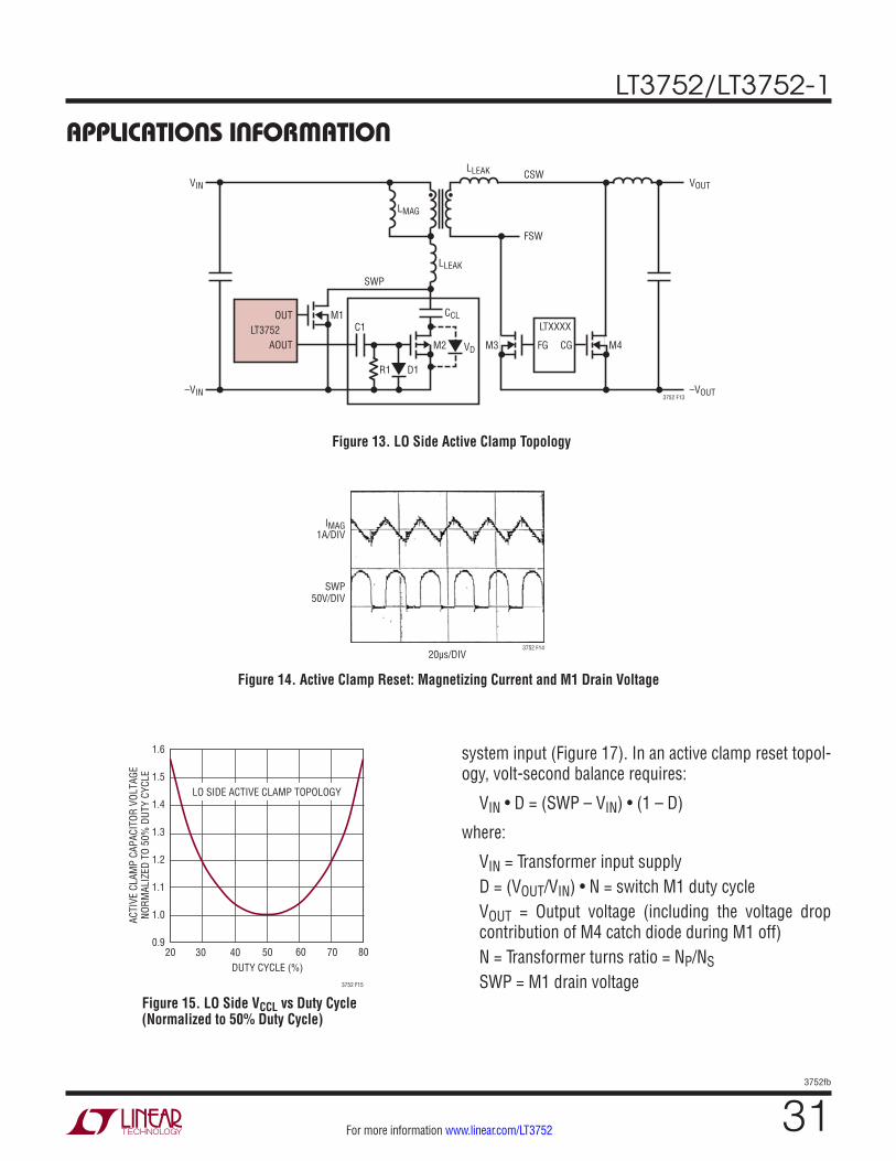
LT3752/LT3752-1
313752fb
For more information www.linear.com/LT3752
20µs/DIV
IMAG1A/DIV
SWP50V/DIV
3752 F14
APPLICATIONS INFORMATION
system input (Figure 17). In an active clamp reset topol-ogy, volt-second balance requires:
VIN • D = (SWP – VIN) • (1 – D)
where:
VIN = Transformer input supplyD = (VOUT/VIN) • N = switch M1 duty cycleVOUT = Output voltage (including the voltage drop contribution of M4 catch diode during M1 off)N = Transformer turns ratio = NP/NSSWP = M1 drain voltage
DUTY CYCLE (%)20
1.6
1.5
1.4
1.3
1.2
1.1
1.0
0.950 70
3752 F15
30 40 60 80
ACTI
VE C
LAM
P CA
PACI
TOR
VOLT
AGE
NORM
ALIZ
ED T
O 50
% D
UTY
CYCL
E
LO SIDE ACTIVE CLAMP TOPOLOGY
Figure 15. LO Side VCCL vs Duty Cycle (Normalized to 50% Duty Cycle)
Figure 14. Active Clamp Reset: Magnetizing Current and M1 Drain Voltage
Figure 13. LO Side Active Clamp Topology
CCL
LLEAK
LLEAK
LMAG
FSW
CSW
• •
VD
D1R1
C1
M2 M4M3
M1
SWP
OUT
VIN
–VIN
VOUT
–VOUT
AOUTLT3752
FG
LTXXXX
CG
3752 F13

LT3752/LT3752-1
323752fb
For more information www.linear.com/LT3752
Figure 16. HI Side VCCL vs Duty Cycle (Normalized to 50% Duty Cycle)
DUTY CYCLE (%)20
ACTI
VE C
LAM
P CA
PACI
TOR
VOLT
AGE
NORM
ALIZ
ED T
O 50
% D
UTY
CYCL
E
1.5
3752 F16
1.0
0.540 6030 50 70
2.0
2.5
1.3
0.8
1.8
2.3
80
HI SIDE ACTIVE CLAMP TOPOLOGY
Figure 17. HI Side Active Clamp Topology
APPLICATIONS INFORMATIONLO Side Active Clamp Topology (LT3752)
The steady-state active clamp capacitor voltage, VCCL, required to reset the transformer in a LO side active clamp topology (Figure 13) can be approximated as the drain-to-source voltage (VDS) of switch M1, given by:
VCCL (LO side):
(a) Steady state: VCCL = SWP = VDS
=1
1– D
• VIN =
VIN2
VIN – VOUT •N( )( ) (b) Transient:
During load transients, duty cycle and hence VCCL may increase. Replace D with DVSEC in the equation above to calculate transient VCCL values. See the previous section Programming Duty Cycle Clamp–DVSEC. The DVSEC guard-rail can be programmed as close as 5% higher than D but may require a larger margin to improve transient response.
As shown in Figure 15, the maximum steady-state value for VCCL may occur at minimum or maximum input volt-age. Hence VCCL should be calculated at both input voltage levels and the largest of the two calculations used. M1 drain should be rated for a voltage greater than the above steady-state VDS calculation due to tolerances in duty cycle, load transients, voltage ripple on CCL and leakage inductance spikes. CCL should be rated higher due to the effect of voltage coefficient on capacitance value. A typical choice for CCL is a good quality X7R capacitor. M2 should have a VDS rating greater than VCCL since the bottom plate of CCL is –VCCL during M1 on and M2 off. For high input voltage applications, the limited VDS rating of available P-channel MOSFETs might require changing from a LO side to HI side active clamp topology.
For the lo side active clamp topology in steady state, during M1 on time, magnetizing current (IMAG) increases from a negative value to a positive value (Figure 14). When M1 turns off, magnetizing current charges SWP until it reaches VCCL plus the voltage drop of the M2 body diode. At this
CCL
LLEAK
LLEAK
SWP
LMAG
FSW
CSW
• •
• •VD
D1
–VIN
C2T4
C1
M2
M4
M1
M3
R1
OUT
VIN
–VIN
VOUT
–VOUT
AOUT
LT3752-1
FG
LTXXXX
CG
3752 F17

LT3752/LT3752-1
333752fb
For more information www.linear.com/LT3752
APPLICATIONS INFORMATIONmoment the active clamp capacitor is passively switched in to ground (due to the forward conduction of M2 body diode) and the drain voltage increases at a slower rate due to the loading of CCL. SWP above VIN causes IMAG to reduce from a positive value towards zero (dVSWP/dT = 0). As IMAG becomes negative it begins to discharge the SWP node. Switching in M2 before IMAG reverses, actively connects the bottom plate of CCL to ground and allows SWP to be discharged slowly. The resulting SWP waveform during M1 off-time appears as a square wave with a superimposed sinusoidal peak representing ripple voltage on CCL.
The switch M2 experiences near zero voltage switching (ZVS) since only the body diode voltage drop appears across it at switch turn on.
HI Side Active Clamp Topology (LT3752-1)
For high input voltage applications the VDS rating of avail-able P-channel MOSFETs might not be high enough to be used as the active clamp switch in the LO side active clamp topology (Figure 13). An N-channel approach using the HI side active clamp topology (Figure 17) should be used. This topology requires a gate drive transformer or a simple gate drive opto-coupler to drive the N-channel MOSFET (M2) for switching in the active clamp capacitor from SWP to VIN. The M1 drain voltage calculation is the same as in the LO side active clamp case and M1 should be rated in a similar manner. The voltage across the clamp capacitor in the HI side architecture, however, is lower by VIN since it is referenced to VIN.
The steady-state active clamp capacitor voltage VCCL to reset the transformer in a HI side active clamp topology can be approximated by:
VCCL (HI side):
(a) Steady state: VCCL = VRESET = VDS – VIN
=
D1– D
• VIN = VIN • VOUT •
NVIN – VOUT •N( )
(b) Transient:
During load transients, duty cycle and hence VCCL may increase. Replace D with DVSEC in the equation above to calculate transient VCCL values. DVSEC guardrail can be programmed as close as 6% higher than D but may require a larger margin to improve transient response. See the previous section Programming Duty Cycle Clamp–DVSEC.
CCL should be rated for a voltage higher than the above steady-state calculation due to tolerances in duty cycle, load transients, voltage ripple on CCL and the effect of voltage coefficient on capacitance value. A typical choice for CCL is a good quality (X7R) capacitor. When using a gate drive transformer to provide control of the active clamp switch (M2), the external components C1, C2, R1, D1 and T4 are required. T4 size will increase for lower programmed switching frequencies due to a minimum volt-second requirement. Alternatively, a simple gate driver opto-coupler can be used as a switch to control M2, for a smaller solution size. The input supply capacitor for the gate drive opto-coupler is easily charged using the housekeep-ing supply of the LT3752-1. Common component values are shown in the Typical Applications section.
Active Clamp Capacitor Value and Voltage Ripple
The active clamp capacitor value should be chosen based on the amount of voltage ripple which can be tolerated by components attached to SWP. Lower CCL values will create larger voltage ripple (increased drain voltage for the primary side power MOSFET) but will require less swing in magnetizing current to move the active clamp capacitor during duty cycle changes. Choosing too high a value for the active clamp capacitor (beyond what is needed to keep ripple voltage to an acceptable level) will require unneces-sary additional flux swing during transient conditions. For systems with flux swing detection, too high a value for the active clamp capacitor will trigger the detection system early and degrade transient response.

LT3752/LT3752-1
343752fb
For more information www.linear.com/LT3752
APPLICATIONS INFORMATIONAnother factor to consider is the resonance between CCL and the magnetizing inductance (LMAG) of the main transformer. An RC snubber (RS, CS) in parallel with CCL will dampen the sinusoidal ringing and limit the peak voltages at the primary side MOSFET drain during input/load transients. Check circuit performance to determine if the snubber is required. Component values can be approximated as:
CCL (active clamp capacitance) =
10LMAG
•(1–DMIN)2• π • fOSC
2
where,
DMIN = (VOUT/VIN(MAX)) • NP/NS
and (if needed),
CS (snubber capacitance) = 6 • CCL
RS (snubber resistance) = (1/(1-DMAX)) • √(LMAG/CCL)
where,
DMAX = ( VOUT/VIN(MIN)) • NP/NS
Check the voltage ripple on SWP during steady-state operation.
CCL voltage ripple can be estimated as:
VCCL(RIPPLE) = VCCL • (1-D)2/(8 • CCL • LMAG • fOSC2)
where,
D = (VOUT/VIN) • (NP/NS)
VCCL = VIN/(1-D) (Lo side active clamp topology)
VCCL = D • VIN/(1-D) (Hi side active clamp topology)
Example : For VIN = 36V, VOUT = 12V, NP/NS = 2, VCCL = 108V (Lo side active clamp topology), CCL = 22nF, LMAG = 100µH, fOSC = 250kHz, VCCL(RIPPLE) = 108(0.33)2/(8(22 • 10–9)(10–4)(2.5 • 104)2) = 10.7V
The transformer is typically chosen to operate at a maximum flux density that is low enough to avoid excessive core losses. This also allows enough headroom during input and load transients to move the active clamp capacitor at a fast enough rate to keep up with duty cycle changes.
Active Clamp MOSFET Selection
The selection of active clamp MOSFET is determined by the maximum levels expected for the drain voltage and drain current. The active clamp switch (M2) in a either a lo side or hi side active clamp topology has the same BVdss requirements as the main N-channel power MOSFET. The current requirements are divided into two categories :
(A) Drain Current
This is typically less than the main N-channel power MOSFET because the active clamp MOSFET sees only magnetizing current, estimated as :
Peak IMAG (steady state) = (1/2) • (NP/NS) • (VOUT/ LMAG) • (1/fOSC)
where,
LMAG = main transformer’s magnetizing inductance
Example (LT3752) : For VOUT =12V, NP/NS = 2, fOSC = 250kHz and LMAG = 100µH, Peak IMAG = 0.48A.
This value should be doubled for safety margin due to variations in LMAG, fOSC and transient conditions.
(B) Body Diode Current
The body diode will see reflected output current as a pulse every time the main N-channel power MOSFET turns off. This is due to residual energy stored in the transformer's leakage inductance. The body diode of the active clamp MOSFET should be rated to withstand a forward pulsed current of:
ID(MAX) = (NS/NP) (IOUT(MAX) + (IL(RIPPLE)(P-P)/2))
where,
IL(RIPPLE)(P-P) = output inductor ripple current = (VOUT/ (LOUT • fOSC)) • (1–(VOUT/VIN)(NP/NS))
IOUT(MAX) = maximum output load current

LT3752/LT3752-1
353752fb
For more information www.linear.com/LT3752
APPLICATIONS INFORMATIONProgramming Active Clamp Switch Timing: AOUT to OUT (tAO) and OUT to AOUT (tOA) Delays
The timings tAO and tOA represent the delays between AOUT and OUT edges (Figures 1 and 2) and are programmed by a single resistor, RTAO, connected from analog ground (Pin 18) to the TAO pin. Once tAO is programmed for the reasons given below, tOA will be automatically generated.
Front-end timing tAO (M2 off, M1 on)
= AOUT(edge)-to-OUT(rising)
= 50ns + 3.8ns •
RTAO1k
, 14.7k < RTAO < 125k
In order to minimize turn-on transition loss in M1 the drain of M1 should be as low as possible before M1 turns on. To achieve this, AOUT should turn M2 off a delay of tAO before OUT turns M1 on. This allows the main transformer’s magnetizing current to discharge M1 drain voltage quickly towards VIN before M1 turns on.
As SWP falls below VIN, however, the rectifying diodes on the secondary side are typically active and clamp the SWP node close to VIN. If enough leakage inductance exists, however, the clamping action on SWP by the secondary side will be delayed—potentially allowing the drain of M1 to be fully discharged to ground just before M1 turns on. Even with this delay due to the leakage inductance, LMAG needs to be low enough to allow IMAG to be negative enough to slew SWP down to ground before M1 turns on. If achievable, M1 will experience zero voltage switching (ZVS) for highest efficiency. As will be seen in a later sec-tion entitled Primary-Side Power MOSFET Selection, M1 transition loss is a significant contributor to M1 losses.
Back-end timing tOA (M1 off, M2 on) is automatically generated
= OUT(falling)-to-AOUT(edge) = 0.9 • tAO
tOA should be checked to ensure M2 is not turned on until M1 and M3 are turned off.
Programming Synchronous Rectifier Timing: SOUT to OUT (tSO) and OUT to SOUT (tOS) Delays
The LT3752/LT3752-1 include a ±0.4A gate driver at the SOUT pin to send a control signal via a pulse transformer to the secondary side of the forward converter for syn-chronous rectification (see Figures 1 and 2). For the highest efficiency, M4 should be turned on whenever M1 is turned off. This suggests that SOUT should be a non-overlapping signal with OUT with very small non-overlap times. Inherent timing delays, however, which can vary from application to application, can exist between OUT to CSW and between SOUT to CG. Possible shoot-through can occur if both M1 and M4 are on at the same time, resulting in transformer and/or switch damage.
Front-end timing: tSO (M4 off, M1 on) = SOUT(falling)-to-OUT(rising) delay = tSO = tAO – tAS = 3.8ns • (RTAS – RTAO)
where:
tAS = 50ns + (3.8ns • RTAS/1k) , 14.7k < RTAS < 125k, tAO = 50ns + (3.8ns • RTAO/1k), 14.7k < RTAO < 125k,
tSO is defined by resistors RTAS and RTAO connected from analog ground (Pin 18) to their respective pins TAS and TAO. Each of these resistor defines a delay referenced to the AOUT edge at the start of each cycle. RTAO was already programmed based on requirements defined in the previous section Programming AOUT to OUT Delay. RTAS is then programmed as a delay from AOUT to SOUT to fulfill the equation above for tSO. By choosing RTAS less than or greater than RTAO, the delay between SOUT falling and OUT rising can be programmed as positive or nega-tive. While a positive delay can always be programmed for tSO, the ability to program a negative delay allows for improved efficiency if OUT(rising)-to-CSW(rising) delay is larger than SOUT(falling)-to-CG(rising) delay.
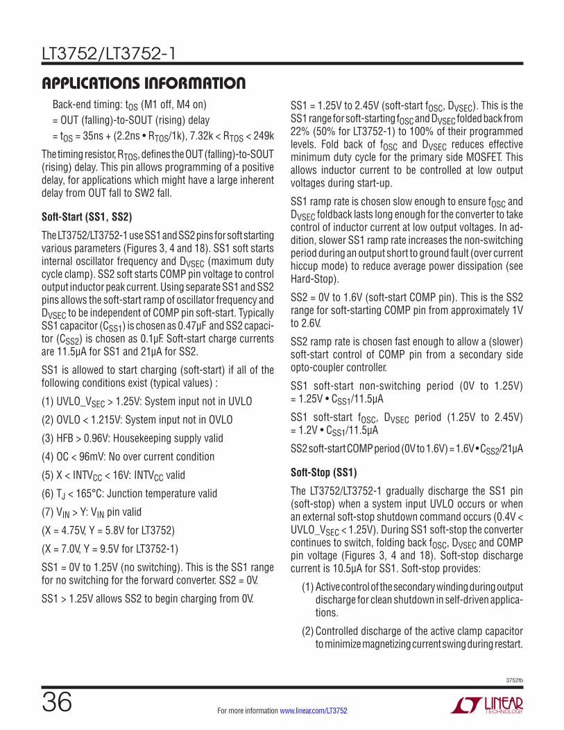
LT3752/LT3752-1
363752fb
For more information www.linear.com/LT3752
APPLICATIONS INFORMATIONBack-end timing: tOS (M1 off, M4 on)= OUT (falling)-to-SOUT (rising) delay = tOS = 35ns + (2.2ns • RTOS/1k), 7.32k < RTOS < 249k
The timing resistor, RTOS, defines the OUT (falling)-to-SOUT (rising) delay. This pin allows programming of a positive delay, for applications which might have a large inherent delay from OUT fall to SW2 fall.
Soft-Start (SS1, SS2)
The LT3752/LT3752-1 use SS1 and SS2 pins for soft starting various parameters (Figures 3, 4 and 18). SS1 soft starts internal oscillator frequency and DVSEC (maximum duty cycle clamp). SS2 soft starts COMP pin voltage to control output inductor peak current. Using separate SS1 and SS2 pins allows the soft-start ramp of oscillator frequency and DVSEC to be independent of COMP pin soft-start. Typically SS1 capacitor (CSS1) is chosen as 0.47µF and SS2 capaci-tor (CSS2) is chosen as 0.1µF. Soft-start charge currents are 11.5µA for SS1 and 21µA for SS2.
SS1 is allowed to start charging (soft-start) if all of the following conditions exist (typical values) :
(1) UVLO_VSEC > 1.25V: System input not in UVLO
(2) OVLO < 1.215V: System input not in OVLO
(3) HFB > 0.96V: Housekeeping supply valid
(4) OC < 96mV: No over current condition
(5) X < INTVCC < 16V: INTVCC valid
(6) TJ < 165°C: Junction temperature valid
(7) VIN > Y: VIN pin valid
(X = 4.75V, Y = 5.8V for LT3752)
(X = 7.0V, Y = 9.5V for LT3752-1)
SS1 = 0V to 1.25V (no switching). This is the SS1 range for no switching for the forward converter. SS2 = 0V.
SS1 > 1.25V allows SS2 to begin charging from 0V.
SS1 = 1.25V to 2.45V (soft-start fOSC, DVSEC). This is the SS1 range for soft-starting fOSC and DVSEC folded back from 22% (50% for LT3752-1) to 100% of their programmed levels. Fold back of fOSC and DVSEC reduces effective minimum duty cycle for the primary side MOSFET. This allows inductor current to be controlled at low output voltages during start-up.
SS1 ramp rate is chosen slow enough to ensure fOSC and DVSEC foldback lasts long enough for the converter to take control of inductor current at low output voltages. In ad-dition, slower SS1 ramp rate increases the non-switching period during an output short to ground fault (over current hiccup mode) to reduce average power dissipation (see Hard-Stop).
SS2 = 0V to 1.6V (soft-start COMP pin). This is the SS2 range for soft-starting COMP pin from approximately 1V to 2.6V.
SS2 ramp rate is chosen fast enough to allow a (slower) soft-start control of COMP pin from a secondary side opto-coupler controller.
SS1 soft-start non-switching period (0V to 1.25V) = 1.25V • CSS1/11.5µA
SS1 soft-start fOSC, DVSEC period (1.25V to 2.45V) = 1.2V • CSS1/11.5µA
SS2 soft-start COMP period (0V to 1.6V) = 1.6V • CSS2/21µA
Soft-Stop (SS1)
The LT3752/LT3752-1 gradually discharge the SS1 pin (soft-stop) when a system input UVLO occurs or when an external soft-stop shutdown command occurs (0.4V < UVLO_VSEC < 1.25V). During SS1 soft-stop the converter continues to switch, folding back fOSC, DVSEC and COMP pin voltage (Figures 3, 4 and 18). Soft-stop discharge current is 10.5µA for SS1. Soft-stop provides:
(1) Active control of the secondary winding during output discharge for clean shutdown in self-driven applica- tions.
(2) Controlled discharge of the active clamp capacitor to minimize magnetizing current swing during restart.

LT3752/LT3752-1
373752fb
For more information www.linear.com/LT3752
APPLICATIONS INFORMATIONSS1: 2.45V to 1.25V (soft-stop fOSC, DVSEC, COMP). This is the SS1 range for soft-stop folding back of:
(1) fOSC and DVSEC from 100% to 22% (50% for LT3752-1) of their programmed levels.
(2) COMP pin (100% to 0% of commanded peak current).
SS1 soft-stop fOSC , DVSEC, COMP period (2.45V to 1.25V) = 1.2V • CSS1/10.5µA
SS1 < 1.25V. Forward converter stops switching and SS2 pin is discharged to 0V using 2.8mA.
SS1 = 1.25V to 0V: When SS1 falls below 0.15V the internal SS1 latch is reset. If all faults are removed, SS1 begins charging again. If faults still remain, SS1 discharges to 0V.
SS1 soft-stop non-switching period (1.25V to 0V) = 1.25V • CSS1/10.5µA
DVSEC rises as system input voltage falls in order to provide a maximum duty cycle guardrail (volt-second clamp). When system input falls below it's UVLO thresh-old, however, this triggers a soft-stop with the converter continuing to switch. It is important that DVSEC no longer increases even though system input voltage may still be falling. The LT3752/LT3752-1 achieve an upper clamp on DVSEC by clamping the minimum level for the IVSEC pin to 1.25V. As SS1 pin discharges during soft-stop it folds back DVSEC. As DVSEC falls below the natural duty cycle of the converter, the converter loop follows DVSEC. If the system input voltage rises (IVSEC pin rises) during soft-stop the volt-second clamp circuit further reduces DVSEC. The I.C. chooses the lowest DVSEC commanded by either the IVSEC pin or the SS1 soft-stop function.
Hard-Stop (SS1, SS2)
Switching immediately stops and both SS1 and SS2 pins are rapidly discharged (Figure 18. Hard-Stop) if any of the following faults occur (typical values):
(1) UVLO_VSEC < 0.4V: Micropower shutdown
(2) OVLO > 1.250V: System input OVLO
(3) HFB < 0.92V: Housekeeping supply UVLO
(4) OC > 96mV: Over current condition
(5) INTVCC < X(UVLO), > 16.5V (OVLO)
(6) TJ > 170°C: Thermal shutdown
(7) VIN < Y: VIN pin UVLO
(X = 4.6V, Y = 5.5V for LT3752)
(X = 6.8V, Y = 7.6V for LT3752-1)
Switching stops immediately for any of the faults listed above. When SS1 discharges below 0.15V it begins charg-ing again if all faults have been removed. For an over cur-rent fault triggered by OC > 96mV, the disable of switching will cause the OC pin voltage to fall back below 96mV. This will allow SS1 and SS2 to recharge and eventually attempt switching again. If the over current condition still exists, OC pin will exceed 96mV again and the discharge/charge cycle of SS1 and SS2 will repeat in a hiccup mode. The non-switching dead time period during hiccup mode reduces the average power seen by the converter in an over current fault condition. The dead time is dominated by SS1 recharging from 0.15V to 1.25V.
Non-switching period in over current (hiccup mode): = 1.1V • CSS1/11.5µA
OUT, AOUT, SOUT Pulse-Skipping Mode
During load steps, initial soft-start, end of soft-stop or light load operation (if the forward converter is designed to operate in DCM), the loop may require pulse skipping on the OUT pin. This occurs when the COMP pin falls below its switching threshold. If the COMP pin falls below it's switching threshold while OUT is turned on, the LT3752/LT3752-1 will immediately turn OUT off ; both AOUT and SOUT will complete their normal signal timings referenced from the OUT falling edge. If the COMP pin remains below it's switching threshold at the start of the next switching cycle, the LT3752/LT3752-1 will skip the next OUT pulse and therefore also skip AOUT and SOUT pulses. For AOUT control, this prevents the active clamp capacitor from be-
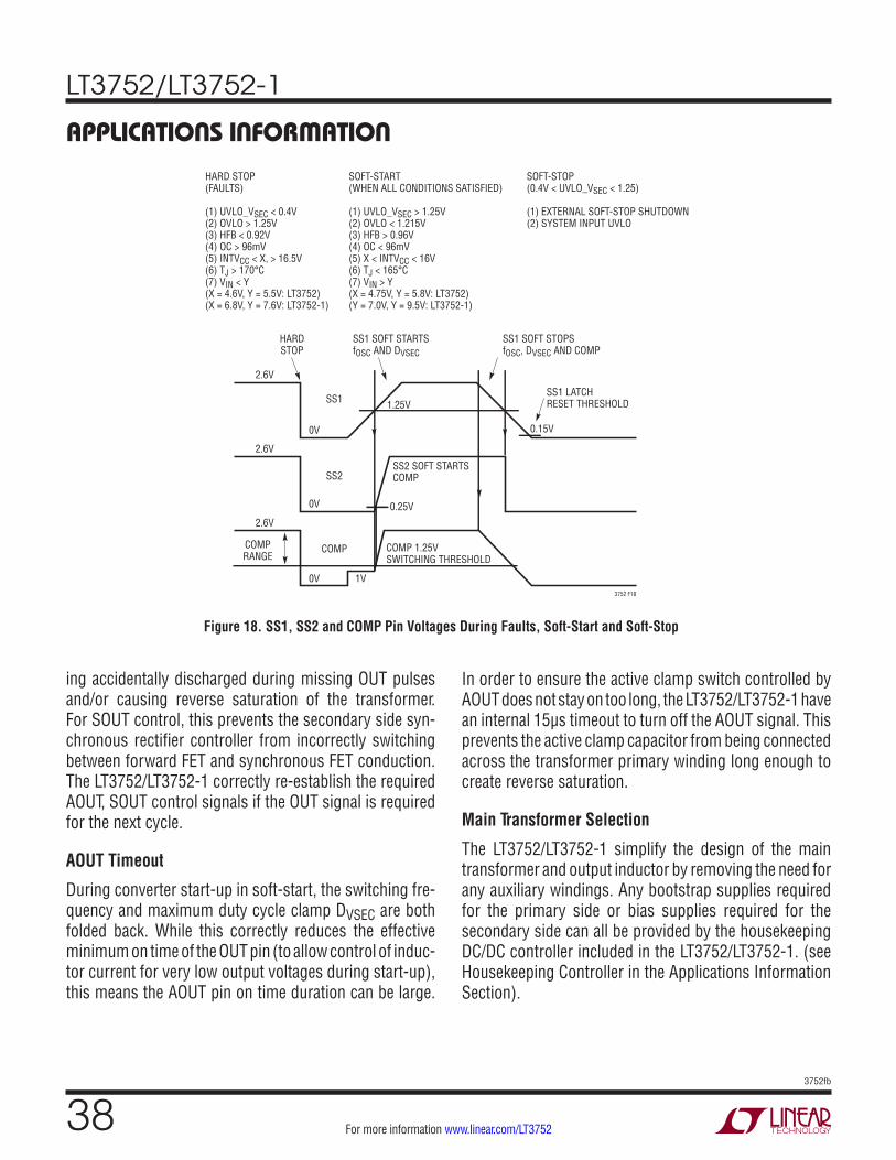
LT3752/LT3752-1
383752fb
For more information www.linear.com/LT3752
ing accidentally discharged during missing OUT pulses and/or causing reverse saturation of the transformer. For SOUT control, this prevents the secondary side syn-chronous rectifier controller from incorrectly switching between forward FET and synchronous FET conduction. The LT3752/LT3752-1 correctly re-establish the required AOUT, SOUT control signals if the OUT signal is required for the next cycle.
AOUT Timeout
During converter start-up in soft-start, the switching fre-quency and maximum duty cycle clamp DVSEC are both folded back. While this correctly reduces the effective minimum on time of the OUT pin (to allow control of induc-tor current for very low output voltages during start-up), this means the AOUT pin on time duration can be large.
In order to ensure the active clamp switch controlled by AOUT does not stay on too long, the LT3752/LT3752-1 have an internal 15µs timeout to turn off the AOUT signal. This prevents the active clamp capacitor from being connected across the transformer primary winding long enough to create reverse saturation.
Main Transformer Selection
The LT3752/LT3752-1 simplify the design of the main transformer and output inductor by removing the need for any auxiliary windings. Any bootstrap supplies required for the primary side or bias supplies required for the secondary side can all be provided by the housekeeping DC/DC controller included in the LT3752/LT3752-1. (see Housekeeping Controller in the Applications Information Section).
APPLICATIONS INFORMATION
Figure 18. SS1, SS2 and COMP Pin Voltages During Faults, Soft-Start and Soft-Stop
COMPRANGE
2.6V
2.6V
0V
0V
1.25V
0.15V
0.25V
COMP 1.25VSWITCHING THRESHOLD
SS2 SOFT STARTSCOMP
0V 1V
COMP
SS2
SS1
2.6V
HARDSTOP
SOFT-START(WHEN ALL CONDITIONS SATISFIED)
(1) UVLO_VSEC > 1.25V(2) OVLO < 1.215V(3) HFB > 0.96V(4) OC < 96mV(5) X < INTVCC < 16V(6) TJ < 165°C(7) VIN > Y(X = 4.75V, Y = 5.8V: LT3752)(Y = 7.0V, Y = 9.5V: LT3752-1)
SOFT-STOP(0.4V < UVLO_VSEC < 1.25)
(1) EXTERNAL SOFT-STOP SHUTDOWN(2) SYSTEM INPUT UVLO
HARD STOP(FAULTS)
(1) UVLO_VSEC < 0.4V(2) OVLO > 1.25V(3) HFB < 0.92V(4) OC > 96mV(5) INTVCC < X, > 16.5V(6) TJ > 170°C(7) VIN < Y(X = 4.6V, Y = 5.5V: LT3752)(X = 6.8V, Y = 7.6V: LT3752-1)
3752 F18
SS1 SOFT STOPSfOSC, DVSEC AND COMP
SS1 SOFT STARTSfOSC AND DVSEC
SS1 LATCHRESET THRESHOLD

LT3752/LT3752-1
393752fb
For more information www.linear.com/LT3752
The selection of the main transformer will depend on the applications requirements : isolation voltage, power level, maximum volt-seconds, turns ratio, component size, power losses and switching frequency.
Transformer construction using the planar winding technol-ogy is typically chosen for minimizing leakage inductance and reducing component height. Transformer core type is usually a ferrite material for high frequency applications.
Find a family of transformers that meet both the isolation and power level requirements of the application. The next step is to find a transformer within that family which is suitable for the application. The subsequent thought pro-cess for the transformer design will include :
(1) Secondary turns (NS), core losses, temperature rise, flux density, switching frequency
(2) Primary turns (NP), maximum duty cycle and reset voltages
(3) Copper losses
The expression for secondary turns (NS) is given by,
NS = 108 VOUT/(fOSC • AC • BM)
where,
AC = cross-sectional area of the core in cm2
BM = maximum AC flux density desired
For flux density, choose a level which achieves an accept-able level of core loss/temperature rise at a given switching frequency. The transformer data sheet will provide curves of core loss versus flux density at various switching fre-quencies. The data sheet will also provide temperature rise versus core loss. While choosing a value for BM to avoid excessive core losses will usually allow enough headroom for flux swing during input / load transients, still make sure to stay well below the saturation flux density of the transformer core. If needed, increasing NS will reduce flux
density. After calculating NS, the number of primary turns (NP) can be calculated from,
NP = NS • DMAX VIN(MIN)/VOUT
where,
VIN(MIN) = minimum system input voltage
DMAX = maximum switch duty cycle at VIN(MIN) (typically chosen between 0.6 and 0.7)
At minimum input voltage the converter will run at a maxi-mum duty cycle DMAX. A higher transformer turns ratio (NP/NS) will create a higher DMAX but it will also require higher voltages at the drain of the primary side switch to reset the transformer (see previous sections Lo side Active Clamp Topology and Hi side Active Clamp Topology). DMAX values are typically chosen between 0.6 and 0.7. Even for a given DMAX value, the loop must also provide protection against duty cycles that may excessively exceed DMAX during transients or faults. While most converters only provide a fixed duty cycle clamp, the LT3752/LT3752-1 provide a programmable maximum duty cycle clamp DVSEC that also moves inversely with input voltage.
The resulting function is that of a programmable volt-second clamp. This allows the user to choose a transformer turns ratio for DMAX and then customize a maximum duty cycle clamp DVSEC above DMAX for safety. DVSEC then follows the natural duty cycle of the converter as a safety guardrail (see previous section Programming Duty Cycle Clamp).
After deciding on the particular transformer and turns ratio, the copper losses can then be approximated by,
PCU = D • I(Load)(MAX)2 (RSEC + (NS/NP)2 RPRI)
where,
D = switch duty cycle (choose nominal 0.5)
I(Load)(MAX) = maximum load current
APPLICATIONS INFORMATION
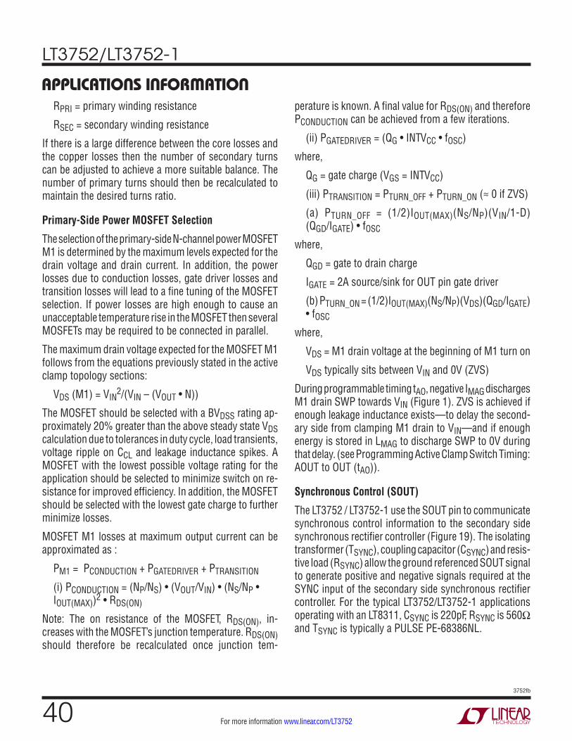
LT3752/LT3752-1
403752fb
For more information www.linear.com/LT3752
RPRI = primary winding resistance
RSEC = secondary winding resistance
If there is a large difference between the core losses and the copper losses then the number of secondary turns can be adjusted to achieve a more suitable balance. The number of primary turns should then be recalculated to maintain the desired turns ratio.
Primary-Side Power MOSFET Selection
The selection of the primary-side N-channel power MOSFET M1 is determined by the maximum levels expected for the drain voltage and drain current. In addition, the power losses due to conduction losses, gate driver losses and transition losses will lead to a fine tuning of the MOSFET selection. If power losses are high enough to cause an unacceptable temperature rise in the MOSFET then several MOSFETs may be required to be connected in parallel.
The maximum drain voltage expected for the MOSFET M1 follows from the equations previously stated in the active clamp topology sections:
VDS (M1) = VIN2/(VIN – (VOUT • N))
The MOSFET should be selected with a BVDSS rating ap-proximately 20% greater than the above steady state VDS calculation due to tolerances in duty cycle, load transients, voltage ripple on CCL and leakage inductance spikes. A MOSFET with the lowest possible voltage rating for the application should be selected to minimize switch on re-sistance for improved efficiency. In addition, the MOSFET should be selected with the lowest gate charge to further minimize losses.
MOSFET M1 losses at maximum output current can be approximated as :
PM1 = PCONDUCTION + PGATEDRIVER + PTRANSITION
(i) PCONDUCTION = (NP/NS) • (VOUT/VIN) • (NS/NP • IOUT(MAX))2 • RDS(ON)
Note: The on resistance of the MOSFET, RDS(ON), in-creases with the MOSFET’s junction temperature. RDS(ON) should therefore be recalculated once junction tem-
perature is known. A final value for RDS(ON) and therefore PCONDUCTION can be achieved from a few iterations.
(ii) PGATEDRIVER = (QG • INTVCC • fOSC)
where,
QG = gate charge (VGS = INTVCC)
(iii) PTRANSITION = PTURN_OFF + PTURN_ON (≈ 0 if ZVS)
(a) PTURN_OFF = (1/2)IOUT(MAX)(NS/NP)(VIN/1-D) (QGD/IGATE) • fOSC
where,
QGD = gate to drain charge
IGATE = 2A source/sink for OUT pin gate driver
(b) PTURN_ON = (1/2)IOUT(MAX)(NS/NP)(VDS)(QGD/IGATE) • fOSC
where,
VDS = M1 drain voltage at the beginning of M1 turn on
VDS typically sits between VIN and 0V (ZVS)
During programmable timing tAO, negative IMAG discharges M1 drain SWP towards VIN (Figure 1). ZVS is achieved if enough leakage inductance exists—to delay the second-ary side from clamping M1 drain to VIN—and if enough energy is stored in LMAG to discharge SWP to 0V during that delay. (see Programming Active Clamp Switch Timing: AOUT to OUT (tAO)).
Synchronous Control (SOUT)
The LT3752 / LT3752-1 use the SOUT pin to communicate synchronous control information to the secondary side synchronous rectifier controller (Figure 19). The isolating transformer (TSYNC), coupling capacitor (CSYNC) and resis-tive load (RSYNC) allow the ground referenced SOUT signal to generate positive and negative signals required at the SYNC input of the secondary side synchronous rectifier controller. For the typical LT3752/LT3752-1 applications operating with an LT8311, CSYNC is 220pF, RSYNC is 560Ω and TSYNC is typically a PULSE PE-68386NL.
APPLICATIONS INFORMATION

LT3752/LT3752-1
413752fb
For more information www.linear.com/LT3752
Typically choose CSYNC between 220pF and 1nF. RSYNC should then be chosen to obey :
(1) SOUTMAX/100mA ≤ RSYNC ≤ √(LMAG/CSYNC)
where,
SOUTMAX = INTVCC
LMAG = TSYNC’S magnetizing inductance
100mA = SOUT gate driver minimum source current
and
(2) RSYNC • CSYNC ≥ (–1) • Y/(ln (Z/SOUTMAX))
where,
Y = SYNC minimum pulse duration (50ns; LT8311)
Z = |SYNC level to achieve Y| (±2V: LT8311)
Even though the LT3752/LT3752-1 INTVCC pin is allowed to be over driven by as much as 15.4V using the house-keeping supply, SOUTMAX level should be designed to not cause TSYNC output to exceed the maximum ratings of the LT8311’s SYNC pin.
Cost/Space reduction : If discontinuous conduction mode (DCM) operation is acceptable at light load, the LT8311 has a preactive mode which controls the synchronous MOSFETs without TSYNC, CSYNC, RSYNC or the LT3752/LT3752-1 timing resistors RTAS, RTOS (leave open).
Output Inductor Value
The choice of output inductor value LOUT will depend on the amount of allowable ripple current. The inductor ripple current is given by:
IL(RIPPLE)(P-P)
= ∆IL = (VOUT/(LOUT • fOSC)) • (1 – (VOUT/VIN)(NP/NS))
The LT3752/LT3752-1 allow very large ∆IL values (low LOUT values) without the worry of insufficient slope compensa-tion—by allowing slope compensation to be programmed with an external resistor in series with the ISENSEP pin (see Current Sensing and Programmable Slope Compensation).
Larger ∆IL will allow lower LOUT, reducing component size, but will also cause higher output voltage ripple and core losses. For LT3752/LT3752-1 applications, ∆IL is typically chosen to be 40% of IOUT(MAX).
Output Capacitor Selection
The choice of output capacitor value is dependent on output voltage ripple requirements given by :
∆VOUT ≈ ∆IL(ESR + (1/(8 • fOSC • COUT))
where,
∆IL = output inductor ripple current IL(RIPPLE)(P-P)
ESR = effective series resistance (of COUT)
fOSC = switching frequency
COUT = output capacitance
This gives:
COUT = ∆IL/(8 • fOSC • ( ∆VOUT – ∆IL • ESR))
Typically COUT is made up of a low ESR ceramic capacitor(s) to minimize ∆VOUT. Additional bulk capacitance is added in the form of electrolytic capacitors to minimize output voltage excursions during load steps.
Input Capacitor Selection
The active clamp forward converter demands pulses of current from the input due to primary winding current and magnetizing current. The input capacitor is required to provide high frequency filtering to achieve an input voltage as close as possible to a pure DC source with low ripple voltage. For low impedance input sources and medium to low voltage input levels, a simple ceramic capacitor with low ESR should suffice. It should be rated to operate at a worst case RMS input current of :
ICIN(RMS) = (NS/NP) IOUT(MAX)/2
Figure 19. SOUT Pulse Transformer
3752 F19
CSYNC220pF
RSYNC560Ω
SYNC(SECONDARY SIDECONTROLLER)
TSYNCSOUT
(LT3752/LT3752-1) 2
1
3
5
6
4
••
••
APPLICATIONS INFORMATION

LT3752/LT3752-1
423752fb
For more information www.linear.com/LT3752
A small 1µF bypass capacitor should also be placed close to the IC between VIN and GND.
As input voltage levels increase, any use of bulk capacitance to minimize input ripple can impact on solution size and cost. In addition, inputs with higher source impedance will cause an increase in voltage ripple. In these applications it is recommended to include an LC input filter. The output impedance of the input filter should remain below the negative input impedance of the DC/DC forward converter.
PCB Layout / Thermal Guidelines
For proper operation, PCB layout must be given special attention. Critical programming signals must be able to co-exist with high dv/dt signals. Compact layout can be achieved but not at the cost of poor thermal management. The following guidelines should be followed to approach optimal performance.
1. Ensure that a local bypass capacitor is used (and placed as close as possible) between VIN and GND for the controller IC(s).
2. The critical programming resistors for timing (pins TAO,TAS,TOS,TBLNK, IVSEC and RT) must use short traces to each pin. Each resistor should also use a short trace to connect to a single ground bus specifically connected to pin 18 of the IC (GND).
3. The current sense resistor for the forward converter must use short Kelvin connections to the ISENSEP and ISENSEN pins. The current sense resistor for the housekeeping supply should have it’s ground connection as close as possible to the power ground (PGND) pin 38.
4. High dv/dt lines should be kept away from all timing resistors, current sense inputs, HCOMP/COMP pins, UVLO_VSEC/OVLO pins and both HFB and FB feedback traces.
5. Gate driver traces (HOUT, AOUT, SOUT, OUT) should be kept as short as possible.
6. When working with high power components, multiple parallel components are the best method for spread-ing out power dissipation and minimizing temperature rise. In particular, multiple copper layers connected by vias should be used to sink heat away from each power MOSFET.
7. Keep high switching current PGND paths away from signal ground. Also minimize trace lengths for those high current switching paths to minimize parasitic inductance.
APPLICATIONS INFORMATION

LT3752/LT3752-1
433752fb
For more information www.linear.com/LT3752
Figure 20. 18V to 72V, 12V/12.5A, 150W Active Clamp Isolated Forward Converter
Efficiency vs Load Current
APPLICATIONS INFORMATION
R449.9k
R522.6k
R31.82k
R67.32k
R734k
R871.5k
R931.6k
R23100k
R24100k
R102.8k
R1110k
T1: CHAMPS G45AH2-0404-04T2: BH ELECTRONICS L00-3250T3: PULSE PE-68386NLL1: CHAMPS PQI2050-6R8D1, D2, D3: BAS516D4: CENTRAL SEMI CMMR1U-02
R13560Ω
R283.16k
R27100k
VAUX
VAUX
SYNC
VIN
GND
FBLT8311PGOOD
R142k
R150.006Ω
R1610k
R180.15Ω
R17499Ω
C102.2µF
C92.2µF
INTVCC VAUX
M5ZVN4525E6
Si2325DS
D3
T2
D2
D1
M1BSC077N12NS3
M2 M3
FDMS86101BSC077N12NS3
R25100Ω
R121.1k
R261k 2.2nF
C20.33µF
C322nF
PS2801-1
C422nF
C54.7µF
C112.2µF
C1322µF16V×2
C242.2nF250V
VOUT12V12.5A
C14470µF
16V
C124.7µF
C17220nF
3752 F20a
C1868pF C19
4.7nF
C6 220pF
T3
C161µF
T AO
T AS
T OS
T BLN
KIV
SEC
RT SS1
SS2
HCOM
P
FB COM
P
OPTO
INTV
CC
TIM
ER
SS COM
PCS
P
PMOD
E
INTVCCINTVCC
SOUT
ISENSEN
ISENSEP
OUTVIN AOUTHISENSEHOUT
OC
R25.9k
R1100k
UVLO_VSEC
LT3752
SYNC
C7100nF
C815nF
T14:4
M4
R20499k
R2913.7k
L16.8µH
R30100k
R3111.3k
CSNFG
FSW CG
CSW
R21100Ω
R22100Ω
R3820k
+
••
•••
•
•C1
4.7µF100V
×3
VIN18V TO 72V
GND
OVLO
HFB
D4
C2868pF
LOAD CURRENT (A)0
EFFI
CIEN
CY (%
)
96
94
92
90
88
8663
3752 F20b
15129
24VIN48VIN72VIN
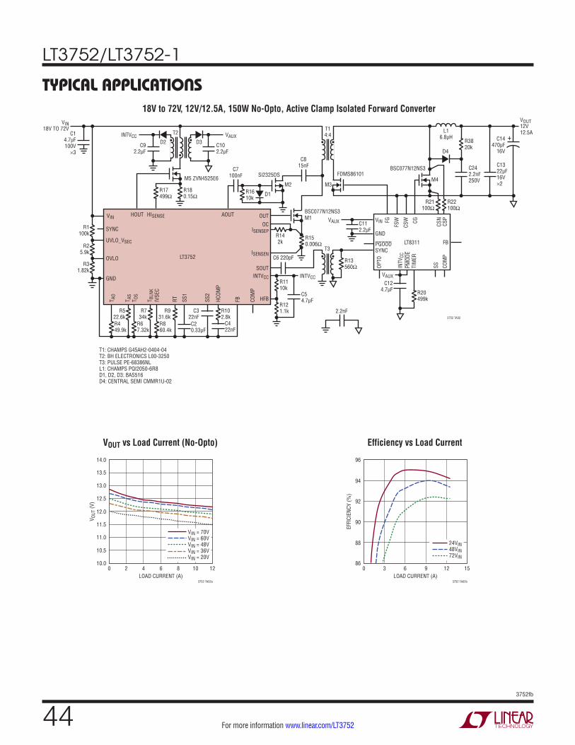
LT3752/LT3752-1
443752fb
For more information www.linear.com/LT3752
TYPICAL APPLICATIONS18V to 72V, 12V/12.5A, 150W No-Opto, Active Clamp Isolated Forward Converter
VOUT vs Load Current (No-Opto) Efficiency vs Load Current
R449.9k
R522.6k
R31.82k
R67.32k
R734k
R860.4k
R931.6k
R102.8k
R1110k
T1: CHAMPS G45AH2-0404-04T2: BH ELECTRONICS L00-3250T3: PULSE PE-68386NLL1: CHAMPS PQI2050-6R8D1, D2, D3: BAS516D4: CENTRAL SEMI CMMR1U-02
R13560Ω
VAUX
VAUX
SYNC
VIN
GND
FBLT8311PGOOD
R142k
R150.006Ω
R1610k
R180.15Ω
R17499Ω
C102.2µF
C92.2µF
INTVCC VAUX
M5 ZVN4525E6
D3
T2
D2
D1
M1BSC077N12NS3
FDMS86101
R121.1k 2.2nF
C20.33µF
C322nF
C422nF
C54.7µF
C112.2µF
C1322µF16V×2
VOUT12V12.5A
C14470µF
16V
C124.7µF
3752 TA02
C6 220pF
T3
T AO
T AS
T OS
T BLN
KIV
SEC
RT SS1
SS2
HCOM
P
FB COM
P
OPTO
INTV
CC
TIM
ER
SS COM
PCS
P
PMOD
E
INTVCC INTVCC
SOUT
ISENSEN
ISENSEP
OUTVIN AOUTHISENSEHOUT
OC
R25.9k
R1100k
UVLO_VSEC
LT3752
SYNC
C7100nF
C815nF
T14:4
R20499k
L16.8µH
CSNFG
FSW CG
CSW
R21100Ω
R22100Ω
+
••
•••
•
•C1
4.7µF100V
×3
VIN18V TO 72V
GND
OVLO
HFB
Si2325DS
M3M4
BSC077N12NS3
M2
C242.2nF250V
R3820k
D4
LOAD CURRENT (A)0
V OUT
(V)
14.0
13.5
13.0
12.5
12.0
11.0
10.5
11.5
10.042
3752 TA02a
128 106
VIN = 70VVIN = 60VVIN = 48VVIN = 36VVIN = 20V
LOAD CURRENT (A)0
EFFI
CIEN
CY (%
)
96
94
92
90
88
8663
3752 TA02b
15129
24VIN48VIN72VIN

LT3752/LT3752-1
453752fb
For more information www.linear.com/LT3752
TYPICAL APPLICATIONS150V to 400V, 12V/16.7A, 200W Active Clamp Isolated Forward Converter
Efficiency vs Load Current
R495.3k
R540.2k
R32.94k
R613k
R7100k
R8124k
R978.7k
R2322k
R2422k
R1022k
R1110k
T1: CHAMPS LT80R2-12AC-3124005T2: WÜRTH 750817020T3: PULSE PE-68386NLL1: COILCRAFT AGP2923-153D1: CENTRAL SEMI CMR1U-10D2, D3, D5: BAS516D4: CENTRAL SEMI CMMR1U-02
R13560Ω
R283.16k
R27100k
VAUX
SYNC
VIN
GNDFBLT8311PGOOD
R142k
R150.022Ω
R180.15Ω
R17499Ω
R35374k
R36374k
C104.7µFC9
10µF
INTVCC VAUXINTVCC
M5BSP300
D3
T2
D2
M1IPD65R25OC6
IPD60R1K4C6
M3
M2
R25100Ω
R12806Ω
R261.2k 2.2nF
C20.47µF
C30.22µF
PS2801-1
C43.3nF
C54.7µF
C112.2µF
C1333µF16V×4
C2410nF250V
VOUT12V16.7A
C14330µF
16V
C124.7µF
C171µF
3752 TA03
C18100pF
C1922nF
C6 220pF
T3
C161µF
T AO
T AS
T OS
T BLN
KIV
SEC
RT SS1
SS2
HCOM
P
FB COM
P
OPTO
INTV
CC
VAUX
TIM
ER
SS COM
PCS
P
PMOD
E
INTVCCINTVCC
SOUT
ISENSEN
ISENSEP
OUTVIN AOUTHISENSEHOUT
OC
R25.76k
R1499k
R34499k
UVLO_VSEC
LT3752-1
SYNC
RJK0653DPB×2
T131:5
C2010µF
D5 M4
FDMS86200×3
R20432k
R295.11k
L115µH
R30100k
R3111.3k
CSNFG
FSW CG
CSW
R21100Ω
D4
R22100Ω
R3810k
R380.002
C27120pF
+
••
•••
•
•
D1
R16 4.2ΩC12.2µF630V
VIN150V TO
400V
GND
OVLO
HFB
CATHODEANODE
ACPL-W346
VEE
VOUT
VCC
C210.22µF
C847nF630V
C1510nF630V
R19402Ω
C2868pF
LOAD CURRENT (A)0
EFFI
CIEN
CY (%
)
96
95
94
93
92
90
89
91
88
85
87
86
52.5
3752 TA03a
17.510 12.5 157.5
VIN = 150VVIN = 250VVIN = 350VVIN = 400V

LT3752/LT3752-1
463752fb
For more information www.linear.com/LT3752
TYPICAL APPLICATIONS150V to 400V, 12V/16.7A, 200W No-Opto, Active Clamp Isolated Forward Converter
VOUT vs Load Current (No-Opto) Efficiency vs Load Current
R495.3k
R540.2k
R32.94k
R613k
R7100k
R8107k
R978.7k
R1022k
R1110k
T1: CHAMPS LT80R2-12AC-3124005T2: WÜRTH 750817020T3: PULSE PE-68386NLL1: COILCRAFT AGP2923-153D1: CENTRAL SEMI CMR1U-10D2, D3, D5: BAS516D4: CENTRAL SEMI CMMR1U-02
R13560Ω
VAUX
SYNC
VIN
GND
FBLT8311PGOOD
R142k
R150.022Ω
R180.15Ω
R17499Ω
R35374k
R36374k
C104.7µFC9
10µF
INTVCC VAUXINTVCC
M5BSP300
D3
T2
D2
M1IPD65R25OC6
IPD60R1K4C6
M3
M2
R12806Ω
2.2nF
C20.47µF
C30.22µF
C43.3nF
C54.7µF
C112.2µF
C1333µF16V×4
VOUT12V16.7A
C14330µF
16V
C124.7µF
VAUX
3752 TA04
C6 220pF
T3
T AO
T AS
T OS
T BLN
KIV
SEC
RT SS1
SS2
HCOM
P
FB COM
P
OPTO
INTV
CC
TIM
ER
SS COM
P
CSP
PMOD
E
INTVCC INTVCC
SOUT
ISENSEN
ISENSEP
OUTVIN AOUTHISENSEHOUT
OC
R25.76k
R1499k
R34499k
UVLO_VSEC
LT3752-1
SYNC
RJK0653DPB×2
T131:5
C2010µF
D5M4
FDMS86200×3
R20432k
L115µH
CSNFG
FSW CG
CSW
+
••
•••
•
•
D1
ACPL-W346
R16 4.2ΩC12.2µF630V
VIN150V TO
400V
GND
OVLO
HFB
CATHODEANODE
VEE
VOUT
VCC
C210.22µF
C847nF630V
C1510nF630V
R19402Ω
R380.002
R21100Ω
R22100Ω
C27120pF
C2410nF250V
D4R3810k
LOAD CURRENT (A)0
V OUT
(V)
14.0
13.5
13.0
12.5
12.0
11.5
10.0
11.0
10.5
42
3752 TA04a
188 1210 14 166
VIN = 150VVIN = 250VVIN = 350VVIN = 400V
LOAD CURRENT (A)0
EFFI
CIEN
CY (%
)
96
95
94
93
92
90
89
91
88
85
87
86
52.5
3752 TA04b
17.510 12.5 157.5
VIN = 150VVIN = 250VVIN = 350VVIN = 400V
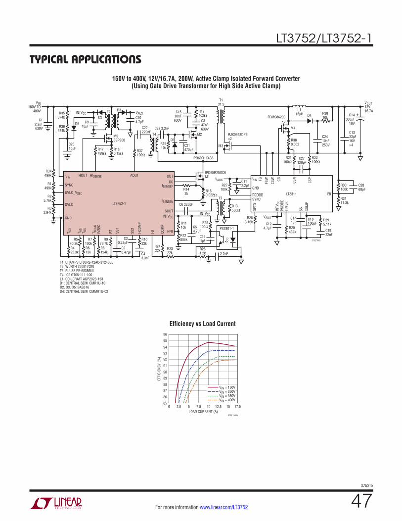
LT3752/LT3752-1
473752fb
For more information www.linear.com/LT3752
TYPICAL APPLICATIONS150V to 400V, 12V/16.7A, 200W, Active Clamp Isolated Forward Converter
(Using Gate Drive Transformer for High Side Active Clamp)
Efficiency vs Load Current
R495.3k
R540.2k
R32.94k
R613k
R7100k
R8124k
R978.7k
R2322k
R2422k
R1022k
R1110k
T1: CHAMPS LT80R2-12AC-3124005T2: WÜRTH 750817020T3: PULSE PE-68386NLT4: ICE GT05-111-100L1: COILCRAFT AGP2923-153D1: CENTRAL SEMI CMR1U-10D2, D3, D5: BAS516D4: CENTRAL SEMI CMMR1U-02
R13560Ω
R283.16k
R27100k
VAUX
SYNC
VIN
GND
FBLT8311PGOOD
R142k
R150.022Ω
R180.15Ω
R1610k
C23 3.3nF
R17499Ω
R35374k
C22220nF
R37100Ω
R36374k
C104.7µFC9
10µF
INTVCC VAUX
D1C21470pF
M5BSP300
D3T2
T4
D2
M1IPD65R25OC6
IPD60R1K4C6
M3
M2
R25100Ω
R12806k
R261.2k 2.2nF
C20.47µF
C30.22µF
PS2801-1
C43.3nF
C54.7µF
C112.2µF
C1333µF16V×4
VOUT12V16.7A
C14330µF
16V
C124.7µF
VAUX C171µF
3752 TA05
C18100pF
C1922nF
C6 220pF
T3
C161µF
T AO
T AS
T OS
T BLN
KIV
SEC
RT SS1
SS2
HCOM
P
FB COM
P
OPTO
INTV
CC
TIM
ER
SS COM
PCS
P
PMOD
E
INTVCCINTVCC
SOUT
ISENSEN
ISENSEP
OUTVIN AOUTHISENSEHOUT
OC
R25.76k
R1499k
R34499k
UVLO_VSEC
LT3752-1
SYNC
RJK0653DPB×2
T131:5
C2010µF
D5M4
FDMS86200×3
R20432k
R295.11k
L115µH
R30100k
R3111.3k
CSNFG
FSW CG
CSW
+
••
•••
•
•C1
2.2µF630V
VIN150V TO
400V
GND
OVLO
HFB
C847nF630V
C1510nF630V
R19402Ω
••
R21100Ω
R22100Ω
R380.002
C27120pF
C2410nF250V
D4 R3810k
C2868pF
LOAD CURRENT (A)0
EFFI
CIEN
CY (%
)
96
95
94
93
92
90
89
91
88
85
87
86
52.5
3752 TA05a
17.510 12.5 157.5
VIN = 150VVIN = 250VVIN = 350VVIN = 400V

LT3752/LT3752-1
483752fb
For more information www.linear.com/LT3752
TYPICAL APPLICATIONS150V to 400V, 12V/16.7A 200W, No-Opto, Active Clamp Isolated Forward Converter
(Using Gate Drive Transformer for High Side Active Clamp)
VOUT vs Load Current (No-Opto) Efficiency vs Load Current
R495.3k
R540.2k
R32.94k
R613k
R7100k
R8107k
R978.7k
R1022k
R1110k
T1: CHAMPS LT80R2-12AC-3124005T2: WÜRTH 750817020T3: PULSE PE-68386NLT4: ICE GT05-111-100L1: COILCRAFT AGP2923-153D1: CENTRAL SEMI CMR1U-10D2, D3, D5: BAS516D4: CENTRAL SEMI CMMR1U-02
R13560Ω
VAUX
SYNC
VIN
GND
FBLT8311PGOOD
R142k
R150.022Ω
R180.15Ω
R1610k
C23 3.3nF
R17499Ω
R35374k
C22220nF
R37100Ω
R36374k
C104.7µFC9
10µF
INTVCC VAUX
D1C21470pF
M5BSP300
D3T2
T4
D2
M1IPD65R25OC6
IPD60R1K4C6
M3
M2
R12806Ω
2.2nF
C20.47µF
C30.22µF
C43.3nF
C54.7µF
C112.2µF
C1333µF16V×4
VOUT12V16.7A
C14330µF
16V
C124.7µF
3752 TA06
C6 220pF
T3
T AO
T AS
T OS
T BLN
KIV
SEC
RT SS1
SS2
HCOM
P
FB COM
P
OPTO
INTV
CC
VAUX
TIM
ER
SS COM
P
CSP
PMOD
E
INTVCC
SOUT
ISENSEN
ISENSEP
OUTVIN AOUTHISENSEHOUT
OC
R25.76k
R1499k
R34499k
UVLO_VSEC
LT3752-1
SYNC
RJK0653DPB×2
T131:5
C2010µF
D5M4
FDMS86200×3
R20432k
L115µH
CSNFG
FSW CG
CSW
+
••
•••
•
•C1
2.2µF630V
VIN150V TO
400V
GND
OVLO
HFB
C847nF630V
C1510nF630V
R19402Ω
••
R21100Ω
R380.002Ω
R22100Ω
C27120pF
C2410nF250V
D4 R3810k
LOAD CURRENT (A)0
V OUT
(V)
14.0
13.5
13.0
12.5
12.0
11.5
10.0
11.0
10.5
42
3752 TA06a
188 1210 14 166
VIN = 150VVIN = 250VVIN = 350VVIN = 400V
LOAD CURRENT (A)0
EFFI
CIEN
CY (%
)
96
95
94
93
92
90
89
91
88
85
87
86
52.5
3752 TA06b
17.510 12.5 157.5
VIN = 150VVIN = 250VVIN = 350VVIN = 400V

LT3752/LT3752-1
493752fb
For more information www.linear.com/LT3752
TYPICAL APPLICATIONS75V to 150V, 24V/14A 340W Active Clamp Isolated Forward Converter
(Using Gate Drive Transformer for High Side Active Clamp)
Efficiency vs Load Current
R493.1k
R553k
R35.76k
R610k
R780.1k
R882.5k
R952.3k
R2322k
R2422k
R1022k
R1110k
T1: CHAMPS LT80R2-12AC-1006T2: WÜRTH 750817020T3: PULSE PE-68386NLT4: ICE GT05-111-100L1: COILCRAFT AGP2923-153D1: CENTRAL SEMI CMR1U-10D2, D3, D5: BAS516D4: CENTRAL SEMI CMMR1U-02
R13560Ω
R283.16k
R27100k
VAUX
SYNC
VIN
GND
FBLT8311PGOOD
R142k
R150.0075Ω
R180.15Ω
R1610k
C23 3.3nF
R17499Ω
R35102k
C22220nF
R37100Ω
R36102k
C104.7µFC9
10µF
INTVCC VAUX
D1C21470pF
M5BSP300
D3T2
T4
D2
M1IPB200N25N3
IRFL214
M3
M2
R25100Ω
R12806Ω
R261.2k 2.2nF
C20.47µF
C30.22µF
PS2801-1
C43.3nF
C54.7µF
C112.2µF
C1322µF25V×4
VOUT24V14A
C14470µF
25V
C124.7µF
C170.33µF
VAUX
3752 TA07
C18100pF
C1922nF
C6 220pF
T3
C161µF
T AO
T AS
T OS
T BLN
KIV
SEC
RT SS1
SS2
HCOM
P
FB COM
P
OPTO
INTV
CC
TIM
ER
SS COM
PCS
P
PMOD
E
INTVCCINTVCC
SOUT
ISENSEN
ISENSEP
OUTVIN AOUTHISENSEHOUT
OC
R26.04k
R16.98k
R34698k
UVLO_VSEC
LT3752-1
SYNC
BSC047N08NS3×2
T110:6
C2010µF
D5M4
IPB072N15N3G
R20365k
R295.11k
L115µH
R30100k
R315.36k
CSNFG
FSW CG
CSW
+
••
•••
•
•C1
2.2µF250V
VIN75V TO
150V
GND
OVLO
HFB
C815nF250V
C154.7nF250V
R191k
••
R21100Ω
R22100Ω
R380.003Ω
C27120pF
C2410nF250V
D4 R3810k
C2868pF
LOAD CURRENT (A)0
EFFI
CIEN
CY (%
)
96
95
94
93
92
91
86
90
89
88
87
2.5
3752 TA07a
157.5 10 12.55
VIN = 75VVIN = 100VVIN = 125VVIN = 150V

LT3752/LT3752-1
503752fb
For more information www.linear.com/LT3752
PACKAGE DESCRIPTIONPlease refer to http://www.linear.com/designtools/packaging/ for the most recent package drawings.
4.75(.187)
REF
FE38 (AB) TSSOP REV B 0910
0.09 – 0.20(.0035 – .0079)
0° – 8°
0.25REF
0.50 – 0.75(.020 – .030)
4.30 – 4.50*(.169 – .177)
1 19PIN NUMBERS 23, 25, 27, 29, 31, 33 AND 35 ARE REMOVED
20
REF
9.60 – 9.80*(.378 – .386)
38
1.20(.047)MAX
0.05 – 0.15(.002 – .006)
0.50(.0196)
BSC0.17 – 0.27
(.0067 – .0106)TYP
RECOMMENDED SOLDER PAD LAYOUT
0.315 ±0.05
0.50 BSC
4.50 REF
6.60 ±0.10
1.05 ±0.10
4.75 REF
2.74 REF
2.74(.108)
MILLIMETERS(INCHES) *DIMENSIONS DO NOT INCLUDE MOLD FLASH. MOLD FLASH
SHALL NOT EXCEED 0.150mm (.006") PER SIDE
NOTE:1. CONTROLLING DIMENSION: MILLIMETERS2. DIMENSIONS ARE IN
3. DRAWING NOT TO SCALE
SEE NOTE 4
4. RECOMMENDED MINIMUM PCB METAL SIZE FOR EXPOSED PAD ATTACHMENT
6.40(.252)BSC
FE PackagePackage Variation: FE38 (31)
38-Lead Plastic TSSOP (4.4mm)(Reference LTC DWG # 05-08-1665 Rev B)
Exposed Pad Variation AB

LT3752/LT3752-1
513752fb
For more information www.linear.com/LT3752
Information furnished by Linear Technology Corporation is believed to be accurate and reliable. However, no responsibility is assumed for its use. Linear Technology Corporation makes no representa-tion that the interconnection of its circuits as described herein will not infringe on existing patent rights.
REVISION HISTORYREV DATE DESCRIPTION PAGE NUMBER
A 06/14 Minor typographical changes throughout data sheet. All
B 07/15 Changed Absolute Maximum SS2 rating to 16V.Changed Absolute Maximum SS1 rating to 3V.Changed Output Low Level in Shutdown conditions to INTVCC = 3V.Changed AOUT Rise and Fall Times.Changed SOUT Rise and Fall Times.Changed SS2 Discharge Current conditions to SS2 = 2.5V.Changed SS2 Charge Current conditions to SS2 = 1.5V.Changed HOUT Rise and Fall Times.
33356667

LT3752/LT3752-1
523752fb
For more information www.linear.com/LT3752 LINEAR TECHNOLOGY CORPORATION 2014
LT 0715 REV B • PRINTED IN USALinear Technology Corporation1630 McCarthy Blvd., Milpitas, CA 95035-7417(408) 432-1900 ● FAX: (408) 434-0507 ● www.linear.com/LT3752
RELATED PARTS
TYPICAL APPLICATION
PART NUMBER DESCRIPTION COMMENTS
LT8311 Preactive Secondary Synchronous and Opto Control for Forward Converters
Optimized for Use with Primary-Side LT3752/-1, LT3753 and LT8310 Controllers
LTC3765/LTC3766 Synchronous No-Opto Forward Controller Chip Set with Active Clamp Reset
Direct Flux Limit, Supports Self Starting Secondary Forward Control
LTC3722/LTC3722-2 Synchronous Full Bridge Controllers Adaptive or Manual Delay Control for Zero Voltage Switching, Adjustable Synchronous Rectification Timing
LT3748 100V Isolated Flyback Controller 5V ≤ VIN ≤ 100V, No Opto Flyback , MSOP-16 with High Voltage Spacing
LT3798 Off-Line Isolated No-Opto Flyback Controller with Active PFC
VIN and VOUT Limited Only by External Components
75V to 150V, 24V/14A 340W No-Opto, Active Clamp Isolated Forward Converter
Efficiency vs Load CurrentVOUT vs Load Current (No-Opto)
R493.1k
R553k
R35.76k
R610k
R780.1k
R875k
R952.3k
R1022k
R1110k
T1: CHAMPS LT80R2-12AC-1006T2: WÜRTH 750817020T3: PULSE PE-68386NLT4: ICE GT05-111-100L1: COILCRAFT AGP2923-153D1: CENTRAL SEMI CMR1U-10D2, D3, D5: BAS516D4: CENTRAL SEMI CMMR1U-02
R13560Ω
VAUX
SYNC
VIN
GND
FBLT8311PGOOD
R142k
R150.0075Ω
R180.15Ω
R1610k
C23 3.3nF
R17499Ω
R35
C22220nF
R37100Ω
R36
C104.7µFC9
10µF
INTVCC VAUX
D1C21470pF
M5BSP300
D3T2
T4
D2
M1IPB200N25N3
IRFL214
M3
M2
R12806Ω
2.2nF
C20.47µF
C30.1µF
C43.3nF
C54.7µF
C112.2µF
C1322µF25V×4
VOUT24V14A
C14470µF
25V
C124.7µF
3752 TA08
C6 220pF
T3
T AO
T AS
T OS
T BLN
KIV
SEC
RT SS1
SS2
HCOM
P
FB COM
P
OPTO
INTV
CC
TIM
ER
SS COM
P
CSP
PMOD
E
INTVCC INTVCC
SOUT
ISENSEN
ISENSEP
OUTVIN AOUTHISENSEHOUT
OC
R26.04k
R16.98k
R34698k
UVLO_VSEC
LT3752-1
SYNC
BSC047N08NS3×2
T110:6
C2010µF
D5M4
IPB072N15N3G
R20432k
L1, 15µH
CSNFG
FSW CG
CSW
+
••
•••
•
•C1
2.2µF250V
VIN75V TO
150V
GND
OVLO
HFB
C815nF250V
C154.7nF250V
R191k
••
R21100Ω
R380.003Ω
R22100Ω
C27120pF
C2410nF250V
D4R3810k
LOAD CURRENT (A)0
V OUT
(V)
28
27
26
25
24
20
23
22
21
2
3752 TA08a
1612 146 8 104
VIN = 75VVIN = 100VVIN = 125VVIN = 150V
LOAD CURRENT (A)0
EFFI
CIEN
CY (%
)
96
95
94
93
92
91
86
90
89
88
87
2.5
3752 TA08b
157.5 10 12.55
VIN = 75VVIN = 100VVIN = 125VVIN = 150V