organic thin-film transistor based on dibenzothiophene
TRANSCRIPT

lable at ScienceDirect
Current Applied Physics 10 (2010) e152ee156
Contents lists avai
Current Applied Physics
journal homepage: www.elsevier .com/locate/cap
Organic thin-film transistor based on dibenzothiophene
Jong-Won Park a, Dong Hee Lee a, June Chen a, Man-Hun Bae b, Moon-Sung Kang b, Yun-Hi Kim b,**,Seungmoon Pyo c, Mi Hye Yi d,**, Soon-Ki Kwon a,*
a School of Materials Science and Engineering and ERI, Gyeongsang National University, Jinju 660-701, Republic of KoreabDepartment of Chemistry and RINS, Gyeongsang National University, Jinju 660-701, Republic of KoreacDepartment of Chemistry, Kunkuk University, Republic of Koread Information & Electronics Polymer Research Center, Korea Research Institute of Chemical Technology, 100 Yusong-ku, Taejon 305-600, Republic of Korea
a r t i c l e i n f o
Article history:Available online 3 April 2010
Keywords:OTFTDibenzothiopheneLow subthreahold slope
* Corresponding author. Tel.: þ82 55 751 5296; fax** Corresponding author.
E-mail addresses: [email protected] (Y.-H. Kim),[email protected] (S.-K. Kwon).
1567-1739/$ e see front matter Crown Copyright � 2doi:10.1016/j.cap.2010.03.011
a b s t r a c t
New channel material for organic thin film transistors using dibenzothiophene as the core and alkylbi-thiophene as side chains is synthesized by Suzuki coupling reaction of hexylbithiophene borate anddibromobenzothiophene. The obtained oligomer was characterized by FT-IR, mass and elemental analysis,UVevisible spectroscopy, cyclovoltammetry, differencial scanning calorimeter, and thermogravimetricanalysis. Vacuum-evaporated film was characterized by X-ray diffraction and atomic force microscopy(AFM). It forms highly ordered polycrystalline vacuum-evaporated film. OTFTs using channel semi-conductor of this nature exhibited excellent field-effect property, with mobility as high as 0.08 cm2/V,current on/off ratio to 105, and sub-threshold slope to 0.4 V/dec. The device exhibited very low sub-threshold swing with less hysteresis.
Crown Copyright � 2010 Published by Elsevier B.V. All rights reserved.
1. Introduction
Organic thin film transistors (OTFTs) have been extensivelyinvestigated, with development effort focusing on application ina variety of electronic devices. Organic semiconductors haveattracted much attention as low-cost, large-area, and simple devicestructure alternatives to conventional silicon-based transistors[1e3]. Currently, a number of p-type organic transistors have anactive layer showing high hole mobility, almost comparable to thatof silicon-based transistors. The key of OTFT performance param-eters include carrier mobility, on/off ratio, threshold voltage, andsub-threshold slope. Pentacene is considered to be the best thin-film material (over 1.0 cm2/V and decent on/off ratios.) [4].However, pentacene is subject to rapid degradation in ambientconditions, presumably forming endoperoxide or DielseAlderadducts [5e7]. As such, much attention in this field has focused ondesigning new organic semiconductor candidates [8e21]. In 2001,Katz el al. reported charge-carrier mobility of 0.0012 cm2/V for anhexylthiophene-substitued benzodithiophene [22]. Meng et al.
: þ82 55 753 6311.
[email protected] (M.H. Yi),
010 Published by Elsevier B.V. All
reported a mobility of 0.50 cm2/V for bis(50-alkylthiophene-20-yl)-2.6-anthracene [23]. However, despite recent improvements inOTFT characteristics, many challenges related to industrial prob-lems must still be solved. For example, bis(50-alkylthiophene-20-yl)-2.6-anthracene oligomer is good carrier mobility and on/offratio, but high threshold voltage and sub-threshold voltage areobserved. If OTFTs are to provide solid competition to a-Si, theproblem of how to design and synthesize organic semiconductorswith low threshold voltage and sub-threshold voltage must besolved. Recently, Hu et al. reported the charge-carrier mobility of0.07 cm2/V for dibenzothiophene end-capped with alkylthiophenesas semiconductor which is cheap and can improve the stability [24].In this paper, we designed the new semiconductor based on diben-zothiophene, which is composed the dibenzothiophene as core andalkylbithiophene as side chains. The relatively large and planarmolecular structure of new dibenzothiophenewith alkylbithiophenewould also permit facile establishment of higher molecular orderthat is conducive to charge carrier transport compared with earlyreported alkylthiophene [24]. The film device based on 3,7-bis-(50-hexyl-bithiophene-5-yl)-dibenzothiophene (BHB-DBT) showedmobility up to 0.08 cm2/V, 0.4 V/dec of sub-threshold slope and 0.1 Vof threshold voltage while the dibenzothiophene end-capped withalkylthiophene showed mobility of 0.026 cm2/V in the same condi-tion (reported mobility was 0.07 cm2/V). The result suggested thatthe BHB-DBT was a good organic semiconductor, which has lowdensity of traps due to low structure defects.
rights reserved.

J.-W. Park et al. / Current Applied Physics 10 (2010) e152ee156 e153
2. Experiment
2.1. Materials
Bromothiophene, n-butyllithium, N-bromosuccinimide (NBS),1-bromohexane and 2-isopropoxy-3,3,4,4-tetramethyl-1,3,2-diox-aborolane were purchased from Aldrich. Tetrakis(triphenylphos-phine)palladium was purchased from strem. All reagentspurchased commercially were used without further purification.Tetrahydrofuran (THF) and diethylether were dried over sodium/benzophenone.
2.2. Measurements
AGenesis II FT-IR spectrometer was used to record IR spectra. 1HNMR and 13C NMR spectra were recorded with the use of Avance300 and DRX 500 MHz NMR Bruker spectrometers, and chemicalshifts are reported in ppm units with tetramethylsilane as internalstandard. Thermogravimetric analysis (TGA) was performed undernitrogen on a TA instrument 2050 thermogravimetric analyzer. Thesample was heated using a 10 �C/min heating rate from 50 �C to800 �C. Differential scanning calorimeter (DSC) was conductedunder nitrogen on a TA instrument 2100 differential scanningcalorimeter. The sample was heated with the 10 �C/min from 30 �Cto 300 �C. Mass spectrum was measured by Jeol JMS-700 massspectrometer. UVevis absorption spectra and photoluminescence(PL) spectra were measured by Perkin Elmer LAMBDA-900 UV/VIS/NIR spectrophotometer and LS-50B luminescence spectrophotom-eter, respectively. Cyclic voltammogram was recorded on a epsilonE3 at a room temperature in a 0.1 M solution of tetrabutylammo-nium perchrolate (Bu4NClO4) in acetonitrile under nitrogen gasprotection at a scan rate of 50 mV/s. A Pt wire was used as thecounter electrode and a Ag/AgNO3 electrode as the referenceelectrode.
2.2.1. 3,7-Dibromo dibenzothiophene (1)To a solution of 3,7-dibromo dibenzothiophene dioxide (4 g,
10.7 mmol) in diethylether (60 ml) was added 1 g (26 mmol) ofLiAlH4 and the reaction mixture was stirred and reflux for 2 h. Themixture was poured into 2N-HCl, extracted with diethylether, andthen dried over MgSO4. The solvent was removed by rotary evapo-ration andpurifiedby recrystallization inCHCl3. Yield: 1.5 g (41%).1HNMR (300 MHz, CDCl3, ppm): 7.95 (d, 1H), 7.79 (m,1H), 7.65 (d, 1H).
2.2.2. 2,20-Bithiophene (2)The Grignard reagent formed from 60 g of 2-bromothiophene
(0.368 mol) and magnesium (9.7 g 0.404 mol) was slowly added toa mixture of 2-bromothiophene (50 g, 0.307 mol), Ni(dppp)Cl2(1.66 g, 3 mmol), and 150 mL ether at 0 �C, then warmed to roomtemperature. The reaction was quenched by dilute HCl after 20 h.The organic phase was separated, and combined with the etherextraction from the aqueous phase. The solvent was evaporatedafter drying over magnesium sulfate. The product was obtaineda flash column chromatography using hexane as eluent. Yield: 40 g(80%), mp 32e33 �C, 1H NMR (300 MHz, CDCl3, ppm): 7.19e7.24(dd, 4H), 7.04 (t, 2H).
2.2.3. 2-Hexyl-[2,20]bithiophene (3)n-Butyllithium (2.5 M in hexane) (82.4 g, 0.29 mol) was added
drop wise to a solution of 2,20-bithiophene (30 g, 0.36 mol) in500 mL of THF at �78 �C. After 1 h upon addition, 1-bromohexane(52 g, 0.31 mol) was added to the solution. The reaction mixturewas then warmed to room temperature, stirred for another 5 hand poured into water. The mixture was extracted with ether,dried over magnesium sulfate, and the solvent evaporated. The
product was purified by vacuum distillation. Yield: 40 g (66%), bp:90 �C/1 mm Hg, 1H NMR (300 MHz, CDCl3, ppm): 7.20 (d, 1H), 7.16(d, 1H), 7.02 (m, 2H), 6.72e6.72 (m, 1H), 2.8 (t, 2H), 1.7e1.78 (m,2H), 1.36e1.48 (m, 6H), 0.98 (t, 3H).
2.2.4. 50-Hexyl-2,20-bithiophen-5-yl-boric acid (4)To a solution of compound 2 (10 g, 30.8mmol) in THF (150mL) at
�78 �C was added drop wise 13.5 g (33.8 mmol) of n-butyllithium(2.5 M solution in hexane). After the mixture had been stirred at�78 �C for 1 h, 2-isopropoxy-4,4,5,5-tetramethyl-1,3,2-dioxabor-olane (6.3 g, 33.8mmol)was added to themixture, and the resultingmixture was stirred at �78 �C for 1 h and then warmed to roomtemperature and further stirred for overnight. The mixture waspoured into water, extracted with diethylether, and then dried overMgSO4. The solventwas removed by rotaryevaporation andpurifiedby column chromatography (ethyl acetate: n-hexane ¼ 1:3). Yield:5 g (40%). 1H NMR (300 MHz, CDCl3, ppm): 7.50 (d, 1H), 7.15 (d, 1H),7.04 (d,1H), 6.68 (d,1H), 2.78 (t, 2H),1.66 (m, 2H),1.40e1.29 (m, 4H),0.89 (t, 3H).
2.2.5. 3,7-Bis-(50-hexyl-bithiophene-5-yl)-dibenzothiophene (BHB-DBT)
To a solution of compound 4 (2.6 g, 7.01 mmol) and compound 1(1 g, 2.92 mmol) dissolved in THF (50 ml) was added a 2M aqueoussolution of sodium carbonate. The mixture was bubbled withnitrogen for 30 min. Then, tetraski(triphenylphosphine)palladium(0) (0.19 g, 0.17 mmol) was added. The mixture was heated to refluxfor 24 h under nitrogen atmosphere. The reaction mixture wascooled to room temperature and poured into the solution ofmethanol (400 mL) and aqueous 2N-HCl (200 mL). The yellowprecipitate was filtered off, washed with water, methanol, thenwith actone three times to remove the starting material. The crudeproduct was purified by soxhlet extraction with methanol andtoluene. Yield: 1.2 g (63%). FT-IR (KBr. cm�1): 3055 (aromatic CeH),2855 (aliphatic SeH), 793 (CeS), MS(EI) m/z 680 (Mþ), Anal, Calcdfor C40H40S5: C, 70.54: H, 5.92: Found: C, 70.42: H, 5.86.
2.2.6. TFT FabricationA highly doped p-type Si wafer with a 300 nm thermally grown
oxide layer was used as a substrate. The wafer serves as a gateelectrode and the oxide layer acts as a gate insulator. The substratewas cleaned though the general cleaning process for electronicapplication: sonication in deionized water, acetone and isopropylalcohol in that order for 20 min at room temperature. Prior toorganic semiconductor (BHB-DBT) deposition, silicon oxide surfacewas treated with HMDS solution by a dipping method. After HMDStreatment, a 60 nm-thick of BHB-DBT was deposited onto thesilicon oxide layer by thermal vacuum deposition at a pressure of1 � 10�6 torr. The deposition rate was 0.1 �A/s and the substratetemperature was 120 �C. The OTFT was completed by evaporatinggold through a shadow mask to define the source and draincontacts. The channel length and width were fixed at 50 and1000 mm, respectively. All the electrical measurement was carriedout using Keithley 2400 and 236 source/measure units at roomtemperature in ambient conditions.
3. Results and discussion
Themethod for preparing the organic semiconductor containingdibenzothiophene was outlined Scheme 1. The compound wasprepared via manifold chemical reaction such as litiation, alkyl-ation, and Suzuki coupling reaction, etc. 1H NMR and FT-IR spectraagree with the proposed structures of BHB-DBT and variouscompound 1e4 showing no evidence of defect. As shown inScheme 1, the synthesis of 50-hexyl-2,20-bithiophen-5-yl-boric acid

SOO
Br BrLiAlH4
ether
S
Br Br
(1)
S
Mg/ether
, Ni(dppp)Cl2/ether
S
S
S
(2)
n-BuLi,1-Bromohexane
THF S
S
(3)
S
S
n-BuLi/THF
OBO
O
S
SBO
O
(4)
S
S SSS
Pd(pph3)4, 2M-K2CO3
Toluene, THF(1) + 2(4)
BrBr
Scheme 1. Synthesis of 3,7-bis-(50-hexyl-[2,20]bithiophenyl-5-yl)-dibenzothiophene(BHB-DBT).
Fig. 1. DSC curve of BHB-DBT.
J.-W. Park et al. / Current Applied Physics 10 (2010) e152ee156e154
(4) was achieved by using a Grignard coupling reaction in thepresence of catalytic amount of Ni(dppp)Cl2, alkylation withn-butyllitium and 1-bromohexane, and boration with 2-iso-propoxy-4,4,5,5-tetramethyl-1,3,2-dioxaborolane, respectively. Thenew organic semiconductor, BHB-DBT was synthesized by a palla-dium-catalyzed Suzuki cross-coupling reaction with 50-hexyl-2,20-bithiophen-5-yl-boric acid and dibromo dibenzothiophene with69% yield. The obtained BHB-DBT was purified by recrystallizationin hot chlorobenzene. Further purification was carried out via theSoxhlet extraction method using methanol and toluene beforesublimation, and yellow powder of BHB-DBT was obtained. Thestructure of BHB-DBT was characterized by mass spectroscopy,elemental analysis and FT-IR. In the FT-IR spectrum, aromatic/aliphatic CeH peak and CeS peak was confirmed around 3055,2855, and 795 cm�1, respectively. In mass spectroscopy, molecularweight of molecular ion was measured in 680, which correspondswith its molecular weight. The elemental analysis data was alsoconsistent with the proposed structure of BHB-DBT. Thermallyinduced phase transition behavior of BHB-DBT was investigatedwith differential scanning calorimeter (DSC) analysis in nitrogenatmosphere. The DSC trace is shown in Fig. 1. The two endothermicpeak was observed, at 114 and 306 �C, respectively, for first heating.For first cooling and second heating, only one exothermic peak andendotherm peak were observed at 300 �C and 305 �C, respectively.From the result of DSC, it is supposed that BHB-DBT has high-temperature liquid crystalline mesophases. Fig. 2 shows the ther-mogravimetric analysis (TGA) thermograms of BHB-DBT. The TGAtheromogram was carried out for the bulk state BHB-DBT witha rate of the 10 �C/min under a dry nitrogen atmosphere. TGAthermogram reveals that the BHB-DBT is thermally very stable,with the decomposition temperature of over 440 �C. The result canbe comparablewith that of reported 3,7-bis-(50-hexylthiophene-20-yl)-dibenzothiophene with 352 �C of decomposition temperature[24]. In the UV-absorption spectra of solution and solid of BHB-DBT,the red-shift was observed from solution to solid. (Fig. 3) The BHB-DBT exhibits blue fluorescence in solution, but in the thin film, thegreen-yellow emission was observed. It is supposed that the tran-sitions could be caused by aggregation or excimer formation, owingto p-p stacking between the different molecules. The optical bandgaps was estimated from the absorption edges of the thin filmspectrum to 2.9 eV, which shows slightly lower than that ofreported 3,7-bis-(50-hexylthiophene-20-yl)-dibenzothiophene but
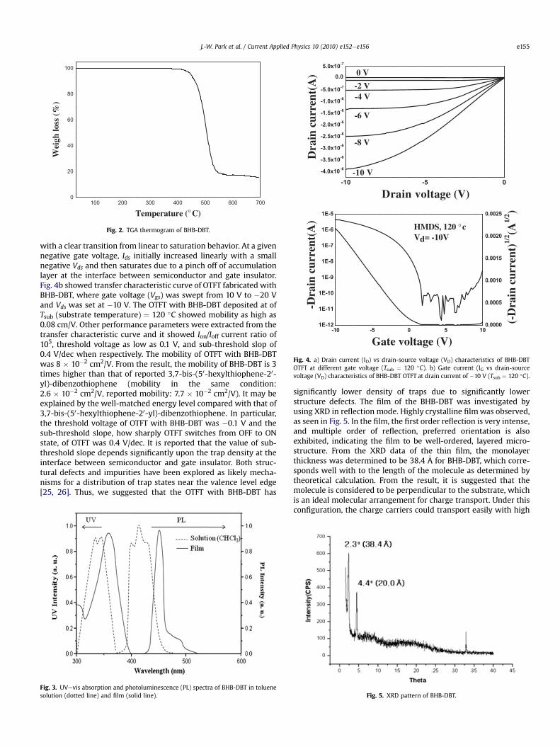
the band can not be easily oxidized and can have better stability inair. Cyclic voltammetry measurement of BHB-DBT in 0.1 M Bu4N-ClO4/acetonitril solutionwas carried out. A platinum platewas usedas the working electrode, a platinumwire as the counter electrode,and Ag/Agþ as the reference electrode. The oxidation onset peak at0.76 V for BHB-DBT leads to an estimate of highest occupiedmolecular orbital (HOMO) level of �5.16 eV. The HOMO level ofBHB-DBT is higher compared with other reported DBT derivative,although the oxidation stability is slightly decreased. However, theHOMO level of The BHB-DBT matches well with the work-functionof gold (�5.1 eV) used as a source and drain electrode. The calcu-lated charge injection barrier between source electrode is only0.6 eV for BHB-DBT. It is believed that the well-matched energylevel enhances charge injection from source electrode to BHB-DBT,and greatly improves the device performance. Top contact OTFTwas employed for electrical analysis in this study. BHB-DBT wasused as a semiconductor and silicon oxide modified with hexam-ethyldisilazane (HMDS) was used as a gate insulator. The outputcharacteristic curves [for drain current (Ids) vs drain voltage (Vds)] ofOTFT (channel length ¼ 50 mm, width ¼ 1000 mm) was shown inFig. 4a. The OTFT of BHB-DBT showed typical p-type characteristic
05-01-
-4.0x10⁻⁶
-3.5x10⁻⁶
-3.0x10⁻⁶
-2.5x10⁻⁶
-2.0x10⁻⁶
-1.5x10⁻⁶
-1.0x10⁻⁶
-5.0x10⁻⁷
0.0
5.0x10⁻⁷
-2 V
-10 V
-4 V
-6 V
-8 V
0 V
Drain voltage (V)
Dra
in c
urre
nt(A
)
-10 -5 0 5 10
1E-12
1E-11
1E-10
1E-9
1E-8
1E-7
1E-6
1E-5
0.0000
0.0005
0.0010
0.0015
0.0020
0.0025
HMDS, 120 °cVd= -10V
Gate voltage (V)
(-D
rain
curr
ent)
1/2 (A
1/2 )
-Dra
in c
urre
nt(A
)
Fig. 4. a) Drain current (ID) vs drain-source voltage (VD) characteristics of BHB-DBTOTFT at different gate voltage (Tsub ¼ 120 �C). b) Gate current (IG vs drain-sourcevoltage (VD) characteristics of BHB-DBT OTFT at drain current of �10 V (Tsub ¼ 120 �C).
100 200 300 400 500 600 7000
20
40
60
80
100
Wei
gh lo
ss (
%)
Temperature (°C)
Fig. 2. TGA thermogram of BHB-DBT.
J.-W. Park et al. / Current Applied Physics 10 (2010) e152ee156 e155
with a clear transition from linear to saturation behavior. At a givennegative gate voltage, Ids initially increased linearly with a smallnegative Vds and then saturates due to a pinch off of accumulationlayer at the interface between semiconductor and gate insulator.Fig. 4b showed transfer characteristic curve of OTFT fabricated withBHB-DBT, where gate voltage (Vgs) was swept from 10 V to �20 Vand Vds was set at �10 V. The OTFT with BHB-DBT deposited at ofTsub (substrate temperature) ¼ 120 �C showed mobility as high as0.08 cm/V. Other performance parameters were extracted from thetransfer characteristic curve and it showed Ion/Ioff current ratio of105, threshold voltage as low as 0.1 V, and sub-threshold slop of0.4 V/dec when respectively. The mobility of OTFT with BHB-DBTwas 8 � 10�2 cm2/V. From the result, the mobility of BHB-DBT is 3times higher than that of reported 3,7-bis-(50-hexylthiophene-20-yl)-dibenzothiophene (mobility in the same condition:2.6 � 10�2 cm2/V, reported mobility: 7.7 � 10�2 cm2/V). It may beexplained by the well-matched energy level compared with that of3,7-bis-(50-hexylthiophene-20-yl)-dibenzothiophene. In particular,the threshold voltage of OTFT with BHB-DBT was �0.1 V and thesub-threshold slope, how sharply OTFT switches from OFF to ONstate, of OTFT was 0.4 V/dec. It is reported that the value of sub-threshold slope depends significantly upon the trap density at theinterface between semiconductor and gate insulator. Both struc-tural defects and impurities have been explored as likely mecha-nisms for a distribution of trap states near the valence level edge[25, 26]. Thus, we suggested that the OTFT with BHB-DBT has
Fig. 3. UVevis absorption and photoluminescence (PL) spectra of BHB-DBT in toluenesolution (dotted line) and film (solid line).
significantly lower density of traps due to significantly lowerstructure defects. The film of the BHB-DBT was investigated byusing XRD in reflection mode. Highly crystalline filmwas observed,as seen in Fig. 5. In the film, the first order reflection is very intense,and multiple order of reflection, preferred orientation is alsoexhibited, indicating the film to be well-ordered, layered micro-structure. From the XRD data of the thin film, the monolayerthickness was determined to be 38.4 �A for BHB-DBT, which corre-sponds well with to the length of the molecule as determined bytheoretical calculation. From the result, it is suggested that themolecule is considered to be perpendicular to the substrate, whichis an ideal molecular arrangement for charge transport. Under thisconfiguration, the charge carriers could transport easily with high
Fig. 5. XRD pattern of BHB-DBT.

Fig. 6. AFM images of BHB-DBT.
J.-W. Park et al. / Current Applied Physics 10 (2010) e152ee156e156
mobility. An AFM image of BHB-DBT is shown in Fig. 6. Full coveringof the substrate with the material and good network interconnection between the crystallites are observed, which likelyaccount for the good charge carrier mobility measured in the OTFT.
4. Conclusion
New dibenzothiophene-based semiconducting material con-taining hexylbithiophene group was synthesized and fabricatedOTFT using this oligomer as the active layer. Due to the extended p-conjugation, efficient hole injection, and good alignment of mole-cule, BHB-DBT TFT device exhibited hole mobility of 0.08 cm/Vs,threshold voltage of �0.1 V, on/off current of 2.4 � 105, and sub-threshold slop of 0.4 V/dec when the film was deposited atTsub ¼ 120 �C, respectively. The resulting device exhibited low sub-threshold characteristic particularly desirable in low-power appli-cation for which organic semiconductor has been proposed.
Acknowledgments
Thisworkwas supportedbyagrant (F0004010-2009-32) from theInformationDisplayR&DCenter, oneof the21st Century FrontierR&DProgram funded by the Ministry of Knowledge Economy and BasicScience Research Program through theNational Research Foundation(NRF) funded by the Ministry of Education, Science and Technology(2010-0000826) and theMinistry of Knowledge Economy (MKE) andKorea Institute for Advancement in Technology (KIAT) through theWorkforce Development Program in Strategic Technology.
References
[1] M. Pope, C.E. Swenberg, Electronic Processes in Organic Crystals and Polymers,2nd ed. Oxford University Press, Oxford, 1999, 337.
[2] (a) Q. Zhao, T.H. Kim, J.W. Park, S.O. Kim, S.O. Jung, J.W. Kim, T. Ahn, Y.H. Kim,M.H. Yi, S.K. Kwon, Adv. Mater. 20 (2008) 4868;(b) H.S. Kim, Y.H. Kim, T.H. Kim, Y.Y. Noh, S. Pyo, M.H. Yi, D.Y. Kim, S.K. Kwon,Chem. Mater. 19 (2007) 3561;(c) S.J. Park, S.O. Kim, S.O. Jung, M.H. Yi, Y.H. Kim, S.K. Kwon, J. Electron. Mater.38 (2009) 2000.
[3] (a) Y. Li, T.H. Kim, Q. Zhao, E.K. Kim, S.H. Han, Y.H. Kim, J. Jang, S.K. Kwon, J.Polym. Sci., Part A: Polym. Chem. 46 (2008) 5115;(b) D.S. Chung, S.J. Lee, J.W. Park, D.B. Choi, D.H. Lee, J.W. Park, S.C. Shin,Y.H. Kim, S.K. Kwon, C.E. Park, Chem. Mater. 20 (2008) 3450;(c) T.T.M. Dang, S.J. Park, J.W. Park, D.S. Chung, C.E. Park, Y.H. Kim, S.K. Kwon,J. Polym, Sci. Part A: Polym. Chem. 45 (2007) 5277;(d) D.S. Chung, W.M. Yun, S. Nam, S.H. Kim, C.E. Park, J.W. Park, S.K. Kwon,Y.H. Kim, Appl. Phys. Lett. 94 (2009) 494;(e) J.U. Ju, D.S. Chung, S.O. Kim, S.O. Jung, C.E. Park, Y.H. Kim, S.K. Kwon, J.Polym. Sci. Part A: Polym. Chem. 47 (2009) 1609;(f) D.S. Chung, J.W. Park, S.-O. Kim, K. Heo, C.E. Park, M.R.Y.H. Kim, S.-K. Kwon,Chem. Mater. 21 (2009) 5499.
[4] H.S. Lee, D.H. Kim, J.H. Cho, Y.D. Park, J.S. Kim, K. Cho, Adv. Mater. 16 (2006)1859.
[5] A. Tsumura, H. Koezuka, T. Ando, Appl. Phys. Lett. 49 (1986) 1210.[6] C.D. Dimitrakopoulos, B.K. Furman, T. Graham, S. Hegde, S. Purushothaman,
Synth. Met. 92 (1998) 47.[7] A. Hellemans, Science 283 (1999) 771.[8] H. Moon, R. Zeis, E.J. Borkent, C. Besnard, A.J. Lovinger, T. Siegrist, C. Kloc,
Z.N. Bao, J. Am. Chem. Soc. 126 (2004) 322.[9] T. Graves-Abe, Z.N. Bao, J.C. Sturm, Nano. Lett. 4 (2004) 2489.
[10] H.E. Katz, Chem. Mater. 16 (2004) 4748.[11] H. Klauk, M. Halik, U. Zschieschang, G. Schmid, W. Radlik, W. Weber, J. Appl.
Phys. 92 (2002) 5259.[12] Z. Bao, A. Dodabalapur, A.J. Lovinger, Appl. Phys. Lett. 69 (1996) 4108.[13] G. Horowitz, M.E. Hajlaoui, Adv. Mater. 12 (2000) 1046.[14] A.L. Briseno, Q. Miao, M.M. Ling, C. Reese, H. Meng, Z. Bao, F. Wudl, J. Am.
Chem. Soc. 128 (2006) 15576.[15] K. Tankimiya, H. Ebata, K. Sakamoto, T. Izawa, T. Otsubo, Y. Kunugi, J. Am.
Chem. Soc. 128 (2006) 12604.[16] A.L. Briseno, M. Roberts, M.M. Ling, H. Moon, E.J. Nemanic, Z. Bao, J. Am. Chem.
Soc. 128 (2006) 3880.[17] K. Fujimoto, T. Hiroi, K. Kudo, M. Nakamura, Adv. Mater. 19 (2007) 525.[18] J. Locklin, M.M. Ling, A. Sung, M.E. Roberts, Z. Bao, Adv. Mater. 18 (2006) 2989.[19] H. Tian, J. Shi, D. Yan, L. Wang, Y. Geng, F. Wang, Adv. Mater. 18 (2006) 2149.[20] J. Wang, H. Wang, X. Yan, H. Huang, D. Jin, J. Shi, Y. Tang, D. Yan, Adv. Funct.
Mater. 16 (2006) 824.[21] B. Crone, A. Dodabalapur, A. Gelperin, L. Torsi, H.E. Katz, A.J. Lovinger, Z. Bao,
Appl. Phys. Lett. 78 (2001) 2229.[22] H.E. Katz, Z. Bao, S.L. Gilat, Acc. Chem. Res. 34 (2001) 359.[23] H. Meng, F. Sun, M.B. Goldfinger, G.D. Jaycox, Z. Li, W.J. Marshall,
G.S. Blackman, J. Am, Chem. Soc. 127 (2005) 2406.[24] J. Gao, L. Li, Q. Meng, R. Li, H. Jiang, H. Li, W. Hu, J. Mater. Chem. 17 (2007)
1421.[25] A.R. Volkel, R.A. Street, D. Knipp, Phys. Rev. B, Condens Matter 66 (2002)
195336.[26] N. Karl, Synth. Met. 133 (2003) 649.