growth, characterization, and thin film transistor
TRANSCRIPT
RSC Advances
PAPER
Ope
n A
cces
s A
rtic
le. P
ublis
hed
on 2
3 O
ctob
er 2
017.
Dow
nloa
ded
on 1
0/24
/202
1 9:
34:2
7 A
M.
Thi
s ar
ticle
is li
cens
ed u
nder
a C
reat
ive
Com
mon
s A
ttrib
utio
n 3.
0 U
npor
ted
Lic
ence
.
View Article OnlineView Journal | View Issue
Growth, characte
aDepartment of Physics and Institute for A
University, Kowloon Tong, Hong Kong, ChinbDepartment of Chemistry, Hong Kong Bapti
China
† Electronic supplementary informa10.1039/c7ra08699g
‡ These authors contributed equally to th
Cite this: RSC Adv., 2017, 7, 49353
Received 6th August 2017Accepted 9th October 2017
DOI: 10.1039/c7ra08699g
rsc.li/rsc-advances
This journal is © The Royal Society of C
rization, and thin film transistorapplication of CH3NH3PbI3 perovskite on polymericgate dielectric layers†
Jenner H. L. Ngai,‡ab Johnny K. W. Ho, ‡a Rocky K. H. Chan,a S. H. Cheung,a
Louis M. Leungb and S. K. So*a
Methylammonium-based perovskite compounds are generally grown on conducting or semiconducting
substrates for high performance solar cell applications. In this study, we explore the growth of these
compounds on insulators and test for their field-effect transistor performance. The key challenge is to
find a surface that favors the crystal growth of perovskites without compromising the adhesion of the
crystals. A family of methacrylate-based polymers has been identified as the insulators. Onto these
insulators, methylammonium lead iodide polycrystalline thin films were grown. Generally, we found
that the crystal size in the perovskite layers is well-correlated with the surface hydrophobicity. More
hydrophobic polymer layers favor the growth of larger crystals, but result in less favorable adhesion of
the perovskite. Methacrylate polymers with a phenyl substituent can give better adhesion and crystal
sizes despite their hydrophobic properties. Among the different insulating polymer layers, we found
that poly(phenyl methacrylate) (PPhMA), a derivative of the common commercial plastic poly(methyl
methacrylate) (PMMA), produces the best perovskite films. The molecular origin of these properties is
discussed. To test the electronic properties of these films, we employed them for thin-film
transistor applications. Under optimal conditions, the thin-film transistors fabricated on
PPhMA produce the best device with an electron mobility of 0.4 cm2 V�1 s�1. Our results are also
supported by photothermal deflection spectroscopy investigations of the subgap optical absorptions
of these films.
1 Introduction
Solution processable organic–inorganic hybrid perovskite lmshave become probably the most hotly contended material inphotovoltaics (PV) within a short span of a few years.1–3 Powerconversion efficiencies (PCEs) of perovskite-based solar cellshave surged from 3.8 to 22.1% and more.4 As high qualitypolycrystalline thin lms of perovskites are essential for PVdevices with stable and high PCEs,5 numerous studies havealready been devoted to the study of the growth of perovskitelms on conducting or semiconducting surfaces.6
Besides PV applications, perovskites should be identied asa multi-functional electronic material.7–10 Several propertiesmake the multi-functionality appealing. These include sharpoptical bandedge,7 small exciton binding energy,8 long carrier
dvanced Materials, Hong Kong Baptist
a. E-mail: [email protected]
st University, Kowloon Tong, Hong Kong,
tion (ESI) available. See DOI:
is work.
hemistry 2017
lifetime,9 and high charge carrier mobility10 to name a few.These outstanding optoelectronic properties should positionperovskite compounds for use in a wide range of devices beyondsolar cells. Conceivable examples are photodetectors, lasers,light-emitting diodes, and thin-lm transistors (TFTs). The keyadvantages of perovskite TFTs are their potential to achieve highmobility and processability. Most high performance OTFTmaterials have semi-crystalline structures or favorable intermo-lecular packing which enables effective charge hopping,11 andthese require carefully designed molecular structures andspecic processing conditions.12,13 Compared to pure OTFTs, it isrelatively easier to obtain high crystallinity perovskite-basedtransistor materials. A hole mobility of >100 cm2 V�1 s�1 andelectron mobility of >20 cm2 V�1 s�1 have been revealed inmethylammonium lead iodide perovskite single crystals,9 and theintrinsic mobility limited by the acoustic phonon scattering cango up to a few thousand cm2 V�1 s�1.14 Perovskite materials canalso be solution processed, which is particularly suitable forprinted electronics.15
Despite the appealing potential breakthrough offered byperovskite materials, the applications in TFT are still quitelimited.16–20 One of the key hurdles for the fabrication of TFTs isthe identication of a suitable dielectric layer for the growth of
RSC Adv., 2017, 7, 49353–49360 | 49353

Fig. 1 The polymers used to study the growth of the perovskite ondifferent hydrophobic surfaces.
RSC Advances Paper
Ope
n A
cces
s A
rtic
le. P
ublis
hed
on 2
3 O
ctob
er 2
017.
Dow
nloa
ded
on 1
0/24
/202
1 9:
34:2
7 A
M.
Thi
s ar
ticle
is li
cens
ed u
nder
a C
reat
ive
Com
mon
s A
ttrib
utio
n 3.
0 U
npor
ted
Lic
ence
.View Article Online
perovskite crystals.21,22 This hurdle is especially challenging forsolution processable perovskite lms for TFTs. Broadlyspeaking, gate dielectric layers can either be hydrophilic orhydrophobic. For a hydrophilic gate dielectric layer, perovskitesare known to adhere favorably.23 However, the strong interac-tions between the gate layer and perovskite prevent the growthof large crystals at the interface. The presence of small crystal-lite hinders charge carrier transport along the conductingchannel, and results in poor TFT performance. For a hydro-phobic dielectric, the wetting of the perovskite from a solutionprecursor is poor, and thus forbids the growth of any contin-uous lms, which is essential for TFTs. Thus, a compromisemust be made in terms of the hydrophobicity of the underlyinggate dielectric layer.
In this contribution, we identied several polymeric meth-acrylate (MA)-based polymers, and characterized their thin lmhydrophobicities. We then grew methylammonium lead iodide(CH3NH3PbI3) perovskite lms on these polymers using solu-tion processing techniques. The methacrylate polymers chosenwere poly(methyl methacrylate) (PMMA), poly(ethyl methacry-late) (PEMA), poly(isopropyl methacrylate) (PiPMA), poly-(isobutyl methacrylate) (PiBMA) and poly(phenyl methacrylate)(PPhMA). They possess sound thermal and chemical stability,and are available commercially. The series of methacrylatepolymers also provides a systematic way to study how surfacehydrophobicity affects the growth of perovskites. Besides theseve polymers, polystyrene (PS) was also examined as a control inorder to demonstrate the role of the methacrylate functionalgroup in the growth of the perovskite lms. The chemicalstructures of all these polymers are shown in Fig. 1. Wefound a clear correlation between the hydrophobicity and thesize and qualities of the perovskite crystals. Furthermore, wedemonstrate how to use these perovskite lms to fabricatebottom-gate top-contact TFTs having a highest mobility ofabout 0.40 cm2 V�1 s�1.
49354 | RSC Adv., 2017, 7, 49353–49360
2 Experimental
Lead(II) iodide 99% (PbI2), poly(methyl methacrylate) (PMMA),poly(ethyl methacrylate) (PEMA), poly(isobutyl methacrylate)(PiBMA), poly(phenyl methacrylate) (PPhMA), and polystyrene(PS) were purchased from Sigma Aldrich. Poly(isopropyl meth-acrylate) (PiPMA) was purchased from Polysciences, Inc. Meth-ylammonium iodide (MAI) was purchased from TokyoChemical Industry Co., Ltd (TCI). PbI2 was dissolved in dime-thylformamide (DMF) in a concentration of 450 mg mL�1 andstirred at 70 �C overnight. MAI was dissolved in isopropanol ata concentration of 45 mg mL�1 and stirred at 70 �C overnight.All perovskite lms were grown on heavily p-doped siliconsubstrates which were thermally grown with 300 nm of SiO2.The substrates were washed by sonication in deionized water,acetone, methanol and isopropanol followed by ultraviolet-ozone treatment. Aerwards, polymer solutions in chloroben-zene were spin-coated onto the substrates and dried at 100 �Cfor 1 hour in a nitrogen-lled glovebox. The dried polymer lmsserved as the substrate layer for the growth of the perovskitelms. We employed a 2-step approach to grow the perovskitelms. Firstly, PbI2 dissolved in DMF was spin-coated on top ofthe polymer layer at 1200 rpm for 60 s and was subsequentlyannealed at 70 �C for 1 hour. Solvent annealing was carried outusing the same conditions with 10 mL of DMF droplets next tothe samples, and covered with a glass Petri dish during thesolvent annealing. Secondly, the MAI solution in isopropanolwas then deposited onto the PbI2 layer at 1200 rpm for 60 s.Finally, thermal and solvent annealing were performed on thesamples using a similar procedure described above except thetemperature for annealing was 100 �C.
The hydrophobicity of the polymer lms was investigatedby contact angle measurements. The measurements werecarried out using a digital camera to capture an image ofa 5.0 mL water droplet on the thin-lm polymer. The contactangle is the angle between the tangent of the water droplet andthe wafer surface. The morphologies of the perovskite lmswere investigated using scanning electron microscopy (SEM)(LEO Gemini 1530). The average crystal size of the perovskitecrystals on different polymers was calculated automatically bythe soware ImageJ using the SEM images of the perovskitecrystal grains captured at 10000� magnication. The crystal-linity of the lms was evaluated using grazing incidence X-raydiffraction (GIXRD) with a Bruker AXS D8 Advance X-rayDiffractometer. The perovskite lms with satisfactory crystalqualities were further used for thin-lm transistor (TFT)fabrication. A bottom-gate top-contact architecture wasemployed for the TFTs. Gold (100 nm) source (S) and drain (D)electrodes were deposited via thermal evaporation througha shadow mask, dening a channel length (L) of 50 mm anda channel width (W) of 6 mm. The electrical performancemeasurements of the TFT devices were carried out in a cryostat(Oxford Instruments, Optistat DN-V) under high vacuum (10�5
Torr) and dark conditions at various temperatures andmeasured by a Keithley 236 source measurement unit togetherwith a Xantrex XT 120-0.5 as the DC gate voltage supply.
This journal is © The Royal Society of Chemistry 2017

Fig. 3 SEM images of the perovskite crystals on the polymersubstrates: (a) PMMA; (b) PEMA; (c) PiPMA (poor wetting, non-uniformfilm); (d) PiBMA (non-wetting); (e) PPhMA and (f) PS (poor adhesionwith physical pinholes).
Paper RSC Advances
Ope
n A
cces
s A
rtic
le. P
ublis
hed
on 2
3 O
ctob
er 2
017.
Dow
nloa
ded
on 1
0/24
/202
1 9:
34:2
7 A
M.
Thi
s ar
ticle
is li
cens
ed u
nder
a C
reat
ive
Com
mon
s A
ttrib
utio
n 3.
0 U
npor
ted
Lic
ence
.View Article Online
3 Results and discussion3.1 Perovskite lm growth on the polymeric insulators
Contact angle analysis of the polymeric insulators. Thesurface hydrophobicity of the polymers was assessed by contactangle measurements. The contact angle and thus the hydro-phobicity of the polymers increases in the following order:PMMA < PEMA < PiPMAz PPhMA < PiBMA < PS (Fig. 2). AmongtheMA series of polymers, PMMA is the least hydrophobic whilePiBMA is the most hydrophobic. Replacing the methyl group inPMMA with bulkier alkyl or aromatic groups enhances thehydrophobicity. Thus exposure of the O atoms in the MA groupsaffects the hydrophobicity of the polymer lms. Shielding theseO atoms with hydrophobic alkyl or phenyl groups (as in PEMA,PiPMA, PiBMA, and PPhMA) would suppress the hydrophilicity(and enhance the hydrophobicity). Thus, those polymers clearlyoffer a means to evaluate the relationship between substratehydrophobicity and perovskite crystal growth using solutionprocessing.
Morphologies of the perovskite lms. Methylammoniumlead iodide (CH3NH3PbI3) was deposited on the different poly-mers via the 2-step perovskite solution process outlined inPart 2. Fig. 3 shows the scanning electron microscopy (SEM)images of these perovskite lms. In the MA polymer series[Fig. 3(a)–(e)], compact polycrystalline lms can be clearlyobserved on all the MA polymer layers, with the exceptions ofthe PiPMA and PiBMA surfaces [Fig. 3(c) and (d)]. Close-up SEMimages in the insets of Fig. 3 further reveal the shapes andcontacts between the crystals. For the polymer surfaces withlarger crystals, the grains develop straight edges [e.g. Fig. 3(e)].Furthermore, the grain boundaries in between crystallitesappear to be tighter. Fig. 4(a) presents a summary of the averagecrystal sizes (area) on different polymers. Of all the polymerlayers, the perovskite crystals grown on the least hydrophobicPMMA have the smallest crystallites, with an average dimensionof about 0.15 mm2, and an island geometry [Fig. 3(a)]. Incontrast, the more hydrophobic PEMA and PPhMA surfacessupport larger crystal growth [Fig. 3(b) and (e)]. For PPhMA, theaverage crystal dimension is about 1.15 mm2, which is about 8
Fig. 2 Contact angles of a water droplet on the polymer substrates: (a)PMMA; (b) PEMA; (c) PiPMA; (d) PiBMA; (e) PPhMA and (f) PS.
This journal is © The Royal Society of Chemistry 2017
times larger than the crystals on PMMA. Fig. 4(b)–(d) comparethe detailed size distribution of the crystals on the MA poly-mers, with the characteristic GIXRD patterns of the lms in theESI conrming the perovskite crystals. It can be seen that thereis a correlation between the hydrophobicity and the size of theperovskite crystals. More hydrophobic MA polymers favor thegrowth of larger crystals, but for the hydrophobic PiPMA andPiBMA surfaces, the adhesions are poor [Fig. 3(c) and (d)]. Inaddition, despite the similar hydrophobicity of PiPMA andPPhMA, PPhMA gives a well-wetted perovskite lm but PiPMAgives a poorly-wetting surface. These essentially promotea motivation of understanding of crystal growth beyond surfacehydrophobicity.
Below, we briey discuss the molecular origin of crystalgrowth on the MA polymers based on the criterion of adhesionin relation to hydrophobicity and how it inuences perovskitecrystal growth. In the MA polymers, electronegative oxygenatoms and some side groups as substituents attached to theoxygen atoms can be found. An adhesion contribution by thehydrophilic O atoms can be revealed from a control experimentof the growth of perovskite crystals on PS in which O atoms aremissing. Surprisingly, comparing PPhMA and PS, perovskitecrystals with an average size of 0.57 mm2 can be observed on thePS surface with numerous pinholes, as revealed by the SEMimage [Fig. 3(f)], indicating that the crystals might not adherewell on the hydrophobic PS surface. From this, we postulate thatthe O atoms in the MA group provide initial nucleation sites tothe polymer and give better adhesion. A similar observation wasreported recently by Gratzel et al. who suggested that themethacrylate moiety can act as a support and scaffold to inducenucleation of the perovskite crystal growth.1
RSC Adv., 2017, 7, 49353–49360 | 49355

Fig. 4 (a) Relationship between contact angle and average perovskitecrystal size on different polymer substrates, with the correspondingdistribution histograms of (b) PMMA, (c) PEMA, (d) PPhMA and (e) PSsubstrates.
Fig. 5 Different interactions between the moieties in the polymersand the Pb2+ ion during the spin-coating process of PbI2 solution ontothem.
RSC Advances Paper
Ope
n A
cces
s A
rtic
le. P
ublis
hed
on 2
3 O
ctob
er 2
017.
Dow
nloa
ded
on 1
0/24
/202
1 9:
34:2
7 A
M.
Thi
s ar
ticle
is li
cens
ed u
nder
a C
reat
ive
Com
mon
s A
ttrib
utio
n 3.
0 U
npor
ted
Lic
ence
.View Article Online
The correlation between crystal size and the difference inhydrophobicity can be attributed to the substituent effect on themethacrylate polymer, in an order of methyl < ethyl < phenyl[Fig. 4(a)]. For PiPMA and PiBMA, which have isopropyl andisobutyl substituents respectively, PiPMA gives a poorly-wettingsurface where perovskite crystals can hardly form on it, result-ing in a poorly developed and non-uniform lm [Fig. 3(c)], andPiBMA simply gives a non-wetting surface for the PbI2 solution[Fig. 3(d)]. On the PiPMA and PiBMA surfaces, the alkyl groupsare so bulky that they may hinder the interactions between theO atoms on the MA polymer and the Pb2+ ions during the spin-coating process of PbI2. The longer the alkyl substituent, thegreater the steric hindrance for the O atom nucleation sites.Moreover, the electropositive hydrogen atoms in the alkylgroups could appear repulsive to the Pb2+ ions. Thus, the elec-tronic interactions between the O atoms and the Pb2+ ionswould be weakened [Fig. 5]. In other words, the bulky alkylgroups act as a barrier to the adhesion of PbI2 on the surfacesfor crystal nucleation at the early stage of PbI2 deposition,leading to poor crystal growth on such surfaces. When thesubstituents are small (e.g.methyl and ethyl), as shown in Fig. 5,the inductive effect from these electron donating groups can
49356 | RSC Adv., 2017, 7, 49353–49360
enhance the interaction between the O atoms and the Pb2+ ions,giving rise to larger crystal sizes. Here, it can be hypothesizedthat the side groups in the MA moieties can regulate the sizeand quality of the crystals during the crystal growth processwith the SEM and crystal size statistical data [Fig. 3(a), (b) and4(a)], and that the SEM results of the poorly developed lms onPiPMA and the non-wetting surface on PiBMA support the roleof the O atoms in the Pb2+ ion adhesion on the polymer surfacesby demonstrating the masking effect of the O atoms due to thebulky aliphatic isopropyl and isobutyl groups. It is also impor-tant to note that the correlation between the crystal size andsurface hydrophobicity should only be valid in the same poly-mer series.
It is worth noting that, despite the similar hydrophobicity ofPiPMA and PPhMA as observed via the contact angle measure-ments, PPhMA gave a well-wetted perovskite lm but PiPMAgave a poorly-wetting surface for perovskite growth. Therefore,compared to aliphatic substituents (e.g. methyl and ethyl),aromatic substituents (e.g. phenyl) provided better benets ofobtaining large and high quality perovskite crystals as shown inthe case of PPhMA [Fig. 4(e)]. The benecial effect of PPhMA onperovskite growth may possibly be due to the additional weakcation–p interactions between the Pb2+ ions and the phenylgroups,24,25 as shown in Fig. 5. Such interaction may assist theperovskite growth during the annealing process, and thusprovide extra support to the coordinational crystal growthbesides the polar interaction between the O atom nucleationsites and the Pb2+ ions. Therefore, the presence of both the Oatoms and the phenyl groups functioned synergistically to thecrystal growth, resulting in the highest crystal quality and thegreatest crystal size. On the other hand, the study of perovskitegrowth on the hydrophobic PS surface demonstrated the effectof the sole cation–p interactions between the phenyl groups andPb2+ ions without any O atoms as nucleation sites. The perov-skite crystals on PS could still be grown owing to the cation–pinteractions which helped nucleation. However, the cation–pinteraction is much weaker than the interaction between polarelectronegative atoms and the Pb2+ ions once the perovskitecrystal growth was completed. Thus, without the electronegativeoxygen atoms in PS, crystal adhesion is signicantly weakenedand numerous pinholes evenly distributed on the PS surfacewere found. As for PiPMA and PiBMA, with both the absence ofthe phenyl groups and the weakened polar interaction from theO atoms due to the bulky and electropositive aliphatic alkyl side
This journal is © The Royal Society of Chemistry 2017
Paper RSC Advances
Ope
n A
cces
s A
rtic
le. P
ublis
hed
on 2
3 O
ctob
er 2
017.
Dow
nloa
ded
on 1
0/24
/202
1 9:
34:2
7 A
M.
Thi
s ar
ticle
is li
cens
ed u
nder
a C
reat
ive
Com
mon
s A
ttrib
utio
n 3.
0 U
npor
ted
Lic
ence
.View Article Online
groups, Pb2+ adhesion on these surfaces on which perovskitecrystals can hardly form is found to be difficult.
In summary, our study found out the following in relation toobtaining large and quality CH3NH3PbI3 perovskite poly-crystalline lms on MA polymers: (1) electronegative O atomsare benecial to perovskite nucleation events and adhesion ofperovskite on the surface; (2) appropriate choices of aliphaticalkyl substituents in the MA group balancing the counteractinginductive effect and steric effect together with repulsivelyelectronic interactions give well-adhered and regulated largeperovskite crystal surfaces; and (3) aromatic (phenyl) substitu-ents offer cation–p interactions and help develop large perov-skite crystals.
3.2 Electronic properties of the perovskite lms
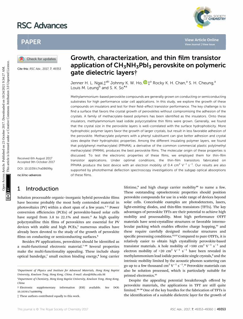
Photothermal deection spectroscopy results. To assess theelectronic properties of the perovskite lms on the differentpolymer insulators, we measured the subgap optical absorp-tions of these lms with photothermal deection spectroscopy(PDS).26 PDS is based on the mirage effect. The sample lmunder investigation is irradiated with a modulated mono-chromatic light source. Optical absorption by the samplecreates a periodic temperature rise in the surrounding medium,and in turn induces a change in the refractive index. A laserbeam directed just above the sample will be deected as a resultof the changes in the refractive index. For a small temperaturerise, the amount of deection can be shown to scale with theoptical absorption of the lm.27 With the PDS method, theoptical absorption of a semiconductor below the bandgap canbe obtained by scanning the photon energy of the incident lightsource. Details of our experimental setup have been reportedelsewhere.28
Fig. 6 shows the subgap optical absorption of the perovskitelms on the different polymers. For each absorption spectrum,a sharp drop in absorption occurs at above 1.6 eV, which
Fig. 6 Photothermal deflection spectra of the perovskite on thedifferent polymer gate dielectric surfaces. The corresponding values ofbandgap Eg and Urbach energy Eu are shown in the inset table.
This journal is © The Royal Society of Chemistry 2017
matches very well with the known energy gap of CH3NH3PbI3.29
The “steepness” of the absorption just below the bandgapenergy can be evaluated by the Urbach model:
a ¼ a0 exp
�hv� Eg
Eu
�(1)
where a0 is the absorption coefficient at the bandgap energy Eg,hv is the photon energy, and Eu is the Urbach energy. TheUrbach energy is a measure of the width of the tail of thelocalized states. A smaller Eu implies a better semiconductorand reduced localized states. The inset table in Fig. 6 comparesthe Urbach energies of the perovskite lms. It can be seen thatthe Urbach energies are 24.9, 23.0 and 22.7 meV for perovskitelms on PMMA, PEMA and PPhMA, respectively. The magni-tude of Eu suggests that the perovskite lm grown on PPhMAhas the least localized states and the smallest amount ofdefects. The PDS results are, therefore, generally consistent withthe SEM observations which show that the perovskite onPPhMA has the largest crystals. The defects observed in PDS canbe associated with reduced grain boundaries of the perovskiteon the PPhMA surface.
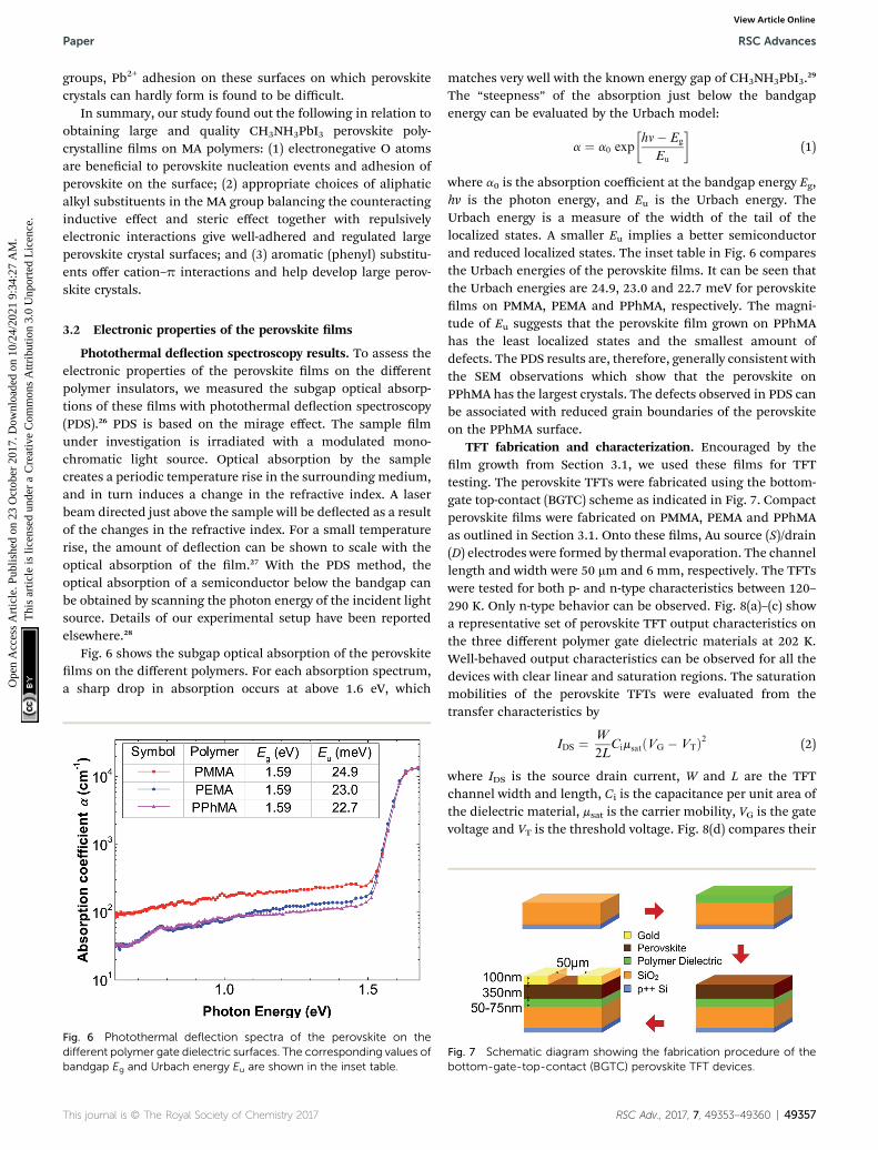
TFT fabrication and characterization. Encouraged by thelm growth from Section 3.1, we used these lms for TFTtesting. The perovskite TFTs were fabricated using the bottom-gate top-contact (BGTC) scheme as indicated in Fig. 7. Compactperovskite lms were fabricated on PMMA, PEMA and PPhMAas outlined in Section 3.1. Onto these lms, Au source (S)/drain(D) electrodes were formed by thermal evaporation. The channellength and width were 50 mm and 6 mm, respectively. The TFTswere tested for both p- and n-type characteristics between 120–290 K. Only n-type behavior can be observed. Fig. 8(a)–(c) showa representative set of perovskite TFT output characteristics onthe three different polymer gate dielectric materials at 202 K.Well-behaved output characteristics can be observed for all thedevices with clear linear and saturation regions. The saturationmobilities of the perovskite TFTs were evaluated from thetransfer characteristics by
IDS ¼ W
2LCimsatðVG � VTÞ2 (2)
where IDS is the source drain current, W and L are the TFTchannel width and length, Ci is the capacitance per unit area ofthe dielectric material, msat is the carrier mobility, VG is the gatevoltage and VT is the threshold voltage. Fig. 8(d) compares their
Fig. 7 Schematic diagram showing the fabrication procedure of thebottom-gate-top-contact (BGTC) perovskite TFT devices.
RSC Adv., 2017, 7, 49353–49360 | 49357
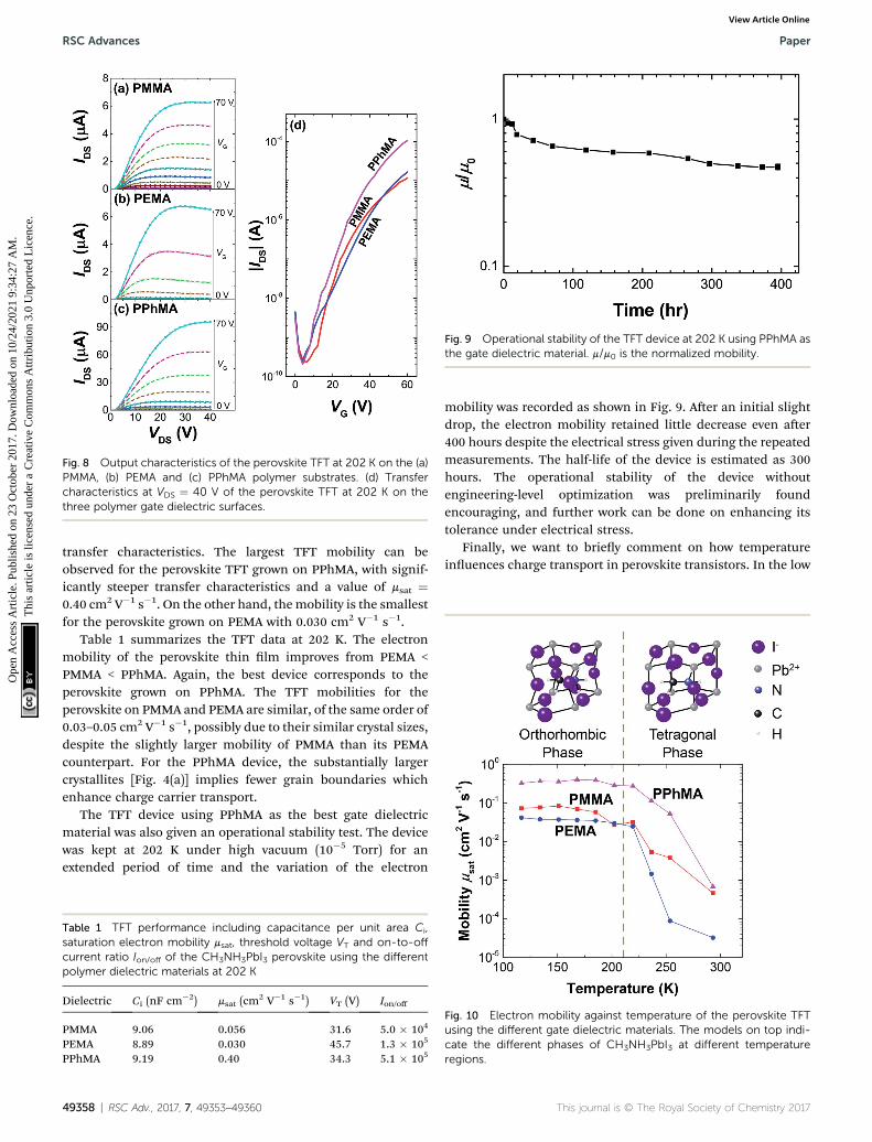
Fig. 8 Output characteristics of the perovskite TFT at 202 K on the (a)PMMA, (b) PEMA and (c) PPhMA polymer substrates. (d) Transfercharacteristics at VDS ¼ 40 V of the perovskite TFT at 202 K on thethree polymer gate dielectric surfaces.
Fig. 9 Operational stability of the TFT device at 202 K using PPhMA asthe gate dielectric material. m/m0 is the normalized mobility.
RSC Advances Paper
Ope
n A
cces
s A
rtic
le. P
ublis
hed
on 2
3 O
ctob
er 2
017.
Dow
nloa
ded
on 1
0/24
/202
1 9:
34:2
7 A
M.
Thi
s ar
ticle
is li
cens
ed u
nder
a C
reat
ive
Com
mon
s A
ttrib
utio
n 3.
0 U
npor
ted
Lic
ence
.View Article Online
transfer characteristics. The largest TFT mobility can beobserved for the perovskite TFT grown on PPhMA, with signif-icantly steeper transfer characteristics and a value of msat ¼0.40 cm2 V�1 s�1. On the other hand, themobility is the smallestfor the perovskite grown on PEMA with 0.030 cm2 V�1 s�1.
Table 1 summarizes the TFT data at 202 K. The electronmobility of the perovskite thin lm improves from PEMA <PMMA < PPhMA. Again, the best device corresponds to theperovskite grown on PPhMA. The TFT mobilities for theperovskite on PMMA and PEMA are similar, of the same order of0.03–0.05 cm2 V�1 s�1, possibly due to their similar crystal sizes,despite the slightly larger mobility of PMMA than its PEMAcounterpart. For the PPhMA device, the substantially largercrystallites [Fig. 4(a)] implies fewer grain boundaries whichenhance charge carrier transport.
The TFT device using PPhMA as the best gate dielectricmaterial was also given an operational stability test. The devicewas kept at 202 K under high vacuum (10�5 Torr) for anextended period of time and the variation of the electron
Table 1 TFT performance including capacitance per unit area Ci,saturation electron mobility msat, threshold voltage VT and on-to-offcurrent ratio Ion/off of the CH3NH3PbI3 perovskite using the differentpolymer dielectric materials at 202 K
Dielectric Ci (nF cm�2) msat (cm2 V�1 s�1) VT (V) Ion/off
PMMA 9.06 0.056 31.6 5.0 � 104
PEMA 8.89 0.030 45.7 1.3 � 105
PPhMA 9.19 0.40 34.3 5.1 � 105
49358 | RSC Adv., 2017, 7, 49353–49360
mobility was recorded as shown in Fig. 9. Aer an initial slightdrop, the electron mobility retained little decrease even aer400 hours despite the electrical stress given during the repeatedmeasurements. The half-life of the device is estimated as 300hours. The operational stability of the device withoutengineering-level optimization was preliminarily foundencouraging, and further work can be done on enhancing itstolerance under electrical stress.
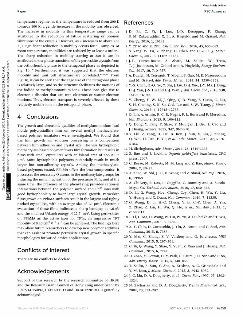
Finally, we want to briey comment on how temperatureinuences charge transport in perovskite transistors. In the low
Fig. 10 Electron mobility against temperature of the perovskite TFTusing the different gate dielectric materials. The models on top indi-cate the different phases of CH3NH3PbI3 at different temperatureregions.
This journal is © The Royal Society of Chemistry 2017
Paper RSC Advances
Ope
n A
cces
s A
rtic
le. P
ublis
hed
on 2
3 O
ctob
er 2
017.
Dow
nloa
ded
on 1
0/24
/202
1 9:
34:2
7 A
M.
Thi
s ar
ticle
is li
cens
ed u
nder
a C
reat
ive
Com
mon
s A
ttrib
utio
n 3.
0 U
npor
ted
Lic
ence
.View Article Online
temperature regime, as the temperature is reduced from 200 Ktowards 100 K, a gentle increase in the mobility was observed.The increase in mobility in this temperature range can beattributed to the reduction of lattice scattering or phononvibrations of the crystals. However, as T increases to above 250K, a signicant reduction in mobility occurs for all samples. Atroom temperature, mobilities are reduced by at least 2 orders.The sharp reduction in mobility starting at 250 K can beattributed to the phase transition of the perovskite crystals fromthe orthorhombic phase to the tetragonal phase as depicted inFig. 10.19 Furthermore, it was suggested that the electronmobility and unit cell structure are correlated.14,30,31 FromFig. 10, it can be seen that the cage size of the tetragonal phaseis relatively large, and so the structure facilitates the motions ofthe iodide or methylammonium ions. These ions give rise toelectronic disorder that can trap electrons or scatter electronmotions. Thus, electron transport is severely affected by theserelatively mobile ions in the tetragonal phase.
4 Conclusions
The growth and electronic qualities of methylammonium leadiodide polycrystalline lm on several methyl methacrylate-based polymer insulators were investigated. We found thatthe lm growth via solution processing is a competitionbetween lm adhesion and crystal size. The less hydrophobicmethacrylate-based polymer favors lm formation but results inlms with small crystallites with an island area of about 0.2mm2. More hydrophobic polymers potentially result in muchlarger but non-adhering crystals. Among the methacrylate-based polymers tested, PPhMA offers the best compromise. Itpossesses the necessary O atoms in the methacrylate groups forinducing the initial nucleation of the precursor PbI2, and at thesame time, the presence of the phenyl ring provides cation–pinteractions between the polymer surface and Pb2+ ions withgood hydrophobicity to favor large crystal growth. Perovskitelms grown on PPhMA surfaces result in the largest and tightlypacked crystallites, with an average size of 1.1 mm2. Electronicevaluation of these lms indicates a sharp bandgap at 1.6 eVand the smallest Urbach energy of 22.7 meV. Using perovskiteson PPhMA as the active layer for TFTs, an impressive TFTmobility of 0.40 cm2 V�1 s�1 can be achieved. The ndings heremay allow future researchers to develop new polymer additivesthat can assist or promote perovskite crystal growth in specicmorphologies for varied device applications.
Conflicts of interest
There are no conicts to declare.
Acknowledgements
Support of this research by the research committee of HKBUand the Research Grant Council of Hong Kong under Grant #’sFRG2/14-15/092, HKBU211913 and HKBU12201914 is gratefullyacknowledged.
This journal is © The Royal Society of Chemistry 2017
References
1 D. Bi, C. Yi, J. Luo, J.-D. Decoppet, F. Zhang,S. M. Zakeeruddin, X. Li, A. Hagfeldt and M. Gratzel, Nat.Energy, 2016, 1, 16142.
2 Y. Zhao and K. Zhu, Chem. Soc. Rev., 2016, 45, 655–689.3 S. Yang, W. Fu, Z. Zhang, H. Chen and C.-Z. Li, J. Mater.Chem. A, 2017, 5, 11462–11482.
4 J.-P. Correa-Baena, A. Abate, M. Saliba, W. Tress,T. J. Jacobsson, M. Gratzel and A. Hagfeldt, Energy Environ.Sci., 2017, 10, 710–727.
5 A. Dualeh, N. Tetreault, T. Moehl, P. Gao, M. K. Nazeeruddinand M. Gratzel, Adv. Funct. Mater., 2014, 24, 3250–3258.
6 Y.-X. Chen, Q.-Q. Ge, Y. Shi, J. Liu, D.-J. Xue, J.-Y. Ma, J. Ding,H.-J. Yan, J.-S. Hu and L.-J. Wan, J. Am. Chem. Soc., 2016, 138,16196–16199.
7 Y. Cheng, H.-W. Li, J. Qing, Q.-D. Yang, Z. Guan, C. Liu,S. H. Cheung, S. K. So, C.-S. Lee and S.-W. Tsang, J. Mater.Chem. A, 2016, 4, 12748–12755.
8 Q. Lin, A. Armin, R. C. R. Nagiri, P. L. Burn and P. Meredith,Nat. Photonics, 2015, 9, 106–112.
9 Q. Dong, Y. Fang, Y. Shao, P. Mulligan, J. Qiu, L. Cao andJ. Huang, Science, 2015, 347, 967–970.
10 Y. Liu, Z. Yang, D. Cui, X. Ren, J. Sun, X. Liu, J. Zhang,Q. Wei, H. Fan, F. Yu, et al., Adv. Mater., 2015, 27, 5176–5183.
11 H. Sirringhaus, Adv. Mater., 2014, 26, 1319–1335.12 Z. Bao and J. Locklin, Organic eld-effect transistors, CRC
press, 2007.13 C. Reese, M. Roberts, M. M. Ling and Z. Bao, Mater. Today,
2004, 7, 20–27.14 T. Zhao, W. Shi, J. Xi, D. Wang and Z. Shuai, Sci. Rep., 2016,
6, 19968.15 A. Chilvery, S. Das, P. Guggilla, C. Brantley and A. Sunda-
Meya, Sci. Technol. Adv. Mater., 2016, 17, 650–658.16 D. Li, G. Wang, H.-c. Cheng, C.-y. Chen, H. Wu, Y. Liu,
Y. Huang and X. Duan, Nat. Commun., 2016, 7, 11330.17 G. Wang, D. Li, H.-C. Cheng, Y. Li, C.-Y. Chen, A. Yin,
Z. Zhao, Z. Lin, H. Wu, Q. He, et al., Sci. Adv., 2015, 1,e1500613.
18 F. Li, C. Ma, H. Wang, W. Hu, W. Yu, A. D. Sheikh and T. Wu,Nat. Commun., 2015, 6, 8238.
19 X. Y. Chin, D. Cortecchia, J. Yin, A. Bruno and C. Soci, Nat.Commun., 2015, 6, 7383.
20 Y. Mei, C. Zhang, Z. V. Vardeny and O. Jurchescu, MRSCommun., 2015, 5, 297–301.
21 C. Bi, Q. Wang, Y. Shao, Y. Yuan, Z. Xiao and J. Huang, Nat.Commun., 2015, 6, 7747.
22 D. Zhao, M. Sexton, H.-Y. Park, G. Baure, J. C. Nino and F. So,Adv. Energy Mater., 2015, 5, 1401855.
23 T. Salim, S. Sun, Y. Abe, A. Krishna, A. C. Grimsdale andY. M. Lam, J. Mater. Chem. A, 2015, 3, 8943–8969.
24 J. C. Ma, D. A. Dougherty, et al., Chem. Rev., 1997, 97, 1303–1324.
25 N. Zacharias and D. A. Dougherty, Trends Pharmacol. Sci.,2002, 23, 281–287.
RSC Adv., 2017, 7, 49353–49360 | 49359

RSC Advances Paper
Ope
n A
cces
s A
rtic
le. P
ublis
hed
on 2
3 O
ctob
er 2
017.
Dow
nloa
ded
on 1
0/24
/202
1 9:
34:2
7 A
M.
Thi
s ar
ticle
is li
cens
ed u
nder
a C
reat
ive
Com
mon
s A
ttrib
utio
n 3.
0 U
npor
ted
Lic
ence
.View Article Online
26 W. B. Jackson, N. M. Amer, A. Boccara and D. Fournier, Appl.Opt., 1981, 20, 1333–1344.
27 A. Boccara, W. Jackson, N. M. Amer and D. Fournier, Opt.Lett., 1980, 5, 377–379.
28 C. H. Y. Ho, S. H. Cheung, H.-W. Li, K. L. Chiu, Y. Cheng,H. Yin, M. H. Chan, F. So, S.-W. Tsang and S. K. So, Adv.Energy Mater., 2017, 7, 1602360.
49360 | RSC Adv., 2017, 7, 49353–49360
29 G. E. Eperon, S. D. Stranks, C. Menelaou, M. B. Johnston,L. M. Herz and H. J. Snaith, Energy Environ. Sci., 2014, 7,982–988.
30 S. P. Senanayak, B. Yang, T. H. Thomas, N. Giesbrecht,W. Huang, E. Gann, B. Nair, K. Goedel, S. Guha, X. Moya,et al., Sci. Adv., 2017, 3, e1601935.
31 P. S. Whiteld, N. Herron, W. E. Guise, K. Page, Y. Q. Cheng,I. Milas and M. K. Crawford, Sci. Rep., 2016, 6, 35685.
This journal is © The Royal Society of Chemistry 2017