ieee sensors journal, vol. 15, no. 7, july … · the fabrication process and electromechanical...
TRANSCRIPT

IEEE SENSORS JOURNAL, VOL. 15, NO. 7, JULY 2015 3819
Ultraflexible Tactile Piezoelectric Sensor Basedon Low-Temperature Polycrystalline Silicon
Thin-Film Transistor TechnologyFrancesco Maita, Luca Maiolo, Antonio Minotti, Alessandro Pecora, Davide Ricci,
Giorgio Metta, Senior Member, IEEE, Graziella Scandurra, Gino Giusi,Carmine Ciofi, and Guglielmo Fortunato
Abstract— In this paper, we present an ultraflexible tactilesensor, in a piezo-eletricoxide-semiconductor FET configuration,composed by a poly[vinylidenefluoride-co-trifluoroethylene]capacitor with an embedded readout circuitry, based on nMOSpolysilicon electronics, integrated directly on polyimide. Theultraflexible device is designed according to an extended gate con-figuration. The sensor exhibits enhanced piezoelectric properties,thanks to the optimization of the poling procedure (with electricfield up to 3 MV/cm), reaching a final piezoelectric coefficientd33 of 47 pC/N. The device has been electromechanically testedby applying perpendicular forces with a minishaker. The tactilesensor, biased in a common-source arrangement, shows a linearresponse to increasing sinusoidal stimuli (up to 2 N) andincreasing operating frequencies (up to 1200 Hz), obtaining aresponse up to 430 mV/N at 200 Hz for the sensor with thehighest value of d33. The sensor performances were also testedafter several cycles of controlled bending in different amount ofhumidity with the intent to investigate the device behavior in realconditions.
Index Terms— Piezoelectric-oxide-semiconductor field effecttransistor (POSFET), polysilicon TFT, poly[vinylidenefluoride-co-trifluoroethylene] (PVDF-TrFE), tactile sensor, ultra-flexiblepolyimide.
I. INTRODUCTION
THE interaction between humans and robots is one of thekey challenges for the definition of new robotic behav-
ioral paradigms both in industrial sector and for humanoidmachines: indeed, the lacking of an appropriate set ofenhanced sensing capabilities would make the robots confinedto work and interact in specific controlled environments for
Manuscript received December 8, 2014; revised January 20, 2015; acceptedJanuary 26, 2015. Date of publication February 3, 2015; date of current versionMay 13, 2015. This work was supported by the Italian Institute of Technology,Genoa, Italy. The associate editor coordinating the review of this paper andapproving it for publication was Dr. Hsiao-Wen Zan.
F. Maita, L. Maiolo, A. Minotti, A. Pecora, and G. Fortunato are withthe Consiglio Nazionale delle Ricerche-Istituto per la Microelettronica eMicrosistemi, Rome 00133, Italy (e-mail: [email protected];[email protected]; [email protected]; [email protected];[email protected]).
D. Ricci and G. Metta are with the Department of Robotics, Brainand Cognitive Sciences, Istituto Italiano di Tecnologia, Genoa 16163, Italy(e-mail: [email protected]; [email protected]).
G. Scandurra, G. Giusi, and C. Ciofi is with the Dipartimento di IngegneriaElettronica, Chimica e Ingegneria Industriale, Messina 98166, Italy (e-mail:[email protected]; [email protected]; [email protected]).
Color versions of one or more of the figures in this paper are availableonline at http://ieeexplore.ieee.org.
Digital Object Identifier 10.1109/JSEN.2015.2399531
security reasons, thus minimizing the risk of damaging objectsor even cause injuries to bystanders. At the moment, thereare no official standards for human-robot interaction (HRI)in a fenceless scenario [1], [2] and, in particular, a reliableclose loop system formed by advanced wearable sensing tech-nologies and a highly robust wireless/wired protocol with safecomputation over a standard Ethernet IP is not yet available.One of the issues in HRI is the implementation of large areasensors networks that could enrich the robot skills, giving amore complete information as a result of the merging of datacoming from different sensing sources (vision, sense of touch,hearing, etc.). Especially for the sense of touch, the integrationof robust, light and bendable pressure and temperature sensorsis a key aspect for the definition of a bio-inspired skin ableto reproduce the human tactile experience in terms of therange of forces, frequencies of vibration, sensor response time,spatial resolution, etc. In recent years, a variety of new touchsensing technologies using different materials and transductionmethods [3]–[5] have been introduced, giving rise to a seriesof tremendously improved designs of electronic skins suitablefor humanoid robots. Unfortunately, most of these devices arestill quite large and are fabricated on rigid substrates, so theycannot be completely integrated onto specific areas, such asrobot fingertips, where a large number of sensors are requiredon a limited and non-planar surface.
Recently, mechanically flexible touch sensors using organicFETs have been developed for large area skin type ofapplications [6], [7]. However, best organic FETs are knownto have a mobility of about 1 cm2/Vs, which limits their use tothe recording of slow varying contact forces only. On the otherhand, devices based on Piezoelectric Oxide SemiconductorField Effect Transistors (POSFET) show very good electricalperformance [8], [9], although presently limited by the useof conventional crystalline silicon MOS that does not allowdirect integration on non-planar surfaces. Moreover, theamplification and read-out electronics is an issue itself, sinceit further reduces the possibility to embed the devices intorobot fingertips. An intriguing solution to these problemscan be sought in high performing flexible electronics basedon polycrystalline silicon (polysilicon) on plastic [10], [11]combined with piezoelectric polymer such as PVDF and itscopolymers [12]. Low Temperature Polycrystalline SiliconThin Film Transistors (LTPS TFTs) fabricated on plastic
1530-437X © 2015 IEEE. Personal use is permitted, but republication/redistribution requires IEEE permission.See http://www.ieee.org/publications_standards/publications/rights/index.html for more information.

3820 IEEE SENSORS JOURNAL, VOL. 15, NO. 7, JULY 2015
Fig. 1. POSTFT extended gate architecture. In evidence, the transistor(on the left) and the poled piezocapacitor (on the right) connected throughthe gate metal layer.
have been successfully used in different applications suchas low-cost sensor devices [13] and active matrix organiclight emitting displays [14]. Indeed, this kind of devicesexhibits excellent mechanical and electrical stability respectto amorphous silicon based TFTs and can be implemented forthe manufacturing of CMOS circuitry. In this work we presentthe fabrication process and electromechanical characterizationof a fully integrated tactile sensor based on polysiliconactive material developed on 8 μm thick polyimide substrate(POSTFT – Piezoelectric Oxide Semiconductor Thin FilmTransistor). An investigation on high electric field polingprocedure is shown to discriminate the best conditions forobtaining piezoelectric coefficient d33 greater than 45 pC/N.Moreover a detailed aging analysis of the flexible structureis presented to evaluate the sensor response and the behaviorof the piezoelectric part of the structure after several bendingcycles (up to 106) for increasing levels of relative humidity.
II. SENSOR DESIGN AND FABRICATION
A. Ultra-Flexible Tactile Element Fabrication
To reduce parasitic capacitance of the device thepiezoelectric sensing capacitor of the POSFET is usuallydirectly fabricated on top of the MOSFET (“stacked”configuration) [8], making the device fabrication more criticaland also exposing the active device to possible damage duringoperation. Since POSTFTs are made on a plastic substrate(no substrate parasitic capacitance is expected), they weredesigned according to the extended gate structure configuration(see Fig. 1), with the piezocapacitor aside the TFT. We notethat this structure is more robust and allows design flexibilityand easy passivation. To keep low the dimensions of thedevice for a future implementation on an array of sensorswith practical spatial resolution for robotic applications, werestricted the whole POSTFT area to about 2 mm2, includingmeander shaped bias resistances.
The POSTFTs were fabricated according to thenon-self-aligned architecture directly on polyimide followingthe process already described in previous works [10], [11].First, a polyimide layer, 8 μm thick, was deposited byspin-coating and cured at 350°C on an oxidized Si-wafer,used as rigid carrier. Then, an inorganic buffer layer, consistingin a sequence of low-stress Si3N4 and SiO2 films deposited atlow temperature by remote plasma techniques, was interposedbetween the polyimide and the polysilicon active layer to
Fig. 2. The polysilicon TFT transfer characteristic for a device with aW/L = 30: (a) showing a threshold voltage of abput 7 V and (b) a mobilityof 30 cm2/Vs and an on-off ratio of 106.
protect the polymer during the laser crystallization step and toprevent contamination of the active layer from the polymericsubstrate.
The polysilicon film was obtained starting from a precursorfilm of hydrogenated amorphous silicon (a-Si:H), 40 nm thick,deposited by PECVD at 250°C. To reduce the hydrogen con-tent, the film was first annealed at 350°C and then was crystal-lized by excimer laser annealing by using a specific triangular-shaped beam [15]. High quality gate dielectric 70 nm thickwas deposited at room temperature by electron cyclotronresonance plasma enhanced chemical vapor deposition(ECR-PECVD) and subsequently annealed in furnace at 300°Cfor 30 min. The electrical characteristics of TFTs withW/L = 30 are reported in Fig.2a-b, showing a field effectmobility of about 30 cm2/Vs, a threshold voltage of 7 Vand an on-off ratio of 106. Since these devices showalso good electrical stability [16] they can be suitable forthe implementation of a proper read-out interface for thepiezoelectric sensor. The devices did not show appreciablevariations in the electrical characteristics after mechanicalstress tests with bending radii up to 1.3 cm [10]. To overcomeproblems related to LTPS TFTs performance uniformity, wedecided to crystallize the a-Si:H precursor using a multi-shot laser annealing technique at low energy densities, thusobtaining small-medium grain size (around 200 nm) but higherhomogeneity in the polysilicon film. Considering the channellength (L = 20 μm) used for the POSTFT and the grainsize, the average number of grain boundaries is fairly constant

MAITA et al.: ULTRAFLEXIBLE TACTILE PIEZOELECTRIC SENSOR 3821
Fig. 3. (a) An optical microscope picture showing the piezoelectric sensorcomposed by the polysilicon TFT and the PVDF-TrFE capacitor connected tothe two resistances made also in polysilicon. (b) The picture is taken beforethe ink-jet process of the last metal layer (source and bottom electrode arestill disconnected); a picture of the same device after the detachment fromthe rigid carrier.
within the channel area, thus resulting in a lower variation ofTFT electrical performance.
Of course, the use of small-medium grain size polysiliconcompromises the device field effect mobility to values around30 cm2/Vs, which, however, are more than adequate for thePOSTFT operations and still allow integration of simple front-end circuits. After the fabrication of LTPS TFTs, the metallayer of the TFTs contacts was used also as the bottomelectrode of the PVDF-TrFE piezocapacitor. Then, a film ofabout 2 μm of PVDF-TrFE was deposited by spin coating.The solution used in the process has been obtained diluting inMEK pellets of PVDF-TrFE 70/30 bought from PIEZOTECH.The deposited layer has been annealed at 120 °C for two hours.The upper electrode was successively lithographically defined,starting from a layer of Cr 500 Å thick. The thickness ofthe evaporated metal layers were chosen in order to avoidcracks and delamination of the electrodes during the bendingtests. After this step, exploiting a sacrificial layer of Al, thePVDF-TrFE was properly patterned by reactive ion etchingin O2, to permit the bonding of the underlying layers and topassivate the structure with the PVDF itself. During this stepan opening of 100×100 μm was left in the passivation layer toallow a later connection of the source terminal of the TFT withthe top electrode of the piezocapacitor (Fig.3a). This is done toavoid the breakdown of the transistor due to the high voltageapplied during the poling process (up to 600V) between the
Fig. 4. A typical voltage ramp of the poling procedure used to enhancethe piezoelectric properties of the sensors. In red it is possible to observe theleakage currents.
top and bottom electrode, respectively connected to the gateand source terminal of the device. Finally, after the electricalpoling, a layer of silver ink is deposited by ink-jet printing toconnect these terminals. At the end of the process, the devicesfabricated on polyimide were mechanically detached from therigid carrier (see Fig.3b).
B. PVDF-TrFE Enhanced Poling Procedure
After the fabrication process, PVDF-TrFE capacitors arenormally subjected to a poling procedure in order to alignthe molecular chains of the polymer [17]. We adopted thePVDF-TrFE 70/30 ratio since this particular materialcombination provides the best piezoelectric properties,thanks to the highest crystalline fraction that can beobtained [18], [19]. To align the material dipoles typicalelectric fields <1 MV/cm are applied, achieving piezoelectriccoefficients around 28 pC/N [20]. Thanks to the optimiza-tion of the poling process in terms of ramp speed (V/s),apply/release time and temperature, we have been able to polethe devices with electric fields up to 3 MV/cm. Beyond thiselectric field value the process yield falls down because ofthe breakdown phenomena occurring in the piezo-capacitor.No tensile or compressive mechanical stress was observed onfreestanding devices. Using a Karl Suss PM5 probe stationwith micro manipulators, each device was connected to aKeithley 237 power supply to perform the poling procedure.We designed the piezoelectric capacitor so that both top andbottom electrode’s areas were smaller than PVDF-TrFE’s one,in order to prevent discharge phenomena between the twoelectrodes when high electrical fields were applied.
No electrical breakdown or evident damages wereexperimented on devices for applied electric field upto 3 MV/cm, measuring leakages current below 1A/m2
(see Fig.4). To further enhance the poling procedure, thesubstrate was heated up to 80°C and then cooled down duringthe final voltage step, according to a procedure describedin ref. [21]. We estimated the piezoelectric coefficient d33(d33 = Qp/F, where Qp is the charge developed on the

3822 IEEE SENSORS JOURNAL, VOL. 15, NO. 7, JULY 2015
Fig. 5. P(VDF-TrFE) piezoelectric coefficient values obtained for differentmaximum electric fields applied to a capacitor with a sensing material2 μm thick.
capacitor due to the applied force F), in thickness mode forthe poled P(VDF-TrFE), applying a method similar to thenormal load [22] by calculating the current collected froma RC circuit using an external resistance of 1 M� with anincoming sinusoidal stimulus of 1 N at a frequency of 200 Hz.In fact, the charge produced by piezoelectric effect, Q, can beobtained by integrating the current flowing through the loadresistor, IC:
Q(t) =∫
|IC | sin (2π f t) dt (1)
where f is the frequency of the signal. Carrying out theintegration, the d33 can be calculated as:
d33 = − |Vout |2π f R|F | (2)
where Vout is the amplitude of the voltage read with the digitaloscilloscope, R is the value of the load resistor and F is themagnitude of the mechanical stimulus. In this way we founda value of 47 pC/N (see Fig. 5), that is almost twice largerthan the commonly reported value [20].
III. RESULTS AND DISCUSSION
A. Experimental Setup
Three different experimental setups have been used tofully characterize the sensor in the electrical, mechanical andelectro-mechanical domain. At first, a Karl Suss probe stationand Keythley 236 and 237 equipped with SMU units havebeen used to obtain the DC transfer and output curves of thetransistors (Fig.2a-b). Due to the electrical connection amongthe TFT and the bias resistors and the piezoelectric capacitor,these tests have been performed before the ink-jet process,through special test pads, to avoid a non-negligible parasiticcomponent. Fig.2a and Fig.2b show respectively transfer andoutput characteristics for a device with W = 600 μm andL = 20 μm, obtaining a field effect mobility of about30 cm2/Vs and a threshold voltage or 7 V, together with anoff current below 10 pA, an on-off ratio of 106, a subthreshold
Fig. 6. (a) A block scheme of the electromechanical measurement setupand (b) a photo of the experimental setup (b). From right to left: controller,shaker, power amplifier and digital oscilloscope.
slope of about 1.2 V/dec and a leakage current through gateoxide below 10−10 A at VGS = 15V.
The electro-mechanical setup, used to verify theperformance of the whole piezoelectric sensor, is describedin Fig.6a-b.
A custom software allows to provide the frequency and themagnitude of the sinusoidal mechanical input to a controller(Bruel & Kjær - Type 7541). The generated signal is suppliedto the power amplifier (LDS – PA25E) and then to a mini-shaker (TMS – Model 2004E) that operates the transformationfrom electrical to mechanical domain. A commercial forcesensor (PCB Piezotronics – 208C01), placed co-axially respectof the vibration axis, is used as a feedback source to thecontroller in order to close the control loop and obtainstable and reliable measurements in terms of both magnitude(force error FERR < 0.5%) and frequency (frequency errorfERR < 0.2%). The output of the sensor is then acquired with adigital oscilloscope (DSO-X 3024A). Finally, the whole setupis shielded in a metallic grounded box in order to improve thesignal to noise ratio.
At last, a dedicated test system was designed andimplemented in order to validate the reliability of thepiezocapacitors over a large number of bending cycles incontrolled conditions of temperature and relative humidity.The system is built around a National Instruments PXI systemequipped with all the required boards for driving the actuatorsand acquiring/generating all the control and measurement

MAITA et al.: ULTRAFLEXIBLE TACTILE PIEZOELECTRIC SENSOR 3823
Fig. 7. (a) A simplified drawing of the test chamber for bending stresstesting and (b) a block diagram of the test system including all blocks requiredfor temperature and humidity control and for data acquisition and elaboration.
data (Fig.7b). The operation of the entire system is controlledby a dedicated software. The structure of the test chamber isshown in Fig.7a.
A bending actuator based on a servo motor (not shown inthe figure) is capable of impressing repeated bending cycles tothe samples that is placed onto a supporting polycarbonate foilunder the control of the application software. Ultra flexiblewires (not shown in the figure) allow to extract the currentpulses produced by the piezocapacitors that are fed to atransimpedance amplifier (I/V converter) for amplification,digital acquisition and analysis. A solid state temperaturesensor (LM35) and a heater are employed in order to setthe temperature inside the chamber by resorting to a softwarefeedback loop. The control of the humidity inside the chamberis obtained by controlling the temperature TW of the waterin a bubbler (Fig.7b). The saturated air at the output of thebubbler is made to flow into the chamber in such a way that itstemperature is risen to the test temperature TS prior to cominginto contact with the sample. The resulting relative humiditydepends on the temperature difference TS-TW: the higher thedifference, the lower the resulting RH. When at steady state,the system is capable of maintaining the temperature withinthe test chamber with a stability in the order of 10 mK.
The IV converter is a trans-resistance amplifier builtaround a TLC070 with very low input bias current, with a
Fig. 8. (a) Measurements of the tactile sensor using a VD = 20V, VG = 9V,RD = 270k� and RG = 1M�. On the figure is shown the AC peak-to-peakvoltage ad the drain terminal of the TFT operating a sweep of the magnitudeof the mechanical stimulus at a fixed frequency of 200Hz and (b) a sweep ofthe frequency of the input at a fixed magnitude of 1N.
trans-impedance gain of 100 M� and a bandwidth limitedto 6 Hz in order to reduce the noise at the output of the system.The control software allows to set the test temperature and thebending angle amplitude (α in Fig.7a). The signal at the outputof the I/V converter is continuously sampled and stored foron-line and off-line elaboration. Tests are typically performedat a set temperature of 40°C.
B. Electromechanical Tests
Once detached from the rigid Si carrier, the sensor has beenplaced on a flexible support of polyvinyl acetate (PVAC) tomake easier the handling of the device. Cold soldering withsilver painting has been used to place electrical connectionsbetween the POSTFT and the test instrumentation, minimizingthe length of the wires and the effect of their weight, in order toavoid unwanted vibrations of the system on the measurement.A further layer of PVAC has been placed on the top electrodeto guarantee a good insulation level of the tactile element fromthe vibrating platform. Then, a metallic finger, with a contactarea equal to the active area of the device, has been placedin contact with the top electrode of the sensor. A pre-load> 2N has been imposed on the sensor to prevent detachmentphenomena during the electromechanical tests. Before the testsa commercial sensor (FS1500NS) has been used to finelycalibrate the setup at the frequency of 200Hz, used as areference in the successive measurements.
The POSTFT has been biased in the amplification regionthrough the integrated resistances on the gate (RB = 1 M�)

3824 IEEE SENSORS JOURNAL, VOL. 15, NO. 7, JULY 2015
and the drain (RD = 270 k�) with a VD = 20 V and aVG = 9 V. Then, a sinusoidal stimulus of magnitude up to2N has been used to evaluate the performance of the sensor,obtaining the data shown in Fig.8a. The response of the sensoris linear as expected with a sensitivity @200Hz of 430mV/N.The same analysis has been performed sweeping the frequencyof the signal from 200Hz up to 1200Hz (Fig.8b). In thiscase the output voltage of the POSFET shows an high-passbehavior. This happens because of the filter that is made bythe PVDF-TrFE capacitor and the bias resistor RB. In fact,the capacitance value of the piezocapacitor, measured beforeand after the poling process with an impedance analyzer(HP 4192A), results to be in the range of 200-300 pF. Thisvalue, combined with 1M� of RB results in a cut-off frequency1/2πRBCPVDF in the range of 1÷2 kHz. It should be pointedout that the chosen common-source biasing network, althoughproviding a frequency-dependent response, allows to opti-mize the accuracy and the repeatability of the measurements.In fact, adopting the alternative floating-gate configurationwould indeed provide a frequency-independent response, butit could not allow the optimization and the stabilization ofthe quiescent point of the circuit, resulting in a non-uniformperformance from sensor to sensor and lack of repeatabilityfor successive measurements for the same sensor. It shouldbe pointed out that the dependency of the output signalfrom both force and frequency of the mechanical stimulusdoesn’t prevent the quantification of the input stimulus. In fact,by considering the linearity of the output as a function of theapplied force and the measured frequency dependence of theresponse, it is possible to post-process the data simply goingthrough a calibration phase and a fast Fourier transform of therecorded signal.
C. Reliability Tests
In order to investigate on possible degradation phenomenadue to repeated bending, the piezocapacitor has been testedusing the setup in Fig. 7a-b. In order to discern the effectson the signal due to the deterioration of the sensor from theones caused by the degradation of the electrical connectionsbetween the device and the measurement system, the samplehas been carefully prepared. At first, the piezocapacitor hasbeen placed on a flexible carrier of polycarbonate (PC).Ultra-flexible copper wires with a high number of conductorshave been used for the electrical connections to have the widestpossible contact area. Once soldered to the test pads usingsilver paint, the pad areas were protected by a thin layer ofsiliconic rubber (Arexons Motorsil D). This layer, having botha good flexibility and adhesion properties, allows to obtain areliable electrical contact during the bending maintaining thesample bound to the substrate. Finally, the substrate of PC hasbeen tied to the bending actuator to start the stress test.
At first, tests were performed in dry environment withthe humidity control disabled. The bending actuator wasdriven in such a way as repeatedly cause one end of the PCcarrier foil to swing from an upward position (UP) toward adownward (DW) position and vice-versa. As a result of thismovement, both tensile and compressive stress is applied tothe sample. More than 106 bending cycles were preformed
Fig. 9. Typical waveforms at the output of the I/V converter in Fig.6at different times during the test in dry air (a); test temperature is 40 °C;UP and DW mark the time at which the supporting PC foil temporarily stops inthe uppermost and lowermost positions, respectively, between UP/DW swingsand vice-versa. No significant degradation can be appreciated after severalhundred thousand bending cycles (b).
(one cycle consists in swinging the sample from positionUP to position DW and back from position DW to posi-tion UP) with a maximum bending angle α of 70 degrees,obtaining the results shown in Fig.9a-b. Since in dry air theshape of the peaks corresponding to the swings from DWto UP and from UP to DW was quite stable (Fig.9a), weselected the behavior of the positive and negative peaks vsbending cycles as indicator for the possible degradation of thepiezocapacitors. The value of the positive and negative peaksare reported in Fig.9b versus the number of bending cycles.A change of about 15% after 2.5 105 cycles is registered inthe monitoring of the voltage peaks, which indicates that nomajor degradation occurs. Indeed, the device was still workingeven after 106 cycles, pointing out the excellent reliability ofthe piezocapacitor with respect to repeated bending.
In another experiment we tested the influence of thehumidity on the reliability of the sensor, using the same setuppreviously described. We found that the signal generated bypiezoelectric effect was distorted in presence of high humiditylevels, as shown in Fig.10, so that the peak voltage cannot beassumed any longer as a simple indicator of the charge gener-ated during bending. Moreover, in order to avoid the high levelof RH to interfere with the IV converter, this had to be placedfurther away from the close proximity of the chamber andthis resulted in larger parasitic capacitance in parallel to thesample and, hence, in lower peaks values. To overcome theseproblems the absolute value of the charge adsorbed/suppliedduring each semi-cycle swing (UP to DW and DW to UP) wasobtained by numerical integration of the IV output waveformsaccounting for the frequency response of the system. The
MAITA et al.: ULTRAFLEXIBLE TACTILE PIEZOELECTRIC SENSOR 3825
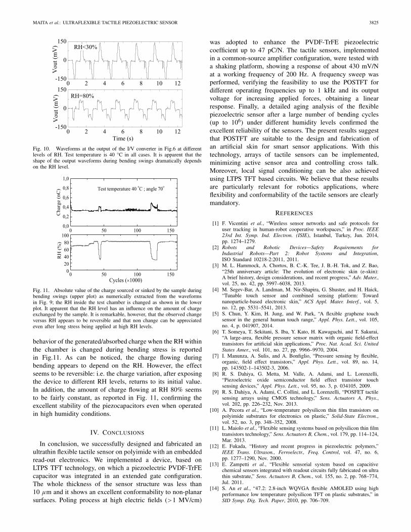
Fig. 10. Waveforms at the output of the I/V converter in Fig.6 at differentlevels of RH. Test temperature is 40 °C in all cases. It is apparent that theshape of the output waveforms during bending swings dramatically dependson the RH level.
Fig. 11. Absolute value of the charge sourced or sinked by the sample duringbending swings (upper plot) as numerically extracted from the waveformsin Fig. 9; the RH inside the test chamber is changed as shown in the lowerplot. It apparent that the RH level has an influence on the amount of chargeexchanged by the sample. It is remarkable, however, that the observed changeversus RH appears to be reversible and that non change can be appreciatedeven after long stress being applied at high RH levels.
behavior of the generated/absorbed charge when the RH withinthe chamber is changed during bending stress is reportedin Fig.11. As can be noticed, the charge flowing duringbending appears to depend on the RH. However, the effectseems to be reversible: i.e. the charge variation, after exposingthe device to different RH levels, returns to its initial value.In addition, the amount of charge flowing at RH 80% seemsto be fairly constant, as reported in Fig. 11, confirming theexcellent stability of the piezocapacitors even when operatedin high humidity conditions.
IV. CONCLUSIONS
In conclusion, we successfully designed and fabricated anultrathin flexible tactile sensor on polyimide with an embeddedread-out electronics. We implemented a device, based onLTPS TFT technology, on which a piezoelectric PVDF-TrFEcapacitor was integrated in an extended gate configuration.The whole thickness of the sensor structure was less than10 μm and it shows an excellent conformability to non-planarsurfaces. Poling process at high electric fields (>1 MV/cm)
was adopted to enhance the PVDF-TrFE piezoelectriccoefficient up to 47 pC/N. The tactile sensors, implementedin a common-source amplifier configuration, were tested witha shaking platform, showing a response of about 430 mV/Nat a working frequency of 200 Hz. A frequency sweep wasperformed, verifying the feasibility to use the POSTFT fordifferent operating frequencies up to 1 kHz and its outputvoltage for increasing applied forces, obtaining a linearresponse. Finally, a detailed aging analysis of the flexiblepiezoelectric sensor after a large number of bending cycles(up to 106) under different humidity levels confirmed theexcellent reliability of the sensors. The present results suggestthat POSTFT are suitable to the design and fabrication ofan artificial skin for smart sensor applications. With thistechnology, arrays of tactile sensors can be implemented,minimizing active sensor area and controlling cross talk.Moreover, local signal conditioning can be also achievedusing LTPS TFT based circuits. We believe that these resultsare particularly relevant for robotics applications, whereflexibility and conformability of the tactile sensors are clearlymandatory.
REFERENCES
[1] F. Vicentini et al., “Wireless sensor networks and safe protocols foruser tracking in human-robot cooperative workspaces,” in Proc. IEEE23rd Int. Symp. Ind. Electron. (ISIE), Istanbul, Turkey, Jun. 2014,pp. 1274–1279.
[2] Robots and Robotic Devices—Safety Requirements forIndustrial Robots—Part 2: Robot Systems and Integration,ISO Standard 10218-2:2011, 2011.
[3] M. L. Hammock, A. Chortos, B. C.-K. Tee, J. B.-H. Tok, and Z. Bao,“25th anniversary article: The evolution of electronic skin (e-skin):A brief history, design considerations, and recent progress,” Adv. Mater.,vol. 25, no. 42, pp. 5997–6038, 2013.
[4] M. Segev-Bar, A. Landman, M. Nir-Shapira, G. Shuster, and H. Haick,“Tunable touch sensor and combined sensing platform: Towardnanoparticle-based electronic skin,” ACS Appl. Mater. Interf., vol. 5,no. 12, pp. 5531–5541, 2013.
[5] S. Chun, Y. Kim, H. Jung, and W. Park, “A flexible graphene touchsensor in the general human touch range,” Appl. Phys. Lett., vol. 105,no. 4, p. 041907, 2014.
[6] T. Someya, T. Sekitani, S. Iba, Y. Kato, H. Kawaguchi, and T. Sakurai,“A large-area, flexible pressure sensor matrix with organic field-effecttransistors for artificial skin applications,” Proc. Nat. Acad. Sci. UnitedStates Amer., vol. 101, no. 27, pp. 9966–9970, 2004.
[7] I. Manunza, A. Sulis, and A. Bonfiglio, “Pressure sensing by flexible,organic, field effect transistors,” Appl. Phys. Lett., vol. 89, no. 14,pp. 143502-1–143502-3, 2006.
[8] R. S. Dahiya, G. Metta, M. Valle, A. Adami, and L. Lorenzelli,“Piezoelectric oxide semiconductor field effect transistor touchsensing devices,” Appl. Phys. Lett., vol. 95, no. 3, p. 034105, 2009.
[9] R. S. Dahiya, A. Adami, C. Collini, and L. Lorenzelli, “POSFET tactilesensing arrays using CMOS technology,” Sens. Actuators A, Phys.,vol. 202, pp. 226–232, Nov. 2013.
[10] A. Pecora et al., “Low-temperature polysilicon thin film transistors onpolyimide substrates for electronics on plastic,” Solid-State Electron.,vol. 52, no. 3, pp. 348–352, 2008.
[11] L. Maiolo et al., “Flexible sensing systems based on polysilicon thin filmtransistors technology,” Sens. Actuators B, Chem., vol. 179, pp. 114–124,Mar. 2013.
[12] E. Fukada, “History and recent progress in piezoelectric polymers,”IEEE Trans. Ultrason., Ferroelectr., Freq. Control, vol. 47, no. 6,pp. 1277–1290, Nov. 2000.
[13] E. Zampetti et al., “Flexible sensorial system based on capacitivechemical sensors integrated with readout circuits fully fabricated on ultrathin substrate,” Sens. Actuators B, Chem., vol. 155, no. 2, pp. 768–774,Jul. 2011.
[14] S. An et al., “47.2: 2.8-inch WQVGA flexible AMOLED using highperformance low temperature polysilicon TFT on plastic substrates,” inSID Symp. Dig. Tech. Paper, 2010, pp. 706–709.

3826 IEEE SENSORS JOURNAL, VOL. 15, NO. 7, JULY 2015
[15] V. Privitera et al., “Low-temperature annealing combined with lasercrystallization for polycrystalline silicon TFTs on polymeric substrate,”J. Electrochem. Soc., vol. 155, no. 10, pp. H764–H770, 2008.
[16] L. Maiolo et al., “Analysis of self-heating related instability in n-channelpolysilicon thin film transistors fabricated on polyimide,” Thin SolidFilms, vol. 517, no. 23, pp. 6371–6374, 2009.
[17] S. M. Nakhmanson, M. B. Nardelli, and J. Bernholc, “Ab initio studiesof polarization and piezoelectricity in vinylidene fluoride and BN-basedpolymers,” Phys. Rev. Lett., vol. 92, no. 11, p. 115504, 2004.
[18] A. J. Lovinger, “Ferroelectric polymers,” Science, vol. 220, no. 4602,pp. 1115–1121, 1983.
[19] K. Omote, H. Ohigashi, and K. Koga, “Temperature dependence ofelastic, dielectric, and piezoelectric properties of ‘single crystalline’films of vinylidene fluoride trifluoroethylene copolymer,” J. Appl. Phys.,vol. 81, no. 6, pp. 2760–2769, 1997.
[20] K. S. Ramadan, D. Sameoto, and S. Evoy, “A review of piezoelectricpolymers as functional materials for electromechanical transducers,”Smart Mater. Struct., vol. 23, no. 3, pp. 033001-1–033001-26, 2014.
[21] R. S. Dahiya, M. Valle, L. Lorenzelli, G. Metta, and S. Pedrotti,“Deposition, processing and characterization of P(VDF-TrFE) thinfilms for sensing applications,” in Proc. IEEE Sensors, Oct. 2008,pp. 490–493.
[22] J.-M. Liu, B. Pan, H. L. W. Chan, S. N. Zhu, Y. Y. Zhu, and Z. G. Liu,“Piezoelectric coefficient measurement of piezoelectric thin films: Anoverview,” Mater. Chem. Phys., vol. 75, nos. 1–3, pp. 12–18, 2002.
Francesco Maita received the master’s degree in electronics engineering andthe Ph.D. degree in engineering of sensorial and learning systems from theUniversity of Rome Tor Vergata, Rome, Italy, in 2009 and 2013, respectively.Since 2012, he has been a Research Fellow with the Consiglio Nazionale delleRicerche-Istituto per la Microelettronica e Microsistemi, Rome. His currentresearch is focused on the design and characterization of flexible electronicsas read-out interface for sensors.
Luca Maiolo received the master’s degree in physics and the Ph.D. degreewith a focus on realization and characterization of polysilicon-based electronicdevices on flexible substrates for electronics on plastic from the Universitàdegli studi di Roma Tre, Rome, Italy, in 2003 and 2008, respectively. From2004 to 2005, he was a Research Assistant with the Institute for Photonicsand Nanotechnologies, Rome, where he was involved in fabrication andelectrical characterization of polycrystalline thin-film transistors for large areaelectronics applications. In 2009, he joined the Department of Robotics, Brainand Cognitive Sciences, Istituto Italiano di Tecnologia, Genoa, Italy, as a Post-Doctoral Fellow, where he developed and tested tactile flexible sensors forhumanoid robot. He is currently a Researcher with the Consiglio Nazionaledelle Ricerche-Istituto per la Microelettronica e Microsistemi, Rome. Hisactivity is mainly focused on fabrication and characterization of electroniccircuits and smart sensors integrated on ultrathin flexible substrates.
Antonio Minotti received the University degree in materials sciencefrom the Università degli studi di Roma Tre, Rome, in 2002. Heis currently with the Consiglio Nazionale delle Ricerche-Istituto perla Microelettronica e Microsistemi, Rome, Italy, as a Technician. Hisresearch activities have been focused mainly on microelectromechanicalsystems, capacitive micromachined ultrasonic transducers, and recently onmicrofabrication processes and thin-film depositions on flexible substrates.
Alessandro Pecora was born in Rome, Italy, in 1962. He received the master’sdegree in physics from the University of Rome La Sapienza, Rome, in 1990,with a dissertation on solid-surface electron spectroscopy. Since 1990, he hasbeen a Research Scientist with the Consiglio Nazionale delle Ricerche-Istitutoper la Microelettronica e Microsistemi, Rome, where he is responsible for theactivity on devices for large area electronics with a specific focus on flexibleelectronics based on polycrystalline silicon and smart sensors. He participatedin several national and European projects, and is currently the Coordinatorof the robotic project on Factory Technologies for Humans Safety in theframework of the National Manufacturing Platform on the Factory of theFuture. He is a Scientific Expert with the Italian Ministry of Foreign Affairsand International Cooperation.
Davide Ricci received the M.Sc. degree in physics and the Ph.D. degree inelectronics engineering and computer science from the University of Genoa,Genoa, Italy, in 1989 and 1993, respectively.
He is currently a Team Leader with the Department of Robotics Brainand Cognitive Science, Istituto Italiano di Tecnologia, Genoa, where he issupervising the Soft Materials Design Laboratory. He has authored or co-authored over 100 papers in peer-reviewed international journals, conferenceproceedings, and books. His research interests include the integration of novel
materials —conductive polymers, nanocrystals, and carbon nanomaterials—with conventional technologies, for the development of devices, such as neuralelectrodes for brain–machine interfaces, flexible nanoactuators and sensors forrobotics, and smart interfaces for tissue engineering and prosthetics.
Giorgio Metta (M’09–SM’12) received the M.Sc. (cum laude) and Ph.D.degrees in electronics engineering from the University of Genoa, Genoa,Italy, in 1994 and 2000, respectively. He was a Post-Doctoral Associate withthe Artificial Intelligence Laboratory, Massachusetts Institute of Technology,Cambridge, MA, USA, from 2001 to 2002. He was with the University ofGenoa, and has been a Professor of Cognitive Robotics with the Universityof Plymouth, Plymouth, U.K., since 2012. He is currently the Director ofthe iCub Facility, Istituto Italiano di Tecnologia (IIT), Genoa, where hecoordinates the development of the iCub robotic platform/project. He is theDeputy Director of IIT delegate to the international relations and externalfunding. In this role, he is a member of the Board of Director of euRoboticsAISBL, the European reference organization for robotics research. He hasauthored approximately 200 scientific publications. He has been a PrincipalInvestigator and Research Scientist in about a dozen international and nationalfunded projects. His current research interests include biologically motivatedand humanoid robotics, and in particular, developing humanoid robots thatcan adapt and learn from experience.
Graziella Scandurra received the master’s degree in electronics engineeringand the Ph.D. degree in information technology from the University ofMessina, Messina, Italy, in 2001 and 2005, respectively. She is currentlya Researcher with the Dipartimento di Ingegneria Elettronica, Chimica eIngegneria Industriale, University of Messina. Her current research interestsinclude the design of dedicated and low-noise instrumentation, the character-ization, and the reliability of electron devices.
Gino Giusi received the Ph.D. degree in electronics engineering from theUniversity of Messina, Messina, Italy, in 2005. He is currently a Researcherand Professor with the Dipartimento di Ingegneria Elettronica, Universityof Messina. His main research interests include the study of electricalcharacterization techniques and reliability for solid-state electronic devices,the modeling and simulation of nanoscale CMOS transistors and memories,and the design of ultralow-noise electronic instrumentation and techniquesfor low frequency noise measurements. He has authored or co-authoredover 50 publications in peer-reviewed journals and international conferenceproceedings. He serves as a reviewer for leading journals in the field ofelectronic devices.
Carmine Ciofi received the M.S. degree in electronics engineering fromthe University of Pisa, Pisa, Italy, in 1989, and the Ph.D. degree from theScuola Superiore di Studi Universitari e Perfezionamento S. Anna, Pisa, in1993. He joined the Dipartimento di Ingegneria dell’Informazione, ElettronicaInformatica e Telecomunicazioni, University of Pisa, where he remained until1998. He is currently a Full Professor of Electronics with the Dipartimentodi Ingegneria Elettronica, University of Messina, Messina, Italy. His mainresearch interests include the characterization of electron devices and thedesign of low noise and dedicated instrumentation.
Guglielmo Fortunato is currently a Research Director and is responsiblefor the Consiglio Nazionale delle Ricerche-Istituto per la Microelettronicae Microsistemi, Roma Unit. He was a Visiting Scientist with the TokyoInstitute of Technology, Tokyo, Japan, in 1983, working with the Prof.Matsumura’s Group on a-Si:H Thin-Film Transistors (TFTs), and the GEC-Hirst Research Center, London, U.K., from 1985 to 1986, working withthe Prof. P. Migliorato’s Group on Polysilicon TFTs. His main scien-tific activity is on the physics and technology of inorganic (amorphous,microcrystalline silicon, and polycrystalline silicon) and organic (pentacene)TFTs. He has given a substantial contribution to the physics of polysiliconTFTs and has pioneered the use of excimer laser annealing for polysil-icon TFTs and ultrashallow junction formation. Recently, he focused onlow-temperature process for flexible electronics, including sensor applica-tions and microelectrode arrays for brain signal recording. He has beenresponsible for several national (nine) and European (seven) research con-tracts and also for industrial research contracts with STMicroelectronics,Philips, THALES, and GEC-Marconi. He was a part-time Professorof Semiconductor Device Physics at Roma III University, Rome, Italy,from 2001 to 2006. He has authored over 220 papers in international journalsand over 120 contributions to the proceedings of international conferences,has presented many oral communications and 35 invited talks in internationalconferences, and has authored five invited chapters on books and holdsten patents. He has been a co-organizer of the fourth E-MRS Symposium onThin Films for Large Area Electronics, and was the Chairman of the ThirdInternational Thin Film Transistor Conference (Rome, 2007) and Eurodisplay(Rome, 2009).