organic semiconductor distributed feedback laser pixels
TRANSCRIPT
Faraday DiscussionsCite this: Faraday Discuss., 2014, 174, 153
PAPER
Ope
n A
cces
s A
rtic
le. P
ublis
hed
on 0
7 A
ugus
t 201
4. D
ownl
oade
d on
12/
13/2
021
1:12
:54
AM
. T
his
artic
le is
lice
nsed
und
er a
Cre
ativ
e C
omm
ons
Attr
ibut
ion
3.0
Unp
orte
d L
icen
ce.
View Article OnlineView Journal | View Issue
Organic semiconductor distributedfeedback laser pixels for lab-on-a-chipapplications fabricated by laser-assistedreplication
Xin Liu,ab Stephan Prinz,†a Heino Besser,cd Wilhelm Pfleging,cd
Markus Wissmann,bd Christoph Vannahme,‡ba Markus Guttmann,bd
Timo Mappes,§b Sebastian Koeber,be Christian Koosbe
and Uli Lemmer*ab
Received 22nd April 2014, Accepted 3rd June 2014
DOI: 10.1039/c4fd00077c
The integration of organic semiconductor distributed feedback (DFB) laser sources into
all-polymer chips is promising for biomedical or chemical analysis. However, the
fabrication of DFB corrugations is often expensive and time-consuming. Here, we apply
the method of laser-assisted replication using a near-infrared diode laser beam to
efficiently fabricate inexpensive poly(methyl methacrylate) (PMMA) chips with spatially
localized organic DFB laser pixels. This time-saving fabrication process enables a pre-
defined positioning of nanoscale corrugations on the chip and a simultaneous
generation of nanoscale gratings for organic edge-emitting laser pixels next to
microscale waveguide structures. A single chip of size 30 mm � 30 mm can be
processed within 5 min. Laser-assisted replication allows for the subsequent addition of
further nanostructures without a negative impact on the existing photonic components.
The minimum replication area can be defined as being as small as the diode laser beam
focus spot size. To complete the fabrication process, we encapsulate the chip in PMMA
using laser transmission welding.
aLight Technology Institute (LTI), Karlsruhe Institute of Technology, 76131 Karlsruhe, Germany. E-mail: uli.
[email protected] of Microstructure Technology (IMT), Karlsruhe Institute of Technology, 76344 Eggenstein-
Leopoldshafen, GermanycInstitute for Applied Materials - Applied Materials Physics (IAM-AWP), Karlsruhe Institute of Technology,
76344 Eggenstein-Leopoldshafen, GermanydKarlsruhe Nano Micro Facility, Hermann-von-Helmholtz-Platz 1, 76344 Eggenstein-Leopoldshafen, GermanyeInstitute of Photonics and Quantum Electronics (IPQ), Karlsruhe Institute of Technology, 76131 Karlsruhe,
Germany
† Currently with TRUMPF Scientic Lasers GmbH + Co. KG, 85774 Unterfohring-Munchen, Germany.
‡ Currently with DTU Nanotech, Technical University of Denmark, 2800 Kgs. Lyngby, Denmark.
§ Currently with Carl Zeiss AG, Corporate Research and Technology, 07745 Jena, Germany.
This journal is © The Royal Society of Chemistry 2014 Faraday Discuss., 2014, 174, 153–164 | 153

Faraday Discussions PaperO
pen
Acc
ess
Art
icle
. Pub
lishe
d on
07
Aug
ust 2
014.
Dow
nloa
ded
on 1
2/13
/202
1 1:
12:5
4 A
M.
Thi
s ar
ticle
is li
cens
ed u
nder
a C
reat
ive
Com
mon
s A
ttrib
utio
n 3.
0 U
npor
ted
Lic
ence
.View Article Online
1 Introduction
Organic semiconductor distributed feedback (DFB) lasers are of particularinterest as tunable laser emitters covering the whole visible spectral range.1–5
Enabled by the efficient conversion in their active material, low threshold organicsemiconductor lasers allow for free space and integrated excitation sources inspectroscopic investigations.6–9 In particular, the integration of miniaturized laserlight sources in all-polymer lab-on-a-chip (LOC) platforms is promising for point-of-care systems.10–14 In order to realize laser pixels, technologies for local deni-tion of the active material, and for the laterally controlled fabrication of DFBstructures, have to be developed.
In terms of the gain materials, small molecules such as tris(8-hydroxyquino-line) aluminum (Alq3) doped with the laser dye 4-(dicyanomethylene)-2-methyl-6-(p-dimethylaminostyryl)-4H-pyran (DCM) compete with conjugated polymers. Theformer class of materials can be evaporated locally using shadow masking, andcan thus be combined with pre-dened grating structures. On the other hand,conjugated polymers can be processed by inexpensive solution-based techniquessuch as spin coating, dip-coating and doctor blading. These methods, however,result in an organic semiconductor layer covering the whole substrate. Lateralcontrol can be achieved using printing techniques. A particularly interestingapproach is the use of ink-jet printing. Ink-jet printing has already beensuccessfully applied to the fabrication of various organic electronic devices, suchas organic transistors,15,16 organic solar cells17,18 and organic light-emittingdiodes.19,20 We have recently successfully fabricated organic semiconductordistributed feedback laser pixels by ink-jet printing the active layer from aconjugated polymer solution. Utilizing an optimized mixture of high-boiling andlow-boiling solvents for dissolving the polymer, the ink-jet-printed lm prole isoptimized, thus creating uniformly emitting organic lasers. Such devices showlasing thresholds as low as 76 nJ per pulse and a spectrally homogeneous laseremission over large areas.21
The laterally controlled fabrication of DFB gratings for organic semiconductorlasers has only been addressed so far by using nanograting transfer to transfer thegratings onto a homogeneous gain material layer,22 and a rather complexapproach using direct electron beam lithography (EBL) on conjugated polymers.23
On the other hand, various substrate scale techniques such as laser interferencelithography (LIL)24 and nanoimprint lithography (NIL)25 are available to achievethe low-cost fabrication of high-quality DFB corrugation nanostructures on anLOC platform. Among them, NIL promises the mass-production of extremely nestructures with feature sizes down to 10 nm.26 The resolution of NIL can be furtherimproved by the fabrication of a rigid mold with sub-10 nm features.25 Nowadays,two main subjects of NIL are frequently used in the fabrication of DFB corruga-tions for organic semiconductor laser applications: thermal nanoimprintlithography (TNIL, also known as hot embossing) and UV-assisted nanoimprintlithography (UV-NIL).27–30 UV-NIL is an option to fabricate localized DFB corru-gations without negative effects on the existing structures, but it is mandatory touse special photoactive materials in the process. This limitation results in anarrow application eld in the fabrication of LOC systems. TNIL is advantageousfor parallel replication of all structures from a master stamp onto a common
154 | Faraday Discuss., 2014, 174, 153–164 This journal is © The Royal Society of Chemistry 2014

Paper Faraday DiscussionsO
pen
Acc
ess
Art
icle
. Pub
lishe
d on
07
Aug
ust 2
014.
Dow
nloa
ded
on 1
2/13
/202
1 1:
12:5
4 A
M.
Thi
s ar
ticle
is li
cens
ed u
nder
a C
reat
ive
Com
mon
s A
ttrib
utio
n 3.
0 U
npor
ted
Lic
ence
.View Article Online
polymer substrate. Nevertheless, it has three major drawbacks. First is the diffi-culty in the fabrication of pre-dened partial structures from a rigid master stampwith structures for different purposes. Secondly, the large-area heating can bedetrimental for existing LOC passive photonic elements and microuidic chan-nels. The third issue is the long heating and cooling time.
These limitations of TNIL can be overcome using a near-infrared high-powerdiode laser beam.31,32 In this work, we demonstrate a novel laser-assisted repli-cation to fabricate localized surface-emitting (2nd order) and edge-emitting (1storder) organic distributed DFB laser pixels on a poly(methyl methacrylate)(PMMA) substrate. Our technique allows for fast replication with standard TNILmaterials due to the localized heating. Not only is the process time reduced, thelocalized heating also provides the unique benet to replicate only parts of theexisting structures on a master stamp. Additionally, since only the dened areasare to be heated, it allows for subsequent additive fabrication of DFB corrugationswhile all the other areas are retained. The minimum localized replication areaand the inuence of the process parameters on corrugation quality are investi-gated. A functional LOC is nished aer encapsulation via laser transmissionwelding, protecting the device from air and water.33–35
2 Fabrication process
In laser-assisted replication, a rigid mold, e.g., a silicon master stamp, is pressedunder a polymer substrate, and the contact area is subsequently heated up by anear-infrared laser beam from above, as shown in Fig. 1(a). Due to heatconduction, the temperature of the polymer material, which is in direct contact
Fig. 1 (a) Scheme of the laser-assisted replication process: positioning of the PMMAsubstrate on a silicon master stamp (top), execution of the replication (middle), anddetachment of the sample (bottom). (b) Schematic illustration (left) and photograph (right)of the applied laser system.
This journal is © The Royal Society of Chemistry 2014 Faraday Discuss., 2014, 174, 153–164 | 155

Faraday Discussions PaperO
pen
Acc
ess
Art
icle
. Pub
lishe
d on
07
Aug
ust 2
014.
Dow
nloa
ded
on 1
2/13
/202
1 1:
12:5
4 A
M.
Thi
s ar
ticle
is li
cens
ed u
nder
a C
reat
ive
Com
mon
s A
ttrib
utio
n 3.
0 U
npor
ted
Lic
ence
.View Article Online
with the master stamp, increases. When the temperature exceeds the polymerglass transition temperature, the nanostructures on the rigid mold are replicatedinto the polymer substrate. Aer cooling down, the polymer substrate is detachedfrom the rigid mold, while the nanostructures are preserved.
To perform the experiments, a high-power diode laser system (Fisba Optik, FLSIron High Power Diode) with an emission wavelength of 940 nm and a maximalpower of 50 W is used. As shown in Fig. 1(b), the diode laser and a pyrometer,which provides in situ monitoring of the temperature at the laser focus plane, areintegrated within the laser scanner unit. The PMMA substrate and the siliconmaster stamp are xed in a pneumatic stage, applying a constant pressure. Thereare two basic operation modes of the system: constant laser power or constantheating temperature. In our case, the temperature regulation is chosen in order toachieve a homogeneous temperature distribution at the contact surface. Utilizingan F-Theta objective lens (Fisba Optik) with a focal length of 163 mm, the size ofthe elliptical laser focus spot on the work plane is 0.55 mm � 0.7 mm. Attributedto the applied scanner system, the maximum laser processing area can reach100 mm � 100 mm.
Before replication, a silicon master stamp was fabricated. Via electron beamlithography and reactive ion etching (RIE), the DFB corrugations with gratingperiods ranging from 195 nm to 450 nm, a height of �120 nm and a duty cycle of75% were generated. Via aligned UV-lithography and subsequent RIE on the samewafer, basins for the DFB lasers with a height of 1.2 mm were completed. A thinanti-adhesion layer was then deposited on the wafer to facilitate the polymersubstrate detachment.13
For the replication process, a 2 mm-thick PMMA substrate (Evonik, Plexiglas®XT) with a size of 30 mm � 30 mm was positioned on selected corrugations of thesilicon master stamp. The following process parameters resulted in the highest-quality replication: a heating temperature of T ¼ 180 �C, a laser scan velocity ofv ¼ 40 mm s�1, a clamping pressure of p ¼ 0.1 MPa and a hatch distance (offsetbetween two neighboring laser tracks) of Dx¼ 300 mm. To achieve a homogeneousreplication, each substrate was treated twice by the laser beam: rstly perpen-dicular to the grating orientation, as shown in Fig. 1(a), and secondly parallel tothe grating orientation. The replication process took about 5 min for the
Fig. 2 (a) Microscope image of a one-dimensional PMMA DFB grating with a period ofL ¼ 400 nm fabricated by laser-assisted replication. (b) Scanning electron microscopeimage of the grating structures fabricated by laser-assisted replication. For comparison, (c)shows a scanning electron microscope image of the L ¼ 400 nm grating structures fabri-cated by thermal nanoimprint lithography (equipment built by Institute of MicrostructureTechnology-KIT) using the same siliconmaster stamp as for (b). A temperature of 180 �C anda pressure of 1.85 MPa were applied for 15 min. The total TNIL process lasted for �45 min.
156 | Faraday Discuss., 2014, 174, 153–164 This journal is © The Royal Society of Chemistry 2014
Paper Faraday DiscussionsO
pen
Acc
ess
Art
icle
. Pub
lishe
d on
07
Aug
ust 2
014.
Dow
nloa
ded
on 1
2/13
/202
1 1:
12:5
4 A
M.
Thi
s ar
ticle
is li
cens
ed u
nder
a C
reat
ive
Com
mon
s A
ttrib
utio
n 3.
0 U
npor
ted
Lic
ence
.View Article Online
replication of an area of 40 mm � 40 mm. Aer replication, the clamping pres-sure was released. The PMMA substrate was cooled down with a nitrogen spraygun and separated from the silicon master stamp. Fig. 2(a) and (b) show amicroscope image and a scanning electron microscope image on PMMA of agrating with a period of L ¼ 400 nm. The grating structures fabricated via laser-assisted replication show a high delity over the whole molding area. The repli-cated quality was similar to thermal nanoimprint lithography, as shown inFig. 2(c). However, the laser-assisted replication process took a much shorter timecompared to the 45 min-long TNIL process. Alq3 doped with the laser dye DCMhas been chosen as the active material. It forms a very efficient Forster energytransfer system and exhibits an excellent long-term stability. Evaporating 250 nmAlq3 doped with 2.8 wt% DCM onto the dened grating elds nally yielded theorganic DFB laser pixels. The used stencil shadow mask was fabricated by UV-lithography and nickel electroplating.14
3 DFB laser characterization
For optical characterization, the fabricated surface-emitting organic DFB laserswere excited by a diode-pumped, actively Q-switched frequency tripled neo-dymium:yttrium orthovanadate (Nd:YVO4) laser (Advanced Optical TechnologyLtd., AOT-YVO-20QSP) with a wavelength of 355 nm. The pump pulse had aduration of approximately 1 ns at a repetition rate of 1 kHz. The pump pulseenergy was adjusted with a variable neutral density lter and measured with acalibrated gallium arsenide phosphide photodiode connected to an oscilloscope(Tektronix, TDS2024C). The sample was kept in a vacuum chamber (<5� 10�3 Pa)to protect the active material from photooxidation. The chamber can be shied inthe plane perpendicular to the excitation beam using an automated precisionstage. This allows for a spectrally and spatially resolved characterization of thesamples. A focusing lens was used to adjust the excitation spot size. The emissionfrom the sample was collected using the focusing lens for the pump beam, thendirected through a dichroic mirror and coupled into a multimode optical ber.Further on, the laser spectra were analyzed using a spectrograph (Acton ResearchCorporation, SpectraPro 300i, variable grating) connected to an intensiedcharge-coupled device camera (Princeton Research, PiMax 512). The pump spotshowed a slightly elliptical shape with a size of 30 mm � 40 mm on the sample.
Fig. 3(a) shows the color-encoded spatially resolved lasing wavelength from aPMMA chip containing 9 laser pixels with individual lateral dimensions of 500 mm� 500 mm and an interspacing of 500 mm. The grating period of the DFB corru-gations varies from 370 nm to 450 nm in steps of 10 nm from the outermost lepixel to the outermost right pixel. The chip was probed with a resolution of100 mm. The laser emission wavelength did not show any deviation on the area ofa single laser pixel within the spectral resolution of the setup (approximately0.5 nm). This indicates a very uniform replication of the nanogratings in PMMA.The corresponding laser emission spectra and the laser threshold values for theTE0-modes are shown in Fig. 3(b) and (c). The blue-shied TM0-mode laser peaksidentied with a polariser can be detected at l ¼ 630.4 nm and l ¼ 643.6 nm.These peaks originate from the lasers with grating periods of L ¼ 400 nm andL ¼ 410 nm. The higher laser threshold from the laser pixel with a grating period
This journal is © The Royal Society of Chemistry 2014 Faraday Discuss., 2014, 174, 153–164 | 157

Fig. 3 (a) Color-encoded spatially resolved laser wavelengths of the fabricated organicDFB laser pixels with grating periods from 370 nm (left) to 450 nm (right) in steps of 10 nm.(b) Laser spectra and TE0-mode laser threshold corresponding to the grating distribution.For some gratings the onset of the TM0-mode can also be seen as very small peaks. (c)Input–output characteristics of a laser pixel with a grating period ofL¼ 410 nm and a laseremission at l ¼ 657.5 nm.
Faraday Discussions PaperO
pen
Acc
ess
Art
icle
. Pub
lishe
d on
07
Aug
ust 2
014.
Dow
nloa
ded
on 1
2/13
/202
1 1:
12:5
4 A
M.
Thi
s ar
ticle
is li
cens
ed u
nder
a C
reat
ive
Com
mon
s A
ttrib
utio
n 3.
0 U
npor
ted
Lic
ence
.View Article Online
of 450 nm is attributed to the lower gain coefficient at the emission wavelength of712.5 nm.
For being suitable for LOC spectroscopic applications, the organic semi-conductor lasers are usually based on rst-order DFB gratings for the emission oflight in the chip plane only. By introducing a waveguide onto the chip, the rst-order organic laser emission can be efficiently coupled and guided to the analytesites. PMMA chips with deep ultraviolet (DUV)-induced waveguides have beenfabricated previously.11,13 In this work, we fabricated the active grating andwaveguides altogether via laser-assisted replication and evaporated Alq3:DCM onboth of them to build a coupled edge-emitting organic laser on chip. This novelconguration allows for a one-step fabrication of the laser and waveguide withoutmix-and-match pattern-related defects.36 Besides, the direct connection betweenthe laser and waveguide made from the same active material will facilitate anoptimum coupling efficiency.
Different gratings with lateral dimensions of 500 mm, interconnected by300 mm-wide waveguide structures perpendicular to the grating orientation, weresimultaneously fabricated in 1.2 mm-deep basins on the PMMA chip. The gratingperiods for the rst-order organic DFB laser were chosen to be L ¼ 195 nm,L ¼ 200 nm, and L ¼ 205 nm, as marked in Fig. 4(a). A 250 nm-thick layer ofAlq3:DCM was evaporated on the dened grating and waveguide, thus allowingfor an optimum light coupling.
The experimental setup for the chip characterization is schematically depictedin Fig. 4(b). The pump laser and the detection system were the same as used forthe characterization of the surface-emitting organic lasers, but we changed thedetection plane according to the chip orientation. The excitation spot diameteron the sample surface was �100 mm. In order to limit laser degradation inthe ambient atmosphere, we set the excitation repetition rate as low as 100 Hz.Fig. 4(c) shows the laser spectrum of a DFB laser with a grating period of
158 | Faraday Discuss., 2014, 174, 153–164 This journal is © The Royal Society of Chemistry 2014

Fig. 4 (a) Microscope image of a coupled organic DFB edge-emitting laser (left) and anatomic force micrograph of the nanograting with a period of L ¼ 200 nm (right). (b)Schematic illustration of the optical setup to detect the edge emission from the integratedorganic DFB laser. (c) Laser spectrum and input–output curve (inset) taken from the chipfacet of a grating of L ¼ 200 nm using a multimode optical fiber coupled to aspectrometer.
Paper Faraday DiscussionsO
pen
Acc
ess
Art
icle
. Pub
lishe
d on
07
Aug
ust 2
014.
Dow
nloa
ded
on 1
2/13
/202
1 1:
12:5
4 A
M.
Thi
s ar
ticle
is li
cens
ed u
nder
a C
reat
ive
Com
mon
s A
ttrib
utio
n 3.
0 U
npor
ted
Lic
ence
.View Article Online
L ¼ 200 nm. The laser emission at l ¼ 645.5 nm was detected at the chip facetusing a multimode optical ber (Ocean Optics, P400-3-UV-VIS). A stronger back-ground due to the Alq3:DCM uorescence than in the case of the surface-emittinglasers is observed. This can be explained by the fact that the uorescence iscoupled into the waveguide with comparable efficiency to the laser radiation. Inthe case of surface-emitting lasers, the uorescence is almost not detected as it isemitted in all directions. The corresponding laser threshold was measured to be145 nJ per pulse. This higher threshold can be explained by the laser beingpumped at a larger excitation spot size than for the surface-emitting lasers.
4 Size dependence of laser-assisted replication
The minimum replication area size is determined by the applied laser beamdiameter, the used processing time, and the laser-induced heating temperature inthe contact zone of the master stamp and polymer. To investigate the spatialresolution limits of the replication process, we fabricated test structures with atool comprising spatially dened DFB grating areas via laser-assisted replicationusing different heating periods. Fig. 5(a) shows a microscope image of thebeginning trail of the replicated structure, which was obtained by laser-inducedheating of a single line with a scanning speed of 40 mm s�1, corresponding to a�17.5 ms-long local heating. The red line indicates a t to the right end of thereplicated structures. The rim is in good accordance with the elliptical laser focusspot size of 0.55 mm � 0.7 mm.
In comparison, applying 2 s-long punctuated heating resulted in an expansionof the heat-affected zone on the silicon stamp and a consequently enlargedreplication area. As shown in Fig. 5(b), an extension was measured as �3.8 timesthat of the laser focus spot size.
We veried the versatility of the localized replication by the fabrication of pre-selected laser pixels. Fig. 5(c) shows a partial replication from the silicon masterstamp with gratings in periods of L ¼ 390 nm, L ¼ 400 nm, L ¼ 410 nm and
This journal is © The Royal Society of Chemistry 2014 Faraday Discuss., 2014, 174, 153–164 | 159
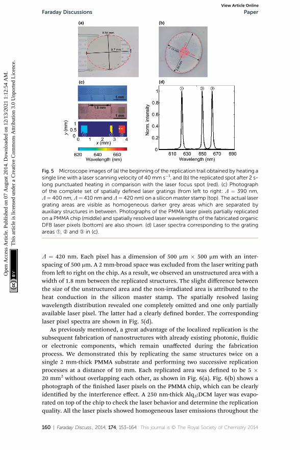
Fig. 5 Microscope images of (a) the beginning of the replication trail obtained by heating asingle line with a laser scanning velocity of 40mm s�1, and (b) the replicated spot after 2 s-long punctuated heating in comparison with the laser focus spot (red). (c) Photographof the complete set of spatially defined laser gratings (from left to right: L ¼ 390 nm,L¼ 400 nm,L¼ 410 nm andL¼ 420 nm) on a siliconmaster stamp (top). The actual lasergrating areas are visible as homogeneous darker grey areas which are separated byauxiliary structures in between. Photographs of the PMMA laser pixels partially replicatedon a PMMA chip (middle) and spatially resolved laser wavelengths of the fabricated organicDFB laser pixels (bottom) are also shown. (d) Laser spectra corresponding to the gratingareas ➀, ➁ and ➂ in (c).
Faraday Discussions PaperO
pen
Acc
ess
Art
icle
. Pub
lishe
d on
07
Aug
ust 2
014.
Dow
nloa
ded
on 1
2/13
/202
1 1:
12:5
4 A
M.
Thi
s ar
ticle
is li
cens
ed u
nder
a C
reat
ive
Com
mon
s A
ttrib
utio
n 3.
0 U
npor
ted
Lic
ence
.View Article Online
L ¼ 420 nm. Each pixel has a dimension of 500 mm � 500 mm with an inter-spacing of 500 mm. A 2 mm-broad space was excluded from the laser writing pathfrom le to right on the chip. As a result, we observed an unstructured area with awidth of 1.8 mm between the replicated structures. The slight difference betweenthe size of the unstructured area and the non-irradiated area is attributed to theheat conduction in the silicon master stamp. The spatially resolved lasingwavelength distribution revealed one completely omitted and one only partiallyavailable laser pixel. The latter had a clearly dened border. The correspondinglaser pixel spectra are shown in Fig. 5(d).
As previously mentioned, a great advantage of the localized replication is thesubsequent fabrication of nanostructures with already existing photonic, uidicor electronic components, which remain unaffected during the fabricationprocess. We demonstrated this by replicating the same structures twice on asingle 2 mm-thick PMMA substrate and performing two successive replicationprocesses at a distance of 10 mm. Each replicated area was dened to be 5 �20 mm2 without overlapping each other, as shown in Fig. 6(a). Fig. 6(b) shows aphotograph of the nished laser pixels on the PMMA chip, which can be clearlyidentied by the interference effect. A 250 nm-thick Alq3:DCM layer was evapo-rated on top of the chip to check the laser behavior and determine the replicationquality. All the laser pixels showed homogeneous laser emissions throughout the
160 | Faraday Discuss., 2014, 174, 153–164 This journal is © The Royal Society of Chemistry 2014

Fig. 6 (a) Scheme of the first and second laser-assisted replication areas of size 5 mm �20 mm. (b) Photograph of the subsequently fabricated grating structures 1 and 2. (c)Finished chip after encapsulation with a PMMA lid via laser transmission welding. The chipedge appears silver due to the absorption layer of carbon.
Paper Faraday DiscussionsO
pen
Acc
ess
Art
icle
. Pub
lishe
d on
07
Aug
ust 2
014.
Dow
nloa
ded
on 1
2/13
/202
1 1:
12:5
4 A
M.
Thi
s ar
ticle
is li
cens
ed u
nder
a C
reat
ive
Com
mon
s A
ttrib
utio
n 3.
0 U
npor
ted
Lic
ence
.View Article Online
whole pixel area with corresponding wavelengths according to their DFB gratingperiods. Laser pixels featuring the same grating period revealed comparablecharacteristics, e.g., the laser thresholds of the laser pixels with a grating period ofL ¼ 420 nm were measured to be 17.3 nJ per pulse and 14.8 nJ per pulse, bothemitting at the same laser peak wavelength of l ¼ 670 nm. The existing gratingstructures were not inuenced by the subsequent replication process. This can bewidely useful for LOC and other integrated optics applications. The inexpensivefabrication of identical nanostructures without repetitive construction on amaster stamp is shown to be possible.
5 Encapsulation via laser transmission welding
During operation, organic semiconductors suffer from photoluminescence degra-dation when exposed to air or water. Therefore, encapsulation is necessary tosustain the long lifetime of the device. Previously, LOCs containing organic semi-conductor lasers have been encapsulated in a polymer using thermal bonding,12,13
which is usually time-consuming and therefore only suitable for parallel processingwith large numbers of LOC chips. In addition, the high temperature used forbonding leads to bleaching of the organic dyes. Here, we demonstrate the encap-sulation of our fabricated organic laser chip via laser transmission welding.33 Forthis purpose, the same setup as for laser-assisted replication was used, as shown inFig. 1. A 2mm-thick PMMA substrate was prepared as a lid and placed on top of thepreviously fabricated chip with laser-pixel basins. Since PMMA is transparent tonear-infrared radiation, an additional absorption layer of carbon with a thickness of5–10 nm was deposited under the polymer chip, where the welding process was tobe performed (chip edge). Applying the diode laser beam at a wavelength of l¼ 940nm and a maximum power of 50 W on the chip edge with a 5 mm-wide margin, theabsorption layer converted the laser radiation into heat, which melted the twoPMMA substrates along the contact area and bound them together (heatingtemperature T ¼ 140 �C, laser scan velocity v ¼ 40 mm s�1; clamping pressurep ¼ 0.4 MPa, hatch distance Dx ¼ 300 mm). A photograph of the encapsulatedorganic laser chip is shown in Fig. 6(c). As expected, the encapsulation process wasfound not to affect the emission properties of the laser pixels. Laser transmissionwelding is thus not only a practical tool for chip bonding direct aer laser-assistedreplication, but also can be a substitute for thermal bonding aer the thermalnanoimprint lithography process.
This journal is © The Royal Society of Chemistry 2014 Faraday Discuss., 2014, 174, 153–164 | 161

Faraday Discussions PaperO
pen
Acc
ess
Art
icle
. Pub
lishe
d on
07
Aug
ust 2
014.
Dow
nloa
ded
on 1
2/13
/202
1 1:
12:5
4 A
M.
Thi
s ar
ticle
is li
cens
ed u
nder
a C
reat
ive
Com
mon
s A
ttrib
utio
n 3.
0 U
npor
ted
Lic
ence
.View Article Online
6 Conclusion
In summary, we have successfully applied laser-assisted replication in the fabri-cation of spatially localized organic semiconductor DFB laser pixels on PMMAchips. We accomplished nine surface-emitting laser pixels based on nanogratingswith different periods in lateral dimensions of 500 mm � 500 mm on a PMMAsubstrate. We also realized the simultaneous fabrication of nanoscale DFBcorrugations and neighboring microscale waveguide basins. Aer evaporation ofthe same active material, coupled edge-emitting organic lasers were achieved witha combination of the functional waveguides. The minimum fabrication area sizewas investigated by comparing the replication spot with the laser beam focus size,and the versatility of the spatially localized replication was veried by the fabri-cation of pre-selected laser pixels. We also proved that using this fabricationmethod, further nanostructures could be added into the chip platform without anegative inuence on the neighboring photonic components. Consequently,laser-assisted replication is an ideal tool for the fast and exible fabrication ofmicro- and nanostructures with high quality, and is especially suited for the rapidprototyping of LOC platforms. Finally, we completed the chip fabrication byencapsulation of the polymeric chip using laser transmission welding. Thisprogress in the additive fabrication of gratings can ideally be combined with ourrecent progress in ink-jet printing the active gain medium of organic semi-conductors. By using different laser pixels, this approach allows for the realizationof digitally manufactured versatile coherent light sources integrated in photonicmicrosystems and LOC devices.
Acknowledgements
The authors thank A. Bacher, P.-J. Jakobs and A. Muslija for the silicon masterstamp fabrication and P. Abaffy for taking the scanning electron microscopeimages. This work was supported by the Deutsche Forschungsgemeinscha andthe State of Baden-Wurttemberg through the DFG-Center for Functional Nano-structures (CFN). The work of X. L. is supported by Carl Zeiss Stiung andKarlsruhe School of Optics & Photonics (KSOP). We acknowledge support byDeutsche Forschungsgemeinscha and the Open Access Publishing Fund ofKarlsruhe Institute of Technology. Finally, the support for laser processing by theKarlsruhe Nano Micro Facility (KNMF, http://www.knmf.kit.edu), a Helmholtzresearch infrastructure at the Karlsruhe Institute of Technology is gratefullyacknowledged.
References
1 N. Tessler, G. J. Denton and R. H. Friend, Lasing from conjugated-polymermicrocavities, Nature, 1996, 382, 695–697.
2 F. Hide, M. A. Diaz-Garcia, B. J. Schwartz, M. R. Andersson, Q. B. Pei andA. J. Heeger, Semiconducting polymers: a new class of solid-state lasermaterials, Science, 1996, 273, 1833–1836.
3 S. V. Frolov, M. Ozaki, W. Gellermann, Z. V. Vardeny and K. Yoshino,Mirrorless lasing in conducting polymer poly(2,5-dioctyloxy-p-phenylenevinylene) lms, Jpn. J. Appl. Phys., 1996, 35, L1371–L1373.
162 | Faraday Discuss., 2014, 174, 153–164 This journal is © The Royal Society of Chemistry 2014

Paper Faraday DiscussionsO
pen
Acc
ess
Art
icle
. Pub
lishe
d on
07
Aug
ust 2
014.
Dow
nloa
ded
on 1
2/13
/202
1 1:
12:5
4 A
M.
Thi
s ar
ticle
is li
cens
ed u
nder
a C
reat
ive
Com
mon
s A
ttrib
utio
n 3.
0 U
npor
ted
Lic
ence
.View Article Online
4 I. D. W. Samuel and G. A. Turnbull, Organic semiconductor lasers, Chem. Rev.,2007, 107, 1272–1295.
5 S. Klinkhammer, X. Liu, K. Huska, Y. Shen, S. Vanderheiden, S. Valouch,C. Vannahme, S. Brase, T. Mappes and U. Lemmer, Continuously tunablesolution-processed organic semiconductor DFB lasers pumped by laserdiode, Opt. Express, 2012, 20, 6357–6364.
6 Y. Oki, S. Miyamoto, M. Maeda and N. J. Vasa, Multiwavelength distributedfeedback dye laser array and its application to spectroscopy, Opt. Lett., 2002,27, 1220–1222.
7 T. Woggon, S. Klinkhammer and U. Lemmer, Compact spectroscopy systembased on tunable organic semiconductor lasers, Appl. Phys. B, 2010, 99, 47–51.
8 S. Klinkhammer, T. Woggon, C. Vannahme, T. Mappes and U. Lemmer, Opticalspectroscopy with organic semiconductor lasers, Proc. SPIE, 2010, 7722, 77221I.
9 X. Liu, P. Stefanou, B. Wang, T. Woggon, T. Mappes and U. Lemmer, Organicsemiconductor distributed feedback (DFB) laser as excitation source in Ramanspectroscopy, Opt. Express, 2013, 21, 28941–28947.
10 T. Mappes, C. Vannahme, M. Schelb, U. Lemmer and J. Mohr, Design foroptimized coupling of organic semiconductor laser light into polymerwaveguides for highly integrated bio-photonic sensors, Microelectron. Eng.,2009, 86, 1499–1501.
11 C. Vannahme, S. Klinkhammer, A. Kolew, P.-J. Jakobs, M. Guttmann, S. Dehm,U. Lemmer and T. Mappes, Integration of organic semiconductor lasers andsingle-mode passive waveguides into a PMMA substrate, Microelectron. Eng.,2010, 87, 693–695.
12 C. Vannahme, M. B. Christiansen, T. Mappes and A. Kristensen, Optouidicdye laser in a foil, Opt. Express, 2010, 18, 9280–9285.
13 C. Vannahme, S. Klinkhammer, M. B. Christiansen, A. Kolew, A. Kristensen,U. Lemmer and T. Mappes, All-polymer organic semiconductor laser chips:parallel fabrication and encapsulation, Opt. Express, 2010, 18, 24881–24887.
14 C. Vannahme, S. Klinkhammer, U. Lemmer and T. Mappes, Plastic lab-on-a-chip for uorescence excitation with integrated organic semiconductorlasers, Opt. Express, 2011, 19, 8179–8186.
15 H. Sirringhaus, T. Kawase, R. H. Friend, T. Shimoda, M. Inbasekaran, W. Wuand E. P. Woo, High-resolution inkjet printing of all-polymer transistorcircuits, Science, 2000, 290, 2123–2126.
16 H. E. Katz, Recent advances in semiconductor performance and printingprocesses for organic transistor-based electronics, Chem. Mater., 2004, 16,4748–4756.
17 C. N. Hoth, P. Schilinsky, S. A. Choulis and C. J. Brabec, Printing highlyefficient organic solar cells, Nano Lett., 2008, 8, 2806–2813.
18 T. Aernouts, T. Aleksandrov, C. Girotto, J. Genoe and J. Poortmans, Polymerbased organic solar cells using ink-jet printed active layers, Appl. Phys. Lett.,2008, 92, 033306.
19 T. R. Hebner, C. C. Wu, D. Marcy, M. H. Lu and J. C. Sturm, Ink-jet printing ofdoped polymers for organic light emitting devices, Appl. Phys. Lett., 1998, 72,519–521.
20 J. Bharathan and Y. Yang, Polymer electroluminescent devices processed byinkjet printing: I. Polymer light-emitting logo, Appl. Phys. Lett., 1998, 72,2660–2662.
This journal is © The Royal Society of Chemistry 2014 Faraday Discuss., 2014, 174, 153–164 | 163

Faraday Discussions PaperO
pen
Acc
ess
Art
icle
. Pub
lishe
d on
07
Aug
ust 2
014.
Dow
nloa
ded
on 1
2/13
/202
1 1:
12:5
4 A
M.
Thi
s ar
ticle
is li
cens
ed u
nder
a C
reat
ive
Com
mon
s A
ttrib
utio
n 3.
0 U
npor
ted
Lic
ence
.View Article Online
21 X. Liu, S. Klinkhammer, K. Sudau, N. Mechau, C. Vannahme, J. Kaschke,T. Mappes, M. Wegener and U. Lemmer, Ink-jet-printed organicsemiconductor distributed feedback laser, Appl. Phys. Express, 2012, 5, 072101.
22 X. Liu, S. Klinkhammer, Z. Wang, T. Wienhold, C. Vannahme, P.-J. Jakobs,A. Bacher, A. Muslija, T. Mappes and U. Lemmer, Pump spot size dependentlasing threshold in organic semiconductor DFB lasers fabricated viananograting transfer, Opt. Express, 2013, 21, 27697–27706.
23 R. Stabile, A. Camposeo and L. Persano, Organic-based distributed feedbacklasers by direct electron-beam lithography on conjugated polymers, Appl.Phys. Lett., 2007, 91, 101110.
24 M. Stroisch, T. Woggon, U. Lemmer, G. Bastian, G. Violakis and S. Pissadakis,Organic semiconductor distributed feedback laser fabricated by direct laserinterference ablation, Opt. Express, 2007, 15, 3968–3973.
25 N. R. Hendricks and K. R. Carter, Nanoimprint lithography of polymers, inPolymer Science: A Comprehensive Reference, Elsevier, 2012, pp. 251–274.
26 S. Y. Chou, P. R. Krauss and P. J. Renstrom, Nanoimprint lithography, J. Vac.Sci. Technol., B: Microelectron. Nanometer Struct.–Process., Meas., Phenom.,1996, 14, 4129–4133.
27 D. Pisignano, L. Persano, P. Visconti, R. Cingolani, G. Gigli, G. Barbarella andL. Favaretto, Oligomer-based organic distributed feedback lasers by room-temperature nanoimprint lithography, Appl. Phys. Lett., 2003, 83, 2545–2547.
28 E. B. Namdas, M. Tong, P. Ledochowitsch, S. R. Mednick, J. D. Yuen, D. Mosesand A. J. Heeger, Low thresholds in polymer lasers on conductive substrates bydistributed feedback nanoimprinting: progress toward electrically pumpedplastic lasers, Adv. Mater., 2009, 21, 799–802.
29 C. Ge, M. Lu, X. Jian, Y. Tan and B. T. Cunningham, Large-area organicdistributed feedback laser fabricated by nanoreplica molding and horizontaldipping, Opt. Express, 2010, 18, 12980–12991.
30 Y. Wang, G. Tsiminis, A. L. Kanibolotsky, P. J. Skabara, I. D. W. Samuel andG. A. Turnbull, Nanoimprinted polymer lasers with threshold below 100 Wcm�2 using mixed-order distributed feedback resonators, Opt. Express, 2013,21, 14362–14367.
31 V. Grigaliunas, S. Tamulevicius, R. Tomasiunas, V. Kopustinskas, A. Guobieneand D. Jucius, Laser pulse assisted nanoimprint lithography, Thin Solid Films,2004, 453, 13–15.
32 V. Grigaliunas, S. Tamulevicius, M. Muehlberger, D. Jucius, A. Guobiene,V. Kopustinskas and A. Gudonyte, Nanoimprint lithography using IR laserirradiation, Appl. Surf. Sci., 2006, 253, 646–650.
33 W. Peging, O. Baldus and A. Baldini, Method for joining plastic workpieces,EP, EP20050739878, 27 Nov. 2013.
34 W. Peging, R. Kohler, I. Sudmeyer and M. Rohde, Laser micro and nanoprocessing of metals, ceramics, and polymers, in Laser-Assisted Fabrication ofMaterials, ed. J. D. Majumdar and I. Manna, Springer, 2013, pp. 319–374.
35 A. Singh, W. Peging, M. Beiser and C. K. Malek, Transparent thinthermoplastic biochip by injection-moulding and laser transmissionwelding, Microsyst. Technol., 2013, 19, 445–453.
36 X. Cheng and L. Jay Guo, One-step lithography for various size patterns with ahybrid mask-mold, Microelectron. Eng., 2004, 71, 288–293.
164 | Faraday Discuss., 2014, 174, 153–164 This journal is © The Royal Society of Chemistry 2014