optimization of the balance between the gate-drain ...epc/pdf/ecce2017_matsumoto.pdf · to the...
TRANSCRIPT

Optimization of the balance between the gate-drain capacitance and the common source inductance for
preventing the oscillatory false triggering of fast switching GaN-FETs
DOI: 10.1109/ECCE.2017.8095811
© 2017 IEEE. Personal use of this material is permitted. Permission from IEEE must beobtained for all other uses, in any current or future media, including reprinting/republishingthis material for advertising or promotional purposes, creating new collective works, forresale or redistribution to servers or lists, or reuse of any copyrighted component of thiswork in other works.
Rynosuke Matsumoto, Kazuhiro Umetani, Eiji HirakiGraduate School of Natural Science and Technology
Okayama UniversityOkayama, Japan
Published in: IEEE Energy Conversion Congress and Exposition(ECCE) pp.405-412

Optimization of the Balance between the Gate-Drain Capacitance and the Common Source Inductance for Preventing the Oscillatory False Triggering of
Fast Switching GaN-FETs
Rynosuke Matsumoto, Kazuhiro Umetani, Eiji Hiraki Graduate School of Natural Science and Technology
Okayama University Okayama, Japan
Abstract—GaN-FETs are attractive switching devices for their fast switching capability. However, they often suffer from the oscillatory false triggering, i.e. a series of self-sustaining repetitive false triggering induced after a fast switching. The purpose of this paper is to derive a design instruction to prevent this phenomenon. According to the previous study, the oscillatory false triggering was found to be caused by a parasitic oscillator circuit formed of a GaN-FET, its parasitic capacitance, and the parasitic inductance of the wiring. This paper analyzed the oscillatory condition to elucidate the design requirement to prevent the oscillatory false triggering. As a result, balancing the gate-drain parasitic capacitance and the common source inductance to achieve an appropriate ratio was found to be essential for preventing the oscillatory false triggering. Experiment successfully supported prevention of this phenomenon by balancing these two factors.
Keywords—common source inductance; false triggering; GaN-FET; switching; oscillatory condition
I. INTRODUCTION
The Gallium Nitride Field Effect Transistors (GaN-FETs) are attracting attention as next generation switching devices. Owing to their low on-state resistance and fast switching capability [1][2], GaN-FETs are expected to greatly contribute to miniaturization and efficiency improvement of power converters. However, GaN-FETs are reported to be susceptible to false triggering [3]–[5], such as self-turn-on [6], because of the low gate threshold voltage and large switching noise caused by the fast switching. Particularly, GaN-FETs are reported to cause the oscillatory false triggering, which is a self-sustaining uncontrollable series of repetitive false triggering after a fast switching [7]–[9]. In this phenomenon, the turn-ons and the turn-offs repeat at a far higher frequency than the switching frequency; and furthermore, they often last during far longer period than the switching transient time. Because this oscillatory false triggering can cause enormous switching loss, it may be a severe issue for applying GaN-FETs to industrial applications.
As for the normal false triggering without self-sustaining repetition, the common source inductance [9]–[13], or the
parasitic inductance of the source terminal, is known to play an important role [14]–[16]; and therefore, minimizing this inductance is pointed out to be effective for prevention of the false triggering [17][18]. However, this approach may not be effective for the oscillatory false triggering, because the oscillatory false triggering is reported to have different mechanism from the normal false triggering [7][8].
According to [7][8], the oscillatory false triggering can be explained as the oscillation caused by a parasitic oscillator circuit formed of the three elements: the GaN-FET, its parasitic capacitance, and the parasitic inductance of the wiring. Fast transient of the drain current at the switching excites this oscillator, resulting in the self-sustaining repetitive false triggering. This explanation implies the existence of a design instruction of the parasitic inductance to prevent the oscillatory false triggering because the oscillatory condition may be avoided by design optimization of the parasitic inductance.
The purpose of this paper is to give a design instruction to prevent the oscillatory false triggering based on the oscillatory condition of the parasitic oscillator circuit. Certainly, [8] discussed the oscillatory condition based on an analytical model of the parasitic oscillator circuit. As a result, [8] elucidated that the parasitic inductance of the wiring should be designed so that the parasitic resonance in the gating circuit should have the frequency far apart from the parasitic resonance of the power circuit.
However, many GaN-FET applications may have difficulty in design optimization of the parasitic resonance frequencies of the gating and power circuits. According to [8], large difference is required between these two resonance frequencies to prevent the oscillation, if these parasitic resonances have high Q factors. Therefore, large difference will be required, when the gate resistance is minimized to achieve fast switching or the parasitic resistance of the wiring is reduced as a consequence of minimization of the parasitic inductance, as is often the cases in GaN-FET applications. On the other hand, the parasitic inductance of the gating and power circuits tends to have the same order of value as a result of shortening the wiring to
This work is supported by JSPS KAKENHI Grant Number JP16K06223.

minimize the parasitic inductance of the power circuit for suppression of the switching surge. Hence, the parasitic resonance frequencies of the gating and power circuits tend to have similar resonance frequencies because the gate-source capacitance and the drain-source capacitance also tend to have the same order of value in many switching devices. Therefore, designing sufficient difference in the resonant frequencies will be possibly difficult in GaN-FET applications.
As we have seen, the analysis of [8] implied possible difficulty in preventing the oscillatory false triggering for GaN-FET applications. However, it is worth noting that the preceding analysis [7][8] on the oscillatory false triggering neglected the common source inductance, although this inductance is widely known to play an important role in normal false triggering. Therefore, it seems natural to suppose that the oscillatory false triggering is also deeply affected by the common source inductance.
Generally, the different analytical model of the parasitic oscillator circuit results in different oscillatory conditions.
Hence, another oscillatory condition may be obtained by including the common source inductance into the analytical model of the oscillatory false triggering. This implies a possibility to find another more convenient design instruction by considering the common source inductance.
Based on this idea, this paper derives a novel design instruction for preventing the oscillatory false triggering by considering the common source inductance. Certainly, considering the common source inductance generally requires extremely complicated analysis to solve the oscillatory condition. However, in order to simplify our discussion, we rather neglect the gate resistance as well as the parasitic resistance of the wiring from the analytical model of the oscillatory false triggering. This corresponds to the worst case of the extremely fast switching using GaN-FETs, because these resistances generally damp the parasitic resonance and contribute to suppression of the occurrence of the parasitic oscillation, i.e. the oscillatory false triggering. Therefore, this analytical model of the worst case will offer the sufficient condition for preventing the parasitic oscillation, which can be utilized as a universal design instruction for preventing the oscillatory false triggering.
The following discussion consists of 4 sections. Section II presents a brief review of the oscillatory false triggering based on the experimental waveforms observed in the experimental boost chopper of a GaN-FET and a Si-SBD. Then, Section III constructs the analytical model of the oscillatory false triggering and theoretically investigates the oscillatory condition. As a result, this section derives the sufficient condition for preventing the oscillatory false triggering and interpret this condition as a novel design instruction. Section IV carries out an experiment to verify the effectiveness of this design instruction. Finally, section V gives conclusions.
II. OSCILLATORY FALSE TRIGGERING
This section reports the oscillatory false triggering observed in an experimental boost chopper. Figures 1 and 2 show the circuit diagram and the photographs of the chopper. Table shows the list of the circuit elements. The experimental boost chopper consists of a GaN-FET and a Si-SBD. Capacitance Cgd, Cgs, and Cds are the parasitic capacitance of S1. The loop wiring paths Pg and Pd are the AC current paths of the gating and power circuits, respectively. Pg forms a loop wiring path from the gate to the source of S1 through the gate driver, whereas Pd forms a loop wiring path from the drain to the source of S1 through diode D1 and output capacitor C3. The inductance Ls is the common source inductance, which is the inductance of the common path shared by Pg and Pd, measured as Ls=0.6nH. The inductance Lg and Ld are the parasitic inductance of the loop wiring paths Pg and Pd except for the common source path, measured as Lg=8.0nH and Ld =7.6nH, respectively. (Detailed measurement method of Ls, Lg, and Ld is presented in the appendix.)
In order to observe switching waveforms of a single turn-off, the boost chopper was operated for only one switching cycle. At first, the GaN-FET S1 was kept at the on-state for 32µs. Then, S1 was turned off to observe the oscillatory false triggering after the switching.
Circuit diagram of the experimental boost chopper.
Photographs of the experimental chopper.
TABLE I. LIST OF CIRCUIT ELEMENTS IN EXPERIMENTAL CHOPPER
S1 GaN-FET EPC2010 (EPC Corp.)
D1 Si-SBD SK4200L (Micro Commercial Components)
C1 Film capacitor 1nF×2pcs ECWU1105KCV (Panasonic)
C2 Ceramic capacitor 22uF×2pcs CKG57NX7S2A226M500JH (TDK Corp.)
C3 Ceramic capacitor 2.2μF×6pcs CKG57KX7T2E225M335JH (TDK Corp.)
L1 Inductor 27μF×4pcs 7G14A-270M (Sagami)
U1 Driver LM5113SDE/NOPB (Texas Instruments)
Input
Output
GaN-FET
5V 50V25V
Cgd
Cgs
Cds
Ld
Ls
Lg
C1 C2 C3U1
Pg
Pd
D1L1
S1
Point A
Point B
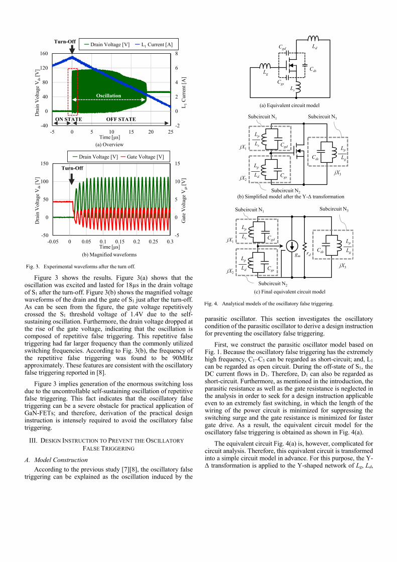
Figure 3 shows the results. Figure 3(a) shows that the oscillation was excited and lasted for 18µs in the drain voltage of S1 after the turn-off. Figure 3(b) shows the magnified voltage waveforms of the drain and the gate of S1 just after the turn-off. As can be seen from the figure, the gate voltage repetitively crossed the S1 threshold voltage of 1.4V due to the self-sustaining oscillation. Furthermore, the drain voltage dropped at the rise of the gate voltage, indicating that the oscillation is composed of repetitive false triggering. This repetitive false triggering had far larger frequency than the commonly utilized switching frequencies. According to Fig. 3(b), the frequency of the repetitive false triggering was found to be 90MHz approximately. These features are consistent with the oscillatory false triggering reported in [8].
Figure 3 implies generation of the enormous switching loss due to the uncontrollable self-sustaining oscillation of repetitive false triggering. This fact indicates that the oscillatory false triggering can be a severe obstacle for practical application of GaN-FETs; and therefore, derivation of the practical design instruction is intensely required to avoid the oscillatory false triggering.
III. DESIGN INSTRUCTION TO PREVENT THE OSCILLATORY
FALSE TRIGGERING
A. Model Construction According to the previous study [7][8], the oscillatory false
triggering can be explained as the oscillation induced by the
parasitic oscillator. This section investigates the oscillatory condition of the parasitic oscillator to derive a design instruction for preventing the oscillatory false triggering.
First, we construct the parasitic oscillator model based on Fig. 1. Because the oscillatory false triggering has the extremely high frequency, C1–C3 can be regarded as short-circuit; and, L1 can be regarded as open circuit. During the off-state of S1, the DC current flows in D1. Therefore, D1 can also be regarded as short-circuit. Furthermore, as mentioned in the introduction, the parasitic resistance as well as the gate resistance is neglected in the analysis in order to seek for a design instruction applicable even to an extremely fast switching, in which the length of the wiring of the power circuit is minimized for suppressing the switching surge and the gate resistance is minimized for faster gate drive. As a result, the equivalent circuit model for the oscillatory false triggering is obtained as shown in Fig. 4(a).
The equivalent circuit Fig. 4(a) is, however, complicated for circuit analysis. Therefore, this equivalent circuit is transformed into a simple circuit model in advance. For this purpose, the Y-Δ transformation is applied to the Y-shaped network of Lg, Ld,
Experimental waveforms after the turn off.
-2
0
2
4
6
8
-40
0
40
80
120
160
-5 0 5 10 15 20 25
L1
Cur
rent
[A
]
Time [μs]
Dra
in V
olta
ge V
ds[V
]
OFF STATEON STATE
Turn-Off
Oscillation
ー Drain Voltage [V] ー L1 Current [A]
(a) Overview
-5
0
5
10
15
-50
0
50
100
150
-0.05 0 0.05 0.1 0.15 0.2 0.25 0.3
Gat
e V
olta
ge V
gs[V
]
Time [μs]
Dra
in V
olta
ge V
ds[V
]
Turn-Off
ー Drain Voltage [V] ー Gate Voltage [V]
(b) Magnified waveforms
Analytical models of the oscillatory false triggering.
(a) Equivalent circuit model
(b) Simplified model after the Y-Δ transformation
Cgd
Cgs
Cds
Ld
Ls
Lg
jX1
jX2
jX3
Subcircuit N1 Subcircuit N3
Subcircuit N2
Cgd
Cgs
Cds
Ls
Lp
Ld
Lp
Lg
Lp
(c) Final equivalent circuit model
jX1
jX2
jX3
Subcircuit N1Subcircuit N3
Subcircuit N2
Cgd
Cgs
Cds
Ls
Lp
Ld
Lp
Lg
Lp
gmrd

and Ls in Fig. 4(a). As a result, we obtain Fig. 4(b). Inductance Lp in Fig. 4(b) is defined as
.sddggsp LLLLLLL ++= (1)
Finally, switching device S1 is modeled for the analysis. Generally, the electrical characteristics of the switching devices are highly non-linear. However, we model S1 by a simple linear model with a voltage-controlled current source and the drain-source resistance. As we have seen in the previous section, the oscillation in the gate voltage waveform in Fig. 3 has the same frequency as that in the drain voltage waveform. Therefore, it seems to be natural to suppose that the oscillatory false triggering can be modeled by a linear model, similarly as in [8]. As a result, we obtain the final equivalent circuit shown in Fig. 4(c). The mutual conductance of the voltage-controlled current source and the resistance of the drain-source resistance are denoted as gm and rd, respectively.
B. Analysis of the Oscillatory Condition Next, Fig. 4(c) is analyzed to investigate the oscillatory
condition. Note that Fig. 4(c) has a form of a Barkhausen-type oscillator. The oscillatory condition of Fig. 4(c) can be easily obtained using the Barkhausen criterion [19]. According to this criterion, the oscillation occurs, if the real part of the open-loop gain H is greater than the unity, i.e. Re(H)≥1 at the frequency at which the imaginary part of H is zero, i.e. Im(H)=0. If the reactance of subcircuits N1–N3 are denoted as X1–X3, respectively, the open-loop gain H of Fig. 4(c) is obtained as
( )
( ) ( ) .
////
321321
32
21
2321
XXXrXXXjXXrjg
XXX
jXXXjrgH
d
dm
dm
++++−=
++−=
(2)
Therefore, the open-loop gain H meets the Barkhausen criterion, if the following relations are satisfied:
,0321 =++ XXX (3)
.121
2 ≥+
−XXXrg dm (4)
The first relation, i.e. (3), is called as the frequency condition, whereas the latter, i.e. (4), is called as the gain condition.
Commonly, gmrd of switching devices tends to take a large value. Hence, we assume that gmrd is infinitely large positive value in order to simplify the discussion. In addition, we also assume that |X1| is far greater than |X2| because Cgd is commonly far smaller than Cgs and Lp/Ls is commonly far greater than Lp/Ld. Under these assumptions, the frequency and gain conditions can be reduced into a simpler equivalent condition. As a result, the Barkhausen criterion can be reduced into the following condition: At the frequency at which X1+X2+X3=0, the polarity of X1, X2, and X3 should satisfy either
1. X2 and X3 are both positive and X1 is negative; or,
2. X2 and X3 are both negative and X1 is positive.
Note that subcircuits N1–N3 are parallel-connected LC resonators in Fig. 4(c). Therefore, the polarity of their reactance is positive, if the frequency is below the resonance frequency; and the polarity is negative, if the frequency is above the resonance frequency.
Let f1–f3 be the resonance frequencies of N1–N3, respectively. Then, we can find 6 possible magnitude relations among f1–f3 as illustrated in Fig. 5. This figure indicates that only the following two relations can avoid the aforementioned condition on the polarity of X1, X2, and X3 at any frequency region:
Relation between the frequency region of the oscillation and the order of resonance frequencies f1–f3. The vertical axis is the impedance of subcircuits N1–
N3; and the horizontal axis is the frequency.
log f [Hz]
log|
X|[Ω
] Region of oscillation
N1 N3 N2
f1 f3 f2
Impe
danc
e
Frequency
(f) f1 < f3 < f2
log f [Hz]
log|
X|[Ω
]
No oscillation
N3 N1 N2
f3 f1 f2
Impe
danc
e
Frequency(b) f3 < f1 < f2
log f [Hz]
log|
X|[Ω
] Region of oscillation
N2 N3 N1
f2 f3 f1
Impe
danc
e
Frequency(c) f2 < f3 < f1
log f [Hz]
log|
X|[Ω
] Region of oscillation
N1 N2 N3
f1 f2 f3
Impe
danc
e
Frequency
(e) f1 < f2 < f3
log f [Hz]
log|
X|[Ω
]
No oscillation
N2 N1 N3
f2 f1 f3
Impe
danc
e
Frequency
(a) f2 < f1 < f3
log f [Hz]
log|
X|[Ω
] Region of oscillation
N3 N2 N1
f3 f2 f1
Impe
danc
e
Frequency
(d) f3 < f2 < f1

., 213312 ffffff <<<< (5)
Therefore, the Barkhausen criterion is not satisfied under (5); and therefore, the oscillation does not occur.
As for the other cases, i.e. f2<f3<f1, f3<f2<f1, f1<f2<f3, and f1<f3<f2, there exists a frequency region that satisfies the aforementioned condition on the polarity of X1, X2, and X3. (This frequency region is shadowed in Fig. 5.) Note that X1+X3 takes an extremely large negative value at the lowest frequency of the shadowed region, whereas X1+X3 takes an extremely large positive value at the highest frequency of the shadowed region. Therefore, there exists a frequency within the shadowed region at which X1+X2+X3 takes zero. As a result, the oscillation occurs in all the cases of f2<f3<f1, f3<f2<f1, f1<f2<f3, and f1<f3<f2.
To summarize, the occurrence of the oscillation, i.e. the oscillatory false triggering, can be avoided, if f1–f3 are designed to satisfy (5). Noting that f1–f3 are defined as the resonance frequencies of subcircuits N1–N3, we can express these frequencies as
.
2
1
,2
1,
2
1
3
21
gdsp
dgspsgdp
LCLf
LCLf
LCLf
π=
π=
π=
(6)
Substituting (6) into (5), we finally obtain the condition of the parasitic inductance for preventing the oscillatory false triggering as
.orgs
d
gd
s
ds
g
ds
g
gd
s
gs
d
CL
CL
CL
CL
CL
CL <<<< (7)
This result indicates that the oscillatory false triggering can be prevented by designing Ls/Cgd within an appropriate range of value. This fact leads to a striking idea that too small Ls, as well as too large Ls, can cause the oscillatory false triggering. Consequently, this results suggests a novel design instruction that appropriate balance between Ls and Cgd, i.e. appropriate ratio of Ls and Cgd, should be designed to satisfy (7) in order to prevent the oscillatory false triggering.
Compared with the conventional design instruction presented in [8], this design instruction can be valid even if the frequency of the parasitic resonance of the gating circuit is close to that of the power circuit. According to the analysis of [8], the frequency of the parasitic resonance of the gate circuit (fg) and the frequency of the parasitic resonance of the drain circuit (fd) can be expressed as the following equation. (We approximate that Cgd is far smaller than Cgs and Cds.)
( ) ( ) .
2
1,
2
1
dssdd
gssgg CLL
fCLL
f+π
=+π
= (8)
Therefore, if we approximate as Lg+Ls≈Lg and Ld+Ls≈Ld, (7) can be rewritten as
.
1
4
1
4or
1
4
1
4
2222
2222
dgsds
gds
ggsds
gd
ggsds
gds
dgsds
gd
fCCC
LfCC
CfCC
CL
fCCC
π<<
π
π<<
π (9)
Equation (9) indicates that the occurrence of the oscillatory false triggering can be prevented as far as Ls is designed to satisfy (9) even if fg is close to fd. Certainly, appropriate range of value for Ls is narrow under the condition in which fg is close to fd. However, appropriate design of Ls can be a universally applicable approach for preventing the oscillatory false triggering.
It is worth noting that the analysis of this section is targeted on the worst case, in which gmrd is regarded to be infinitely large and the parasitic resistance, as well as the gate resistance, is regarded to be zero. Therefore, this design instruction can cover extremely high speed switching.
Certainly, actual power converters commonly contains parasitic resistance of the wiring as well as the gate resistance. Furthermore, the actual switching devices have finite gmrd. As a result, the Q factors of subcircuits N1–N3 are finite to damp the oscillation in actual power converters. In addition, the oscillatory condition (4) become more difficult to be satisfied under finite gmrd. As a consequence, the oscillatory false triggering may occur more rarely in actual power converters and the oscillatory false triggering may be prevented for wider range of Ls.
According to our discussion, we can also say that too small Cgd is not appropriate as well as too large Cgd. From the viewpoint of the oscillatory false triggering, Cgd should be designed to have appropriate range of value. However, this does not necessarily means that the effort to minimize Cgd is meaningless. As widely known, large Cgd may deteriorate the switching speed or cause the self-turn-on. Therefore, our design instruction, shown in (7), should be interpret that reduction only in Cgd or only Ls may be harmful and that both Cgd and Ls should be reduced to keep Ls/Cgd within an appropriate range of value.
IV. EXPERIMENT
An experiment was carried out to verify the effectiveness of the proposed design instruction, i.e. suppression of the occurrence of the oscillatory false triggering by designing the appropriate balance between Cgd and Ls. In this experiment, the experimental chopper shown in Section II was employed.
Figure 6 shows the PCB layout of this experimental chopper. This chopper is designed to be able to change the value of Ls by elongating or shortening the common source path, i.e. the AC current path shared by Pg and Pd. (Pg and Pd are the AC current paths of the gating circuit and the power circuit, respectively, defined in Fig. 1.) The common source path was changed by making a solder bridge on a selected point to connect the ground of the gating circuit to the source terminal of S1. Figure 6 shows the six points for making the solder bridge to change Ls. In addition, further large Ls was implemented by cutting a part of the wiring path along the green line shown in Fig. 6. As a result, we obtained eight levels for Ls, and the range of Ls varied from

0.3nH to 1.9nH. The measurement method of Ls of the experimental chopper is described in the appendix.
In addition, the experimental chopper was designed to be able to change the value of Lg and Ld by elongating the gate and drain wiring using U-shaped wires. (The photograph of the U-shaped wires is shown in Fig. 7.) The length of the gate wiring was changed by selecting either attaching the 10mm U-shaped wire or making a solder bridge on the wiring path from the gate driver to the gate of S1. On the other hand, the length of the drain wiring was changed by attaching either one of two U-shaped wires on the wiring path from the drain of S1 to diode D1. Certainly, the values of Lg and Ld were significantly affected not only by the U-shaped wires but also by the value selected for Ls because selection of Ls also leads to elongating and shortening of Pd and Pg. Hence, selecting the U-shaped wire only determines the range of Lg and Ld. We measured the values of Lg and Ld at each value of Ls, as shown in Table II. The measurement method of Lg and Ld of the experimental chopper is also described in the appendix.
In order to evaluate the effectiveness of the proposed design instruction, we designed Lg and Ld in this experiment so that the preceding design instruction [8] was not satisfied. Hence, the
parasitic resonance frequency fg of the gating circuit was designed to be close to the resonant frequency fd of the power circuit, according to the definition given as (8). Then, we set Ls at various values and observed the non-occurrence condition of the oscillatory false triggering.
Pattern layout of the experimental PCB.
Photograph of the U-shaped wires.
Experimental result of occurrence of the oscillatory false triggering.
Lg was the original gate wiring made with the solder bridge and Ld was implemented with the 5mm U-shaped wire. Blue marks indicates the points where the theory predicted non-occurrence of the oscillatory false triggering.
Experimental result of occurrence of the oscillatory false triggering.
Lg and Ld were implemented with the U-shaped wires 5mm and 20mm, respectively. Blue marks indicates the points where the theory predicted non-occurrence of the oscillatory false triggering.
0
10
20
30
40
50
0 0.5 1 1.5 2
Gat
e-D
rain
Cap
acit
ance
Cgd
[pF]
Parasitic Inductance Ls [nH]
Points where the theory predicted no oscillatory false triggering
Experimental region ofno oscillatory false triggering
Fig. 3.
Fig. 10.
0
10
20
30
40
50
0 0.5 1 1.5 2
Gat
e-D
rain
Cap
acita
nce
Cgd
[pF
]
Parasitic Inductance Ls [nH]
Experimental region of no oscillatory false triggering
No false triggering Non-oscillatory false triggering× Oscillatory false triggering
Points where the theory predictedno oscillatory false triggering
TABLE II. INDUCTANCE VALUES FOR Lg AND Ld EMPLOYED IN THE EXPERIMENT
Ls [nH] 0.3 0.4 0.6 0.7 0.8 1.7 1.8 1.9
Lg [nH] Solder bridge 5.3 6.4 8.0 10.0 11.7 10.2 11.5 12.4
10mm wire 7.9 8.9 10.8 12.5 14.2 12.5 14.2 14.9
Ld [nH] 5mm wire 7.6 7.6 7.6 7.6 7.6 9.3 9.3 9.3
20mm wire 14.2 14.2 14.2 14.2 14.2 15.9 15.9 15.9

In this experiment, we also evaluated the dependency of the non-occurrence condition on Cgd. For this purpose, we evaluated the range of Ls that prevents the oscillatory false triggering at five values of Cgd: 9.2pF, 27pF, 31pF, 36pF, and 42pF. The first value is the original capacitance of S1, whereas the other values were implemented by adding a small-sized ceramic capacitor between the drain and gate terminals of S1.
Figures 8 and 9 show the evaluation result of the non-occurrence condition of the oscillatory false triggering. In these figures, the repetitive false triggering more than ten times after the turn-off was judged as the oscillatory false triggering. The false triggering less than 10 times was classified as the non-oscillatory false triggering.
In Fig. 8, a solder bridge was made on the wiring path of the gate instead of the U-shaped wire; and the 5mm U-shaped wire is implemented on the wiring path of the drain. As a result, Lg and Ld were ranged 5.3–12.4nH and 7.6–9.3nH, respectively.
On the other hand, in Fig. 9, the 10mm U-shaped wire was attached on the wiring path of the gate; and the 20mm U-shaped wire was attached on the wiring path of the drain. As a result, Lg and Ld were ranged 7.9–14.9nH and 14.2–15.9nH, respectively.
As can be seen in Fig. 8 and Fig. 9, the oscillatory false triggering was suppressed in a certain range of Ls. In addition, this range shifted toward larger inductance as Cgd takes the larger capacitance. These features were consistent with the theoretical analysis. Furthermore, the experimentally observed region of the no false triggering was found to cover the theoretically predicted points, suggesting appropriateness of the theory.
Figures 8 and 9 indicate that too small Ls resulted in the oscillatory false triggering, similarly as too large Ls. This result implies that balancing Ls and Cgd, i.e. optimizing the ratio Ls/Cgd, is essential for preventing the oscillatory false triggering rather than simply minimizing Ls.
Figure 10 shows the switching waveform when the oscillatory false triggering was suppressed by setting Ls at 0.6nH and Cgd at 31pF, respectively. (Lg and Ld were set at 8.0nH and 7.6nH, respectively.) As can be seen in the figure, not only the oscillatory false triggering but also the normal false triggering disappeared in the switching waveform, suggesting practical effectiveness of the proposed design instruction.
V. CONCLUSIONS
The oscillatory false triggering has been reported to be a possible severe risk for industrial application of GaN-FETs. This paper addressed this issue by proposing a design instruction to prevent this phenomenon. This paper analyzed the occurrence condition of the oscillatory false triggering, considering the common source inductance as well as the other parasitic inductance of the wiring. The analysis revealed that the ratio of the gate-drain capacitance and the common source inductance is the key factor to be optimized for effective prevention of the oscillatory false triggering. Particularly, this analysis suggested that too small common source inductance can be harmful similarly as too large common source inductance, which may imply the necessity to optimize the common source inductance rather than to minimize the inductance.
APPENDIX
A. Measurement Method of Common Source Inductance Ls
In this experiment, a recently proposed measurement technique [12][13] was employed for the common source inductance. Figure 11 illustrates the measurement method. We employed another PCB with the same layout pattern as the experimental chopper. On this PCB, only the GaN-FET was mounted. We attached resistor Rmesu on the wiring path from the gate driver to the gate terminal of the GaN-FET. In addition, ceramic capacitor Cmesu was attached to connect the pads for the output terminal and the ground terminal of the gate driver. Then, we applied the DC voltage to Cmesu in order to keep the GaN-FET at the on-state. Finally, we connected the signal generator between the drain and the source of the GaN-FET to supply the high frequency sinusoidal AC current and measured the AC voltage across Rmesu.
As discussed in the preceding studies [12][13], the voltage induced at Ls appears at Rmesu because the resistance of Rmesu was designed to be far higher than the impedance of Cgs and Lg at the frequency of the sinusoidal AC current. Hence, Ls can be obtained using the following equation:
,sin2
φπ ac
mesus fI
VL = (10)
where Vmesu and Iac are the effective value of the voltage across Rmesu and the AC current supplied from the signal generator,
Voltage waveforms at the turn-off when the oscillatory false
triggering is suppressed.
Circuit diagram of the measurement method of the common source
inductance.
5Vf
Cmesu
Signalgenerator
Cgs
Cds
Ld
Ls
Lg
S1
Iac
Rmesu
Cgd
1MΩ
0.1µF
Vmesu

respectively; f is the frequency of the AC current; and φ is the phase difference between the voltage across Rmesu and the AC current.
We measured Ls by supplying the AC current of 0.2Ap at nine frequencies from 2MHz to 10MHz. Then, we averaged the results to determine Ls. Other parameters related to this measurement is presented in Fig. 11.
B. Measurement Method of Parasitic Inductance Lg and Ld
The inductance Lg and Ld are measured using the simple measurement method for the parasitic inductance of the loop wiring path [8]. In this method, we employed another PCB with the same layout pattern as the experimental chopper, similarly as in the previous subsection.
For the measurement of Lg, only a small surface-mount ceramic capacitor with the capacitance of Cmg was mounted on the pads for the GaN-FET to connect the gate and source terminals. In addition, we disposed a solder bridge to connect the pads of the output and ground terminals of the gate driver. As a result, the capacitor was short-circuited through the wiring of the gating circuit.
Then, we measured the frequency dependence of the impedance of this short-circuited capacitor. This short-circuited capacitor forms a parallel-connected LC resonator composed of the ceramic capacitor and the parasitic inductance Lg+Ls. Therefore, the resonance frequency can be measured based on the frequency of the peak impedance. If we denote the resonance frequency as fres, Lg can be obtained as
.4
122 s
mgresg L
CfL −
π= (11)
Similarly, for the measurement of Ld, we mounted a small surface-mount ceramic capacitor with the capacitance of Cmd on the pads for the GaN-FET to connect the drain and source terminals. Then, we made solder bridges to connect the pads for diode D1 and the pads for output capacitor C3. As a result, the ceramic capacitor was short-circuited through the wiring of the power circuit. This short-circuited capacitor forms a parallel-connected LC resonator composed of the ceramic capacitor and the parasitic inductance Ld+Ls. Hence, by determining the resonance frequency as a result of the impedance measurement, we can obtain Ld as
.4
122 s
mdresd L
CfL −
π= (12)
In this experiment, we set both Cmg and Cmd at 0.22uF.
REFERENCES [1] M. A. Khan, G. Simin, S. G. Pytel A. Monti, E. Santi, and J. L. Hudgin,
“New developments in gallium nitride and the impact on power electronics,” in Proc. IEEE Power Electron. Specialist Conf. (PESC2005), 2005, pp.15-26.
[2] B. Wang, N. Tipirneni, M. Riva, A. Monti, G. Simin, and E. Santi, “An efficient high frequency drive circuit for GaN power HFETs,” IEEE Trans. Ind. Appl., Vol. 45, No.2, pp.843-853, 2009.
[3] A. Nishigaki, H. Umegami, F. Hattori, W. Martinez, M. Yamamoto, “An analysis of false turn-on mechanism on power devices,” in Proc. IEEE
Energy Conversion Congr. Expo. (ECCE2014), Pittsburgh, PA, 2014, pp. 2988–2993.
[4] H. Ishibashi, A. Nishigaki, H. Umegami, W. Martinez, and M. Yamamoto, “An analysis of false turn-on mechanism on high-frequency power devices,” in Proc. IEEE Energy Conversion Congr. Expo. (ECCE2015), 2015, pp. 2247–2253.
[5] R. Xie, H. Wang, G. Tang, X. Yang, and K. J. Chen, “An analytical model for false turn-on evaluation of high-voltage enhancement-mode gan transistor in bridge-leg configuration,” IEEE Trans. Power Electron., vol. 32, no. 8, pp. 6416–6433, Oct. 2016.
[6] K. Murata and K. Harada, “A self turn-on mechanism of the synchronous rectifier in a DC/DC converter,” in Proc. IEEE Telecommunications Energy Conf. (INTELEC2004), 2004, pp.642-646.
[7] A. Lemmon, M. Mazzola, J. Gafford, and C. Parker, “Instability in half-bridge circuits switched with wide band-gap transistors,” IEEE Trans. Power Electron., vol. 29, no. 5, pp. 2380–2392, May 2014.
[8] K. Umetani, K. Yagyu, and E. Hiraki, “A design guideline of parasitic inductance for preventing oscillatory false triggering of fast switching GaN-FET,” IEEJ Trans. Elect. Electron. Eng., vol. 11, no. S2, pp. S84–S90, Dec. 2016.
[9] W. Zhang, Z. Zhang, F. Wang, D. Costinett, L. Tolbert, and B. Blalock, “Common source inductance introduced self-turn-on in MOSFET turn-off transient,” in Proc. IEEE Appl. Power Electron. Conf. Expo. (APEC2017), 2017, pp. 837–842.
[10] B. Wang, R. Chen, and D. Jauregu, “Common source inductance (CSI) of power devices and the impacts on synchronous buck converters,” in Proc. Appl. Power Electron. Conf. Expo. (APEC2014), 2014, pp. 157–162.
[11] Z. Dong, X. Wu, K. Sheng, J. Zhang, “Impact of common source inductance on switching loss of SiC MOSFET, ” in Proc. IEEE Intl. Future Energy Electron. Conf. (IFEEC2015), 2015, pp. 1–5.
[12] K. Umetani, K. Aikawa, and E. Hiraki, “Straightforward measurement method of common source inductance for fast switching semiconductor devices mounted on-board,” IEEE Trans. Ind. Electron. (in press)
[13] K. Aikawa, T. Shiida, R. Matsumoto, K. Umetani, and E. Hiraki, “Measurement of the common source inductance of typical switching device packages,” in Proc. IEEE Intl. Future Energy Electron. Conf. (IFEEC2017), 2017, pp. 1–6.
[14] H. Umegami and A. Nishigaki, F. Hattori, and M. Yamamoto, “Investigation of false triggering mechanism,” IEEJ Trans. Elect. Electron. Eng., Vol. 9, No.1, pp. 102-104, 2014.
[15] J. Wang and H. S.-H. Chung, “Impact of parasitic elements on the spurious triggering pulse in synchronous buck converter,” IEEE Trans. Power Electron., vol. 29, no. 12, pp. 6672-6685, Dec. 2014.
[16] S. Guo, L. Zhang, Y. Lei, X. Li, W. Yu, A. Q. Huang, “Design and application of a 1200V ultra-fast integrated silicon carbide MOSFET module,” in Proc. Appl. Power Electron. Conf. Expo. (APEC2016)., 2016, pp. 2063–2070.
[17] EPC Corporation, “eGaN-FET Drivers and Layout Considerations”, White Paper WP008, 2012.
[18] Texas Instruments, “LM5113 datasheet,” pp.12, 2013.
[19] M. K. Kazimierczuk, “RF power amplifiers,” Wiley, pp. 543-545, 2015.