optical properties of ga 1-x mn x as c. c. chang, t. s. lee, and y. h. chang department of physics,...
TRANSCRIPT

Optical Properties of Ga1-xMnxAs
C. C. Chang, T. S. Lee, and Y. H. ChangDepartment of Physics, National Taiwan University
Y. T. Liu and Y. S. Huang Department of Electronics, National Taiwan University of Science and Technology
J. Furdyna
Department of Physics, University of Notre Dame

Outlines:
• Review on semiconductor spintroincs
• Basic properties of III-Mn-V
• Optical properties of GaMnAs
• Experimental results and discussions
• Summary

Review on semiconductor spintroincs
• Classical device: use the electrical and particle properties of the electron.
• Quantum device: use the wave properties of electron.
• Spin-properties- non volatile memory, integration of memory and logic devices, spin-FET, quantum computing, etc.

Requirement for spintronic devices
• 1. spin-injection• 2. spin-manipulation• 3.spin-detection• An example: spin-
FET

Problem with the spin-injection
• Conductance mismatch

Basic knowledge about magnetism
• Paramagnetism: • Atoms have magnetic moments bu
t the coupling between the magnetic moments is small and the magnetic moment of the atoms are randomly oriented.

Origin of ferromagnetism
• Direct exchange interaction
• Super-exchange interaction
• Indirect exchange

Nature Choice for magnetic semiconductor II1-x-Mnx-VI (Diluted magnetic
semiconductor)• 1. Anti-ferromagnetic at high x,
paramagnetic at low x.• 2. large spin g-factor• 3. Spin polarized LED, Spin su
perlattice, etc.

MBE phase diagram of Ga1-xMnxAs

Some basic knowledge about the material properties of Ga1-xMnxAs
• The samples were grown at low temperature with MBE, the quality of the material is usually very poor
• Mn is an acceptor and in principle could donate a hole for electrical conduction.
• Mn in GaMnAs is a substitutional acceptor? (yes, Soo et al. APL 80, 2654 (2002)
• Metal-insulator transition and Anderson localization are essential ingredient of the problem
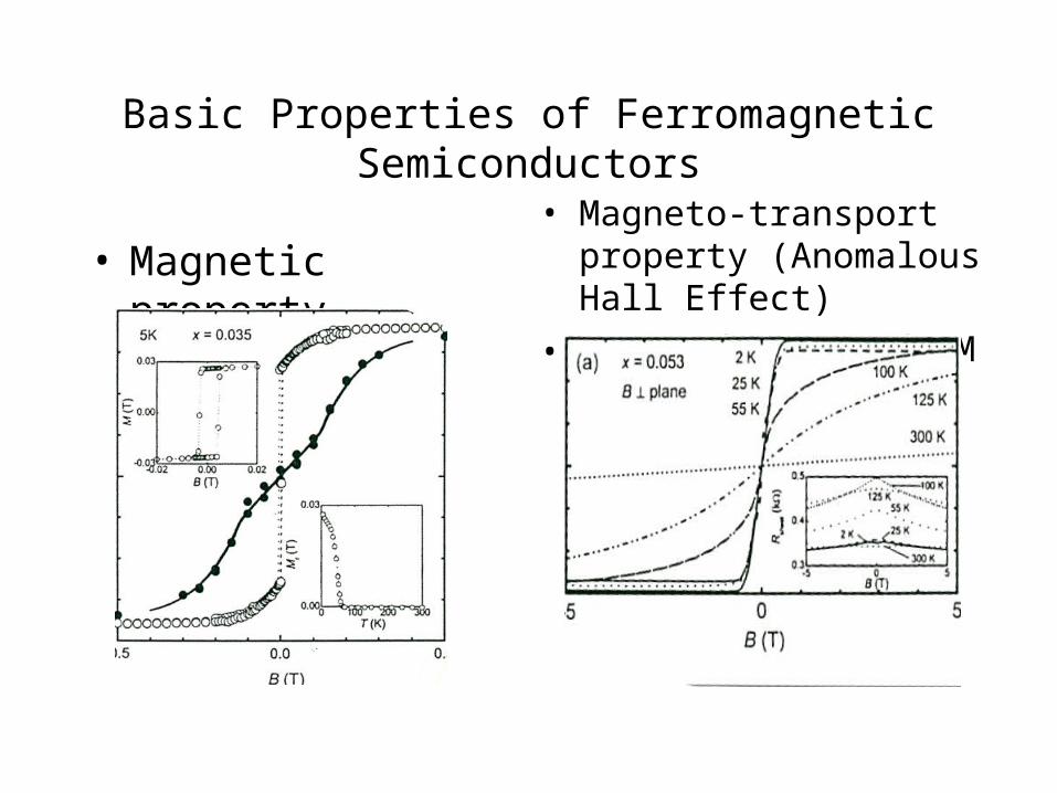
Basic Properties of Ferromagnetic Semiconductors
• Magnetic property• Magneto-transport
property (Anomalous Hall Effect)
• RH=(R0/d) B+(RM/d) M

Carrier induced ferromagnetism?
• Dependence of TC on x Metal-insulator transitions

Summary of optical studies
• InMnAs (Hirakawa et al.,, Physica E10, 215 (2001))
• The conductivity could be well fitted with Drude model, indicating the holes are delocalizd.
• Localization length of hole estimated to be 3-4 nm, close to the average inter-Mn distance.
• Add figure from their paper

• GaMnAs:(Hirakawa et al. PRB 65, 193312, (2002))
• Non-Drude-like FIR response observed.
• Broad conductivity peak near 200meV observed.
• Estimated mean free path of 0.5nm implies that even for the metallic sample the hole wavefunction is localized. RKKY?

• GaMnAs (Singley et al. PRL 89, 097203 (2002))
• A broad band centered at 200 meV is observed.
• From the sum rule analysis it was found that the charge carrier has a very heavy effective mass 0.7me< m*< 15me. for the x=.052 sample. It is suggested that the holes reside in the impurity band

• GAMnAs (Yang et al., PRB 67, 04505 (2003))
• A non-perturbative self-consistent study which treat both disorder and interaction on equal footing.
• The broad peak centered at 220 meV is present even in a one band approximation.
• Non-Drude behavior could be accounted for if multiple scattering is taken in to consideration
• A new feature at around 7000 cm-1, originated from the transition from heavy hole to split off band is predicted.

Meatal-insulator transitions in doped semiconductor
• Impurity level broaden into an impurity band.
• Impurity band merge with the valence band.
• Where are position of the Fermi level and the position of the mobility edge?

Samples:
Sample Mn concentration Structure
(Bottom>Top)
Growth time Thickness
10529A X=1.4% GaAs
LT-GaAs
LT-GaMnAs
8 min
8 min
24 min
100 nm
100 nm
300 nm
01016A X=2.4% GaAs
LT-GaAs
LT-GaMnAs
8 min
8 min
24 min
100 nm
100 nm
300 nm
30422A X=3.3% GaAs
LT-GaAs
LT-GaMnAs
30min
11sec
800 sec
400 nm
2nm
200 nm
11127A X=4.8% GaAs
LT-GaAs
LT-GaMnAs
30min
11sec
900 sec
400 nm
2 nm
210 nm
21028G X=6.2% GaAs
LT-GaAs
LT-GaMnAs
20min
12sec
500 sec
300 nm
2.6 nm
120nm

T-dependent magnetization

T-dependent RXX

• Source Beam splitter Detector • NIR (13000~4000 cm-1) Tungsten Si/Ca InSb (LN2) • MIR(4000~400 cm-1) Globar KBr MCT (LN2) • FIR(400~10 cm-1) Hg Lamp Mylar 6μm Bolometer (LHe)

FIR transmission data
• Flat response in the low energy region
• Zero transmission for x=4.8% sample
0 50 100 150 200 250 300 350 4000.0
0.2
0.4
0.6
0.8
T=300 K
Ga1-x
MnxAs
Tra
ns
mit
tan
ce
(a
.u.)
Frequency (cm-1)
x=1.4%x=2.4%x=3.3%x=4.8%

Transmission data –IR and near IR
0 2000 4000 6000 8000 10000 120000.0
0.2
0.4
0.6
0.8
1.0
1.2
T=300 K
Ga1-x
MnxAs
T
ra
ns
mit
tan
ce
(a
.u.)
Frequency (cm-1)
x=1.4%x=2.4%x=3.3%x=4.8%
Absorption dips for low x samp[learound 2000 cm -1.
Peculiar behavior of x=4.8% sample: below opaque below about 1500cm-1 but become transparent above 1500 cm-1

Plasma frquency
• ωp=(4πn e2/ m*) ½
• n=m* ωp2 / 4πn e2
• Take ћ ωp= 2000cm-1, m*= 0.5 me, we get
• n=5* 10 19 cm-3
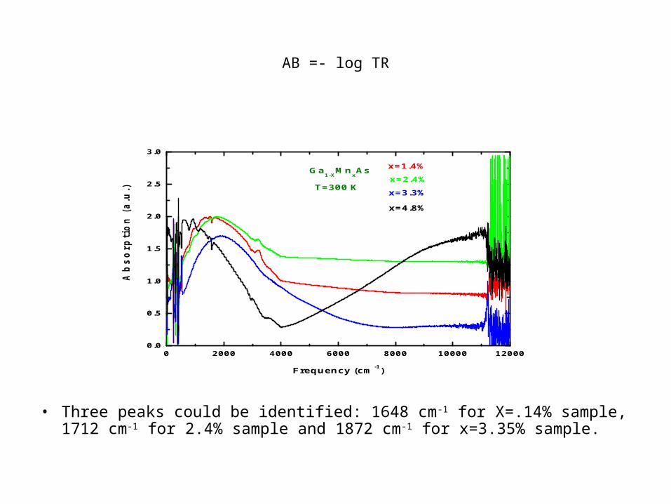
AB =- log TR
0 2000 4000 6000 8000 10000 120000.0
0.5
1.0
1.5
2.0
2.5
3.0
x=4.8%
x=3.3%
x=2.4%
x=1.4%
A
bs
orp
tio
n (
a.u
.)
Frequency (cm-1)
Ga1-X
MnxAs
T=300 K
• Three peaks could be identified: 1648 cm-1 for X=.14% sample, 1712 cm-1 for 2.4% sample and 1872 cm-1 for x=3.35% sample.

Absorption spectra in mid and near IR
4000 6000 8000 100000.0
0.5
1.0
1.5
2.0
x=4.8%
x=3.3%
x=2.4%
x=1.4%
A
bs
orp
tio
n (
a.u
.)
Frequency (cm-1)
Ga1-X
MnxAs
T=300 K

Refletance spectra in FIR
0 50 100 150 200 250 300 350 4000.0
0.5
1.0
1.5
2.0
2.5
3.0
Re
fle
cta
nc
e (
a.u
.)
Frequency (cm-1)
x=2.4%
x=4.8%x=3.3%
x=1.4%GaxMn
1-xAs
T=300 K

Reflectance spectra in mid-IR and near IR
0 2000 4000 6000 8000 10000 120000.0
0.5
1.0
1.5
2.0
R
efl
ec
tan
ce
(a
.u.)
Frequency (cm-1)
x=2.4%
x=4.8%x=3.3%
x=1.4%Ga1-x
MnxAs
T=300 K

Real part of conductivity in the mid and near IR
0 2000 4000 6000 8000 10000 120000.0
2.0x10²
4.0x10²
6.0x10²
8.0x10²
σ
1(ω
)(Ω-1
m-1)
Wave Number (cm-1)
x=1.4% x=2.4% x=3.3%
GaxMn
1-xAs
T=300K

4000 6000 8000 100000.0
2.0x10²
4.0x10²
σ1(ω
)(Ω-1
m-1
)
Wave Number (cm-1)
x=1.4% x=2.4% x=3.3%
GaxMn
1-xAs
T=300K

CER Measurement System圖四
MotorDriver
PC
Monochromator
Black Box
Detector
Focus Lens
GPIB
Light Source
VNDF
Lock-inAmplifier
Signals in
Ref.out
PowerSupply
Focus Lens
High VoltageAmplifier Input
Voltage Monitor
Input
OscilloScope
Sample
High Voltage output
Long PassFilter

Band filling effect for InP heavily doped with Se
• P.M. Raccah et al., APL 39, 496 (1981)
• High doping concentration > 10 20 cm-1
• Optical gap increases from 1.34 to 1.9 eV

Contactless electro-reflectance (CER) results
1.35 1.40 1.45 1.50 1.55 1.60 1.65
R/R
Photon Energy (eV)
15K 30K 50K 77K X 1.5 100K X 2 125K X 2 150K X 3 175K X 4 200K X 5 225K X 5.8 250K X 7 275K X 18 300K X 24
01016A CER Mn=2.4%

1.30 1.35 1.40 1.45 1.50 1.55 1.60 1.65
11127A CER Mn=4.8% R
/R
Photon Energy (eV)
15K 30K 50K 77K 100K 125K X 1.5 150K X 2 175K X 3 200K X 4 225K X 8 250K X 15 275K X 25 300K X 13

0 50 100 150 200 250 300
1.40
1.42
1.44
1.46
1.48
1.50
1.52
En
erg
y (
eV
)
Temperature (K)
Band gap VS Temperature
X=1.4% X=2.4% X=3.3% X=4.8% X=6.2%

Above bandgap feature in the CER spectra: band filling effect?
1.3 1.4 1.5 1.6 1.7 1.8-0.0006
-0.0004
-0.0002
0.0000
0.0002
0.0004
0.0006
0.000810529A CER 30K Mn=1.4%
R/R
Photon Energy (eV)
X 3
1.40 1.45 1.50 1.55 1.60 1.65-0.006
-0.004
-0.002
0.000
0.002
0.004
1.546 eV
R/R
Photon Energy (eV)
30422A CER 30K Mn=3.3%
X 20
1.40 1.45 1.50 1.55 1.60 1.65-0.0008
-0.0006
-0.0004
-0.0002
0.0000
0.0002
0.0004
1.5394 eV
11127A CER 30K Mn=4.8%
R/R
Photon Energy (eV)
1.40 1.45 1.50 1.55 1.60 1.65 1.70
-0.0020
-0.0015
-0.0010
-0.0005
0.0000
0.0005
0.0010
0.0015
0.0020 21028G CER 30K Mn=6.2%
1.532 eV
X 6
R/R
Photon Energy (eV)
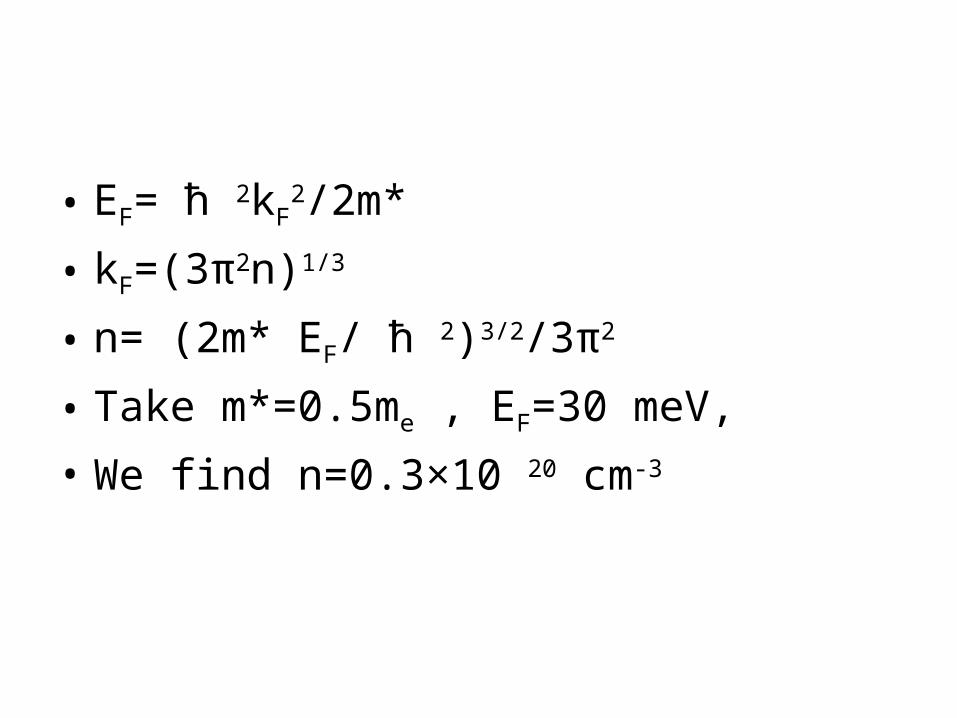
• EF= ћ 2kF2/2m*
• kF=(3π2n)1/3
• n= (2m* EF/ ћ 2)3/2/3π2
• Take m*=0.5me , EF=30 meV,
• We find n=0.3×10 20 cm-3

Summary and Conclusions:
• The FIR response of the sample appears to be flat• Non-Drude-like optical conductivity behavior is observed in the mid-I
R spectra• Clear Absorption peaks observed for sample with x<=3.3%• Metallic behavior obseved for samples with x>=4.8%• From the the transmission data, plasma frequency and carrier conce
ntration could be obtained. • Indication of band filling effect observed for some samples with EF a
bout 30 meV high than the valence band edge. • The carrier concentration obtained from plasma frequency are consi
stent with the carrier concentration obtained from the band filling effect.