optical performance monitoring in optical packet … · optical performance monitoring in optical...
TRANSCRIPT

Departamento de Comunicaciones
Universidad Politécnica de Valencia
Thesis for the degree of Doctor of Philosophy
Optical performance monitoring in
optical packet-switched networks
Ruth Vilar Mateo
Supervisor:
Dr. Francisco Ramos Pascual
Valencia, 2010


Acknowledgments
The work presented in this Thesis was conducted with the kind help and support of many people to whom I would like to express my more sincere gratefulness.
Firstly, I wish to thank Prof. Javier Martí who gave me the opportunity to become a member of his research group.
Also, I would like to thank my supervisor, Prof. Francisco Ramos, for his ongoing support and helpful advises in conducting and completing this work. Thank you for all the time you devoted to me.
Many thanks also go to all the members of the NTC group for being always willing to help and create such friendly environment, making my time there more enjoyable. I wish you all the best.
Moreover, I want to thank Prof. Sophie LaRochelle from Université Laval (Quebec, Canada), Prof. Ampalavanapillai Nirmalathas and Dr. Nishaan Nadarajah from NICTA Victoria Research Laboratory (Melbourne, Australia), and Prof. António Teixeira from Instituto de Telecomunicaçoes (Aveiro, Portugal) who took care of me during my internships in the corresponding institutes.
I feel grateful for the financial support I have received from the Spanish Government through my FPU grant.
Finally, I can never thank enough my beloved family for their love and unconditional support in all aspects of my life. And last but not least, I wish to thank my “sun”, Jaime, who has always supported me throughout this adventure. It is your love that makes my life beautiful.


Table of contents
Resumen ................................................................................................................i
Resum................................................................................................................... iii
Abstract..................................................................................................................v
List of acronyms................................................................................................... vii
Chapter 1. Introduction ...................................................................1
1.1. Rationale........................................................................................................ 1 1.2. Framework of this Thesis .............................................................................. 3 1.3. Research objectives ...................................................................................... 4 1.4. Outline of this work ........................................................................................ 5 1.5. Contributions of this Thesis ........................................................................... 7 1.6. References .................................................................................................... 9
Chapter 2. Evolution from OCS to OPS networks....................... 11
2.1. Introduction .................................................................................................. 11 2.2. Optical network evolution ............................................................................ 12 2.3. Optical packet switched networks ............................................................... 18 2.4. All-optical label switching (AOLS): the LASAGNE project........................... 20 2.5. Migration scenarios: State of the art............................................................ 26 2.6. Proposed migration scenarios in LASAGNE project ................................... 28
2.6.1. Introduction of OPS nodes in an OCS network .................................... 28 2.6.1.1 Node per node migration ................................................................ 29

2.6.1.2. Migration based on the definition of OPS node islands:................ 30 2.6.2. Client-Server hybrid optical network..................................................... 32 2.6.3. ORION .................................................................................................. 33
2.7. LASAGNE node modification: Performance monitoring and recovery issues............................................................................................................................ 36
2.7.1. Routing protocol based on quality requirements .................................. 41 2.8. Summary and conclusions .......................................................................... 43 2.9. References .................................................................................................. 46
Chapter 3. Optical performance monitoring in optical networks. State of the art................................................................................51
3.1. Introduction .................................................................................................. 51 3.2. Optical performance monitoring .................................................................. 52 3.3. Current OPM technologies for transparent circuit switched networks......... 56
3.3.1. Optical Spectrum Analyzer (OSA) ........................................................ 57 3.3.2. Polarization nulling ............................................................................... 57
3.4. Advanced OPM concepts for dynamically reconfigurable networks ........... 58 3.4.1. RF spectrum analysis ........................................................................... 59
3.4.1.1. Pilot tones ...................................................................................... 59 3.4.1.2. Clock tones .................................................................................... 62
3.4.2. Sampling methods................................................................................ 63 3.4.3. Monitoring based on interferometric configurations ............................. 65
3.4.3.1. Chromatic dispersion monitoring using an optical delay-and-add filter ............................................................................................................. 65 3.4.3.2. OSNR monitoring method based on optical delay interferometer. 66 3.4.3.3. Simultaneous monitoring of chromatic and polarization-mode dispersion in OOK and DPSK transmission ............................................... 67
3.4.4. Polarization-based methods ................................................................. 67 3.4.4.1. Monitoring based on degree-of-polarization (DOP) measurements.................................................................................................................... 67 3.4.4.2. Monitoring using polarization scrambling ...................................... 69 3.4.4.3. OSNR monitoring technique based on the orthogonal delayed-homodyne method ...................................................................................... 70
3.4.5. Nonlinear effects................................................................................... 71 3.4.5.1. OPM using nonlinear detection ..................................................... 71 3.4.5.2. Monitoring techniques based on Four-Wave Mixing ..................... 72 3.4.5.3. Monitoring techniques based on SPM and/or XPM....................... 73
3.4.6. Comparison of existing monitoring techniques..................................... 75 3.5. OPM in optical packet-switched networks................................................... 77
3.5.1. All-optical Time-to-Live using error-checking labels in optical label switching networks.......................................................................................... 78 3.5.2. An OSNR monitor for optical packet switched networks ...................... 79 3.5.3. Single technique for simultaneous monitoring of OSNR and chromatic dispersion at 40 Gbit/s .................................................................................... 80

3.5.4. Basis of monitoring techniques proposed in this Thesis ...................... 81 3.5.4.1. Monitoring-field/payload separation circuit. ................................... 82 3.5.4.2. Monitoring field definition............................................................... 84
3.6. Summary and conclusions .......................................................................... 85 3.7. References .................................................................................................. 87
Chapter 4. OSNR monitoring using optical correlators..............95
4.1. Introduction .................................................................................................. 95 4.2. OSNR monitoring for OPS networks ........................................................... 96
4.2.1. Description of the OSNR monitor ......................................................... 98 4.3. FBG-based optical correlator..................................................................... 102
4.3.1. FBG-based correlator design ............................................................. 103 4.3.2. Fabrication process ............................................................................ 112 4.3.3. Characterization of the fabricated correlator ...................................... 118
4.4. Experimental validation of the OSNR monitoring technique ..................... 119 4.5. Applications of the proposed OSNR monitoring technique ....................... 124
4.5.1. Monitoring for QoS implementation .................................................... 124 4.5.2. Monitoring for OSNR-assisted routing................................................ 126 4.5.3. Path monitoring for restoration functions............................................ 128
4.6. Summary and conclusions ........................................................................ 129 4.7. References ................................................................................................ 131
Chapter 5. PMD monitoring using XOR gate ............................. 135
5.1. Introduction ................................................................................................ 135 5.2. Principle of operation................................................................................. 136
5.2.1. XOR-based DGD Monitoring .............................................................. 137 5.2.2. Optical packet switch.......................................................................... 139
5.3. Simulation results ...................................................................................... 141 5.4. Experimental validation ............................................................................. 146 5.5. Summary and conclusions ........................................................................ 150 5.6. References ................................................................................................ 154
Chapter 6. All-optical TTL decrementing using XOR gates .....157
6.1. Introduction ................................................................................................ 157 6.2. TTL-based monitoring system................................................................... 158
6.2.1. Basis of the TTL-based monitoring..................................................... 158 6.2.2. Description of the system ................................................................... 160 6.2.3. 1-bit binary subtraction ....................................................................... 161 6.2.4. Architecture of the 1-bit binary subtractor .......................................... 161

6.3. Results and discussion.............................................................................. 166 6.4. Conclusions ............................................................................................... 171 6.5. References ................................................................................................ 173
Chapter 7. PMD monitoring using RF tones.............................. 175
7.1. Introduction ................................................................................................ 175 7.2. Study of the applicability of the monitoring techniques based on RF spectrum measurement in optical packet-switched networks .......................... 177
7.2.1. Synchronization issues....................................................................... 177 7.2.2. Response time.................................................................................... 177 7.2.3. Sensitivity analysis.............................................................................. 178
7.3. DGD monitoring using an additional shifted optical carrier ....................... 180 7.3.1. Description of the DGD monitoring technique .................................... 181 7.3.2. Simulation results ............................................................................... 184 7.3.3. Modelling of the cascade of two DGD elements ................................ 187
7.4. DGD monitoring using an additional orthogonal shifted optical carrier ..... 193 7.4.1. Description of the DGD monitoring technique .................................... 193 7.4.2. Simulation results ............................................................................... 194 7.4.3. Experimental results ........................................................................... 196
7.5. Summary and conclusions ........................................................................ 201 7.6 References ................................................................................................. 203
Chapter 8. Conclusions and future work ................................... 207
8.1. Introduction ................................................................................................ 207 8.2. Summary of the work................................................................................. 207 8.3. Future work................................................................................................ 211 8.4. References ................................................................................................ 214
Appendix A. Matrix transfer approach....................................... 217
A.1. Introduction................................................................................................ 217 A.2. Transfer matrix of uniform FBG................................................................. 217 A.3. Transfer matrix of phase-shifted gratings. ................................................ 221
Appendix B. VPI simulation parameters and schematics ........ 223
B.1. Introduction................................................................................................ 223 B.2. Simulation schemes .................................................................................. 223

B.2.1. PMD monitoring using XOR gate ....................................................... 223 B.2.2. All-optical TTL decrementing using XOR gates ................................. 228
Appendix C. List of Ph.D. publications......................................231


i
Resumen
Para poder satisfacer la demanda de mayores anchos de banda y los requisitos de los nuevos servicios, se espera que se produzca una evolución de las redes ópticas hacia arquitecturas reconfigurables dinámicamente. Esta evolución subraya la importancia de ofrecer soluciones en las que la escalabilidad y la flexibilidad sean las principales directrices. De acuerdo a estas características, las redes ópticas de conmutación de paquetes (OPS) proporcionan altas capacidades de transmisión, eficiencia en ancho de banda y excelente flexibilidad, además de permitir el procesado de los paquetes directamente en la capa óptica. En este escenario, la solución all-optical label switching (AOLS) resuelve el cuello de botella impuesto por los nodos que realizan el procesado en el dominio eléctrico. A pesar de los progresos en el campo del networking óptico, las redes totalmente ópticas todavía se consideran una solución lejana. Por tanto, es importante desarrollar un escenario de migración factible y gradual desde las actuales redes ópticas basadas en la conmutación de circuitos (OCS). Uno de los objetivos de esta Tesis se centra en la propuesta de escenarios de migración basados en redes híbridas que combinan diferentes tecnologías de conmutación. Además, se analiza la arquitectura de una red OPS compuesta de nodos que incorporan nuevas funcionalidades relacionadas con labores de monitorización y esquemas de recuperación.
Las redes que realizan el procesado en el dominio óptico permiten mejorar la transparencia de la red, pero a costa de aumentar la complejidad de las tareas de gestión. En este escenario, la monitorización óptica de prestaciones (OPM) surge como una tecnología capaz de facilitar la administración de las redes OPS, en las que cada paquete sigue su propia ruta en la red y sufre un nivel diferente de degradación al llegar a su destino. Aquí reside la importancia de OPM para garantizar los requisitos de calidad de cada paquete. El segundo y principal objetivo de esta Tesis se centra en proponer nuevas técnicas de monitorización para las redes OPS, cuyas principales características serán la realización de la monitorización a nivel de paquete y trabajar directamente en el dominio óptico. Para ello, se hará uso de un campo específico de monitorización en la cabecera óptica.
Adicionalmente, también se investiga la utilización de técnicas de monitorización basadas en la combinación de la señal óptica con señales de RF para su aplicación en redes ópticas de paquetes, dando lugar a la propuesta de dos técnicas de bajo coste para la monitorización de PMD a alta velocidad.

ii

iii
Resum
A fi de satisfer les demandes de majors amples de banda i els requisits dels nous serveis, s’espera que es produeixca una evolució de les xarxes òptiques cap a arquitectures reconfigurables dinàmicament. Aquesta evolució subratlla la importància d’oferir solucions en les quals l’eficiència i la flexibilitat sigan les principals directrius. D’acord a aquestes característiques, les xarxes òptiques de conmutació de paquets (OPS) ofereixen altes capacitats de transmissió, eficiència en ample de banda i excel·lent flexibilitat, a més de permetre el processament dels paquets directament en la capa òptica. En aquest escenari, la solució all-optical label switching (AOLS) resol el coll d'ampolla imposat pels nodes que realitzen el processat en el domini elèctric. Tot i els progressos en el camp del networking òptic, les xarxes totalment òptiques encara es consideren una solució llunyana. Per tant, és important desenvolupar un escenari de migració factible i gradual des de les actuals xarxes òptiques basades en la commutació de circuits (OCS). Un dels objectius d'aquesta Tesi se centra en la proposta d’escenaris de migració basats en xarxes híbrides que combinen diferents tecnologies de commutació. A més, s’analitza l’arquitectura d’una xarxa OPS composta de nodes que incorporen noves funcionalitats relacionades amb labors de monitoratge i esquemes de recuperació.
Les xarxes que realitzen el processat en el domini òptic permeten millorar la transparència de la xarxa, però a costa d'augmentar la complexitat de les tasques de gestió. En aquest escenari, el monitoratge òptic de prestacions (OPM) es presenta com una tecnologia capaç de facilitar l'administració de les xarxes OPS, en les que cada paquet segueix el seu propi camí en la xarxa i sofreix un diferent nivell de degradació en arribar al seu destí. Ací resideix la importància d‘OPM per garantir els requisits de qualitat de cada paquet. El segon i principal objectiu d'aquesta Tesi es centra en proposar noves tècniques de monitoratge per a les xarxes OPS, on les principals característiques seran la realització del monitoratge a nivell de paquet i treballar directament en el domini òptic. Per a això, es fará us d’un camp específic de monitoratge en la capçalera òptica.
Addicionalment, també s'investiga la utilització de tècniques de monitoratge basades en la combinació de la senyal òptica amb senyals de RF per a la seua aplicació en xarxes òptiques de paquets, donant lloc a la proposta de dues tècniques de baix cost per al monitoratge de PMD a alta velocitat.

iv

v
Abstract
To meet the increasing requirements for higher bandwidth and novel services, an evolution from static optical networks to dynamically reconfigurable architectures is expected. This evolution highlights the importance of providing network solutions putting forward scalability and flexibility as most critical specifications. According to these requirements, optical packet switching (OPS) networks provide high throughput, bandwidth efficiency, and excellent flexibility, as well as offering new capabilities to process packets directly at the optical layer. At this scenario, all-optical label switching (AOLS) appears to be a solution to avoid the bottleneck imposed by the nodes based on electronic processing. Notwithstanding the progress done in the field of all-optical networking, truly all-optical networks are still considered to be a long term solution. Hence, it is of crucial importance to develop a realistic and gradual migration scenario starting from current optical circuit-switched (OCS) networks. One of the topics addressed in this Thesis focuses on the proposal of migration scenarios based on hybrid networks which combine different types of switching technologies. Moreover, the design of an all-optical packet-switched network composed of optical nodes including new functionalities directly correlated with performance monitoring and recovery schemes is investigated.
All-optical networks allow the network transparency to be improved but at the expense of increasing the complexity of the network management. In this scenario, optical performance monitoring (OPM) appears as an enabling technology for managing future OPS networks, where each packet follows its own path and will suffer a different degradation level at the destiny. So that, OPM is especially important to ensure that packets receive an appropriate treatment. The second and main topic of this Thesis focuses on the proposal of new monitoring techniques for OPS networks, where the main features will be performing the monitoring on a packet basis and directly working in the optical domain. To this end, a specific monitoring field will be inserted into the packet header.
Additionally, the use of monitoring techniques for their applicability to OPS networks based on the combination of the optical signal with RF signals is also studied, giving place to the proposal of two cost-effective PMD monitoring techniques for high data rate transmission.
.

vi

vii
List of acronyms
AOLS All-optical Label Switching
ASE Amplified Spontaneous Emission
ATM Asynchronous Transfer Mode
AWG Arrayed Waveguide Grating
BER Bit Error Rate
CD Chromatic Dispersion
CSRZ Carrier-Suppressed Return-to-Zero
CW Continuous Wave
DGD Differential Group Delay
DOP Degree of Polarization
DPSK Differential Phase-Shift Keying
DQPSK Differential Quadrature Phase-Shift Keying
DSB Dual Side Band
DWDM Dense Wavelength Division Multiplexing
EDFA Erbium-Doped Fiber Amplifier
FBG Fiber Bragg Grating
FFT Fast Fourier Transform
FWHM Full Width Half Maximum
FWM Four Wave Mixing
GMPLS Generalized MPLS
GVD Group Velocity Dispersion
HNLF Highly Nonlinear Fiber
IP Internet Protocol
LSB Lower Side Band
LSR Label Switched Router
MPLS Multi Protocol Label Switching

viii
MZ Mach-Zehnder
MZI Mach-Zehnder Interferometer
NRZ Non Return-to-Zero
OBS Optical Burst Switching
OCS Optical Circuit Switching
ODI Optical Delay Interferometer
ODL Optical Delay Line
O/E/O Optical to Electrical to Optical
OFDM Orthogonal Frequency Division Multiplexing
OLS Optical Label Switching
OOK On-Off Keying
OPM Optical Performance Monitoring
OPS Optical Packet Switching
OSA Optical Spectrum Analyzer
OSNR Optical Signal-to-Noise Ratio
OXC Optical Cross-Connect
PBS Polarization Beam Splitter
PC Polarization Controller
PD Photodiode
PDL Polarization Dependent Loss
PMD Polarization Mode Dispersion
PRBS Pseudo-Random Binary Sequence
PSP Principal State of Polarization
QoS Quality of Service
RF Radio Frequency
RFSA RF Spectrum Analyzer
RZ Return-to-Zero
SDH Signal Digital Hierarchy
SLA Service Level Agreement
SOA Semiconductor Optical Amplifier

ix
SONET Synchronous Optical Network
SOP State of Polarization
SPM Self-Phase Modulation
SRS Stimulated Raman Scattering
SSB Single Side Band
USB Upper Side Band
XGM Cross Gain Modulation
XPM Cross Phase Modulation
WDM Wavelength Division Multiplexing


1
Chapter 1
Introduction
1.1. Rationale
In the last few years, emerging services such as voice-over-IP, video streaming, high definition TV and peer-to-peer file transfer are becoming increasingly popular on top of the traditional Internet services. As a result, telecommunication networks are experiencing a dramatic increase in the demand for such real-time and dynamic bandwidth-intensive applications which is pushing the limits of existing network structure [Mor07]. To satisfy this new demand two main factors have emerged. The first factor has been the use of wavelength division multiplexing (WDM) which has dramatically increased the network capacity. The second factor has been to increase the data channel bitrate. Nowadays, 10-Gbit/s WDM networks have been deployed and systems operating at 40 Gbit/s or beyond have been experimentally demonstrated in research labs [Hof05]. However, WDM networks are relatively statics and the conventional electronic routers have not been capable of offering a cost-effective solution to the increasing bandwidth demand [Nei05].
To support this demand economically, transport networks are evolving to provide a reconfigurable optical layer, putting forward scalability and flexibility as most critical specifications. According to these new requirements, optical packet switching (OPS) provides high throughput, bandwidth efficiency, rich routing functionalities, and excellent flexibility [Jou01, Mah01, Yao01]. These characteristics make it an excellent candidate for next-generation optical networks, which will be much more dynamic and demanding than today’s networks.

Chapter 1. Introduction
2
On the other hand, OPS technology offers a new capability to process packets directly at the optical layer. At this point, all-optical label switching (AOLS), which is a type of packet switching, appears to be a solution to avoid the bottleneck imposed by the nodes based on electronic processing [Blu00]. In such an AOLS scenario, all packet-by-packet routing and forwarding functions of multiprotocol label switching (MPLS) are implemented directly in the optical domain. By using optical labels, the IP packets are directed through the core optical networks without requiring O/E/O concersions whenever a routing decision is necessary. The main advantage of this approach is the ability to route packets/bursts independently of bitrate, packet format, and packet length.
The design of a network architecture based on the AOLS scenario with all-optical packet switching nodes opens new opportunities from an operator’s viewpoint since the all-optical solution optimizes the network technologies, allowing for a generalized introduction of broadband services at affordable price. Hence, to bring AOLS to market, network operators must be convinced of the opportunities it creates to better serve their clients. At this point, all-optical networks fulfil the new requirements that different applications impose in terms of capacity, functionality, and quality of service (QoS) available to end users [Cae07].
Apart from the benefits that AOLS brings to the implementation of next-generation networks, high throughput packet nodes can play an interesting role as single multi-service and multi-client platforms, because they would enable the realization of a transport network capable of routing data belonging to different services employing different technologies in the access/metro area [Pap033].
To propose a low cost feasible scenario for optical packet-switching, it is of crucial importance to develop a realistic and gradual migration scenario starting from current optical circuit-switched (OCS) networks. Mixed circuit-packet scenarios seem to be a feasible solution to facilitate the migration towards the final OPS solution. The study of the migration scenarios from OCS networks to an AOLS network considering both networking and economical aspects as well as the implications on the node architecture are crucial to provide scalable, flexible, and user-centric future networks. In this migration, the optical networks are also moving from point-to-point networks to more efficient and flexible data-oriented solutions that, in the longer run, will lead to intelligent optical networks. The introduction of intelligence in such networks should allow to meet emerging requirements such as: dynamic and rapid provisioning of connections, automatic topology discovery and network inventory, traffic engineering, and faster optical restoration.
In addition, all-optical networks allow the network transparency to be improved but at the expense of increasing the complexity of the network management. Indeed, the quality of signals becomes more vulnerable to the optical layer impairments. For the proper operation and management of such networks, it is essential to have the capability to monitor the parameters affecting networks performances directly in the optical layer. Furthermore, the new optical layer

Chapter 1. Introduction
3
functionality including dynamic reconfiguration and optical path restoration add new challenges in the implementation of monitoring functions in the optical domain. All of these issues bring focus to optical performance monitoring (OPM) as an enabling technology for future OPS networks [Kil04]. Indeed, OPM will be helpful for carriers to provide guaranteed quality of signal transmission to their users. Specially in OPS networks, optical paths transport different types of traffic with different quality requirements so that OPM is especially important to ensure that packets receive appropriate treatment as they travel through the network. Therefore, the following questions related to performance monitoring are the special interest:
How to perform OPM on a packet basis?
How to develop a monitoring module with fast response time and wide dynamic range?
How to associate the monitored parameters with the switch controls and header information?
How to integrate the monitoring information with the control and management planes to provide some kind of network intelligence?
In this Thesis, these questions are addressed and new ways to monitor signal quality in OPS networks with the right balance between cost and performance are investigated.
In next sections, the objectives of this Thesis are presented and a quick reference to the Thesis contents is also provided.
1.2. Framework of this Thesis
This Thesis has been carried out at the Valencia Nanophotonics Technology Center from the Universidad Politecnica de Valencia inside the “Optical Networks and Systems” research area.
The work related to the design of an all-optical network architecture and the definition of migration scenarios towards OPS networks has been performed in the framework of the European Commission funded FP6 IST-LASAGNE (“All-optical label swapping employing optical logic gates in network nodes”) project, whose main goal was the design and implementation of the first, modular, scalable and truly all-optical photonic router capable of operating at 40 Gbit/s [Ram05]. LASAGNE objectives included studying, proposing, and validating the use of all-optical logic gates based on commercially available technologies to implement network functionalities at the metro/core network nodes in AOLS networks.

Chapter 1. Introduction
4
The work related to optical performance monitoring has been partially performed inside the European Commission funded Network of Excellence BONE (“Building the future optical network in Europe”) in the work package devoted to the identification of all-optical techniques which can be applied to the packets in order to help routing at router level (e.g. discard, regeneration, etc).
Furthermore, during the course of this Thesis, the author has made several internships in different research institutes listed below:
“Centre d’Optique, Photonique, et Laser (COPL)”, Université Laval, Québec, Canada in 2008. The work was supervised by Prof. Sophie LaRochelle. The aim of the internship was focused on the design, writing, and characterization of fiber Bragg gratings for quality monitoring of optical packets.
“NICTA Victoria Research Laboratory”, University of Melbourne, Australia in 2009. The work was supervised by Prof. Ampalavanapillai Nirmalathas and by Dr. Nishaan Nadarajah. The objective of this internship was focused on analysing and proposing quality signal monitoring techniques by using RF tones for photonic packet-switched networks.
“Instituto de Telecomunicações”, Universidade de Aveiro, Portugal in 2010. The work was supervised by Prof. António Teixeira. During the stay, some objectives defined in the framework of the Network of Excellence BONE were addressed.
1.3. Research objectives
The main objectives addressed in this Thesis can be divided into two main blocks:
1. Design of all-optical network architecture and definition of migration path from current optical networks towards OPS networks.
Current network topologies and architectures are not sufficient to support the newly deployed services and applications. All-optical solutions for switching and routing packet-based traffic are crucial for realizing a truly intelligent and transparent network. The objectives of this research block are as follows:
Design of network architectures with all-optical packet switching nodes.
Study of the node functionalities: core and edge functionalities.
Definition of migration scenarios towards OPS networks focused on hybrid OCS/OBS/OPS solutions.

Chapter 1. Introduction
5
Design of an all-optical packet switching node including new functions intimately correlated with signal quality monitoring and recovery schemes.
2. Optical performance monitoring in OPS networks.
The development of all-optical packet switching networks brings about new challenges in the topic of optical performance monitoring. The objectives of this research block are addressed to the proposal of new monitoring techniques which cope with the new requirements and are the following:
The proposal of new monitoring techniques capable of packet-by-packet monitoring and implemented in the optical domain to preserve packet transparency.
The integration of the monitoring module with the control and management plane in order to initiate real-time recovery schemes and to establish optical paths based on quality requirements.
The study and experimental validation of a novel OSNR monitoring technique that offers better speed requirements compared with typical monitoring techniques in order to have a time response appropriate for OPS networks.
The analysis of using optical logic gates for monitoring purposes due to their potential to be integrated. Also, the development and experimental validation of novel monitoring techniques based on optical logic gates.
The extension and study of the applicability of the RF-spectrum-based monitoring techniques in OPS networks.
1.4. Outline of this work
The content of this Thesis is structured in 8 chapters. In Chapter 2, the evolution of the optical networks towards OPS networks is stated. Typical OPS networks perform the header processing in the electrical domain, which leads to a bottleneck in the operation of high-bitrates networks. To overcome this limitation, all-optical networks are a very promising solution to improve the network solution. However, the deployment of a truly all-optical network is considered to be a long term solution so that some strategies should be defined to facilitate the migration towards the final OPS solution. In this Chapter, some migration solutions are proposed. Furthermore, the importance of including new functionalities such as signal quality monitoring within the OPS nodes is highlighted.

Chapter 1. Introduction
6
Chapter 3 overviews the concept of optical performance monitoring and the main optical impairments imposed by the fiber. Furthermore, this Chapter presents a deep revision of the state of the art of the existing techniques in the literature, explaining their principles of operation as well as their main advantages and disadvantages. This revision is a first step towards the implementation of OPM applications in all-optical packet-switched networks. The motivations and basis of the monitoring on a packet basis are addressed as an introduction of the OPM techniques proposed in this Thesis.
In Chapter 4, a novel technique based on the use of optical correlation for OSNR monitoring is presented. A specific data word (i.e., monitoring field) is inserted into the packet header and is processed by means of an optical correlator based on fiber Bragg gratings (FBGs). This Chapter explains the principle of operation of the monitoring system and the theory of the FBG-based correlator. Simulation studies and experimental results are discussed followed by an overview of the main applications of such a monitoring system.
In Chapter 5, a XOR logic gate implemented in an integrated SOA-MZI structure is discussed for DGD monitoring on a packet-by-packet basis. The output of the XOR gate acts as the control signal for an all-optical 1x2 packet switch which allows the node taking real-time decisions about packet routing according to the estimated DGD values. The principle of operation of the whole system is described in this Chapter. Simulation results and experimental validation of the XOR-based DGD monitor on a packet basis are addressed.
Chapter 6 shows a novel monitoring technique based on the concept of TTL-field decrementing. An all-optical 1-bit subtractor is demonstrated by employing a cascade of two SOA-MZIs in a XOR configuration. The Chapter describes the optical implementation of a binary subtraction algorithm based on decrementing-via-inversion, and explains the principle of operation of the whole architecture. Simulation results are given, and a proposal for next practical realization is discussed.
In Chapter 7, a study about the applicability of the monitoring techniques based on RF spectrum in OPS networks is carried out. This Chapter also shows two novel PMD monitoring techniques based on adding an additional optical carrier shifted with respect to the data optical carrier. The principle of operation of both techniques is described, emphasizing their feature of monitoring high-speed data with low-speed detectors. The first PMD monitoring technique is validated by means of simulations whereas the second one is experimentally demonstrated.
Finally, conclusions and future work are addressed in Chapter 8. Additionally, to complete the contents presented in this Thesis, three appendices are included. In the first appendix, the theory behind the FBG and the modelling method for obtaining the transfer matrix of a uniform FBG are explained. The second appendix summarizes the parameters used in the VPI simulations and presents the VPI

Chapter 1. Introduction
7
schematics. Finally, in the third appendix a list of the research publications derived from this work is given.
1.5. Contributions of this Thesis
The research described in this Thesis was initiated by the IST-LASAGNE European project, one of the first attempts to develop and demonstrate a truly all-optical packet switching system. The main contributions of this Thesis in this subject are the design of network architectures with all-optical packet switching nodes, and the definition of migration scenarios to facilitate the network evolution towards OPS networks. At this point, the following migration scenarios are proposed:
Introduction of packet nodes inside OCS networks: node per node migration or migration based on the definition of OPS islands.
Mixed packet-circuit network where an OCS layer and OPS layer exist.
Integration of different network technologies.
Furthermore, an analysis of the network requirements that new applications impose are carried out. From the conclusion drawn in this analysis, the importance of including new functionalities such as signal quality monitoring is stated. Hence, an implementation of an all-optical packet switching node with such functionalities is proposed.
Apart from the contributions to the field of all-optical networks design, the Thesis is focused on optical performance monitoring in OPS networks. The main contributions on this topic are presented as follows.
The insertion of a specific monitoring field inside the packet header for monitoring tasks is proposed. The definition of this monitoring field and the implementation of a circuit responsible of extracting this field from the header are also addressed.
A novel OSNR monitoring technique using optical correlation is proposed and experimentally demonstrated in a system operating at 40 Gbit/s.
A novel monitoring system for PMD monitoring is proposed. The system consists of a XOR-based DGD monitor and an all-optical 1x2 packet switch which allows the node taking real-time decisions about packet routing according to the estimated DGD values. The principle of

Chapter 1. Introduction
8
operation of the whole system is tested by simulations and the DGD monitor on a packet basis is experimentally demonstrated at 10 Gbit/s.
A monitoring technique based on all-optical TTL decrementing is proposed and validated by simulations. A 1-bit binary subtractor algorithm is also defined.
Two PMD monitoring techniques based on the addition of an optical carrier to provide cost-effective solutions are proposed. The first approach is based on the addition of a fixed DGD in the monitoring module to increase the sensitivity. The modelling of the cascade of two DGD elements is described. This technique is validated by means of simulations. The second approach is experimentally validated in a system operating at 40 Gbit/s with low-speed detectors (2.5 GHz).
All the contributions presented in this section have given rise to several publications in international journals and in international conferences, which are listed in the Appendix C.

Chapter 1. Introduction
9
1.6. References
[Blu00] D.J. Blumenthal, B.E. Olsson, G. Rossi, T.E. Dimmick, L. Rau, M. Masanovic, O. Lavrova, R. Doshi, O. Jerphagnon, J.E. Bowers, V. Kaman, L.A. Coldren, and J. Barton, “All-optical label swapping networks and technologies,” IEEE/OSA J. Lightwave Technol., vol. 18, no. 12, pp. 2058-2075, 2000.
[Cae07] R. Van Caenegem, D. Colle, M. Pickavet, P. Demeester, K. Christodoulopoulos, K. Vlachos, E. Varvarigos, D. Roccato, and R. Vilar, “The design of an all-optical packet switching network,” IEEE Commun. Mag., vol. 45, pp. 52-61, 2007.
[Hof05] P. Hofmann, E.E. Bash, S. Gringeri, R. Egorov, D.A. Fishman, W.A. Thompson, “DWDM long haul network deployment for the VERIZON GNI nationwide network,” in Proc. of Optical Fiber Communication Conference (OFC’05), Anaheim (CA, USA), vol. 2, paper OTuP5, 2005.
[Jou01] A. Jourdan, D. Chiaroni, E. Dotaro, G.J. Elienberger, F. Masetti, and M. Renaud, “The perspective of the optical packet switching in IP-dominant backbone and metropolitan networks,” IEEE Commun. Mag., vol. 39, no. 3, pp. 137-141, 2001.
[Kil04] D.C. Kilper, R. Bach, D.J. Blumenthal, D. Einstein, T. Landolsi, L. Ostar, M. Preiss, and A.E. Willner, “Optical Performance Monitoring,” IEEE/OSA J. Lightwave Technol., vol. 22, no. 1, pp. 294-304, 2004.
[Mah01] M.J. O’Mahony, D. Simeonidou, D.K. Hunter, and A. Tzanakaki, “The application of optical packet switching in future communication networks,” IEEE Commun. Mag., vol. 39, no. 3, pp. 128-135, 2001.
[Mor07] T. Morioka, “Ultrafast optical technologies for large capacity TDM/WDM photonic networks,” J. Optical Fiber Technology, Rep. 4, pp. 14-40, 2007.
[Nei05] D.T. Neilson, D. Stiliadis, “Ultra-high capacity IP routers for the routers of tomorrow: IRIS project,” in Proc. of 31st European Conference on Optical Communication (ECOC05), Glasgow (UK), vol. 5, paper We 1.1.4, 2005.
[Pap03] G.I. Papadimitriou, C. Papazoglou, and A.S. Pomportsis, “Optical switching: switch fabrics, techniques and architectures,” IEEE/OSA J. Lightwave Technolg., vol. 21, no. 2, pp. 384-405, 2003.
[Ram05] F. Ramos, E. Keheyas, J.M. Martinez, R. Clavero, J. Marti, L. Stampoulidis, N. Chi, P. Jeppesen, N. Yan, I.T. Monroy, A.M.J. Koonen, M.T. Hill, Y. Liu, H.J.S. Dorrer, R. Van Caenegem, D. Colle, M. Pickavet, and B. Riposati, “IST-LASAGNE: Towards all-optical label swapping employing optical logic gates an optical flip-flops,” IEEE/OSA J. Lightwave Technol., vol. 23, no. 10, pp. 2993-3001, 2005.

Chapter 1. Introduction
10
[Yao01] S. Yao, S.J.B. Yoo, B. Mukherjee, and S. Dixit, “All-optical packet switching for metropolitan area networks: Opportunities and challenges,” IEEE Commun. Mag., vol. 39, no. 3, pp. 142-148, 2001.

11
Chapter 2
Evolution from OCS to OPS networks
2.1. Introduction
The tremendous growth of the Internet and the World Wide Web over the last decades, both in terms of numbers of users and the bandwidth per user, has increased the traffic in telecommunication networks. In addition, a significant change in the dominant type of traffic from voice to data and other new services such as video on demand, video teleconference, and multimedia services will further increase the traffic in broadband networks. Together with the increasing bandwidth demand, the nature of this new type of traffic requires the modification of the current network architecture.
To meet this bandwidth requirement it is necessary to modify the transport layer in order to support this explosive traffic growth. Optical fiber technologies offer high-capacity for transmitting the enormous bandwidth required by this new scenario. Indeed, the optical fiber technology and in particular Wavelength-Division Multiplexing (WDM) systems have been deeply introduced to increase the bandwidth-carrying capacity of a single optical fiber by effectively multiplexing many signals at different wavelength within a single fiber; in other words, WDM enables parallels transmission of high-bit-rate channels onto the same fiber at a very attractive cost per bit. These initial optical networks, which are referred as the first-generation optical networks, was focused on utilizing the optical fiber as the transmission medium while all the node functionalities (processing, routing, etc) were performed in the electrical domain.

Chapter 2. Evolution from OCS to OPS networks
12
However, although such networks were a great step forward, they were relatively static and presented some limitations due to the opto-electronic (O/E) conversions done in the network nodes.
To increase the network efficiency it is necessary to reduce the amount of complex electronics by migrating to an all-optical network, where data is switched and routed transparently in optical form, with a minimum amount of electronic processing. Furthermore, the migration of other functionalities related to the network control, management and protection to the optical domain is expected to improve the network operation. The true benefit of this trend towards the optical networking may rise from the reconfigurability of vast bandwidth directly in the optical layer, and from the capability to react to dynamic network changes in real time. This network evolution highlights the importance of the introduction of the optical fiber technology in the next-generation networks.
The future networks need to provide a large variety of service qualities in a highly dynamic environment. The traditional approaches such as optical circuit-switched networks do not offer sufficient flexibility. Therefore, in the last term it is expected that optical packet switching (OPS) offer the flexibility and bandwidth-efficient architecture that is called for future high-performance networks.
In this Chapter, the design of an all-optical packet switching network and the definition of migration scenarios are addressed. The Chapter is structured as follows. In Section 2 the evolution from the current networks towards OPS networks is described. After remarking the importance of the introduction of OPS networks, the basis of such networks is presented in Section 3. Traditionally, OPS networks perform the header processing in the electrical domain. However, the O/E conversion leads to a bottleneck in the operation of high-bitrates networks. To overcome this limitation, all-optical solutions have been proposed. In Section 4 the all-optical approach proposed in the IST-LASAGNE European project is described. As a truly all-optical network is considered to be achieved in the long term, some strategies should be defined to facilitate the migration towards the final OPS solution. Section 5 and 6 address this topic. Furthermore, to perform high-capacity and high-performance networks, it is desirable to integrate optical performance monitors with switching nodes in order to provide network intelligence and to rapidly mitigate transmission impairments. Section 7 shows the modification of the all-optical packet switching node proposed in LASAGNE including this monitoring functionality. Finally, Section 8 summarizes the main conclusions derived from the work presented in this Chapter.
2.2. Optical network evolution
Wavelength-division multiplexing (WDM) technology has been deployed to accommodate the increasing bandwidth demand. This initial phase of optical

Chapter 2. Evolution from OCS to OPS networks
13
networking is focused on the link capacity increase. Beyond this capacity growth, the true benefit of the optical networking rises from the possibility of optical bandwidth reconfiguration without involving electronics in the data plane while offering a certain level of traffic engineering and supporting quality of service applications. The key goal of the implementation of network intelligence in the optical domain is the deployment of dynamic reconfigurable optical networks. At this point, an intense debate is ongoing about which is the optical network model to adopt, the optimum degree of transparency to be achieved, and the proper flexibility of optical interconnections. Fig. 2.1 depicts such network evolution from today point-to-point transmissions towards more flexible network implementations [Hill01].
Time
Fle
xib
ility
/ G
ran
ula
rity
IP/ATM/SDHWDM
Optical CircuitSwitching
Optical BurstSwitching
Today
Optical PacketSwitching
Time
Fle
xib
ility
/ G
ran
ula
rity
IP/ATM/SDHWDM
Optical CircuitSwitching
Optical BurstSwitching
Today
Optical PacketSwitching
Fig. 2.1. Trend of the optical networking technology.
From Fig. 2.1, the first step in this evolution corresponds to the introduction of flexible mechanisms which enable the establishment, maintenance and management of optical paths for efficiently transmitting user data to the destination [Gha00]. An optical path is defined as an optical point-to-point connection where the data transmission is performed by using optical wavelengths. In fact, each path is identified by a different optical wavelength [Cap06, Flo95]. Fig. 2.2 shows an example of an optical circuit-switched (OCS) network.

Chapter 2. Evolution from OCS to OPS networks
14
OXC Edge routers WDM Link
OCS Network Access Network
OXC Edge routers WDM Link
OCS Network Access Network
Fig. 2.2. Optical circuit-switched network.
In OCS networks, when a node requires to establish a new optical path, it sends a signalling request along a route. If the request can be completely accommodated, each intermediate node reserves the resources while configuring its switch matrix. This OCS networks offer explicit transfer guarantees and some degree of flexibility. Furthermore, they are relatively easy to be implemented given the fact that they use commercial optical switching technologies, such as optical cross-connects (OXC). Although these networks provide the first step towards optical networking, the optical circuits are inefficient and are not optimized for now-dominant data traffic. In addition, the networks require considerable delay to confirm circuit establishment, affecting their capability to cope with dynamic traffic demand. Given these drawbacks, the optical Internet must evolve to efficient solutions offering high-network utilization and supporting services with packet traffic patterns.
To meet these new requirements, the optical technology reduces the gap between the fiber transmission capacity and the processing velocity of actual electronic devices, avoiding the use of O/E conversions. In addition, all-optical devices open up new possibilities where a finer granularity with respect to the OCS solution can be achieved with the introduction of Optical Burst Switching (OBS) in the medium term and Optical Packet Switching (OPS) in the long term. Compared with OCS approaches, both solutions provide finer granularity, thus allowing higher

Chapter 2. Evolution from OCS to OPS networks
15
degree of statistical multiplexing. These technologies enable the integration between the data networking and transparent optical networking by supporting packet/burst switching directly in the optical layer [Yoo06, Koga04].
OBS initially emerged either as very fast reconfigurable OCS network with special signalling instead of a typical circuit provisioning process or as OPS with large aggregated packets. The introduction of OBS was driven by the desire to quickly transport a large amount of data without having to provision optical circuits. At present, OBS seems to be a promising technology that offers an improved granularity as well as reducing the header processing and buffering in the intermediate nodes [Qiao99, Qiao00a, Yoo01a]. At the edge of the network, packets with the same destination are assembled to form a burst, which is assigned to a wavelength channel. Before the burst is launched, an out-of-band optical control packet sets up an optical path for a fixed time period. Then, the burst is transparently switched at intermediate nodes without any O/E conversion. This means that only the control packets are converted into the electrical domain to take reservation decisions, while the burst remains in the optical domain. Fig. 2.3 illustrates an example of OBS technology.
Reserv.Manager C
ontr
ol
Pla
neD
ata
Pla
ne
Reserv.Manager C
ontr
ol
Pla
neD
ata
Pla
ne
Fig. 2.3. OBS solution: The edge routers are responsible of assembling data packets into bursts.
The last step in the network evolution corresponds to the optical packet switching technology. OPS approach offers a new capability to process packets at

Chapter 2. Evolution from OCS to OPS networks
16
the optical layer for the future optical Internet. Given its fine granularity (i.e. packet level), it has the potential to allow maximum fiber capacity utilization and efficient use of network resources when it is combined with WDM technology [Mah01, Hun00, Ren97, Jou01]. Unlike OBS solution, control and data information travel together in the same channel. In particular, each intermediate node converts the control headers to take routing decisions, while the packets remain in the optical domain. The concept of packet switching is shown in Fig. 2.4.
Dat
a C
hann
els
SwitchingControl
Buf
ferin
g
Dat
a C
hann
els
SwitchingControl
Buf
ferin
g
Fig. 2.4. OPS network: The edge routers assemble user data to form optical packets.
Table 2.1. Characteristics of each switching solution.
Scheme Utilization Granularity Implementation Adaptability Latency
OCS Low Coarse Easy Low High
OBS Moderate Medium Moderate Moderate Moderate
OPS High Fine Difficult High Low
From Table 2.1, which summarizes the main characteristics of each switching technology, it can be seen that the advantages of OPS and OBS compared to OCS are focused on the higher network utilization, where the network utilization is the

Chapter 2. Evolution from OCS to OPS networks
17
percentage of the total use of bandwidth, and on the support of services with bursty traffic patterns. Moreover, the benefit of using all-optical routers in OPS and OBS networks rises from the reduction in power and size requirements and the low latency, which refers to the total delay experienced by the data traffic when transported through the network (propagation, router and other processing, storage delays). However, the complexity of both approaches increase due to essential contention resolution policies to be implemented for reducing the packet losses probability. Therefore, OPS is the solution that uses finest switching granularity and thus provides better flexibility at the expense of increasing the complexity.
Current data networks are typically constructed with four stacked layers: an IP layer for carrying applications and services, an asynchronous transfer mode (ATM) layer for traffic engineering, a synchronous optical network/synchronous digital hierarchy (SONET/SDH) layer for transport, and a dense WDM (DWDM) layer for capacity. Although this separation into layers provides some benefits, it also leads to inefficiencies, increases the latencies of connections, and inhibits the provisioning of quality of service (QoS) assurances. Furthermore, the layers are largely unaware of each other, so there is some duplication of transport protocols and management tasks. As a consequence, optimizing the network to achieve flexibility, scalability, and cost effectiveness will require a simplified layer configuration. Fig. 2.5 shows the evolution to a simplified network architecture based on IP layer over DWDM implemented by OPS [Gha00, Mod99]. In this kind of architecture, the IP packets are switched and routed over the optical DWDM layer, avoiding the electronic processing in the data plane.
Data
Data
DataData
IP
IP w/MPLSIP w/GMPLS
IP w/GMPLSSONET Thin SONETSONET
ATM
DWDM DWDMDWDM DWDM
w/ optical switching w/ optical switching
Data
Data
DataData
IP
IP w/MPLSIP w/GMPLS
IP w/GMPLSSONET Thin SONETSONET
ATM
DWDM DWDMDWDM DWDM
w/ optical switching w/ optical switching
Fig. 2.5. Evolution of the network architecture.
Multiprotocol label switching (MPLS) technology has emerged as an attractive solution that eliminates the ATM and SONET/SDH layers and integrates the IP layer with the optical layer [Ros01, Cal99]. MPLS implements a control plane, which is based on label switching, responsible of establishing and managing the optical paths within the network. As a result, the intermediate network nodes (i.e. OXCs) switch the optical channels in a similar way to label switched routers (LSR)

Chapter 2. Evolution from OCS to OPS networks
18
in IP networks. In particular, MPLS assembles IP packets with the same destination and quality requirements which are labelled with an MPLS header. By using optical labels, the IP packets are directed through the core optical network while fulfilling the traffic engineering specifications. Hence, MPLS gives a uniform solution for the control plane that reduces the network management complexity and increases the protocol transparency.
With the rapid development of optical switching technologies, the success of MPLS has brought the label switching concept from the electronic layer to the optical layer. Multi-protocol lambda switching (MPλS), generalized MPLS (GMPLS), and optical label switching (OLS) have been successively proposed. MPλS [Awd01] and GMPLS [Ban01, Sato02] are being gradually standardized and even taken into account in some commercialized optical cross-connects. While MPλS is still for OCS networks, OLS has been primarily researched for OPS networks. GMPLS, on the other hand, is more a control plane technology rather than a switching technology, and is emerging as a common control and signalling protocol to cope with optical switching and routing at various levels such as fiber, wavelength, packet, and even time slot level. Despite these advantages, GMPLS suffers from some limitations because its data granularity is too large in terms of wavelength capacity (very long switching periods), implying poor scalability and flexibility. To overcome these drawbacks, the OLS technology has emerged [Yoo01b, Yoo01c]. OLS is an attractive technology for accommodating IP-over-WDM using explicit optical packet labels, which allows seamless interoperability with OPS, OCS as well as OBS on a single WDM platform [Yoo05]. By keeping the packet payload in the optical domain, the header processing is done at medium speed, employing mature electronic techniques. Therefore, OLS applies label switching to optical packets, and thus combines the advantages of MPLS efficiency and OPS granularity.
2.3. Optical packet switched networks
As commented before, the future network services will be characterized by burst/packet traffic patterns. This new nature of the data brings about the necessity of a new optical network capable of packet switching directly in the optical domain.
OPS networks promise to bring the flexibility and efficiency of the Internet to transparent optical networking. Indeed, OPS is envisioned to bridge the gap between the electrical IP/MPLS layer and the optical WDM layer offering high bitrates, transparency to the data format, and configurability [Chia01, Tuck99, Yao00]. Fig. 2.6 shows an example of an OPS network.

Chapter 2. Evolution from OCS to OPS networks
19
Edge node
Core node
Payload Header
Payload Header
Edge node
Core node
Edge node
Core node
Payload Header
Payload Header
Fig. 2.6. Optical packet-switched network.
At the edge nodes, the data packets are assembled into optical packets that are sent through the network [Blu00]. An optical packet consists of a header and a payload. The header contains routing information and other control information whereas the payload is the data to be transmitted. As the header has to be processed at each switching node, it is desirable that the header has a relatively low fixed bitrate suitable for electronic processing, while the payload could have higher bitrates. In Fig. 2.6, the optical packet is transmitted along the optical path described by the dashed line. Unlike circuit switching, packet switching does not need to establish any confirmed connection before communication since the packets are forwarded hop-by-hop based on the information in the packet header and packet forwarding tables at each switching node.
The OPS nodes have to incorporate a number of functionalities, some of them executed in the electronic domain while others performed in the optical domain. In particular, a generic packet router architecture requires interface, synchronization, buffering, switching and control functions. Packets arriving at optical node undergo header decoding and this information is used to control payload synchronization and switching, through a combination of wavelength routing and space switching. Buffering and wavelength selection are used to overcome contention within the wavelength plane. Within the switching node the optical packet header is read and compared with the forwarding table. The payload is then routed to the appropriate output port with a new header attached. The packet switching node architecture is shown in Fig. 2.7.

Chapter 2. Evolution from OCS to OPS networks
20
Controller: Header processing, routing, buffering, synchronization
SynchronizerLabel
Replacement Buf
ferin
g
Header
Payload
Controller: Header processing, routing, buffering, synchronization
SynchronizerLabel
Replacement Buf
ferin
g
Header
Payload
Fig. 2.7. Packet switching node architecture.
There have been a number of proposals and experimental demonstrations of optical packet switching in universities and industrial laboratories [Dit93, Gam98, Gui98, Hun99, Koo01, Mar06, Vla03]. Generally, the switching fabric in these demonstrations has been optical, in order to provide the optical transparency and large bandwidth. However, electronics plays the important roles in control functions such as packet header processing, switching, and buffering controls. To date, the header processing is done in the electrical domain due to the low-cost and mature electronic devices. However, electronic header processing for high bitrate core networks will no longer meet the speed and capacity demands. Thereby, all-optical processing seems to be a solution to avoid the bottleneck imposed by these nodes [Ais03, Blu03]. At this point, the concept of all-optical label switching (AOLS) has been proposed as a viable approach towards the next generation all-optical networks.
2.4. All-optical label switching (AOLS): the LASAGNE project
Typically the network intelligence is implemented in the electrical domain while the data transport remains in the optical domain. However, to support optical packet switching and forwarding at bitrates up to Terabit/s, OPS core nodes with optical processing are desirable. As the label speed becomes higher, the latency from the header O/E conversion and electronic processing starts to influence the packet forwarding efficiency. AOLS is a new concept of implementing label switching techniques for optical packets by doing the label processing fully in the optical domain [Blu00, Car98]. By using optical labels, the IP packets are directed through the core optical networks without requiring O/E/O conversions whenever a routing decision is necessary. The main advantage of this approach is the ability to route

Chapter 2. Evolution from OCS to OPS networks
21
packets/burst independently of bitrate, packet format, and packet length. The typical AOLS network scenario is illustrated in Fig. 2.8.
Ingress Node(AOLS interface)
Egress Node(AOLS interface)
AOLS Node
AOLS Node
AOLS Node
AOLS Node
Acces
s N
etw
ork
Acces
s Netw
ork
AOLS Network
Ingress Node(AOLS interface)
Egress Node(AOLS interface)
AOLS NodeAOLS Node
AOLS NodeAOLS Node
AOLS NodeAOLS Node
AOLS NodeAOLS Node
Acces
s N
etw
ork
Acces
s Netw
ork
AOLS Network
Fig. 2.8. AOLS network scenario.
Similar to the OPS network operation explained in the previous section, the IP packets enter the AOLS network through the ingress node. These IP packets are classified by destination and quality requirements and encapsulated into high-bitrate optical packets with optical labels. Once inside the core network, only the optical label is used to take routing decisions at the optical nodes. Each AOLS node uses the information of the extracted labels to perform the routing decision and forward the packets toward the egress edge node. An AOLS node performs routing and forwarding operations together with wavelength conversion and label swapping [Ros01]. Throughout this process, the integrity of the high-bitrate packets is maintained in the optical domain.
The design of an all-optical network based on the AOLS concept, the construction of all-optical packet switching nodes (AOPS), and the definition of the appropriate control plane protocols were addressed in the IST FP6 LASAGNE project, whose aim was to bring to the field of AOLS and AOPS the use of optical logic gates and memory elements to perform intelligent functionality inside the network [Ram05]. Unlike previous projects focused on optical label swapping such as IST-STOLAS [Koo01, Vla03], KEOPS [Gam98] and IST-LABELS [Mar06], LASAGNE project was the first to investigate a modular WDM time-serial AOLS packet switching node design with all-optical label processing by using integrated semiconductor optical amplifier-based Mach-Zehnder interferometers (SOA-MZI).

Chapter 2. Evolution from OCS to OPS networks
22
In the framework of LASAGNE, two OPS-based network architectures with all-optical nodes have been proposed. The first solution corresponds to a pure packet switched network, where OPS nodes are directly connected using WDM links, Fig. 2.9.a. The second approach is based on a mixed packet-circuit solution. The latter architecture consists of an optical packet layer and an underlying optical circuit layer. OPS nodes are then connected by using optical WDM circuits provided by the circuit layer, Fig. 2.9.b.
OXC
Edge Node(OPS)
Core Node(OPS)
WDM Link
Opticalcircuit
a) Pure OPS Network b) Mixed approach: OPS + OCS
OXC
Edge Node(OPS)
Core Node(OPS)
WDM Link
Opticalcircuit
a) Pure OPS Network b) Mixed approach: OPS + OCS
Fig. 2.9. a) Pure OPS network; b) Mixed packet-circuit solution, where both OPS layer and underlying OCS layer exist.
The first approach has the obvious advantage of simplifying the network architecture, because it removes a network layer. It can be considered as an ultimate long term scenario. However, in the short term, it could be interesting to keep the circuit layer to support some services based on point-to-point connections (e.g. virtual private networks, VPN). Given the high profitability of this type of services, such services are not expected to disappear so it makes sense to consider an optical circuit switching level also in a network that employs OPS nodes. Another scenario where the mixed packet-circuit architecture could be taken into account is the migration towards packet switching. In the next sections, some migration scenarios proposed within the LASAGNE project will be described.
When discussing an OPS solution, it is customary to distinguish between two types of nodes: core nodes and edge nodes. The former nodes are all-optical routers that implement all the functionalities related to the packet processing, i.e. optical label processing, label swapping, packet routing, etc. To implement these

Chapter 2. Evolution from OCS to OPS networks
23
functionalities, synchronization and buffering issues should be addressed. In addition, the core nodes perform the packet processing “on the fly” by means of the use of optical logic gates based on SOA-MZI, as said previously. This feature results in a flexible, scalable, and potentially integrated approach [Keh06]. The architecture of the core node proposed in LASAGNE is shown in Fig. 2.10.
Drop
Drop
AOLS
AOLS
AOLS
AOLS
Δt
Δt
Δt
Δt
4 x 4AWG
λ-de
mux
AOLS
AOLS
AOLS
AOLS
Δt
Δt
Δt
Δt
4 x 4AWG
λ-de
mux
AOLS
AOLS
AOLS
AOLS
Δt
Δt
Δt
Δt
4 x 4AWG
λ-de
mux
Con
tent
ion
Res
olut
ion
and
buf
ferin
g
Con
tent
ion
Res
olut
ion
and
buffe
ring
2 x
2
Output Fiber 1
Output Fiber 2Input Fiber 2
Input Fiber 1
Add
Add
Drop
Drop
AOLS
AOLS
AOLS
AOLS
Δt
Δt
Δt
Δt
4 x 4AWG
λ-de
mux
AOLS
AOLS
AOLS
AOLS
Δt
Δt
Δt
Δt
4 x 4AWG
λ-de
mux
AOLS
AOLS
AOLS
AOLS
Δt
Δt
Δt
Δt
4 x 4AWG
λ-de
mux
AOLS
AOLS
AOLS
AOLS
Δt
Δt
Δt
Δt
4 x 4AWG
λ-de
mux
AOLS
AOLS
AOLS
AOLS
Δt
Δt
Δt
Δt
4 x 4AWG
λ-de
mux
AOLS
AOLS
AOLS
AOLS
Δt
Δt
Δt
Δt
4 x 4AWG
λ-de
mux
Con
tent
ion
Res
olut
ion
and
buf
ferin
g
Con
tent
ion
Res
olut
ion
and
buffe
ring
2 x
2
Output Fiber 1
Output Fiber 2Input Fiber 2
Input Fiber 1
Add
Add
Fig. 2.10. Proposed core node in LASAGNE Project.
As shown in Fig. 2.10, the wavelengths entering the node are first demultiplexed and for each wavelength an all-optical label swapper block is implemented, which is responsible of generating new optical labels and of converting the packet to the appropriate wavelength for routing functions. According to this wavelength, the optical packet is routed at the desired output port by means of an AWG (Arrayed Waveguide Grating). Finally, the packets are sent to the contention resolution and buffering module which provides the flexibility to overcome contention problems in the network. The detailed structure of the all-optical label swapper proposed in LASAGNE is shown in Fig. 2.11.

Chapter 2. Evolution from OCS to OPS networks
24
AOLXG
AOLXG
AOLXG
AOLXG
A#1
AW
G
k
Label/payload
separation
Optical correlators
Port 1
Port 2
Port 3
Port 4
k
k2
AOFF0, 1
4x1
k
ODLs
4x4
Switchmatrix
ODLs
Notch Filter0
PacketClock
Recovery
1x3
4x4
Switchmatrix
4x1
1x4
Network control plane (low-speed dynamically reconfigurable)
AOFF0, 2
AOFF0, 3
AOFF0, 4
4x1
reset
set
1x4
1x4
A#2
A#3
A#4
1
1
2
3
4
2
3
4
AOLXG: All-optical Label XOR GateAOFF: All-optical Flip-FlopODL: Optical Delay LineA#n: Reference address number n
AOLXG
AOLXG
AOLXG
AOLXG
A#1
AW
G
Separation
Packet
k
k
Delaying of payload22
AOFF0, 1
4x1
kk
ODLs
4x4
Switchmatrix
4x4ODLs
Optical
00
Recuperación
1x3
4x4
Switchmatrix
4x4
MatrixnSwitch
4x1
1x4
Network control plane (low-speed dynamically reconfigurable)Network control Plane (low-speed dynamically reconfigurable)
AOFF0, 2
AOFF0, 3
AOFF0, 4
4x1
reset
set
1x4
1x4
Single pulse
A#2
A#3
A#4
1
1
2
3
4
2
3
4
AOLXG: All-optical XOR gateAOFF: -All-optical flip-flopODL: Optical Delay LineA#n: Reference address number n
Local address generation
Clock
Packet
Recovery
Label/Payload
generation
Routing
AddressMatch
New-label generation
MatrixSwitch
LabelInsertion
Tunablewavelengthconverter
AOLXG
AOLXG
AOLXG
AOLXG
A#1
AW
G
kk
Label/payload
separation
Optical correlators
Port 1
Port 2
Port 3
Port 4
k
k22
AOFF0, 1
4x1
k
ODLs
4x4
Switchmatrix
4x4
Switchmatrix
ODLs
Notch Filter00
PacketClock
Recovery
1x3
4x4
Switchmatrix
4x4
Switchmatrix
4x1
1x4
Network control plane (low-speed dynamically reconfigurable)Network control plane (low-speed dynamically reconfigurable)
AOFF0, 2
AOFF0, 3
AOFF0, 4
4x1
reset
set
1x4
1x4
A#2
A#3
A#4
1
1
2
3
4
2
3
4
AOLXG: All-optical Label XOR GateAOFF: All-optical Flip-FlopODL: Optical Delay LineA#n: Reference address number n
AOLXG
AOLXG
AOLXG
AOLXG
A#1
AW
G
Separation
Packet
k
k
Delaying of payload22
AOFF0, 1
4x1
kk
ODLs
4x4
Switchmatrix
4x4ODLs
Optical
00
Recuperación
1x3
4x4
Switchmatrix
4x4
MatrixnSwitch
4x1
1x4
Network control plane (low-speed dynamically reconfigurable)Network control Plane (low-speed dynamically reconfigurable)
AOFF0, 2
AOFF0, 3
AOFF0, 4
4x1
reset
set
1x4
1x4
Single pulse
A#2
A#3
A#4
1
1
2
3
4
2
3
4
AOLXG: All-optical XOR gateAOFF: -All-optical flip-flopODL: Optical Delay LineA#n: Reference address number n
Local address generation
Clock
Packet
Recovery
Label/Payload
generation
Routing
AddressMatch
New-label generation
MatrixSwitch
LabelInsertion
Tunablewavelengthconverter
Fig. 2.11. Detailed LASAGNE all-optical label swapper.
The all-optical label swapper performs the packet processing as follows. At the all-optical label swapper entrance, the packet payload and the label are separated. The extracted optical label is fed to a bank of XOR (Exclusive-OR) autocorrelators based on optical logic gates [Mar04], where the comparison between the label and a set of local addresses is performed. These local addresses are generated using optical delay lines (ODLs). After comparison a high intensity pulse will appear at the output of the XOR correlator with the matching address. This pulse feeds a control-block that drives a wavelength converter. The control-block is made up of optical flip-flops [Dor03]. Depending on the matching address (correlator output pulse), the appropriate flip-flop will emit a CW (Continuous Wave) signal at a certain wavelength. This is how the internal wavelength is chosen. Meanwhile, a new label is generated in the appropriate ODL. The new label is inserted in front of the payload and both the payload and the new label are now converted to the wavelength generated by the flip-flop which determines the outgoing port. According to this wavelength the packet is routed by means of an AWG, as explained before.

Chapter 2. Evolution from OCS to OPS networks
25
AOLS
AOLS
AOLS
AOLS
Δt
Δt
Δt
Δt
4 x 4AWG
λ-de
mux
AOLS
AOLS
AOLS
AOLS
Δt
Δt
Δt
Δt
4 x 4AWG
AOLS
AOLS
AOLS
AOLS
Δt
Δt
Δt
Δt
4 x 4AWG
λ-de
mux
Con
tent
ion
Res
olut
ion
and
buffe
ring
Con
tent
ion
Res
olut
ion
and
buffe
ring
Output Fiber
Output Fiber
Input Fiber
Input Fiber
Con
tent
ion
Res
olut
ion
and
buffe
ring
λ-m
uxλ-
mux
AOLS + AWG (Core Node)
CoreInterface
Sta
tistic
alm
ux.
+
pac
keta
sse
mb
ling
Pac
ketd
eass
emb
ling
+ S
tatis
tical
dem
ux.
Client Card
Client Card
Client Card
Client Card
Client Card
Client Card
Client Card
Client Card
Client interface –OPS network
AOLS
AOLS
AOLS
AOLS
Δt
Δt
Δt
Δt
4 x 4AWG
λ-de
mux
AOLS
AOLS
AOLS
AOLS
Δt
Δt
Δt
Δt
4 x 4AWG
λ-de
mux
AOLS
AOLS
AOLS
AOLS
Δt
Δt
Δt
Δt
4 x 4AWG
AOLS
AOLS
AOLS
AOLS
Δt
Δt
Δt
Δt
4 x 4AWG
λ-de
mux
Con
tent
ion
Res
olut
ion
and
buffe
ring
Con
tent
ion
Res
olut
ion
and
buffe
ring
Output Fiber
Output Fiber
Input Fiber
Input Fiber
Con
tent
ion
Res
olut
ion
and
buffe
ring
λ-m
uxλ-
mux
AOLS + AWG (Core Node)
CoreInterface
Sta
tistic
alm
ux.
+
pac
keta
sse
mb
ling
Pac
ketd
eass
emb
ling
+ S
tatis
tical
dem
ux.
Client Card
Client Card
Client Card
Client Card
Client CardClient Card
Client CardClient Card
Client CardClient Card
Client CardClient Card
Client interface –OPS network
Fig. 2.12. OPS edge node architecture defined in LASAGNE Project.
On the other hand, in order to accommodate different client signals, a number of operations must be performed at the edge of an OPS network. The basic operations at the ingress/egress side are the insertion/extraction of client information in/from optical packets, the definition of a mapping procedure, and the generation of the “edge label” which allows the receiving node to extract the correct client signals. Therefore, the architecture of the edge nodes is the same as the core nodes, including the additional mentioned functionalities. At the edge node output, the optical packets are sent through the OPS network. Fig. 2.12 illustrates the edge node architecture in which it can be seen that the all-optical label swapper is also a key element.
Apart from the functionalities described previously, each network node has some kind of control intelligence responsible of discovering the neighbour nodes, label distribution, and other issues related to routing tasks, such as the construction of the forwarding tables. In addition, it could be interesting to include additional functionalities focused on the signal quality monitoring and fault management in order to start the restoration mechanisms. These topics will be addressed in

Chapter 2. Evolution from OCS to OPS networks
26
successive sections. On the other hand, it is desirable that the control plane is compatible with the protocols based on GMPLS to facilitate the migration from the current networks towards the future OPS network defined in LASAGNE.
2.5. Migration scenarios: State of the art
The current network topologies and architectures are not sufficient to support the newly deployed services and applications. These bandwidth-intensive services (e.g. video and TV applications) will lead to a significant growth in traffic volume. Together with high QoS requirements, this bandwidth growth insists the reforming of the current network architectures towards OPS networks.
The evolution towards these packet-based networks seems to be feasible due to the continuous advances in optical technologies. In fact, optical switches based on semiconductor optical amplifiers used as optical gates (technology investigated in the LASAGNE project) are more likely to come to production soon. Furthermore, packet mode transmission and regeneration functions have been recently demonstrated, and the implementation of optical memories by means of optical delay lines has also been employed. All these advances facilitate the path towards OPS [Yao01].
Notwithstanding the progress done in the fields of all-optical networking, truly all-optical networks are still considered to be a distant future and it is expected that other technology traffic (e.g., ATM, SDH) coexist during some time. The reasons for this coexistence arise from the difficulty to switch an existing customer from a technology to a new one, and from economic reasons. For example, some legacy based services such as leased lines supported by SONET/SDH often produce high revenues for operators, and in some geographical environments, such as the countryside, characterized by few end-users, some migration technologies may be not cost-effective. As a result, some hybrid solutions should be defined.
In the LASAGNE project a workshop focused on photonic network migration was organized at the 11th European Conference on Networks & Optical Communications (NOC). During this workshop the migration of services and applications and the migration from the technology viewpoint were addressed.
The proposed migration strategies in the workshop are based on three technologic changes:
1) The first step in that evolution results in the introduction of aggregators to form bursts/packets at the core packet switched network edge. This implies no substantial technological advance, since these devices are essentially based on electronic buffers; there is however an implementation step to be done, as these should operate on a destination node and quality of service basis. In this

Chapter 2. Evolution from OCS to OPS networks
27
initial phase, devices enabling rapid reconfiguration and tuneability must be also introduced to increase the network flexibility.
2) The next step is focused on the implementation of core network nodes capable of supporting optical burst switching. Then, the network offers finer granularity. Some solutions inside this migration strategy are:
G. 709 Frame Switching [Hos02] is an opto-electronic approach for circuit and burst switching in the same node. This solution reduces processing effort for packet type traffic and new functionalities are included such as bypass switching of traffic transit, protection, restoration, and QoS provisioning.
WR-OBS (Wavelength Routed- Optical Burst Switching) [Düs02] proposes wavelength routing of bursts and presents a centralized control node employing two-way reservation.
APSON (Adaptive Path Switched Optical Network) is a solution which combines the wavelength switching with routing of bursts. As same as before, it implements a centralized control node employing two-way reservation, but in this case the optical paths remain established after the burst.
ORION (Overspill Routing in Optical Networks) [Breu06] proposes the combination of packet and circuit switching inside the same network architecture. The packets are usually sent over established optical paths. With this solution, optical path overload can be avoided by inserting (overspill) packets in other optical paths and removing them at the destination router.
3) The last phase towards the all-optical packet switched network refers to the realization of ultra-fast optical switching to support packet traffic and dynamic all-optical buffering. This step is not a really migration strategy, but it is the development of the OPS network itself. In the next section, the migration scenarios proposed in LASAGNE will be explained.
Fig. 2.13 depicts the status and evolution of the different migration strategies. The first two solutions are not really hybrid scenarios, but it can be seen as migration scenarios; they stand for the provisioning of static and dynamic optical paths in the network. From the figure it is expected the implementation of the commented migration approaches by 2012. The figure expects an equal maturation of the different hybrid scenarios. Finally, the figure optimistically expects the field deployment of OBS/OPS network scenarios at earliest in 2015.

Chapter 2. Evolution from OCS to OPS networks
28
From semi-static to dynamically reconfigurable optical networks
2010
2015
2005
Technology
time
Deployment
ProductStatus
ResearchLab Status
Static λ Dyn. λ G.709 WR-OBS APSON ORION OBS/OPS
BS over dyn. λ
From semi-static to dynamically reconfigurable optical networks
2010
2015
2005
Technology
time
Deployment
ProductStatus
ResearchLab Status
Static λ Dyn. λ G.709 WR-OBS APSON ORION OBS/OPS
BS over dyn. λ
Fig. 2.13. Evolution of the migration strategies.
2.6. Proposed migration scenarios in LASAGNE project
As commented before, LASAGNE proposes a novel node and network architecture based on AOLS scenario in which both the packet processing and the label processing is done in the optical domain. Despite the recent advance in optical technologies, truly all-optical networks are still considered to be a distant future. The main focus now lies with the design of a migration path from current networking technologies towards all-optical packet switching networks. Which migration strategy to follow and how the future network will look like, depends on the requirements imposed by different drivers as business, user-services, disaster recovery applications, etc. Some migration techniques have been defined in the LASAGNE project by using hybrid OCS/OBS/OPS solutions [Cae06]. The proposed migration paths are explained in detail below.
2.6.1. Introduction of OPS nodes in an OCS network
This migration strategy is based on the gradual replace of the nodes presented in current networks, i.e. cross-connects, by OPS nodes. Both nodes coexist and the intermediate network is considered as an optical hybrid network with several technologies in parallel. Inside this strategy, two different scenarios can be distinguished: node per node migration and migration based on the definition of OPS islands.

Chapter 2. Evolution from OCS to OPS networks
29
2.6.1.1 Node per node migration
This migration scenario proposes a network architecture with two types of nodes: cross-connects and OPS nodes with underlying OXC capability. The substitution of only one node in the OCS network does not make sense because an optical packet must be assembled and then disassembled again. For this reason, in this scenario a set of OPS nodes are dispersed through the network. Fig. 2.14.a shows the network architecture where OPS nodes are inserted in the OCS layer so that the circuit and packet traffic are transported through the same transport layer. Hence, the network handles optical wavelengths and packets simultaneously, improving the granularity. To guarantee the migration to packet switched networks, the OPS nodes must be capable of transparently switching the non-packet traffic. To this end, a set of wavelength is reserved to only transport packet traffic while the rest of wavelengths are used for circuit traffic. This means to assign different wavelengths depending on the type of data traffic. This concept is illustrated in Fig. 2.14.b where an OPS node with underlying OXC capabilities is inserted into the network. One wavelength is then reserved for packet traffic while keeping the others for other type of traffic.
Additionally, a special interface which sends the packet traffic to the OPS node and the non-packet traffic to the OXC is defined to make sure no transit traffic enters the OPS nodes. The OPS nodes use the incoming label for routing functions whereas the routing in OXC is based on the incoming wavelength.
λ1 λ2 λ3
PACKETSDHSDH
λ1λ2
λ3
OPS Capability
OCS Capability(OXC)
b)
a)
λ1 λ2 λ3
PACKETSDHSDH
λ1λ2
λ3
OPS Capability
OCS Capability(OXC)
b)
a)
Fig. 2.14. a) Node per node migration; b) OPS node functionality with underlying OXC capability.

Chapter 2. Evolution from OCS to OPS networks
30
2.6.1.2. Migration based on the definition of OPS node islands:
This scenario is an extension of the previous migration path. In this case, some OPS nodes, which form a sub-network, are introduced in the existing network architecture. In short term implementing a fully packet switching network over a large area could be considered as a utopia. Network partitioning creating sub-networks could be a way to facilitate the migration. In particular, this scenario consists of an OCS network with cross-connects in which an OPS sub-network with OPS nodes is inserted. The edge OPS routers must incorporate additional hardware to form the correct interface to the OCS network (adaption layer). At these edge nodes, the data traffic must be accommodated in the payload of optical packets so that a number of operations must be performed. The basic operation is the insertion/extraction of data traffic information in/from optical packets. This implies the definition of a mapping procedure to translate the user data information into appropriate information for the OPS network. Fig. 2.15 shows the operations performed in the OPS edge nodes.
Mul
tiple
x
Payload Label
Optical PacketUser Data
Mapping procedure
User Label Optical Label
OCS NetworkOPS Sub-network
OPS Edge Router
OPS Sub-network
Mul
tiple
x
Payload Label
Optical PacketUser Data
Mapping procedure
User Label Optical Label
OCS NetworkOPS Sub-network
OPS Edge Router
OPS Sub-network
Fig. 2.15. Introduction of OPS sub-networks. The OPS edge router incorporates a series of functionalities to perform the mapping procedure.
As far as the construction of the optical packet is concerned, this is composed of the aggregation of multiple user data sharing the same destination and quality

Chapter 2. Evolution from OCS to OPS networks
31
requirements. In front of the optical packet an optical label for routing tasks is inserted. On the other hand, the mapping procedure results in the building of a table containing the interworking information between the user data and the OPS network. By interworking is referred not only the mapping of user data in optical packets, but also the translation of address information of user signals into address information of OPS network. Two options for the mapping procedure, implying different complexity of the OPS nodes and different switching capability, are considered. In the first approach the OPS edge routers have the capability to read client addresses of incoming packets (e.g. IP address) and to encapsulate/disassembly packets (see Fig. 2.15).
The second option is based on the utilization of a label stack to transport the packets through an OCS network. This solution implies the use of opaque label in specific network segments. Fig. 2.16 gives an example of the opaque label concept. An optical packet is sent from the node A.1 to the node C.3. The network A and C are packet switching networks connected through a circuit switching network, network B. Once establishing an optical path, the node A.1 builds a label stack consisting of a concatenation of multiple local labels which will be used for each network (label c for network C, label b for network B and label a for network A). The label a and c contains comprehensive information for OPS networks whereas label b contains translated routing information for OCS networks. When the packet exists the network A, the label a is erased and the label b is used for routing inside the next network. This process continues until the packet enters the destination network.
Node C.3
OCS Network (network B)
OPS Network (network A)
Node A.1
abc
OPS Network (network C)
bcc
Node C.3
OCS Network (network B)
OPS Network (network A)
Node A.1
abc
OPS Network (network C)
bcc
OCS Network (network B)
OPS Network (network A)
Node A.1
abc abc
OPS Network (network C)
bcc
Fig. 2.16. Introduction of OPS sub-networks. This solution is based on the use of a label stack for end-to-end routing. Each network uses the corresponding label to route the packet until its destination.

Chapter 2. Evolution from OCS to OPS networks
32
2.6.2. Client-Server hybrid optical network
This migration strategy employs a hierarchy of optical layer networks with different network technologies, creating a client-server hybrid network. The lower layer of the hierarchy is the server layer which is the responsible of setting up a virtual topology for the client layer. For efficient network design, a hierarchy of bandwidth granularities is established with finer granularities in the upper layers and coarser granularities in the lower layers. In particular, the architecture is composed of a circuit switching network acting as the server layer and an OPS network acting as the client server. The OPS nodes are interconnected by using direct WDM circuits provided by the underlying OCS network. The optical packets are only switched in the client-layer nodes and transparently flow in optical paths through the circuit-switched server-layer nodes in a similar way to GMPLS tunnels. Fig. 2.17 shows the OPS+OCS hybrid network architecture.
λ1
λ1
λ1
λ1
λ1λ4 λ3
λ2
OPS network:
Client-layer
OCS Network:
Server-layer λ LSP
OPS LSP
a) b)
λ1
λ1
λ1
λ1
λ1λ4 λ3
λ2
OPS network:
Client-layer
OCS Network:
Server-layer λ LSP
OPS LSP
a) b)
Fig. 2.17. a) Client-server hybrid network; b) OPS nodes are connected through the OCS network where the physical connections are performed.
Thanks to this client-server architecture, the transit traffic in the client-layer nodes is reduced and, in turn, the requirements of switching capability of these nodes. In addition, this approach avoids control processing and contention situations.
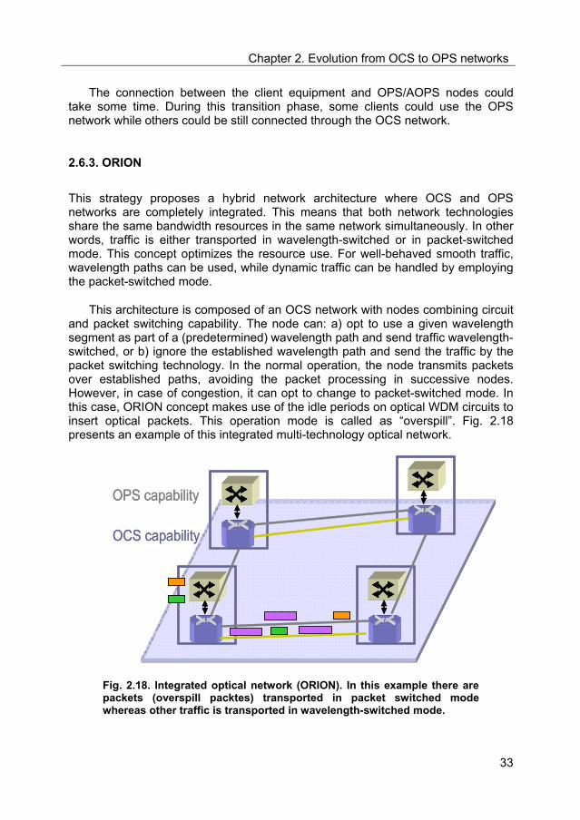
Chapter 2. Evolution from OCS to OPS networks
33
The connection between the client equipment and OPS/AOPS nodes could take some time. During this transition phase, some clients could use the OPS network while others could be still connected through the OCS network.
2.6.3. ORION
This strategy proposes a hybrid network architecture where OCS and OPS networks are completely integrated. This means that both network technologies share the same bandwidth resources in the same network simultaneously. In other words, traffic is either transported in wavelength-switched or in packet-switched mode. This concept optimizes the resource use. For well-behaved smooth traffic, wavelength paths can be used, while dynamic traffic can be handled by employing the packet-switched mode.
This architecture is composed of an OCS network with nodes combining circuit and packet switching capability. The node can: a) opt to use a given wavelength segment as part of a (predetermined) wavelength path and send traffic wavelength-switched, or b) ignore the established wavelength path and send the traffic by the packet switching technology. In the normal operation, the node transmits packets over established paths, avoiding the packet processing in successive nodes. However, in case of congestion, it can opt to change to packet-switched mode. In this case, ORION concept makes use of the idle periods on optical WDM circuits to insert optical packets. This operation mode is called as “overspill”. Fig. 2.18 presents an example of this integrated multi-technology optical network.
��
�
OPS capability
OCS capability
�
����
��
OPS capability
OCS capability
��
Fig. 2.18. Integrated optical network (ORION). In this example there are packets (overspill packtes) transported in packet switched mode whereas other traffic is transported in wavelength-switched mode.

Chapter 2. Evolution from OCS to OPS networks
34
Alternatively, the choice between the wavelength and packet-switched mode can also be motivated by QoS differentiation, e.g. wavelength-switched for high priority traffic.
Among the discussed migration scenarios, the architecture which combines two network technologies offers new degrees of freedom together optimizing the overall network design. However, it leads to an increasing complexity. Hence, the OCS+OPS hybrid approach seems to be the most feasible solution. But, instead of using a client-server hybrid network, it could be interesting to implement a hybrid network architecture in which all-optical packet-switches and optical cross-connects are installed in parallel networks.
In this migration technique, an intelligent edge node employs the different network technologies individually, or in combination, in order to optimally serve customer service requirements. In particular, wavelength-switched transport services are combined with dynamic packet-switched services. Edge nodes select a network technology based on explicit user request, based on traffic characteristics like bandwidth, expected flow duration, or based on QoS requirements. Virtual optical networks (VON) and polymorphic multi-service optical networks (PMON) describe possible realizations of this class of hybrid networks [Breu05, Qiao00b, Mig04]. Fig. 2.19 illustrates the class of parallel hybrid optical network architectures, with the service edge node selecting the transport service from two optical networks. Here, IP traffic can be either transported in optical bursts/packets or in a continuous byte stream inside an optical path.
Resources for transmission and switching can be either dedicated to or shared among the different network technologies. In both cases, the assignment of network resources to the respective technology can be static or dynamic. The realization presented in Fig. 2.19 has dedicated resources for both transmission and switching.
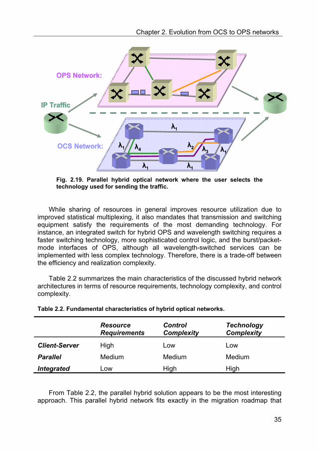
Chapter 2. Evolution from OCS to OPS networks
35
λ1
λ1
λ1
λ1
λ1λ4 λ3
λ2
OPS Network:
OCS Network:
IP Traffic
λ1
λ1
λ1
λ1
λ1λ4 λ3
λ2
OPS Network:
OCS Network:
IP Traffic
Fig. 2.19. Parallel hybrid optical network where the user selects the technology used for sending the traffic.
While sharing of resources in general improves resource utilization due to improved statistical multiplexing, it also mandates that transmission and switching equipment satisfy the requirements of the most demanding technology. For instance, an integrated switch for hybrid OPS and wavelength switching requires a faster switching technology, more sophisticated control logic, and the burst/packet-mode interfaces of OPS, although all wavelength-switched services can be implemented with less complex technology. Therefore, there is a trade-off between the efficiency and realization complexity.
Table 2.2 summarizes the main characteristics of the discussed hybrid network architectures in terms of resource requirements, technology complexity, and control complexity.
Table 2.2. Fundamental characteristics of hybrid optical networks.
Resource Requirements
Control Complexity
Technology Complexity
Client-Server High Low Low
Parallel Medium Medium Medium
Integrated Low High High
From Table 2.2, the parallel hybrid solution appears to be the most interesting approach. This parallel hybrid network fits exactly in the migration roadmap that

Chapter 2. Evolution from OCS to OPS networks
36
was derived from the workshop at NOC. Therefore, it is the migration scenario proposed in LASAGNE.
Further optimization of the traffic transport should be done in the higher (electronic) layers of the network. Installation of the multiple layer traffic engineering principle and grooming would allow these layers to produce less bursty traffic and keep the fluctuations to a minimum. Fewer fluctuations make it easier to assign wavelengths and bandwidth to a traffic stream. Also, it will reduce the size of the OPS network and thus improve its scalability and operation.
In the class of parallel hybrid network architectures only edge nodes need to be aware of the different types of network technologies, while intermediate core nodes only switch the respective granularities but do not exploit information about their content. Awaiting for a full all-optical packet switched network, the applications for this hybrid form of OPS and wavelength-switched networks would be high bandwidth services in which the customers could decide to set-up optical paths or send wavelength routed bursts.
2.7. LASAGNE node modification: Performance monitoring and recovery issues
From a technological viewpoint, AOLS is a very promising approach because it enables the routing of packets independently of bitrate and packet length. Moreover, it helps reducing the mismatch between the forwarding speed of the router and the transmission speed of the fiber. However, to bring AOLS to market, network operators must be convinced of its advantages and the opportunities it creates to better serve their clients. Future telecommunication networks will be characterized by bandwidth-intense services which will lead to a significant growth in traffic volume. In particular, the most demanding user services will be focused on: a) multimedia applications encompassing all services related to voice, video, and data transfer; b) storage applications which transfer massive amounts of data as requested by storage area network (SAN) and disaster recovery actions; and c) grid applications requiring high availability and bandwidth requirements.
Before facing with the definition of the minimum network requirements for the future OPS networks, the following issues should be taken into account:
What type of traffic will be transported through the OPS network? OPS networks will be a multi-client networks with dynamic traffic patterns.
What will be the maximum delay/jitter? The most stringent requirements are counted in applications that involve real-time transfer (maximum delay: 3-10 ms; maximum jitter: 1 ms). The overall delay experienced by data along the network is given by the sum of

Chapter 2. Evolution from OCS to OPS networks
37
individual delays induced by: a) packetization delay which is the time spent at the edge of the network to build an OPS packet; b) latency of OPS core nodes that, in case of contention-free routing it is only a propagation delay; and c) depacketization delay, time required to extract the client data. Concerning latency requirements, AOLS is compatible with real time and hardly real time applications.
What will be the maximum allowed degradation to fulfil with the QoS requirements? Usually, it must be accomplished the following parameters: BER: 10-12; Packet loss: 0.01. Additionally, monitoring mechanisms must be implemented for signal quality monitoring and, thereby, ensuring the minimum quality requirements.
How could it be supported heterogeneous service requirements in terms of QoS and availability? The availability of a service is defined as the percentage of time the service is available. The availability is crucial in the backbone network because a failure can affect great amount of data traffic. The availability requirements require nodes with high reliability and the deployment of protection/restoration mechanisms. Depending on the user services, the requirements in terms of reaction time and availability can vary. The standard in SDH networks is: reaction time equal to 50 ms and availability between 0.9999 (4/9) and 0.99999 (5/9). For future packet switched networks the intermediate nodes must be included protection/restoration functionalities.
As said previously, the future OPS networks will support a great variety of services ranging from voice data sensitive to network delay to bandwidth-intensive services such as video-on-demand. Future transport layer must implement quality of service applications to ensure that user traffic receive appropriate treatment as they travel through the network in terms of bandwidth, jitter, latency and signal quality. Obviously, from the economical viewpoint, transporting all the traffic with the highest QoS requirements is not feasible. Thereby, future networks must perform crucial functions such as service-differentiation applications, and signal quality characterization for quality of service (QoS) assurance and service level agreement (SLA) fulfilment. In such dynamic scenario, performance management including monitoring, fault detection, and alarming has to be supported on all optical networks.
The current QoS applications are based on bit error rate (BER) measurements. These techniques analyze the statistical information of the received signal to determine the bit error rate. These traditional BER-based monitoring techniques are not appropriate for the future ultra high-speed optical networks due to the O/E conversions that limit the bitrate and their response time. In the LASAGNE network the data remains in the optical domain without going through any O/E conversion. This transparent operation is very promising as it offers high data-rate, provides

Chapter 2. Evolution from OCS to OPS networks
38
flexible switching, and supports multiple type of client. However, fault management and performance monitoring are more complex. To perform these functionalities in the next-generation optical networks, new monitoring techniques operating in the optical domain should be defined. Furthermore, given the dynamic nature of data traffic it would be interesting to propose new techniques exploiting the granularity characteristic of OPS networks. To this end, transporting monitoring information inside the packet would be an effective solution to offer QoS on a packet basis. In following chapters, some optical monitoring techniques proposed in this Thesis for monitoring on a packet level will be presented.
Apart from the QoS provisioning, the signal quality information could work together with the restoration mechanisms to ensure the fulfilment of the quality requirement. In contrast to other packet-switching networks, in all-optical networks recovery schemes should take into account that not only the bandwidth provided on a link defines if an optical path can be routed over that link, but also if the target node of the link is capable of receiving the optical path and routing it further correctly. Then, the network recovery techniques should search for free spare link capacity as well as spare node capacity. In LASAGNE project, an analysis of which recovery mechanisms fit better in this scenario has been carried out.
The network recovery schemes are classified in protection or restoration mechanisms. The former schemes are based on the reservation of network resources and backup path establishment before occurring a failure. Recovery by way of restoration just does the opposite. Restoration uses signalling after the failure to dynamically assign resources along the backup path. Hence, protection offers fast recovery time (milliseconds) whereas restoration presents higher flexibility and efficiency. Recovery mechanisms are also broadly classified as path recovery or link recovery, depending on where the protection switching is done. In path recovery, the end nodes control the recovery so that the whole path is protected. In local recovery, faults are intercepted locally.
In OPS networks the choice of the optimal solution strongly depends on the effect they have on the dimensioning and scalability of OPS nodes. As said before, the protection schemes use pre-defined optical paths. Thereby, the infrastructure must be configured as if all the backup paths were to pass through the backup link at the same time. Due to this, all-optical label swapper of the LASAGNE node require a lot of resources comparing to restoration solutions since in the latter schemes the backup capacity and infrastructure is shared among several paths, as shown in Fig. 2.20.

Chapter 2. Evolution from OCS to OPS networks
39
Bandwidth = MAX( , )
A
B C
D
E
F
G
H
backup LSPs
Protection:
Restoration::
A
B C
D
E
F
G
H
Working LSPs
# Correlators = MAX( , )
Bandwidth= MAX( , )# Correlators = SUM( , )
:
# Correlators
0
100
200
300
400
500
600
700
NO reuse Label +wavelength
Label + Port
End-to-end protection
End-to-end restoration
Link protection
Link restoration
a) b) c)
Fig. 2.20. LASAGNE node dimensioning for the different recovery schemes and for different signalling methods (a) using only the label; (b) using the label and the wavelength; (c) using the label and the input port.
In terms of LASAGNE node dimensioning, Fig. 2.20 depicts that the protection scheme is worse than the restoration scheme and link recovery needs more capacity than path recovery [Cae06]. As the flexibility of an all-optical network is defined by the components available in the node, restoration - with the re-use of components - is not as flexible as it is in the case of packet-switching networks with electronic header processing. Therefore, the most suitable recovery scheme for all-optical label swapping is thus path protection.
In the case of the migration scenarios defined in LASAGNE, and in particular, in the hybrid network architecture with an OPS and OCS layers in parallel, the integration of different technologies creates new challenges with respect to network survivability. In different network layers, recovery mechanisms can be exploited together, but interworking is indispensable in order to optimize the performance of fault management functions. The management plane receives signal quality information and the interworking between layers requires some coordination actions in order to ensure an efficient recovery process. A possible multilayer recovery solution would be as follows: once the failure is detected, the lower network layers are responsible of starting the recovery schemes while the higher layers recovery is based on the definition of some timers which must end before activating the recovery actions. Therefore, the higher layers will not take recovery actions if the lower layers solved the network failures. Otherwise, having finished the timers, the higher layers are in charge of the failure restoration.

Chapter 2. Evolution from OCS to OPS networks
40
The evolution of optical networks seems to tend towards a fully reconfigurable network based on packet switching, where the control plane and management plane must work together to provide network intelligence and to allow dynamic reconfiguration. Thanks to the communication between both planes, there is also an interaction between the recovery mechanisms and monitoring tasks, as commented before (see Fig. 2.21).
ManagementPlane
Control Plane
Mo
nit
ori
ng
Buf
ferin
g
ManagementPlane
Control Plane
Mo
nit
ori
ng
Buf
ferin
g
Fig. 2.21. Interaction between the monitoring subsystem and the control and management planes.
In such a scenario the intermediate network nodes should add new functionalities intimately correlated with the signal quality monitoring. To this end, each intermediate node should include a monitoring subsystem capable of signal quality estimation. The performance information coming from this module is disseminated by the control plane and shared between network nodes to assess the status of all connections. Therefore, the control plane is integrated with performance monitoring functions, requiring the modification of the LASAGNE node as illustrated in Fig. 2.22.

Chapter 2. Evolution from OCS to OPS networks
41
De-mux
AOLS
AOLS
AOLS
AOLS
AWG
De-mux
AOLS
AOLS
AOLS
AOLS
AWG
ContentionResolution
&Multiplex
ContentionResolution
&Multiplex
Monitoring Subsystem
Cont
rol P
lane
Switching
De-mux
AOLS
AOLS
AOLS
AOLS
AWG
De-mux
AOLS
AOLS
AOLS
AOLS
AWG
ContentionResolution
&Multiplex
ContentionResolution
&Multiplex
Monitoring Subsystem
Cont
rol P
lane
Switching
Fig. 2.22. Modification of the LASAGNE node including the monitoring subsystem.
With respect to the initial architecture of the LASAGNE node, the control plane interacts with the dynamically reconfigurable switch fabrics. These switches are responsible for matching an incoming packet to a new label and thus perform inter-node forwarding based on the AOLS concept. In the same way, if a monitoring subsystem is introduced into the node, the signal quality information must be sent to the control plane which interacts with the switching matrices and the wavelength converters to route the packets accordingly to their quality requirements. At this point, an interface between the control plane and the node itself should be defined so that the monitoring information, and in turn, routing decisions made by the control plane have direct impact on the recovery functionalities.
2.7.1. Routing protocol based on quality requirements
As said previously, the monitoring subsystem gives information about the signal quality in real time, allowing to take immediate actions faced with dynamic network changes. Apart from this feature, the monitoring block can also interact with the

Chapter 2. Evolution from OCS to OPS networks
42
routing mechanisms to contribute to the supervision of SLA fulfilment and to efficiently perform routing based on signal quality requirements.
When discussing routing in all-optical networks, it is usually assumed that all routes have adequate signal quality. However, there are strong reasons to consider all-optical networks in which not all routes have the required signal quality. First, as bitrates increase, it is necessary to increase power. This makes impairments caused by nonlinearities more troublesome. Second, the optical technology is advancing very rapidly, making larger networks possible. These considerations will lead to the deployment of a network that is too large to ensure that all routes have adequate signal quality. Therefore, there is a strong necessity of a definition of a protocol that takes into account the impairments effects of an optical layer.
The main goal of the routing protocol is to keep the level of QoS promised to customers. In this protocol the path selection is based on optical signal quality and on information related to the available bandwidth, leading to more optimized solutions. This approach facilitates the recovery of paths with poor quality, and enables the implementation of traffic engineering algorithms.
The protocol combines intelligent routing with the immediate information about signal quality provided by the monitoring module located inside the intermediate nodes. The performance information coming from this module is then disseminated by the control plane and shared among network nodes to assess the status of all connections. Hence, the quality estimation is added as an additional factor in the routing decision. Moreover, information about the available bandwidth is added as a cost factor. By using the quality and the cost factors, the control plane establishes the optimum path.
Fig. 2.23 shows an example of the routing protocol based on quality information [And04]. In this example, a new optical path is established from the node A to the node B. Each intermediate node assesses the cost factor and estimates the signal quality. According to these two factors, the destination node selects the optical path with the required quality and the lowest cost.

Chapter 2. Evolution from OCS to OPS networks
43
5040
80
100
750.42003
0.71752
0.72201
QualityCostPathNode B
50
70
Node A
5040
80
100
750.42003
0.71752
0.72201
QualityCostPathNode B
50
70
Node A
Fig. 2.23. Routing protocol based on signal quality requirements. The nodes exchange information about the quality and cost of each connection (The figure shows the cost of each link).
2.8. Summary and conclusions
The increasing demand in the Internet network for real-time multimedia data traffic with high quality is pushing the limits of existing network structure. Furthermore, the introduction of new dynamic bandwidth-intensive applications requires more dynamic bandwidth offer and reservation, and more flexibility on the resource assignment. Indeed, when video and TV services are mature, the demand for bandwidth from these applications will be characterized by very short duration transmissions requiring very high capacity. In such a highly dynamic scenario, the OPS networks will provide the flexibility and efficiency required.
At the beginning of this Chapter, the motivations of the evolution towards such networks have been underlined, showing the trend towards a simplified network architecture with IP packets switched and routed over DWDM layer based on packet switching technology. Later, the principle of operation of the OPS networks has been described. In these networks, the optical packets are transparently switched in the intermediate nodes while the optical label is electronically processed for routing decisions. The functional blocks comprising the optical packet switching node have been presented as well.
However, as the bitrates increase, electronic processing would not be able to handle the routing of a massive number of packets per second, which could easily lead to router congestion. All-optical processing appears to be a promising solution to avoid this bottleneck imposed by the O/E conversions. In this context, the LASAGNE project proposes a novel node and network architecture based on the AOLS concept. The main goal of this project is not only to optically switch the packet, but also perform the header processing in the optical domain.

Chapter 2. Evolution from OCS to OPS networks
44
In LASAGNE two options for the design of the OPS network made up of all-optical packet nodes have been proposed. The former approach consists of a pure packet-switched network which means that the packet switching nodes are connected directly using WDM links. The latter solution is based on a mixed packet-circuit approach where an optical packet layer and underlying optical circuit layer exist. As seen in this Chapter, the last option facilitates the migration from the current network architectures towards the final OPS solution.
In the discussion of the OPS solution, two types of nodes can be distinguished: a) core nodes responsible of packet and header processing and routing tasks; and b) edge routers responsible of inserting the client protocol data units in optical packets. To enable the translation of the user requirements into information used by OPS network, a mapping procedure is defined. In this Chapter, the design of both nodes has been described.
Despite the advances in optical technologies, the deployment of a truly all-optical network is still considered to be a distant future. The main focus lies with the design of a migration path from current networking technologies towards all-optical packet switching networks. In LASAGNE, a workshop focused on the migration technologies and strategies was organized. From the conclusions drawn in this workshop, several migration scenarios based on hybrid OCS/OBS/OPS solutions have been proposed. Among all the proposed scenarios, architecture integrating two network technologies opens new degrees of freedom to bring packets and circuits closer together optimizing the overall network design. However, this implies an extra complexity so that the hybrid solution with OCS and OPS layers in parallel seems to be more feasible. In fact, the network architecture should consist of a smaller OPS network and a bigger wavelength-switched part. This would allow for scalable network design and optimize traffic transport. Further optimization of traffic transport should be done in higher layers of the network.
Finally, given the next-generation service requirements, it is necessary to ensure that networks are performing at the desired level and thereby realizing a reliable, high-performance and service-differentiation enabled all-optical network. At this point, performance monitoring and the implementation of fast recovery mechanisms are especially important. In LASAGNE, the node has been modified to include a monitoring subsystem responsible of signal quality estimation. This monitoring information is sent to the control plane and disseminated among networks nodes to infer the state of the network. Furthermore, the control plane and the management plane work together to dynamically reconfigure the connections as a response to network changes. This interaction leads to the integration between the monitoring module and recovery mechanisms, which means that when a failure or reduction in the signal quality is detected, the recovery mechanisms are activated.
On the other hand, this monitoring information could also be used for collaborating with routing functions by establishing new optical paths according to

Chapter 2. Evolution from OCS to OPS networks
45
the estimated quality. The performance monitoring on a packet-by-packet basis brings about new challenge so that new monitoring techniques operating in the optical domain must be defined. This topic is the main focus of this Thesis and it will be addressed in successive Chapters, where new optical solutions for OPS networks will be investigated.

Chapter 2. Evolution from OCS to OPS networks
46
2.9. References
[Ais03] S. Aisawa, A. Watanabe, T. Goh, Y. Takigawa, M. Koga, and H. Takahashi, “Advances in optical path cross-connect system using planar-lightwave circuit-switching technologies,” IEEE Commun. Mag., vol. 41, pp. 54-57, 2003.
[And04] B.L. Anderson, A. Durresi, D. Rabb, and F. Abou-Galala, “Real-time all-optical quality of service monitoring by use of correlation and a network protocol to exploit it,” Applied Optics, vol. 43, no. 5, pp. 1121-1130, 2004.
[Awd01] D. Awduche, and V. Rekhter, “Multiprotocol lambda switching: combining MPLS traffic engineering control with optical cross-connects,” IEEE Commun. Mag., vol. 39, no. 3, pp 111-116., 2001.
[Ban01] A. Banarjee, J. Drake, J.P. Lang, B. Turner, K. Kompella, and Y. Rekhter, “Generalized multiprotocol label switching: an overview of routing and management enhancements,” IEEE Commun. Mag., vol. 39, no. 7, pp. 144-151, 2001.
[Blu00] D.J. Blumenthal, B.E. Olsson, G. Rossi, T.E. Dimmick, L. Rau, M. Masanovic, O. Lavrova, R. Doshi, O. Jerphagnon, J.E. Bowers, V. Kaman, L.A. Coldren, and J. Barton, “All-optical label swapping networks and technologies,” IEEE/OSA J. Lightwave Technol., vol. 18, no. 12, pp. 2058-2075, 2000.
[Blu03] D.J. Blumenthal, J.E. Bowers, L. Rau, H.F. Chou, S. Rangarajan, W. Wang, and H.N. Poulsen, “Optical signal processing for optical packet switching networks,” IEEE Commun. Mag., vol. 41, no.2, pp. 23-29, 2003.
[Breu05] E. Van Breusegem, “Study and design of hybrid optical network architectures,” PhD Thesis (2005), ISBN: 90-8578-061-6.
[Breu06] E. Van Breusegem, “Overspill routing in optical networks: a true hybrid optical network design,” IEEE J. Selected Areas in Communications, vol. 24, no. 4, pp. 13-25, 2006.
[Cae06] R. Van Caenegem, D. Roccato, and R. Vilar “Evolution towards an all-optical switched packet networks: the LASAGNE viewpoint,” in Proc.of 11th European Conference on Networks and Optical Communications (NOC’06), Berlin (Germany), 2006.
[Cal99] R. Callon, “A framework for Multi-Protocol Label Switching,” IETF-MPLS, 1999.
[Cap06] J. Capmany, B. Ortega, “Redes Ópticas,” Editorial UPV, 2006.
[Car98] A. Carena et al., “OPERA: An Optical Packet Experimental Routing Architecture with Label Swapping Capability,” IEEE/OSA J. Lightwave Technol., vol. 16, no. 12, pp. 2135, 1998.

Chapter 2. Evolution from OCS to OPS networks
47
[Chia01] D. Chiaroni, “Status and applications of optical packet switching,” in Proc. of 27th European Conference on Optical Communication (ECOC’01), Amsterdam (The Netherlands), 2001.
[Dit03] L. Dittmann, C. Develder, D. Chiaroni, F. Neri, F. Callegati, W. Koerber, A. Stavdas, M. Renaud, A. Rafel, J. Sole-Pareta, W. Cerroni, N. Leligou, L. Dembeck, B. Mortensen, M. Pickavet, N. Le Sauze, M. Mahony, B. Berde, and G. Eilenberger, “The European IST project DAVID: a viable approach towards optical packet switching,” IEEE J. Selected Areas in Communications”, vol. 32, no. 7, pp. 1026-1040, 2003.
[Dor03] H.J.S. Dorren, M.T. Hill, Y. Liu, N. Calabretta, A. Srivatsa, F.M. Huijskens, H. de Waardt, and G.D. Khoe, “Optical packet switching and buffering by using all-optical signal processing methods,” IEEE/OSA J. Lightwave Technol., vol. 21, no. 1, pp. 2-12, 2003.
[Düs02] M. Düser, and P. Bayvel, “Analysis of a dynamically wavelength-routed optical burst switched network architecture,” IEEE/OSA J. Lightwave Technol., vol. 20, no. 4, pp. 574-585, 2002.
[Flo95] J.E. Flood, “Telecommunication switching, traffic and networks,” Ed. Prentice Hall, 1995.
[Gam98] P. Gambini, M. Renaud, C. Guillemot, F. Callegati, I. Andonovic, B. Bostica, D. Chiaroni, G. Corazza, S.L. Danielsen, P. Gravey, P.B. Hansen, M. Henry, C. Janz, A. Kloch, R. Krähenbühl, C. Raffaelli, M. Schiling, A. Talneau, and L. Zucchelli, “Transparent optical packet switching: network architecture and demonstrators in the KEOPS project,” IEEE J. Selected Areas in Communications, vol. 16, pp. 1245-1259, 1998.
[Gha00] N. Ghani, S. Dixit, and T.S. Wang, “On IP over WDM integration,” IEEE Commun. Mag., vol. 38, no. 3, pp. 72-83, 2000.
[Gui98] C. Guillemot, M. Renaud, P. Gambini, C. Janz, I. Andonovic, R. Bauknecht, B. Bostica, M. Burzio, F. Callegati, M. Casoni, D. Chiaroni, F. Clérot, S.L. Danielsen, F. Dorgeuille, A. Dupas, A. Franzen, P.B. Hansen, D.K. Hunter, A. Kloch, R. Krähenbühl, B. Lavigne, A. Le Corre, C. Raffaelli, M. Schilling, J.C. Simon, and L. Zucchelli, ”Transparent optical packet switching: the European ACTS KEOPS project approach,” IEEE/OSA J. Lightwave Technol., vol. 16, no. 12, pp. 2117-2134, 1998.
[Hill01] A. Hill, and F. Neri,”Optical switching networks: from circuits to packets,” IEEE Commun. Mag., vol. 39, no. 3, pp. 107-108, 2001.
[Hos02] M. Hossain, “An overview of ITU-T G. 709,” Agilent Technologies, 2002.
[Hun99] D. Hunter, et al.,”WASPNET: A Wavelength Switched Packet Network,” IEEE Commun. Mag., vol. 37, no. 3, pp. 120-129, 1999.

Chapter 2. Evolution from OCS to OPS networks
48
[Hun00] D. Hunter, and I. Andanovic, “Approaches to Optical Internet packet switching,” IEEE Commun. Mag., vol. 38, no. 7, pp. 116-122, Sept. 2000.
[Jou01] A. Jourdan, D. Chiaroni, E. Dotaro, G.J. Elienberger, F. Masetti, and M. Renaud, “The perspective of optical packet switching in IP-dominant backbone and metropolitan networks,” IEEE Commun. Mag., vol. 39, no. 3, pp. 136-141, 2001.
[Keh06] E. Kehayas, D. Tsiokos, P. Bakopoulos, D. Apostolopoulos, D. Petrantonakis, L. Stampoulidis, A. Poustie, R. McDougall, G. Maxwell, Y. Liu, S. Zhang, H.J.S. Dorren, J. Seoane, P. Van Holm-Nielsen, P. Jeppensen, and H. Avramopoulos, ”40-Gbit/s all-optical self-routing node and network architecture employing asynchronous bit and packet level optical signal processing,” IEEE/OSA J. Lightwave Technol., vol. 24, no. 8, pp. 2967-2977, 2006.
[Kit03] K. Kitayama, and M. Murata, ”Versatile optical code-based MPLS for circuit, burst and packet switching,” IEEE/OSA J. Lightwave Technol., vol. 21, no. 11, pp. 2753-2764, 2003.
[Koga04] M. Koga, T. Morioka, and Y. Miyamoto, “Next generation optical communication technologies for realizing bandwidth networking capability,” Optical Review, vol. 11, no. 2, pp. 87-97, 2004.
[Koo01] T. Koonen, G. Morhier, J. Jennen, H. De Waart, P. Demeester, “Optical packet routing in IP-over-WDM networks deploying two-level optical labelling,” in Proc. of 27th European Conference on Optical Communication (ECOC’01), vol. 4, pp. 608-609, Amsterdam (The Netherlands), 2001.
[Mah01] M.J. O’Mahony, D. Simeonidou, D. Hunter, and A. Tzanakaki, “The application of optical packet switching in future communication networks,” IEEE Commun. Mag., vol. 39, no. 3, pp. 128-135, 2001.
[Mar04] J.M. Martinez, F. Ramos, and J. Marti, “All-optical header processor based on cascaded SOA-MZIs,” Electron. Lett., vol. 40, no. 14, pp. 894-895, 2004.
[Mar06] J.M. Martinez, J. Herrera, F. Ramos, and J. Marti, “All-optical address recognition scheme for label-swapping networks,” IEEE Photon. Technol. Lett., vol. 18, no. 1, pp. 151-153, 2006.
[Mig04] I. de Miguel, J.C. Gonzez, T. Koonen, R. Dur, P. Ferndez, and I.T. Monroy, “Polymorphic architectures for optical networks and their seamless evolution towards next generation networks,” Photon. Net. Commun., vol. 8, no. 2, 2004.
[Mod99] E. Modiano, “WDM-based packet networks,” IEEE Commun. Mag., vol. 37, no. 3, pp. 130-135, 1999.
[Qiao99] C. Qiao, and M. Yoo, “Optical Burst Switching (OBS) - A new paradigm for an optical Internet,” J. High Speed Networks, vol. 8, pp. 69-84, 1999.
Chapter 2. Evolution from OCS to OPS networks
49
[Qiao00a] C. Qiao, and M. Yoo, “Choices, features and issues in optical burst switching,” Optical Networks Magazine, vol. 1, no. 2, pp. 37-44, 2000.
[Qiao00b] C. Qiao, “Polymorphic control for cost-effective design of optical networks,” European Transactions on Telecommunications, vol. 11, no. 1, pp. 17-26, 2000.
[Ram05] F. Ramos, E. Keheyas, J.M. Martinez, R. Clavero, J. Marti, L. Stampoulidis, N. Chi, P. Jeppesen, N. Yan, I.T. Monroy, A.M.J. Koonen, M.T. Hill, Y. Liu, H.J.S. Dorrer, R. Van Caenegem, D. Colle, M. Pickavet, and B. Riposati, “IST-LASAGNE: Towards all-optical label swapping employing optical logic gates an optical flip-flops,” IEEE/OSA J. Lightwave Technol., vol. 23, no. 10, pp. 2993-3001, 2005.
[Ren97] M. Renaud, F. Masetti, C. Guillemot, and B. Bostica, “Network and system concepts for optical packet switching,” IEEE Commun. Mag., vol. 35, no. 4, pp. 96-102, 1997.
[Ros01] E. Rosen, “Multiprotocol label switching architecture,” IETF RFC 3031, 2001.
[Sato02] K.I. Sato, N. Yamanaka, Y. Takigawa, M. Koga, S. Okamodo, K. Shomodo, F. Oki, and W. Imajuku, “GMPLS-based photonic multilayer router (Hikari router) arcuitecture: An overview of traffic engineering and signalling technology,” IEEE Commun. Mag., vol. 40, no. 3, pp. 96-101, 2002.
[Tuck99] R.S. Tucker, and W.D. Zhong, “Photonic packet switching: An overview,” IECE Trans. Commun., vol. E82-B, no. 2, 1999.
[Vla03] K.G. Vlachos, I.T. Monroy, A.M.J. Koonen, C. Peucheret, and P. Jeppesen, “STOLAS: Switching technologies for optically labeled signals,” IEEE Commun. Mag., vol. 41, no. 11, pp. 43-49, 2003.
[Yao00] S. Yao, B. Mukherjee, and S. Dixit, “Advances in photonic packet switching: an overview,” IEEE Commun. Mag., vol. 38, no. 2, pp. 84-94, 2000.
[Yao01] S. Yao, S.J.B. Yoo, and B. Mukherjee, “All-optical packet switching for metropolitan area networks: opportunities and challenges,” IEEE Commun. Mag., vol. 39, no. 3, pp. 142-148, 2001.
[Yoo01a] M. Yoo, C. Qiao, and S. Dixit, “Optical burst switching for service differentiation in the next-generation optical Internet,” IEEE Commun. Mag., vol. 39, no. 2, pp. 98-104, 2001.
[Yoo01b] S.J.B. Yoo, “Optical label switching, MPLS, MPLambdaS and GMPLS,” in Proc. of Asia-Pacific Optical and wireless Communications (APOC’01), vol. 4585, pp. 1-11, 2001.
[Yoo01c] S.J.B. Yoo, H. Lee, S.K.H. Fong, V. Tsui, and Y. Zhang, “Demonstration of optical packet switching using optical label switching technologies,” in Proc. of
Chapter 2. Evolution from OCS to OPS networks
50
SPIE, vol. 4582, pp. 121-132, 2001.
[Yoo05] S.J.B. Yoo. “Optical-label based packet, burst and circuit switching networks,” in Proc. of SPIE, vol. 5626, pp. 68-77, 2005.
[Yoo06] S.J.B. Yoo, “Optical packet and burst switching technologies for future photonic Internet,” IEEE/OSA J. Lightwave Technol., vol. 24, no. 12, pp. 4468-4491, 2006.
51
Chapter 3
Optical performance monitoring in optical networks. State of the art
3.1. Introduction
During the last decades, optical transport systems have become the suitable solution to enable the rapid growth of data traffic in the network backbone. Apart from enhancing the network capacity, optical networks allow high bitrates but at the expense of increasing the complexity of the network management.
Due to the increased transparency and the data bitrate, the quality of signals becomes more vulnerable to the optical layer impairments such as ASE noise, fiber nonlinearities, residual chromatic dispersion (CD), polarization mode dispersion (PMD), and so on. Thus, for the proper operation and management of the future dynamic optical networks, it is indispensable to have the capability to monitor the parameters affecting networks performances directly in the optical layer. Furthermore, the new optical layer functionalities including dynamic reconfiguration and optical path restoration add new challenges in the implementation of monitoring functions in the optical domain. All of these issues bring focus to optical performance monitoring (OPM) as an enabling technology for next generation optical networks. In fact, OPM is a potential mechanism capable of improving the control of transmission and physical layer fault management [Ben00, Kil04a] which results in enhancing the network reliability.

Chapter 3. Optical performance monitoring in optical networks. State of the art
52
The potential applications of OPM include the network elements control (e.g. to provide feedback signals for tunable compensators), optical path setup, link selection based on physical constraints, signal quality assessment (for QoS assurance), fault detection and localization, and activation of the restoration mechanisms. To date, numerous optical performance monitoring techniques have been proposed and demonstrated for these applications. However, next-generation optical networks require new techniques capable of real-time monitoring to immediately react to signal failure or signal degradation, which existing techniques cannot offer.
This Chapter presents a deep revision of the state of the art of the existing techniques in the literature. Section 2 gives the definition of optical performance monitoring and the main optical impairments imposed by the fiber. In Section 3 the main architectures and monitoring technologies are described, explaining their principles of operation as well as their main advantages and disadvantages. This revision is a first step towards the implementation of OPM applications in all-optical packet-switched networks. In Section 4 the main motivations of using the monitoring on a packet level are addressed and finally, the basis of the monitoring techniques presented in this Thesis is discussed.
3.2. Optical performance monitoring
Despite the fact that optical networks have enabled the rapid growth of data traffic, the optical impairments imposed by the fiber degrade the network performances and limit the deployment of high speed optical transmissions. Moreover, the trend of optical network towards a fully reconfigurable network demands the integration of OPM functions with the control and the management plane to perform a reliable, high-performance and service-differentiation all-optical network.
Thanks to this interaction, the blocks responsible of the signal quality monitoring can play a major role to perform other functions including: a) OPM can provide information for fault management which consists of identification, localization, diagnosis, and tracking of faults in a network [Kil05]; b) OPM can be used as a feedback to keep the network operating in an optimal manner [Kil04a]; c) OPM can perform the signal quality monitoring for quality of service assurance; d) OPM can act as an alarm to predict network failures and allows traffic to be rerouted before failure occurs [Ric02]. Together with these applications related to quality monitoring and failure tracking, OPM can also assist the control plane to detect and dynamically set up optical paths taking into account the physical impairments, as commented in the previous Chapter [Tei09]. Therefore, OPM is essential for managing the future optical networks since it includes a wide range of functionalities focused on improving network performances.

Chapter 3. Optical performance monitoring in optical networks. State of the art
53
The broad spectrum of OPM includes a plethora of parameters to be monitored which can be classified into three categories as shown in Fig. 3.1.
OPM
SignalLoss
SignalAlignment
SignalQuality
In-lineComponent
Failures
FiberCuts
Tx/RxFailures
EDFAFailures
Othercomponent
Failures
Wavelength
PulseCarver
Filter
DigitalParameters
AnalogParameters
BER OSNR
Jitter
PMDOpticalPower
CD Eyediagram
NonlinearDistortion
ExtinctionRatio Q- factor
OPM
SignalLoss
SignalAlignment
SignalQuality
In-lineComponent
Failures
FiberCuts
Tx/RxFailures
EDFAFailures
Othercomponent
Failures
Wavelength
PulseCarver
Filter
DigitalParameters
AnalogParameters
BER OSNR
Jitter
PMDOpticalPower
CD Eyediagram
NonlinearDistortion
ExtinctionRatio Q- factor
OSNR
Jitter
PMDOpticalPower
CD Eyediagram
NonlinearDistortion
ExtinctionRatio Q- factor
Fig. 3.1. The broad spectrum of OPM.
The first category refers to the monitoring of in-line components failures and fiber cuts that cause the signal loss. Second, signal alignment monitoring concerns with the alignment of signal wavelength, filter position, and pulse carver to ensure proper operation. Finally, signal quality monitoring pertains to the monitoring of a multitude of effects degrading the signal that must be minimized or controlled.
The fiber cut monitoring is necessary to avoid the huge data loss when a fiber failure occurs. To this end, passive optical surveillance schemes based on fiber Bragg gratings (FBG) have been proposed in the literature. Spectral analysis with Fast Fourier Transform (FFT) has also been presented to perform this task [Cha97, Wan04]. On the other hand, in-line active component monitoring is important to keep the network operating in an optimal manner. The components faults include individual or multiple component malfunctions, and improperly installed or configured equipment. In [Kar01] the more common component failure modes have

Chapter 3. Optical performance monitoring in optical networks. State of the art
54
been catalogued. The use of FBG, pilot tones, and spectral analysis has also been proposed to carry out the monitoring [Kon99, Chan02].
Apart from the failures mentioned before, there are other intrinsic effects of the optical transmissions that must be controlled and minimized. In OCS networks the signal quality is monitored by measuring parameters such as channel power [Chen03], aggregate power, channel wavelength, and spectral optical signal-to-noise ratio [Chen05]. Given the increasing transparency and the reconfigurability requirements, the future optical networks require the definition of advanced techniques capable of monitoring in such dynamic scenario. Thus, to implement OPM in an optical system, it is necessary to monitor characteristic optical layer parameters. These parameters can be divided into two categories: linear and nonlinear impairments. This classification is based on the dependency on the signal power [Chu00]. In the case of linear parameters, they are independent of the transmitted signal power, whereas nonlinear impairments are more complex, and very hard to quantify as they depend on a combination of factors such as signal power, number of wavelengths per channel, and the channel bandwidth. Commonly, the effect of the linear parameters is dominant. That is why it is usually assumed that the nonlinear impairments are negligible. Hence, the monitoring techniques are focused on the measurement of the following linear parameters:
Optical Signal-to-Noise Ratio (OSNR): Optical amplifiers have become essential components in optical networks to compensate the transmission losses. In addition to providing optical gain, these amplifiers add undesired noise onto the amplified signal, which is called amplified spontaneous emission (ASE) noise [Des94]. ASE is directly proportional to the signal power and inversely proportional to the amplifier gain and link bandwidth. The spectrum of the background noise is often wide, and thereby some of that noise can cause the signal to get impaired due to the interference between the signal and the noise. This noise affects the receiver ability to properly decode the optical signal and thus introduces errors. The noise is quantified in terms of the OSNR, which is defined as:
noise
signal
P
POSNR , (3.1)
where Psignal is the optical signal power, and Pnoise is the optical noise power. The higher the OSNR is, the better the signal quality. This measure is very frequently defined as a design factor when determining the quality of service (QoS) requirements of an optical link.
Q-factor/BER [Noi02, Kil04b]: A bit error occurs when a transmitted signal gets so corrupted that causes the reception of a ‘0’ when a ‘1’ is

Chapter 3. Optical performance monitoring in optical networks. State of the art
55
transmitted or viceversa. The bit error rate (BER) is a statistical measure of how often these errors occur. This parameter is the most preferred one for fault management as it uses the same metric as determining the QoS at end-terminals. However, the BER measurements to be statistically significant require a lot of time, several seconds or several minutes, making them inappropriate for future high-speed optical networks. At this point, the eye diagram provides a faster solution. An eye diagram is constructed by superimposing bit sequences. This process can take several milliseconds. The results obtained from the eye diagram are related to the BER of the transmitted signal through the quality factor or Q-factor of the signal, which is defined by adjusting the receiver decision threshold to an optimal value. The mathematical expressions are given by:
22
1 QerfcBER , being
01
01
Q , (3.2)
where x and x are the mean value and the standard deviation and the subscript x denotes the bit value of 0 or 1. Given the strong correlation between the BER and the Q-factor, this parameter is often used for signal quality monitoring.
Chromatic dispersion (CD): Dispersion is a temporal effect that results in pulse broadening and consequently in errors at the receiver. This effect is one of the most limiting factors at high speeds. Chromatic dispersion is the term given by which different spectral components of a pulse travel at different velocities [Ram02]. The chromatic dispersion is caused by the dependence of the refractive index of the transmission medium on the frequency components present in the transmitted signal. The CD for a uniform medium can be calculated as:
2
2
d
nd
cCD , (3.3)
where λ is the wavelength of the transmitted signal, c is the speed of the light, and n is the refractive index of the uniform medium.
Polarization Mode Dispersion (PMD): PMD is caused by the asymmetry of the fiber core, in which light polarized in one axis travels slightly faster than light polarized in the orthogonal axis [Gor00]. Pulse spreading arises due to the differential light speed and causes inter-

Chapter 3. Optical performance monitoring in optical networks. State of the art
56
symbol interference (ISI) which results in increased bit error rate. Therefore, PMD is, together with chromatic dispersion, one of the key limitations in the deployment of optical systems transmitting at 10 Gbit/s or beyond. The first-order PMD is called differential group delay (DGD) and represents the temporal delay between the principal polarization modes of the fiber. The DGD of the fiber is described by:
LDDGD PMD , (3.4)
where L is the fiber link, and DPMD is the fiber PMD parameter
measured in ps/ km . The unit for DGD is ps [Poo97]. On the other hand, second-order of PMD describes the wavelength dependence of the DGD and has two components: depolarization and polarization dependent chromatic dispersion. This second-order factor causes the principal polarization modes to broaden.
Jitter: Jitter is defined as a variation in the signal characteristics between consecutive pulses such as a variation in the pulse width and/or phase of the pulse [Fis56]. Commonly, the temporal variations such as the change in the pulse interval or shift in the pulse peak are considered. This parameter is hard to monitor and compensate. The BER measurement is sensitive to this impairment and can be used for identifying the jitter source.
Once defined the most important parameters to be monitored for signal quality monitoring, the most important technologies implemented in the current OCS networks are described in the next section. Later, the need for advanced monitoring arose from the deployment of dynamically reconfigurable networks is highlighted and a deep review of the existing techniques is presented.
3.3. Current OPM technologies for transparent circuit switched networks
Monitoring techniques have been used in optical systems for detecting the fiber and component failures and providing feedback signals for adaptive compensators. Recently, these techniques have also been widely used for monitoring the signal quality such as channel power and wavelength of each WDM channel, and for estimating the OSNR. In this section, an overview of the available optical performance monitoring schemes is given. At present, there are predominantly two different OPM techniques available on the market: optical spectrum analyzer devices using Bragg gratings (OCM-SR, Princeton Lightwave) [OCM] or tunable

Chapter 3. Optical performance monitoring in optical networks. State of the art
57
filters as diffraction devices, and polarization-nulling based devices (Argos N401, Teralink Communications) [N401].
3.3.1. Optical Spectrum Analyzer (OSA)
The traditional optical spectrum analyzer (OSA) is based on analyzing the optical spectrum of the detected signal. This monitor uses a narrow band tunable optical filter device to resolve the individual channel power, wavelength and noise. The OSA-based OSNR estimation relies on interpolation of ASE levels adjacent to the channel to obtain the approximate ASE level in the channel, as shown in Fig. 3.2.
Channel 3
Channel 2
Channel 1 Channel 3
Channel 2
Channel 1
Fig. 3.2. Diagram of linear interpolation of ASE.
The main limitation of the out-of-band OSNR technique is that it assumes the power levels on both sides of the channel are equal to the in-channel noise level which becomes invalid for the dynamically reconfigurable WDM networks as the interpolated ASE noise may not be the real in-band ASE noise due to signal overlap form neighbouring channels, in-line filters, etc. Thus, investigating alternative schemes to estimate the in-band OSNR has been highly motivated. Concretely, a technique based on polarization-nulling of optical signal has been proposed.
3.3.2. Polarization nulling
The polarization-nulling method overcomes some of the OSA limitations in OSNR measurements. This technique utilizes the different properties of optical signal and ASE noise for accurate monitoring of the OSNR in optical networks. Concretely, it is assumed that an optical signal is completely polarized whereas noise contributions are completely non-polarized. The optical signal and ASE noise pass

Chapter 3. Optical performance monitoring in optical networks. State of the art
58
through a polarization controller. Then the optical power is measured by an optical power meter. When the polarization controller is set to the orthogonal polarization state as the signal, the power meter indicates a minimum value which corresponds to the half of the ASE noise. Otherwise, when the polarization controller is set to the same polarization state as the signal, the power meter indicates a maximum value (Psignal + 0.5Pnoise). By comparing the maximum and minimum detected values, the OSNR can be estimated [Lee01].
As said before, the polarization-nulling technique utilizes different polarization properties of the optical signal and ASE noise. As a result, the performance of this technique is bound to be affected by various polarization effects that occurred in the transmission link [Xie05, Lee06]. In fact, this technique becomes erroneous if the signal is depolarized due to PMD [Lee01]. Apart from the PMD effect, the optical signal could also be depolarized by nonlinear birefringence [Phi99, Phi05]. This effect would result in the overestimation of the noise power and cause monitoring errors. In addition, the accuracy of this technique could also be deteriorated if the ASE noise becomes polarized due to polarization-dependent loss (PDL) since the noise power in the orthogonal polarization state may no longer be identical to the noise in the state parallel to the signal [Feu05].
Therefore, for practical use, it is necessary to improve the polarization-nulling technique so that it could endure the effects of PMD and nonlinear birefringence. Several techniques have been proposed for this purpose [Lee01b, Chung04, Cheun04, Choi06]. These techniques either calibrate out the small amount of signal power leaked into the noise in the orthogonal polarization state (due to PMD or nonlinear birefringence) by using an additional optical filter or measure the noise power at the side of the signal spectrum to mitigate the effects of PMD or nonlinear birefringence. The results showed that these techniques could monitor the OSNR with accuracy of better than ±1 dB, even when the first-order PMD was as large as 60 ps. However, those additional components increase the complexity and cost of the monitor as well as limiting the speed of the OSNR monitoring.
With the trend of optical networks towards dynamically reconfigurable optical networks, the previous monitoring techniques do not provide the necessary accuracy and the time response for such dynamic scenario. Therefore, new advanced monitoring techniques must be defined.
3.4. Advanced OPM concepts for dynamically reconfigurable networks
The need for advanced monitoring arose from the increase of the network transparency and the development of dynamically reconfigurable networks where optical signals might traverse different paths and different components. Thus, for the proper operation and management of such dynamic WDM networks, it is

Chapter 3. Optical performance monitoring in optical networks. State of the art
59
indispensable to propose advanced optical performance monitoring techniques based on monitoring the physical parameters which affect network performances such as OSNR, chromatic dispersion, Q-factor, and PMD. This section focuses on the analysis of performance monitoring techniques applicable to dynamically reconfigurable networks. In particular, the analysis is structured into the following categories: RF spectrum analysis, sampling techniques, techniques based on interferometric configurations, polarization-based methods, and the use of nonlinear effects for monitoring tasks.
3.4.1. RF spectrum analysis
The RF spectrum provides a measure of signal quality since it measures the spectrum of the signal encoded on the optical carrier. Noise and distortion on the amplitude power spectrum (i.e, RF spectrum) will usually directly translate to impairments on the signal. Within the RF-spectrum-based techniques, two main categories can be distinguished: pilot-tone-based and clock-tone-based techniques.
3.4.1.1. Pilot tones
Many monitoring techniques based upon the RF spectrum are based on the use of spectral tones. These narrowband monitor signals are superimposed on data signal and used as monitoring probes. The most common low-frequency technique involves placing an RF sinusoidal modulation on the optical signal at the transmitter. The strengths of this approach lie in the simplicity of using double sideband subcarrier signal transmission and the fact that these signals travel the complete optical path with the baseband signal so that are subject to the same degradations as the baseband signal. Additionally, since a unique subcarrier frequency can be allocated to each wavelength, the optical path of each WDM signal can be simply monitored by tracking its corresponding tone frequency.
On the other hand, the pilot tone can be extracted at intermediate nodes by means of simple electronic circuit and can be utilized for monitoring various optical parameters such as OSNR, chromatic dispersion and PMD, as commented below.
a) OSNR monitoring. A simple way to monitor the OSNR is to place a high-frequency pilot tone outside of the signal bandwidth. Since there should be no signal component in this frequency region, the OSNR could be estimated simply by measuring the carrier-to-noise ratio (CNR) of the pilot tone at the receiver [Ross00, Ji04]. However, the pilot tone performance is affected by the number of wavelengths operating in the network, the frequencies used, the modulation index, and the measurement is sensitive to both CD and PMD [Ham97]. These limitations cause inaccuracy of the

Chapter 3. Optical performance monitoring in optical networks. State of the art
60
OSNR measurement. Therefore, further study is needed to improve the accuracy of the pilot-tone-based OSNR monitoring technique for its practical use.
b) CD monitoring. As the subcarrier signal traverses a dispersive fiber link, the lower and upper sidebands of the optical signal experience a relative phase delay that increases with the accumulated dispersion [Dim00]. After square law detection, the interference caused by this phase delay between the two sidebands reduces the amplitude of the RF pilot tone. Consequently, the amplitude-modulated (AM) pilot tone amplitude is proportional to the accumulated dispersion and the electrical power of this AM tone is described as follows [Park03]:
2 2
2 2cos RFAM
DL fP m
c
, (3.5)
where m is the intensity modulation, D is the dispersion parameter, L is the fibre length, λ is the wavelength, fRF is the tone frequency, and c is the speed of light. This equation shows that the AM pilot tone amplitude decreases as the dispersion increases. However this signal is a periodic function of the accumulated CD so that the measurement range is defined and restricted by the first monotonic segment of the curve. The measurement range is given by:
max 2 22 RF
cCD
f , (3.6)
where CDmax is the maximum monitoring range. (3.6) shows that the monitoring range and also the resolution of the technique (i.e. ΔPAM/Δ(DL)) depends on the tone frequency. If the tone frequency fRF is too low, the magnitude of the AM pilot tone will remain nearly as a constant. Indeed, the resolution could be improved by increasing the tone frequency, but it would reduce the measurement range. Thus, the tone frequency should be optimized to obtain both reasonable resolution and measurement range.
Typical dispersion monitoring schemes using a single RF are unable to distinguish the sign of the residual dispersion and have a limited monitoring range given by (3.6). Other techniques such as [Pan01, Yu02a, Nez04a] propose improved methods that are able to monitor the residual dispersion and even double the monitoring range [Liu04, Liu06]. In a dual sideband (DSB) configuration, the CD monitoring based on pilot tones presents a major drawback due to its sensitivity to both PMD and SPM [Park03]. One

Chapter 3. Optical performance monitoring in optical networks. State of the art
61
way to suppress PMD effect consists of using a single sideband (SSB) scheme [Yu02b]. In a SSB configuration, the accumulated CD induces a phase difference between each sideband and the recovered clock signal. This relationship is given by:
2
202 RFf DLc
, (3.7)
This method has the advantages of offering a good sensitivity as well as greatly reducing the influence of PMD, although with high-frequency tone, the performance could be affected by SPM. Therefore, to avoid the effect of both PMD and SPM, it could be used a phase-modulated (PM) pilot tone for CD monitoring [Kuw98, Park02].
c) PMD monitor. AM pilot tone methods have been used for PMD monitoring [Will99, Nez01]. When the optical signal is transmitted through the fiber with nonnegligible PMD, the detected magnitude of pilot tone, P, can be described as [Ishi98]:
21 4 (1 )sin RFP f DGD , (3.8)
where DGD and γ are the DGD imposed by the fiber and the power ratio between the fast and slow axes, respectively, and fRF represents the tone frequency. This equation indicates that the detected magnitude of pilot tone, P, decreases as PMD increases. Thus, the PMD can be estimated by measuring the magnitude of pilot tone. Also, (3.9) shows that increasing the tone frequency reduces the monitoring range but improves the resolution (ΔP/Δ(DGD) ) of the technique, as explained for the CD case. Similar to CD monitoring, the maximum DGD measurement range corresponds to the first monotonic segment of the curve given by [Nez04b]:
RFf
DGD2
1max , (3.9)
The accuracy of the PMD monitoring technique based on the high-frequency pilot tone could be deteriorated by CD since both CD and PMD produce the same effect on the magnitude of pilot tone. This problem could be solved by using a SSB pilot tone to monitor PMD [Luo04]. The SSB pilot tone is inherently insensitive to CD, since it has only one sideband. As a consequence, the impact of CD could be substantially reduced and PMD can be monitored with a reasonable accuracy [Luo04].

Chapter 3. Optical performance monitoring in optical networks. State of the art
62
In summary, the main advantages of pilot tone techniques rely on the fact that the pilot tone frequency can be chosen independently of the bitrate; their applicability to WDM systems and dynamically reconfigurable networks; and their simple implementation and fast response. Otherwise, although they may seem to be a good solution for a lot of applications, they still suffer from several weaknesses. First, they require modification of the transmitter. Second, the pilot tone can superimpose an unwanted modulation on the data and deteriorate the receiver sensitivity, although this problem can be solved by selecting a modulation index sufficiently smaller than that of the baseband signal. Finally, cross gain modulation (XGM) and stimulated Raman scattering (SRS) can create ghost tones and deteriorate the initial tone measurement.
3.4.1.2. Clock tones
The RF clock tones techniques are based upon the same concepts as the RF pilot tones techniques. These techniques have no added tones, but the monitored frequency corresponds to the bitrate. Consequently, the main difference and advantage of the clock techniques is the fact that they do not require a modification of the transmitter. The clock power detection technique has been used as CD and PMD monitors whereas the technique based on phase detection is used for CD monitoring only. OSNR monitoring is also possible [Dorr04a].
Some techniques have been proposed for CD monitoring [Pan04, Nez04c]. Z. Pan et al. demonstrate a simple technique for monitoring accumulated dispersion based on a clock regenerating effect in non return-to-zero (NRZ) systems and a clock fading effect in return-to-zero (RZ) systems [Pan04]. S.M.R.M. Nezam et al. propose a technique of dispersion monitoring for carrier-suppressed return-to-zero (CSRZ) signal that has significantly enhanced monitoring range and sensitivity by placing a dispersive element in the monitoring tap-line at the receiver [Nez04c].
Regarding PMD, some monitoring techniques have been proposed based on extracting only one of the clock tone so that the detected RF power fades only with PMD (not with CD) [Luo04, Nez04d]. Note that these techniques may also suppress some effects of fiber nonlinearities such as SPM since the RF power of the vestigial sideband is not affected by the relative phase delay of the two beatings.
As said before, techniques based on phase detection can be only used for CD monitoring. In [Yu02a] a technique that determines the relative clock phase shift caused by dispersion is proposed. This technique provides a resolution lower than 3 ps/nm for 40 Gbit/s data and greatly reduced sensitivity to the influence of PMD.

Chapter 3. Optical performance monitoring in optical networks. State of the art
63
3.4.2. Sampling methods
The BER is the ultimate parameter to describe the optical signal quality and can readily be obtained at the termination point of each channel. However, BER measurements require a lot of time to be statistically significant, several seconds or even several minutes. In addition, the signal has to be converted to the electrical domain, in which the signal is analyzed. Therefore, these techniques are impractical for high bitrate systems. At this point, another solutions based on exploring the statistical information of an optical signal to derive the amplitude histogram have been studied. Such sampling methods can be divided into two categories: synchronous and asynchronous. The latter has the advantage of performing sampling without the need for a clock recovery but loses accuracy and impairment details.
Synchronous sampling is based on Q-factor measurements and is the closest method to BER measurements [Ber93]. The Q-factor is obtained by adjusting the decision threshold voltage of the monitor receiver so that errors are recorded. Several techniques have been developed for measuring the Q-factor [Wie00, Oht99]; one in particular involves comparing the output of a variable decision circuit with a fixed optimized reference decision circuit [Wie00]. From the standard deviation and the mean values, the Q-factor is calculated. Fig. 3.3 shows the waveform and power distribution of a signal with ASE noise. The standard deviation and the mean value of the marks/spaces rail of the output voltage are represented by σ0,1 and μ0,1.
Fig. 3.3. Power distribution of signal with ASE noise, from [Oht99]
The Q-factor measured by optical sampling is then related to the optical SNR and is defined by [Sha98]:
1 0
1 0factorQ
, (3.10)

Chapter 3. Optical performance monitoring in optical networks. State of the art
64
The Q-factor measurements described above require some form of clock recovery. In some cases this may not be desirable because of the cost of the recovery electronics. Moreover, if the signal is heavily impaired within the network, clock recovery may not be possible. In these situations, asynchronous Q-factor estimation techniques can be used [Han99, Dow01, Sha02]. Asynchronous histograms are generated by simply recording the amplitude histogram without any regard to timing. The method is based on a statistical approach, where the tapped optical signal is first collected on a high-bandwidth photodiode and then asynchronously sampled at a lower rate than the rate of the signal, generating an amplitude histogram. Fig. 3.4 shows two amplitude histograms generated using (a) asynchronous sampling and using (b) synchronous sampling. Using information obtained from the shape and amplitudes of the generated histograms the Q-factor is calculated and then related to the BER of the signal. In particular, in [Sha02] an averaged Q-factor (Qavg) measurement through asynchronous sampling is investigated as a cost-effective alternative to BER measurements. This average Q-factor is defined in a similar way to the normal Q-factor but using two thresholds (i.e, μth1, and μth0) for determining the Mark level (“1”) and Space level (“0”). The essence of this method is that the timing extraction is not needed while providing a signal format, modulation format, and bitrate flexibility. However, this technique is not susceptible to timing jitter and it is difficult to identify the root causes of the degradations since the measured results only reflect the accumulated effects of various impairments. In addition, the technique requires gathering a large number of samples (at least one million samples are usually needed) before a meaningful result is obtained [Hill93]. This demands a sampling time of multiple milliseconds, which is not acceptable if the device is going to be used in real-time protection or provisioning of all-optical links.
a) b)
Amplitude histogram ofdigital ‘0’
Amplitude histogram ofdigital ‘1’
a) b)
Amplitude histogram ofdigital ‘0’
Amplitude histogram ofdigital ‘1’
Fig. 3.4. Amplitude histogram generated using: a) asynchronous sampling; b) synchronous sampling.

Chapter 3. Optical performance monitoring in optical networks. State of the art
65
Degradations of an optical signal due to noise, crosstalk or dispersion can be detected by evaluating amplitude histograms [Mue98, Han99, Sha01]. Chromatic dispersion induces inter-symbol interference (ISI) as marks and spaces have multiple distinctive levels. In case of asynchronous histograms, the effect of dispersion is characterized by the increase of the standard deviation of both spaces and marks and an upward shift of the means of the zero levels. However, the PMD effect on the histogram is very similar to CD and is really complicated to be differentiated.
To sum up, the Q-factor measurement is highly effective for performance monitoring purposes due to the strong correlation with BER. Nevertheless, amplitude histogram techniques require high acquisition time, which is in the order of seconds, making them unsuitable for high-speed optical networks. In addition, impairments such as PMD are difficult to be monitored.
3.4.3. Monitoring based on interferometric configurations
The interferometry deals with the study of the combination of signals coming from one or more sources and arriving at the same time and place. Hence, when two waves superimpose, the resulting waveform depends on the frequency (wavelength), amplitude and relative phase of the two waves. Some techniques presented in the literature take advantage of the interferometric concept for signal quality monitoring. Some of these techniques are explained below.
3.4.3.1. Chromatic dispersion monitoring using an optical delay-and-add filter
In a conventional scheme, the magnitude of an AM pilot tone changes with the total accumulated dispersion of the optical link, as commented previously. The problem is that the magnitude of this AM pilot tone remains almost constant when the dispersion is small and thereby the frequency of the tone needs to be increased to improve the resolution sensitivity. The constraint of having a high-frequency tone is the exigency of costly higher bandwidth photodetector. To overcome these problems, K.T. Tsai et al. propose to use an optical delay-and-add filter (DAF), which is basically an asymmetric Mach-Zehnder interferometer (AMZI) with a differential optical delay between the two arms, before the photodetector as shown in Fig. 3.5 [Tsai05].

Chapter 3. Optical performance monitoring in optical networks. State of the art
66
RFf2
1
Pmax
Pmin
RFf2
1
Pmax
Pmin
Fig. 3.5. Scheme for chromatic dispersion monitoring based on DAF.
The basic idea is to let the phase shifts between the optical carrier and the two pilot-tone sidebands be +/2 and −/2, respectively, so that these two sidebands have a phase difference, and therefore, they cancel each other (i.e. the received AM pilot-tone amplitude is 0) when there is zero fiber dispersion. By properly setting the value of the optical delay, , the required phase difference is achieved so that the amplitude of the pilot tone is now related to a sinusoidal function, rather than a cosine function as in the case of typical schemes. Therefore, the dispersion resolution can be improved significantly around zero dispersion. Note that this sinusoidal dependence on fiber dispersion is similar to those dispersion-equalization techniques that utilize PM pilot tones [Kuw98, Park02]. However, the DAF differential delay should always be adjusted to let the monitored optical wavelength coincide with one of the DAF quadrature points. Otherwise, the sensitivity of the technique is deteriorated.
3.4.3.2. OSNR monitoring method based on optical delay interferometer.
Apart from CD monitoring, OSNR can be estimated by using an interferometric device. Concretely, in [Liu07] an OSNR monitoring technique based on the use of an optical delay interferometer (ODI) has been proposed. The basis of the technique relies on the property of signal coherence. An ODI is utilized to interfere a signal with its delayed replica, and the ratio between the maximum and the minimum detected powers from the ODI can be used to determine the OSNR regardless of PMD, chromatic dispersion and the DOP of the noise. Depending on the modulation format, the delay introduced by the ODI is adjusted.
In the OSNR range of 5-25 dB, the monitoring error is very low. However, at higher OSNR the ratio between maximum and minimum powers changes more gradually with OSNR and the measurement error is expected to be larger. In addition, the sampling time for the optical power measurements is about 50 ms,

Chapter 3. Optical performance monitoring in optical networks. State of the art
67
which could be a limiting factor for its applicability in next-generation optical networks with real-time response requirements.
3.4.3.3. Simultaneous monitoring of chromatic and polarization-mode dispersion in OOK and DPSK transmission
Additionally, the idea of using a partial bit delay interferometer can be used for signal quality monitoring of non return-to-zero (NRZ) or differential phase shift keying (DPSK) data. In [Lize07] the proposed technique uses a Mach-Zehnder delay line interferometer (DLI) with a quarter bit delay in one arm. The response in the constructive port is essentially transparent to the signal due to the high free-spectral range (FSR). The destructive output of the DLI is a return-to-zero (RZ) signal with a strong RF clock tone present. Therefore, it is observed that the clock power from the constructive port of the DLI grows with an increase in CD and with a decrease in PMD, whereas the clock power from the destructive port grows with a decrease in both CD and PMD. By appropriately adding and subtracting the constructive and destructive clock powers, the individual contributions of CD and first-order PMD can be simultaneously derived while increasing the sensitivity. Nevertheless, this method is not appropriate for RZ modulation formats.
Therefore, although the monitoring techniques based on interferometric configurations obtain good results in terms of sensitivity, they are usually not appropriate for RZ data which is a strong limitation for its suitability in future high-speed networks, where RZ formats are preferred.
3.4.4. Polarization-based methods
Several approaches have been explored to perform OPM based on the different polarization properties of optical signal in presence of PMD, CD, and ASE noise. In this section, some monitoring techniques based on polarization properties are described, including degree-of-polarization (DOP) measurements, methods using polarization-scrambling, and monitoring based on the orthogonal delayed-homodyne method.
3.4.4.1. Monitoring based on degree-of-polarization (DOP) measurements
The degree of polarization (DOP) of a signal represents the fact that all temporal or frequency components of the optical signal are more or less polarized along the same state of polarization (SOP), which can take values between 1, when these components are polarized along the same SOP, and 0 when the polarization of these components is scrambled. After propagation through a fiber exhibiting PMD,

Chapter 3. Optical performance monitoring in optical networks. State of the art
68
even a completely polarized signal comes out with a DOP smaller than 1, as shown in Fig. 3.6.
Slower PSP
Faster PSP
Constant Polarization Variable Polarization along the pulse
Slower PSP
Faster PSP
Constant Polarization Variable Polarization along the pulse
Fig. 3.6. PMD action on a polarized optical signal and on its degree of polarization (DOP). The solid line arrows represent SOP while dashed line arrows represent principal states of polarization (PSP) orientations.
Therefore, by measuring the signal DOP, the PMD can be monitored. The advantages rely on not requiring high speed circuit and its independency of the bitrate. Unfortunately, DOP measurements as a function of instantaneous DGD suffer from the following disadvantages: a) there is a small DGD monitoring window when measuring a short pulse RZ signal; b) there is a lack of sensitivity when measuring NRZ signal; and c) the higher-order PMD affects the DOP measurements for DGD. To overcome these limitations, S.M.R.M. Nezam et al. propose a new type of DOP-based DGD monitor using an optical filter so that the DGD monitoring range and DOP dynamic range are dramatically increased [Nez04e]. Concretely, an optical filter is placed in the monitoring tap-line, centered either on the optical spectrum (“symmetrically”) or offset from the center of the spectrum by the bitrate frequency —i.e. for 10-Gbit/s data, offset by 10 GHz (“asymmetrically”). In such scheme, the DOP of the portion of the optical spectrum (i.e. the portion that passed through the filter) is measured, performing a “partial signal spectrum” DOP measurement. Thanks to the use of a narrow-band filtering, the depolarization effect due to DGD is reduced and thereby the monitoring range is increased (the maximum DGD monitoring range is reached when the signal is completely depolarized). By optimally setting the position, bandwidth, and shape of a filter, the technique can double the DGD monitoring range compared to traditional DOP-based DGD monitors.
The degree of polarization has been utilized to monitor PMD but also can be used for OSNR monitoring [Lu07]. However, the OSNR monitoring sensitivity is quite poor in the high OSNR region, resulting in high estimation error and narrow dynamic range.

Chapter 3. Optical performance monitoring in optical networks. State of the art
69
3.4.4.2. Monitoring using polarization scrambling
As said previously, degree of polarization measurement has been utilized as a parameter to monitor OSNR. However, in the presence of PMD, OSNR is always underestimated due to the depolarization effect induced by PMD. Some techniques have been proposed for PMD-insensitive DOP-based OSNR monitoring [Skold05] but intricate data processing and a narrow tunable filter (~0.1 nm) are needed to derive the PMD-induced DOP by spectral state-of-polarization (SOP) measurements. In [Lu06] G.W. Lu et al. demonstrate that by applying a polarization scrambler at the transmitter side, OSNR can be easily and accurately monitored using a conventional DOP analyzer.
DFBLaser
PC DGDEmulator
DOPAnalyzer
OSNR Monitoring Module
MOD
PRBS
OBF
ASE
ReceiverPolarizationScrambler
OVA
EDFA90:10
DFBLaser
PC DGDEmulator
DOPAnalyzer
OSNR Monitoring Module
MOD
PRBS
OBF
ASE
ReceiverPolarizationScrambler
OVA
EDFA90:10
Fig. 3.7. Experimental configuration for the proposed PMD-insensitive DOP-based OSNR monitoring scheme.
In Fig. 3.7 the experimental configuration is presented. The monitoring module consists of a polarization scrambler at the transmitter side and a DOP analyzer (polarimeter) preceded by an optical band-pass filter at the receiver side. A degradation of OSNR will cause a reduction in DOP. This is because an increase in the unpolarized ASE noise power will decrease the ratio of the polarized portion of the total optical power. However, when the PMD is introduced, the DOP of the received signal is further reduced. This reduction is dependent on both the DGD and the power splitting ratio, , between the two principal states of polarization (PSPs) of the transmission link. By using a polarization scrambling, the input SOP of the signal can cover the whole Poincaré-sphere. When the SOP of the signal is launched at 45º in Jones space (i.e. = 0.5) with respect to the two PSPs of the transmission link, the DOP measured at the receiver will be the minimum. On the other hand, when the SOP of the signal aligns with one of the PSPs (i.e. = 0) of the transmission link, the DOP measured at the receiver will be the maximum and the PMD-induced DOP will approach 1 (DOPPMD ≈ 1), corresponding to the case when there is no effective DGD. The maximum DOP is dependent on OSNR only (DOPmax ≈ DOPOSNR), while the minimum DOP value is dependent on both the OSNR and PMD. Therefore, as the maximum DOP is only affected by OSNR,

Chapter 3. Optical performance monitoring in optical networks. State of the art
70
OSNR can be accurately estimated from the measured maximum DOP value in the presence of link PMD.
The simultaneous monitoring of various degradations of the fiber using a unique monitor is highly desirable. In [Yan05] simultaneous monitoring of both OSNR and PMD using polarization scrambling followed by polarization beam splitting is proposed. In addition, in [Ji04] a simple technique to monitor both PMD and CD by polarization scrambling the optical signal is also validated.
3.4.4.3. OSNR monitoring technique based on the orthogonal delayed-homodyne method
C.J. Youn et al. [Youn02] propose an OSNR monitoring technique by using the orthogonal delayed-homodyne method. This technique estimates the OSNR by analyzing the receiver noise characteristics after eliminating the signal components at a specific frequency within the modulation bandwidth. The scheme for experimental validation is shown in Fig. 3.8. The optical signal and ASE noise (pass through a tunable filter) are split into the orthogonally polarized components by the polarization beam splitter (PBS) and recombined after optical delay Δ (ps) for one of the paths. By setting the power ratio between the fast and slow polarization axis and the frequency to 0.5 and 1/(2Δ), respectively, the signal components will be eliminated.
The limitation of the homodyne method is that beat noise is measured at a narrow frequency range, which may be insensitive to the small change of OSNR, and PMD could disturb the complete elimination of the signal components and cause errors in the receiver noise measurement.
DFBLaser
PC RF SpectrumAnalyzer
Orthogonal delayed-homodyne module
MOD
PRBS
TunableOptical FilterASE
OVAPBS
RxΔt
1PBS
DFBLaser
PC RF SpectrumAnalyzer
Orthogonal delayed-homodyne module
MOD
PRBS
TunableOptical FilterASE
OVAPBS
RxΔt
1PBS
Fig. 3.8. Block diagram of OSNR monitoring using orthogonal delayed-homodyne.

Chapter 3. Optical performance monitoring in optical networks. State of the art
71
Among the polarization-based methods described above, techniques using the polarization scrambling seem to be a promising solution since they allows simultaneously monitoring of different fiber degradations. The problem is the required time to perform the polarization scrambling and next processing for signal performance estimation.
3.4.5. Nonlinear effects
In future systems operating at high bitrates (40 Gbit/s and beyond) electronic monitoring will be impractical. At this point, the use of optical nonlinearities for monitoring tasks appears to be interesting since they have ultrafast response times. These nonlinearities include self- and cross-phase modulation (SPM, XPM), and four wave mixing (FWM). Changes into the optical power distribution resulting from Kerr nonlinearities give quantitative information about the optical signal and can be used for performance monitoring. A review of some of the monitoring techniques based on fiber nonlinearities is detailed below.
3.4.5.1. OPM using nonlinear detection
The possibility of applying nonlinear detection techniques to the characterization of signals in an optical communication system has become a topic of significant practical interest [Wie02]. In [Wie04] sensitive nonlinear detection techniques are applied to the problem of performance monitoring.
A practical nonlinear detector is defined as any device that produces a nonlinear signal, SNL. This nonlinear signal is sensitive to any redistribution of optical power as a function of time as long as the time constant of the optical nonlinearity is faster than the changes in the time-varying power envelope. Relating the nonlinear signal to the duty cycle of the data, a nonlinear “Quality” factor QNL is defined. QNL depends only on the duty cycle and does not depend on the pulse duration or bit period. Signal impairments, such as chromatic dispersion, PMD and OSNR result in a deterioration of the generalized duty cycle. The measurement of this quantity is a good indicator of overall signal quality.
The measurement is easily interpreted, is inherently scalable to any data rate, and is fundamentally asynchronous. However, the nonlinear detection is not able to measure all signal impairments and the electrical bandwidth of the detection scheme must be sufficiently large to track changes in the duty cycle that occur on the time scale of interest. Other constraints are the low sensitivity to chromatic and PMD for NRZ data, and also the inability of extracting the dispersion sign.

Chapter 3. Optical performance monitoring in optical networks. State of the art
72
3.4.5.2. Monitoring techniques based on Four-Wave Mixing
FWM is a nonlinear process induced by Kerr effect in optical fibers. The generated FWM power depends not only on the signal frequency separation, the input signal powers, the fiber loss, and nonlinear characteristics, but also on the signal polarization states. Average PMD can then be determined by measuring the power of the FWM products as the difference frequency of the two signals is varied, since the magnitude of FWM products depends upon the polarization states of the two waves.
In [Song99] a method for measuring PMD on fiber links using FWM generation is presented. In this method, a constant wavelength “probe” wave and a variable wavelength “signal” wave are launched into the test fiber of unknown PMD. The output signals are then input to a low-dispersion and low PMD “measurement fiber” where FWM products are generated. This method uses a frequency-domain transfer function to determine SOP changes with frequency and, consequently, the PMD.
The advantage of this technique is the insensitivity to mechanical vibrations and instabilities in the test equipment, since the measured PMD depends only on the relative SOP change between the probe and signal waves in the measurement fiber.
Taking advantage of the effect of FWM in optical fibers, S. Li et al. propose a simple dispersion monitoring method, suitable for the application in automatic dispersion compensation [Li04]. In the proposed method, the input signal pulse stream with wavelength p is used as the FWM pump in an optical fiber, whereas a continuous wave (CW) signal with wavelength 1 is used as the probe signal. Through FWM in the fiber, a new pulsed signal (idler) at angular frequency 2 (i.e. 2) is generated at the output of the fiber (see Fig. 3.9. Due to the nonlinear relationship between the idler and pump amplitudes, the average idler power depends on the pulsewidth (i.e. the duty cycle) of the pump. Therefore, by measuring the idler power at the power meter, the accumulated dispersion can be monitored.

Chapter 3. Optical performance monitoring in optical networks. State of the art
73
PC
PowerMeter
OBF
Laser
OVA
DFBLaser MOD
PRBS
PC DSF
λ1
λp λ2
OBF
Fiber Span
PC
PowerMeter
OBF
Laser
OVA
DFBLaser MOD
PRBS
PC
DFBLaser MOD
PRBS
PC DSF
λ1
λp λ2
OBF
Fiber Span
Fig. 3.9. Monitoring scheme using FWM generation.
The technique is potentially bitrate independent and expected to work for data rates of up to Tbit/s, but it presents some limitations: First, the measurement sensitivity can be affected by inadequate wavelength detuning between the signal and the CW probe. Second, since the FWM efficiency is strongly polarization-dependent, this dispersion monitor would require either automatic polarization control or scrambling the polarization state of the pump signal and/or CW probe.
3.4.5.3. Monitoring techniques based on SPM and/or XPM
The pulse broadening caused by self-phase modulation (SPM) in a nonlinear fiber can provide a useful measure of the residual chromatic dispersion of the data stream [West02]. As the chromatic dispersion increases, the corresponding peak power decreases, resulting in a decreased amount of spectral broadening. By placing a filter after the nonlinear element, the spectral broadening may be measured and thereby the residual dispersion at the input of the nonlinear fiber. The bandpass of the filter must be properly set in a band where the optical signal is more sensitive to chromatic dispersion (i.e. sidebands farther away from the center frequency) [Agra95].
The techniques commented up to now measure optical power over a chosen bandwidth determined by a filter for CD monitoring [West02, Li04]. However, it would be desirable to monitor the chromatic dispersion of optical signals by using a simple optical tone. Dorrer and Maywar propose a nonlinear optics-based technique to analyze the RF spectrum of optical signals from an optical spectrum analyzer [Dorr04b]. Exploiting this all-optical technique, T. Luo et al. demonstrate all-optical chromatic dispersion monitoring of an RZ data signal by measuring the XPM-generated optical tone in a highly nonlinear fiber (HNLF). A conceptual diagram of this method is depicted in Fig. 3.10.

Chapter 3. Optical performance monitoring in optical networks. State of the art
74
OVA
DFBLaser MOD
PRBS
PC
Fiber Span
PC
OSA
Laser
HNLF
λp
λs
Probe
OBF
CD Monitoring Module
Rb
CW Probe
RZ Data
fp
XPM in HNLF
fp
Rb
CD = 0
fp
Rb
CD ≠ 0
OVA
DFBLaser MOD
PRBS
PC
DFBLaser MOD
PRBS
PC
Fiber Span
PC
OSA
Laser
HNLF
λp
λs
Probe
OBF
CD Monitoring Module
Rb
CW Probe
RZ Data
fp
XPM in HNLF
fp
Rb
CD = 0
fp
Rb
CD ≠ 0
Rb
CW Probe
RZ Data
fp
XPM in HNLF
fp
Rb
CD = 0
fp
Rb
CD ≠ 0
Fig. 3.10. Conceptual diagram of CD monitoring using XPM.
In the monitoring module, the data signal is coupled with a monochromatic continuous wave (CW), whose frequency is outside the spectrum of the signal. The combined signals interact with each other while travelling through a piece of highly nonlinear fiber. In the HNLF the intensity of the data signal modulates the electric field of the CW via XPM effect. The optical spectrum around the probe wavelength is an approximation of the RF spectrum of the data. As the CD distorts the data, the bitrate RF tone of the data fluctuates. The new generated tones, therefore, can be used for dispersion monitoring. Note that the polarization of the probe and the signal must be aligned to maximize the optical power.
Recently, this technique has also been validated for return-to-zero differential phase-shift keying (RZ-DPSK) data signals [Yang08].
Thanks to the concept of analyzing the RF spectrum of optical signals from an optical spectrum analyzer proposed by C. Dorrer et al., the degradation of ultrafast picosecond pulses by first-order PMD can be monitored. In particular, J.L. Blows et al. propose DGD monitoring based on an ultrafast all-optical signal analyzer that uses nonlinear effects, fundamentally XPM, to transfer rapid temporal fluctuations into frequency domain effects [Blows06]. The XPM for the signal component parallel to the probe is three times stronger than that for the orthogonal. Equal contributions to the XPM by the parallel and orthogonal polarisations enable frequency cancellation, and thus the creation of a minimum in the power spectrum. From the frequency cancellation the value of DGD can be extracted
( min
1
2*f
DGD ).

Chapter 3. Optical performance monitoring in optical networks. State of the art
75
Instead of using a highly nonlinear fiber, a semiconductor optical amplifier (SOA) can be used for negative and positive chromatic dispersion monitoring as well as first order PMD monitoring by means of SPM and XPM effects [Drum08]. Concretely, XPM is used to monitor the amount of CD or PMD, whereas SPM allows finding the dispersion sign.
Optical nonlinearities, including SPM, XPM and FWM, allow ultrafast signals to be monitored. The techniques based on nonlinear optics do not require fast electronics, and are thus potentially simpler and cheaper than existing monitors. However, the efficiency of new generated tones by optical nonlinearities strongly depends on the polarization alignment between the data signal and the probe, requiring either automatic polarization control or scrambling the polarization state of the signal and/or CW probe.
3.4.6. Comparison of existing monitoring techniques
In the previous subsections a deep revision of the existing monitoring techniques proposed for performance monitoring has been presented. As the current monitoring schemes suitable for OCS networks did not fulfil the requirements for future dynamically reconfigurable networks due to the high time response and lack of accuracy, alternative solutions were developed. These new solutions are focused on monitoring parameters such as chromatic dispersion, PMD and OSNR. The most relevant configurations have been described and analyzed. Table 3.1 summarizes the main characteristics of each technique, considering their main advantages and disadvantages.

76
Parameter
Table 3.1 O S N R
C D
P M D
Type Accuracy/ Sensitivity
Dynamic Range
Other impairment insensitivity
Bitrate transparency
Multi-parameter
Acquisition Time
Advantages Drawbacks
Pilot tones
√ √ √ O/E High Moderate Moderate Yes No Moderate Response time Moderate cost
Transmitter modification
RF
spe
ctru
m
Clock tones
√ √ √ O/E High Moderate Moderate No No Moderate Response time High cost
Synchronous √ √ √ E Moderate Moderate Low No * Slow BER estimation Response time
(>1s)
Sam
plin
g
Asynchronous √ √ √ E Moderate Moderate Low Yes * Slow BER estimation Response time
(>1s)
AMZI √ O/E High High Good Yes No Moderate Low cost Simple
implementation
Adjustments required
ODI
√ O/E Moderate Moderate Good Yes No Moderate Low cost Response time
Inte
rfer
omet
ric
Partial DLI
√ √ O/E Moderate Moderate Good No Yes Moderate Low cost Not for RZ data
DOP √ √ O Low Low Moderate Yes No Fast Low cost Low sensitivity
Low dynamic range
Scrambling
√ √ √ O/E High Moderate Moderate Yes Yes Moderate Low cost Scrambling time
Pol
ariz
atio
n –b
ased
Orthogonal Delayed
homodyne
√ O/E Moderate Low Moderate Yes No Fast Low cost Simple
implement.ation
Low dynamic range PMD sensitive
Nonlinear detection
√ √ √ O/E Low Low Moderate Yes Yes Moderate Scalable data rate Low sensitivity
FWM √ √ O Moderate Moderate Moderate Yes No Fast Response time
Bitrate independent Polariz. Dependent
NL
eff
ects
SPM/XPM √ √ O Moderate Moderate Low Yes No Fast Response time Polariz. Dependent

Chapter 3. Optical performance monitoring in optical networks. State of the art
77
From the above literature review, the following conclusions can be drawn. Given the strong correlation between Q-factor and BER measurements, Q-factor is highly effective for performance monitoring. However, it presents unsuitable response time for the future optical networks. The RF-spectrum-based techniques offer better acquisition time and simple implementation. That is why they are more versatile solution for such networks. Nevertheless, they could become an expensive solution as the bitrates increase. The interferometic configurations and the polarization-based techniques improve the cost implementation while still have simple implementation. The problems arise from the acquisition time, in some cases, and from the low dynamic range or low sensitivity in other applications. Finally, the use of optical nonlinearities is a very promising solution to provide OPM due to their potential fast response, allowing ultrafast signals to be monitored. The limitation now arises from the efficiency of the new generated tones used for monitoring purposes, which strongly depends on the polarization alignment between the data signal and the probe.
According to all the commented limitations, new ways to improve monitoring accuracy as well as monitor response time are still under investigation. Indeed, these constraints are specially critical on the frame of the OPS networks since the monitoring must be done on a packet-by-packet basis. In the next section this new challenge to the research in OPM will be addressed.
3.5. OPM in optical packet-switched networks
Transport networks are evolving towards reconfigurable optical networks offering a high-bandwidth flexible core. In such a scenario, optical packet switching is particularly attractive as a possible technology for future telecommunication networks, due to its compatibility with Internet protocol (IP), efficient use of the network resources and flexibility.
With the introduction of new-generation multimedia services, OPS networks transport different types of traffic with different quality requirements so that performance monitoring is especially important to ensure that packets receive appropriate treatment as they travel through the network. In such a dynamic scenario, optical packets are forwarded hop-by-hop based on packet header information, following each packet different routes. Therefore, the concept of OPS brings about new challenges to network performance monitoring and maintenance, adding a new dimension to this topic.
The reasons for the importance of signal quality monitoring on a packet-by- packet basis are:

Chapter 3. Optical performance monitoring in optical networks. State of the art
78
Optical packets could originate from diverse sources and traverse different optical links, which means that different optical packets could suffer from different degradations and the signal quality may change on the short time span of one packet;
The monitoring information could be used for impairment compensation and fault localization. Thus, monitoring information is helpful for signal quality management. Two scenarios can be found: First, if the optical packet is degraded but it could be regenerated optically. Second, if the optical packet is too bad to be regenerated, the packet is dropped in the nearest optical packet switching node.
From this quality information, each intermediate node could control whether the transmission meets the quality of service and performance requirements specified by the carrier.
The future monitoring techniques must satisfy the requirements of the next-generation high-speed networks which are focused on fast response time, and packet-by-packet operation. The problem of the majority of the techniques reported is that they require high acquisition time or they have slow response time, being incapable of estimating the signal quality on the short time span of one packet. Therefore, new monitoring techniques on a per-packet basis must be defined. In the literature some works have demonstrated performance monitoring on per-burst/packet basis, as explained below.
3.5.1. All-optical Time-to-Live using error-checking labels in optical label switching networks
As packets go through more hops in an optical network, their OSNR decrease, due to repeated attenuation and amplifications at each router and fiber links. Normal packets travel through limited number of router hops and experience limited OSNR degradation. However, when packets are caught in a loop or become errant the OSNR is strongly degraded. J. Yang et al. propose an OSNR-based optical TTL method that utilizes this monotonously decreasing OSNR of abnormal packets to identify all the packets below an OSNR threshold [Yang04]. The OSNR threshold is reasonably low to leave margin for normal OSNR degradation.
The proposed TTL method uses time division multiplexing (TDM) label to monitor the OSNR of the packet. Each packet has a 48-bit TDM label at the front end. The last 8 bits of the label is a bit interleaved parity (BIP) check field, calculated according to the preceding 40 bits in the label. Each router re-calculates a verifying BIP value when receiving a label, and then the verifying BIP value is compared with the BIP value received in the label field. Bit error in the transmission history causes the two BIP values to differ. The technique finds a sharp OSNR

Chapter 3. Optical performance monitoring in optical networks. State of the art
79
threshold, below which bit errors will occur in the label. This TTL method uses this threshold effect to detect looping packets, dropping the packets in such case.
The error checking experiment presented in [Yang04] demonstrates effective dropping of OSNR degraded packets. However, the electronic processing of the label limits the bitrate and also the transparency.
In [McGe03] an optical time-to-live decrementing module based on gain saturation within an SOA and difference-frequency-generation in a set of waveguide wavelength shifters is proposed. Although this technique overcomes some limitations presented in the previous one, the implementation is too complex.
3.5.2. An OSNR monitor for optical packet switched networks
In [Yi06] an OSNR monitor capable of direct OSNR monitoring based on radio frequency (RF) noise measurement is presented. Fig. 3.11 shows the principle of operation of the OSNR monitor on a packet basis.
PM Extractor
RF Filter
RF PowerDetector
RF Noise power
Time
Signal power
Time
OSNR MonitorLabelPMSegment Payload
PM Extractor
RF Filter
RF PowerDetector
RF Noise power
Time
Signal power
Time
OSNR MonitorLabelPMSegment Payload
Fig. 3.11. Conceptual diagram of proponed OSNR monitor.
The packet contains an additional performance monitoring segment (PM segment), which consists of ~10 ns of consecutive “1” bits at 10 Gbit/s. At the packet switching node, a part of the input optical signal power is tapped and fed into the OSNR monitor. Inside the OSNR monitor, the PM segment is extracted from the entire packet by using a Mach–Zenhder modulator. The pulse after the PM extractor is fed into a photodiode, and the optical signal power is then tested. RF spectral components are present at least in a range of 0–10 GHz for the entire packet. In contrast, the RF spectral components are absent at high frequency for the extracted PM segment. By analyzing the optical signal power and RF noise level at the high-frequency range, the OSNR can be calculated. An RF filter is used to filter out the RF noise of the interested frequency range and the RF noise level is then detected by an RF power detector.

Chapter 3. Optical performance monitoring in optical networks. State of the art
80
The proposed technique has several advantages: a) good immunity to the interference from the payload/label modulation, b) high sensitivity, and c) in-band ASE noise measurements. However, the time duration of the PM segment may be a large overhead for high-speed transmission and therefore may not be feasible for every packet. In addition, the monitoring error is sensitive to imperfect nonlinearity calibration of the photodetector which can lead to high monitoring errors.
3.5.3. Single technique for simultaneous monitoring of OSNR and chromatic dispersion at 40 Gbit/s
A technique for simultaneous OSNR and chromatic dispersion monitoring on per-burst basis is proposed in [Mef06]. Concretely, the proposed method uses an electro-optic down-conversion technique that simultaneously down-converts multiple WDM channels making it cost effective for multi-channel operation.
In the proposed scheme shown in Fig. 3.12 the signal is sent through an optical filter in a notch configuration, which simultaneously suppresses one sideband from all channels. The multi-wavelength SSB signals are down-converted using two electro-absorption modulators (EAM). These EAMs are driven with a free running local oscillator (LO) using a sinusoidal signal at a frequency, fLO, shifted from the sideband offset frequency, fo , by 10 KHz. The individual channels are then separated by two wavelength demultiplexers and the down-converted lower and upper sideband signals (LSB and USB) are detected using two low-speed square law detectors. The signals are then digitized for further processing. A Fast Fourier Transform (FFT) is applied to both signals, and the 10 kHz tone is extracted. The phase information extracted from the 10 kHz tone phase of the LSB and USB signals allows CD monitoring. In addition, the amplitude of the tone is only dependent on the average signal power and is independent of the average noise power. Therefore, the ratio between the incoming average signal power and the tone amplitude is proportional to the incoming average noise power, obtaining with this relationship the OSNR value.

Chapter 3. Optical performance monitoring in optical networks. State of the art
81
Signal Data
MZI Filter
LSB
USB
~fLO ~ fo ±10KHz
EAM
Low-speed detectors
λi
A/D
Signal Data
MZI Filter
LSB
USB
~fLO ~ fo ±10KHz
EAM
Low-speed detectors
λi
A/D
Fig. 3.12. Multi-channel OSNR and CD monitoring system based on electro-optical mixing.
The technique provides high accuracy over 30 dB OSNR range and the CD measurements are extremely robust to OSNR. However, PMD reduces the amplitude of the tone used for monitoring tasks, making the OSNR measurement sensitive to PMD. Another disadvantage of the technique is the acquisition time needed to obtain an accurate estimation of the signal degradations (~ 10-100 ms).
Although the above commented techniques are the first step towards the performance monitoring in OPS networks, they still have some limitations in terms of acquisition time, transparency and bitrate operation.
3.5.4. Basis of monitoring techniques proposed in this Thesis
The purpose of this Thesis is then to introduce all-optical approaches for OPM applicable to next generation OPS networks. The key characteristics of these approaches should be:
Implementation in the optical domain to preserve packet transparency
Provision of monitoring information on a packet basis
Capability of near-instantaneous error detection based on the quality information obtained from the monitor
To associate the monitored parameters with the switch controls and header information

Chapter 3. Optical performance monitoring in optical networks. State of the art
82
To assist the management and control planes in initiating real-time protection schemes and in establishing optical links based on quality requirements.
In previous approaches the signal quality monitoring of the data payload has been demonstrated by monitoring the label bit error rates [Yang03]. The techniques transmit the payload data in the baseband channel and the label in a sub-carrier channel. As both signals are on the same wavelength travelling the same path in the network, they experience similar impairments in the network. Following this philosophy, some monitoring techniques proposed in this Thesis, which will be explained in successive chapters, are based on using a specific word (monitoring field, Q-field) inserted into the packet header which is processed in each intermediate node for monitoring purposes. Instead of using labelling scheme based on wavelength diversity (i.e. sub-carrier multiplexing –SCM- technique), the proposed techniques use serial optical headers travelling at the same bitrate as the payload. The advantage of using labelling scheme based on time diversity is the avoidance of the interference between the label and the payload, which limits the payload and label bitrates. On the other hand, the all-optical header processing results in a significant added efficiency, transparency and flexibility, overcoming the electronic bitrate limitation.
As seen in Chapter 2, an optical packet is composed of a payload, which consists of large amount of aggregated data traffic, and a serial optical header with the address keyword information. Between the payload and the header a guard time must be included. In addition to these fields, a monitoring segment is added for monitoring tasks whose format is detailed in the next subsection. Thus, when the packet arrives at the node, it enters into a circuit responsible of extracting the monitoring field and with this extracted Q-field, the signal quality of the incoming packet is estimated.
3.5.4.1. Monitoring-field/payload separation circuit.
The monitoring-field extraction circuit is composed of two fundamental building blocks: the packet clock recovery circuit and the monitoring field extraction circuit itself [Stam05], as shown in Fig. 3.13.
The packet clock recovery circuit consists of a low-Q comb-generating filter (a Fabry Perot filter – FFP), and an all-optical gate operated as a power limiter. The Fabry-Perot filter due to its low Q-factor has a short exponential decaying impulse response that allows for independent packet-to-packet processing. Exploiting the effect of the filter, incoming data packets are transformed to clock-resembling packets with intense amplitude modulation and duration similar to the data packets. This generated clock-resembling signal suffers from intense pulse-to-pulse amplitude modulation that is removed by utilizing an optical power-limiting gate (SOA-MZI). The combination of these two elements results in the self-extraction of

Chapter 3. Optical performance monitoring in optical networks. State of the art
83
a clock packet from each incoming packet, with low rise and fall times (3 bits at 40 Gbit/s). The sub-system responsible of separating the monitoring field from the payload is based on the packet clock recovery and an additional high speed SOA-MZI optical gate. Proper interconnection between the two circuits leads to the desired monitoring field extraction functionality with minimal band guard penalties.
The incoming data packets are split into two parts: one used as input in the clock recovery circuit and one to enter as input in the second SOA-MZI gate. The extracted optical packet clock signal persists for the duration of the original data packet and is used as the control signal in the second gate. For monitoring field separation, this gate is configured to perform a simple Boolean AND operation between the original incoming data packet and a delayed version of the recovered packet clock after optical filtering. Successful separation is obtained if the original packet and the extracted clock are temporally delayed by an amount equal to the monitoring field length increased by the rise time required for clock acquisition. As such, only the payload bits fall within the switching window of the recovered clock and are therefore switched at the gate output. Experimental results for monitoring field extraction were performed inside LASAGNE project and are shown in the insets of Fig. 3.13.
T
CWPC
PCFPF
Payload Q
Delay line
Payload Q
OBFPacket Clock Recovery
PC
Payload Q
PC
Q-field/payload SeparationPayload
Q
T
CWPC
PCFPF
Payload Q
Delay line
Payload Q
OBFPacket Clock Recovery
PC
Payload Q
PC
Q-field/payload SeparationPayload
Q
TT
CWPC
PCFPF
Payload Q
Delay line
Payload Q
OBFPacket Clock Recovery
PC
Payload Q
PC
Q-field/payload SeparationPayload
Q
Fig. 3.13. Scheme of the circuit responsible of extracting the monitoring-field (Q) from the payload.

Chapter 3. Optical performance monitoring in optical networks. State of the art
84
3.5.4.2. Monitoring field definition.
The packet clock recovery subsystem and the monitoring-field separation circuit impose some restrictions when defining packet format as well as the monitoring field. These requirements are detailed below:
Preamble field (Tp): necessary for the synchronization.
Label/monitoring/payload band guard (Tr): in order to prevent optical switching with the imperfect recovered clock bits (rise time). For the previous circuit is equal to 3 bits.
Payload data: the payload traffic type is defined so as to contain a maximum number of successive zeros depending on the selected recovered clock tolerance. This traffic is quantitatively characterized by PRBS sequences.
Packet-to-packet spacing (Te): the sum of the label size and the recovered clock persistence (fall time, Tf) defines the minimum allowed spacing between packets.
The clock recovery time impacts on the band guard imposed within the packet whereas the clock persistence together with the clock tolerance define the length of the fall time and the maximum number of successive zeros allowed within the packet. The exponential tail of the recovered clock poses a constraint on the minimum spacing of the packets contributing to the overall band guard requirements imposed by the circuit.
In addition to taking into account the restrictions described above, the length of the monitoring field should be defined in order to obtain a good balance between the overhead introduced by this field and the accuracy in the measurements. At this point, there is a trade-off between the efficiency, in favour of shorter lengths, and the measure accuracy, in favour of longer lengths. In successive chapters, this monitoring field will be defined depending on its application.
According to the previous comments, the packet format including the monitoring field is illustrated in the Fig. 3.14.

Chapter 3. Optical performance monitoring in optical networks. State of the art
85
Monitoring field
Payload Q Label
TpTLTrTrTd
Label
Te
Q000 0 0 0
Band Guard
Monitoring field format:
- Band guard between the label and the monitoring field: 3-bits at low level (Tr)
- Monitoring-field: TQ
- Band guard between monitoring-field and the payload: 3-bits at low level (Tr)
TQ
Band Guard
Monitoring field
Payload Q Label
TpTLTrTrTd
Label
Te
Q000 0 0 0
Band Guard
Monitoring field format:
- Band guard between the label and the monitoring field: 3-bits at low level (Tr)
- Monitoring-field: TQ
- Band guard between monitoring-field and the payload: 3-bits at low level (Tr)
TQ
Band Guard
Fig. 3.14. Packet format including the monitoring field.
Once presented the key basis of the signal quality monitoring proposed in this Thesis, several monitoring techniques applicable to OPS networks will be presented in the following chapters.
3.6. Summary and conclusions
In conclusion, this Chapter gives a deep revision of the proposed monitoring techniques presented in the literature and underlines the recent trend towards advanced performance monitoring solutions.
First, the importance of OPM for future optical networks has been highlighted since, together with optical network management, it performs a number of crucial network functions while being essential in building a reliable, high-capacity, and service-differentiation enabled all-optical network. Afterwards, the broad spectrum of OPM including a plethora of parameters to be monitored has been introduced. Later, the most relevant configurations that address the signal quality monitoring in current optical networks have been reviewed, showing that early research efforts in OPM were focused on achieving the desired monitoring functionality by monitoring some parameters such as channel power and wavelength of each WDM channel and estimation of the OSNR. However, they had some limitations that reduced their applicability in future dynamically reconfigurable networks. Therefore, the necessity of more advanced solutions has been underlined. These new solutions are focused on monitoring parameters such as chromatic dispersion, PMD and OSNR. Concretely, a comprehensive list of advanced monitoring techniques ranging from pilot-tone-based techniques to nonlinear-effect-based monitoring has been reported and analyzed while summarizing their main advantages and limitations.

Chapter 3. Optical performance monitoring in optical networks. State of the art
86
Finally, as OPS networks have been proposed as an effective way to increase the network capacity as well as its flexibility, the challenge of OPM in such scenario has been addressed. Given the nature of these networks, packets follow different paths along the network, suffering from different degradation. Therefore, the key goal is developing techniques to monitor the physical impairments imposed by the optical fiber with fast response times and on a packet-by-packet basis. The next chapters will be focused on OPM applicable to such networks. In fact, some monitoring techniques proposed in the framework of this Thesis will be presented and explained in detail.

Chapter 3. Optical performance monitoring in optical networks. State of the art
87
3.7. References
[Agra95] G.P. Agrawal, “Nonlinear Fiber Optics,” Ed. Academic, 1995.
[Ben00] G. Bendilli, et al., “Optical performance monitoring techniques,” in Proc. of 26th European Conference on Optical Communication (ECOC’00), vol. 4, pp. 113-116, Munich (Germany), 2000.
[Ver93] N.S. Bergano, F.W. Kerfoot, and C.R. Davidson, “Margin measurements in optical amplifier systems,” IEEE Photon. Technol. Lett., vol. 5, pp. 304-306, 1993.
[Blows06] J.L. Blows, P. Hu, and B.J. Eggleton, “Differential group delay monitoring using an all-optical signal spectrum-analyzer,” Opt. Commun., vol. 260, pp. 288-291, 2006.
[Cha97] C.K. Chan, F. Tong, L.K. Chen, J. Song, and D. Lam, “A practical passive surveillance scheme for optically-amplified passive branched optical networks,” IEEE Photon. Technol. Lett., vol. 9, no. 4, pp. 526-528, 1997.
[Cha02] K. Chan, C.K. Chan, F. Tong, and L.K. Chen, “Performance supervision for multiple optical amplifiers in WDM transmission system using spectral analysis,” IEEE Photon. Technol. Lett., vol. 14, no. 5, pp. 705-707, 2002.
[Chen03] W. Chen, S. Zhong, Z. Zhu, W. Chen, and Y.J. Chen, “Adding OSNR and wavelength monitoring functionalities on a double resolution AWG-based power monitoring circuit,” IEEE Photon. Technol. Lett., vol. 15, no. 6, pp. 858–860, 2003.
[Chen05] W. Chen, R.S. Tucker, X. Yi, W. Shieh, and J.S. Evans, “Optical Signal-to-Noise Ratio monitoring using uncorrelated beat noise,” IEEE Photon. Technol. Lett., vol. 17, no. 11, pp. 2484-2486, 2005.
[Cheun04] M.H. Cheung, L.K. Chen, and C.K. Chan, “PMD-Insensitive OSNR monitoring based on polarization-nulling with off-center narrow-band filtering,” IEEE Photon. Technol. Lett., vol. 16, no. 11, pp. 2562-2564, 2004.
[Choi06] H.Y. Choi, J.H. Lee, S.B. Jun, Y.C. Chung, S.K. Shin, and S.K. Ji, “Improved polarization-nulling technique for monitoring OSNR in WDM network,” in Proc of Optical Fiber Communication Confenrence (OFC’06), Anaheim (CA, USA), paper OthP2, 2006.
[Chu00] Y.C. Chung, “Optical monitoring technique for WDM networks,” in Proc. of IEEE/LEOS Summer Topical Meetings 2000, New York (USA), pp. 43–44, 2000.
[Chung04] Y.C. Chung, S.K. Shin, and C.H. Kim, “OSNR monitoring method and apparatus using tunable optical bandpass filter and polarization-nulling

Chapter 3. Optical performance monitoring in optical networks. State of the art
88
method,” U.S. Patent 20040114923, June 17, 2004.
[Des94] Emmanuel Desurvire, “Erbium-Doped Fiber Amplifiers, Principles and Applications,” John Wiley & Sons, Inc., New York, 1994.
[Dim00] T.E. Dimmick, G. Rossi, and D.J. Blumenthal, “Optical dispersion monitoring technique using double sideband subcarriers,” IEEE Photon. Technol. Lett., vol. 12, no. 7, pp. 900–902, 2000.
[Dorr04a] C. Dorrer, and S. Ramachadran, “Self-referencing dispersion characterization of multimode structures using direct instantaneous frequency measurement,” IEEE Photon. Technol. Lett., vol. 16, no. 7, pp. 1700–1702, 2004.
[Dorr04b] C. Dorrer, and D.N. Maywar, “RF spectrum analysis of optical signals using nonlinear optics,” IEEE/OSA J. Lightwave Technol., vol. 22, no. 1, pp. 266–274, 2004.
[Dow01] J.D. Downie, and D.J. Tebben, “Performance monitoring of optical networks with synchronous and asynchronous sampling,” in Proc. of Optical Fiber Communication Conference (OFC’01), Anaheim (CA, USA), 2001.
[Drum08] M.V. Drummond, L.N. Costa, R.N. Nogueira, P.M.N.P. Monteiro, and A.L.J. Teixeira, “GVD and PMD monitoring by means of SPM and XPM effects in a SOA,” in Proc. of International Conference on Transparent Optical Networks (ICTON’08), paper Tu.B1.4, 2008.
[Feu05] M.D. Feuer, “Measurement of OSNR in the presence of partially polarized ASE,” IEEE Photon. Technol. Lett., vol. 17, no. 2, pp. 435–437, 2005.
[Fis56] R.A. Fisher, “Statistical Methods and Scientific Inference,” Oliver and Boyd, Edinburgh, 1956.
[Gor00] J.P. Gordon, and H. Kogelnik, “PMD Fundamentals: Polarization-Mode Dispersion in Optical Fibers,” in National Academy of Sciences, vol. 97, Apr. 2000.
[Ham97] Y. Hamazuni, and M. Koga, “Transmission capacity of optical path overhead transfer scheme using pilot tone for optical path network,” IEEE/OSA J. of Lightwave Technol., vol. 15, no. 12, pp. 2197-2205, 1997
[Han99] N. Hanik, A. Gladisch, C. Caspar, and B. Strebel, “Application of amplitude histograms to monitor the performance of optical channels,” Electron.Lett., vol. 35, pp. 403–404, 1999.
[Hill93] G. R. Hill et al., “A transport network layer based on optical network elements,” IEEE/OSA J. Lightwave Technol., vol. 11, no. 5/6, pp. 667–679, 1993.

Chapter 3. Optical performance monitoring in optical networks. State of the art
89
[Ishi98] G. Ishikawa, and H. Ooi, “Polarization-mode dispersion sensitivity and monitoring in 40-Gbit/s OTDM and l0-Gbit/s NRZ transmission experiments,” in Proc. of Optical Fiber Communication Conference (OFC’98), San Jose (CA, USA), paper WC5, 1998.
[Ji04] H.C. Ji, J. Park, J.H. Lee, H.S. Chung, E.S. Son, K.H. Han, S.B. Jun, and Y.C. Chung, “Optical performance monitoring techniques based on pilot tones for WDM network applications,” J. Optical Networking, vol. 3, no. 7, pp. 510-533, 2004.
[Kar01] S.V. Kartalopoulos, “Fault Detectability in DWDM,” New York: IEEE, 2001.
[Kil04a] D.C. Kilper, R. Bach, D.J. Blumenthal, D. Einstein, T. Landolsi, L. Ostar, M. Preiss, and A.E. Willner, “Optical Performance Monitoring,” IEEE/OSA J. Lightwave Technol., vol. 22, no. 1, pp. 294-304, 2004.
[Kil04b] D.C. Kilper, A. Azarov, W. Weingartner, and P. Vorreau, “Q-factor monitoring for fault management applications,” in Proc. of Optical Fiber Communication Conference (OFC’04), Los Angeles (CA, USA), 2004.
[Kil05] D.C. Kilper et al., “Optical performance monitoring applications in transparent networks,” in Proc. of International Conference on Wireless and Optical Communications (WOCC’05), New York (USA), 2005.
[Kon99] E. Kong, F. Tong, K.P. Ho, L.K. Chen, C.K. Chan, “Pilot-tone based optical path supervisory scheme for optical cross-connects,” Electron. Lett., vol. 35, no. 17, pp. 1481-1483, 1999.
[Kuw98] S. Kuwahara, A. sano, K. Yonenaga, Y. Miyamoto, and Y. Yamabayahi, “Adaptive dispersion equalization by detecting dispersion fluctuations using PM-AM conversion,” Electron. Lett., vol. 34, no. 20, pp. 1956-1958, 1998.
[Lee01a] J.H. Lee, D.K. Jung, C.H. Kim, and Y.C. Chung, “OSNR Monitoring Technique Using Polarization-Nulling Method,” IEEE Photon. Technol. Lett., vol. 13, no. 1, pp. 88-90, 2001.
[Lee01b] J.H. Lee, and Y.C. Chung, “Improved OSNR monitoring technique based on polarization-nulling method,” Electron. Lett., vol. 37, no. 15, pp. 972–973, 2001.
[Lee06] J.H. Lee, H.Y. Choi, S.K. Shin, and Y.C. Chung, “A review of the Polarization-nulling technique for Monitoring Optical-Signal-to-Noise Ratio in Dynamic WDM Networks,” IEEE/OSA J. Lightwave Technol., vol. 24, no. 11, pp. 4162-4171, 2006.
[Li04] S. Li, and D.V. Kuksenkov, “A novel dispersion monitoring technique based on Four-Wave Mixing in optical fiber,” IEEE Photon. Technol. Lett., vol. 16, no. 3, pp. 942-944, 2004.

Chapter 3. Optical performance monitoring in optical networks. State of the art
90
[Liu04] N. Liu, W.D. Zhong, X.Yi, Y. Wang, and C. Lu, “Chromatic dispersion monitoring using the power ratio of two RF tones with a dispersin offset,” in Proc. of Optical Fiber Communication Conference (OFC’04), Los Angeles (CA, USA), vol. 1, paper MF81, 2004.
[Liu06] A. Liu, G.J. Pendock, and R.S. Tucker, “Improved chromatic dispersion monitoring using single RF monitoring tone,” Opt. Express, vol. 14, no. 11, pp. 4611-4616, 2006.
[Liu07] X. Liu, Y.H. Kao, S. Chandrasekhar, I. Kang, S. Cabot, and L.L. Buhl, “OSNR monitoring method for OOK and DPSK based on optical delay interferometer,” IEEE Photon. Technol. Lett., vol. 19, no. 15, pp. 1172-1174, 2007.
[Lize06] Y.K. Lize, L. Christen, J.Y. Yang, P. Saghari, S. Nuccio, A.E. Willner, and R. Kashyap, “Simultaneous monitoring of chromatic dispersion and PMD for OOK and DPSK using partial-bit-delay-assisted clock tone detection,” in Proc. of 32nd European Conference on Optical Communication (ECOC’06), Cannes (France), Paper Wo4.4.7, 2006.
[Lize07] Y.K. Lizé, L. Christen, J.Y. Yang, P. Saghari, S. Nuccio, A.E. Willner, and R. Kashyap, “Independent and simultaneous monitoring of chromatic and polarization-mode dispersion in OOK and DPSK Transmission,” IEEE Photon. Technol. Lett., vol. 19, no. 1, pp. 3-5, 2007.
[Lu06] G.W. Lu, M.H. Cheung, L.K. Chen, and C.K. Chan, “Simple PMD-insensitive OSNR monitoring scheme assisted by transmitter-side polarization scrambling,” Opt. Express, vol. 14, no. 1, pp. 58-62, 2006.
[Lu07] G.W. Lu, “Enhancing the monitoring sensitivity of DOP-based OSNR monitors in high OSNR region using off-center narrow-band optical filtering,” Opt. Express, vol. 15, no. 3, pp. 823-828, 2007.
[Luo04] T. Luo, Z. Pan, S.M.R.M. Nezam, L.S. Yan, A.B. Sahin, and A.E. Willner, “PMD monitoring by tracking the chromatic-dispersion-insensitive RF power of the vestigial sideband,” IEEE Photon. Technol. Lett., vol. 16, no. 9, pp. 2177-2179, 2004.
[McGe03] J. McGeehan, S. Kumar, D. Gurkan, S.M.R. Motaghian Nezam, A.E. Willner, M.M. Fejer, J. Bannister, and J.D. Touch, “All-optical decrementing of a packet’s time-to-live (TTL) field and subsequent dropping of a zero-TTL packet,” IEEE/OSA J. Lightwave Technol., vol. 21, pp. 2746-2751, 2003.
[Mef06] L. Meflah, B. Thomsen, S. Savory, J. Mitchell, and P. Bayvel, “Single technique for simultaneous monitoring of OSNR and chromatic dispersion at 40Gbit/s,” in Proc. of 32nd European Conference on Optical Communication (ECOC’06), Cannes (France), 2006.
[Mue98] K. Mueller, N. Hanik, A. Gladish, H.M. Faisel, and C. Caspaer, “Application

Chapter 3. Optical performance monitoring in optical networks. State of the art
91
of amplitude histograms for quality of service measurements of optical channels and fault identification,” in 24th Proc. of European Conference on Optical Communication (ECOC’98), Madrid (Spain), vol. 1, pp. 707-708, 1999
[N401] http://www.teralinkcom.com/product/opm/WM-N401.html?div=wdm&pos=product
[Nez01] S.M.R.M. Nezam, Y. Wang, M. Hauer, S. Lee, and A.E.Willner, “Simultaneous PMD monitoring of several WDM channels using subcarrier tones,” in Proc. of Conference on Lasers andElectro-Optics (CLEO’01), Baltimore (Maryland, USA), vol. 56, pp. 561–562, 2001.
[Nez04a] S.M.R.M. Nezam, J.E. McGeehan, and A.E. Willner, “Chromatic dispersion monitoring using partial optical filtering and phase-shift detection of bitrate and doubled half bitrate frequency components,” in Proc. of Optical Fiber Communication Conference (OFC’04), Los Angeles (CA, USA), vol. 2, paper ThU2, 2004.
[Nez04b] S.M.R.M. Nezam, J.E. McGeehan, and A.E. Willner, “Measuring fiber and component DGD using polarized limited-bandwidth optical sources and monitoring the DOP,”IEEE Photon. Technol. Lett., vol. 16, no. 7, pp. 1694-1696, 2004.
[Nez04c] S.M.R.M. Nezam, T. Luo, J.E. McGeehan, and A.E. Willner, “Enhancing the monitoring range and sensitivity in CSRZ chromatic dispersion monitors using a dispersion-biased RF clock tone,” IEEE Photon. Technol. Lett., vol. 16, no. 5, pp. 1391-1393, 2004.
[Nez04d] S.M.R.M. Nezam, Y.W. Song, C. Yu, J.E. McGeehan, A.B. Sahin, and A.E. Willner, “First-Order PMD Monitoring for NRZ Data Using RF Clock Regeneration Techniques,” IEEE/OSA J. Lightwave Technol., vol. 22, no. 4, pp. 1086–1093, 2004.
[Nez04e] S.M.R.M. Nezam, L. Yan, J.E. McGeehan, Y. Shi, A.E. Willner, and S. Yao, “Enhancing the dynamic range and DGD monitoring window in DOP-based DGD monitors using symmetric and asymmetric partial optical filtering,” IEEE/OSA J. Lightwave Technol., vol. 22, no. 4, pp. 1094–1102, 2004.
[Noi02] L. Noirie, F. Cerou, G. Moustakides, O. Audouin, and P. Peloso, “New transparent optical monitoring of the eye and BER using asynchronous undersampling of the signal,” in Proc. of 28th European Conference on Optical Communication (ECOC’02), Copenhagen (Denmark), vol. 5, pp. 1–2, 2002.
[OCM] http://www.princetonlightwave.com/files/OCM_Rev0604.pdf
[Oht99] S. Ohteru, and N. Takachio, “Optical signal quality monitor using direct Q-factor measurements,” IEEE Photon. Technol. Lett., vol. 11, no. 10, pp.

Chapter 3. Optical performance monitoring in optical networks. State of the art
92
1307-1309, 1999.
[Pan01] Z. Pan, Q. Yu, Y. Xie, S.A. Havstad, A.E. Willner, D.S. Starodubov, and J. Feinberg, “Chromatic dispersion monitoring and automated compensation for NRZ and RZ data using clock regeneration and fading without adding signaling,” in Proc. of Optical Fiber Communication Conference (OFC’01), Anaheim (CA, USA), vol. 3, paper WH5-1, 2001.
[Pan04] Z. Pan, Y. Xie, S.A. Havstad, Q. Yu, A.E. Willner, V. Grubsky, D.S. Starodubov, and J. Feinberg, “Real-time group-velocity dispersion monitoring and automated compensation without modifications of the transmitter,” Opt. Commun., vol. 230, pp. 145-149, 2004.
[Park02] K.J. Park, C.J. Youn, J.H. Lee, and Y. Chung, “Effect of self-phase modulation on group-velocity dispersion measurement technique using PM-AM conversion,” Electron. Lett., vol. 38, no. 21, pp. 1247-1248, 2002.
[Park03] K.J. Park, C.J. Youn, J.H. Lee, and Y.C. Chung “Performance comparisons of chromatic dispersion monitoring techniques using pilot tones,” IEEE Photon. Technol. Lett., vol. 15, no. 6, pp. 873-875, 2003.
[Phi99] M.R. Phillips, and D.M. Ott, “Crosstalk due to optical fiber nonlinearities in WDM CATV lightwave systems,” IEEE/OSA J. Lightwave Technol., vol. 17, no. 10, pp. 1782–1792, 1999.
[Phi05] M.R. Phillips, and S.L. Woodward, “Cross-polarization modulation: Theory and measurement of a two-channel WDM system,” IEEE Photon.Technol. Lett., vol. 17, no. 10, pp. 2086–2088, 2005.
[Poo97] C.D. Pool and J. Nagel, “Polarization effect in lightwave systems,” in Optical Fiber Telecommunications III, Academic Press, San Diego, CA, 1997.
[Ram02] R. Ramaswami, and K.N. Sivarajan, “Optical Networks - A Practical Perspective,” Morgan Kaufmann Publishers, 2nd edition, 2002.
[Ric02] A. Richter et al., “Optical performance monitoring in transparent and configurable dwdm networks,” IEEE Proceedings, vol. 149, no. 1, pp. 1–5, 2002.
[Ross00] G. Rossi, T.E. Dimmick, and D.J. Blumenthal, “Optical Performance Monitoring in Reconfigurable WDM Optical Networks Using Subcarrier Multiplexing,” IEEE/OSA J. Lightwave Technol., vol. 18, no. 12, pp. 1639–1648, 2000.
[Sha98] I. Shake, H. Takara, S. Kawanishi, and Y. Yamabayashi, “Optical signal quality monitoring method based on optical sampling,” Electron. Lett., vol. 34, no. 22, pp. 2152–2154, 1998.
[Sha01] I. Shake, H. Takara, K. Uchiyama, and Y. Yamabayashi, “Quality monitoring of optical signals influenced by chromatic dispersion in a transmission fiber

Chapter 3. Optical performance monitoring in optical networks. State of the art
93
using averaged Q-factor evaluation,” IEEE Photon. Tecnol. Lett., vol. 13, no. 4, pp. 385–387, 2001.
[Sha02] I. Shake, and H. Takara, “Averaged Q-factor method using amplitude histogram evaluation for transparent monitoring of optical signal-to-noise ratio degradation in optical transmission system,” IEEE/OSA J. Lightwave Technol., vol. 20, no. 8, pp. 1367–1373, 2002.
[Skold05] M. Skold, B.E. Olsson, H. Sunnerud, and M. Karlsson, “PMD-insensitive DOP-based OSNR monitoring by spectral SOP measurements,” in Proc. of Optical Fiber Communication Conference (OFC’05), Anaheim (CA, USA), paper OThH3, 2005.
[Song99] S. Song, C.T. Allen, K.R. Demarest, and R. Hui, “A novel method for measuring polarization-mode dispersion using Four-Wave mixing,” IEEE/OSA J. Lightwave Technol., vol. 17, no. 12, pp. 2530–2533, 1999.
[Stam05] L. Stampoulidis, E. Kehayas, H. Avramopoulos, Y. Liu, E. Tangdiongga, and H.J.S. Dorren, “40 Gbit/s Fast-Locking All-Optical Packet Clock Recovery,” in Proc. of Optical Fiber Communication Conference (OFC’05), Anaheim (CA, USA), paper OThE2, 2005.
[Tei09] A. Teixeira, L. Costa, G. Franzl, S. Azodolmolky, I. Tomkos, K. Vlachos, S. Zsigmond, T. Cinkler, G. Tosi-Beleffi, P. Gravey, T. Loukina, J.A. Lazaro, C. Vazquez, J. Montalvo, E. Le Rouzic, “An integrated view on monitoring and compensation for dynamic optical networks: from management to physical layer,” Photon. Net. Commun., vol. 18, pp. 191-210, 2009.
[Tsai05] K.T. Tasi, and W.I. Way, “Chromatic-dispersion monitoring using an optical delay-and-add filter,” IEEE/OSA J. Lightwave Technol., vol. 23, no. 11, pp. 3737–3747, 2005.
[Wan04] Z.X. Wang, X.F. Sun, C.L. Lin, C.K. Chan, and L.K. Chen, “A novel surveillance scheme for passive optical networks using spectral analysis,” in Proc. of 30th European Conference on Optical Communication (ECOC’04), Stockholm (Sweden),paper We4.P.142, 2004.
[West02] P.S. Westbrook, B.J. Eggleton, G. Raybon, S. Hunsche, and T.H. Her, “Measurement of residual chromatic dispersion of a 40-Gbit/s RZ signal via spectral broadening,” IEEE Photon. Tecnol. Lett., vol. 14, no. 3, pp. 346–348, 2002.
[Wie00] R. Wiesmann, O. Bleck, and H. Heppner, “Cost effective performance monitoring in WDM systems,” in Proc. of Optical Fiber Communication Conference (OFC’00), Baltimore (Maryland, USA), pp.171-173, 2000.
[Wie02] S. Wielandy, M. Fishteyn, T. Her, D. Kudelko, and C. Zhang, “Real-time measurement of accumulated chromatic dispersion for automatic dispersion compensation,” Electron. Lett., vol. 38, no. 20, pp. 1198–1199, 2002.

Chapter 3. Optical performance monitoring in optical networks. State of the art
94
[Will99] A. E. Willner, K.M. Feng, S. Lee, J. Peng, and H. Sun, “Tunable compensation of channel degrading effects using nonlinear chirped passive fibre Bragg gratings,” IEEE J. of Selected Topics in Quantum Electronics, vol. 5, no. 5, pp. 1298-1311, 1999.
[Xie05] C. Xie and D.C. Kilper, “Influence of polarization scattering on polarization-assisted OSNR monitoring in dense WDM systems with NZDSF and Raman amplification,” in Proc. of Optical Fiber Communication Conference (OFC’05), Anaheim (CA, USA), paper JWA40, 2005.
[Yan05] L.S. Yan, S. Yao, Y. Shi, and A.E. Willner, “Simultaneous monitoring of both oprical signal-to-noise ratio and polarization-mode dispersion using polarization scrambling and polarization beam splitting”, IEEE/OSA J. Lightwave Technol., vol. 23, no. 10, pp. 3290–3294, 2005.
[Yang03] J. Yang, M.Y. Jeon, J.C.Z. Pan, and S.J.B. Yoo, “Performance monitoring by sub-carrier multiplexing in optical label switching network,” in Proc. of Optical Fiber Communication Conference (OFC’03), Atlanta (USA), paper CThX7, 2003.
[Yang04] J. Yang, Z. Zhu, H. Yang, Z. Pan, and S.J.B. Yoo, “All-optical time-to-live using error-checking labels in optical label switching networks,” in Proc. of 30th European Conference on Optical Communication (ECOC’04), Stokholm (Sweden), paper Th3.4.5, 2004.
[Yang08] J.Y. Yang, L. Zhang, X. Wu, O.F. Yilmaz, B. Zhang, and A.E. Willner, “All-optical chromatic dispersion monitoring for phase-modulated signals utilizing cross-phase modulation in a highly nonlinear fiber,” IEEE Photon. Tecnol. Lett., vol. 20, no. 19, pp. 1642–1644, 2008.
[Yi06] X. Yi, W. Chen, and W. Shieh, “An OSNR monitor for optical packet switched networks,” IEEE Photon. Tecnol. Lett., vol. 18, no. 13, pp. 1448–1450, 2006.
[Youn02] C.J. Youn, K.J. Park, J.H. Lee, and Y.C. Chung, “OSNR monitoring technique based on orthogonal delayed-homodyne method,” IEEE Photon. Tecnol. Lett., vol. 14, no. 10, pp. 1469–1471, 2002.
[Yu02a] Q. Yu, Z Pan, L.S. Yan, and A.E. Willner, “Chromatic dispersion monitoring technique using sideband optical filtering and clock phase-shift detection,” IEEE/OSA J. Lightwave Technol., vol. 20, no. 12, pp. 2267–2271, 2002.
[Yu02b] Q. Yu, L.S. Yan, Z. Pan, and A.E. Willner, “Chromatic dispersion monitor for WDM systems using vestigial-sideband optical filtering,” in Proc. of Optical Fiber Communication Conference (OFC’02), Anaheim (CA, USA), paper WE3, 2002.
95
Chapter 4
OSNR monitoring using optical correlators
4.1. Introduction
In previous chapters the importance of implementing optical performance monitoring for managing OPS networks was stated [Wen05, Kil02].
The bit-error-rate (BER) is a fundamental performance parameter in determining the signal quality [Sha98, Ding04, Ye07]. In fact, BER monitoring based on the evaluation of signal amplitude histograms has emerged as an attractive scheme since BER measurement provides the same metric that is used at each network end-terminal for quality of service (QoS) functions. However, BER measurements require O/E conversions which limit the signal bitrate. The techniques based on the Q-factor [Sha03, Kil04] or eye-opening [Mob05] measurements have been proposed to increase the response time, although it is still in the range of milliseconds. As the bitrates as well as transparency network increase, next generation OPS networks require faster response times, which existing techniques cannot offer. Therefore, as discussed in the previous Chapter, new technologies to perform fast signal quality monitoring directly at the optical physical layer are needed.
In this Chapter, a novel technique based on the use of optical correlation to assess the signal quality at the optical domain with relaxed speed requirements with respect to typical techniques is presented.

Chapter 4. OSNR monitoring using optical correlators
96
A specific data word (i.e. monitoring field) is inserted into the packet header and is processed by means of an optical correlator based on fiber Bragg gratings (FBGs). From the noise statistics of the resulting autocorrelation pulse, the OSNR of the incoming packets is estimated. The technique uses serial optical labels travelling at the same bitrate as the payload allowing performance monitoring at high speeds as the correlation is performed in the optical domain.
Apart from the monitoring function itself, the monitoring system has other applications. Indeed, the proposed monitoring system can be integrated with other functions in the packet switching node to take immediate actions when the signal quality is strongly degraded. On one hand, the monitoring information can be used as part of QoS implementation to keep the level of QoS promised to customers [Bou08]. On the other hand, this performance information can be used to establish new optical paths or select backup paths when recovery mechanisms are needed. These applications will be explained in more detail in next sections.
The principle of operation of the monitoring system is presented in Section 2. Section 3 provides an overview of different digital correlation implementations and explains the basis of an FBG-based correlator. The simulation study presented in this section is carried out in order to properly design the parameters of the FBG-based correlator and to analyze the correlation output sensitivity to fabrication process. Experimental results in Section 4 demonstrate the feasibility of this technique as an indicator of the signal impairments in high-speed optical networks. Section 5 gives an overview of the main applications of this monitoring system. Finally, Section 6 summarizes the conclusions derived from the work presented in this Chapter.
4.2. OSNR monitoring for OPS networks
OSNR is a significant factor for the quality of any optical systems including OPS networks. Optical packets are forwarded hop-by-hop based on optical packet header information and packet forwarding table at each switching node. In such networks, an optical packet may traverse a number of optical packet switching nodes and long fiber segments and thus the use of amplifiers is necessary to compensate the losses incurred by the packet in all these nodes and fiber segments. The problem is that the optical amplifiers introduce ASE noise into the optical packets, degrading the OSNR. In addition, the noise background is modified by optical filtering and contains contributions from signals with different transmission histories so that OSNR can change on a packet-by-packet basis, as shown in Fig. 4.1.
Three packets are shown in Fig. 4.1. Packets 1 and 3 are generated from the same source, while packet 2 originates from a different source. The three packets pass through diverse optical links and switches, then exit on the same node (node

Chapter 4. OSNR monitoring using optical correlators
97
A). The bottom of Fig. 4.1 depicts the optical intensity of the output packets from node A, where it can be seen that the ASE noise level in each packet is different. Therefore, in order to determine the health of optical signals in OPS networks, the optical packets in each intermediate node must be monitored.
OpticalPower
time
Source 1
Source 2
Node A P2
P3
P1
P3P2
P1
ASE noise level
P1 P2 P3
Output packets
Edgerouter
Edgerouter
Edgerouter
Edgerouter
Edgerouter
Edgerouter
Corerouter
Corerouter
Corerouter
OSNR
P1 P2 P3
Voice
Video
Data
OpticalPower
time
Source 1
Source 2
Node A P2
P3
P1
P3P2
P1
ASE noise level
P1 P2 P3
Output packets
Edgerouter
Edgerouter
Edgerouter
Edgerouter
Edgerouter
Edgerouter
Corerouter
Corerouter
Corerouter
OSNR
P1 P2 P3
VoiceVoice
VideoVideo
DataData
Fig. 4.1. Packets with different OSNR in an OPS network.
In the following parts of this section, the principle of operation of the OSNR monitor is described and the basis of the use of the optical correlation as an OSNR estimator for OPS networks is presented.

Chapter 4. OSNR monitoring using optical correlators
98
4.2.1. Description of the OSNR monitor
Fig. 4.2 shows the block diagram of the proposed monitor for optical packets [Vil07]. The signal quality monitoring method is based on sending a specific data word inserted into the packet header, which is called monitoring field (Q). This monitoring field is comprised of a set of bits with a value either ‘0’ or ‘1’ with a peak power of P1, Q= [q0 q1 q2 ... qn-1] with qi=0 or 1 and i=0,..,n-1.
Header Q Q
Monitoring-fieldextraction
Circulator
Optical correlator
Autocorrelation pulse
OSNR estimated
Header Q Q
Monitoring-fieldextraction
Circulator
Optical correlator
Autocorrelation pulse
OSNR estimated
Fig. 4.2. Block diagram of the OSNR monitor
At the packet switching node, the monitoring information field is extracted from the header and processed for monitoring purposes. The circuit responsible for this task is composed of two blocks: a packet clock recovery circuit and a high-speed SOA-MZI optical gate configured to perform a Boolean AND. This subsystem was explained in more detail in Chapter 3. Once the monitoring field is extracted, the optical correlator allows signal quality monitoring with high fidelity and in real time.
Optical correlation is an important signal-processing function. In the definition of this function, two variable of interest are considered: the transmitted signal s(t) over the fiber optical link and the received signal r(t). The correlation function c(t) is defined by the integral (4.1) and is a measure of how similar r(t) and s(t) are:
dtrstc )()(
, (4.1)
The infinite limits indicate that the correlation function is continuous over an infinite data stream. In the discrete domain, the function c(t) can be re-written for a finite number of bits of the received signal by the following summation:

Chapter 4. OSNR monitoring using optical correlators
99
)()()(1
0
ktrkstcn
k
, (4.2)
where n is the number of bits in the correlation sequence, is the bit period, s(k) represents the reference signal as the k weights that multiply each of the delayed received signals, and r(t - k) is the received signal delayed by k bit times.
In temporal optical correlation, a time-varying signal (e.g. intensity or phase) is compared to a reference time-varying signal. The result of the comparison is then summed or integrated to produce the correlation output. Let’s suppose that the optical correlation is configured to match with a reference signal comprised of N bits with qi=1. If the two signals, r(t) and s(t), are identical, (4.1) becomes an autocorrelation and the output correlation pulse appears as a single sharp peak in the center with an amplitude equal to NP1. If the signals are less well matched, then the peak decreases and the information on either side of the peak increases. The autocorrelation function is considered in power basis as it will be explained in Section 4.3.3. Fig. 4.3 schematically shows how to perform the correlation for three input signal when correlated with a reference 4-bit monitoring field Q = [1 1 1 1]. As it can be seen, the autocorrelation peak with higher amplitude corresponds to the first input signal. Fig. 4.4. shows the output signal from the optical correlator for this case.
1 0 11
1 1 11
1 1 11
1 1 11
1 0 11
0 1 10
1 0 11
1 1 11 0 1 10
0 1 10
0 1 10
1 0 11
1 2 43 4 3 33 2 3 22 2 1 1
Sampled times: Ts TsTs
Autocorrelation output
1
1
1
1
None
1 bit
2 bits
3 bits
DelayWeight
1
0
( ) ( ) ( )n
k
c t s k r t k
1 0 111 0 11
1 1 111 1 11
1 1 111 1 11
1 1 111 1 11
1 0 111 0 11
0 1 100 1 10
1 0 111 0 11
1 1 111 1 11 0 1 100 1 10
0 1 100 1 10
0 1 100 1 10
1 0 111 0 11
1 2 43 4 3 33 2 3 22 2 1 1
Sampled times: Ts TsTs
Autocorrelation output
1
1
1
1
None
1 bit
2 bits
3 bits
DelayWeight
1
0
( ) ( ) ( )n
k
c t s k r t k
Fig. 4.3. Principle of operation of the optical correlation.

Chapter 4. OSNR monitoring using optical correlators
100
Fig. 4.4. Output signal from the optical correlator corresponding to Q = [1 1 1 1].
For monitoring purpose, the monitoring field suffering from impairments that the link imposes is correlated with an undegraded version of this reference signal. At the correlator output, a maximum autocorrelation peak will be produced if the input signal is an exact match to the store one. The amplitude and the shape of this optical pulse directly measure the degree of degradation. Considering noise degradation, noise produces an amplitude variation in the autocorrelation pulse peak. Fig. 4.5 shows the effect of noise on correlation function for different noise levels (The noise is assumed to be Gaussian). Concretely, the noise causes an increase in the floor of the correlation output as well as affecting the amplitude of the autocorreltion pulse.
Noise =10-17 W/HzNoise =10-18 W/Hz Noise =10-16 W/HzNoise =10-17 W/HzNoise =10-18 W/Hz Noise =10-16 W/Hz
Fig. 4.5. Effect of the noise on correlation function for different noise levels (correlation corresponding to Q=[1 0 1 1]).

Chapter 4. OSNR monitoring using optical correlators
101
Then, by using the statistics of the autocorrelation pulse peak power the OSNR of the incoming packets can be calculated. The OSNR is defined as:
2
2
meanOSNR , (4.3)
where mean is the mean value and σ is the standard deviation of the autocorrelation pulse peak power. Equation (4.3) shows that the monitored OSNR depends on the shape of the correlator’s output as it has been commented before.
Simulation results presented in Fig. 4.6 show the OSNR estimation using the autocorrelation pulse for different bitrates. As it can be seen, the estimated OSNR adjusts perfectly to the “real” OSNR value and it is independent of the bitrate.
15 20 25 30 3510
15
20
25
30
35
OSNR at correlator input (dB)
Est
imat
ed O
SN
R (
dB)
160 Gb/s40 Gb/s10 Gb/s
Fig. 4.6. Simulation results of OSNR for different bitrates.
As it was said previously, the traditional monitoring techniques based on BER measurements are not appropriate for future ultra high-speed optical networks due to the O/E conversion unless it is preceeded by optical demultiplexing. The proposed technique estimates the OSNR value from the noise statistics of the autocorrelation pulse. Despite using a sampling oscilloscope for extracting the statistics parameters (see (4.3)), the technique allows high-speed bit rate operation as it only measures the autocorrelation pulse, so the system works well at the

Chapter 4. OSNR monitoring using optical correlators
102
packet rate and thereby alleviating speed requirements with respect to typical BER techniques. For example, if packets at 160 Gb/s are travelling along the network, the monitoring system will generate an autocorrelation pulse each time a packet is received. Therefore, successive packets will produce autocorrelation pulses delayed the duration of the payload, i.e. the system will work at packet rate.
In the next section, the modelling method and also the fabrication process of the proposed FBG-based correlator for optical performance monitoring functions will be explained in more detail.
4.3. FBG-based optical correlator
Now that the optical correlation as an OSNR monitor has been introduced, this section presents several implementations of optical correlators at the optical domain. A common implementation of an optical correlator is the tapped delay line [Chan77, Eul83, Jac85, Eul94].
In this implementation the received signal is sent to a tapped delay line which requires one tap for each bit in the desired sequence that are weighted by the factors ‘1’ or ‘0’ depending on the value of the bit of the sequence. The weights can either be phase shifts or amplitude weights or both (amplitude weights of 1s or 0s are implemented by placing a switch in each path that is closed for weight=1 and opened for weight=0). The received signal is equally split among the delay lines. Each successive delay line adds one additional bit of delay to the received signal before the combiner, where the signals are added to yield the correlation output function. The problem of this implementation is that the optical tapped-delay-line structure requires a separate fiber branch and an optical switch for each bit in the desired bit pattern, making it impractical to construct bank of correlators of many bits. Moreover, the length of each fiber branch must be cut precisely to provide the requisite 1-bit delays between successive branches and that is extremely difficult at high speeds.
Another implementation is based on planar lightwave circuits (PLCs) [Tak02, Koy07]. But this solution is disadvantageous in cost and packaging losses (input/output coupling losses). A simpler, easily manufactured, and manageable correlator may be constructed by writing a series of fiber Bragg grating mirrors into a single length of fiber [Pet01, Hau03]. Indeed, in order to validate the OSNR monitoring technique a FBG-based correlator is designed and characterized by simulations.

Chapter 4. OSNR monitoring using optical correlators
103
4.3.1. FBG-based correlator design
The fiber Bragg grating (FBG) written by exposing an optical fiber to a spatially varying pattern of ultraviolet intensity is a critical component for many applications in fiber-optic communication and sensor systems. A FBG, in its simplest form, consists of a periodic modulation of the refractive index of the core of an optical fiber along its longitudinal axis [Kas99, Oth99, Erd97]. If the effective refractive index, neff, of a propagating mode of the fiber is uniform, then the grating is denominated uniform and the perturbation to neff is described by
)(2
cos1)()( zzvznzn effeff , (4.4)
where effn is the “dc” index change spatially averaged over a grating period, is
the fringe visibility of the index change, is the modulated period, and is the global phase. Fig. 4.7 shows a scheme of a uniform fiber Bragg grating.
Cladding
Core UV inscribed uniform FBG
Cladding
Core UV inscribed uniform FBG
Fig. 4.7. Scheme of a uniform Bragg grating
A mode propagating in the direction of the longitudinal axis of the fiber will suffer successive reflections in each transversal plane of the fiber where the refractive index has a discontinuity. If the distance between consecutive interface planes is constant in the direction of propagation of the light, those reflected waves whose wavelength accomplishes the Bragg condition (see (4.7)) will be in phase and will interfere constructively, giving rise to a peak in the reflection spectrum for that particular wavelength. If the wavelength of the propagating mode does not accomplish the Bragg condition, the wavefronts reflected in the successive planes are randomly out of phase and they get cancel each other. Real uniform gratings are not infinitely long. Hence, if the incident signal wavelength is close enough to the Bragg wavelength, the phase shift induced between the reflected wavefronts will not be enough for the interferences to be completely destructive. Consequently,

Chapter 4. OSNR monitoring using optical correlators
104
the reflection spectrum of uniform gratings shows a certain bandwidth (see Fig. 4.9).
As it was said before, FBG interacts with the propagating wave in the core of the fiber allowing the coupling of the forward mode to the backward mode when the Bragg condition is accomplished.
0
K , (4.5)
being K
the spatial angular frequency of the grating whose modulus is 2
,
the propagating vector of the incident wave, and
the propagating vector of
the reflected wave. In the case of single-mode fibers,
and
have opposite
sense and same modulus, then
effn 2
, (4.6)
Hence, from (4.5) and (4.6) the Bragg condition is expressed as follows:
effB n2 , (4.7)
where λB is the Bragg wavelength, neff is the effective refractive index of the fundamental mode of the fiber, and is the modulation period of the grating. Fig. 4.8 illustrates the reflection phenomenon of waves propagating in a Bragg grating.

Chapter 4. OSNR monitoring using optical correlators
105
n (z)
z
Grating length
Periodicity of the refractiveindex modulation
wavelength wavelengthλBλB
Re
flec
tivi
ty
Tra
nsm
issi
on
K
λB
n (z)
z
Grating length
Periodicity of the refractiveindex modulation
wavelength wavelengthλBλB
Re
flec
tivi
ty
Tra
nsm
issi
on
K
λB
Fig. 4.8. Schematic diagram of a FBG illustrating that only the wavelength of light, B, that satisfies the Bragg condition, is reflected.
Given a certain bandwidth of the incident light, only the spectral component accomplishing the Bragg condition is reflected.
The typical parameters defining a Bragg grating are its reflectivity, which can be close to 100%, its bandwidth, which can be designed from few pm to tens of nm and the delay induced in a given signal, which depends directly on the length of the grating. The maximum reflectance, Rmax, corresponding to the Bragg wavelength is described by:
kLR 2max tanh , (4.8)
where k is the coupling factor which determines the efficiency of the energy transfer from one mode to another, and L is the length of the FBG. The spectral bandwidth, BW, is represented by:

Chapter 4. OSNR monitoring using optical correlators
106
20 1
Lnvn
nvBW
eff
B
eff
eff
B
, (4.9)
where 0 is the difference between wavelengths corresponding to the zero-reflectance point of the spectrum at both sides of the maximum reflectance peak. Finally, the group delay, , is expressed as:
d
d
c2
2 , (4.10)
where denotes the phase. Fig. 4.9 illustrates the simulated reflection spectrum and group delay induced by a uniform grating.
1549 1549.4 1549.8 1550 1550.2 1550.6 15510
0.2
0.4
0.6
0.8
1
Re
flect
an
ce
1549 1549.4 1549.8 1550 1550.2 1550.6 1551-0.1
0
0.1
0.2
Wavelength (nm)
De
lay
(ns)
Fig. 4.9. Reflectance and delay as function of the wavelength for a uniform grating of length L= 5mm and modulation amplitude of the
refractive index of effnv = 10-4. The effective index of the fundamental
mode is neff = 1.45 and the lambda Bragg is 1550 nm. The lines in the delay graph are produced due to the unwrap of the phase.

Chapter 4. OSNR monitoring using optical correlators
107
Having introduced the fundamental properties of uniform FBGs, this work is focused on the design and fabrication of a FBG-based correlator in order to experimentally validate the proposed OSNR monitoring technique. In this type of correlator a series of uniform FBGs are written into a single length of fiber. In these applications the array of gratings reflects back part of the signal at different times, resulting in multiple replicas of the input signal spaced in time with the delay increment . The reflectivities of the FBGs provide the same weighting function as the optical correlation and their values are designed so that the light reflected from each FBG has equal power when it exits the correlator, following this recursive equation:
12)1(
n
n
n RR
R , (4.11)
Since the light makes a double pass through the array, the spacing between FBGs must match half the bit period to produce a round-trip delay of 1-bit.
In order to properly design the optical correlator, the response of the array of gratings has been modelled and simulated by means of the matrix transfer approach [Yam87, Mel89, Han90, Lem93]. Different theoretical models are used to analyze the optical properties of Bragg gratings written in optical fibers. One of the most developed and widely utilized is the coupled-mode theory [Yar73, Kog76]. It is based on obtaining the solution of the fields inside the grating as a perturbation of the fields propagating inside a fiber without grating, by linking ones with the others through the corresponding coupled differential equations. However, this approach is time-consuming. In the case of considering more complex structures as the proposed correlator, it is better to analyze the optical properties of such structures by using matrix methods, such as the transfer matrix approach, since such a method is simple to implement, almost always sufficiently accurate, and generally the fastest.
The matrix transfer method is a piece-uniform solution, in which the grating is divided into a number of uniform sections. Each section is described by a transfer matrix, Fi, whose elements are obtained via the analytical solution that the coupled-mode theory provides for uniform gratings. This matrix, Fi, describes the propagation through each section and is given by
1
1
i ii
i i
E EF
E E
, (4.12)
where iE and iE are the field amplitudes after traversing the i-th section. This
way of relating the fields of a section is advantageous because the fields at the end

Chapter 4. OSNR monitoring using optical correlators
108
of one section are the fields at the beginning of the next section. Therefore, a global matrix (Foverall), calculated as the product of the individual matrices, defines the complete complex structure (see Fig. 4.10).
01 1
0
;Loverall overall N N i
L
EEF F F F F F
EE
, (4.13)
z
0E
0E
LE
LE
F1 F2 FN-1 FN. . .
0E
0E LE
LE
lE
lE
L lE
L lE
z
0E
0E
LE
LE
F1 F2 FN-1 FN. . .
0E
0E LE
LE
lE
lE
L lE
L lE
Fig. 4.10. Matrix transfer approach based on the concatenation of the matrix of each uniform section. Shown in this schematic are the fields at the start of the grating (left hand side) and the fields at the output (right hand side).
Once Foverall is found, the reflection, , and transmission, t , coefficients of the complex structure are calculated by the relations:
2222
21
2221
1211 1,;
Ft
F
F
FF
FFFoverall
, (4.14)
As said previously, the proposed optical correlator is composed of a series of uniform gratings properly spaced. This structure can be modelled following the concept of the concatenation of transfer matrices. In this case, each uniform

Chapter 4. OSNR monitoring using optical correlators
109
grating is defined by the corresponding transfer matrix, FFBG, and the spacing between them is modelled by a phase-shift matrix, FL. The FFBG is expressed as
22 ˆ;)sinh(
ˆ)cosh()sinh(
)sinh()sinh(ˆ
)cosh(
k
LjLLk
j
Lk
jLjLFFBG , (4.15)
where L is the length of the uniform FBG, ̂ and k are the “dc” and “ac” coupling coefficients, respectively. The reader is referred to Appendix A for a further explanation of the way the transfer matrix of a uniform grating is calculated. On the other hand, the FL is given by
span
spanL Lj
LjF
exp0
0exp, (4.16)
where β is the propagating vector, and Lspan is the length of the fiber span.
Then, the global matrix, Foverall, is obtained multiplying the FFBG of each grating,
and inserting between them the FL to model the fiber spans, as shown in Fig. 4.11.
L1 L2 LN
FBG1 FBG2 FBG3 FBGN
…
1 1 2 1 1N N N Noverall FBG L FBG L FBG L FBGF F F F F F F F
L1 L2 LN
FBG1 FBG2 FBG3 FBGN
…
1 1 2 1 1N N N Noverall FBG L FBG L FBG L FBGF F F F F F F F
Fig. 4.11. FBG-based correlator modelling
In the first phase of the design, a 40 Gbit/s optical correlator configured to match the pattern [1 1 1 1] (i.e. Q=[1 1 1 1]) was considered. Each ‘1’ of the pattern

Chapter 4. OSNR monitoring using optical correlators
110
was represented by a uniform grating. The optical fiber length between two successive FBGs was proportional to the bit period in order to recognize the desired pattern. Therefore, the optical correlator was composed of 4 uniform FBG properly spaced to produce a round trip delay of 1-bit between two successive FBGs. By using (4.11), the reflectivities were set so that the reflecting signals of each grating have equal power at the correlator output. As a result, the reflectivities were set to R1= 16%, R2= 23%, R3= 38%, and R4= 100%. The simulations showed that secondary reflections strongly affected the correlator output even masking the autocorrelation pulse (see Fig. 4.12).
50 100 150 200 250 300 350 400
0
0.2
0.4
0.6
0.8
1
tiempo (ps)
entrada
salida correlador
InputCorrelator output
Time (ps)
Cor
rela
tor
outp
ut (
a. u
.)
50 100 150 200 250 300 350 400
0
0.2
0.4
0.6
0.8
1
tiempo (ps)
entrada
salida correlador
InputCorrelator output
Time (ps)
Cor
rela
tor
outp
ut (
a. u
.)
Fig. 4.12. Correlator output for the pattern Q = [1 1 1 1] @ 40 Gbit/s. The resulting signal is unexpected due to the effect of the secondary reflections (Expected output shown in Fig. 4.4. (b)).
In order to reduce this effect, the proposed correlator is designed with unequal grating spacing, i.e. with different time intervals, which is a novelty with respect to other correlators present in the literature [Hau03]. By means of simulations, a study of the correlator output as function of the pattern is carried out in order to decide which one provided better performance and less overhead.

Chapter 4. OSNR monitoring using optical correlators
111
100 200 300 400 500 6000
0 .2
0 .4
0 .6
0 .8
1
tim e (ps)
Cor
rela
tion
Out
put (
a.u.
)
100 200 300 400 500 6000
0 .5
1
1 .5
tim e (ps)
Cor
rela
tion
Out
put (
a.u.
)
1 00 200 300 400 500 6000
0.05
0.1
0.15
0.2
0.25
tim e (ps)
Cor
rela
tion
Out
put (
a.u.
)
1 00 200 300 400 500 6000
0.05
0.1
0.15
0.2
0.25
tim e (ps)
Cor
rela
tion
Out
put (
a.u.
)
100 200 300 400 500 6000
0.05
0.1
0.15
0.2
0.25
tim e (ps)
Cor
rela
tion
Out
put (
a.u.
)
100 200 300 400 500 6000
0 .5
1
1 .5
2
2 .5
tim e (ps)
Cor
rela
tion
Out
put (
a.u.
)
b)a)
c) d)
e) f)
100 200 300 400 500 6000
0 .2
0 .4
0 .6
0 .8
1
tim e (ps)
Cor
rela
tion
Out
put (
a.u.
)
100 200 300 400 500 6000
0 .5
1
1 .5
tim e (ps)
Cor
rela
tion
Out
put (
a.u.
)
1 00 200 300 400 500 6000
0.05
0.1
0.15
0.2
0.25
tim e (ps)
Cor
rela
tion
Out
put (
a.u.
)
1 00 200 300 400 500 6000
0.05
0.1
0.15
0.2
0.25
tim e (ps)
Cor
rela
tion
Out
put (
a.u.
)
100 200 300 400 500 6000
0.05
0.1
0.15
0.2
0.25
tim e (ps)
Cor
rela
tion
Out
put (
a.u.
)
100 200 300 400 500 6000
0 .5
1
1 .5
2
2 .5
tim e (ps)
Cor
rela
tion
Out
put (
a.u.
)
100 200 300 400 500 6000
0 .2
0 .4
0 .6
0 .8
1
tim e (ps)
Cor
rela
tion
Out
put (
a.u.
)
100 200 300 400 500 6000
0 .5
1
1 .5
tim e (ps)
Cor
rela
tion
Out
put (
a.u.
)
1 00 200 300 400 500 6000
0.05
0.1
0.15
0.2
0.25
tim e (ps)
Cor
rela
tion
Out
put (
a.u.
)
1 00 200 300 400 500 6000
0.05
0.1
0.15
0.2
0.25
tim e (ps)
Cor
rela
tion
Out
put (
a.u.
)
100 200 300 400 500 6000
0.05
0.1
0.15
0.2
0.25
tim e (ps)
Cor
rela
tion
Out
put (
a.u.
)
100 200 300 400 500 6000
0 .5
1
1 .5
2
2 .5
tim e (ps)
Cor
rela
tion
Out
put (
a.u.
)
b)a)
c) d)
e) f)
1 0 0 2 0 0 3 0 0 4 0 0 5 0 0 6 0 00
0 .0 5
0 .1
0 .1 5
0 .2
0 .2 5
tim e (p s )
Cor
rela
tion
Out
put (
a.u.
)
1 0 0 2 0 0 3 0 0 4 0 0 5 0 0 6 0 00
0 .5
1
1 .5
2
2 .5
tim e (p s )
Cor
rela
tion
Out
put (
a.u.
)g) h)
1 0 0 2 0 0 3 0 0 4 0 0 5 0 0 6 0 00
0 .0 5
0 .1
0 .1 5
0 .2
0 .2 5
tim e (p s )
Cor
rela
tion
Out
put (
a.u.
)
1 0 0 2 0 0 3 0 0 4 0 0 5 0 0 6 0 00
0 .5
1
1 .5
2
2 .5
tim e (p s )
Cor
rela
tion
Out
put (
a.u.
)
1 0 0 2 0 0 3 0 0 4 0 0 5 0 0 6 0 00
0 .0 5
0 .1
0 .1 5
0 .2
0 .2 5
tim e (p s )
Cor
rela
tion
Out
put (
a.u.
)
1 0 0 2 0 0 3 0 0 4 0 0 5 0 0 6 0 00
0 .5
1
1 .5
2
2 .5
tim e (p s )
Cor
rela
tion
Out
put (
a.u.
)g) h)
Fig. 4.13. Correlator output as function of the pattern. (a)-(b) Correlation response to a single pulse and correlation output for the pattern [1111], respectively; (c)-(d) Correlation response to a single pulse and correlation output for the pattern [101011], respectively; (e)-(f) Correlation response to a single pulse and correlation output for the pattern [10001011], respectively; (g)-(h) Correlation response to a single pulse and correlation output for the pattern [10000010011], respectively;

Chapter 4. OSNR monitoring using optical correlators
112
Fig. 4.13.(a), (c), (e), and (g) show the correlator response to a single input pulse for the patterns [1111], [101011], [10001011], and [10000010011], respectively, all with N=4. As the spacing increases, secondary reflections have less amplitude and less impact on the autocorrelation pulse. Fig. 4.13.(b), (d), (f), and (h) show the autocorrelation output for the patterns mentioned earlier. In the cases (b) and (d), the presence of secondary reflections causes the increase of the sidelobes, reducing the contrast between the central peak and these sidelobes and even hiding it. The cases (f) and (h) provide good performance at the expense of increased overhead. Therefore, the pattern [10001011] is set to obtain the better performance with less overhead.
Should be noted that during the simulations the autocorrelation function is considered in complex amplitude basis and consequently optical interferences can be observed. For this reason, in the proposed design the spacings between gratings, i.e. the phase differences, have been properly adjusted to maintain the pulse phase along the correlator avoiding the interference effects commented previously [Fsa06a].
4.3.2. Fabrication process
In the previous section, the pattern [10001011] was chosen for offering better performance in comparison with symmetric patterns. Then, to demonstrate the feasibility of the monitoring system, a 40-Gbit/s correlator is configured to match the said pattern. As explained before, each ‘1’ of the pattern is represented by a uniform grating and the spacing between successive gratings are proportional to Tb, 2Tb, and 4Tb (where Tb is the bit period) to recognize the desired pattern. The design is shown in Fig. 4.14.

Chapter 4. OSNR monitoring using optical correlators
113
L1 L2 L3
FBG1 FBG2 FBG3 FBG4
Input pulse
λ = 1553 nm
1 1 0 1 0 0 0 1 R1
R2
R3
R4
L1 L2 L3
FBG1 FBG2 FBG3 FBG4
Input pulse
λ = 1553 nm
1 1 0 1 0 0 0 1 R1
R2
R3
R4
Fig. 4.14. FBG-based correlator configured to match the pattern [10001011]
The FBG-based correlator presented in this Chapter has been fabricated by the staff of the Centre d’Optique, Photonique et Laser (COPL, Université Laval) during the internship performed in this Centre. The fabrication process is based on the exposure of the fiber to ultraviolet (UV) laser light with the phase mask method [And93, Hill97]. Phase masks are fabricated using lithography techniques. A silica plate is exposed to electron beams, and using techniques such as plasma etching, a one-dimensional periodic surface relief pattern is produced with well defined spacing and etched depth. The phase mask works in transmission. When a UV beam is incident normally to the phase masks surface, the beam is diffracted into the -1, 0 and +1 orders. Appropriate choice of etch depth allows the intensity of the zero order to be as low as < 5%, so that up to 40% of the UV energy is diverted in the ±1 orders [Kas99]. The operation of the phase mask is shown in Fig. 4.15. The overlap between the ±1 orders close to the phase mask produces the interference pattern that is inscribed into the fiber, as illustrated in Fig. 4.15.
Using the phase mask in close proximity to the fiber, the inscribed period is equal to half of the period of the phase mask. The use of the phase mask allows highly reproducible fabrication of FBGs with fixed characteristics determined by the phase mask properties. This technique offers easier alignment and imposes a less stringent requirement on the coherence of the writing source.
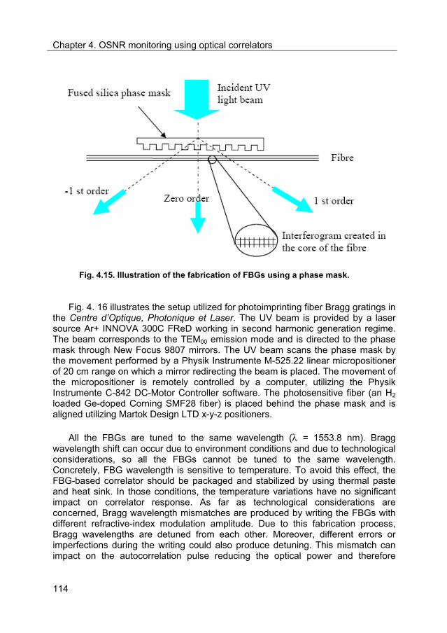
Chapter 4. OSNR monitoring using optical correlators
114
Fig. 4.15. Illustration of the fabrication of FBGs using a phase mask.
Fig. 4. 16 illustrates the setup utilized for photoimprinting fiber Bragg gratings in the Centre d’Optique, Photonique et Laser. The UV beam is provided by a laser source Ar+ INNOVA 300C FReD working in second harmonic generation regime. The beam corresponds to the TEM00 emission mode and is directed to the phase mask through New Focus 9807 mirrors. The UV beam scans the phase mask by the movement performed by a Physik Instrumente M-525.22 linear micropositioner of 20 cm range on which a mirror redirecting the beam is placed. The movement of the micropositioner is remotely controlled by a computer, utilizing the Physik Instrumente C-842 DC-Motor Controller software. The photosensitive fiber (an H2 loaded Ge-doped Corning SMF28 fiber) is placed behind the phase mask and is aligned utilizing Martok Design LTD x-y-z positioners.
All the FBGs are tuned to the same wavelength ( = 1553.8 nm). Bragg wavelength shift can occur due to environment conditions and due to technological considerations, so all the FBGs cannot be tuned to the same wavelength. Concretely, FBG wavelength is sensitive to temperature. To avoid this effect, the FBG-based correlator should be packaged and stabilized by using thermal paste and heat sink. In those conditions, the temperature variations have no significant impact on correlator response. As far as technological considerations are concerned, Bragg wavelength mismatches are produced by writing the FBGs with different refractive-index modulation amplitude. Due to this fabrication process, Bragg wavelengths are detuned from each other. Moreover, different errors or imperfections during the writing could also produce detuning. This mismatch can impact on the autocorrelation pulse reducing the optical power and therefore

Chapter 4. OSNR monitoring using optical correlators
115
increasing the monitor error. To overcome Bragg wavelength detuning, the FBG should be written with the same index modulation depth and the reflectivity can be adjusted by varying the FBG physical length as it is explained in [Fsa06b]. According to this requirement, the index modulation used in the correlator is set to
4105 .
Fig. 4. 16. Up: scheme of the experimental setup for photoimprinting fiber Bragg gratings. Down: graphic detail of the setup.

Chapter 4. OSNR monitoring using optical correlators
116
A FBG-based optical correlator is commonly constructed by using thermally controlled FBGs as tunable-reflectivity mirrors [Hau03]. The thermal control consists of a series of thin-film microheaters onto the surface of a single uniform grating which cause a shift in the grating spectrum towards longer wavelengths in response to the rise in temperature. Then, FBGs are fabricated to act as high reflectivity mirrors. By tuning the FBG thermally, the grating passband is shifted so that the signal wavelength intersects with the rising or falling edge of the grating response to obtain the desired reflectivities given by (4.11). However, tuning the grating reflectivity by operating it in the edge of the reflectivity is quite sensitive and has some disadvantages associated with polarization dependence, time-delay variation with reflectivity and dispersion. As each subgrating is tuned to a different reflectivity by operating them at the band edge, each grating will introduce some non-negligeable polarization dependent loss, causing distortion in the correlation output. Moreover, the time delay of a signal reflected from a FBG varies for different points along the edge. These unwanted time delay variations between subgratings degrades the correlation. Also, as the edge is steep, the signal can be affected by dispersion.
To solve these problems, the proposed correlator is also constructed by writing a series of uniform FBGs into a single length of fiber but each grating has the desired reflectivity thereby avoiding the thermal tuning and the inconvenience associated with operating at the edge of the FBG spectrum. Concretely, the reflectivities are fixed to 16%, 23%, 38% and 100% (using (4.11)). Fabricating low reflectivity gratings with high precision is not an easy task because of the reflectivity dependency on the tanh2(kL) function. This means that when the grating is not saturated, a slight deviation of the refractive index will have a large impact on the reflectivity. Fig. 4.17 shows the sensitive of the correlation to fabrication process when the reflectivity variations are ±10%. As it can be seen, these variations cause a slight reduction in the amplitude of the autocorrelation pulse.
Regarding the polarization dependence, Fig. 4.18 shows that the polarization dependence loss (PDL) of our correlator is almost zero in the FBG passband. The insertion loss and the PDL of the fabricated correlator were measured by means of the LUNA OVA CTe/STe device.

Chapter 4. OSNR monitoring using optical correlators
117
0 100 200 300 400 500 600
0.5
1
1.5
2
2.5
3
time(ps)
Cor
rela
tion
(a.u
.)
0 100 200 300 400 500 600
0.5
1
1.5
2
2.5
3
time(ps)
Cor
rela
tion
(a.u
.)
Fig. 4.17. Correlation output sensitivity to fabrication process.
1553 1553.4 1554 1554.4 1555 -25
-20
-15
-10
-5
0
5
10
Wavelength (nm)
(dB
)
PDL (dB)Insertion Loss (dB)
Fig. 4.18. Insertion loss and polarization dependence of our FBG-based correlator.

Chapter 4. OSNR monitoring using optical correlators
118
The fabrication process is as follows. The grating with the highest reflectivity, FBG4 (R4=100%), is firstly written. Then, the fiber is moved along its axis over a length corresponding to the required ‘0’ in the pattern and the FBG3 grating (R3=38%) is written. The FBG2 (R2=23%) and FBG1 (R1=16%) gratings are written following a similar process. The optical fiber length between the successive gratings are L1= 2.5810 mm, L2= 5.162 mm and L3= 10.324 mm, measured from the beginning of one grating to the beginning of the following one, as shown in Fig. 4.14. These lengths correspond to time intervals of Tb, 2Tb and 4Tb at 40 Gbit/s. The length of the gratings are LFBG1= LFBG2= LFBG3= 1 mm and LFBG4= 4 mm. The accuracy of the FBG positioning along the fiber is in the micrometer range. The bandwidth of the FBGs corresponds to a FWHM of 10 ps.
4.3.3. Characterization of the fabricated correlator
The first step to characterize the fabricated correlator is to launch one pulse into the correlator. In this case, four pulses with the same amplitude must appear at the correlator output. In addition, they must be spaced Tb, 2Tb, and 4Tb, which corresponds to 25 ps, 50 ps, and 100 ps for 40 Gbit/s operation. This behaviour can be confirmed in Fig. 4.19.
OutputOutput
Fig. 4.19. Characterization of the fabricated correlator by introducing one pulse into the correlator. (Time: 50ps/div)
Once characterized the correlator, the correlation functionality is validated by introducing the appropriate sequence into the correletor, i.e. Q= [10001011]. The correlator output for this sequence is shown in Fig. 4.20. As the incoming signal matches with the pattern stored in the array of FBGs, an autocorrelation pulse appears. The amplitude level of the sidelobes is almost the same at both sides of the autocorrelation pulse and some residual peaks appear at the end of the correlation function due to the secondary reflections produced inside the subgratings. These residual peaks suffer from larger time delays and attenuation.

Chapter 4. OSNR monitoring using optical correlators
119
Output
Input sequence Correlator response
1 1 1 10 00 0
Output
Input sequence Correlator response
1 1 1 10 00 0
Fig. 4.20. Correlator output for the incoming sequence Q= [10001011].
From Fig. 4.13 and Fig. 4.17 (simulation results), it can be noticed that the contrast between center peak and sidelobes is very high. In this case, the pulses remain phase correlated so that they are combined in field amplitude, as commented in the previous section. Concretely, the autocorrelation function is composed of 4 pulses (4E, where E is the field amplitude of one pulse). Then, in power magnitude, it corresponds to a contrast equal to 16P, where P is the pulse power. This result is in agreement with the contrast observed in Fig. 4.13 and Fig. 4.17. In contrast, in the experimental results the correlator was not sensitive to the coherence issues and the pulses were incoherently combined. This is the consequence of incoherent operation of output laser pulses. From Fig. 4.20, it can be seen that the autocorrelation pulse is almost four times the sidelobes which corresponds to considering autocorrelation function in power basis (the contrast is approximately 3.7). Moreover, as it has been mentioned before, the spacings between gratings were carefully chosen to avoid that the autocorrelation pulse was combined with multiple reflected pulses so that the autocorrelation function was less sensitive to coherence time effects. In particular, unequal spacing between gratings was used. This solution was pointed out in [Fsa06b].
4.4. Experimental validation of the OSNR monitoring technique
After the characterization of the fabricated correlator, experimental demonstration of the monitoring system is carried out in the laboratory as a proof-of-concept.
The principle of operation of the OSNR monitoring technique is validated experimentally by means of the setup shown in Fig. 4.21.

Chapter 4. OSNR monitoring using optical correlators
120
FMLL
40 GHz RZ pulses
OBF
BW= 0.4 nm
ODLOVA PC
MZM
EDFA
Circulator
Scope
ASEsource
PRBS
R1
FBG1FBG2FBG3
R3 R2
L1L3 L2
R4
FBG4
OSNR Monitor
OBF
OBF
To Optical Spectrum Analyzer
FMLL
40 GHz RZ pulses
OBF
BW= 0.4 nm
ODLOVA PC
MZM
EDFA
Circulator
Scope
ASEsource
PRBS
R1
FBG1FBG2FBG3
R3 R2
L1L3 L2
R4
FBG4
OSNR Monitor
OBF
OBF
To Optical Spectrum Analyzer
Fig. 4.21. Experimental setup
The monitoring-field, Q = [10001011], is generated through external modulation of an RZ Gaussian pulse source at 1553.8 nm. The modulating signal driving the Mach-Zehnder modulator (MZM) is obtained from a 40 Gbit/s electrical PRBS equipment. The signal out from the transmitter is coupled with a second EDFA to simulate the link noise. Thus, the OSNR of the optical signal can be changed by combining the signal with different ASE noise levels adjusting the gain of the EDFA pump laser. The response of the EDFA for different gain values is shown in Fig. 4.22. The optical signal degraded with the noise passes through a 1-nm bandwidth filter and then is split in two branches for OSNR measurements. One branch uses an optical spectrum analyzer (OSA) as reference and the other branch goes to the OSNR monitor. Inside the OSNR monitor, an optical circulator is placed at the array input to route the counter-propagating correlation output to the sampling scope.

Chapter 4. OSNR monitoring using optical correlators
121
1510 1520 1530 1540 1550 1560 1570 1580 1590-55
-50
-45
-40
-35
-30
-25
-20
-15
-10
-5
Wavelength (nm)
Po
we
r (d
Bm
/nm
)
EDFA response
G=16%G=40%G=70%G=100%
Fig. 4.22. EDFA response for different gain values (ASE noise source).
The optical correlator output is sensitive to the fluctuations in the received signal due to the fiber impairments and it can be used to estimate the OSNR of the optical packets from the statistics of the autocorrelation pulse, as shown in the Fig. 4.23. Concretely, by using the mean value and the standard deviation, the OSNR value is calculated. These values are extracted by means of a high-speed sampling scope. Despite using a sampling scope, the technique allows high-speed bitrate operation as it only measures the autocorrelation pulse, so the system works at the packet rate and thereby alleviating speed requirements with respect to typical BER techniques, as it was mentioned in previous sections.

Chapter 4. OSNR monitoring using optical correlators
122
Fig. 4.23. Noise statistics of the autocorrelation pulse.
To demonstrate the feasibility of the proposed OSNR monitoring technique, the OSNR from OSA is measured and compared with the value extracted from the noise statistics from the autocorrelation pulse. This reference OSNR (i.e. OSNR from OSA) is calculated as follows:
ASE
S
P
POSNR , (4.17)
where PS is the signal peak power and PASE is the ASE noise floor level for the channel bandwidth. Fig. 4.24 depicts the measured OSNR from the autocorrelation pulse using the proposed technique as a function of the actual OSNR measured by the OSA. As it can be seen, the estimated OSNR values agree well with the results extracted from the OSA.

Chapter 4. OSNR monitoring using optical correlators
123
15 16 17 18 19 20 21 22 23 24 25
16
18
20
22
24
OSNR with OSA (dB)
Cor
rela
tor
Out
put O
SN
R (
dB)
-0.5
0
0.5
Mon
itorin
gE
rror
(dB
)
15 16 17 18 19 20 21 22 23 24 25
16
18
20
22
24
OSNR with OSA (dB)
Cor
rela
tor
Out
put O
SN
R (
dB)
-0.5
0
0.5
Mon
itorin
gE
rror
(dB
)
15 16 17 18 19 20 21 22 23 24 25
16
18
20
22
24
OSNR with OSA (dB)
Cor
rela
tor
Out
put O
SN
R (
dB)
-0.5
0
0.5
Mon
itorin
gE
rror
(dB
)
15 16 17 18 19 20 21 22 23 24 25
16
18
20
22
24
OSNR with OSA (dB)
Cor
rela
tor
Out
put O
SN
R (
dB)
-0.5
0
0.5
Mon
itorin
gE
rror
(dB
)
Fig. 4.24. OSNR monitoring: OSNR measured using an OSA and using the proposed technique.
The OSNR monitoring errors are the difference between the OSNR measured from the OSA and from the autocorrelation output pulse. From the curve the maximum error for the measurement of different OSNR values is 0.5 dB in the 15 dB to 25 dB OSNR range (Fig. 4.24). The slight deviation in lower OSNR values can be explained by the noise filtering behavior of the FBG-based correlator. The optical signal degraded with the noise passes through a 1-nm bandwidth filter and enters the optical correlator whose bandwidth is approximately 0.6-nm. Therefore, for lower OSNR values the output of the correlator is less sensitive to the degradation than the input, primarily due to the narrower optical passband of the FBG-based correlator providing a smaller noise background. Conversely, for higher OSNR values, where the noise background is practically negligible, the difference is due to the insertion loss of the gratings which slightly affects the power of the correlator response. Therefore, monitoring errors are caused by noise at lower OSNR values and by insertion loss at higher OSNR values.

Chapter 4. OSNR monitoring using optical correlators
124
4.5. Applications of the proposed OSNR monitoring technique
Apart from the monitoring function itself, the monitoring system has other useful applications. The main field of application is the signal quality characterization for quality of service (QoS) implementation. Furthermore, the monitoring information can be used to establish new optical paths based on quality requirements or select backup paths when recovery mechanisms are needed. Next, these applications are explained in more detail.
4.5.1. Monitoring for QoS implementation
With the introduction of new generation multimedia services, OPS networks transport different types of traffic with different quality requirements so that performance monitoring is especially important to ensure that packets receive appropriate treatment as they travel through the network. Packets entering the network must be analyzed to determine their QoS requirements depending on the kind of network service and then the signal quality must be monitored in each intermediate node to guarantee certain level of performance.
In this scenario, the monitoring-field (i.e. Q) inserted into the packet header for monitoring functions specifies the QoS requirement of the incoming packet. In other words, this QoS field fixes the quality of signal requirements for each packet flow coming from a specific service. Optical headers of packets with the same QoS requirements, i.e. the same monitoring-field associated with the same kind of service, are then processed in each intermediate node to check if the estimated quality fulfils the terms of QoS and to guarantee the required level of performance. Fig. 4.25 shows the block diagram of the proposed monitor as a part of the QoS implementation [Vil07].
The monitor is composed of M correlators, each of which is configured to produce a “match” signal for a specific QoS. The number of correlators, M, defines the number of type of services or QoS levels provided by the carriers. The correlator is composed of a series of gratings written into a fiber whose principle of operation is similar to the FBG-based correlator explained in this Chapter.

Chapter 4. OSNR monitoring using optical correlators
125
Header Q1
Monitoring-fieldextraction
Optical correlator 1 Autocorrelation pulse
OSNR estimated
1xM
Q1
Q1
Q2
QM
Optical correlator 2
Optical correlator M
Header Q1
Monitoring-fieldextraction
Optical correlator 1 Autocorrelation pulse
OSNR estimated
1xM
Q1
Q1
Q2
QM
Optical correlator 2
Optical correlator M
Fig. 4.25. Block diagram of the OSNR monitor for QoS implementation
Three basic levels are normally defined in the network: best-effort service, differentiated service and guaranteed service [Int03], each of which is defined by a different monitoring-field (i.e. Q1 for best-effort, Q2 for differentiated, and Q3 for guarantee). Thanks to the definition of different Q values, each intermediate node can monitor packet flows with the same QoS requirement independently since the autocorrelation peak activates the OSNR process. In other words, the output of the correlator is compared with a defined threshold so that when the amplitude of the autocorrelation pulse exceeds the threshold level, the monitoring process is activated. Then, from the OSNR value estimated with the correlator, each intermediate node can control whether the transmission meets the QoS and performance requirements specified by the carrier, providing a consistent treatment for each QoS class at every hop. Fig. 4.26 shows the correlator output for three QoS levels. Only in the case where the input signal matches the pattern written into the fiber, an autocorrelation pulse appears and the OSNR monitor is activated. Otherwise, the peak decreases and the OSNR monitoring for the corresponding Q values is inhibited. As commented previously, the definition of different Q values allows the network to offer differentiated services with specific quality requirements. Although no standards for the quality parameters have been defined yet, BER degradation is usually considered as the parameter to be monitored as some applications may tolerate degraded BER and others will not. In case of guaranteed service, the BER value should be lower than 10-12. In case of differentiated service, some BER degradation is allowed and the BER values vary between 10-12 and 10-
6. Finally, best-effort service establishes the connectivity with no guarantees so the required BER is not too strict. The corresponding OSNRs for each service depend on the optical receiver. For example, for a typical optical system a BER < 10-12 corresponds to an OSNR value higher than 20 dB [Cisco].
In addition, the proposed monitoring system can be integrated with other functions in the packet switching node to take immediate actions when the signal quality is strongly degraded. The beauty of using performance monitors close to the intermediate switching nodes is that the monitored parameters can be associated with the switch controls and label information. Therefore it is possible to

Chapter 4. OSNR monitoring using optical correlators
126
integrate the optical performance monitors with switching nodes for providing network intelligence and fast impairment mitigation.
OpticalNetwork
Best-effort
Differentiated
Guaranteed
Data
Voice
Multimedia
Q1
Q2
Q3
1
Output
Output
Output
a)
b)
c)
1
1
1 1
1
1
1
1
1 0 00
0
0
0
00 0
0 0
0 0 1
Q1
Q2
Q3
OpticalNetwork
Best-effort
Differentiated
Guaranteed
Data
Voice
Multimedia
Q1
Q2
Q3
1
Output
Output
Output
a)
b)
c)
1
1
1 1
1
1
1
1
1 0 00
0
0
0
00 0
0 0
0 0 1
Q1
Q2
Q3
1
Output
Output
Output
a)
b)
c)
1
1
1 1
1
1
1
1
1 0 00
0
0
0
00 0
0 0
0 0 1
Q1
Q2
Q3
Fig. 4.26. Independent treatment for each QoS class in the intermediate nodes by means of the use of an optical correlator.
4.5.2. Monitoring for OSNR-assisted routing
The combination of the increasing demand for capacity and the trend towards OPS networks creates new challenges to QoS provisioning. In this fully reconfigurable scenario, the optical packets are no longer regenerated in the networks nodes and the changing nature of the traffic demand requires dynamic path computation taking into account the impact of physical impairments on the feasibility of the lightpaths [Kil02]. Therefore, a solution for the integration of the control plane and OPM functions must be implemented. In this context the monitoring information obtained from the optical correlator could assist the routing system which interacts

Chapter 4. OSNR monitoring using optical correlators
127
with the control plane to contribute to the supervision of service level agreement (SLA) fulfilment and efficiently perform routing based on signal quality requirements. Fig. 4.27 shows the proposed interaction between the control plane and the monitoring system. The monitoring system is based on the OSNR monitor presented in this Chapter, but instead of processing a specific word, Q, inserted into the packet header, a set of test packets are periodically sent along the network following different paths (e.g. paths P1, P2, P3, and P4 shown in Fig. 4.27). These packets are processed in each intermediate node to monitor the network performance.
A
C
E
D
F
P1
P2
P3
P4
BAutocorrelation
pulse
OSNR Monitoring
Monitoring ModuleQ
Control Plane
Opticalcorrelator
Best OpticalPath Decision
A
C
E
D
F
P1
P2
P3
P4
BAutocorrelation
pulse
OSNR Monitoring
Monitoring ModuleQ
Control Plane
Opticalcorrelator
Best OpticalPath Decision
Fig. 4.27. Interaction between the proposed monitoring system and the control plane
The link performance information coming from this monitor is then disseminated by the control plane and shared between network nodes to assess the status of all connections. Moreover, the OSNR estimation is added as an additional factor in the routing decision. Then, every link, i, is characterized by a parameter i which includes the signal quality estimated. Since the impairments are additive, the quality degradation of a path is determined by the sum of the i of the traversed links. A maximum value MAX associated with QoS requirements is defined. For a dynamic path setup, the control plane investigates the value of this monitoring parameter to calculate potential routes. Among them, lightpaths whose accumulate physical impairments do not exceed MAX are possible candidate while the others are no longer considered. Finally, one of these feasible routes is selected. Therefore, this OSNR-assisted routing allows the control plane to establish or select lightpaths taking into account physical impairments and thereby sustaining reliability requirements and keeping the level of quality of service promised to end users.

Chapter 4. OSNR monitoring using optical correlators
128
4.5.3. Path monitoring for restoration functions
As it has been mentioned, the monitoring information obtained by the OSNR monitor can be used for assisting the routing system in order to establish new optical paths based on quality requirements. Apart from this application, the extracted quality parameter could be used by the fault management system to start the recovery mechanisms and also to establish backup paths taking into account performance requirements.
The proposed signal quality monitoring system is based on periodically sending test packets over a supervisory wavelength. The supervisory wavelength is reserved in each link between two adjacent nodes to transmit the test packet, allowing failure detection immediately when the node does not receive any signal. When a failure occurs, the node reports this fault condition to the control plane to start the recovery actions. These packets are processed by the FBG-based correlator in the end nodes to assess the quality of a set of backup paths. Then, the network state is inferred from the result of a set of end-to-end measurements, providing a cost-effective recovery solution. For restoration to be feasible, disjoint backup paths are defined, concept widely used for the design of a survivable WDM optical network because it may be faster, simpler and easier than other restoration techniques [Kod03].
Fig. 4.28 shows the principle of operation of the proposed monitoring system. In this figure, some packets are transported over the working paths P1 and P2, and two disjoint backup paths (dashed lines) which do not share the same links are also defined. The test packets transmitted over each of these backup paths are labelled with a specific data word, B1 and B2, defined in a similar way to the monitoring-field used in the OSNR monitoring technique. Then, the test packets are processed in the destination node to monitor the quality of these backup paths by means of a bank of optical correlators. As in the case of the QoS implementation, each correlator is configured to monitor a specific backup path.

Chapter 4. OSNR monitoring using optical correlators
129
A
C
E
D
B
F
λ
λ supervisorydata data
P1
P2
B2
B1
End node
1xMAutocorrelation pulse
OSNR Monitoring
B1
B2
BM
Opticalcorrelator 1
Opticalcorrelator 2
Opticalcorrelator M
A
C
E
D
B
F
λ
λ supervisorydata data
P1
P2
B2
B1
End node
1xMAutocorrelation pulse
OSNR Monitoring
B1
B2
BM
Opticalcorrelator 1
Opticalcorrelator 2
Opticalcorrelator M
Fig. 4.28. Path monitoring system for restoration functions.
With this solution the fault management system is able to detect transmission failures, start recovery mechanism, and monitor the network performance in a cost-effective way.
4.6. Summary and conclusions
As other networks, optical impairments degrade the performance of OPS networks and, therefore, monitoring optical signal quality is becoming critically important. In fact, OSNR monitoring is essential for signal quality management in such networks.
Unlike circuit switching, OPS technology routes optical packets over independent paths to their destination so that each packet suffers from different level of degradation. As a result, OPS networks require new technologies to perform OSNR monitoring with fast response directly at the optical physical layer.
In this Chapter, a novel OSNR monitoring technique based on optical correlation has been proposed and demonstrated experimentally. To this end, a specific monitoring field is inserted into the optical label and is processed in each intermediate node. The monitoring system is composed of a circuit responsible of extracting the monitoring field and the monitor itself based on a FBG-based correlator. Along this Chapter, the principle of operation of the OSNR monitoring technique has been described and the basis of the FBG-based correlator has been presented. Simulations have been carried out to properly design the parameters of the correlator. After characterization of this device, the monitoring technique has been experimentally demonstrated. By measuring the noise statistics of the autocorrelation pulse peak power, the OSNR has been estimated with an error

Chapter 4. OSNR monitoring using optical correlators
130
lower than 0.5 dB. Thereby the autocorrelation peak can be a feasible indicator of the signal impairments in high-speed optical networks.
The advantages of the proposed OSNR monitoring technique are the following:
The technique provides in-band measurements. It eliminates the extrapolation uncertainty using the out-band approach.
The technique performs the signal quality monitoring with relaxed speed requirements with respect to typical techniques as the correlator works at the packet rate.
The FBG-based correlator is easily manufactured.
The technique offers the possibility of integration with other functions in the packet switching node to take immediate actions when the signal is strongly degraded.
Furthermore, some practical applications of the proposed OSNR monitor have been presented. First, the OSNR monitor could be deployed as part of QoS to ensure that packets are properly treated along the network according to their QoS level. Second, the monitoring information obtained from the optical monitor could be included when calculating new routes for data signals. Indeed, signal quality monitoring information could be added as an additional factor in the routing decision. Finally, the OSNR information could also be utilized for path monitoring for restoration functions.

Chapter 4. OSNR monitoring using optical correlators
131
4.7. References
[And93] D.Z. Anderson, V. Mizrahi, T. Erdogan, and A.E. White, “Production of in-fiber gratings using a diffractive element,” Electron. Lett., vol. 29, no. 6, pp. 566–568, 1993.
[Blu00] D.J. Blumenthal, B.E. Olsson, G. Rossi, T.E. Dimmick, L. Rau, M. Masanovic, O. Lavrova, R. Doshi, O. Jerphagnon, J.E. Bowers, V. Kaman, L.A. Coldren, and J. Barton, “All-optical label swapping networks and technologies”, IEEE/OSA J. Lightwave Technol., vol. 18, no. 12, pp. 2058-2075, 2000.
[Bou08] N. Boudriga1, A. Lazzez, Y. Khlifi, and M. Zghal2, “All Optical Network Switching: A New Scheme for QoS Provision and Virtual Memory Control,” in Porc. of 10th International Conference on Transparent Optical Networks (ICTON’08), Athens (Greece), paper We.B3.3, 2008.
[Chan77] C.T. Chang, J.A. Cassaboom, and H.F. Taylor, “Fibre-optic delay-line devices for R. F. signal processing”, Electron. Lett., vol. 13, no. 22, pp. 678–680, 1977.
[Cisco] Data sheet: “OC-192/STM-64 Line Card Portfolio for the Cisco ONS 15454 SONET/SDH Multiservice Provisioning Platforms”.
[Ding04] L. Ding, W.D. Zhong, C.Lu, and Y. Wang, “A new bit error rate monitoring method based on histograms and curve fitting”, Opt. Express., vol. 12, no. 11, pp. 2507–2511, 2004.
[Erd97] T. Erdogan, “Fiber grating spectra”, IEEE/OSA J. Lightwave Technol., vol. 15, no. 1, pp. 1277–1294, 1997.
[Eul83] G.W. Euliss and R.A. Athale, “Time-integrated correlator based on fiber-optic delay lines”, Opt. Letters, vol. 43, pp. 149–151, 1983.
[Eul94] G.W. Euliss and R.A. Athale, “Time-integrating correlator based on fiber-optic delay lines”, Opt. Letters, vol. 19, pp. 649–651, 1994.
[Fsa06a] I. Fsaifes, C. Lepers, M. Lourdiane, R. Gabet, and P. Gallion, “Pulsed laser source coherence time impairments in a direct detection DS-OCDMA system,” in Proc. of Conf. Lasers Electro-optics (CLEO’06), Long Beach (CA, USA), paper CWH6, 2006.
[Fsa06b] I. Fsaifes, C. Lepers, A. Obaton, and P. Gallion, “DS-OCDMA encoder/ decoder performance analysis using optical low-coherence reflectometry,” IEEE/OSA J. Lightwave Technol., vol. 24, no. 8, pp. 3121–3128, 2006.
[Han90] D.P. Hand, and P.S.J. Russell, “Photoinduced refractive-index changes in germano silicate fibers,” Opt. Letters, vol. 15, no. 2, pp. 102–104, 1990.

Chapter 4. OSNR monitoring using optical correlators
132
[Hau03] M.C. Hauer, J.E. McGeehan, S. Kumar, J.D. Touch, J. Bannister, E.R. Lyons, C.H. Lin, A.A. Au, H.P. Lee, D.S. Starodubov, and A.E. Willner, “Optically assisted internet routing using arrays of novel dynamically reconfigurable FBG-based correlators,” IEEE/OSA J. Lightwave Technol., vol. 21, no. 11, pp. 2765–2778, 2003.
[Hill97] K. Hill, and G. Meltz, “Fiber Bragg grating technology fundamentals and overview,” IEEE/OSA J. Lightwave Technol., vol. 15, no. 8, pp. 1263–1276, 1997.
[Jac85] K.P. Jackson, S.A. Newton, B. Moslehi, M. Tur, C.C. Cutler, J.W. Goodman, and H.J. Shaw, “Optical fiber delay-line signal processing,” IEEE Trans. Microwave Theory Tech. MTT-33, pp. 193–209, 1985.
[Int03] “Internetworking Technologies Handbook,” Indianapolis, IN: Cisco Systems, Inc. Cisco Press, 2003.
[Kas99] R. Kashyap, “Fiber Bragg Gratings,” Academic Press, London, 1999.
[Kil02] D.C. Kilper, et al., “Optical Performance Monitoring,” IEEE/OSA J. Lightwave Technol., vol. 22, no. 1, pp. 294-304, 2002.
[Kil04] D.C. Kilper, A. Azarov, W. Weingartner, and P. Vorreau, “Q-factor monitoring for fault management applications,” in Proc. of Optical Fiber Communication Conference (OFC’04), Los Angeles (CA, USA), vol. 2, p. 3, 2004.
[Kod03] M. Kodialam, “Dynamic Routing of restorable bandwidth-guaranteed tunnels using aggregated network resource usage information,” IEEE/ACM Transaction on networking, vol. 11, pp. 399-410, 2003.
[Kog76] H. Kogelnik, “Filter response of nonuniform almost-periodic structures,” Bell System Technical Journal, vol. 55, pp. 109–126, 1976.
[Koy07] K. Koyama, J.I. Hashimoto, Y. Tsuji, T. Ishizuka, and T. Katsuyama, “Optical label Encoder/Correlator on GaAs-based photonic integrated circuit for photonic networks,” Sei Technical Review, no. 65, pp. 11-14, 2007.
[Lem93] P.J. Lemaire, R.M. Atkins, V. Mizrahi, and W.A. Reed, “High pressure H2 loading as a technique for achieving ultrahigh UV photosensitivity and thermal sensitivity in GeO2 doped optical fibres,” Electron. Lett., vol. 29, no. 13, pp. 1191–1193, 1993.
[Mel89] G. Meltz, W.W. Morey, and W.H. Glenn, “Formation of Bragg gratings in optical fibers by a transverse holographic method,” Opt. Letters, vol. 14, no. 15, pp. 823–825, 1989.
[Mob05] E. Mobilon, “Experimental verification of an eye diagram reconstruction technique based on asynchronous undersampling”, IEEE MTT-S, pp. 603-606,

Chapter 4. OSNR monitoring using optical correlators
133
2005.
[Oth99] A. Othonos, K. Kalli, “Fiber Bragg Gratings: Fundamentals and Applications inTelecommunications and Sensing,” Artech House, Norwood, MA, 1999.
[Pet01] P. Petropoulos, N. Wada, P.C. The, M. Ibsen, W. Chojo, K.I. Kitayama, and D.J. Richardson, “Demonstration of a 64-chip OCDMA system using superstructured fiber gratings and time-gating detection,” IEEE Photonics Technology Letters, vol.13, no. 11, pp.1239-1241, 2001.
[Sha98] I. Shake, H. Takara, S. Kawanishi, and Y. Yamabayashi, “Optical signal quality monitoring method based on optical sampling,” Electron. Lett., vol. 34, no. 22, pp. 2152-2154, 1998.
[Sha03] I. Shake, H. Takara, and S. Kawanishi, “Simple Q factor monitoring for BER estimation using opened eye diagrams captured by high-speed asynchronous electrooptical sampling,” IEEE Photon. Technol. Lett., vol. 15, no. 4, pp. 620–622, 2003.
[Tak02] K. Takiguchi, T. Shibata, and M. Itoh, “Encoder/decoder on planar lightwave circuit for time-spreading/wavelength-hoping optical CDMA,” Electron. Lett., vol. 38, no. 10, pp. 469–470, 2002.
[Vil07] R. Vilar, F. Ramos, and J. Marti, “Optical signal quality monitoring using fibre-Bragg-grating-based correlators in optical packet-switched networks,” in Proc. of 33rd Eur. Conf. Opt. Commun. (ECOC’07), Berlin (Germany), vol. 5, pp. 239–240, 2006.
[Wen05] Y.G. Wen, and V.W.S. Chan, “Ultra-reliable communication over vulnerable all-optical networks via lightpath diversity,” IEEE J. Selected Areas in Communications, vol. 23, no. 8, pp. 1572–1587, 2005.
[Yam87] M. Yamada, and K. Sakuda, “Analysis of almost-periodic distributed feed-back slab waveguide via a fundamental matrix approach,” Applied Optics, vol. 26, no. 16, pp. 3474–3478, 1987.
[Yar73] A. Yariv, “Couple-mode theory for guided-wave optics,” IEEE Journal of Quantum Electronics, vol. 9, no. 9, pp. 919–933, 1973.
[Ye07] D. Ye, and W.D. Zhong, “Improved BER monitoring based on amplitude histogram and multi-Gaussian curve fitting,” J. Optical Networking, vol. 6, pp. 584–598, 2007.

135
Chapter 5
PMD monitoring using XOR gate
5.1. Introduction
Optical packet switching (OPS) technology is particularly attractive as a possible technology for future telecommunication networks. Despite this promising perspective, the technical process of achieving OPS networks requires the successive removal of technical barriers. In fact, Polarization Mode Dispersion (PMD) is considered one of the most important sources of transmission degradation, strongly limiting the performance of such next generation networks [Sun02].
PMD is a consequence of the random optical birefringence along the fiber. In first order, it causes an optical signal to decompose into two polarization states travelling with different propagation velocities and thus arriving at different times at the receiver. This difference in arrival time is described by the Differential Group Delay (DGD). This effect generates major signal distortion as the bitrate is increased. So with the trend towards ultrahigh bitrates, PMD phenomena bring about new challenges to the deployment of transmission systems at 40 Gbit/s and beyond due to its statistical nature over time and its dependence on temperature variations [Bul00]. Therefore, it is important to find convenient way to monitor these effects in real-time and to dynamically adapt optical or electronic equalisation/mitigation elements [Wil04].

Chapter 5. PMD monitoring using XOR gate
136
In the literature some techniques based on electrical power spectrum measurements of the detected signal have been proposed for dynamic PMD monitoring [Tak94, Noe99, Pua00]. However, as signals get faster it is becoming harder to use traditional electrical measurements and a true monitoring of the high-speed optical signal is not possible. Monitoring at the optical domain is a promising solution due to its simplicity, scalability and ‘‘on-the-fly” processing capability. All-optical monitors based on the frequency resolved state-of-polarization (FRSOP) method [Bos02] and the degree-of-polarization (DOP) technique [Lan02] have been proposed, but these approaches are not appropriate for high-speed OPS networks because of the slow response of the FRSOP method and the low reliability of the DOP technique when the DGD becomes large. As the optical paths change continuously, different packets can arrive at the node with different DGD values, so real-time DGD packet monitoring is a relevant challenge.
In this Chapter, an all-optical technique for first-order PMD monitoring in OPS networks is proposed. The technique is based on the use of an optical logic XOR gate implemented by an integrated SOA-based Mach–Zehnder interferometer (SOA-MZI) for PMD estimation. Moreover, the output of the XOR gate can act as the control signal for an all-optical 1x2 packet switch, allowing the node taking real-time decisions about packet routing according to the estimated DGD values.
The principle of operation of the whole monitoring system is described in Section 2 where the use of optical logic gates (i.e. SOA-MZI in different configurations) to integrate DGD monitor with switching nodes for providing network intelligence is emphasized. The simulation results presented in Section 3 show successful operation of the architecture. Such operation is confirmed with the experimental validation of the XOR-based monitoring subsystem stated in Section 4. Section 5 gathers the conclusions derived from the work presented in this Chapter.
5.2. Principle of operation
PMD strongly limits the performance of long-haul optical links and next generation networks including OPS networks. Optical packets are forwarded hop-by-hop based on optical packet header information and packet forwarding table at each switching node [Blu00]. In such an OPS network, an optical packet may traverse a number of optical packet switching nodes following its own optical path along the network. Since the label and the payload travel along the same path, there will be a correlation between DGD of the label and payload. This allows a simple method to optically monitor the DGD of a packet without affecting its performance.
Following this idea, the proposed monitoring system is based on using the packet label to infer the PMD value of the incoming packet. When the packet arrives at the node, the label is extracted and processed in the node for monitoring

Chapter 5. PMD monitoring using XOR gate
137
purposes, similar to the way explained in Chapter 3. Then, the two orthogonal polarization states of the label are compared by using an optical logic XOR gate implemented by an SOA-MZI for PMD estimation. After the XOR operation, the output of this optical logic gate acts as the control signal for an all-optical 1x2 packet switch so that depending on the estimated PMD, the optical packet can be sent to a real-time, per-packet-basis PMD compensator or dropped if it is strongly degraded. The all-optical 1x2 packet switch is also based on a SOA-MZI, but in optical flip-flop operation as it will be explained later.
The main subsystems comprising the all-optical DGD packet monitor are shown in Fig. 5.1.
Payload Label
Label
1x2 Switch
Switch Control
Payload
Drop port
Regeneration port
Label extraction
XOR-basedDGD Monitoring
DGD monitor
Payload Label
Label
1x2 Switch
Switch Control
Payload
Drop port
Regeneration port
Label extraction
XOR-basedDGD Monitoring
DGD monitor
Fig. 5.1. Block diagram of the proposed DGD monitoring system.
Then, when the packet enters the packet switching node, a part of the input optical signal power is tapped and fed into the DGD monitor. Inside the DGD monitor, the label is extracted from the payload and then sent to the DGD monitoring block itself. This block estimates the DGD value for the input label and generates the appropriate control signal to feed the 1x2 latching switch.
5.2.1. XOR-based DGD Monitoring
The key component in this system is the XOR-based DGD monitor. The preferred architecture for performing logic operations is based on interferometric structures which often incorporate a nonlinear element in some of its two branches or in both. This nonlinear element adjusts the phase of the signal passing through it to perform the logic operation. The proposed DGD monitor is implemented by an integrated SOA-MZI [Mas03, Pat05, Pou06]. This interferometer is comprised of

Chapter 5. PMD monitoring using XOR gate
138
two branches in which a SOA is placed. In a basic operation the SOA acts as a nonlinear element, inducing an additional phase change.
The proposed architecture for the XOR-based DGD monitor is shown in Fig. 5.2.
SOA
SOA
Integrated SOA-MZI
Control
XOR
# 1
# 2
# 3
# 4
CW
Switch Control
PBS
TE
TM
LabelSOA
SOA
Integrated SOA-MZI
Control
XOR
# 1
# 2
# 3
# 4
CW
Switch Control
PBS
TE
TM
Label
Fig. 5.2. XOR-based DGD monitor.
The input label splits in two orthogonal polarization modes (TE and TM) using a polarization beam splitter (PBS). Then both signals are compared by means of the logic XOR gate, so delay differences between both polarizations can be detected [Ito02]. The SOA-MZI performs the XOR operation between the two data signals coupled into ports #1 and #3. To this end, a continuous wave light acting as a control signal must be injected through port #4.
In the MZI, both data signals are launched into the SOAs where their carrier densities and thereby the refractive index are modulated. This causes a phase modulation of the control signal propagating through the SOAs according to the intensity variations of the input data signals (cross-phase modulation).
By properly setting the input optical powers and controlling the SOA parameters, the control signal from the two SOAs interferes either constructively or destructively at the output of the interferometer in order to provide the logical XOR operation of the two data sequences [Fje00, Kim02, Mar06]. The output intensity is proportional to
2sin 312
I , (5.1)

Chapter 5. PMD monitoring using XOR gate
139
where 1 and 3 are the phase changes introduced to the control signal over
the upper and lower branches.
In the case in which both input data are the same, data pulses reach both SOAs, and the phase shift induced to the control signal in each branch is the same. As a result, at port #2 no signal is obtained due to the destructive interference between the input signals. Conversely, when there is input signal in only one port, the refractive index of one branch changes whereas the other one remains unaffected. Then, at port #2, the control signal from the two SOAs is combined and an optical pulse is obtained as a consequence of the constructive interference.
According to the XOR operation, when both data signals (TE and TM modes) are time synchronized (DGD = 0), no pulses are obtained at the SOA-MZI output (port #2). Conversely, as the data signals give up time overlapping (DGD ≠ 0), some pulses with increasing energy will appear at the SOA-MZI output (Fig. 5.3). So this output signal may show a measure of the DGD, and it is then used to feed an optical switch to decide about regenerating/routing or dropping the packet.
Input signal
Differential Group Delay
TM
TE
DGD = 0 DGD ≠ 0
Input signal
Differential Group Delay
TM
TE
DGD = 0 DGD ≠ 0
Fig. 5.3. Conceptual basis of the XOR-based DGD monitoring.
5.2.2. Optical packet switch
The optical packet switch is also based on a SOA-MZI structure with a feedback loop operating in a similar way to an optical flip-flop [Cla05, Cla06]. The principle of operation for this latching circuit is described as follows.
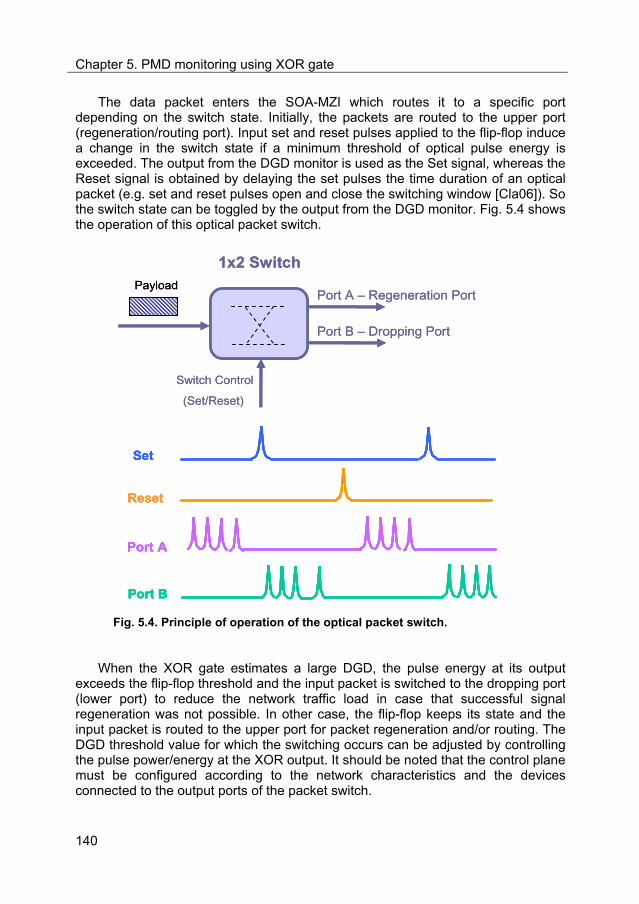
Chapter 5. PMD monitoring using XOR gate
140
The data packet enters the SOA-MZI which routes it to a specific port depending on the switch state. Initially, the packets are routed to the upper port (regeneration/routing port). Input set and reset pulses applied to the flip-flop induce a change in the switch state if a minimum threshold of optical pulse energy is exceeded. The output from the DGD monitor is used as the Set signal, whereas the Reset signal is obtained by delaying the set pulses the time duration of an optical packet (e.g. set and reset pulses open and close the switching window [Cla06]). So the switch state can be toggled by the output from the DGD monitor. Fig. 5.4 shows the operation of this optical packet switch.
1x2 Switch
Switch Control
(Set/Reset)
Port B – Dropping Port
Port A – Regeneration PortPayload
Set
Reset
Port B
Port A
1x2 Switch
Switch Control
(Set/Reset)
Port B – Dropping Port
Port A – Regeneration PortPayload
Set
Reset
Port B
Port A
Set
Reset
Port BPort B
Port APort A
Fig. 5.4. Principle of operation of the optical packet switch.
When the XOR gate estimates a large DGD, the pulse energy at its output exceeds the flip-flop threshold and the input packet is switched to the dropping port (lower port) to reduce the network traffic load in case that successful signal regeneration was not possible. In other case, the flip-flop keeps its state and the input packet is routed to the upper port for packet regeneration and/or routing. The DGD threshold value for which the switching occurs can be adjusted by controlling the pulse power/energy at the XOR output. It should be noted that the control plane must be configured according to the network characteristics and the devices connected to the output ports of the packet switch.

Chapter 5. PMD monitoring using XOR gate
141
5.3. Simulation results
The proposed DGD monitoring system is tested by means of simulations using the Virtual Photonics Inc. software, VPI.7.1. The objective of the simulations is the evaluation of the whole system to demonstrate the principle of operation employing realistic specifications of commercially available devices such as SOA-MZI parameters, optical powers of laser sources, etc. The schematic under study considers an optical XOR gate based on a SOA-MZI whose output acts as the control signal for the optical packet switch.
The input packets at 1556 nm are generated by externally modulating at 40 Gbit/s an RZ gaussian pulse source. The input label is encoded by phase modulating an 8-bit sequence at 10 Gbit/s (FWHM = 10 ps). The reason for using phase-modulated labels is that a pulse train is required to monitor the DGD. So intensity-modulated labels cannot be used unless a sequence [1 1 1 1 1 ….] is appended to the label. Typical optical packet networks are based on the use of low bitrate optical labels. The main reason of using a bitrate lower than the packet is that the processing of such labels is mainly limited by technological reasons. In fact, the performance of the XOR-based DGD monitor is very dependent on the operation speed. Bitrates up to 10 Gbit/s are easily handled by current SOA-MZI technology, but for bitrates of 40 Gbit/s and beyond, the performance is reduced and the implementation of alternative techniques, such as the differential scheme approach [Che02], is required. The XOR gate with a differential scheme will be discussed in next sections.
The data peak power is adjusted at 1 mW at the input of the optical switch whereas the label peak power is 10 mW. To emulate the PMD waveform distortion, polarization-maintaining fibers with DGDs from 0 to 50 ps are used. The input label is extracted by means of a label extraction circuit and processed at the XOR-based DGD monitor in order to estimate the PMD introduced by the fiber. The subsystem responsible for separating the label from the payload is based on a packet clock recovery circuit and an additional high-speed SOA-MZI optical gate configured to perform a simple Boolean AND operation [Bin02]. This subsystem was explained in more detail in Chapter 3.
First, simulations of the XOR-based DGD monitor using a schematic similar to Fig. 5.2 are carried out. The input label is split in two orthogonal polarization modes using a polarization beam splitter and the resulting signals are sent to the SOA-MZI. The input signal peak power can be optimized in order to achieve an optimum performance of the system. To this end, the input signal peak power is set to 10 mW. In addition, the incoming signals arriving at the XOR gate should have the same peak power to avoid power fluctuations arising from power unbalance.

Chapter 5. PMD monitoring using XOR gate
142
The schematic used for simulations considers a SOA-MZI-based XOR gate, followed by an optical pass-band filter to suppress the ASE noise. A transmission-line laser model technique has been applied to model the SOAs [Low87]. The SOAs in the MZIs are characterized by a length of 1 mm, a linewidth enhancement factor of 3, a confinement factor of 0.3, and a drive current of 250 mA. In the simulations, a CW light in counter-propagation is used as the control signal and a pump signal at 1550.4 nm is also applied to the XOR gate to accelerate the SOAs carrier density response. The reader is referred to Appendix B for further details of the simulations.
Fig. 5.5 shows the output signal from the XOR gate for different DGD values. As it can be seen, as the DGD value increases, some pulses appear at the output of the XOR gate. The higher the DGD is, the higher the number of pulses and their energies.
DGD = 0 ps DGD = 40 psDGD = 10 psDGD = 0 ps DGD = 40 psDGD = 10 ps
Fig. 5.5. XOR gate output for different DGD values.
Once it has been seen that the presence of DGD has a clear effect on the output of the XOR, Fig. 5.6 shows the average power obtained at the output of the XOR monitor as a function of the DGD. As expected from the previous results shown in Fig. 5.5, the measured power grows with DGD and thereby this power can be used for DGD monitoring.
As said previously, the output of the XOR-based DGD monitor is used as the control signal of the 1x2 latching switch. Then, the control signal toggles the switch state when its energy exceeds the flip-flop threshold. This threshold can be adjusted by controlling the pulse energy from the XOR output so that packets suffering from a large DGD are switched to the dropping port in case that appropriate DGD compensation is not feasible. Standard receiver tolerance to PMD is just 10% of a bit period which means that at high bitrates this tolerance falls

Chapter 5. PMD monitoring using XOR gate
143
to just few picoseconds. According to this margin, the DGD threshold is set at 20 ps which matches an average power around 3.5 mW, as shown in Fig. 5.6. Therefore, the flip-flop switching threshold should be set to this optical power (set pulses). As a result, the incoming packets are routed to the corresponding port depending on XOR output power.
0 5 10 15 20 25 30 35 40 45 500
1
2
3
4
5
6
7
Pav
erag
e(m
W)
DGD (ps)
Pthreshold
Regeneration Port
Dropping Port
0 5 10 15 20 25 30 35 40 45 500
1
2
3
4
5
6
7
Pav
erag
e(m
W)
DGD (ps)
Pthreshold
Regeneration Port
Dropping Port
Fig. 5.6. Average power at the output of the XOR gate as a function of DGD value.
Having validated the principle of operation of the XOR-based DGD monitor, the next step is to demonstrate the switching operation by using the XOR output as the control signal (i.e. set pulses). The all-optical latching circuit is also based on a SOA-MZI structure with a feedback loop operating in a similar way to an optical flip-flop, as commented before. The diagram of the simulated schematic used for validating the switching operation is shown in Fig. 5.7.
The data packet enters the SOA-MZI through the port #1. To allow the operation of the latching circuit the output from a 1553.6-nm continuous-wave (CW) laser is injected into Port #2 of the SOA-MZI. The power of the CW laser is 16 mW. In absence of other input signals, a 1553.6-nm CW power appears at Port #3 of the SOA-MZI, whereas no signal exits through Port #6. The Set signal coming from the XOR output is applied to Port #7, whereas the Reset signal is obtained by delaying the set pulses (in the simulations the delay is set to 3.6 ns) and applied to Port #5.

Chapter 5. PMD monitoring using XOR gate
144
The energies of the Reset/Set pulses depend on the DGD value and both signals are used to toggle the state of the optical switch.
SOA-MZI with feedback loop
SOA 1
# 1
# 2
# 3
# 4
SOA 2
# 5
Data (D)
50/50
80/20
# 7# 6
CW (CW)
Reset
Set
Port A
Port B
1x2 Switch
Switch Control
(Set/Reset)
Port B
Port A
Payload
CW50/50
SOA-MZI with feedback loop
SOA 1
# 1
# 2
# 3
# 4
SOA 2
# 5
Data (D)
50/50
80/20
# 7# 6
CW (CW)
Reset
Set
Port A
Port B
1x2 Switch
Switch Control
(Set/Reset)
Port B
Port A
Payload
CW50/50
Fig. 5.7. 1x2 optical switch based on a SOA-MZI with a feedback loop.
The parameters used in the simulation are summarized in Table 5.1. For further information the reader is referred to Appendix B.
Table 5.1. Parameters used in the optical switch simulation.
Parameter Value
CW laser power 16 mW
CW 1553.6 nm
Data packet peak power 1 mW
data 1556 nm
Set/Reset pulses Coming from XOR gate
SOA bias current 400 mA
SOA length 500 m
SOA linewidth enhancement factor 8
Spontaneous emission factor 1.5
Gain coefficient linear 3x10-20 m2
Confinement factor 0.3

Chapter 5. PMD monitoring using XOR gate
145
The simulation results of the switching operation can be observed in Fig. 5.8, where the packets at each output port are depicted. As it can be seen, the input packets are switched to each output port depending on their DGD values experienced during transmission. For DGD higher than 20 ps, the packets (first and second ones) are routed to the dropping port, whereas for lower DGD the packets (third one) are routed to the regeneration port. This is the consequence of the dependence of the switching threshold (power of set pulses) on the DGD value, as commented before.
DGD= 40 psDGD= 40 ps
DGD= 10 ps
dropped packets (lower port)
routed packets (upper port)
reset pulses
set pulses
data packets
DGD= 40 psDGD= 40 ps
DGD= 10 ps
dropped packets (lower port)
routed packets (upper port)
reset pulses
set pulses
data packets
Fig. 5.8. Simulation results of switching operation: packets at 40 Gbit/s; XOR output for different DGD values (set pulses); reset pulses; dropping port; regeneration/routing port.
The quality of the signal can be degraded as the incoming data power increases. Then, to ensure good performance of the switching operation the power of the input packets should be lower than the CW laser power. To this end, the data peak power is adjusted at 1 mW. Less than 0.5 dB power penalty is produced with this power value (see Fig. 5.9).
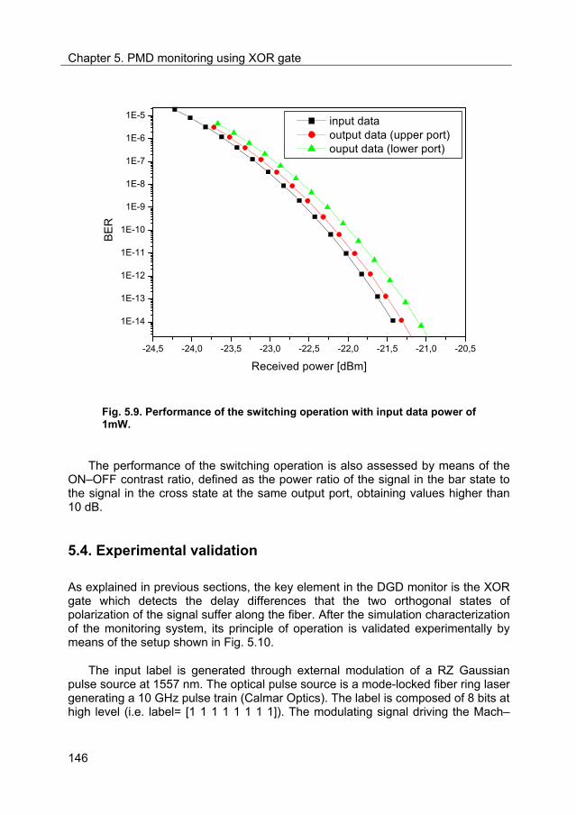
Chapter 5. PMD monitoring using XOR gate
146
-24,5 -24,0 -23,5 -23,0 -22,5 -22,0 -21,5 -21,0 -20,5
1E-14
1E-13
1E-12
1E-11
1E-10
1E-9
1E-8
1E-7
1E-6
1E-5B
ER
Received power [dBm]
input data output data (upper port) ouput data (lower port)
Fig. 5.9. Performance of the switching operation with input data power of 1mW.
The performance of the switching operation is also assessed by means of the ON–OFF contrast ratio, defined as the power ratio of the signal in the bar state to the signal in the cross state at the same output port, obtaining values higher than 10 dB.
5.4. Experimental validation
As explained in previous sections, the key element in the DGD monitor is the XOR gate which detects the delay differences that the two orthogonal states of polarization of the signal suffer along the fiber. After the simulation characterization of the monitoring system, its principle of operation is validated experimentally by means of the setup shown in Fig. 5.10.
The input label is generated through external modulation of a RZ Gaussian pulse source at 1557 nm. The optical pulse source is a mode-locked fiber ring laser generating a 10 GHz pulse train (Calmar Optics). The label is composed of 8 bits at high level (i.e. label= [1 1 1 1 1 1 1 1]). The modulating signal driving the Mach–
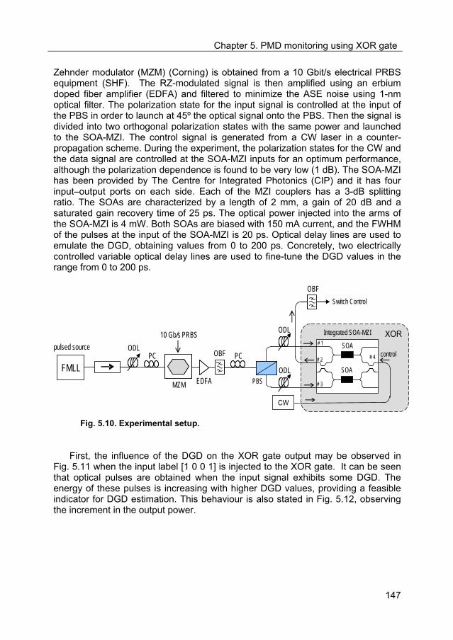
Chapter 5. PMD monitoring using XOR gate
147
Zehnder modulator (MZM) (Corning) is obtained from a 10 Gbit/s electrical PRBS equipment (SHF). The RZ-modulated signal is then amplified using an erbium doped fiber amplifier (EDFA) and filtered to minimize the ASE noise using 1-nm optical filter. The polarization state for the input signal is controlled at the input of the PBS in order to launch at 45º the optical signal onto the PBS. Then the signal is divided into two orthogonal polarization states with the same power and launched to the SOA-MZI. The control signal is generated from a CW laser in a counter-propagation scheme. During the experiment, the polarization states for the CW and the data signal are controlled at the SOA-MZI inputs for an optimum performance, although the polarization dependence is found to be very low (1 dB). The SOA-MZI has been provided by The Centre for Integrated Photonics (CIP) and it has four input–output ports on each side. Each of the MZI couplers has a 3-dB splitting ratio. The SOAs are characterized by a length of 2 mm, a gain of 20 dB and a saturated gain recovery time of 25 ps. The optical power injected into the arms of the SOA-MZI is 4 mW. Both SOAs are biased with 150 mA current, and the FWHM of the pulses at the input of the SOA-MZI is 20 ps. Optical delay lines are used to emulate the DGD, obtaining values from 0 to 200 ps. Concretely, two electrically controlled variable optical delay lines are used to fine-tune the DGD values in the range from 0 to 200 ps.
ODLPC
EDFA
OBF
10 Gb/s PRBS
MZM
PC control
PBS
SOA
SOA
Integrated SOA-MZI# 1
# 2
# 3
# 4
CW
Switch Control
XORODL
ODL
OBF
FMLL
pulsed source
Fig. 5.10. Experimental setup.
First, the influence of the DGD on the XOR gate output may be observed in Fig. 5.11 when the input label [1 0 0 1] is injected to the XOR gate. It can be seen that optical pulses are obtained when the input signal exhibits some DGD. The energy of these pulses is increasing with higher DGD values, providing a feasible indicator for DGD estimation. This behaviour is also stated in Fig. 5.12, observing the increment in the output power.

Chapter 5. PMD monitoring using XOR gate
148
DGD=0 ps DGD= 20 ps DGD= 50 ps
TE
TM
TETE
TMTM
Output XOR Output XOR Output XOR
DGD=0 ps DGD= 20 ps DGD= 50 psDGD=0 ps DGD= 20 ps DGD= 50 ps
TE
TM
TETE
TMTM
Output XOR Output XOR Output XOR
Fig. 5.11. Effect of the first-order PMD on the XOR gate output, label =[1 0 0 1] (Time: 100ps/div).
A)
B)
C)
D)
E)
F)
A)
B)
C)
D)
E)
F)
Time: 50 ps/div
A)
B)
C)
D)
E)
F)
A)
B)
C)
D)
E)
F)
A)
B)
C)
D)
E)
F)
A)
B)
C)
D)
E)
F)
A)
B)
C)
D)
E)
F)
Time: 50 ps/div
Fig. 5.12. XOR output for different DGD values (label = [1 0 0 1]): (A) 0 ps; (B) 25 ps; (C) 50 ps; (D) 100 ps; (E) 150 ps; (F) 200 ps.

Chapter 5. PMD monitoring using XOR gate
149
Now, the monitoring system is validated by introducing the input label [1 1 1 1 1 1 1 1] at 10 Gbit/s. Fig. 5.13 shows the average power of these pulses as a function of the DGD value. It can be seen that the average power is less than 10 dBm when the DGD value is nearly zero, as the two data signals at the input of the XOR gate are almost synchronized. When the DGD is higher, some pulses appear at the output of the XOR gate and the average power increases. The maximum average power is achieved for a DGD value equal to half the bit period (this maximum depends on the pulse width). From the maximum on, the data signals start being overlapped again and so the average power begins to decrease to a local minimum. This minimum is obtained for a DGD equal to the bit period. However, some average power is measured for DGD = 100 ps because the optical label has finite length (8 bit) and two optical pulses appear at the output of the XOR gate in this case. The solid line corresponds to the experimental measurements (FWHM ~ 20 ps), whereas the dashed-dotted lines are simulation results (FWHM = 10, 20 and 25 ps). A good correlation between both results can be observed. The slight deviation is produced by the ASE noise introduced by the EDFA and the SOA-MZI. Indeed, for low DGD values, where the output power is very low and the average power is dominated by the noise level, such slope deviation is produced because the noise generated by the VPI is not exactly the same as the real noise.
20 40 60 80 100 120
-11.5
-11
-10.5
-10
-9.5
-9
-8.5
-8
-7.5
-7
-6.5
DGD (ps)
Ave
rage
pow
er
(dB
m)
experiment
simulation(FWHM = 10 ps)
simulation(FWHM = 20 ps)
simulation(FWHM = 25 ps)
Fig. 5.13. Average power at the output of the XOR gate as a function of DGD value: simulations and experiment (Input label = [1 1 1 1 1 1 1 1]).

Chapter 5. PMD monitoring using XOR gate
150
To overcome this mismatch between the simulation and experimental curves for low DGD values, a training of the system should be done at the first stage of the transmission. During the training process, the DGD monitor calculates the output power of the system for different DGD values and adjusts the curve which will be used for DGD monitoring. Afterwards, from the measured output power the DGD will be estimated.
In conclusion, these experimental results validate the monitoring approach. The next step consists of using these output pulses from the XOR gate as the control signal for an optical switch. The use of a SOA-MZI as latching switch was already demonstrated in [Cla06]. To achieve proper operation, the input set and reset pulses must provide enough energy. This may be controlled by using an EDFA at the output of the XOR monitor to set the DGD threshold. So the proposed approach is a flexible and viable technique to address packet routing decisions based on performance monitoring in packet-switched networks.
5.5. Summary and conclusions
With the increasing interest in performing the basic networking functionalities in the optical domain to achieve bitrate transparency, all-optical logic gates have become key elements in the implementation of such functionalities. Apart from the importance of logic gates in the field of optical signal processing, in this Chapter an all-optical DGD monitor based on a logic XOR gate for OPS networks has been proposed. This XOR-based DGD monitor detects the delay differences that the two orthogonal states of polarization of the signal suffer along the fiber, obtaining an increment in the output pulse power as DGD increases. On the other hand, the output of the XOR gate acts as the control signal for an all-optical 1x2 packet switch operating in a similar way to an optical flip-flop. Therefore, the whole proposed system is based on all-optical logic gates, particularly a XOR gate and an optical flip-flop.
SOA-based architectures are very attractive to implement these logic gates since they can exhibit a strong change of the refractive index together with high gain. Furthermore, SOAs allow for photonic integration. Indeed, photonic integration seems to be a very promising solution to make this kind of architectures more compact and scalable. Among all the architectures, SOAs under a MZI configuration show very good results as well as being a very versatile scheme to implement the most important logic functions [Fje00, Kan00, Kim06]. Concretely, in this Chapter a logic XOR gate implemented in an integrated SOA-MZI for DGD monitoring has been proposed. In addition, the all-optical 1x2 packet switch is also based on a SOA-MZI with a feedback loop operating as an optical flip-flop.

Chapter 5. PMD monitoring using XOR gate
151
In this Chapter, the principle of operation of the proposed monitoring system has been described. First, the basis of the XOR-based DGD monitor implemented in a SOA-MZI has been presented. Later on, real-time packet routing decisions have been demonstrated by using the output of the DGD monitor as the control signal for the all-optical latching circuit. Once introduced their principle of operation, the architecture has been tested by means of simulations using the Virtual Photonics Inc. software. These simulations have successfully validated the operation of all the blocks of the system. In fact, simulation results have shown that the XOR gate output can be used as a feasible indicator of the DGD value and that the packets can be switched to a specific port depending on the estimated DGD value. Finally, experimental results have been carried out to demonstrate the XOR-based monitoring subsystem, showing similar behaviour to the simulations results.
Although the SOA-MZI architecture is very versatile and allows photonic integration, the use of SOAs with slow recovery times introduces a limitation in the operating bitrate of the gate. As commented at the beginning of the Chapter, the reason of using a label with bitrate lower than the packet was that the processing of such labels was mainly limited by this technological constraint, limiting the operation to 10 Gbit/s. However, the implementation of the differential scheme approach reduces this limitation, enabling the operation with 40 Gbit/s data signals [Web03]. Fig. 5.14 shows the proposed architecture of the XOR-based DGD monitor with the differential block placed at the input of the SOA-MZI.
OBF
CW
Integrated SOA-MZI
ControlSOA# 1
SOA# 2
# 3
# 4
Switch Control
PBS
TE
TMODL
ODL XOR
Differential scheme
Label @ 40 Gb/s
OBF
CW
Integrated SOA-MZI
ControlSOA# 1
SOA# 2
# 3
# 4SOA# 1
SOA# 2
# 3
# 4
SOA# 2
# 3
# 4
Switch Control
PBS
TE
TMODL
ODL XOR
Differential scheme
Label @ 40 Gb/s
Fig. 5.14. Proposed architecture of the XOR-based DGD monitor with the differential scheme

Chapter 5. PMD monitoring using XOR gate
152
After the PBS, the two orthogonal polarization states are combined by using the differential scheme as follows: in port #1, TE state data is combined with a delayed and attenuated version of the TM state data, while in port #3, TM state data is combined with a delayed and attenuated version of the TE state data. By properly adjusting the values of these delays and attenuations, the logic XOR operation of the 40-Gbit/s input data is performed. Moreover, together with the differential scheme, a pre-processing state comprised of an optical sampler and a time-stretcher may be used to reduce the speed requirements.
Up to now, the advantages of using optical gates for monitoring purposes have been commented. However, the main advantage of the proposed monitoring is its ability to monitor the DGD on a packet-by-packet basis. In fact, DGD is a critical limiting factor in OPS networks operating at high bitrates. Thus, DGD monitoring is essential for signal quality management in these networks. Therefore, a DGD monitor with fast response and “on-the-fly” operation is highly desirable. As it was just said, the proposed scheme allows real-time DGD monitoring at the optical domain, offering a promising solution due to its simplicity, scalability, and integration capability. Furthermore, this technique provides a better quality estimation of the PMD values than electronic-measurement-based techniques since the measurements are directly done at the optical domain.
Due to the statistical nature of PMD, it is not only important to find convenient way to perform the monitoring in real-time, but also to adapt dynamically optical or electronic equalisation/mitigation elements [Kho01, Der02, Lan04]. At this point, a PMD compensator block may be included in the proposed system so that PMD should also be compensated on a real-time, per-packet basis. Then, once determined the PMD value of the incoming packet, the polarization of both signal components can be altered to correct itself. Fig. 5.15 shows a conceptual diagram of the interaction between the DGD and PMD monitor.
Payload Label
Label
1x2 Switch
Switch Control
Payload
Drop port
Regenerationport
Label extraction
XOR-basedDGD Monitoring
DGD monitor
DGD Compensator
Payload Label
Label
1x2 Switch
Switch Control
Payload
Drop port
Regenerationport
Label extraction
XOR-basedDGD Monitoring
DGD monitor
DGD Compensator
Fig. 5.15. Conceptual diagram of the interaction between DGD monitor and the compensator element.

Chapter 5. PMD monitoring using XOR gate
153
On the other hand, another point of special interest is the possibility of taking real-time packet routing decisions according to the estimated DGD values. This feature allows the integration of the DGD monitor with switching nodes to provide certain level of network intelligence.

Chapter 5. PMD monitoring using XOR gate
154
5.6. References
[Bin02] C. Bintjas, N. Pleros, K. Yiannopoulos, G. Theophilopoulos, M. Kalyvas, H. Avramopoulos, G. Guekos, “All-optical packet address and payload separation”, IEEE Photon. Technol. Lett., vol. 14, no. 12, pp. 1728–1730, 2002.
[Blu00] D.J. Blumenthal, B.E. Olsson, G. Rossi, T.E. Dimmick, L. Rau, M. Masanovic, O. Lavrova, R. Doshi, O. Jerphagnon, J.E. Bowers, V. Kaman, L.A. Coldren, J. Barton, “All-optical label swapping networks and technologies”, IEEE/OSA J. Lightwave Technol., vol. 18, no. 12, pp. 2058-2075, 2000.
[Bos02] G. Bosco, B.E. Olsson, D.J. Blumenthal, “Pulsewidth distortion monitoring in a 40 Gbit/s optical system affected by PMD”, IEEE Photon. Technol. Lett., vol. 14, no. 3, pp. 307-309, 2002.
[Bul00] H. Bülow, W. Baumert, H. Schmuck, F. Mohr, T. Schulz, F. Kuppers, and W. Weiershausen, “Measurement of the maximum speed of PMD fluctuation in installed field fiber”, in Proc. of Optical Fiber Communication Conference (OFC’00), Baltimore (Maryland, USA), vol. 2, pp. 83–85, 2000.
[Che02] H. Chen, G. Zhu, Q. Wang, J. Jaques, J. Leuthold, A.B. Piccirrilli, and N.K. Dutta, “All-optical logic XOR using differential scheme and Mach-Zehnder interferometer”, Electron. Lett., vol. 38, no. 21, pp. 1271-1273, 2002.
[Cla05] R. Clavero, F. Ramos, and J. Marti, “All-optical flip-flop based on an active Mach-Zehnder interferometer with a feedback loop”, Opt. Letters., vol. 30, pp. 2861-2863, 2005.
[Cla06] R. Clavero, K. Schulze, J.M. Martinez, J. Herrera, F. Ramos, J. Marti, “All-optical self-routing packet switch based on active Mach-Zehnder interferometer latching circuit”, in Proc. of 32nd European Conference on Optical Communication (ECOC’06), Cannes (France), vol. 3, pp. 299-300, 2006.
[Der02] A. Deragon, and J. Ferry, “Measuring and compensating for PMD in high-speed optical networks,” White Paper from NetTest, 2002.
[Fje00] T. Fjelde, D. Wolfson, A. Kloch, B. Dagens, A. Coquelin, I. Guillemot, F. Gaborit, F. Poingt and M. Renaud, “Demonstration of 40 Gbit/s all-optical logic XOR in integrated SOA-based interferometric wavelength converter”, Electon. Lett., vol. 36, no. 22, pp. 1863-1864, 2000.
[Ito02] T. Ito, R. Sato, R. Kasahara, I. Ogawa, Y. Kawaguchi, Y. Shibata, A. Ohki, “80 Gbit/s PMD compensation using a hybrid integrated all-optical EXOR circuit”, in Proc. of 28th European Conference on Optical Communication (ECOC’02), Copenhagen (Denmark), vol. 3, pp. 1-2, 2002.

Chapter 5. PMD monitoring using XOR gate
155
[Kan00] B.K. Kang, J.H. Kim, Y.H. Park, S. Lee, Y.M. Jhon, D.H. Woo, S.H. Kim, and S.H. Park, “All-optical logic AND in a SOA-based Mach-Zehnder all-optical wavelength converter”, in Proc. of 13th Laser and Electro-Optics Society, Rio Grande (Puerto Rico), vol. 1, pp. 117-118, 2000.
[Kho01] R. Khosravani, S.A. Havstad, Y.W. Song, P. Ebrahimi, and A.E. Willner, “Polarization-mode dispersion compensation in WDM systems,” IEEE Photon. Technol. Lett., vol. 13, no. 12, pp. 1370–1371, 2001.
[Kim02] J.H. Kim, Y.M. Jhon, Y.T. Byun, S.Lee, D.H. Woo, and S.H. Kim, “All-optical XOR gate using a semiconductor optical amplifiers without additional beam,” IEEE Photon. Technol. Lett., vol. 14, no. 10, pp. 1436-1438, 2002.
[Kim06] J.Y. Kim, J.M. Kang, T.Y. Kim, and S.K. Han, “10 Gbit/s all-optical composite logic gates with XOR, NOR, OR and NAND functions using SOA-MZI structures,” Electron. Lett., vol. 42, no. 5, pp. 303-304, 2006.
[Lan02] S. Lanne, W. Idler, J.P. Thiery, J.P. Hamaide, “Fully automatic PMD compensation at 40 Gbit/s,” Electron. Lett, vol. 38, no. 1, pp. 40-41, 2002.
[Lan04] S. Lanne, and E. Corbel, “Practical considerations for optical polarization mode dispersion compensators,” IEEE/OSA J. Lightwave Technol., vol. 22, no. 4, pp. 1033-1040, 2004.
[Low87] A.J. Lowery, “A new dynamic semiconductor laser model based on the transmission line modelling method,” IEEE Proc. J. Optoelectron., vol. 134, pp. 281-289, 1987.
[Mar06] J.M. Martinez, J. Herrera, F. Ramos, and J. Marti, “All-optical address recognition scheme for label-swapping networks”, IEEE Photon. Technol. Lett., vol. 18, no. 1, pp. 151-153, 2006.
[Mas03] M.L. Masanovic, E.J. Skogen, J.S. Barton, V. Lal, D.J. Blumenthal, and L.A. Coldren, “Demonstration of monolithically-integrated InP widely-tunable laser and SOA-MZI wavelength converter,” in Proc. of Indium Phosphide and Related Materials, Santa Barbara (CA, USA), pp. 289-291, 2003.
[Noe99] R. Noe, D. Sandel, M. Yoshida-Dierolf, S. Hinz, V. Mirvoda, A. Schopflin, C. Gungener, E. Gottwald, C. Scheerer, G. Fischer, T. Weyrauch, and W. Haase, “Polarization mode dispersion compensation at 10, 20, and 40 Gbit/s with various optical equalizers”, IEEE/OSA J. Lightwave Technol., vol. 17, no. 9, pp. 1602-1616, 1999.
[Pat05] E.A. Patent, J.J.G.M. van der Tol, M.L. Nielsen, J.J.M. Binsma, Y.S. Oei, J. Mørk, and M.K. Smit, “Integrated SOA-MZI for pattern-effect-free amplification”, Electron. Lett., vol. 41, no. 9, pp. 549-551, 2005.
[Pou06] A. Poustie, “SOA based devices for all optical signal processing”, in Proc. of Optical Amplifiers and their Applications (OAA 2006), Atlanta (USA), paper

Chapter 5. PMD monitoring using XOR gate
156
OTuC1, 2006.
[Pua00] H.P. Pua, K. Peddanarappagari, B. Zhu, C. Allen, K. Demarest, and R. Hui,“An adaptive first-order polarization-mode dispersion compensation system aided by polarization scrambling: theory and demonstration,” IEEE/OSA J. Lightwave Technol., vol.18, no. 6, pp. 832-841, 2000.
[Sun02] H. Sunnerud, M. Karlsson, X. Chongjin, and P.A. Andrekson, “Polarization-mode dispersion in high-speed fiber-optic transmission systems,” IEEE/OSA J. Lightwave Technol., vol. 20, no. 12, pp. 2204-2219, 2002.
[Tak94] T. Takahashi, T. Amai, and M. Aiki, “Automatic compensation technique for timewise fluctuating polarisation mode dispersion in in-line amplifier systems,” Electron. Lett., vol. 30, no. 4, pp. 348-349, 1994.
[Web03] R.P. Webb, R.J. Manning, G.D. Maxwell, and A.J. Poustie, “40 Gbit/s all-optical XOR gate based on hybrid-integrated Mach-Zehnder interferometer,” Electron. Lett., vol. 39, no. 1, pp. 79-81, 2003.
[Wil04] A.E. Willner, S.M.M. Nezam, L. Yan, Z. Pan, and M.C. Hauer, “Monitoring and control of polarization-related impairments in optical fiber systems”, IEEE/OSA J. Lightwave Technol., vol. 22, no. 1, pp. 106-125, 2004.

157
Chapter 6
All-optical TTL decrementing using XOR gates
6.1. Introduction
In OPS networks, the optical label is used to make routing decisions and forwarding operations at the optical nodes. Apart from this functionality, the processing of the optical labels allows new optical signal processing technologies to be implemented to facilitate high-performance packet routing and networking, such as optical time-to-live (TTL) [Yoo05].
Routing loop is a serious problem in packet-switched networks, which can cause severe overload and congestion in the network [Pax97]. Unlike electronic IP networks, OPS networks can have long fiber links between optical router hops, and fiber transmission errors may create errant packets. One commonly-employed method to prevent these loops from strangling the bandwidth of a network is to use a “time-to-live” (TTL) field within the label of a packet. The TTL field determines the maximum numbers of hops a packet can take before getting dropped for being too “old” for the network.
Following this concept, the TTL technique can also be effective as an OPM technique. Every time a packet goes through one hop in the network its quality is reduced. So the maximum degradation that a packet can support matches a maximum number of router hops (TTL value).
Chapter 6. All-optical TTL monitoring using XOR gates
158
On the other hand, the TTL-based monitoring technique allows OPS networks to offer differentiated services to accommodate the different requirements of various clients [Ben00, Kil04]. Packets entering the network must be analyzed to determine their QoS requirements depending on the kind of network service, and then, the TTL value corresponding to the network service is determined. Then, the maximum number of router hops (TTL value) refers to the maximum degradation that a packet can support depending on the type of service transmitted.
Recent works have demonstrated optical TTL using ultra-short pulse bursts and nonlinear effects [Hun02, McGe03], but these methods are complex and difficult. Another TTL method is based on OSNR [Yang04] which requires electronic label processing. However, all-optical techniques are desirable in high-speed OPS networks because they provide low latency and can process the optical packets “on-the-fly”.
In this Chapter, a novel TTL method based on the use of optical logic XOR gates is proposed. All-optical decrementing of a packet’s TTL field requires optical implementation of a binary subtraction algorithm which is based on decrementing-via-inversion. The 1-bit subtractor is demonstrated employing a cascade of two SOA-based Mach-Zehnder interferometers (SOA-MZIs). In Section 2 the principle of operation is explained and the architecture of the subtractor is presented. In Section 3 the proposed technique is validated by means of simulations, showing a good extinction ratio (higher than 10 dB) at the output of the 1-bit subtractor. Conclusions are addressed in Section 4.
6.2. TTL-based monitoring system
6.2.1. Basis of the TTL-based monitoring
The packets in transparent OPS networks remain in the optical domain where the OSNR of the packets will decrease as the packets go through more hops in the network, due to repeated attenuation and amplifications at each router and fiber links. In order to illustrate this effect, the degradation experienced by the packets in each node is monitored by using the optical performance monitoring configuration shown in Fig. 6.1. An optical packet is transported through a series of optical routers to its destination. Optical taps at various network sites are used to monitor the optical signal in the network.

Chapter 6. All-optical TTL monitoring using XOR gates
159
Source . . . Destination
OPM OPM OPM
Source . . . Destination
OPM OPM OPM
Fig. 6.1. Optical performance monitoring network configuration. Monitors (OPM) are placed at taps in various network sites.
In a generic 30-nodes network, the OSNR monitoring behaviour is examined [Kil03]. The signal power is assumed to be constant at all nodes, and therefore noise is measured relative to the signal power as the inverse of the OSNR. Fig. 6.2 shows the OSNR as a function of distance or number of nodes. Considering different end terminal BER values (curves for 10-12 down to 10-5 BER), the maximum OSNR degradation that packets can suffer to fulfil certain quality level can be extracted. For example, the difference between the curve for 10-12 and the curve for 10-9 is the minimum OSNR degradation at each node (monitoring point) that will pull the end terminal BER below the threshold of 10-9. For the first ten nodes, the OSNR drops rapidly from one node to the next so one expects large drops in OSNR in order to impact the BER. Beyond ten nodes, the OSNR drops more gradually from node to nodes and smaller changes in OSNR can impact the end terminal BER. Then, in order to guarantee a certain signal quality at the end terminal, the number of hops inside the network must be limited.
BER
10- 12
10- 9
10- 5
Nodes #
OS
NR
(dB
)
BER
10- 12
10- 9
10- 5
Nodes #
OS
NR
(dB
)
Fig. 6.2. OSNR as a function of node number or distance [Kil03].
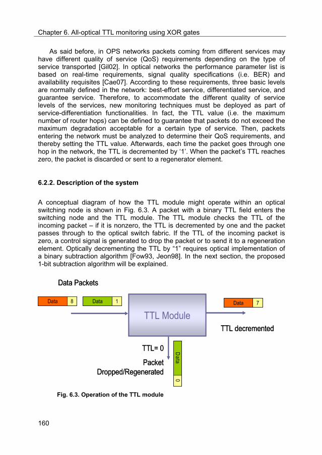
Chapter 6. All-optical TTL monitoring using XOR gates
160
As said before, in OPS networks packets coming from different services may have different quality of service (QoS) requirements depending on the type of service transported [Gil02]. In optical networks the performance parameter list is based on real-time requirements, signal quality specifications (i.e. BER) and availability requisites [Cae07]. According to these requirements, three basic levels are normally defined in the network: best-effort service, differentiated service, and guarantee service. Therefore, to accommodate the different quality of service levels of the services, new monitoring techniques must be deployed as part of service-differentiation functionalities. In fact, the TTL value (i.e. the maximum number of router hops) can be defined to guarantee that packets do not exceed the maximum degradation acceptable for a certain type of service. Then, packets entering the network must be analyzed to determine their QoS requirements, and thereby setting the TTL value. Afterwards, each time the packet goes through one hop in the network, the TTL is decremented by ‘1’. When the packet’s TTL reaches zero, the packet is discarded or sent to a regenerator element.
6.2.2. Description of the system
A conceptual diagram of how the TTL module might operate within an optical switching node is shown in Fig. 6.3. A packet with a binary TTL field enters the switching node and the TTL module. The TTL module checks the TTL of the incoming packet – if it is nonzero, the TTL is decremented by one and the packet passes through to the optical switch fabric. If the TTL of the incoming packet is zero, a control signal is generated to drop the packet or to send it to a regeneration element. Optically decrementing the TTL by “1” requires optical implementation of a binary subtraction algorithm [Fow93, Jeon98]. In the next section, the proposed 1-bit subtraction algorithm will be explained.
TTL Module
TTL= 0
PacketDropped/Regenerated
TTL decremented
Data Data
Data Packets
Data
Data
8 71
0
TTL Module
TTL= 0
PacketDropped/Regenerated
TTL decremented
Data Data
Data Packets
Data
Data
8 71
0
Fig. 6.3. Operation of the TTL module

Chapter 6. All-optical TTL monitoring using XOR gates
161
6.2.3. 1-bit binary subtraction
Decrementing a TTL field by “1” requires the implementation of a binary subtraction algorithm. Considering any arbitrary starting binary word this results in the least-significant-bit (LSB) being inverted (1 minus 1 is 0, while 0 minus 1 results in 1). If the LSB is a “1” bit, the subtraction is complete, as no borrowing is necessary. However, if the LSB is a “0” bit, the next higher column must be reduced by “1” as a result of the borrowing process. This process continues with additional borrowing until a “1” bit is encountered. After inverting the “1” bit, the subtraction is completed. Next the 1-bit subtraction process is shown with two examples in Fig. 6.4.
1 0 0 0 1 1LSBMSB
1
1 0 0 0 1 0
1 0 0 1 0 0LSBMSB
1
1 0 0 0 1 1
1 0 0 0 1 1LSBMSB
1
1 0 0 0 1 0
1 0 0 1 0 0LSBMSB
1
1 0 0 0 1 1
Fig. 6.4. Examples of the 1-bit subtraction process.
As it can be seen, this results in a set of bits being replaced by their conjugates (beginning with the LSB up-to-and-including the first “1” bit).
6.2.4. Architecture of the 1-bit binary subtractor
Decrementing the TTL field requires editing the packet header, something easy in electronics, but often difficult in optical systems. Indeed, previous approaches to implement an all-optical binary subtractor are complex. In this section, a novel TTL method based on the use of optical logic XOR gates implemented in SOA-MZI devices is proposed. The architecture of the 1-bit binary subtractor is shown in Fig. 6.5. It is mainly based on two SOA-MZI devices configured as a Boolean logic XOR gate [Mar02]. The first XOR gate is a SOA-MZI with feedback architecture. However, the second gate is based on the principle of operation of the XOR gate explained in the Chapter 5. Both SOA-MZIs are normally off (i.e. phase difference between the arms), so the control pulses only appear at the output if both data inputs are different. The proper interconnection between the two XOR gates leads to the desired subtraction operation explained above.

Chapter 6. All-optical TTL monitoring using XOR gates
162
outputOBF
Integrated SOA-MZI
DecrementedTTL field
OBF
Output XOR1
Integrated SOA-MZI
Feedback loop
Control
1- Initial pulse
saturableabsorber
Control1-bit timedelay
TTL field
ODL
SOA
# 1
# 2
# 3
SOA
SOA
# 4
# 1
# 2
# 3
Pulse trainXOR 1
SOA
SOA
# 4
XOR 2
outputOBF
Integrated SOA-MZI
DecrementedTTL field
OBF
Output XOR1
Integrated SOA-MZI
Feedback loop
Control
1- Initial pulse
saturableabsorber
Control1-bit timedelay
TTL field
ODL
SOA
# 1
# 2
# 3
SOA
SOA
# 4
SOA
SOA
# 4
# 1
# 2
# 3
Pulse trainXOR 1
SOA
SOA
# 4
SOA
SOA
# 4
XOR 2
Fig. 6.5. Architecture of the all-optical 1-bit TTL subtractor.
XOR with feedback structure
The all-optical XOR gate with feedback consists of a Mach-Zehnder Interferometer (MZI) structure, in which there is one SOA placed in each branch of the interferometer, followed by a feedback network, which will adapt the output of the gate to become the control signal for successive comparisons. The feedback loop consists of an optical amplifier, an optional band-pass filter and a delay element for time synchronization between pulses. The optical filter, centred at the control signal wavelength, reduces the propagation of ASE noise through the feedback loop. Moreover, the optical amplifier adjusts the power level of the output pulses so that a feedback loop gain close to the unity is achieved. To avoid lasing at the operating wavelength, a phase shifter may be used.
Fig. 6.6 shows how two data signals enter into the gate, coupled with the control signal. In this architecture a pulsed optical signal is used as the control signal. This control signal enables the device operation. Only when an optical pulse is present at the input #4 of the SOA-MZI, the 1-bit logic XOR operation is performed. The control signal must be matched temporally with the first bit of the sequences to compare. Data signals and the control signal counter-propagate

Chapter 6. All-optical TTL monitoring using XOR gates
163
inside the SOAs to avoid crosstalk. Furthermore, when the two incoming bits are different, the output of the SOA-MZI (port #2) is also an optical pulse, which after optically processed is feedback to the input of the SOA-MZI (port #4) as an enabling signal for the comparison of the next two bits. Otherwise (i.e. incoming compared bits are the same), no pulse at the output is obtained and the gate is disabled.
outputOBF
Integrated SOA-MZI
Control Signal
SOA
# 1
# 2
# 3
SOA
SOA
# 4
XOR 1
Data 1
Data 2
ODL
outputOBF
Integrated SOA-MZI
Control Signal
SOA
# 1
# 2
# 3
SOA
SOA
# 4
SOA
SOA
# 4
XOR 1
Data 1
Data 2
ODL
Fig. 6.6. XOR with feedback architecture.
Once introduced the principle of operation of the XOR with feedback structure, the architecture of the 1-bit binary subtractor is explained in detail.
The power of the incoming TTL word is split: one fraction enters the first XOR gate (XOR1) through port #1 after a 1-bit time delay, whereas the other enters the second one (XOR2) through port #1. The logic XOR1 gate has a feedback loop which redirects its output pulses as a control signal for the successive incoming bits, as commented before [Mar06]. These control pulses act as enabling signal for the XOR gate. As a result of the interconnection of Fig. 6.5, optical pulses are obtained at the output port #2 of XOR1 as long as the two data bits (input ports #1 and #3) are different and the control signal (port #4) is at high level. If there is a bit comparison between two data bits which are the same, then no output pulse is obtained at port #2 and the gate is inhibited, as the control signal will be at low level from now on. The output from XOR1 is then used as one of the two data inputs to XOR2. In this case, the control signal is a pulse train. At the output of XOR2, a 1-bit decremented TTL field is obtained. Finally, the signal is filtered again, as well as power equalized using a saturable absorber.

Chapter 6. All-optical TTL monitoring using XOR gates
164
An example of operation of the 1-bit subtractor is schematically depicted in Fig. 6.7 and Fig. 6.8, whereas its Boolean logic principle of operation is explained in Fig. 6.9. The gate requires control pulses to do the XOR operation. Otherwise it is disabled and no output is obtained. So the control input is also used to disable the gate when required (after the first “1” bit in the TTL input). The initial pulse is needed to enable the XOR gate initially and must be synchronized with the TTL signal. Synchronization issues can be addressed in a similar way to that shown in [Keh06].
1
XOR
TTL
1 – Initial pulse
1‐bit time delay
Feedback loop
MSB0 1 0 0
0 1 1 1 1
0 1 0 0 0
0 1 0 0
1 1 1 1 1
LSB
A)B)
C)
XORControl
TTL
Data B
0 0 1 1 1
0 0 1 1
D)
E)
0 1 0 0
1
MSB LSB
0 0 1 1
1
XOR
TTL
1 – Initial pulse
1‐bit time delay
Feedback loop
MSB0 1 0 0
0 1 1 1 1
0 1 0 0 0
0 1 0 0
1 1 1 1 1
LSB
A)B)
C)
XORControl
TTL
Data B
0 0 1 1 1
0 0 1 1
D)
E)
1
XOR
TTL
1 – Initial pulse
1‐bit time delay
Feedback loop
MSB0 1 0 0
0 1 1 1 1
0 1 0 0 0
0 1 0 0
1 1 1 1 1
LSB
A)B)
C)
1
XOR
TTL
1 – Initial pulse
1‐bit time delay
Feedback loop
MSB0 1 0 0
0 1 1 1 1
0 1 0 0 0
0 1 0 0
1 1 1 1 1
LSB
A)B)
C)
XOR
TTL
1 – Initial pulse
1‐bit time delay
Feedback loop
MSB0 1 0 0
0 1 1 1 1
0 1 0 0 0
0 1 0 0
1 1 1 1 1
LSB
A)B)
C)
XORControl
TTL
Data B
0 0 1 1 1
0 0 1 1
D)
E)XOR
Control
TTL
Data B
0 0 1 1 1
0 0 1 1
D)
E)
0 1 0 0
1
MSB LSB
0 0 1 1
0 1 0 0
1
MSB LSB
0 0 1 1
Fig. 6.7. Example of operation. TTL= [0 1 0 0]; 1-bit decremented TTL= [0 0 1 1].

Chapter 6. All-optical TTL monitoring using XOR gates
165
B)
A) 1 000
MSBLSB
E)
D)
C)
1 1 00
Initialpulse
B)
A) 1 000
MSBLSB
E)
D)
C)
1 1 00
Initialpulse
Fig. 6.8. Detail of the signals in several points of the architecture, showing the operation of the whole system for TTL= [0 1 0 0].
As explained in the 1-bit binary subtraction algorithm, to achieve a binary subtraction, a set of bits are replaced by their conjugates (beginning with the LSB up-to-and including the first ‘1’ bit). Therefore, the first XOR gate provides ‘1’ bits up to the first ‘1’ bit in the TTL input. So the second XOR gate conjugates the TTL input bits up-to-and including the first ‘1’ bit, leading to the desired subtraction operation (see Fig. 6.9).

Chapter 6. All-optical TTL monitoring using XOR gates
166
0 1 1 1
0 1 0 0
0 0 1 1
0 1 0 0 0
0 1 1 1 1
0 0 1 1 1
1 bit delay
TTL input:
Output XOR1:
initial pulsegate disabledfrom now on(control input)
TTL input:
Output XOR2:
XOR1
XOR2
gate alwaysenabled
Output XOR1:
Fig. 6.9. Principle of operation of the 1-bit subtractor: Boolean logic.
6.3. Results and discussion
The proposed TTL decrementing technique is tested by means of simulations using the Virtual Photonics Inc. software VPI.7.1. These simulations aim to demonstrate the subtraction operation employing practical devices. The VPI simulation schematic for all-optical TTL decrementing follows the configuration illustrated in Fig. 6.5. This scheme is mainly based on two SOA-MZI devices configured as a Boolean logic XOR gate. The first XOR gate is a SOA-MZI with feedback architecture. However, the second gate is based on the principle of operation of the XOR gate explained in the Chapter 5. The physical parameters of the SOAs of the MZI are optimized to perform the XOR operation (The SOAs of both XOR gates have the same physical parameters), shown in Table 6.1.
The input TTL signal at 1558 nm is generated by externally modulating at 10 Gb/s an RZ Gaussian pulse source (FWHM = 5 ps). The data peak power at the input of the SOA-MZIs is adjusted to 3 mW. In the case of the XOR gate with the feedback loop, an initial pulse is needed to enable the XOR gate initially. To this end, an RZ Gaussian pulse source at 1558 nm is used. After that, the feedback loop redirects the XOR output as a control signal for the successive incoming bits. The feedback loop consists of an optical amplifier, an optical filter and a delay element. The gain amplifier is properly adjusted to have a loop gain close to the unity. The optical delay is also tuned to synchronize the control signal with the input TTL signal. In the case of the second XOR gate, the control signal is a pulse train

Chapter 6. All-optical TTL monitoring using XOR gates
167
at 1558 nm with a pulse peak power of 2 mW and a FWHM of 5 ps. In both XOR gates, a pump signal at 1550 nm is applied to the SOA-MZIs to accelerate the SOAs carrier density response. The power of the pump signal is 10 mW. Reference is made to Appendix B (Section 2) for further details of the VPI simulation setup.
Table 6.1. SOA physical parameters used in simulations of both XOR gates.
Parameter Value
SOA bias current 250 mA
SOA length 600 m
SOA linewidth enhancement factor 7
Spontaneous emission factor 0
Confinement factor 0.3
Initial carrier density 3.5x1024 1/m3
Carrier density transparency 1.5x1024 1/m3
The simulation results are shown in Fig. 6.10. The incoming TTL field (1101000) is depicted in Fig. 6.10.(a), whereas the output of the subtractor (1100111) is depicted in Fig. 6.10.(b). The LSB enters first in time into the subtractor. As it can be seen, the architecture works properly (a set of bits being replaced by their conjugates, beginning with the LSB up-to-and-including the first “1” bit: 1101000 – 1 = 1100111). In order to equalize the power levels of the output signal, a saturable absorber was used in the results of Fig. 6.10.(c). The performance of the technique is assessed by means of the extinction ratio, obtaining values higher than 10 dB. Although RZ signals are used, the proposed system also works for a NRZ TTL input provided that RZ control pulses are injected into the XOR gates.
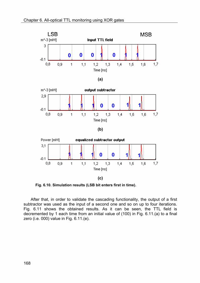
Chapter 6. All-optical TTL monitoring using XOR gates
168
MSBLSB
111 00 0 0
MSBLSB
111 00 0 0
(a)
11111 0 0 11111 0 0
(b)
1 1 1 1 1001 1 1 1 100
(c)
Fig. 6.10. Simulation results (LSB bit enters first in time).
After that, in order to validate the cascading functionality, the output of a first subtractor was used as the input of a second one and so on up to four iterations. Fig. 6.11 shows the obtained results. As it can be seen, the TTL field is decremented by 1 each time from an initial value of (100) in Fig. 6.11.(a) to a final zero (i.e. 000) value in Fig. 6.11.(e).

Chapter 6. All-optical TTL monitoring using XOR gates
169
100
MSBLSB
100
MSBLSB
(a)
11 011 0
(b)
10 010 0
(c)
1 0 01 0 0
(d)
0 0 00 0 0
(e)
Fig. 6.11. Example of recursive TTL decrementing reaching zero.

Chapter 6. All-optical TTL monitoring using XOR gates
170
The TTL decremented field emerged with a time delay of 29 ps in our simulations. This delay does not depend on the number of bits, but on the XOR gate processing time. Basically, the TTL processing time slightly increases the latency of the optical node.
As the TTL field is used to estimate the possible signal quality degradation (OPM technique) in terms of router hops, when this field reaches zero a control signal could be generated so that the router drops the packet or sends it to a regeneration element. To this end, an optical flip-flop circuit may be used [Cla04].
Finally, in order to test the performance of the proposed technique, the Q-factor is measured at the output of the subtractor for several recursive operations. The performance of the proposed architecture is dependent on the number of stages. The simulation results are depicted in Fig. 6.12, where the Q-factor of the output of the subtractor is depicted as a function of the iterations.
1 2 3 4 5 6 7 8 9 108
8.5
9
9.5
10
10.5
11
11.5
12
12.5
13
number of subtraction operations
Q fac
tor
(dB
)
Number of subtraction operations
Q-
fact
or (
dB)
1 2 3 4 5 6 7 8 9 108
8.5
9
9.5
10
10.5
11
11.5
12
12.5
13
number of subtraction operations
Q fac
tor
(dB
)
Number of subtraction operations
Q-
fact
or (
dB)
Fig. 6.12. Q factor of the TTL field as a function of the number of subtraction operations.

Chapter 6. All-optical TTL monitoring using XOR gates
171
As it can be seen in Fig. 6.12, the Q-factor is reduced when increasing the number of iterations due to the accumulated ASE noise introduced by the SOAs. Therefore, the 1-bit subtractor may be limited for a high number of operations. Obviously, the maximum number of subtractions (TTL field initial value) depends on specific parameters of the SOA-MZI devices and the ASE noise generated. Experimental demonstrations [Yux01] showed that up to 11 cascaded SOA may be used with good performance.
These simulation results are provided as a proof of concept and should be confirmed during the experimental phase. As said in Chapter 5, SOA-based architectures are very attractive to implement XOR logic gates as well as allowing photonic integration. In fact, architectures based on cascaded SOA-MZIs provide potentially to build a fully-integrated circuit. To this end, a photonic-integrated feedback loop is required in the first XOR gate [Mar06]. Short loops have long been a major deterrent for feedback based optical logic. The maximum overall loop delay allowed by the gate is given by 1/R, where R is the bitrate (100 ps @ 10 Gbit/s, or 25 ps @ 40 Gbit/s). To obtain a 100-ps round-trip time in the feedback loop (10 Gbit/s operation), small radius waveguide bends are needed which can be achieved employing high-index silica waveguides (~1-mm radius) or other fabrication technologies such as a deep/shallow double etching process (~100-μm radius) [Hill05]. For 40 Gbit/s operation and beyond, the use of new promising technologies such as two-dimensional photonic crystal (2D-PC) slabs for manufacturing ultra-small PICs are a suitable choice to implement the proposed architecture solving the speed constraint of the feedback loop [Tan02].
6.4. Conclusions
In typical IP networks packets incorporate a “time-to-live” (TTL) field to reduce the network congestion caused by misrouted packets. To this end, the TTL field is decremented by one at each hop within the network and when this value reaches zero, the packet is dropped. Following this concept, the proposed TTL technique is also a valuable technique for optical performance monitoring in packet-switched networks. Every time a packet goes through one hop in the network its quality is reduced. So the maximum degradation that a packet can support matches a maximum number of router hops (TTL value). Moreover, this field can be used to provide service-differentiation functionalities. Then, packets entering the network must be analyzed to determine their QoS requirements, and thereby setting the corresponding TTL value.
To begin a move toward all-optical routing within the network core, it may be necessary to implement this TTL decrementing process in the optical domain. In this Chapter, a novel TTL method based on the use of optical logic XOR gates has been proposed. The 1-bit subtractor is based on two cascaded SOA-MZIs in XOR configuration. The first XOR incorporates a feedback loop structure, as explained in

Chapter 6. All-optical TTL monitoring using XOR gates
172
Section 2. The proper interconnection between the two XOR gates leads to the desired subtraction operation.
To perform the all-optical TTL decrementing, a binary subtraction algorithm based on decrementing-via-inversion has been proposed. The implementation of this algorithm results in a set of bits being replaced by their conjugates, beginning with the LSB up-to-and-including the first “1” bit.
Simulation results have shown that SOA-MZI devices acting as logic XOR gates can be used as the main functional blocks to implement an all-optical TTL subtractor. If the value of the TTL field within the packet is nonzero, the TTL is decremented via a decrementing-via-inversion process and the packet passes through the module. If the TTL field reaches zero, however, the module generates a signal that can be used to drop the packet or send it to a regeneration element. This technique is independent of the length of the TTL and packet, demands no electronic control, and requires no guard time between the end of the TTL field and the rest of the packet.
The technique has been validated at 10 Gbit/s, although it may be also extended to higher bitrates. To this end, a photonic-integrated feedback loop is required in the first XOR gate. Moreover, another way to extend the bitrate operation of the TTL subtractor is by using a differential scheme placed at the input of the SOA-MZI. This solution enables the operation with 40 Gbit/s data signals as shown in [Web03].
The performance of the architecture has been assessed by using the extinction ratio, obtaining values higher than 10 dB. Furthermore, in order to validate the cascading functionality, the Q-factor has been measured at the output of the subtractor for several recursive operations, showing that the performance of the architecture is dependent on the number of iterations. The simulation results show that the Q-factor is reduced by increasing the number of bits, mainly due to ASE noise introduced by the SOAs. Obviously, the maximum number of subtractions (TTL field initial value) depends on specific parameters of the SOA-MZI devices and the ASE noise generated.

Chapter 6. All-optical TTL monitoring using XOR gates
173
6.5. References
[Ben00] G. Bendilli, C. Cavazzoni, R. Girardi, and R. Lano, “Optical performance monitoring techniques,” in Proc. of 26th European Conference on Optical Communication (ECOC’00), Munich (Germany), vol. 4, pp. 113-116, 2000.
[Cae07] R. van Caenegem, D. Colle, M. Pickavet, P. Demeester, K. Christodoulopoulos, K. Vlachos, E. Varvarigos, L. Stampoulidis, D. Roccato, and R. Vilar, “The design of an all-optical packet-switched network,” IEEE Commun. Mag., vol. 45, no. 11, pp. 52-61, 2007.
[Cla04] R. Clavero, J.M. Martinez, F. Ramos, and J. Marti, “All-optical packet routing scheme for optical label-swapping networks,” Opt. Express, vol. 12, no. 18, pp. 4326-4332, 2004.
[Fow93] R.E. Fowkes, “Hardware efficient algorithms for trigonometric functions,” IEEE Trans. Computers, vol. 42, pp. 235–239, 1993.
[Gil02] R. Giles, “Monitoring the optical networks,” in Proc. of Symposium on optical fiber measurements, Boulders (USA), pp. 19-24, 2002.
[Hill05] M.T. Hill, T. de Vries, H.J.S. Dorren, X.J.M. Leijtens, J.H.C. van Zantvoort, J.H. den Besten, E. Smalbrugge, Y.S. Oei, J.J.M. Binsma, G.D. Khoe, and M.K. Smit, “Integrated two-state AWG-based multiwavelength laser,” IEEE Photon. Technol. Lett., vol. 17, no. 5, pp. 956-958, 2005.
[Hun02] W. Hung, K. Chan, L.K. Chen, C.K. Chan, and F. Tong, “A routing loop control scheme in optical layer for optical packet networks”, in Proc. of Optical Fiber communication Conference (OFC’02), Anaheim (CA, USA), paper ThGG111, 2002.
[Jeon98] H.I. Jeon and M.A.G. Abushagur, “Digital optical arithmetic processor based on symbolic substitution,” in Proc. of 20th Southeastern Symp. Syst.Theory 1998, pp. 221–223, 1998.
[Keh06] E. Kehayas, J. Seoane, Y. Liu, J.M. Martinez, J. Herrera, P.V. Holm-Nielsen, S. Zhang, R. McDougall, G. Maxwell, F. Ramos, J. Marti, H.J.S. Dorren, P. Jeppesen, and H. Avramopoulos, “All-optical network subsystems using integrated SOA-based optical gates and flip-flops for label-swapped networks,” IEEE Photon. Technol. Lett., vol. 18, no. 16, pp. 1750-1752, 2006.
[Kil03] D.C. Kilper, and W. Weingartner, “Monitoring optical network performance degradation due to amplifier noise,” IEEE/OSA J. Lightwave. Technol., vol. 21, no. 5, pp. 1171–1178, 2003.
[Kil04] D.C. Kilper, R. Bach, D.J. Blumenthal, D. Einstein, T. Landolsi, L. Ostar,M. Preiss, and A.E.Willner, “Optical performance monitoring,” IEEE/OSA J.

Chapter 6. All-optical TTL monitoring using XOR gates
174
Lightwave Technol., vol. 22, no. 1, pp. 294–304, 2004.
[Mar02] J.M. Martinez, F. Ramos, J. Martí, J. Herrera, and R. Llorente, “All-optical N-bit XOR gate with feedback for optical packet header processing,” in Proc. of 28th European Conference on Optical Communication (ECOC’02), Copenhagen (Denmark), paper P4-8, 2002.
[Mar06] J.M. Martinez, J. Herrera, F. Ramos, and J. Martí, “All-optical correlation employing single logic XOR gate with feedback,” Electron. Lett., vol. 42, no. 20, pp. 1170-1171, 2006.
[McGe03] J. McGeehan, S. Kumar, D. Gurkan, S.M.R.M. Nezam, A.E. Willner, Parameswaran, M. M. Fejer, J. Bannister, and J.D. Touch, “All-optical decrementing of a packet’s time-to-live (TTL) field and subsequent dropping of a zero-TTL packet,” IEEE/OSA J. Lightwave Technol., vol. 21, no. 11, pp. 2746-2751, 2003.
[Pax97] V. Paxson, “End-to-End routing behavior in the internet,” IEEE/ACM Trans. Networking, vol. 5, no. 10, pp. 601-615, 1997.
[Tan02] Y. Tanaka, Y. Sugimoto, N. Ikeda, H. Nakamura, K. Asakawa, K. Inoue, “ Fabrication and characterization of symmetric Mach-Zehnder structure based on 2D photonic crystal waveguide for all-optical switches,” in Proc. of Lasers and Electro-Optics (CLEO’04), San Francisco (CA, USA), vol. 1, pp. 2, 2004.
[Web03] R.P. Webb, R.J. Manning, G.D. Maxwell, and A.J. Poustie, “40 Gbit/s all-optical XOR gate based on hybrid-integrated Mach-Zehnder interferometer,” Electron. Lett., vol. 39, no. 1, pp. 79-81, 2003.
[Yang04] J. Yang, Z. Zhu, H. Yang, Z. Pan, and S.J.B. Yoo, “All-optical time-to-live using error-checking labels in optical label switching networks,” in Proc. of 30th European Conference on Optical Communication (ECOC’04), Stockholm (Sweden), paper Th3.4.5, 2004.
[Yoo05] S. J. Ben Yoo, Z. Pan, H. Yang, and Z. Zhu, “All-optical signal processing in photonic label switching routers,” in Proc. of Optical Amplifiers and Their Applications Conference (OAAC), Budapest (Hungary), paper SuB1, 2005.
[Yux01] J. Yu, and P. Jeppesen, “Improvements of cascaded semiconductor optical amplifier gates by using holding light injection,” IEEE/OSA J. Lightwave. Technol., vol. 19, no. 5, pp. 614-623, 2001.

175
Chapter 7
PMD monitoring using RF tones
7.1. Introduction
In the Chapter 5 the importance of monitoring the Polarization Mode Dispersion (PMD) has been stated, especially when considering high-speed networks. In fact, PMD is considered one of the most important sources of transmission degradation, strongly limiting the performance of such next generation networks [Sun02]. PMD is different from other impairments due to its time-dependent variation which requires the monitoring of signal quality in an optical system in order to either dynamically tune a compensator or for network control and management. Thus, for the efficient compensation of PMD, the monitoring techniques should be able to accurately estimate the PMD value.
Unlike conventional optical communication, optical channels in OPS networks may consist of different packets. They could originate from diverse sources and traverse different optical links. In such a dynamic scenario, PMD must be monitored on a packet-by-packet basis and in real time.
As explained in Chapter 3, many monitoring techniques use spectral-tone-based RF spectrum measurements for signal quality monitoring. These techniques are very attractive due to their potential fast response time (sub-ms), its simplicity, and the fact that these spectral tones travel the complete optical path with the baseband signal so that are subject to the same degradations as the baseband signal.

Chapter 7. PMD monitoring using RF tones
176
Among the parameters that these techniques can monitor, it has been reported the PMD monitoring with high-frequency tones [Ros00, Nez01, Ji04] and also with the clock tones [Nez04a, Nez04b, Liz06]. The former techniques have some limitations, including: a) the spectral tone could interfere with the spectral components of data and cause power penalty, b) there are difficulties in making the effect of chromatic dispersion (CD) and PMD independent, c) the system performances could be deteriorated by the cross-gain modulation (XGM) of an erbium-doped fiber amplifier (EDFA) and/or stimulated Raman scattering (SRS) due to the ghost tone creation, and d) using high-frequency tones demand high bandwidth electronic devices [Sun97, Chu00]. The last techniques, based on clock tones, solve some of these limitations since they do not introduce any extra tone, but for high bitrates they still require high-frequency devices, increasing the cost of the system. To avoid the use of these high-frequency devices, in the Chapter 5 an all-optical PMD monitoring technique has been investigated. However, given the simplicity of the concept of RF spectrum measurements, in this Chapter, two clock-tone-based PMD monitoring techniques, which are CD and OSNR-insensitive, are proposed. The main feature of these techniques is that they provide a cost-effective solution appropriate for the high-speed networks.
Both PMD monitoring techniques are based on adding an additional optical carrier shifted with respect to the data carrier to create at very low frequencies new RF tones generated by the beating between the clock tone and this additional optical carrier. Unlike the other monitoring techniques presented in this Thesis, the first-order PMD monitoring methods proposed in this Chapter perform the monitoring by measuring the RF tone power. In previous chapters it has been explained that a specific field (i.e. monitoring field) is inserted into the optical label for monitoring purpose. However, the use of this concept in the RF spectrum measurement has an undesirable impact. If the monitoring-field length is too short, for example few bits, the sensitivity of the RF spectrum measurement is not quite accurate. Conversely, with just a slight increment in the length, e.g. 1% of the length of the packet, the monitoring field means an overhead that makes the efficiency of the transmission worse. There is then a trade-off between the sensitivity of the measurement and the efficiency of the transmission. To overcome these problems, the proposed techniques extract the PMD value from the measurement done over the whole packet. Thereby the overhead is avoided and the sensitivity of the technique is improved.
In this Chapter, Section 2 addresses a simulation study about the applicability of the monitoring techniques based on RF spectrum in OPS networks in terms of synchronization issues, time response, and sensitivity. Section 3 describes the principle of operation and the simulation results of the first PMD monitoring technique based on adding an additional optical carrier shifted with respect to the data optical carrier. In Section 4 another PMD monitoring method is explained. It is also based on adding a new optical carrier, but this time at the orthogonal polarization state. The proposed architecture is tested by means of simulations, and experimentally validated confirming the successful monitoring operation.

Chapter 7. PMD monitoring using RF tones
177
Finally, Section 5 gives the main conclusions derived from the work presented in this Chapter.
7.2. Study of the applicability of the monitoring techniques based on RF spectrum measurement in optical packet-switched networks
OPS networks are characterized by dynamic traffic scenarios where packets follow their own route along the network, being necessary the monitoring on a packet basis. Additionally, these networks require monitors with fast response and wide dynamic range. In this section, a study about the applicability of the monitoring techniques based on RF spectrum measurements is carried out. The analysis considers that the monitoring is performed on a packet basis which adds new challenges in terms of synchronization issues, time response of the monitor, and measurement sensitivity.
7.2.1. Synchronization issues
The monitoring system must exactly know when the packet arrives at the node in order to perform the monitoring tasks on the short time of one packet. In other words, the RF measurements must be done packet-by-packet.
In practice, synchronization function in the optical packet switching node can play a major role to control when a packet is present. The monitor should then cooperate with the synchronization function and the packet header processing unit should recover the clock on the packet, and in turn provides the timing information to the monitor to locate the packet. From now on, let us suppose that packet switching nodes have the capability of detecting the position of the packet for synchronization issues. As an example, in Chapter 3 it has been presented how the packet node can recover the packet clock and extract the monitoring-field [Bin02].
7.2.2. Response time
In OPS networks it is necessary to obtain fast response time for monitoring the optical packets. The monitoring techniques based on RF spectrum normally measure the RF tone power to extract the signal quality.
An RF power detector can directly measure the RF power in a frequency range. By using a fast RF power detector, a response time in the range of few

Chapter 7. PMD monitoring using RF tones
178
nanoseconds can be obtained. For example, commercial power detectors, such as a crystal detector, offer a time response of about 10 ns [Yi06].
7.2.3. Sensitivity analysis
Apart from requiring fast response time, monitoring techniques applicable to OPS networks should provide wide dynamic range which means exhibiting high sensitivity even with short packets. To analyze the sensitivity of the RF-spectrum-based techniques, a simulation study is carried out. The objective is to determine what the minimum packet length required by obtaining accurate measurement is. To this end, the simulation study is based on sending an RF tone attached into the packet. By varying the packet length, the impact of this parameter on the RF tone power is measured. In particular, Fig. 7.1 shows the dynamic range, which is measured as the extinction ratio of the RF tone, as a function of the packet length.
Packet Length (Bytes)
Ext
inct
ion
Rat
io (
dB)
Packet Length (Bytes)
Ext
inct
ion
Rat
io (
dB)
Fig. 7.1. Dynamic range measured as the extinction ratio of the RF tone vs packet length.
From Fig. 7.1 it can be seen that the dynamic range and, therefore, the measurement sensitivity increase when increasing the packet length. From a packet length higher than 1 Kbyte, the dynamic range stabilizes, obtaining good sensitivity for packets longer than 500 bytes. Note that the usual IP packet length varies between 500 bytes and 1500 bytes.

Chapter 7. PMD monitoring using RF tones
179
The next step is to study the sensitivity of the RF-tone-based monitoring technique versus the packet length taking into account different fiber degradations, such as CD and PMD. The effect of both CD and PMD on the RF tone power is the reduction of its power as these degradations are more present in the transmission link. Fig. 7.2 shows that for each CD value the higher the packet length is, the higher the sensitivity, and in turn the dynamic range. As a result, the monitoring errors decrease when increasing the packet length. Similar to the previous case, the dynamic range stabilizes when the packet length is longer than 500 bytes.
Ext
inct
ion
Ra
tio (
dB
)
0 200 400 600 800 10005
10
15
20
25
30
35
Packet Length (bytes)
CD=0ps/nm
CD=160ps/nm
CD=600ps/nm
CD=900ps/nm
Ext
inct
ion
Ra
tio (
dB
)
0 200 400 600 800 10005
10
15
20
25
30
35
Packet Length (bytes)
CD=0ps/nm
CD=160ps/nm
CD=600ps/nm
CD=900ps/nm
Fig. 7.2. Variation of the extinction ratio of the RF tone as a function of the packet length for different CD values.
As far as PMD is concerned, Fig. 7.3 shows the same behaviour as in the case of considering CD and thus the same conclusions can be drawn.

Chapter 7. PMD monitoring using RF tones
180
Ext
inct
ion
Rat
io (
dB)
Packet Length (Bytes)
0 200 400 600 800 10000
5
10
15
20
25
30
PMD=0ps
PMD=10psPMD=25ps
PMD=50ps
Ext
inct
ion
Rat
io (
dB)
Packet Length (Bytes)
0 200 400 600 800 10000
5
10
15
20
25
30
PMD=0ps
PMD=10psPMD=25ps
PMD=50ps
Fig. 7.3. Variation of the extinction ratio of the RF tone as a function of the packet length for different PMD values.
After the simulation study, it seems that the RF-spectrum-based monitoring techniques can be applied to the OPS networks since they provide fast response time and good sensitivity for the usual packet lengths travelling along the network.
In following sections, the principle of operation of the proposed first-order PMD monitoring techniques will be explained in more detail, and the simulation results and the experimental validation will be presented.
7.3. DGD monitoring using an additional shifted optical carrier
Given the stochastic nature of PMD, it is desirable to monitor PMD in order to dynamically tune a compensator and also to isolate the PMD effects from other physical impairments such as CD. As said previously, several PMD monitoring techniques based on pilot tones and clock tone power detection have been reported in the literature. Nevertheless, these techniques suffer from the requirement of high-speed electronics per-channel, while being bitrate or format-dependent - making them unsuitable for the future applications. In this section, a clock tone-based PMD monitoring technique which is CD and OSNR-insensitive is presented. Moreover, it provides a cost-effective solution appropriate for the high-speed networks.

Chapter 7. PMD monitoring using RF tones
181
7.3.1. Description of the DGD monitoring technique
The proposed first-order PMD monitoring technique is based on adding an additional optical carrier shifted with respect to the data carrier. Therefore, after detection, the added carrier beats with the upper and lower clock tones of the data generating beat signals at frequencies Rb ± fshift (Rb is the bitrate and fshift is the shift between the data carrier and the additional carrier). The resulting RF power of these beat signals depends on the PMD value. PMD causes orthogonal polarization modes to propagate at different velocities so that the upper and lower sidebands of the signal experience a phase difference that decreases the received RF clock tone power. This behaviour is described by the following equation [Ishi98]:
DGDfP RFRF 2sin)1(41 , (7.1)
where is the power ratio between the fast and slow axes, and fRF is the
frequency of the RF tone.
Hence, without DGD, the phase delay is equal to zero; so that the clock tones and the optical carrier remain in phase resulting in a maximum RF power. Conversely, as the DGD increases, the power of the beat RF tones decreases. In addition, it should be noted that a very low-frequency beat tone can be selected after detection by properly selecting fshift. Therefore, the power of the Rb fshift tone can be used for DGD monitoring of high-speed data with a low-speed detector providing a cost-effective solution. A conceptual diagram of the proposed technique is illustrated in Fig. 7.4.
Clock Tone
New beats: Rb ± fshift
Rb
Added carrier
fshift
Rb Freq (GHz)
RF P
ower Clock Tone
New beats: Rb ± fshift
Rb
Added carrier
fshift
Rb
Clock Tone
New beats: Rb ± fshift
Rb
Added carrier
fshift
Rb Freq (GHz)
RF P
ower
Fig. 7.4. Conceptual diagram of the PMD monitoring technique.

Chapter 7. PMD monitoring using RF tones
182
On the other hand, since the upper and lower optical clock tones are asymmetric with respect to the added shifted carrier, CD can only affect the phases of these new RF tones but not the amplitude. As a consequence, accurate CD-insensitive DGD monitoring is performed.
As commented in Chapter 3, due to the periodic nature of (7.1), DGD monitoring techniques based on clock tones have a limited monitoring range given by
bR
DGD2
1max , (7.2)
where Rb is the frequency of the clock tone.
From (7.2) it can be seen that the monitoring range is inversely proportional to the frequency used for monitoring. Thus, using the Rb fshift tone provides a high monitoring range, however, the sensitivity of the measurement is then reduced drastically.
For high bitrate data monitoring the RF power changes should be very sensitive to a small DGD values to obtain high accuracy; otherwise, the monitoring errors become significant. The fact of using the low beat (i.e, the Rb fshift tone) for monitoring purpose, thus, is a limitation because the RF tone power remains almost constant in a wide monitoring window (see Fig. 7.5). To overcome this drawback, a large-DGD element is intentionally introduced at the monitoring module to increase the total DGD value and thereby shifting the RF tone response to a monitoring window with improved sensitivity [Lu05].
RF
Pow
er
DGD
fDGD
2
1max
High RF frequency
Low RF frecuency
DGD
DGDoffset
RF
Pow
er
DGD
fDGD
2
1max
High RF frequency
Low RF frecuency
DGD
DGDoffset
Fig. 7.5. Introduction of a DGDoffset to shift the RF tone response.

Chapter 7. PMD monitoring using RF tones
183
As said previously, by properly selecting fshift, a low-frequency beat can be generated. Consequently, the additional shifted optical carrier should be placed close to one of the clock tone. At this point, there are two options: a) in-band, or b) out of band. By simulations, an analysis of the behaviour of the RF power depending on the position of the added optical carrier is carried out. The simulation results show that in the first option the data is modulated by the additional carrier, making the reception difficult. Conversely, if the extra optical carrier is placed outside the band of the data, the data can be received without any degradation (see Fig. 7.6). Therefore, the offset between both optical carriers was set to 45 GHz to obtain a low-frequency beat around 5 GHz.
Optical frequency related to 193.1 THz (GHz)
Time (ps)
Time (ps)
OPTICAL SPRECTRUM EYE DIAGRAM
a) b)
c) d)
Optical frequency related to 193.1 THz (GHz)
Rb Rb
Rb Rb
Add carrier
Add
carrier
Optical frequency related to 193.1 THz (GHz)
Time (ps)
Time (ps)
OPTICAL SPRECTRUM EYE DIAGRAM
a) b)
c) d)
Optical frequency related to 193.1 THz (GHz)
Optical frequency related to 193.1 THz (GHz)
Time (ps)
Time (ps)
OPTICAL SPRECTRUM EYE DIAGRAM
a) b)
c) d)
Optical frequency related to 193.1 THz (GHz)
Rb Rb
Rb Rb
Add carrier
Add
carrier
Fig. 7.6. Optical data spectrum including the added optical carrier and eye diagram of the received data. The added optical carrier is placed a-b) inside the data bandwidth; c-d) placed out of band.

Chapter 7. PMD monitoring using RF tones
184
7.3.2. Simulation results
The proposed PMD monitoring technique is validated by means of simulations using the Virtual Photonics Inc. software. Fig. 7.7 shows the module for PMD monitoring. At the transmitter, a mode-locked laser at 1551.7 nm is externally modulated by a 40-GHz intensity modulator to generate the 40-Gbit/s RZ signal (A VPI Tx pulse module has been used to generate pulses of FWHM = 5 ps). An additional DFB laser at 1552.1 nm is combined with the data using a coupler. The frequency difference between both optical carriers is around 45 GHz and the peak power of each laser is set to 1mW. This signal is then passed through the tunable CD and DGD emulators and sent to the DGD module which consists of a large-DGD element, a low-speed detector (5-GHz) and an RF spectrum analyzer. The RF power at low frequency content (i.e. Rb fshift ~ 5 GHz) is measured for DGD monitoring. The CD has been modelled with a span of Nonlinear Fiber (Fiber NLS) in which different CD values can be emulated (The dispersion parameter of the fiber is set to 17 ps/nm km and the length of the fiber is changed from 0 to 6 km for covering the CD range up to 100 ps/nm. The losses of the fiber and the second order of CD are not taken into account). On the other hand, the DGD is emulated as follows. A polarization beam splitter divides the incoming signal in two orthogonal polarization components equally and a delay is introduced in one of the components leaving the other component without any delay. Then, both components are combined by a polarization beam combiner [Yas03]. The values of the delay are changed to cover the DGD range from 0 to 15 ps.
40-Gb/sRZ data
DFBLaser
CDEmulator
PC
RF SpectrumAnalyzer
5-GHz
RxTransmitter
DGD Monitor
DGDoffsetDGD
Emulator
40-Gb/sRZ data
DFBLaser
CDEmulator
PC
RF SpectrumAnalyzer
5-GHz
RxTransmitter
DGD Monitor
DGDoffsetDGD
Emulator
Fig. 7.7. Setup used for simulation study.
As 40-Gbit/s RZ data has a tolerance to PMD of less than ± 15 ps, a known DGDoffset of 85 ps is introduced to shift the monitoring window towards a region with an improved sensitivity (i.e. close to the minimum RF power given by
max
1100
2 5DGD ps
GHz
). Fig. 7.8 shows the RF power in the presence of DGD,
obtaining an RF power margin around 40 dB for the DGD range from 0 to 15 ps.

Chapter 7. PMD monitoring using RF tones
185
Pow
er(d
Bm
)
DGD (ps)
RF P
ower
(dB
m)
Pow
er(d
Bm
)
DGD (ps)
RF P
ower
(dB
m)
Fig. 7.8. RF power variation in presence of DGD.
Additionally, the impact of CD on the RF tone power is measured. In Fig. 7.9 it can be seen that under different CD values, from 0 ps/nm to 100 ps/nm, the variation of the RF power is less than 0.5 dB. These results are in agreement with the expected CD-insensitivity of the proposed technique, as explained before.
RF
Pow
er(d
Bm
)
CD (ps/nm)
RF
Pow
er(d
Bm
)
CD (ps/nm)
Fig. 7.9. RF power measured under different CD values and in presence of PMD.
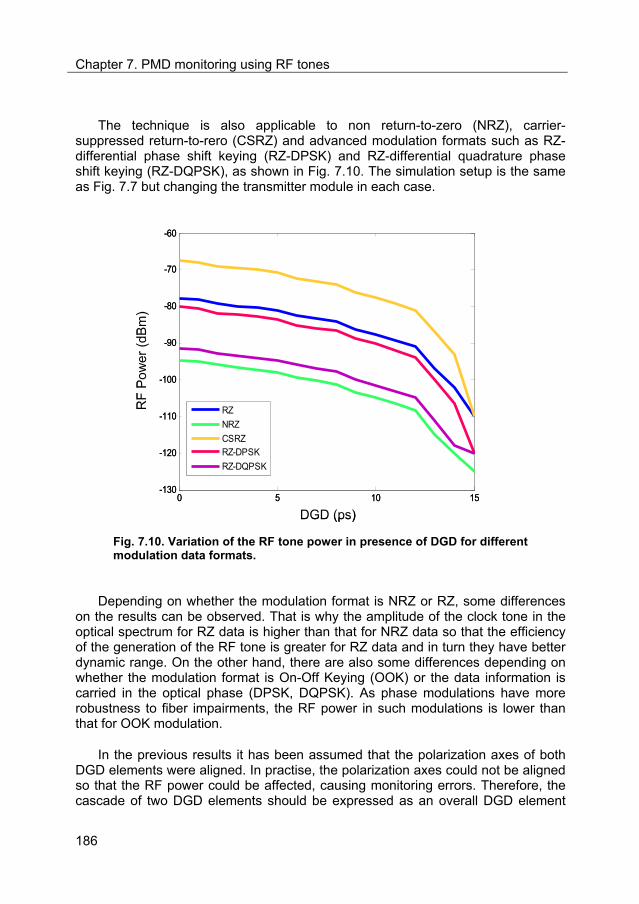
Chapter 7. PMD monitoring using RF tones
186
The technique is also applicable to non return-to-zero (NRZ), carrier-suppressed return-to-rero (CSRZ) and advanced modulation formats such as RZ-differential phase shift keying (RZ-DPSK) and RZ-differential quadrature phase shift keying (RZ-DQPSK), as shown in Fig. 7.10. The simulation setup is the same as Fig. 7.7 but changing the transmitter module in each case.
0 5 10 15-130
-120
-110
-100
-90
-80
-70
-60
DGD (ps)
RF
Pow
er (
dBm
)
RZ
NRZ
CSRZRZ-DPSK
RZ-DQPSK
DGD (ps)
RF
Pow
er(d
Bm
)
0 5 10 15-130
-120
-110
-100
-90
-80
-70
-60
DGD (ps)
RF
Pow
er (
dBm
)
RZ
NRZ
CSRZRZ-DPSK
RZ-DQPSK
DGD (ps)
RF
Pow
er(d
Bm
)
Fig. 7.10. Variation of the RF tone power in presence of DGD for different modulation data formats.
Depending on whether the modulation format is NRZ or RZ, some differences on the results can be observed. That is why the amplitude of the clock tone in the optical spectrum for RZ data is higher than that for NRZ data so that the efficiency of the generation of the RF tone is greater for RZ data and in turn they have better dynamic range. On the other hand, there are also some differences depending on whether the modulation format is On-Off Keying (OOK) or the data information is carried in the optical phase (DPSK, DQPSK). As phase modulations have more robustness to fiber impairments, the RF power in such modulations is lower than that for OOK modulation.
In the previous results it has been assumed that the polarization axes of both DGD elements were aligned. In practise, the polarization axes could not be aligned so that the RF power could be affected, causing monitoring errors. Therefore, the cascade of two DGD elements should be expressed as an overall DGD element

Chapter 7. PMD monitoring using RF tones
187
whose value depends on the coupling angle between these DGD components, as it will be explained in the next section.
7.3.3. Modelling of the cascade of two DGD elements
The Jones formalism, which describes the polarization states of polarized light, is used to model the cascade of two DGD elements and to obtain the overall DGD [Hec90, Cas94]. Concretely, the Jones formalism is based on the representation of the states of polarization by means of the amplitudes of the electrical field components and the phase difference between them. Then, the polarized light is represented by a Jones vector, and linear optical elements are represented by Jones matrix. When light passes through an optical element the resulting polarization of the emerging light is found by taking the product of the Jones matrix of the optical element and the Jones vector of the incident light.
Following this concept, the overall DGD is obtained by calculating the Jones matrix of the system composed of the first DGD element, a polarization rotator representing the coupling angle, and the second DGD component, Fig. 7.11.
Rotator
DGDEmulator
DGDoffset
21** DGDrotatorDGDtotal MMMM
Ein Eout
Rotator
DGDEmulator
DGDoffset
Rotator
DGDEmulator
DGDoffset
21** DGDrotatorDGDtotal MMMM
Ein Eout
Fig. 7.11. Modelling of the cascade of two DGD elements by means of Jones matrices.
The Jones matrices of the DGD elements and the rotator are given by [Pen99]:
1
1
1
exp 0
0 expDGD
j f DGDM
j f DGD
, (7.3)

Chapter 7. PMD monitoring using RF tones
188
anglecouplingtherepresentswhere
M Rotator
,cossin
sincos
(7.4)
2
2
2
exp 0
0 expDGD
j f DGDM
j f DGD
, (7.5)
and the system is represented by the multiplication of these three Jones matrices:
1 2
1
1
2
2
1 2 1 2
1 2 1 2
exp 0
0 exp
exp 0cos sin
0 expsin cos
cos exp( ) sin exp( )
sin exp( ) cos exp( )
total DGD rotador DGD
j fDGDM M M M
j fDGD
j fDGD
j fDGD
j f DGD DGD j f DGD DGD
j f DGD DGD j f DGD DGD
(7.6)
From the equations above, the intensity of the electric field at the output of the system can be calculated by using the following expression:
*out total inE M E , (7.7)
The phase delay between the electrical field components gives the overall DGD value experimented by the optical signal as a function of the coupling angle. In case of only considering the optical carrier, the phase delay is expressed as
2 1
1
exp 2 exp 2 * cos sin
cos exp 2 sin
y x
x y
j fDGD j fDGD E EPhase delay
E j fDGD E
, (7.8)
From (7.8), the maximum and the minimum overall DGD value depend on the coupling angle. When the coupling angle, , is 0º or 180º (i.e. the polarization axes of both elements are aligned), the overall DGD is equal to the sum of the DGD1 and DGD2. Conversely, when the coupling angle is 90º, a minimum overall DGD is obtained which is determined by the subtraction of the two DGD elements. The Table 7.1 summarizes the conclusions of this modelling.

Chapter 7. PMD monitoring using RF tones
189
Table 7.1. Overall DGD definition depending on the coupling angle.
Coupling Angle (Degree) Overall DGD
θ= 0º, 180º 1 2overallDGD DGD DGD
θ = 90º 1 2overallDGD DGD DGD
In case of considering not only the optical carrier but also the clock tone component, the resulting electrical field components are described by:
sidebandtotalcarriertotalt EMEME ** , where (7.9)
exp( 2 )
exp( 2 )cx c
carriercy c
E j f tE
E j f t
, and
exp( 2 )
exp( 2 )sx s
sidebandsy s
E j f tE
E j f t
,
being s c clockf f f
(7.10)
where fc is the frequency of the optical carrier, fclock is the frequency of the clock tone, and fs is the frequency of the new sideband. Ec,i and Es,i are the electric field components of the optical carrier and the sideband, respectively.
As before, the maximum overall DGD is obtained when both elements are aligned and corresponds to the sum of DGD1 and DGD2. The minimum overall DGD, however, is represented by the subtraction of the DGDs in cascade when the polarization axes are misaligned 90º. Then, to monitor PMD while taking into account the coupling angle, a polarization controller (PC) is scrambled in front of the large-DGD element for improving the sensitivity. To this end, in the simulations a polarization rotator is placed between both DGD elements and the coupling angle is swept from 0º to 180º. The polarization scrambling changes the input state of polarization in order to cover all the coupling angle possibilities. Later, the RF tone power (i.e. the maximum RF tone power, Pmax, and the minimum RF tone power, Pmin) is measured by an RF spectrum analyzer [Par02]. Fig. 7.12 shows the monitoring scheme with two DGD components in cascade and the PC scrambling. The parameters of the simulations are the same as before but including the sweep of the coupling angle.

Chapter 7. PMD monitoring using RF tones
190
40-Gb/sRZ data
DFBLaser
CDEmulator
PC
RF SpectrumAnalyzer
2.5-GHz
RxTransmitter
DGD Monitor
DGDoffsetDGD
EmulatorScrambling
PC40-Gb/sRZ data
DFBLaser
CDEmulator
PC
RF SpectrumAnalyzer
2.5-GHz
RxTransmitter
DGD Monitor
DGDoffsetDGD
EmulatorScrambling
PC
Fig. 7.12. Setup used for simulation study in the case of considering the coupling angle between the two DGD elements.
The modulated signal is polarization-scrambled so that the state of polarization of the data is rotated periodically before passing through the large-DGD element. Due to the PC scrambling, there are some coupling angle values whereby the state of polarization of the signal is aligned with one of the polarization axes so that the effect of PMD is completely eliminated. In this case, the detected RF power is maximized and this value is used for normalization, Pc [Lee01, Ono00]. On the other hand, the effect of PMD is maximized when the power of both principal polarization states is balanced (i.e., =0.5). In this case, the detected RF power can be then expressed as
2cosRF RF overall cP f DGD P , (7.11)
At this point, the overall DGD will be maximized when the polarization axes are aligned whereas it will be minimized for a misalignment of 90º. Then, depending on the overall DGD value, the measured optical power, PRF, varies periodically (i.e. from a maximum to a minimum value). Therefore, by measuring the maximum or the minimum detected power, the overall DGD can be estimated. As the large-DGD element is known, the DGD imposed by the fiber is monitored.
1 2
1 2
0º ,180º min
90º maxoverall RF
overall RF
DGD DGD DGD P
DGD DGD DGD P
, (7.12)
1cos (2 / 1)
2RF c
overallRF
P PDGD
f
, (7.13)
As expected from (7.13), the ratio between the maximum and the minimum power increases with PMD.
Simulation results show that for a given DGD value, the detected RF power varies between a maximum and a minimum value as a function of the coupling angle. Fig. 7.13 shows the RF power variation with the PC scrambling for different

Chapter 7. PMD monitoring using RF tones
191
DGD values. Note that these results are obtained by considering the ideal case, i.e. the DGD elements are aligned. As explained before, the minimum power is measured for coupling angles of 0º and 180º, whereas the maximum power appears with a misalignment of 90º. Then, by normalizing these values with respect to Pc (i.e., without PMD effect), both the overall DGD and the DGD of the fiber are calculated (using (7.13)). Table 7.2 shows the RF power corresponding to the coupling angle of 180º. From these values, the DGD can be monitored with accuracy better than ±1 ps.
Table 7.2. Estimated DGD of the fiber obtained by scrambling the PC when the polarization axes are aligned. (DGDOffset = 85 ps).
DGD Emulated
RF Power (dBm) DGDoverall =
DGDfiber+ DGDoffset Estimated DGDfiber
DGD= 0 ps 75 85 ps 0 ps
DGD= 5 ps 78.2 89.53 ps 4.53 ps
DGD= 12 ps 88 96.6 ps 11.6 ps
DGD= 15 ps 100 99.16 ps 14.16 ps
0 20 40 60 80 100 120 140 160 180-100
-95
-90
-85
-80
-75
-70
-65
-60
Angulo (grados)
Pot
enci
a de
RF
(dB
m)
DGD=0ps
DGD=5psDGD=12ps
DGD=15ps
Polarization axes aligned
RF
Pow
er
(dB
m)
Coupling angle (degrees)
DGDmin
DGDmax
2cos ( )RF RF overall cP f D GD Pmaxmin DGDpowerRF
minmax DGDpowerRF
0 20 40 60 80 100 120 140 160 180-100
-95
-90
-85
-80
-75
-70
-65
-60
Angulo (grados)
Pot
enci
a de
RF
(dB
m)
DGD=0ps
DGD=5psDGD=12ps
DGD=15ps
Polarization axes aligned
RF
Pow
er
(dB
m)
Coupling angle (degrees)
DGDmin
DGDmax
2cos ( )RF RF overall cP f D GD Pmaxmin DGDpowerRF
minmax DGDpowerRF
Fig. 7.13. RF power variation with the PC scrambling for different DGD values. The polarization axes are aligned.

Chapter 7. PMD monitoring using RF tones
192
Now, it is considered a misalignment between DGD components of 20º. In this case, the position of the maximum and the minimum RF powers are shifted to coupling angles 70º (90º 20º) and 160º (180º 20º), respectively (see Fig. 7.14). As before, the value of the DGD imposed by the fiber is estimated from the minimum detected power with an error of less than 1 ps. Table 7.3 shows the RF power corresponding to the coupling angle of 20º.
0 20 40 60 80 100 120 140 160 180-100
-95
-90
-85
-80
-75
-70
-65
-60
Angulo (grados)
Pot
enci
a de
RF
(dB
m)
DGD=0ps
DGD=5psDGD=12ps
DGD=15ps
Polarization misaligned (-20º)
Coupling angle (degrees)
DGDmin
DGDmax
RF
Pow
er
(dB
m)
0 20 40 60 80 100 120 140 160 180-100
-95
-90
-85
-80
-75
-70
-65
-60
Angulo (grados)
Pot
enci
a de
RF
(dB
m)
DGD=0ps
DGD=5psDGD=12ps
DGD=15ps
0 20 40 60 80 100 120 140 160 180-100
-95
-90
-85
-80
-75
-70
-65
-60
Angulo (grados)
Pot
enci
a de
RF
(dB
m)
DGD=0ps
DGD=5psDGD=12ps
DGD=15ps
Polarization misaligned (-20º)
Coupling angle (degrees)
DGDmin
DGDmax
RF
Pow
er
(dB
m)
Fig. 7.14. RF power variation with the PC scrambling for different DGD values. The polarization axes are misaligned (coupling angle= 20º).
Table 7.3. Estimated DGD of the fiber obtained by scrambling the PC when the polarization axes are misaligned (coupling angle= 20º). (DGDOffset = 85 ps).
DGD Emulated
RF Power (dBm) DGDoverall =
DGDfiber+ DGDoffset Estimated DGDfiber
DGD= 0 ps 76 84.75 ps 0.25 ps
DGD= 5 ps 79.2 89.5 ps 4.5 ps
DGD= 12 ps 89 96.6 ps 11.6 ps
DGD= 15 ps 100 99.05 ps 14.05 ps

Chapter 7. PMD monitoring using RF tones
193
Additionally, it should be noted that this technique can also be applied to other modulation formats such as NRZ, CS-RZ, RZ-DPSK and RZ-DQPSK, as commented in the case of not taking into account the coupling angle.
As said before, if the added optical carrier is placed inside the data bandwidth, it is difficult to recover it correctly. For this reason, the additional optical carrier is set out of band. However, it is highly desirable to put it in-band due to the following reasons: first, the transmitted signals can be distorted by the band-limiting caused by the cascading of optical filters [Kra08, Jia09]. Since the combined frequency response of the cascaded filters is the product of the individual frequency responses, the effective bandwidth is reduced as the number of cascaded filters is increased. Therefore, the presence of cascaded filters in the transmission links could affect and even filter the additional optical carrier. Second, for data recovery, a filter placed before the receiver is needed to suppress the optical carrier used for monitoring purposes. Owing to these drawbacks, a new DGD monitoring technique using an additional orthogonal shifted optical carrier is proposed.
7.4. DGD monitoring using an additional orthogonal shifted optical carrier
The proposed first-order PMD monitoring technique is also based on adding an additional optical carrier shifted with respect to the data carrier, but at the orthogonal polarization state in order to be in-band with the data and not to affect their recovery. As before, after detection, the added carrier beats with the upper and lower clock tones of the data generating beat signals at frequencies Rb ± fshift (Rb is the bitrate and fshift is the shift between the data carrier and the additional carrier), whereby the resulting RF power of these beat signals depends on the PMD value.
7.4.1. Description of the DGD monitoring technique
The first-order PMD causes different propagation velocities for the signal travelling on two orthogonal states of polarization. Due to DGD, the polarization states of the both clock tones are rotated ±θ degrees with respect to the optical carrier. The rotation is given by:
2 f DGD , (7.14)
where f is the frequency difference between the clock tones and the optical
carrier [Nel99].

Chapter 7. PMD monitoring using RF tones
194
Thus, without DGD, the rotation is equal to zero; so that the clock tones and the optical carrier remain orthogonal resulting in no beat RF tones at the receiver. Conversely, the DGD depolarizes the clock tones and the optical carrier increasing the power of the beat RF tones significantly. In addition, by placing the added optical carrier close to the clock tone, a very low-frequency beat tone (i.e. Rb fshift tone) can be selected, and used for DGD monitoring of high-speed data with a low-speed detector, providing a cost-effective solution. A conceptual diagram of the proposed technique is illustrated in Fig. 7.15. On the other hand, since the upper and lower optical clock tones are asymmetric with the added shifted carrier, accurate CD-insensitive DGD monitoring is performed.
RbRb
Added carrier
fshift
DGD
Rb - fshift
Rb + fshift
Rb
Freq (GHz)
Depolarization
RbRb
Added carrier
fshift
DGDDGD
Rb - fshift
Rb + fshift
Rb
Freq (GHz)
Depolarization
Fig. 7.15. Conceptual diagram of the PMD monitoring technique based on adding an additional optical carrier at the orthogonal polarization.
7.4.2. Simulation results
The proposed PMD monitoring technique is validated by means of simulations using the Virtual Photonics Inc. software. Fig. 7.16 shows the scheme used for DGD monitoring.
40-Gb/sRZ data
DFBLaser
PC
PBC
PC
DGDEmulatorPC
RF SpectrumAnalyzer
2.5-GHz
Rx
Transmitter
DGD Monitor
40-Gb/sRZ data
DFBLaser
PC
PBC
PC
DGDEmulatorPC
RF SpectrumAnalyzer
2.5-GHz
Rx
Transmitter
DGD Monitor
Fig. 7.16. Setup used for simulation study.

Chapter 7. PMD monitoring using RF tones
195
At the transmitter, a 40-Gbit/s RZ signal is generated by using the VPI Tx Pulse module. Using this module a modulated RZ pulse signal with FWHM of 5 ps is generated. Then, an additional DFB laser is combined with the data using a polarization beam combiner (PBC), placing it in the orthogonal polarization state. The frequency difference between both optical carriers is around 37.5 GHz to generate a low-frequency tone which is measured for PMD estimation. The peak power of both lasers is set to 1 mW. The DGD monitor consists of a low-speed detector (2.5-GHz) followed by an RF spectrum analyzer.
First of all, the performance of the received data is tested. As shown in Fig. 7.17 , even in presence of the shifted carrier, a clear diagram is obtained.
OPTICAL SPRECTRUM EYE DIAGRAM
Optical frequency related to 193.1 THz (GHz) Time (ps)
a) b)
OPTICAL SPRECTRUM EYE DIAGRAM
Optical frequency related to 193.1 THz (GHz) Time (ps)
a) b)
Rb Rb
Added carrier
fshift
OPTICAL SPRECTRUM EYE DIAGRAM
Optical frequency related to 193.1 THz (GHz) Time (ps)
a) b)
OPTICAL SPRECTRUM EYE DIAGRAM
Optical frequency related to 193.1 THz (GHz) Time (ps)
a) b)
Rb Rb
Added carrier
fshift
Fig. 7.17. a) optical spectrum showing the data together with the added optical carrier placed in-band; b) Eye diagram of the received data.
Fig. 7.18 shows the response of the RF power in the presence of DGD for RZ and RZ-DPSK, obtaining an RF power increment around 20 dB in the DGD range from 0 to 25 ps. The DGD is emulated as explained in the previous section. Note that, in this case, the technique is quite sensitive for low values of DGD which is very interesting for high-speed data monitoring.

Chapter 7. PMD monitoring using RF tones
196
0 5 10 15 20 25
-120
-110
-100
-90
-80
-70
-60
RF
Pow
er
(dB
m)
DGD (ps)
RZ
RZ-DPSK
RF
Pow
er(d
Bm
)
DGD (ps)
0 5 10 15 20 25
-120
-110
-100
-90
-80
-70
-60
RF
Pow
er
(dB
m)
DGD (ps)
RZ
RZ-DPSK
0 5 10 15 20 25
-120
-110
-100
-90
-80
-70
-60
RF
Pow
er
(dB
m)
DGD (ps)
RZ
RZ-DPSK
RZ
RZ-DPSK
RF
Pow
er(d
Bm
)
DGD (ps)
Fig. 7.18. RF power response as a function of the DGD for RZ and RZ-DPSK data formats.
As a remark, the technique is also applicable to NRZ, CSRZ and advanced modulation formats such as RZ-DQPSK.
7.4.3. Experimental results
Once validated the proposed DGD monitoring technique by means of simulations, the experimental demonstration of the method for 40-Gbit/s RZ data is performed by the setup shown in Fig. 7.19. At the transmitter, a continuous-wave laser at 1551.7 nm is externally modulated by a 40-GHz intensity modulator and then an RZ pulse carver driven by a 20-GHz clock source generates the 40-Gbit/s RZ signal. An additional DFB laser at 1552.005 nm is combined with the data using a polarization beam combiner (PBC) so that they are in orthogonal polarization states. The frequency difference between both optical carriers is around 38 GHz. The signals are then coupled with amplified spontaneous emission (ASE) noise to adjust the OSNR values. These channels are then passed through the tunable CD and DGD emulators. The DGD monitor consists of a low-speed detector (2.5-GHz) and an RF spectrum analyzer. The RF power at low frequency content (i.e. Rb fshift ~ 2 GHz) is measured for DGD monitoring.

Chapter 7. PMD monitoring using RF tones
197
ASESource40-Gb/s
RZ data
DFBLaser
PC
PBC
PC
CDEmulator
DGDEmulatorPC
RF SpectrumAnalyzer
2.5-GHz
Rx
Transmitter
DGD Monitor
ASESource40-Gb/s
RZ data
DFBLaser
PC
PBC
PC
CDEmulator
DGDEmulatorPC
RF SpectrumAnalyzer
2.5-GHz
Rx
Transmitter
DGD Monitor
Fig. 7.19. Experimental setup.
First, the principle of operation is tested, observing a minimum RF power when no DGD is present. In contrast, as PMD increases, the RF power increases as well. Fig. 7.20 shows the RF power for DGD values of 0 and 80 ps. The 80-ps DGD value has been obtained by using a fiber span of polarization-maintaining fiber (PM fiber) characterized to introduce such DGD value. An RF power difference of more than 20 dB is obtained.
1.5 1.6 1.7 1.8 1.9 2 2.1-60
-55
-50
-45
-40
RF
Pow
er(d
Bm
)
Frequency (GHz)
DGD=0 ps
DGD= 80 ps
1.5 1.6 1.7 1.8 1.9 2 2.1-60
-55
-50
-45
-40
RF
Pow
er(d
Bm
)
Frequency (GHz)
DGD=0 ps
DGD= 80 ps
Fig. 7.20. RF power for DGD values of 0 and 80 ps. In presence of PMD the power of the RF tone increases dramatically.
After that, to optimize the generation of the RF tone due to the PMD for a specific PMD value, it is analyzed how the ratio between both optical carriers
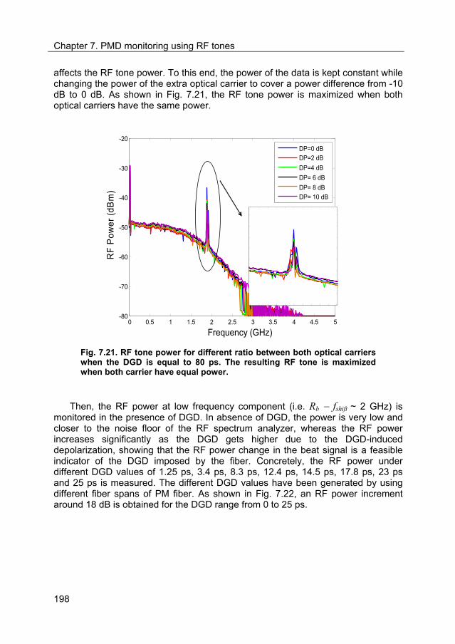
Chapter 7. PMD monitoring using RF tones
198
affects the RF tone power. To this end, the power of the data is kept constant while changing the power of the extra optical carrier to cover a power difference from -10 dB to 0 dB. As shown in Fig. 7.21, the RF tone power is maximized when both optical carriers have the same power.
0 0.5 1 1.5 2 2.5 3 3.5 4 4.5 5-80
-70
-60
-50
-40
-30
-20
Frecuencia (GHz)
Pot
enc
ia (
dBm
)
DP=0 dB
DP=2 dB
DP=4 dB
DP= 6 dB
DP= 8 dB
DP= 10 dB
0 0.5 1 1.5 2 2.5 3 3.5 4 4.5 5-80
-70
-60
-50
-40
-30
-20
Frequency (GHz)
RF
Pow
er(d
Bm
)
DP=0 dB
DP=2 dB
DP=4 dB
DP= 6 dB
DP= 8 dB
DP= 10 dB
0 0.5 1 1.5 2 2.5 3 3.5 4 4.5 5-80
-70
-60
-50
-40
-30
-20
Frecuencia (GHz)
Pot
enc
ia (
dBm
)
DP=0 dB
DP=2 dB
DP=4 dB
DP= 6 dB
DP= 8 dB
DP= 10 dB
0 0.5 1 1.5 2 2.5 3 3.5 4 4.5 5-80
-70
-60
-50
-40
-30
-20
Frecuencia (GHz)
Pot
enc
ia (
dBm
)
DP=0 dB
DP=2 dB
DP=4 dB
DP= 6 dB
DP= 8 dB
DP= 10 dB
0 0.5 1 1.5 2 2.5 3 3.5 4 4.5 5-80
-70
-60
-50
-40
-30
-20
Frequency (GHz)
RF
Pow
er(d
Bm
)
DP=0 dB
DP=2 dB
DP=4 dB
DP= 6 dB
DP= 8 dB
DP= 10 dB
Fig. 7.21. RF tone power for different ratio between both optical carriers when the DGD is equal to 80 ps. The resulting RF tone is maximized when both carrier have equal power.
Then, the RF power at low frequency component (i.e. Rb fshift ~ 2 GHz) is monitored in the presence of DGD. In absence of DGD, the power is very low and closer to the noise floor of the RF spectrum analyzer, whereas the RF power increases significantly as the DGD gets higher due to the DGD-induced depolarization, showing that the RF power change in the beat signal is a feasible indicator of the DGD imposed by the fiber. Concretely, the RF power under different DGD values of 1.25 ps, 3.4 ps, 8.3 ps, 12.4 ps, 14.5 ps, 17.8 ps, 23 ps and 25 ps is measured. The different DGD values have been generated by using different fiber spans of PM fiber. As shown in Fig. 7.22, an RF power increment around 18 dB is obtained for the DGD range from 0 to 25 ps.

Chapter 7. PMD monitoring using RF tones
199
0 5 10 15 20 25-66
-64
-62
-60
-58
-56
-54
-52
-50
-48
RF
Pow
er(d
Bm
)
DGD (ps)0 5 10 15 20 25
-66
-64
-62
-60
-58
-56
-54
-52
-50
-48
RF
Pow
er(d
Bm
)
DGD (ps)
Fig. 7.22. RF power response as a function of DGD.
Additionally, the RF power under different CD values of 0 ps/nm, 160 ps/nm, 440 ps/nm and 860 ps/nm is measured, detecting a variation of less than 1 dB as shown in Fig. 7.23. The CD values have been generated by using different single-mode (SMF) fiber spans with a dispersion parameter of 17 ps/nm.km. The length of these SMF fiber spans are 9.4 km, 25.8 km, and 50.5 km, respectively. Also, the performance of the technique while changing the OSNR value is tested. The OSNR value can be adjusted from 15 to 25 dB by combining the signal with an ASE noise source at different power levels to emulate different OSNR scenarios. As shown in Fig. 7.24, the RF tone power is also insensitive to OSNR.

Chapter 7. PMD monitoring using RF tones
200
0.5 1 1.5 2 2.5 3
-65
-60
-55
-50
-45
Frequency (GHz)
RF
Pow
er(d
Bm
)
DL= 0ps/nmDL= 160ps/nmDL= 440ps/nmDL= 860ps/nm
PMD= 23 ps
0.5 1 1.5 2 2.5 3
-65
-60
-55
-50
-45
Frequency (GHz)
RF
Pow
er(d
Bm
)
DL= 0ps/nmDL= 160ps/nmDL= 440ps/nmDL= 860ps/nm
0.5 1 1.5 2 2.5 3
-65
-60
-55
-50
-45
Frequency (GHz)
RF
Pow
er(d
Bm
)
DL= 0ps/nmDL= 160ps/nmDL= 440ps/nmDL= 860ps/nm
PMD= 23 ps
Fig. 7.23. RF power under different CD values (0 ps/nm, 160 ps/nm, 440 ps/nm, 860 ps/nm) for a DGD of 23 ps.
0.5 1 1.5 2 2.5 3
-80
-75
-70
-65
-60
-55
-50
-45
-40
-35
-30
Po
tenc
ia (
dBm
)
Frecuencia (GHz)
OSNR= 15 dB
OSNR= 17 dB
OSNR= 19 dB
OSNR= 21 dB
OSNR= 23 dB
OSNR= 25 dB
0.5 1 1.5 2 2.5 3
-80
-75
-70
-65
-60
-55
-50
-45
-40
-35
-30
RF
Pow
er(d
Bm
)
Frequency (GHz)
OSNR= 15 dB
OSNR= 17 dB
OSNR= 19 dB
OSNR= 21 dB
OSNR= 23 dB
OSNR= 25 dB
PMD= 23 ps
0.5 1 1.5 2 2.5 3
-80
-75
-70
-65
-60
-55
-50
-45
-40
-35
-30
Po
tenc
ia (
dBm
)
Frecuencia (GHz)
OSNR= 15 dB
OSNR= 17 dB
OSNR= 19 dB
OSNR= 21 dB
OSNR= 23 dB
OSNR= 25 dB
0.5 1 1.5 2 2.5 3
-80
-75
-70
-65
-60
-55
-50
-45
-40
-35
-30
RF
Pow
er(d
Bm
)
Frequency (GHz)
OSNR= 15 dB
OSNR= 17 dB
OSNR= 19 dB
OSNR= 21 dB
OSNR= 23 dB
OSNR= 25 dB
0.5 1 1.5 2 2.5 3
-80
-75
-70
-65
-60
-55
-50
-45
-40
-35
-30
Po
tenc
ia (
dBm
)
Frecuencia (GHz)
OSNR= 15 dB
OSNR= 17 dB
OSNR= 19 dB
OSNR= 21 dB
OSNR= 23 dB
OSNR= 25 dB
0.5 1 1.5 2 2.5 3
-80
-75
-70
-65
-60
-55
-50
-45
-40
-35
-30
Po
tenc
ia (
dBm
)
Frecuencia (GHz)
OSNR= 15 dB
OSNR= 17 dB
OSNR= 19 dB
OSNR= 21 dB
OSNR= 23 dB
OSNR= 25 dB
0.5 1 1.5 2 2.5 3
-80
-75
-70
-65
-60
-55
-50
-45
-40
-35
-30
RF
Pow
er(d
Bm
)
Frequency (GHz)
OSNR= 15 dB
OSNR= 17 dB
OSNR= 19 dB
OSNR= 21 dB
OSNR= 23 dB
OSNR= 25 dB
PMD= 23 ps
Fig. 7.24. RF power under different OSNR values (from 15 to 25 dB) for a DGD of 23 ps.

Chapter 7. PMD monitoring using RF tones
201
Finally, the technique is validated using the generation of a RF tone in the MHz range. Fig. 7.25 shows that the RF tone appears when DGD is present, although the dynamic range is reduced by some decibels.
0 0.5 1 1.5 2 2.5 3 3.5 4 4.5 5-80
-70
-60
-50
-40
-30
-20
Frequency (GHz)
RF
Pow
er(d
Bm
)
f = 1.6 GHz
f = 450 MHz
0 0.5 1 1.5 2 2.5 3 3.5 4 4.5 5-80
-70
-60
-50
-40
-30
-20
Frequency (GHz)
RF
Pow
er(d
Bm
)
f = 1.6 GHz
f = 450 MHz
Fig. 7.25. RF power under a DGD value of 23 ps when the RF tone appears at very low frequency (~ MHz).
7.5. Summary and conclusions
The future dynamically reconfigurable optical networks based on packet traffic have provided the main driver to develop new techniques for optical performance monitoring with fast response and on a packet-by-packet basis. Ideally, a single monitor should allow the independent measurement of physical degradations providing a cost effective solution. In particular, PMD is notably critical for next generation high bitrate optical networks.
Given the stochastic nature of PMD, it is desirable to monitor PMD in order to dynamically tune a compensator and also to isolate the PMD effects from other physical impairments such as CD. Several PMD monitoring techniques based on RF spectrum measurements have been reported in the literature, but these techniques have some disadvantages that limit their applicability in OPS networks.
In this Chapter, two clock-tone-based PMD monitoring techniques have been presented. The major advantage of the proposed techniques is that they allow independent PMD monitoring as well as providing a cost-effective solution even with high-speed data.
Chapter 7. PMD monitoring using RF tones
202
Instead of inserting a monitoring-field into the optical header for monitoring as in the previous techniques presented in this Thesis, these techniques use the RF spectrum of the whole packet. The concept of using the RF spectrum of one packet to perform the monitoring on a packet basis has been validated by simulations. In fact, the simulations have confirmed the applicability of the pilot-tone-based techniques in OPS networks. Synchronization is provided by the optical packet switching node. Moreover, by using fast RF power detectors, response times could be around ns. Regarding measurement sensitivity, a simulation study has been carried out, showing that for packet length longer than 500 bytes the dynamic range is appropriate for such networks.
Both proposed techniques are based on adding a new optical carrier shifted with respect to the data carrier to generate new RF tone at very low-frequencies. The first technique described in this Chapter adds an extra DGD element, DGDoffset, to increase the sensitivity of the measurement, allowing reliable PMD monitoring with low-speed detectors. The cascade of DGD elements has been modelled by the Jones formalism taking into the account the coupling angle between them. The simulation results derived from the modelling show that the PMD imposed by the fiber can be estimated with an accuracy better than ±1 ps and the measurement is CD-insensitive. However, the fact of placing the added optical carrier out-of-band to properly recover the data introduces some drawbacks which the second proposed technique overcomes.
The second proposed technique is also based on adding a new optical carrier, but this time at the orthogonal polarization state. This means that the extra optical carrier can be placed in-band without affecting the data recovery. The proposed architecture has been tested by means of simulations as well as experimentally validated, confirming the successful monitoring operation. An RF power range of 18 dB is obtained for the DGD range from 0 to 25 ps. Furthermore, the measurements are insensitive to CD and to OSNR as well, observing power variations of less than 1 dB. Finally, the monitoring principle with generated clock tones at a frequency of MHz has also been presented.

Chapter 7. PMD monitoring using RF tones
203
7.6 References
[Bin02] C. Bintjas, N. Pleros, K. Yiannopoulos, G. Theophilopoulos, M. Kalyvas, H. Avramopoulos, and G. Guekos, “All-optical packet address and payload separation,” IEEE Photon. Technol. Lett., vol. 14, no. 12, pp. 1728–1730, Dec. 2002.
[Cas94] J. Casas, “Optica”, Lib. Pons, 1994.
[Chu00] H.S. Chung, S.K. Shin, K.J. Park, H.G. Woo, and Y.C. Chung, “Effects of stimulated Raman scattering on pilot-tone-based supervisory technique,” IEEE Photonics Technol. Lett., vol. 12, no. 6, pp. 731–733, 2000.
[Hec90] E. Hecht, and A. Zajac, “Optica,” Ed. Addison Wesley Iberoamricana, 1990.
[Ishi98] G. Ishikawa, and H. Ooi, “Polarization-mode dispersion sensitivity and monitoring in 40-Gbit/s OTDM and lO-Gbit/s NRZ transmission experiments,” in Proc. of Optical Fiber Communication Conference (OFC’98), San Jose (CA, USA), paper WC5, 1998.
[Ji04] H.C. Ji, “Optical Performance monitoring techniques based on pilot tones for WDM network applications”, J. Optical Networking, vol. 3, no. 7, pp. 510-533, 2004.
[Jia09] Y. Jiang, X. Tang, J.C. Cartledge, and K. Roberts, “Pre-compensation for the Effects of Cascaded Optical Filtering on 10 Gsymbol/s DPSK and DQPSK Signals,” in Proc. of 35th European Conference on Optical Communications (ECOC’09), Vienna (Austria), paper P4.14, 2009.
[Kra08] D. Krause, Y. Jiang, J.C. Cartledge, and K. Roberts, “Precompensation for narrow optical filtering of 10-Gbit/s intensity modulated signals,” IEEE Photon. Technol. Lett., vol. 20, no. 9, pp. 706-708, 2008.
[Lee01] J.H. Lee, D.K. Jung, C.H. Kim, and Y.C. Chung, “OSNR monitoring technique using polarization-nulling method,” IEEE Photonics Technol. Lett., vol. 13, no. 1, pp. 88–90, 2001.
[Liz06] Y.K. Lize, “Simultaneous Monitoring of Chromatic Dispersion and PMD for OOK and DPSK Using Partial-Bit-Delay-Assisted Clock Tone Detection,” in 32nd European Conference on Optical Communications (ECOC’06), Cannes (France), paper Mo4.4.7, 2006.
[Lu05] G.W. Lu, M.H. Cheung, L.K. Chen, and C.K. Chan, “Simultaneous PMD and OSNR Monitoring by Enhanced RF Spectral Dip Analysis Assisted With a Local Large-DGD Element,” IEEE Photon. Technol. Lett., vol. 17, no. 12, pp. 2790-2792, 2005.
[Nel99] L.E. Nelson, “Measurement of depolarization and scaling associated with

Chapter 7. PMD monitoring using RF tones
204
second-order polarization mode dispersion in optical fibers”, IEEE Photon. Technol. Lett., vol. 11, no. 12, pp. 1614-1616, 1999.
[Nez01] S.M.R.M. Nezam, Y.Wang, M. Hauer, S. Lee, and A.E.Willner, “Simultaneous PMD monitoring of several WDM channels using subcarrier tones,” in Proc. of Conference on Lasers and Electro-Optics (CLEO’01), Baltimore (Maryland, USA), vol. 56, pp. 561-562, 2001.
[Nez04a] S.M.R.M. Nezam, J.E. McGeehan, and A.E. Willner, “Measuring fiber and component DGD using polarized limited-bandwidth optical sources and monitoring the DOP,”IEEE Photon. Technol. Lett., vol. 16, no. 7, pp. 1694-1696, 2004.
[Nez04b] S.M.R.M. Nezam, Y.W. Song, C. Yu, J.E. McGeehan, A.B. Sahin, and A.E. Willner, “First-Order PMD Monitoring for NRZ Data Using RF Clock Regeneration Techniques,” IEEE/OSA J. Lightwave Technol., vol. 22, no. 4, pp. 1086–1093, 2004.
[Ono00] T. Ono, Y. Yano, L.D. Garrett, J.A. Nagel, M.J. Dickerson, and M. Cvijetic, “10 Gbit/s PMD compensation field experiment over 452 km using principle state transmission method,” in Proc. of Optical Fiber Communication Conference (OFC’00), Baltimore (Maryland, USA), paper PD44.
[Par02] K.J. Park, J.H. Lee, C.J. Youn, and Y.C. Chung, “A simultaneous monitoring technique for polarization-mode dispersion and group-velocity dispersion,” in Proc. of Optical Fiber Communication Conference (OFC’02), Anaheim (CA, USA), WE4, pp. 199–200, 2002.
[Pen99] D. Penninckx, and V. Morenas, “Jones matrix of polarization mode dispersion,” Opt. Letters, vol. 24, no. 13, pp. 875-877, 1999.
[Ros00] G. Rossi, T.E. Dimmick, and D.J. Blumenthal, “Optical performance monitoring in reconfigurable WDM optical networks using subcarrier multiplexing,” IEEE/OSA J. Lightwave Technol., vol. 18, no. 12, pp. 639–1648, 2000.
[Sun97] Y. Sun, A.A.M. Saleh, J.L. Zyskind, D.L. Wilson, A.K. Srivastava, and J.W. Sulhoff, “Time dependent perturbation theory and tones in cascaded erbium-doped fiber amplifier systems,” IEEE/OSA J. Lightwave Technol., vol. 15, no. 7, pp. 1083–1087, 1997.
[Sun02] H. Sunnerud, M. Karlsson, X. Chongjin, P.A. Andrekson, “Polarization-mode dispersion in high-speed fiber-optic transmission systems”, IEEE/OSA J. Lightwave Technol., vol. 20, no. 12, pp. 2204-2219, 2002.
[Yas03] M. Yasin Akhtar Raja and S. K. Arabasi, “Design and simulations of a dynamic polarization-mode dispersion compensator for long-haul optical networks,” Optics Express, vol. 11, no. 10, pp. 1166-1174, 2003.
[Yi06] X.Yi, W. Chen, and W. Shieh, “An OSNR monitor for optical packet switched

Chapter 7. PMD monitoring using RF tones
205
networks,” IEEE Photon. Technol. Lett., vol. 18, no. 13, pp. 1448-1450, 2006.


207
Chapter 8
Conclusions and future work
8.1. Introduction
In this Thesis, two key topics have been addressed. The first one has dealt with the design of an all-optical packet-switched network and the definition of migration scenarios from the current optical circuit-switched (OCS) networks towards future optical packet-switched networks (OPS). The proposed migration strategies are based on hybrid networks which combine different types of switching technologies. The second and main topic has been focused on how to perform optical performance monitoring (OPM) in the frame of OPS networks.
In this Chapter, the contributions and the main conclusions of this Thesis are summarized, and recommendations for future work are also given.
8.2. Summary of the work
Optical networks are evolving towards all-optical solution to avoid the bottleneck imposed by electronic processing. All-optical label switching (AOLS) technologies are believed to be key for increasing the throughput of future OPS networks and have been proposed as a viable approach to resolve the mismatch between fiber transmission capacity and router packet forwarding capacity [Blu00, Lis00].

Chapter 8. Conclusions and future work
208
In this context, two possible network architectures based on the AOLS concept have been proposed. The former approach consists of a pure packet-switched network where OPS nodes are connected directly using WDM links. The second approach is based on a mixed packet-circuit solution where packet nodes are connected using circuits provided by the circuit layer. In both architectures two node functionalities (core and edge functionalities) have been addressed.
Although the all-optical architecture is particularly beneficial for transparent high-speed packet switching and forwarding, the deployment of a truly all-optical network is expected to be a reality in the long term [Cae06]. Awaiting for this new network, hybrid network architectures must be defined. In this Thesis, several migration scenarios based on hybrid OCS/OBS/OPS technologies have been proposed. In the node per node strategy, there is a gradual replacement of the existing network nodes with the nodes of the future network. Of course interfaces should be foreseen so that the different nodes can communicate and traffic throughput is guaranteed. The island based migration is a similar approach but now sub-networks of the future network are introduced in the original network. Also mixed network scenarios have been proposed. It has been differentiated between the ORION approach in which the idle periods on optical circuits are filled with overspill packets to reduce the packet loss and the OPS scenario with underlying OCS. In the latter scenario OCS provides the light path connections to transport the packets. Among all the scenarios presented, an architecture integrating completely two network technologies optimizes the overall network operation since the resulting architecture shares the same bandwidth resources in the same network simultaneously. However, this implies an increase in the complexity. Hence, a more realistic and feasible approach consists of an OCS layer and an OPS layer in parallel. In such a solution, an intelligent edge node employs the different network technologies individually, or in combination, in order to optimally serve customer service requirements.
Emerging services such as voice-over-IP, video streaming, and high definition TV demand stringent network requirements in terms of latency, data integrity, and availability [Cae07]. Such requirements are very important from a network operator’s perspective because if fulfilled, they enable the operator to deliver guaranteed services to different types of user groups. Hence, it is desirable to include additional functionalities responsible of performance monitoring and fault management inside the intermediate nodes of future optical networks [Tei09]. In this Thesis, the design of the optical network architectures considers the integration between the control plane and management plane so that the network nodes perform new functions, intimately correlated with performance monitoring and recovery schemes.
Given the increasing interest in optical OPM, in this Thesis it has been investigated how to perform signal quality monitoring in OPS networks. Such networks bring about new challenges to the research in OPM since the monitoring must be done on a packet-by-packet basis. In this Thesis, all-optical approaches

Chapter 8. Conclusions and future work
209
for OPM in OPS networks have been presented. These techniques are based on using a specific word (monitoring field, Q-field) inserted into the packet header which is processed in each intermediate node for monitoring purposes. Thus, when the packet arrives at the node, it enters into a circuit responsible of extracting the monitoring field and the signal quality of the incoming packet is estimated later from the extracted Q-field [Stam05]. The main conclusions related to OPM are summarized below.
A novel OSNR monitoring technique based on optical correlation has been proposed. The monitoring field suffering from impairments imposed by the network links is correlated with an undegraded version of this reference signal. As a result, the degree of degradation can be extracted from amplitude statistics of the autocorrelation pulse produced at the correlator output. In fact, by using the noise statistics of the autocorrelation pulse peak power, the OSNR of the incoming packets can be calculated.
To experimentally verify the proposed OSNR monitoring technique, an optical correlator based on fiber Bragg gratings (FBG) has been fabricated [Hau03]. Experimental results show that for an OSNR in the range of 15 dB to 25 dB the OSNR can be estimated with an error lower than 0.5 dB. The advantages of the technique using optical correlator are in-band ASE noise measurements, quality signal estimation with relaxed speed requirements with respect to typical sampling techniques, and simple implementation. Furthermore, the following practical applications of the proposed OSNR monitor have been presented:
1. The OSNR monitor could be deployed as part of QoS to ensure that packets are properly treated along the network according to their QoS level.
2. The monitoring information obtained from the optical monitor could be included when calculating new routes for data signals. Indeed, signal quality monitoring information could be added as an additional factor in the routing decision in order to keep the level of QoS promised to customers.
3. The OSNR information could be utilized for path monitoring for restoration functions.
Moreover, a DGD monitoring technique based on a logic XOR gate implemented in an integrated SOA-MZI has been presented. The monitoring system consists of a XOR-based DGD monitor and an all-optical 1x2 packet switch. The DGD monitor detects the delay differences that the two orthogonal states of polarization of the signal suffer along the fiber, obtaining an increment of the XOR output power as DGD increases. The output of the XOR gate acts as the control signal for the optical switch, which operates in a similar way to an optical flip-flop. Hence, when the XOR gate estimates a large DGD, the input packet is

Chapter 8. Conclusions and future work
210
switched to the dropping port of the switch to reduce the network traffic load. This operation leads to the possibility of taking real-time routing decisions and in-line PMD compensation.
The architecture has been tested by simulations, showing the proper operation of the proposed technique. Furthermore, experimental results have been carried out to demonstrate the XOR-based monitoring subsystem, obtaining similar behaviour to the simulation results. Although the DGD monitoring technique has been experimentally validated at 10 Gbit/s, it may be also extended to higher bitrates by using a differential scheme placed at the input of the XOR gate [Web03]. Furthermore, the proposed scheme allows real-time DGD monitoring at the optical domain, offering a promising solution due to its simplicity, scalability, and integration capability.
On the other hand, the concept of the “time-to-live” (TTL) field within the label of a packet originated from IP networks has been used for monitoring purposes. Every time a packet goes through one hop in the network its quality is reduced. So the maximum degradation that a packet can support matches a maximum number of router hops (TTL value). Then, the monitoring technique operates as follows. If the value of the TTL field within the packet is nonzero, the TTL is decremented and the packet passes through the module. If the TTL field is zero, however, the module generates a signal that can be used to drop the packet or send it to a regeneration element.
An all-optical TTL subtractor has been implemented with the cascade of two SOA-MZI devices acting as logic XOR gates and a 1-binary subtraction algorithm based on decrementing via inversion has also been defined. The proposed TTL decrementing technique has been tested by simulations to demonstrate the subtraction operation employing practical devices. Simulation results at 10 Gbit/s show the feasibility of the proposed scheme. The performance of the architecture has been assessed by using the extinction ratio, obtaining values higher than 10 dB. Furthermore, in order to validate the cascading functionality, the Q-factor has been measured at the output of the subtractor for several recursive operations. The results show that the Q-factor is reduced by increasing the number of bits, mainly due to ASE noise introduced by the SOAs. Obviously, the maximum number of subtractions (TTL field initial value) depends on specific parameters of the SOA-MZI devices and the ASE noise generated [Yu01]. This technique is independent of the length of the TTL and packet, demands no electronic control, and requires no guard time between the end of the TTL field and the rest of the packet. Moreover, the TTL concept can be used to provide service-differentiation functionalities.
Apart from the proposed all-optical monitoring techniques, in this Thesis some concepts derived from the RF-spectrum-based monitoring techniques have been extended for their applicability to OPS networks. In fact, two PMD monitoring techniques based on RF spectrum measurements have been proposed. The main
Chapter 8. Conclusions and future work
211
features of both techniques are that they perform the monitoring on a packet basis and they provide a cost-effective solution appropriate for high-speed networks. On the other hand, instead of inserting a monitoring-field into the optical header for monitoring as in the proposed techniques presented previously, these techniques use the RF spectrum of the whole packet for the sake of a better sensitivity.
Both proposed techniques are based on adding a new optical carrier shifted with respect to the data carrier to generate a new RF tone at very low-frequencies. The first technique described adds an extra DGD element to increase the sensitivity of the measurement, allowing reliable PMD monitoring with low-speed detectors. The cascade of two DGD elements has been modelled by the Jones formalism taking into account the coupling angle between them. The simulation results derived from the defined modelling show that the PMD imposed by the fiber can be estimated with accuracy better than ±1ps and the measurement is CD-insensitive. However, the fact of placing the added optical carrier out-of-band to properly recover the data introduces some drawbacks which are overcome with the second proposed technique.
The second proposed technique is also based on adding a new optical carrier, but this time at the orthogonal polarization state. This means that the extra optical carrier can be placed in-band without affecting the data recovery. The proposed architecture has been tested by means of simulations, and experimentally validated, confirming the successful monitoring operation. An RF increment of 18 dB is obtained for the DGD range from 0 to 25 ps. Furthermore, the measurements are insensitive to CD and to OSNR as well, observing power variations of less than 1 dB.
8.3. Future work
Once finished this Thesis, there are several issues related to the topic of OPM in OPS networks that remain opened. Possible extensions of the work performed are proposed in this section.
In the proposed OSNR monitoring technique presented in Chapter 4, the FBG-based correlator was designed with unequal grating spacing, i.e. with different time intervals. By means of simulations, a study of the correlator output as function of the pattern written into the FBG array was carried out in order to decide which one provided better performance and less overhead. At this point, the pattern can be also chosen to improve the auto/cross-correlation properties. This means that the proper selection of codes with special properties can lead to an increase in the difference between the autocorrelation output and the cross-correlation outputs, allowing the provision of QoS applications. In the literature, longer and sparser aperiodic Quadratic

Chapter 8. Conclusions and future work
212
(QC) and Extended Quadratic Congruence (EQC) codes have been used because they have better performances than other typical codes [Mar93]. Experiments using QC and EQC codes for the pattern written into the FBG-correlator are currently under investigation and will be presented in future works. In addition, an improvement on the design of the OSNR monitoring technique based on optical correlation will be addressed in order to enhance the correlation output’s sensitivity to other impairments.
The DGD monitoring technique based on a XOR gate implemented in an integrated SOA-MZI has been tested at the lab at a bitrate of 10 Gbit/s. The next step will be to experimentally validate the monitoring technique at higher bitrates [Yu01]. To this end, a differential scheme at the input of the gate could be used.
The all-optical decrementing subtractor has been implemented with the cascade of two SOA-MZI, one of which in a feedback configuration. This system has been tested by simulations and will be confirmed during the experimental phase. To this end, a photonic-integrated feedback loop is required in the first XOR gate [Mar06]. Hence, future work will be focused on the design of an integrated version of the whole architecture and subsequent experimental validation.
The techniques based on RF measurements proposed in this Thesis have been focused on PMD monitoring. As a future work, it is planned to export the ideas used for the PMD monitoring to perform CD and/or OSNR monitoring. Furthermore, simultaneous monitoring of different physical parameters as well as monitoring for multi-channel operation will be addressed. Apart from using an additional optical carrier for monitoring functions, new monitoring techniques based on coherent detection and on using slices of signal spectrum will be analyzed for their applicability in OPS networks [Hui07].
On the other hand, as a result of the development of this Thesis, new ideas and proposals, which could be carried out in the near future, have raised. These proposals can be divided into two topics.
Simultaneous CD, PMD, and OSNR monitoring at high speeds.
Although numerous OPM techniques have been proposed for monitoring various parameters in dynamic optical networks, the majority of these methods suffer from requiring the measurement of one parameter in the absence of the other. However, it would be highly interesting to propose a single monitor which allows for simultaneous and independent measurement of CD, PMD and OSNR as well as providing a cost effective solution for multi-channel operation [And09].

Chapter 8. Conclusions and future work
213
In addition, at high speed it is necessary to have monitors with ultrafast response time. At this point, techniques using optical nonlinearities seem to be a very promising solution for future systems operating at 160 Gbit/s and beyond. To date, the proposed monitoring techniques based on nonlinear effects are, however, only capable of single parameter monitoring. Future work will be focused on improving the current techniques to allow simultaneous monitoring of CD and PMD.
Monitoring for advanced modulation formats and polarization multiplexing.
In the near future, optical networks are expected to utilize various types of multi-level modulation formats, OFDM, and polarization multiplexing to increase the spectral efficiency [Yan09]. These networks will also utilize 100 Gbit/s channels, which can endure virtually no dispersion and PMD. Thus, these technical advances demand further development of OPM techniques to satisfy the increased requirements as well as providing additional functionalities needed in the next-generation optical networks. At this point, new ways of performance monitoring will be studied in order to meet the requirements of such scenarios. To date, although there has been little reported on this subject, it is expected that will become a hot topic.
Chapter 8. Conclusions and future work
214
8.4. References
[And09] T.B. Anderson, A. Kowalczyk, K. Clarke, S.D. Dods, D. Hewitt, and J.C. Li, “Multi impairment monitoring for optical networks,” IEEE/OSA J. Lightwave Technol., vol. 27, no. 16, pp. 3729-3736, 2009.
[Blu00] D.J. Blumenthal, B.E. Olsson, G. Rossi, T.E. Dimmick, L. Rau, M. Masanovic, O. Lavrova, R. Doshi, O. Jerphagnon, J.E. Bowers, V. Kaman, L.A. Coldren, and J. Barton, “All-optical label swapping networks and technologies,” IEEE/OSA J. Lightwave Technol., vol. 18, no. 12, pp. 2058-2075, 2000.
[Cae06] R. van Caenegem, D. Roccato, and R. Vilar, “Evolution towards an all-optically switched packet network: the LASAGNE viewpoint,” in Proc. of 11th European Conference on Networks & Optical Communications (NOC’06), Berlin (Germany), 2006.
[Cae07] R. Van Caenegem, D. Colle, M. Pickavet, P. Demeester, K. Christodoulopoulos, K. Vlachos, E. Varvarigos, D. Roccato, and R. Vilar, “The design of an all-optical packet switching network,” IEEE Commun. Mag., vol. 45, pp. 52-61, 2007.
[Hau03] M.C. Hauer, J.E. McGeehan, S. Kumar, J.D. Touch, J. Bannister, E.R. Lyons, C.H. Lin, A.A. Au, H.P. Lee, D.S. Starodubov, and A.E. Willner, “Optically assisted internet routing using arrays of novel dynamically reconfigurable FBG-based correlators,” IEEE/OSA J. Lightwave Technol., vol. 21, no. 11, pp. 2765–2778, 2003.
[Hui07] R. Hui, R. Saunders, B. Heffner, D. Richards, B. Fu, and P. Adany, “Non-blocking PMD monitoring in live optical systems,” Electron. Lett., vol. 43, no. 1, 2007.
[Lis00] M. Listanti, V. Eramo, and R. Sabella, “Architectural and technological issues for future optical internet networks,” IEEE Commun. Mag., vol. 38, no. 7, pp. 82-92, 2000.
[Mar93] S.V. Maric, “New family of algebraically designed optical orthogonal codes for use in CDMA fibre-optic networks,” Electron. Lett., vol. 29, no. 6, pp. 538-539, 1993.
[Mar06] J.M. Martinez, J. Herrera, F. Ramos, and J. Martí, “All-optical correlation employing single logic XOR gate with feedback,” Electron. Lett., vol. 42, no. 20, pp. 1170-1171, 2006.
[Stam05] L. Stampoulidis, E. Kehayas, H. Avramopoulos, Y. Liu, E. Tangdiongga, and H.J.S. Dorren, “40 Gbit/s Fast-Locking All-Optical Packet Clock Recovery,” in Proc. of Optical Fiber Communication Conference (OFC’05), Anaheim (CA, USA), paper OThE2, 2005.

Chapter 8. Conclusions and future work
215
[Tei09] A. Teixeira, L. Costa, G. Franzl, S. Azodolmolky, I. Tomkos, K. Vlachos, S. Zsigmond, T. Cinkler, G. Tosi-Beleffi, P. Gravey, T. Loukina, J.A. Lázaro, C. Vazquez , J. Montalvo, and E. Le Rouzic, “An integrated view on monitoring and compensation for dynamic optical networks: from management to physical layer,” Photon. Net. Commun., vol. 18, pp. 191-210, 2009.
[Web03] R.P. Webb, R.J. Manning, G.D. Maxwell, and A.J. Poustie, “40 Gbit/s all-optical XOR gate based on hybrid-integrated Mach-Zehnder interferometer,” Electron. Lett., vol. 39, no. 1, pp. 79-81, 2003.
[Yan09] J.Y. Yang, L. Zhang, Y. Lue, L.C. Christen, B. Zhang, J. Jackel, A. Agarwal, L. Paraschis, and A.E. Willner, “CD-Insensitive PMD Monitoring of an 80-Gb/s Polarization-Multiplexed RZ-DPSK Channel Using a Polarizer and a Low-Speed Detector,” in Proc. of Optical Fiber Communication Conference (OFC’09), San Diego (CA, USA), paper OThJ2, 2009.
[Yu01] J. Yu, and P. Jeppesen, “Improvements of cascaded semiconductor optical amplifier gates by using holding light injection,” IEEE/OSA J. Lightwave. Technol., vol. 19, no. 5, pp. 614-623, 2001.


217
Appendix A
Matrix transfer approach
A.1. Introduction
Different theoretical models are used to analyze the optical properties of Bragg gratings written in optical fibers. One of the most developed and widely utilized is the couple-mode theory. It is based on obtaining the solution of the fields inside the grating as a perturbation of the fields propagating inside a fiber without grating, by linking ones with the others through the corresponding coupled differential equations. Apart from uniform gratings, for which the solution is analytical, solving these equations requires the use of numerical methods. Then, for the analysis of the spectral properties of complex structures (non-uniform gratings), matrix methods, such as the transfer matrix method, are preferred.
A.2. Transfer matrix of uniform FBG
The simulation of the spectral properties of the gratings shown in this Thesis has been performed utilizing the transfer matrix approach.

Appendix A. Matrix transfer approach
218
In this method, a nonuniform grating is divided in sections in which the variations of the effective index and the period are considered negligible, hence assuming that each section behaves as an individual uniform grating. Each section is described by a transfer matrix whose elements are obtained via the analytical solution that the coupled mode theory provides for uniform gratings. A global matrix, calculated as product of the individual matrices, defines the complete grating.
In order to obtain the transfer matrix of a uniform section of the grating, the transversal electric field in a position z is considered as a combination of the propagating and counter-propagating coupled modes:
)()( ),()(),()();,,( zwtjtzwtjtt eyxezEeyxezEtzyxE
, (A.1)
where )(zE and )(zE are the complex amplitudes of the incident and reflected
field, respectively. and are their corresponding propagation constants
while te
and te
are the transversal field distributions of the propagating and
counter-propagating modes, respectively. Borrowing the formalism of the theory of transmission lines, given a Bragg grating of length L, its scattering matrix is defined as:
)(
)0(
)(
)0(
2221
1211
LE
E
SS
SS
LE
E, (A.2)
where )0(E and )(LE are the complex amplitudes of the propagating field at
the origin and at the end of the grating, respectively. In the same way, )0(E and
)(LE are the amplitudes of the counter-propagating field at the origin and at the
end of the grating, respectively.
In the case of a uniform grating, the perturbation of the refrective index neff along the propagation axis z is given by the following expression:
)(2
cos1)( zzvznn effeff , (A.3)

Appendix A. Matrix transfer approach
219
where effn is the ‘dc’ index change spatially averaged over a grating period, is
the fringe visibility of the index change, is the nominal period, and )(z
describes the grating chirp.
Near the wavelength for which reflection of a mode of amplitude )(zE into
an identical counter-propagating mode of amplitude )(zE is the dominant
interaction in a Bragg grating, the resulting coupled-mode equations for a uniform grating are:
)()(ˆ
)()(ˆ
zRjkzSjdz
dS
zjkSzRjdz
dR
, (A.4)
where the R and S amplitude are:
)2
()()(
zjezEzR , (A.5)
)2
()()(
zjezEzS , (A.6)
respectively. In these equations k is the ‘ac’ coupling coefficient and ̂ is a general ‘dc’ self-coupling coefficient defined as
dz
d2
1ˆ , (A.7)
The detuning, , which is independent of z for all gratings, is defined to be
)11
(2D
effD n
, (A.8)

Appendix A. Matrix transfer approach
220
where effD n 2 is the ‘design wavelength’ for Bragg scattering by an
infinitesimally weak grating with a period . When =0, effn 2 and is the
Bragg condition.
If the grating is uniform along z, then effn is a constant, and 0dz
d, and thus
k, , and ̂ are constants. Thus, (A.4) are coupled first-order ordinary differential equations with constant coefficients, for which closed-form solutions can be found when appropriate boundary solutions are specified. With the solution of the fields at the end of the grating, the scattering matrix elements Si,j of the uniform grating as well as the reflection coefficient are obtained. In particular, the reflectivity can be found by assuming a forward-going wave incident from z [i.e. 1)2/( LR ]
and requiring that no backward-going wave exists for 2/Lz [i.e. 0)2/( LS ].
Thus, the amplitude and power reflection coefficients are:
)ˆcosh(ˆ)ˆsinh(ˆ
)ˆsinh(
)2/(
)2/(
222222
22
11LkkjLk
Lkk
LR
LSS
, (A.9)
2
2222
2222
ˆ)ˆ(cosh
)ˆ(sinh
kLk
Lkr
,
(A.10)
respectively. From (A.10), the maximum reflectivity, maxR , for a Bragg grating can
be extracted by:
)kL(tanhRmax2 , (A.11)
Then, the transmission coefficient becomes
)ˆsinh(ˆ)ˆcosh(ˆ
ˆ
)2/(
)2/(
22222222
22
21LkkjLkk
k
LR
LRSt
, (A.12)
From the solution of the coupled-mode equations, the corresponding scattering matrix of a FBG can be calculated. The scattering matrix is then used to obtain the elements of the transmission matrix, F, which supplies the fields at the end of the section ( z = L ) from the fields at the beginning ( z = 0 ):

Appendix A. Matrix transfer approach
221
)(E
)(E
FF
FF
)L(E
)L(E
0
0
2221
1211 , where (A.13)
1222
12
1121
12
221211
12
222111
1
SF
S
SF
S
SFS
S
SSF
, (A.14)
By applying the appropriate boundary conditions and solving the coupled-mode equations similar to the previous procedure, the transfer matrix of a FBG can be obtained.
22 ˆ
)sinh(ˆ
)cosh()sinh(
)sinh()sinh(ˆ
)cosh(
kwhere
LjLLk
j
Lk
jLjLFFBG
, (A.15)
With the transfer matrix of a FBG, it is also possible to extract the reflection and transmission coefficients by the relations:
22
22
21
1
Ft
F
F
, (A.16)
A.3. Transfer matrix of phase-shifted gratings.
To model the spacing between gratings inside the FBG array, a phase-shifted matrix, FL, is used. Then, a FL is inserted between two gratings. For Bragg gratings the phase-shift matrix is of the form

Appendix A. Matrix transfer approach
222
)
2exp(0
0)2
exp(
i
i
L j
j
F
, (A.17)
where i is the shift in the phase of the grating itself due to the propagation of the
fileds along the fiber span introduced between gratings, and is given by
spaneffi L
n
2
2 , (A.18)
being spanL the separation between two gratings.

223
Appendix B
VPI simulation parameters and schematics
B.1. Introduction
This appendix shows the simulation schematics and also summarizes the main parameters used in the simulations performed in the Virtual Photonics Inc. software for validating the proposed techniques in Chapters 5 and 6.
B.2. Simulation schemes
B.2.1. PMD monitoring using XOR gate
In Chapter 5 a PMD monitoring technique has been proposed. The key component in this system is the XOR-based DGD monitor implemented in a SOA-MZI. To validate the principle of operation of this DGD monitor some simulations have been carried out.
The XOR-based DGD monitor simulation has been performed in two steps: first, considering that the label was extracted from the data packet previously, the input label is generated and the PMD waveform distortion is emulated using the VPI block called “PMD Emulator”. Second, the XOR gate based on SOA-MZI

Appendix B. VPI simulation parameters and schematics
224
device is configured in order to validate the PMD monitoring.
Fig. B.1 shows the generation of the input label and the PMD emulation. To this end, a Gaussian pulse transmitter is used for the 8-bit label generation at 10 Gbit/s (=1556 nm). The full width at half maximum (FWHM) of the source pulse is 10 ps and the label peak power is 10 mW. Note that the input label is launched at 45º onto the tunable DGD emulator so as to emulate the worst case of 1st order PMD. For this purpose, a polarizer is placed before the PMD emulator. Then, the PMD distortion is emulated in the range from 0 to 50 ps using a PMD emulator. Afterwards, the input label is split in two orthogonal polarization modes using a polarization beam splitter (PBS) and the resulting signals are sent to the SOA-MZI. The inclusion of the optical amplifiers in each input of the XOR gate (Label TM and Label TE) is not necessary for the simulation presented in Chapter 5. They only have effect on the experimental validation since the incoming signals arriving at the XOR gate should have the same peak power to avoid power fluctuations. In the simulation case, after the PBS, the signals have the same power as they are launched at 45º onto the DGD emulator.
Peak Power= 10 mW
Label generation PMD Emulator
Label (TE)
Label (TM)
Peak Power= 10 mW
Label generation PMD Emulator
Label (TE)
Label (TM)
Fig. B.1. Schematic used in simulation studies for label generation and PMD emulation.
In the schematic used for PMD monitoring validation, shown in Fig. B.2, the incoming label travelling in the two orthogonal polarization modes (TE and TM) is launched into the XOR gate based on a SOA-MZI, whose architecture is depicted in Fig. B.3. The SOA-MZI has four inputs and two output ports. Each of the MZI couplers has a -3dB splitting ratio. A transmission-line laser model technique is applied to model the SOAs and their physical parameters values are shown in Table B.1. In the simulations, a CW light (CW = 1553.6 nm) in counter-propagation is used as the control signal and a pump signal at 1550.4 nm is also applied to the

Appendix B. VPI simulation parameters and schematics
225
XOR gate to accelerate the SOAs carrier density response. The power of the CW is 1mW and the power of the pump is also 1mW.
Label (TE)
Label (TM)
XOR gateControl signal
Pump
Filter
PowerMeter
Scope
Label (TE)
Label (TM)
XOR gateControl signal
Pump
Filter
PowerMeter
Scope
Fig. B.2. Schematic used in simulation studies for PMD monitoring using a XOR gate implemented in a SOA-MZI device.
SOA 2
SOA 1
Input 2
Input 1
PumpControl
Output
SOA 2
SOA 1
SOA 2
SOA 1
Input 2
Input 1
PumpControl
Output
Fig. B.3. Detail of the architecture of the SOA-MZI-based XOR gate.

Appendix B. VPI simulation parameters and schematics
226
Table B.1. SOA parameters used in simulations of XOR gate.
Parameter Value
SOA bias current 250 mA
SOA length 1 mm
SOA linewidth enhancement factor 3
Spontaneous emission factor 0
Confinement factor 0.3
Initial carrier density 3.5x1024 1/m3
Carrier density transparency 1.5x1024 1/m3
After the XOR gate, an optical pass-band filter to suppress the ASE noise is used. Finally, the output of the XOR gate is sent to two different modules: a) a scope for visualising the optical pulses which appear at the output of the XOR gate; b) a power meter to measure the energy of these pulses. The simulation results of the whole architecture have been shown in Chapter 5.
Once validated by simulations that the presence of DGD has a clear effect on the output of the XOR, the output of the DGD monitor is used as the control signal for the all-optical latching circuit. The schematic used for validating the principle of operation of the optical switch is shown in Fig. B.4.
As commented in Chapter 5, the optical switch is based on a SOA-MZI device with a feedback loop. The optical delay introduced by the feedback loop is considered to be 100 ps. The coupling factor of the optical coupler inside the feedback loop is set to 80% in order to optimize the output power of the optical switch. The SOAs in the MZI are characterized by the physical parameters shown in Table B.2.

Appendix B. VPI simulation parameters and schematics
227
CW
Payload
SOA-MZI
SOA 1
SOA 2
50/50 50/50
Reset
Set
Feedback loop
80/20
Port A
Port B
CW
Payload
SOA-MZI
SOA 1
SOA 2
50/50 50/50
Reset
Set
Feedback loop
80/20
Port A
Port B
Fig. B.4. Schematic used for simulating the optical switch based on SOA-MZI with feedback loop.
Table B.2. SOA parameters used in simulations of optical switch.
Parameter Value
SOA bias current 400 mA
SOA length 500 m
SOA linewidth enhancement factor 8
Spontaneous emission factor 1.5
Gain coefficient linear 3x10-20 m2
Confinement factor 0.3
Initial carrier density 3.5x1024 1/m3
Carrier density transparency 1.5x1024 1/m3
In the VPI simulation scheme shown in Fig. B.4, a Gaussian pulse transmitter is used as a data generator to produce the 40 Gb/s return-to-zero (RZ) pulse train (data = 1556 nm). The data packets are then injected into one of the ports of the

Appendix B. VPI simulation parameters and schematics
228
SOA-MZI. The CW light is injected through another port (CW = 1553.6 nm). Moreover, the data signal entering the SOA-MZI has much less power than the CW carrier so that the data packets can then pass through the optical switch in a transparent way (PCW = 16 mW; Pdata = 1 mW). The Set and Reset pulses coming from the output of the XOR gate act as the control signals. Initially, the packets are routed to the Port A. When a Set pulse is launched into the SOA-MZI, the state of the flip-flop is toggled and the packets are routed to the Port B. The introduction of the Reset pulse closes the switching window and the packets are routed to the Port A again. Therefore, input set and reset pulses applied to the flip-flop induce a change in the switch state if a minimum threshold of optical pulse energy is exceeded. As the wavelengths of the CW carrier and the data signal are different, 1-nm optical filters are used to stop the 1553.6-nm CW power.
The simulation results of the switching operation have been presented in Chapter 5.
B.2.2. All-optical TTL decrementing using XOR gates
In Chapter 6, a novel all-optical TTL decrementing method based on the use of optical logic XOR gates has been proposed. The 1-bit subtractor is based on two cascaded SOA-MZIs in XOR configuration. The first XOR incorporates a feedback loop structure, whereas the second one follows the configuration explained in the previous section.
The TTL decrementing simulation has been performed in two steps: first, the validation of the XOR gate with feedback loop is performed. Second, the interconnection between both XOR gates is optimized to obtain the desired 1-bit decremented TTL field.
Fig. B.5 shows the VPI scheme used to validate the operation of the first XOR gate. As commented in Chapter 6, the input TTL signal at 1558 nm is generated by externally modulating at 10 Gb/s an RZ Gaussian pulse source (FWHM = 5 ps). Then, the power of the incoming TTL signal is split: one fraction enters the first XOR gate (XOR1) after a 1-bit time delay (100 ps), whereas the other enters the second one (XOR2). The XOR gate architecture is the same as that presented in the previous section (Fig. B.3), but in this case the XOR output is redirected to the control input by means of the feedback loop. The parameters of the optical amplifier and the optical delay composing the feedback loop are optimized to obtain a gain loop of 1 and for the synchronization with the incoming TTL, respectively. The SOAs in the MZIs are characterized by the physical parameters shown in Table B.3.
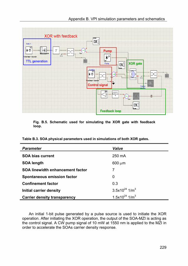
Appendix B. VPI simulation parameters and schematics
229
TTL generationXOR gate
Control signal
Pump
Feedback loop
TTL generationXOR gate
Control signal
Pump
Feedback loop
Fig. B.5. Schematic used for simulating the XOR gate with feedback loop.
Table B.3. SOA physical parameters used in simulations of both XOR gates.
Parameter Value
SOA bias current 250 mA
SOA length 600 m
SOA linewidth enhancement factor 7
Spontaneous emission factor 0
Confinement factor 0.3
Initial carrier density 3.5x1024 1/m3
Carrier density transparency 1.5x1024 1/m3
An initial 1-bit pulse generated by a pulse source is used to initiate the XOR operation. After initiating the XOR operation, the output of the SOA-MZI is acting as the control signal. A CW pump signal of 10 mW at 1550 nm is applied to the MZI in order to accelerate the SOAs carrier density response.

Appendix B. VPI simulation parameters and schematics
230
Following the 1-bit binary subtraction algorithm explained in Chapter 6, the first XOR gate provides the ‘1’ bits needed for the following conjugation operation. This XOR gate output acts as one of the inputs of the second XOR gate. The other input is the TTL generated in the simulation scheme shown in Fig. B.5. Fig. B.6 illustrates the simulated scheme for the second XOR gate. The output of the first XOR gate is attenuated (Att = 2.2 dB) and synchronized with the TTL input (optical delay = 90 ps). The SOAs parameters are the same as the previous case (Table B.3). The control signal is a Gaussian pulsed source at 1558 nm with a peak power of 2 mW. A CW pump signal at 1550 nm is also applied to the MZI. Finally, the output of the second XOR is filtered with a 1-nm optical filter.
TTL input
XOR 1 output
XOR gateControl signal
Pump
TTL input
XOR 1 output
XOR gateControl signal
Pump
Fig. B.6. Schematic used for simulating the second XOR gate.
The simulation results of the whole architecture have been shown in Chapter 6.

231
Appendix C
List of Ph.D. publications
The following is a list of publications, and conference proceedings authored by Ruth Vilar Mateo arising from her PhD research.
[1] R. Vilar, F. Ramos, and J. Marti, “Tecnicas de deteccion de fallo y monitorizacion de la señal en tiempo real en redes de conmutacion de paquetes,” in Proc.of Jornadas Telecom I+D, Madrid (Spain), 2006.
[2] R. van Caenegem, D. Roccato, and R. Vilar, “Evolution towards an all-optically switched packet network: the LASAGNE viewpoint,” in Proc. of 11th European Conference on Networks & Optical Communications (NOC’06), Berlin (Germany), 2006.
[3] R. Vilar, F. Ramos, and J. Marti, “Optical signal quality monitoring in packet-switched networks through optical pulse correlation,” in Proc. of 12th European Conference on Networks & Optical Communications (NOC’07), Stockholm (Sweden), 2007.

Appendix C. List of Ph.D. publications
232
[4] R. Vilar, F. Ramos, and J. Marti, “Optical signal quality monitoring using fibre-Bragg-grating-based correlators in optical packet-switched networks”, in Proc of. 33rd European Conference on Opical Communications (ECOC’07), Berlin (Germany), 2007.
[5] R. Van Caenegem, D. Colle, M. Pickavet, P. Demeester, K. Christodoulopoulos, K. Vlachos, E. Varvarigos, D. Roccato, and R. Vilar, “The design of an all-optical packet switching network,” IEEE Communications Magazine, vol. 45, pp. 52-61, 2007.
[6] R. Vilar, J.M. Martinez, F. Ramos, and J. Marti, “All-optical decrementing of a packet’s time-to-live (TTL) field using logic XOR gates,” in Proc. of 6th International Symposion Communication Systems, Networks and Digital signal processing (CSNDSP’08), Graz (Austria), 2008.
[7] R. Vilar, J.M. Martinez, F. Ramos, and J. Marti, “All-optical DGD monitor for packet-switched networks based on an integrated active Mach-Zehnder interferometer operating as logic XOR gate,” Optics Communications, vol. 281, pp. 5330-5334, 2008.
[8] R. Vilar, J.M. Martinez, F. Ramos, and J. Marti, “All-optical decrementing of a packet’s time-to-live (TTL) field using logic XOR gates,” Optics Express, vol. 16, no. 24, pp. 19734-19740, 2008.
[9] R. Vilar, J. Garcia, G. Tremblay, Y. Kim, S. Larochelle, F. Ramos, and J. Marti, “OSNR monitoring at high-speeds using a FBG-based correlator in optical packet-switched networks,” in Proc. Optical Fiber Communication Conference (OFC’09), San Diego (CA, USA), 2009.
[10] R. Vilar, J. Garcia, Y. Kim, S. Larochelle, and F. Ramos, “Path Monitoring for Restoration Functions in Optical Packet-Switched Networks,” in Proc.of International Conference on Transparent Optical Networks (ICTON’09), Azores (Portugal), 2009.
[11] R. Vilar, J.Garcia, G. Tremblay, Y. Kim, S. LaRochelle, F. Ramos and J. Marti, “Monitoring the Quality of Signal in Packet-Switched Networks Using Optical Correlators,” IEEE/OSA J. Lightwave Technol., vol. 27, no. 23, pp. 5417-5425, 2009.

Appendix C. List of Ph.D. publications
233
[12] R. Vilar, R. Llorente, and F. Ramos, “Monitoring devices for OSNR-assisted routing in optical packet-switced networks,” in Proc. of Future Network & Mobile Summit, Florence (Italy), 2010.
[13] R. Vilar, N. Nadarajah, A. Nirmalathas, R. Llorente, and F. Ramos, “A CD and OSNR-insensitive DGD monitoring technique for high-speed data using a low-speed detector,” in Proc.of Acces Networks and In-house Communications (ANIC’10), Karlsruhe (Germany), 2010.
[14] R. Vilar, N. Nadarajah, A. Nirmalathas, R. Llorente, and F. Ramos, “Low-cost PMD monitoring technique for high-speed data,” submitted to Optics Express in 2010.