onboard processing satellite network architecture and ... · onboard processing satellite network...
TRANSCRIPT
Contractor Report Number: CRI 8081 7
ONBOARD PROCESSING
SATELLITE NETWORK ARCHITECTURE
AND
CONTROL STUDY
FINAL REPORT
NASA CONTRACT NAS3-24886
JUNE 1987
PREPARED BY
S. JOSEPH CAMPANELLA
BENJAMIN A. PONTANO
AND
HARVEY CHALMERS
COMSAT LABORATORIES
CLARKSBURG, MARYLAND
https://ntrs.nasa.gov/search.jsp?R=19870018278 2018-06-24T09:31:29+00:00Z
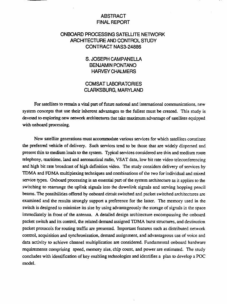
ABSTRACT
FINAL REPORT
ONBOARD PROCESSING SATELLITE NETWORK
ARCHITECTURE AND CONTROL STUDY
CONTRACT NAS3-24886
S. JOSEPH CAMPANELLA
BENJAMIN PONTANO
HARVEY CHALMERS
COMSAT LABORATORIES
CLARKSBURG, MARYLAND
For satellites to remain a vital part of future national and international communications, new
system concepts that use their inherent advantages to the fullest must be created. This study is
devoted to exploring new network architectures that take maximum advantage of satellites equipped
with onboard processing.
New satellite generations must accommodate various services for which satellites constitute
the preferred vehicle of delivery. Such services tend to be those that are widely dispersed and
present thin to medium loads to the system. Typical services considered are thin and medium route
telephony, maritime, land and aeronautical radio, VSAT data, low bit rate video teleconferencing
and high bit rate broadcast of high definition video. The study considers delivery of services by
TDMA and FDMA multiplexing techniques and combinations of the two for individual and mixed
service types. Onboard processing is an essential part of the system architecture as it applies to the
switching to rearrange the uplink signals into the downlink signals and serving hopping pencil
beams. The possibilities offered by onboard circuit switched and packet switched architectures are
examined and the results strongly support a preference for the latter. The memory used in the
switch is designed to minimize its size by using advantageously the storage of signals in the space
immediately in front of the antenna. A detailed design architecture encompassing the onboard
packet switch and its control, the related demand assigned TDMA burst structures, and destination
packet protocols for routing waffle are presented. Important features such as distributed network
control, acquisition and synchronization, demand assignment, and advantageous use of voice and
data activity to achieve channel multiplication are considered. Fundamental onboard hardware
requirements comprising speed, memory size, chip count, and power are estimated. The study
concludes with identification of key enabling technologies and identifies a plan to develop a POC
model.
NAS3-24886 FINAL REPORT
ONBOARD PROCESSING NETWORK
ARCHITECTURE AND CONTROL STUDY
FINAL REPORT
TABLE OF CONTENTS
1. Introduction
1.1 Networks and Services
1.2
,
1.1.1
1.1.2
1.1.3
Spot Beam Considerations
Demand Assigned, Multiple Access Networks
Intersatellite Links
1.1.4 Summary Of Objectives
Summary of Contract Tasks
1.2.1 Task 1 - Network Architecture
1.2.2 Task 2 - Network Control
1.2.3 Task 3 - Technology Challenges
Network Architectures
2.1 Services Carried
2.2
2.1.1 Identification Of Services
2.1.2 Categories Of Services
Future Communications Satellite Payloads
2.2.1 International Services And Extrapolations
2.2.2 Domestic Services And Extrapolations
1.1
1.1
1.1
1.2
1.3
1.3
1.3
1.3
1.5
1.6
2.1
2.1
2.1
2.2
2.4
2.5
2.6
PAGE 1
NAS3-24886 FINAL REPORT
2.3 Network Options
2.3.1 Simple Global Beam Networks
2.3.2 Regional Beam Networks
2.3.3 Spot Beam Networks
2.3.3.1 Spot Beam Advantages
2.3.3.2 Spot Beam Connectivity
2.3.3.3 Hopping Spot Beams
2.3.4 Onboard Switching And Storage
2.3.4.1 Operating Without Onboard Storage
2.3.4.2 Operating With Onboard Storage
2.3.4.3 Comparing Operation Without And With
Onboard Storage
2.3.4.4 Examples Of Operating Without And With
Onboard Storage
2.3.5 Intersatellite Links
2.4 Transmission Configurations
2.4.1 FDMA
2.4.2 TDMA
2.4.3 MF/TDMA
2.4.4 CDMA
2.4.5
2.4.5.1
Transmission Configurations
FDMA-FDMA Operation
PAGE 2
2.7
2.7
2.8
2.9
2.9
2.9
2.10
2.10
2.10
2.11
2.11
2.12
2.15
2.16
2.16
2.16
2.17
2.18
2.19
2.19
NAS3-24886
2.5
2.6
2.4.5.2
2.4.5.3
2.4.5.4
2.4.5.5
2.4.5.6
FINAL REPORT
FDMA-TDM/TDMA Operation
TDMA-TDMA Operation
TDMA-TDM/TDMA Operation
MF/TDMA-TDM/TDMA Operation
M F/TDMA-M F/TDMA Operation
Computer And Data Communications
2.5.1 Packet Communications On ACTS
2.5.1.1
2.5.1.2
2.5.1.3
Circuit Switched Operation
Stationary Preassigned Channel Operation
Future Onboard Packet Node
2.5.2 Configurations For Computer And DataCommunications
2.5.2.1
2.5.2.2
2.5.2.3
Circuit Switched Operation
Random Access With Preassigned Circuits
Onboard Packet Node Data Transmission
2.5.2.4 Comparison Of The Data Communications
Techniques
Advanced Satellite Telecommunications Options
2.6.1 Advanced Network Control
2.6.1.1
2.6.1.2
2.6.2
Call Processing On Board The Satellite
Destination Directed Onboard Switching
Memory In Space
PAGE 3
2.22
2.23
2.24
2.24
2.25
2.26
2.26
2.26
2.27
2.28
2.29
2.29
2.31
2.32
2.33
2.38
2.38
2.38
2.39
2.40
NAS3-24886 FINAL REPORT
2.6.3 Integrating In Other Services
2.6.3.1 Capability To Accommodate Different Services
2.6.3.2 Synchronization Among Different Services
2.6.3.3 Source Coding Considerations
Destination Directed Packet Onboard Processing
Architecture
System Design
=
3.1
3.1.1
3.1.1.1
3.1.2
3.1.2.1
3.1.2.2
3.1.2.3
3.1.2.4
3.1.2.5
3.1.2.6
3.1.2.7
3.1.3
3.1.4
3.1.5
3.1.5.1
3.1.5.2
Demand Assignment of Capacity
Destination Addresses Packet Message
Method of Operation
Call Set-Up Procedure
Call In Progress Procedure
Call Termination
Mapping Functions
Detailed Call Set-Up Procedure
Detailed Call In Progress Procedure
Detailed Call Termination Procedure
Packet Frame Efficiency
Digital Speech Interpolation
Acquisition and Synchronization Control
Reference Bursts
Uplink Request Bursts
PAGE 4
2.41
2.41
2.41
2.42
3.1
3.1
3.1
3.2
3.3
3.3
3.4
3.5
3.5
3.6
3.6
3.9
3.9
3.10
3.10
3.11
3.12
NAS3-24886
3.1.5.3
3.1.6
3.1.7
3.1.7.1
3.1.7.2
FINAL REPORT
Acquisition and Synchronization Procedure
Overall Frame Efficiency
Onboard Switch Architectures
Separate Input/Output Memory Architecture
Unified Memory Architecture
3.2 Baseband Processing Implementation
3.2.1
3.2.1.1
3.2.1.1.1
3.2.1.1.1.1
3.2.1.1 ol .2
3.2.1.1.1.3
3.2.1.1.1.4
3.2.1.1.2
3.2.1.1.2.1
3.2.1.1.2.2
3.2.1.2
3.2.2
3.2.2.1
3.2.2.1.1
Separate Input/Output Memory Architecture
Separate Input/Output Memory Hardware
Implementation
System Memory Requirements
Input/Output Memory Requirements
Control Memory Requirements
Switch State Memory Requirements
Packet Header Memory and Control
Separate Memory System Block Diagram
Input Subsystem Block Diagram
Output Subsystem Block Diagram
Conclusions - Separate Memory Architecture
Unified Memory Architecture
Unified Memory Hardware Implementation
System Memory Requirements
3.12
3.13
3.15
3.15
3.16
3.19
3.19
3.21
3.22
3.23
3.24
3.25
3.26
3.27
3.28
3.29
3.31
3.32
3.35
3.35
PAGE 5
NAS3-24886
3.2.2.1.1.1
3.2.2.1.1.2
3.2.2.1.2
3.2.2.1.3
.
4.1
4.2
FINAL REPORT
Unified Data Memory Requirements
Unified Header Memory Requirements
Unified Memory System Block Diagram
Unified Memory Control Subsystem
Block Diagram
3.2.2.2 Conclusions - Unified Memory Architecture
3.2.3 Alternative Unified Memory Architecture
3.2.3.1 Alternative Unified Memory Hardware
' Implementation
3.2.3.1.1 System Memory Requirements
3.2.3.1.2 Alternative Unified Memory Hardware
Block Diagram
3.2.3.1.2.1 Alternative Unified Memory Serial Input
Mux Block Diagram
3.2.3.1.2.2 Alternative Unified Memory Serial Output
Mux Block Diagram
3.2.3.2 Conclusions - Alternative Unified Memory
Integration Of Other Services
Mobile Satellite Service
4.1.1 Integrated Fixed Satellite and Land Mobile
Satellite Services
4.1.2 System Characteristics
Call Set-Up Procedures
4.2.1 Calls Originating at MT to BS or Gateway
3.36
3.36
3.37
3.39
3.39
3.40
3.41
3.43
3.44
3.45
3.45
3.48
4.1
4.1
4.1
4.2
4.3
4.3
PAGE 6
NAS3-24886 FINAL REPORT
4.2.2 Calls Originating at BS or Gateway to MT
4.2.3 Calls Originating at a MT Destined to a MT
4.3 Impact on the OnBoard Packet Processor
4.3.1 Integration Of FSS and MSS
4.3.2 MSS Implementation
4.3.3 Difference In Traffic Bit Rates Of MSS/FSS
Links
4.4 Intersatellite Link Operation
5. Technology Forecast For Static Ram and
Custom Development
5.1 Technology Forecast For Static Rams
5.2 Technology Forecast For Custom and Semi-Custom
Logic Arrays
6.0 Technology Development Requirements
6.1 Key Device Development
6.1.1 Custom Logic Devices
6.1.2 Memory Development
6.2 Destination Directed Packet Onboard Processing
Architecture Development
6.3 Destination Directed Packet Network Control Test Bed
6.3.1 Critical Features To Be Investigated
6.3.2 Proposed POC Test Bed Breadboard
7. References
4.4
4.4
4.5
4.5
4.5
4.6
4.7
5.1
5.2
5.4
6.1
6.1
6.2
6.2
6.2
6.3
6.3
6.3
7.1
PAGE 7
NAS3-24886 FINAL REPORT
A.1
A.2
Appendices
Onboard Baseband Switch Call Processing
Number of Possible Switch States for MxN Switch
A1.1
A2.1
PAGE 8
NAS3-24886 FINAL REPORT
LIST OF FIGURES
Figure 1.1
Figure 1.2
Figure 2.1
Figure 2.2
Figure 2.3
Figure 2.4
Figure 2.5
Figure 2.6
Figure 2.7
Figure 2.8
Figure 2.9
Figure 2.10
Figure 2.11
Figure 3.1
Figure 3.2
Multi-Service Switching and Routing
Satellite Gateway
Extended World Coverage With Inter-Satellite Link
Intelsat V Beam Connections
Intelsat Vl Beam Connections
Intelsat Vl Beam Connections Using6X6 MS
6X6 MSM Switch State Time Plan
Spot Beam Antenna Coverage of AtlanticOcean Basin Countries
Preassigned Routes for Random AccessTDMA
Single Down Beam Dwell
Preassigned Routes in Superframe For
Random Access
Circuit Switching Data Transmission
Random Access Data Transmission with
Preassigned Channels
On-Board Packet Node Data
Transmission
TDMA/DAMA System with Onboard Processor
Uplink Capacity Reallocation
1.7
1.8
2.44
2.45
2.46
2.47
2.48
2.49
2.50
2.51
2.52
2.54
2.55
3.50
3.51
PAGE 9
NAS3-24886 FINAL REPORT
Figure 3.3
Figure 3.4
Figure 3.5
Rgure 3.6
Figure 3.7
Figure 3.8
Figure 3.9
Figure 3.10
Figure 3.11
Figure 3.12
Figure 3.13
Figure 3.14
Figure 3.15
Figure 3.16
Figure 3.17
Figure 3.18
Figure 3.19
Onboard Satellite Channel Mapping
Terrestrial Port to Time Slot Mappingand Up-Link to Down-Link Satellite
Channel Mapping For Destination
Directed Message Switching
Destination Directed Packet System
Mapping
Packet Header Structure
Traffic Bursts for Packet Routing
Traffic Bursts for Sub-burst Routing
Packet Header Efficiency for Individual Packet
Routing
Packet Header Efficiency for Sub-Burst Packet
Routing
Frame Format
Superframe Structure
Reference Burst Format
Request Burst (RQB) Structure
Relationship Between Beam Dwell andSub-Burst
Separate Input/Output Memory Architecture
Unified Pingpong Memory Architecture
Unified Dual Port Memory Architecture
Onboard Dual Port Switch Operation
3.52
3.53
3.54
3.55
3.56
3.57
3.58
3.59
3.60
3.61
3.62
3.63
3.64
3.65
3.66
3.67
3.68
PAGE 1 0
NAS3-24886 FINAL REPORT
Figure 3.20 Signal Flow for Separate Memory Architecture
Destination-Directed SwitchingBetween Beams
3.69
Figure 3.21 Control Memory Maps and Pointers for Separate
Memory Architecture of Figure 3.20
3.70
Figure 3.22 Separate Memory Architecture Hardware
Block Diagram
3.71
Figure 3.23 Detailed Hardware Block Diagram of
Input Section
3.72
Figure 3.24 Detailed Hardware Block Diagram of
Output Section
3.73
Figure 3.25 Signal Flow for Unified Memory Architecture
Destination-Directed Switching BetweenBeams
3.74
Figure 3.26 Scrambling Problem with 64-bit Bus 3.75
Figure 3.27 Diagram of Pointer Array to Solve
Scrambling Problem
3.76
Figure 3.28 Unified Memory Architecture Hardware
Block Diagram
3.77
Figure 3.29 Detailed Hardware Block Diagram of
Control Section Unified MemoryArchitecture
3.78
Figure 3.30 Alternative Signal Flow for Unified
Memory Architecture
3.79
Figure 3.31 Alternative Unified Memory Hardware
Block Diagram
3.80
Figure 3.32 Block Diagram of Serial Input Mux 3.81
PAGE 1 1
NAS3-24886 FINAL REPORT
Figure 3.33 Block Diagram of Serial Output Demux 3.82
Figure 4.1 Network Elements of An Integrated
FSS and MSS Satellite System
4.9
Figure 4.2 MSS Frequency Plans 4.10
Figure 4.3 Onboard Packet Processor For
Integrated FS & MS Services
4.11
Figure 4.4 MSS Processor 4.12
Figure 5.1 Speed-Power Products of Various Digital
IC Technologies {Source: N. Mokhoff,
Comouter Design, p 77, Oct. 15, 1985}
5.8
Figure 5.2 Forecast of Commercial GAAS Digital
Logic IC Gate Complexity vs. Commercial
Silicon IC's
5.9
Figure 5.3 GaAs Device Technology 5.10
Figure 6.1 Destination Directed Packet Switching
Test Bed Block Diagram
6.6
Figure 6.2 Test Bed Program Plan 6.7
PAGE 1 2
NAS3-24886 FINAL REPORT
LIST OF TABLES
Table 1.1 Objectives 1.4
Table 2.1 Satellite Services and Attributes 2.3
Table 2.2 Comparison of Beam Hopping Parameters
with and without Onboard Memory
2.12
Table 2.3 Example I of the Comparison of Beam
Hopping Parameters with and without
Onboard Memory
2.13
Table 2.4 Example 2 of the Comparison of Beam
Hopping Parameters with and without
Onboard Memory
2.14
Table 2.5 Example of the Comparison of Beam
Hopping Parameters With and Without
Onboard Memory
2.15
Table 2.6 Uplink and Downlink Transmission
Configurations
2.21
Table 2.7 Comparison of three Onboard Switch
Implementations
2.36
Table 3.1 System Operation for Destination
Addressed Message Packet System
3.3(A)
3.3(8)
Table 3.2 Call Set-Up Procedure 3.7
Table 3.3 Memory Requirements for Separate
Architecture, Total for 10 120 MBPS Beams
3.27
Table 3.4 Subsystem Device Count and Power
Dissipation
3.30
PAGE 1 3
NAS3-24886 FINAL REPORT
Table 3.5 Memory Requirements for Unified Memory
Architecture, Total for 10 120 MBPS Beams
3.36
Table 3.6 Subsystem Device Count and Power
Dissipation - Unified Memory Architecture
3.38
Table 3.7 Memory Requirements for Alternative
Unified Memory Architecture, Total for10 120 MBPS Beams
3.43
Table 3.8 Subsystem Device Count and Power
Dissipation - Alternative Unified Memory
Architecture (Based on 1987 Technology)
3.47
Table 5.1 Subsystem Device Count and Power
Dissipation - Alternative Unified
Memory Architecture (Based on 1990-1992
Technology
Table 5.2 SRAM Technology Rankings According
To McDonnell Douglas Study
5.3(A)
Table 5.3 Summary of Future Custom Chip
Requirements For Alternative Unified
Memory Architecture
5.5
PAGE 1 4
NAS3-24886 FINAL REPORTONBOARD PROCESSINGSATELLITE NETWORK
ARCHITECTUREANDCONTROL STUDYFINAL REPORT
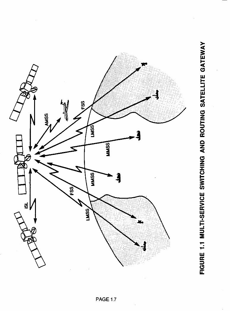
1. INTRODUCTION
Satellites, as a consequence of the natural forces of the market
place over more than two decades of application, have been applied to a
variety of services incorporating a variety of transmission means. Figure
1.1 illustrates the generic services delivered by satellite systems. These
include fixed satellite services (FSS), maritime mobile services (MMSS),
land mobile services (LMSS), aeronautical mobile satellite services
(AMSS) and intersatellite link (ISL). By far the greatest use lies in the
FSS area which supports domestic and international multiple trunk, SCPC
and DAMA SCPC telephone and data. Also FSS supports the broadcast
distribution of television for the major TV networks and for cable TV. The
mobile satellite services currently constitute a small fraction of the total
and this resides principally in the MMSS; however because of the changing
complexion of the satellite communication industry which will accentuate
the prime advantages of satellites (which are multiple access and demand
assignment of the space segment) and the expansion of AMSS and LMSS the
mobile fraction is expected to grow significantly. The ISL has been used
in the TDRSS and some military satellites but has not yet been used in a
commercial application. This is expected to change as regional gateway
switching satellites appear and interconnection of these gateways to
exchange traffic between regions occurs. Any new generation of
satellites should be capable of accommodating these services. It is
important to bear in mind that the competition from terrestrial
transmission media, in particular high capacity, low cost lightguides
operating at digital transmission rates per individual fiber potentially
approaching a Gigabit per second, are forcing satellite systems to adopt
technologies that lead to significantly reduced cost. Such cost reduction
must consider the balance of cost between the space segment and the
earth segment.
1.1 NETWORKS AND SERVICES
1.1.1 SPOT BEAM CONSIDERATIONS
The most economical satellite system results when the space
segment is enhanced to provide high e.i.r.p, and gain to noise temperature
(G/T) ratios and the earth segment uses this space segment to advantage
by using small, low power stations to deliver the service. This leads to a
PAGE 1.1
NAS3-24886 FINAL REPORT
space segment that has large aperture antennas and consequently narrow
spot beams. However, the narrow spot beams reduce the coverage area of
any one beam requiring either that many such spot beams be used
simultaneously or that a few beams hop to various regions and dwell in
each long enough to accommodate the traffic. The spot beams can be fixed
if the region they cover carries sufficient traffic to fill the beam. This is
suitable for regions that encompass areas of high population density.
However, in regions where the density is sparse the beam must hop about
to accumulate sufficient traffic to fill it. In the study reported here, this
type of system receives the principal attention. The system studied also
interconnects with a larger beam.
The services carried over satellites have evolved as a consequence of
a selection process that uses the inherent properties to greatest
advantage. In this regard, the most attractive property of the satellite is
its ability to view almost half the earth's surface from a single vantage
point 22300 miles above the equator. Any station in sight of the satellite
can communicate to any other station in sight of the same satellite no
matter where it is located. Satellites also provide large bandwidth any
portion of which, when desired, can be divided into narrow channels.
These capabilities have resulted in the world wide distribution of
broadcast quality TV and the distribution of demand assigned services for
individual telephone and data circuits by both FDMA single channel per
carrier techniques and by TDMA techniques for both national (domestic)and international services.
1.1.2 DEMAND ASSIGNED, MULTIPLE ACCESS NETWORKS
Demand assigned multiple access use of satellites which permits
space segment capacity to be used when needed and returned for use by
another when not needed by any user in view of the satellite constitutes
the most powerful communications networking concept known. This
property is most valuable for thin route users each of whom uses only a
small fraction of an Erlang, but it remains useful for traffic intensities of
several Erlangs between destinations. For example, a network of 1000
stations, each serving a traffic intensity averaging 0.2 erlangs can be
accommodated with only 250 space segment circuits. The power of
demand assignment diminishes on routes bearing traffic intensities
greater than 20 Erlangs between destinations. Thus, high intensity routes
such as those carrying telephone traffic between the major industrial
countries of the North Atlantic Region do not enjoy the DAMA advantage.
However on such routes, another advantage, namely that of distributed
origins and destinations in which the traffic can be initiated near or at its
PAGE 1.2
NAS3-24886 FINAL REPORT
origin and delivered near or at its destination thus minimizing use of or
bypassing all together terrestrial links, is realized. This latter satellite
advantage will become very significant in the competitive race between
cables and satellites in the international and national arenas provided the
cost of satellite earth stations can be very significantly reduced by
introduction of a proper space segment that also has reasonable cost.
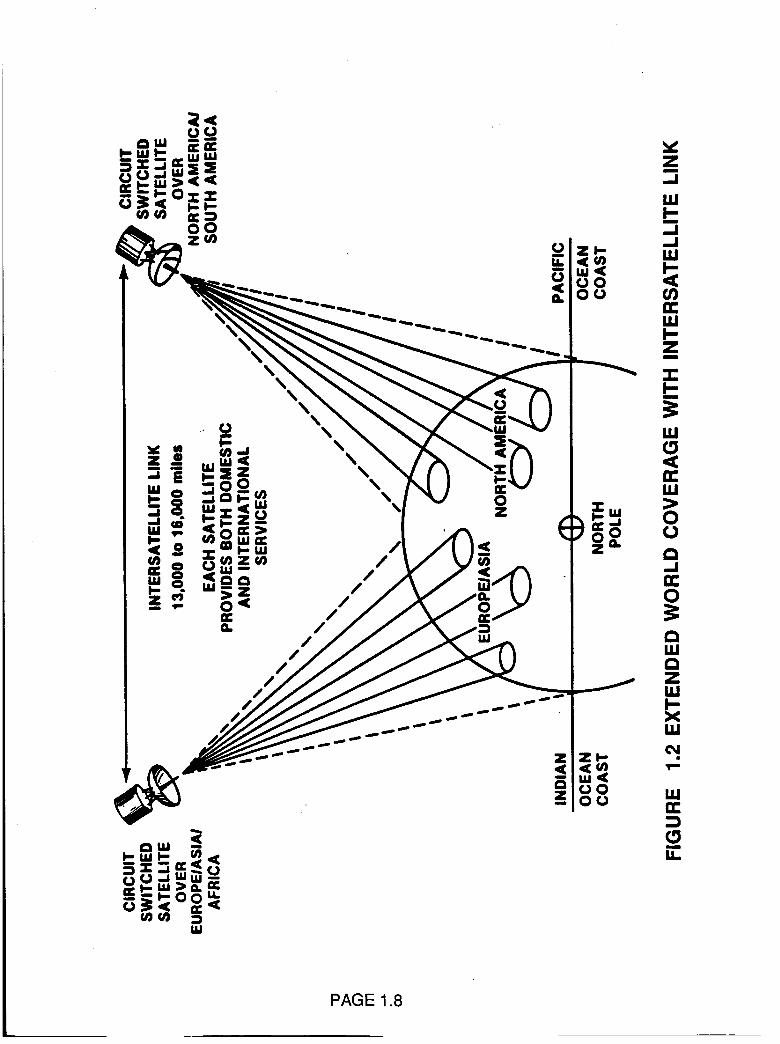
1.1.3 INTERSATELLITE LINKS.
Intersatellite links provide direct connections between satellites. A
question frequently asked is "what use can be made of the intersatellite in
commercial satellite applications?" One answer is to bridge between two
satellites one located over the North/South America continents and the
other over Europe/Middle East/Africa continents to provide a combination
of domestic and international traffic. If these satellites are positioned
approximately 57 ° apart (i.e. 13000 miles apart)in the geostationary orbit
as illustrated in Figure 1.2 then individually each can serve domestic andNorth/South international traffic for the continents beneath it and the
intersatellite link can provide East/West international connections. The
added one way propagation delay time is 72 ms which will extend the
round trip propagation time from the present nominal value of 550 ms to
694 ms. This is a small increase that should not greatly change
conversational user subjective reaction. Also the impact on data should be
unchanged compared to that experienced on the nominal single hop delaypath.
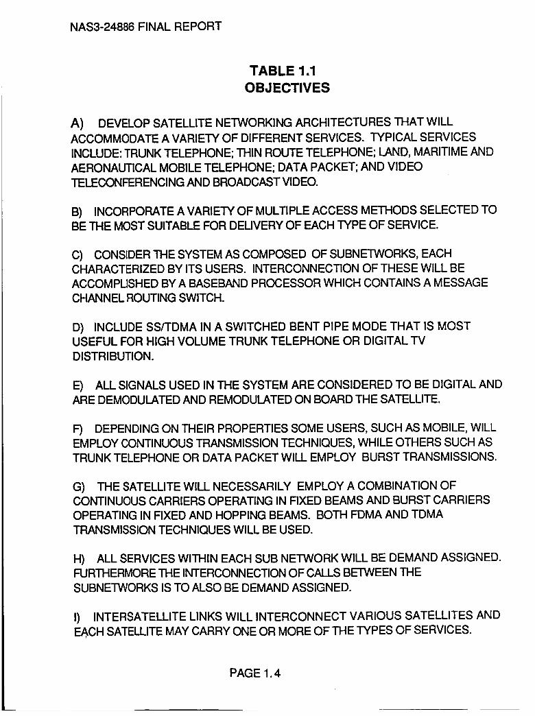
1.1.4 SUMMARY OF OBJECTIVES
The satellite system of the future must fulfill the objectives set
forth in Table 1.1 to make the most effective use of its inherent
advantages and be competitive in the new market place.
1.2 SUMMARY OF CONTRACT TASKS
The work under the contract is divided into three tasks:
1.2.1 TASK 1 - NETWORK ARCHITECTURE
Segment the market for telecommunications services into user
classes having similar transmission requirements and hence similarnetwork architectures.
PAGE 1.3
NAS3-24886 FINAL REPORT
TABLE 1.1OBJECTIVES
A) DEVELOP SATELLITE NETWORKING ARCHITECTURES THAT WILL
ACCOMMODATE A VARIETY OF DIFFERENT SERVICES. TYPICAL SERVICES
INCLUDE: TRUNK TELEPHONE; THIN ROUTE TELEPHONE; LAND, MARITIME AND
AERONAUTICAL MOBILE TELEPHONE; DATA PACKET; AND VIDEO
TELECONFERENCING AND BROADCAST VIDEO.
B) INCORPORATE A VARIETY OF MULTIPLE ACCESS METHODS SELECTED TOBE THE MOST SUITABLE FOR DELIVERY OF EACH TYPE OF SERVICE.
C) CONSIDER THE SYSTEM AS COMPOSED OF SUBNETWORKS, EACHCHARACTERIZED BY ITS USERS. INTERCONNECTION OF THESE WILL BE
ACCOMPLISHED BY A BASEBAND PROCESSOR WHICH CONTAINS A MESSAGE
CHANNEL ROUTING SWITCH.
D) INCLUDE SS/TDMA IN A SWITCHED BENT PIPE MODE THAT IS MOSTUSEFUL FOR HIGH VOLUME TRUNK TELEPHONE OR DIGITAL TV
DISTRIBUTION.
E) ALL SIGNALS USED IN THE SYSTEM ARE CONSIDERED TO BE DIGITAL ANDARE DEMODULATED AND REMODULATED ON BOARD THE SATELLITE.
F) DEPENDING ON THEIR PROPERTIES SOME USERS, SUCH AS MOBILE, WILL
EMPLOY CONTINUOUS TRANSMISSION TECHNIQUES, WHILE OTHERS SUCH AS
TRUNK TELEPHONE OR DATA PACKET WILL EMPLOY BURST TRANSMISSIONS.
G) THE SATELLITE WILL NECESSARILY EMPLOY A COMBINATION OFCONTINUOUS CARRIERS OPERATING IN FIXED BEAMS AND BURST CARRIERS
OPERATING IN FIXED AND HOPPING BEAMS. BOTH FDMA AND TDMA
TRANSMISSION TECHNIQUES WILL BE USED.
H) ALL SERVICES WITHIN EACH SUB NETWORK WILL BE DEMAND ASSIGNED.FURTHERMORE THE INTERCONNECTION OF CALLS BETWEEN THE
SUBNETWORKS IS TO ALSO BE DEMAND ASSIGNED.
I) INTERSATELLITE LINKS WILL INTERCONNECT VARIOUS SATELLITES AND
EACH SATELLITE MAY CARRY ONE OR MORE OF THE TYPES OF SERVICES.
PAGE 1.4
NAS3-24886 FINAL REPORT
A) Consider use of the following transmission architectures:
• Satellite switched TDMA
• TDMA up, TDM down
• Scanning ( hopping ) beam TDMA
• FDMA up, TDM down
• Satellite Switched MF/TDMA
• Switching Hub earth stations with double hop transmission.
B) Select a candidate network architecture that:
• Comprises multiple access subnetworks optimized for each user.
• Interconnects the subnetworks by means of a baseband
processor.
• Optimizes the marriage of interconnection and access techniques.
1.2.2 TASK 2 - NETWORK CONTROL
Provide an overall network control architecture that will serve the
needs of the baseband and satellite switched RF interconnected
subnetworks. This architecture shall consider the provision of the
following network control functions:
• Intelligent Onboard Baseband Processor
• Distributed Network Control
• Acquisition and Synchronization
• Demand Assignment
• Fade Compensation
• Traffic and BBP Scheduling Procedures
PAGE 1.5
NAS3-24886 FINAL REPORT
• Network Timing and Synchronization
• Onboard Clock Control
1.2.3 TASK 3. - TECHNOLOGY CHALLENGES
The results of the studies shall be used to identify elements of
network architecture and control that require the greatest degree of
technology development to realize an operational system. This will be
specified in terms of :
• Requirements of the Enabling Technology.
• Difference From the Current Available Technology.
• Estimate of the Development Requirements Needed to Achieve An
Operational System
The results obtained for each of these tasks are presented sections
2, 3, and 4 of this report.
PAGE 1.6
W
Zm
0_C
C_Z
Z
m
mI
m
=E
V"
m_c
u.
PAGE 1,7
LU
ZU.Il--Xmmm
I.LI
m
IL
PAGE 1.8
NAS3-24886 FINAL REPORT
2 NETWORK ARCHITECTURES
2.1 SERVICES CARRIED
2.1.1 IDENTIFICATION OF SERVICES
Various classes of telecommunications services can be expected to be
supported by an advanced satellite communications system. These may be
integrated into a common network on a single satellite or they may be
carried as separate networks over different satellites individually
designed to optimize each type of service.
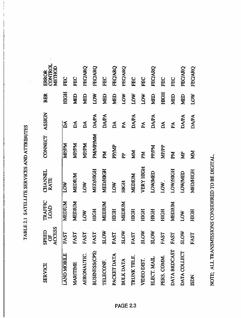
Table 2.1 lists various telecommunications services that are
expected to be carried on the satellites of the late 20th and early 21st
century. Transmission attributes are identified for each service type inthis table. The attributes and their definitions are listed below:
Speed Of Access Refers to the speed with which the service must
be established following the instant of a request.
FAST refers to response in tens of seconds andSLOW in minutes to hours.
Traffic Load Refers to traffic intensity on the channels
provided. LOW refers to fractions of Erlangs,
MEDIUM to 1 to 20 Erlangs and HIGH to >20 Erlangs.
Channel Rate Refers to the bit rate on the channel carrying the
service. LOW refers to rates less than 16 kbit/s,
MEDIUM to rates between 16 Kbit/s and 20 Mbit/s,
HIGH to rates between 20 and 140 Mbit/s and VERY
HIGH to rates > 140 Mbit/s.
Connectivity PP is point-to-point, MP is multipoint-to-point,
PM is point-to-multipoint and MM is
multipoint-to-multipoint or full mesh.
Assignment Refers to either PA for preassigned or DA for
demand assigned.
BER Refers to the bit error rate on the transmission
that can be tolerated to carry the service. LOW is
<10 -8 , MEDIUM is <10 -6 and HIGH is <10 -3
PAGE 2. 1
NAS3-24886 FINAL REPORT
Error Control
Method
Refers to use of either Forward Error Correction
(FEC) or Automatic Repeat Request (ARQ)
2.1.2 CATEGORIES OF SERVICES
The various services can be organized into the following four
categories that are based on discipline rather than attributes:
1. MOBILE COMMUNICATIONS
Land
Maritime
Aeronautical
Personal
2. COMPUTER AND DATA COMMUNICATIONS
Packet Data
Bulk File Transfer
Data Collection
Data Broadcast
3. TELECOMMUNICATIONS
Trunk TelephoneISDN
Business (Customer Premises Station)
Teleconference
Electronic Mail
4. BROADCAST VIDEO
Network Video Distribution
Cable Video Distribution
Educational Video Distribution
The mobile group is characterized by fast access speed, low to
medium traffic load per terminal, predominantly low channel transmission
rate, mostly multipoint to point and point to multipoint connectivities,
medium to high BER and strong dependence on FEC to overcome the vagaries
of the transmission links.
PAGE 2. 2
PAGE 2.3
NAS3-24886 FINAL REPORT
The computer and data group has mixed characteristics. Access speed
should be fast for packet and broadcast data but slow for bulk
transmission and data collection. Channel transmission rate is high for
bulk transmission, medium for broadcast and packet and low for data
collection. Connectivity is point to point for bulk data, multipoint to point
and point to point for packet data, point to multipoint for broadcast data
and multipoint to point for data collection.
The telecommunications group also has mixed characteristics.
Access speed is fast for trunk telephone, ISDN and business CPS telephone
but slow for video teleconferencing and electronic mail. Traffic load is
high for trunk telephone, ISDN, business CPS telephone and electronic mail
(assuming concentration of traffic) and medium for teleconferencing.
Channel rate is medium to high for all but the electronic mail which
ranges from low to medium. Connectivity is full mesh, point to multipoint
and point to point. Assignment is preassigned and demand assigned for all
members in this group. BER is low for all except electronic mail which
may be medium or high when ARQ is used. FEC is used for all of these
services to meet the high quality standards that have come to be expected
for telecommunications with the possible exception of electronic mail
when protected by ARQ.
The broadcast video group comprise services that today are
exclusively carried by analog means. However in the future, because of the
research being performed in the laboratories on video source coding, it can
be expected that digital transmission at rates as low as 20 Mbit/s for
broadcast quality video equivalent to today's NTSC/PAL/SECAM quality and
80 Mbit/s for high definition 1050/1125 line broadcast video can be
expected. The transmission of these signals over satellite links requires
slow access, high traffic loads, high channel rates, point to multipoint
preassigned connectivity, low BER and application of FEC.
2.2 FUTURE COMMUNICATION SATELLITE PAYLOADS
Future satellite communications payloads will support all or some
subset of the services identified above. A good place to begin is to review
some of the types of payloads currently in use or anticipated and project
their logical extrapolations. Todays international satellites are designed
to support principally the telecommunications and video broadcast groups
with the recent addition of the maritime mobile service. It can be
expected that the mobile services will include aeronautical in the early1990s.
PAGE 2. 4
NAS3-24886 FINAL REPORT
2.2.1 International Services and Extrapolations
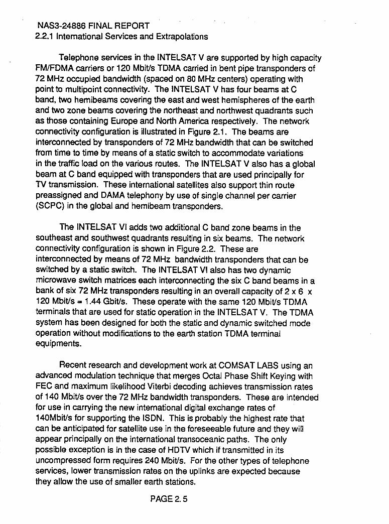
Telephone services in the INTELSAT V are supported by high capacity
FM/FDMA carriers or 120 Mbit/s TDMA carried in bent pipe transponders of
72 MHz occupied bandwidth (spaced on 80 MHz centers) operating with
point to multipoint connectivity. The INTELSAT V has four beams at C
band, two hemibeams covering the east and west hemispheres of the earth
and two zone beams covering the northeast and northwest quadrants such
as those containing Europe and North America respectively. The network
connectivity configuration is illustrated in Figure 2.1. The beams are
interconnected by transponders of 72 MHz bandwidth that can be switched
from time to time by means of a static switch to accommodate variations
in the traffic load on the various routes. The INTELSAT V also has a global
beam at C band equipped with transponders that are used principally for
TV transmission. These international satellites also support thin route
preassigned and DAMA telephony by use of single channel per carrier
(SCPC) in the global and hemibeam transponders.
The INTELSAT Vl adds two additional C band zone beams in the
southeast and southwest quadrants resulting in six beams. The network
connectivity configuration is shown in Figure 2.2. These are
interconnected by means of 72 MHz bandwidth transponders that can be
switched by a static switch. The INTELSAT Vl also has two dynamic
microwave switch matrices each interconnecting the six C band beams in a
bank of six 72 MHz transponders resulting in an overall capacity of 2 x 6 x
120 Mbit/s = 1.44 Gbit/s. These operate with the same 120 Mbit/s TDMA
terminals that are used for static operation in the INTELSAT V. The TDMA
system has been designed for both the static and dynamic switched mode
operation without modifications to the earth station TDMA terminal
equipments.
Recent research and development work at COMSAT LABS using an
advanced modulation technique that merges Octal Phase Shift Keying with
FEC and maximum likelihood Viterbi decoding achieves transmission rates
of 140 Mbit/s over the 72 MHz bandwidth transponders. These are intended
for use in carrying the new international digital exchange rates of
140Mbit/s for supporting the ISDN. This is probably the highest rate that
can be anticipated for satellite use in the foreseeable future and they will
appear principally on the international transoceanic paths. The only
possible exception is in the case of HDTV which if transmitted in its
uncompressed form requires 240 Mbit/s. For the other types of telephone
services, lower transmission rates on the uplinks are expected because
they allow the use of smaller earth stations.
PAGE 2. 5
NAS3-24886 FINAL REPORT
Both the INTELSAT V and Vl are also equipped with fixed spot beams
at Ku band pointed at North America and Europe respectively in the
Atlantic Ocean Region to serve the international business services (IBS)
and intermediate data rate (IDR) services which operate using terminals
with antennas of 3.5 to 7.5 m diameter equipped with HPAs of several
hundred watts. The IBS services are used by corporations to establish
private, open architecture international business communications
networks. The IDR services are used by telephone companies and PTTs to
carry international PSTN ( Public Switched Telephone Network) services.
The high EIRP (45 to 48 dBw) and G/T (0 to 3 dB/K) of the Ku band spot
beams makes it possible to operate with small low power earth stations.
This has created a high demand for use of the INTELSAT Ku band
transponders.
2.2.2 Domestic Services and Extrapolations
In the U.S. domestic arena, Ku band satellites with CONUS beams are
used extensively for multipoint to point VSAT data services, full mesh
DAMA SCPC telephony and point to multipoint preassigned telephony at T1
primary multiplex rates using FDMA and TDMA carriers in transponders
having 36 MHz bandwidth (spaced on 40 MHz centers) at C band and 44 MHz
bandwidth (spaced on 49 MHz centers) at Ku band. T1 rates (1.544 Mbit/s)
are used for telephone and teleconferencing. Small antenna terminal
operation at C-band is frequently impeded because of interference with
terrestrial and other satellite services making Ku band operation more
attractive. Typical U.S.domestic satellites include SATCOM, WESTAR,
TELSTAR, GALAXY and COMSTAR at C-band, SBS at Ku-band and SPACENET
and TRDS East operating at both C and Ku band.
Much of the medium and high capacity domestic public switched and
private business telephone service has been removed from the domestic
satellites as a result of the move on the part of a number of the domestic
carriers to install long distance terrestrial lightguides. It will be
difficult to regain the high capacity traffic that runs between major
metropolitan districts; however, the traffic that lies outside these major
routes and the bypass traffic between business locations can be retained
and made to grow if carried by small, very low cost, customer premises
earth stations. For example, VSAT node/hub services and small earth
station full mesh SCPC DAMA telephone (such as SKY SWITCH) are
expanding.
There is also extensive use of CONUS beams at C band to distribute
PAGE 2. 6
NAS3-24886 FINAL REPORTtelevision for private, religious and commercial broadcast networks in
the point to multipoint TVRO and point-to-point and point-to-multipoint
broadcast network TV distribution applications. This is also occurring at
Ku band. Such TV distribution service occupies the greatest fraction of
CONUS satellite usage today.
2.3 NETWORK OPTIONS
2.3.1 SIMPLE GLOBAL BEAM NETWORKS.
Satellite networks had their birth in the full earth coverage beams
of the early satellites used in the international services. In such a
network all stations in the beam coverage, which includes everything that
can see the satellite at an elevation angle of 10 ° or greater, can easily
communicate with each other no matter their location provided the
antennas are capable of receiving the signal and developing a good signal
to noise ratio. Because these first satellites had very low G/T (-25dB/K)
and low e.i.r.p. (11 dBw) the earth stations tended to be large and
expensive. None the less, since virtually no other means for establishing
long distance communications existed, they proliferated into a world wide
international satellite communications network.
Although the global beam configuration is very simple, it fully
exploits the multiple access, DAMA attributes that are uniquely the
hallmark of satellites. Improvements in performance came by virtue of
controlling the beam coverage so that virtually all of the satellite's power
was directed to the surface of the earth with little lost to space and by
reducing the noise temperature of the receivers. Theoretically, this leads
to limiting values of G = 22 dB yielding G/T ==-10 dB/K and e.i.r.p. = 28
dBw for a satellite with a 1500 K receiver and 4 watts of power delivered
to a global beam antenna in a transponder bandwidth of 36MHz. These
values supported links to earth stations with antennas as small as 15m at
C band and somewhat smaller if bandwidth was sacrificed; however, the
dominant antenna was the gigantic 30m INTELSAT Standard A.
Multichannel FDMA, SCPC digital and analog channels and TDMA networks
evolved using these transponders and antennas. DAMA made its advent
with the digital SCPC which was intended for links to the developing
nations. TV distribution also achieved important and highly advertised
usage even though it constituted only a small fraction of total usage.
Efficient support of smaller terminals was not possible without further
increase in both satellite G/T and e.i.r.p. These eventually came about by
PAGE 2. 7
NAS3-24886 FINAL REPORT
the introduction narrower regional beams in later generations of
INTELSATS and in domestic satellites of CANADA, the U.S. and EUROPE.
2.3.2 REGIONAL BEAM NETWORKS
Regional beams are those that have a coverage confined to a specific
region of the earth smaller than earth coverage. CONUS is a good example
of such a regional coverage and numerous privately owned satellite
networks are supported over the U.S. carrying all the categories of
services identified previously. Typical examples are the COMSTARS that
carry analog telephone, TI digital for telephone and teleconferencing andbroadcast TV distribution at C Band. The SBS satellites carry the 48
Mbit/s burst rate TDMA which is used for CPS business services for voice
data and teleconferencing and is also used for broadcast network TV
distribution and TVRO distribution to cable TV heads. Typical antenna
diameters used in the SBS network are 5.5m powered by 300 w high power
amplifers. Even though the SBS stations are small compared to INTELSAT
standards, they still proved to be too expensive for competitive business
services in the U.S. The average installed cost of an SBS earth station is
$750,O00.
There are numerous similar satellite systems serving the U.S. and
many other regions of the world. New systems are under development,
particularly in EUROPE and JAPAN, to introduce direct broadcast TV and
high fidelity stereo programs to the home and to serve CPS users. The big
advantage enjoyed by the regional satellite systems is the higher satellite
antenna gain inherent in the smaller earth coverage. For example, the
CONUS beam has an antenna gain of approximately 31 dB which is 9 dB
greater than that of the global beam resulting in corresponding reductions
in the e.i.r.p, and G/T needed by the earth station. When used to provide
either low bit rate SCPC or TDMA services in small-node/large-hub
network configurations with bandwidth limited transponder operation,
small, low cost earth stations equipped with 1.8m antennas and 2w HPAs
can provide random access data services. Accomplishing full mesh
connectivity for similar links requires 3.5 m antennas equipped with 25wHPAs.
INTELSAT has introduced regional beams in the INTELSAT V and VI as
illustrated previously in Figures 2.1 and 2.2 The hemi beams are
essentially half earth coverage resulting in a nominal 3dB increase in
beam gain ( total =25 dB) and the zone beams are quarter earth coverage
resulting in a nominal 6dB increase in beam gain( total =28 dB). Also
PAGE 2. 8
NAS3-24886 FINAL REPORT ....INTELSATs V and Vl have Ku band narrow beams that achieve satellite
antenna gains of approximately 31 to 34 dB covering EUROPE and NORTHAMERICA. The C band beams have permitted the introduction of the newINTELSAT Std. A earth station antenna, which has a nominal 15m diameter,for wideband telephone services and the Std. F antennas that range in sizefrom 4.5 to 10m for IBS and IDR services. The Ku band beams have
permitted the introduction of Std E antennas that range in size from 3.5 to7.5 m that are also intended for use by the IBS and IDR services.
2.3.3 SPOT BEAM NETWORKS
2.3.3.1 Spot Beam Advantages
The availability of the high eirp and high G/T transponders at K bandhas stimulated the use of satellite communications in the domestic and
international arenas. These have made it possible to operate varioussatellite services with small, low power earth terminals. The presentsystems using CONUS type coverage have come to a limit resulting frompractical limits on satellite uplink G/T and downlink e.i.r.p. Furtherimprovement requires the use of narrower satellite beams. A spot beam of200 mile diameter augments the antenna gain by 24 dB compared to atypical CONUS beam. This yields a corresponding increase in the uplinkG/T and the downlink e.i.r.p, diminished to a small extent by increasedlosses due to more complex antenna feed and switching arrangements.Spot beam satellites are a powerful means to reduce the size and power ofthe earth terminals; however, they reduce the coverage area of the beamand to restore the coverage some form of beam to beam connectivity mustbe introduced on the satellite.
2.3.3.2 Spot Beam Connectivity
Beam to beam connectivity can be implemented by means of adynamic microwave switch matrix (MSM) switching in synchronizationwith TDMA traffic bursts sent at appropriate times in a TDMA frame fromearth stations to be routed from their upbeam to a designated downbeamduring the epoch of their passage through the satellite. This method isalready used in the 120 Mbit/s TDMA system operating on the INTELSAT VIto interconnect its hemi and zone beams as shown in Figure 2.3. Animmediately obvious variation is to convert the signals to their digitalbaseband form by means of a demodulator, perform the upbeam todownbeam routing by a baseband switch and convert the signal once againto the modulated RF signal for the downbeam frequency. Neither of theseswitch methods, RF matrix or baseband switch matrix, involves storage
PAGE 2. 9
NAS3-24886 FINAL REPORT
onboard the satellite except for short alignment buffers needed in the case
of the baseband switch. Rather the storage is done on the ground at the
earth stations in the TDMA terminal time compression and expansion
buffers used to format the TDMA burst transmission and reception. The
principal advantage of conversion to baseband is to achieve signal
regeneration and to support the possibility of rate conversion from low
and possibly differing uplink rates on multiple FDM carriers to high
downlink rates on a single high rate carrier.
2.3.3.3 Hopping Spot Beams
Either of the above methods, dynamic microwave switch matrix
(MSM) or baseband switching matrix (BBSM) without further
embellishment, can be married to hopping up and down beams. The hopping
beam notion derives from the observation that in a multiple beam system
(say with beams of 200 mile diameter) there will be several hundred beam
coverage areas in a region such as CONUS as shown in Figure 2.4. Even if,
due to beam isolation considerations, only one fourth of these beams could
be used the amount of transmission capacity they provide would far exceed
the capacity that could be processed by a practical spacecraft. It
therefore becomes apparent that some means to time division multiplex
among the several hundred beams so that for example only ten are active
at any given instant is needed. Thus the need for beam hopping is created.
Some of the beams which point to regions of intense traffic may not need
to hop while others that cover wide expanses of thinly distributed traffic
will hop extensively.
2.3.40NBOARD SWITCHING AND STORAGE
2.3.4.1 Operating Without Onboard Storage
A multiple hopping beam system can operate in either the MSM or
BBSM mode without onboard storage of the traffic. All that needs to be
done is to store the bits of each earth station's traffic in a memory and
exhaust the contents of the memory as a TDMA burst at the appropriate
time to pass through the satellite once each TDMA frame during the
connection epoch onboard between the desired upbeam and downbeam. This
is nothing more than standard TDMA operation using the method of TDMA
synchronization between the earth and space segments as practiced in the
INTELSAT SS/TDMA for multiple fixed beam operation or the ACTS system
for multiple hopping beam operation. The problem of synchronizing the
earth station transmissions to the switching and beam hopping in the
PAG E 2. 1 0
NAS3-24886 FINAL REPORT
satellite is solved.
2.3.4.2 Operating With Onboard Storage
Since, as explained above, it is possible to accomplish beam hopping
operation without onboard storage, then what advantage is offered by
adding onboard storage? The principal advantage of onboard storage lies
in the fact that a station's traffic can be grouped into a single burst that
is transmitted once each TDMA frame. Similarly, a station can receive its
traffic in a contiguous group that is time division multiplexed as a burst
in the downlink. If a station's traffic is all destined to one downbeam,
then there is no real advantage to storing the station's traffic onboard.
However if the traffic goes to destinations in different down beams then
there is a very significant advantage because without onboard storage the
station would have to transmit as many different bursts as there are
destination beam dwells. In a hopping beam system with many destination
dwell regions to be visited this can constitute a huge burden in terms of
the number of uplink and/or downlink beam dwells needed during each
TDMA frame. This not only creates a severe and perhaps impossible
problem to implement a beam dwell schedule that adapts from frame to
frame to accommodate rapidly changing traffic patterns, but it also
decreases the system traffic efficiency. This is because the traffic is
broken up into many short duration bursts each of which carries a
preamble and guardtime overhead. To this must be added the guard times
of a large number of beam switchings needed to hop from dwell to dwell.
2.3.4.3 Comparing Operation Without And With Onboard Storage
An estimate of the impact of operating without onboard storage is
developed in the following. Assume that a system is operating with one
up and one downbeam in an environment with N stations in a system having
M beam dwell regions, K beams (each having an up and downbeam) and
serving C channels. Thus the average number of channels carried per
station is C/N, the number of stations per cell averages N/M and the
number of cells served by each beam is M/K. In a full mesh connected
network, each of the the stations is to communicate to all of the others.
Thus there are at most N(N-1) bursts in the system. However, if thenumber of bursts exceeds the number of channels then full mesh
connectivity is not possible in which case there are a maximum of C
bursts in the system. Correspondingly, the average number of bursts per
station is N-1 or C/N. Each of the K beams must on the average hop among
PAGE 2. 1 1
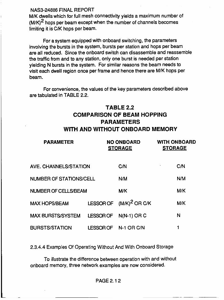
NAS3-24886 FINAL REPORTM/K dwells which for full mesh connectivity yields a maximum number of
(M/K) 2 hops per beam except when the number of channels becomes
limiting it is C/K hops per beam.
For a system equipped with onboard switching, the parameters
involving the bursts in the system, bursts per station and hops per beamare all reduced. Since the onboard switch can disassemble and reassemble
the traffic from and to any station, only one burst is needed per station
yielding N bursts in the system. For similar reasons the beam needs to
visit each dwell region once per frame and hence there are M/K hops perbeam.
For convenience, the values of the key parameters described aboveare tabulated in TABLE 2.2.
TABLE 2.2COMPARISON OF BEAM HOPPING
PARAMETERSWITH AND WITHOUT ONBOARD MEMORY
PARAMETER NO ONBOARD
STORAGE
WITH ONBOARD
_TORAGE
AVE. CHANNELS/STATION C/N C/N
NUMBER OF STATIONS/CELL N/M N/M
NUMBER OF CELLS/BEAM
MAX HOPS/BEAM
MAX BURSTS/SYSTEM
BURSTS/STATION
LESSOR OF
LESSOR OF
LESSOR OF
M/K
(M/K) 2 OR C/K
N(N-1 ) OR C
N-1 OR C/N
M/K
M/K
N
1
2.3.4.4 Examples Of Operating Without And With Onboard Storage
To illustrate the difference between operation with and without
onboard memory, three network examples are now considered.
PAGE 2. 1 2
NAS3-24886 FINAL REPORT
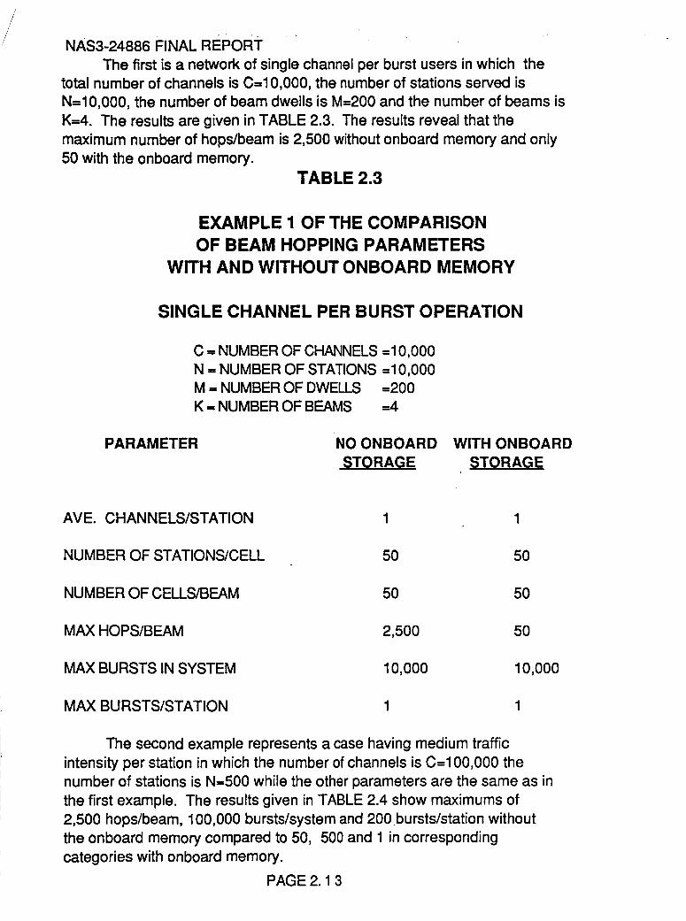
The first is a network of single channel per burst users in which the
total number of channels is C=10,000, the number of stations served is
N=10,000, the number of beam dwells is M=200 and the number of beams is
K=4. The results are given in TABLE 2.3. The results reveal that the
maximum number of hops/beam is 2,500 without onboard memory and only
50 with the onboard memory.
TABLE 2.3
EXAMPLE 1 OF THE COMPARISON
OF BEAM HOPPING PARAMETERS
WITH AND WITHOUT ONBOARD MEMORY
SINGLE CHANNEL PER BURST OPERATION
C = NUMBER OF CHANNELS =10,000
N = NUMBER OF STATIONS =10,000
M = NUMBER OF DWELLS =200
K = NUMBER OF BEAMS =4
PARAMETER NO ONBOARD WITH ONBOARD
STORAGE _TORAGE
AVE. CHANNELS/STATION 1 1
NUMBER OF STATIONS/CELL 5O 5O
NUMBER OF CELLS/BEAM 5O 50
MAX HOPS/BEAM
MAX BURSTS IN SYSTEM
MAX BURSTS/STATION
2,500 50
10,000 10,000
1 1
The second example represents a case having medium traffic
intensity per station in which the number of channels is C=100,000 the
number of stations is N=500 while the other parameters are the same as in
the first example. The results given in TABLE 2.4 show maximums of
2,500 hops/beam, 100,000 bursts/system and 200 bursts/station without
the onboard memory compared to 50, 500 and 1 in corresponding
categories with onboard memory.
PAG E 2. 1 3
NAS3-24886 FINAL REPORTTABLE 2.4
EXAMPLE 2 OF THE COMPARISON
OF BEAM HOPPING PARAMETERS
WITH AND WITHOUT ONBOARD MEMORY
MEDIUM ROUTE INTENSITY
C = NUMBER OF CHANNELS =100,000
N = NUMBER OF STATIONS =500
M = NUMBER OF DWELLS =200
K = NUMBER OF BEAMS =4
PARAMETER NO ONBOARD WITH ONBOARD
STORAGE STORAGE
AVE. CHANNELS/STATION 200 200
NUMBER OF STATIONS/CELL 2.5 2.5
NUMBER OF CELLS/BEAM 50 5O
MAX HOPS/BEAM
MAX BURSTS IN SYSTEM
MAX BURSTS/STATION
2,500 50
100,000 5OO
200 1
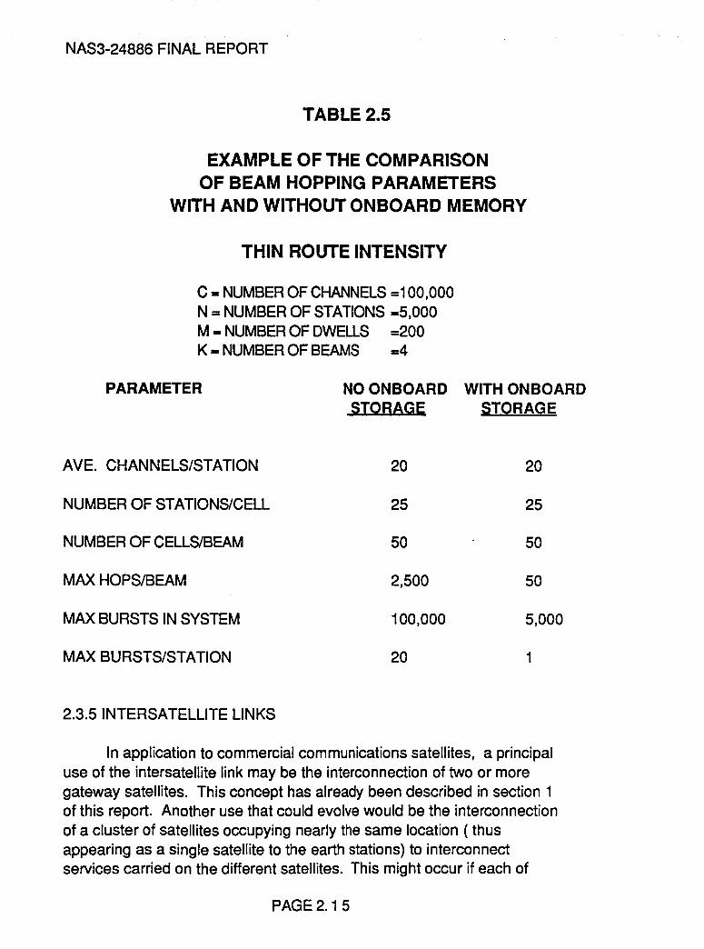
The third example represents a case having thin traffic intensity per
station in which the number of channels is C=100,000 the number of
stations is N=5,000 while the other parameters are the same as in the
first example. The results given in TABLE 2.5 show maximums of 2,500
hops/beam, 100,000 bursts/system and 20 bursts/station without the
onboard memory compared to 50, 500 and 1 in corresponding categories
with onboard memory.
In all three examl_les the presence of onboard memory reduces the
number of bursts carried in the system and the number of beam hops by
orders of magnitude. It is clear that onboard storage has significant value
in a beam hopping system.
PAG E 2. 1 4
NAS3-24886 FINAL REPORT
TABLE 2.5
EXAMPLE OF THE COMPARISONOF BEAM HOPPING PARAMETERS
WITH AND WITHOUT ONBOARD MEMORY
THIN ROUTE INTENSITY
C = NUMBER OF CHANNELS =100,000
N = NUMBER OF STATIONS =5,000
M = NUMBER OF DWELLS =200
K = NUMBER OF BEAMS =4
PARAMETER NO ONBOARD WITH ONBOARD
STORAGE _TORAGE
AVE. CHANNELS/STATION 20 20
NUMBER OF STATIONS/CELL 25 25
NUMBER OF CELLS/BEAM 50 50
MAX HOPS/BEAM
MAX BURSTS IN SYSTEM
MAX BURSTS/STATION
2,500 50
100,000 5,000
20 1
2.3.5 INTERSATELLITE LINKS
In application to commercial communications satellites, a principal
use of the intersatellite link may be the interconnection of two or more
gateway satellites. This concept has already been described in section 1
of this report. Another use that could evolve would be the interconnection
of a cluster of satellites occupying nearly the same location ( thus
appearing as a single satellite to the earth stations) to interconnect
services carried on the different satellites. This might occur if each of
PAG E 2. 1 5
NAS3-24886 FINAL REPORTthe satellites carried a different type of service, such as for example
public telephone on one and land, aero mobile on another, etc. The
intersatellite link would serve to perform cross connects between
services whose transmission modes and implementation architectures are
so different that different satellites are the most economical means for
implementing them. Implementation of an intersatellite link is discussedfurther in section 4.
2.4 TRANSMISSION CONFIGURATIONS
In general, two basic transmission methods have dominated satellite
communications, Frequency Division Multiplexing abbreviated as FDM and
Time Division Multiplexing, abbreviated as TDM. In satellite
communications to connote the fact that the uplinks to the satellite can be
accessed by any number of earth stations and transmissions transponded
from the satellite can be received by any number of stations the
abbreviations are modified to FDMA and TDMA which refer to Frequency
Division and Time Division Multiple Access respectively. This multiple
accessing capability is uniquely the domain of the satellites and must be
used to full advantage to compete with the terrestrial transmission
options.
2.4.1 FDMA
FDMA customarily designates division of the spectrumof a satellite
transponder into a multiplicity of smaller frequency bands each occupied
by a carrier. The carriers may have various bandwidths which are
individually scaled to accommodate different levels of traffic or they may
all be of the same bandwidth as in the case of Single Channel Per Carrier
(SCPC) systems used in DAMA networks such as INTELSAT's SPADE,
INMARSAT's maritime mobile system, SKY SWITCH and PALAPA. It is
likely that the land mobile and aeronautical mobile systems will use this
technique.
2.4.2 TDMA
TDMA refers to the division of a high bit rate carrier, occupying the
entire bandwidth of a transponder, into time division burst transmissions
that eminate from numerous earth stations and are synchronized so that
each arrives at the satellite in an epoch assigned uniquely to it. The
simplest TDMA system uses a bent pipe transponder in which the uplink
transmissions are simply repeated and returned to the earth on the
PAGE 2. 1 6
NAS3-24886 FINAL REPORT
downlink. A multiplicity of transponders can be used in such a system and
the up and down beams can be pointed to different regions to provide
multiple beam connections such as those previously described for
INTELSAT V. Stations can access destinations in different regions by
frequency hopping their transmissions to fall in the band of the
transponder with its downbeam pointed to the desired destination region.
TDMA is inherently suited for systems that perform onboard dynamic
switching. By rule, each station's transmission must arrive and pass
through the satellite in a prescribed time epoch. It is a relatively simple
matter to coordinate these epochs with the switching of the onboard
connections and to have them coincide with the proper switching epoch to
be directed to the destination downbeam. As explained previously, this is
what happens in the INTELSAT Vl when it uses its MSM to operate in the
SS-TDMA mode. This also is done for satellites that will perform
memoryless onboard switching at baseband such as currently planned onthe ITALSAT.
TDMA is also used on the ACTS satellite which incorporates an
onboard baseband switch that stores the individual channel signals
arriving on the uplinks from multiple uplink hopping beams in inputmemories and rearranges these into TDM downlink transmissions that
contiguously group all of the traffic destinated to a dwell region into an
epoch that coincides with the time that the downlink hopping beam pointsto the destination.
2.4.3 MF/TDMA
There is another way to use TDMA that is referred to as M F/TDMA.
simply refers to the the transmission of several TDMA carriers in a
transponder rather than one. These carriers are used simultaneously by
different stations to carrier their burst transmissions. The advantage is a
reduction in the amount of transmit power needed by an earth station to
access the network. The disadvantage is the reduction of the space
segment's capacity because of the transponder output backoff allowance
needed to reduce intermodulation distortion to an acceptable level.
Typically, between 30 and 50% of the space segment capacity must be
given up to achieve the MF/TDMA operation in a bentpipe transponder.
It
MF/TDMA can also operate in an satellite switched mode
(SS-MF/TDMA) in which TDMA traffic bursts operating on multiple low
burst rate carriers through the MSM.
PAGE 2. 1 7
NAS3-24886 FINAL REPORTMF/TDMA can also be used in baseband switched systems, most likely
on the uplinks. For example, the bandwidth normally allocated to thehighest bit rate (or symbol rate) TDMA carrier may be assigned to severallower bit rate (or symbol rate) TDMA carriers. This is done in the ACTSwhere the upbeams can carry either one 110 Msym/s or four 27.5 Msym/sTDMA carriers. In this case, because onboard demodulation andremodulation (regeneration)is used, there is no space segment powerbackoff penalty.
2.4.4 CDMA
Another transmission method that has been used principally by the
military is Code Division Multiplexing which when used on the satellites
can be termed as Code Division Multiple Access (CDMA). CDMA uses unique
codes to distinguish the transmissions of the individual stations of the
network. Each stations is assigned a unique orthogonal code that is
decoded at its receive side. To call any particular station, a transmitter
sends the message coded in the desired receiver's code. Many such
transmissions can be sent simultaneously to serve a large number of
stations. The system is limited in the number of coded transmissions that
can be simultaneously supported by the noise background generated by thecumulative addition of all of the transmissions at the receivers. CDMA
systems are thus said to be self noise limiting. CDMA also has an
attending property that causes the transmitted signal to be spread over a
spectrum that can be orders of magnitude greater than that which would
be occupied if the signal were transmitted by ordinary means: This
property is due to the fact that each symbol of the message is coded in
terms of M symbols of a coding pseudo random bit sequence which causes
the spectrum of the coded signal to be multiplied in width by M. The bits of
the pseudo random code are frequently referred to as chips. This spreading
action dilutes the spectral density of the transmitted signal M "1 by and
can reduce the signal spectrum level to a level less than the thermal noise
background to hide the signal from unwanted listeners. This is called the
spread spectrum action. Obviously, this same spread spectrum action can
reduce a high power signal's spectral density to a level that is non
interfering to other services sharing the same band.
CDMA has not been used to any significant extent in satellite
systems mostly because greater transmission capacities can be achieved
by FDMA and TDMA using the same facilities. However, there is an
application of CDMA that has received considerable attention in the last
few years as implemented by the Equatorial Radio Company. In this case
the Coded transmission is used principally for its attending property to
PAG E 2. 1 8
NAS3-24886 FINAL REPORT
spread the transmitted signal over a wide spectrum. In this way a high
power signal can be transmitted from a small antenna with low spectral
density and thereby avoid violating the spectral density limits set forth by
the CCIR. This makes it possible to operate small earth stations at C bandin environments where clearance could not otherwise be obtained. On the
receive side, CDMA also has the advantage of permitting signals coded in
the station's code to be picked out of an environment of interfering
narrowband signals. This is the result of the correlation receive
processing that literally converges the coded receive signal into a
narrowband signal of bandwidth determined by the original uncoded signal
while spreading the interfering signal's power over a wideband equal to or
greater than that of the spectrum spread signal.
In this study, only FDMA, TDMA and MF/TDMA transmission methods
are assumed. CDMA has its peculiar advantages which can be factored in
on a case by case basis as the need dictates.
2.4.5 TRANSMISSION CONFIGURATIONS
Various arrangements of FDMA, TDMA and MF/TDMA transmission can
be used in a satellite system. Transmission schemes are the principal
distinguishing hallmarks of the various classes of networks that will use
future satellites which have multiple beams some of which are fixed and
others hopping. Transmission methods applicable to Uplink and Downlink
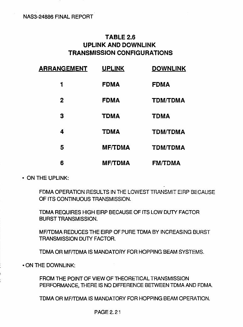
respectively are listed in the columns of TABLE 2.6. Each row identifies a
particular combination of transmission methods for the up and down links
respectively.
2.4.5.1 FDMA-FDMA Operation
Arrangement 1 uses FDMA on both the up and down links. It is the
principal method used for most satellite systems during their first two
decades of existence. The method is the natural evolutionary product of
the use of the global and regional beam bent pipe transponding repeater
satellite. It is also used as the principal transmission method in the
multibeam systems of INTELSATs V and VI. It's attractiveness resides in
the freedom it offers in terms of the operating discipline that must be
adhered to by the users of the system. This freedom has led to the growth
of many different and novel network architectures (such as the node/hub
star networks popular at this time for VSAT business communications)
and for this reason it will continue to be a principal component of any
satellite system in the immediate future. The recent Hughes Galaxy filing
for a CONUS system uses a combination of four regional up beams
PAGE 2. 1 9
NAS3-24886 FINAL REPORT
frequency cross connected to 64 fan-shaped downbeams distributed suchthat 16 fall into each upbeam region to support FDMA carriers carrying 64kb/s SCPC services and TI digital services.
The principal difficulties with FDMA methods are the transponder
distortion limitation and cumbersome interconnectivity. The distortion
limitation is caused by the interaction of multiple FDMA carriers that
share a single transponder. To reduce the distortion products so that they
do not limit the performance of the link, it is necessary to back-off the
power output of the transponders TWTA or SSPA by 3 to 5 dB. This wastes
the valuable commodity of power for which millions of dollars have been
invested. Connectivity is no problem for FDMA as long as all stations of a
network are contained within the same beam. Multibeam networks
multiply the number of FDMA carriers needed to accomplish full
connectivity by the number of beams. This is not the case for TDMA.
PAGE 2.2 0
NAS3-24886 FINAL REPORT
TABLE 2.6
UPLINK AND DOWNLINK
TRANSMISSION CONFIGURATIONS
ARRANGEMENT UPLINK DOWNLINK
1 FDMA FDMA
2 FDMA TDM/TDMA
3 TDMA TDMA
4 TDMA TDM/TDMA
5 MFFFDMA TDM/'FDMA
6 MF/'rDMA FMFrDMA
• ON THE UPLINK:
FDMA OPERATION RESULTS IN THE LOWEST TRANSMIT EIRP BECAUSE
OF ITS CONTINUOUS TRANSMISSION.
TDMA REQUIRES HIGH EIRP BECAUSE OF ITS LOW DUTY FACTOR
BURST TRANSMISSION.
MF/'I'DMA REDUCES THE EIRP OF PURE TDMA BY INCREASING BURST
TRANSMISSION DUTY FACTOR.
TDMA OR MF/TDMA IS MANDATORY FOR HOPPING BEAM SYSTEMS.
• ON THE DOWNLINK:
FROM THE POINT OF VIEW OF THEORETICAL TRANSMISSION
PERFORMANCE, THERE IS NO DIFFERENCE BETWEEN TDMA AND FDMA.
TDMA OR MF/TDMA IS MANDATORY FOR HOPPING BEAM OPERATION.
PAGE 2. 21
NAS3-24886 FINAL REPORT
Dynamic time domain switching and beam hopping cannot be used
with FDMA to achieve beam to beam connectivity because the
transmissions are inherently continuous. To achieve full beam to beam
connectivity, it is necessary to slice up the spectrum into bands and to
incorporate banks of filters onboard the satellite to frequency cross
connect the beams. In a network having K beams, full connectivity
requires that each of the K up beams be cross connected to K down beams.
This requires K2 cross connections and as many individual filters. The
immensity of the cross connect problem is illustrated by considering the
interconnection of a 200 beam system to fully interconnect CONUS which
would require 40,000 filters. The cross connect bandwidths would be very
small and the implementation of that many filters onboard impractical.
Yet another limitation exists in the inflexibility of the traffic
distribution. Once the bandwidths are established, they are not easily
modified to accommodate changes in the distribution. By formulating
special configurations of beam coverages and cross connects it is possible
to achieve reasonable multibeam compromises for FDMA distribution. The
INTELSAT V is a good example of this.
The recent GALAXY configuration offered by Hughes for FDMA service
uses four approximately quarter CONUS uplink beams each connected to
sixteen 1/64th CONUS fan beams (four in each of the uplink beam regions)
requiring a total of 64 filters to achieve the cross connections. This is a
reasonable number. The limitations of this arrangement reside in the fact
that to be used efficiently the traffic must conform to a fairly rigid
distribution that is literally built into the satellite system design. Also
the improvement in the uplink G/T is limited to only 6 dB compared to the
full CONUS and the downlink eirp increase attributed to beam gain is
limited to 12 dB compared to CONUS.
2.4.5.2 FDMA-TDM/TDMA Operation.
Arrangement 2 employs continuous FDMA transmissions on the
uplinks and TDM or TDMA on the downlinks. It is an optimum mode of
operation from the point of view of most efficient use of the downlinks
jointly with the most efficient use the earth stations if each transmits
only one carrier. The earth stations operate in continuous transmission
mode which with a single carrier per HPA uses the power potential of the
HPA with greatest efficiency. The satellite operates in a single carrier
per transponder time division multiplexed mode that allows it to
distribute the uplink signals to all destinations without output power
backoff or the need to provide many modulator/HPA units for numerous
PAG E 2. 2 2
NAS3-24886 FINAL REPORT
downlink FDMA carriers. However, the earth stations must operate in an
asymmetrical manner for this configuration, the uplinks being continuous
FDMA and the down links TDMA. The bit rate will be much higher on the
downlink. Except for the need to implement a high speed demodulator this
higher downlink rate does not change the downlink transmission budgets.
This is so because, assuming the same total power delivered by the
satellite to the composite of down links, the energy per bit on thedownlink is the same whether the transmission is a low bit rate FDMA
continuous carrier or a TDMA burst supporting the same bit rate destined
to the station. Because TDM/TDMA always operates using single carrier
per transponder, it may actually provide a better downlink budget
compared to FDMA since output power backoff is avoided.
2.4.5.3 TDMA-TDMA Operation
Arrangement 3 refers to TDMA operation via bent pipe transponders.
This is the operating configuration currently used for all TDMA systems. A
good example is the 120 Mb/s TDMA system in the INTELSATs V and VI.
The 72 MHz bandwidth transponders operate in a single carrier per TWTA
mode resulting in very efficient use of the transponder's power resource.
Inherently, the uplink and downlinks must be the same since the burst
transmissions simply pass through the satellite without processing. By
the use of transponder hopping, performed at the earth stations by
transmitting their bursts on designated frequencies at designated times,
the composition of station bursts carried in the down beams is different
from that carried in the up beams. This is accomplished by adjusting the
earth station burst time plans that specify the time and frequency of
transmission and reception of the TDMA bursts for each station. These
burst time plans are generated by INTELSAT traffic management and sent
to the earth stations of the entire network over TDMA control (order wire)
channels. The time plans of all stations are changed in a synchronized
manner by use of a coordinated burst time plan change countdown. This
causes the simultaneous switchover from an old to a new time plan in thesame TDMA frame for all stations.
In the INTELSAT Vl, the number of beams is increased from 4 to 6
and two dynamic microwave switch matrices (MSM), each interconnecting
a bank of six 72 MHz bandwidth transponders, are provided to fully
interconnect the beams. When TDMA is used jointly with the satellite it is
referred to as SS-TDMA. The dynamic MSMs permit full interconnectivity
of the 6 beams without the need to perform frequency hopping. The earthstations use the same TDMA terminals as were used in the INTELSAT V.
The switching of the MSM is performed in terms of states of the switch
PAGE 2. 23
NAS3-24886 FINAL REPORT
that remain static for epochs long enough to pass the traffic scheduled forthe state. Such switch states are illustrated in Figure 2.5. Theoreticallyan upper bound to the number of switch states needed during each TDMAframe to achieve better than 95% efficient traffic fill is given by theexpression K2-2K +2 where K is the number of beams. For K,.6, thisnumber is 26. Approximately twice this number is actually provided to
accommodate burst hopping between the switches and other unforeseen
contingencies. The satellite switch needs a switch state time plan that is
associated with the burst time plans for the earth stations. Both of these
time plans are included in the coordinated time plan procedure to
synchronize changes in the switch state time plan with those in the
traffic time plan. SS-TDMA operation equates to a distributed switching
machine in which time domain storage is performed in the earth stations
and memoryless space switching is performed on the satellite.
2.4.5.4 TDMA-TDM/TDMA Operation
This mode of operation, designated as arrangement 4, is possible
only when there is a baseband processor on board the satellite. The uplink
signals are assumed to be carried in the conventional TDMA fashion as
described above. However, on the downlink the uplink signals are
multiplexed into a contiguous TDM stream. This can be accomplished by
means of the onboard baseband processor which converts the TDMA bursts
arriving on the uplinks into their digital baseband form and, by means of
either onboard buffers or onboard circuit switching with memory,
multiplexes these on to the continuous downlink TDM streams. If the
downlink beams are stationary then the downlink transmission appears
continuous thus simplifying the earth station's demodulator and receive
side demultiplexer. The ITALSAT system uses this design. If the downlink
uses hopping beams then eventhough the transmission is continuous, it
appears in burst format (like TDMA) in the individual beam dwells. The
ACTS system uses this design.
2.4.5.5 MF/TDMA-TDM/TDMA Operation
This mode of operation,designated as arrangement 5, uses the same
downlink design as arrangement 4; however, on the uplink it introduces
multiple, low bit rate uplink TDMA carriers which are referred to as
MF/TDMA. This type of implementation requires an onboard baseband
processor that is able to demodulate the low bit rate uplink TDMA signals
and recombine them into a composite high bit rate TDM (in the case of
fixed beams) or TDMA (in the case of hopping beams) carrier. The
advantage of this arrangement is that it makes it possible to use less eirp
PAGE 2. 2 4
NAS3-24886 FINAL REPORT
to operate the uplink permitting the use of earth stations having smallerantennas or lower power HPAs or both. A necessary precaution is that theuplink rate must be high enough to serve the composite traffic of areasonable number of earth stations. Also, the transmit side burst ratewill be higher than the receive side burst rate making it difficult to testthe earth station in a local loop back connection. ACTS also operates inthis mode.
2.4.5.6 MF/TDMA-MF/TDMA Operation
Arrangement 6 applies to operating multiple low burst rate TDMA carriersin the band of a transponder rather than a single and much higher burstrate TDMA carrier. It applies only in the case of bent pipe operation whereindividual transponders, used to interconnect the up and downbeams,operating in either a static or dynamic switched mode, carry several lowburst rate TDMA carriers shared among the earth stations rather than onehigh burst rate TDMA carrier. An example of this operation would be theuse of the HBR MSM transponders of ACTS to carry a multiplicity of low bitrate TDMA carriers in SS-MF/TDMA with or without beam hopping. Suchoperation sacrifices capacity but permits access by much smaller earthstations than would otherwise be possible.
PAGE 2. 2 5

NAS3- 24886 FINAL REPORT
2.5 COMPUTER AND DATA COMMUNICATIONS
To establish a departure baseline for Computer and Data
Communications, an analysis was made of the possibilities for handling
packet data using the onboard configuration presently planned for the
ACTS. There are several ways that packet data communications can be
supported with the present ACTS multibeam communications processing
package to provide node-hub, and full mesh packet connectivities. These
are discussed in the following. Because the ACTS MCP has no onboard
processing capability for interpreting the packet header information, it
cannot be used as a packet node and can act only as a path through which
the packets pass without modification. This path may be circuit switched
or stationary and with these capabilities the ACTS MCP can support packet
communications between nodes in a mesh configuration or between nodes
and hubs in a star configuration.
2.5.1 PACKET COMMUNICATIONS ON ACTS
The ACTS system can support experimental studies of packet
communications on board satellites by means of its onboard BBP as
controlled by the ACTS MCS. This can be accomplished in a circuit
switched manner or over a stationary preassigned channels used in a
random access TDMA (slotted Aloha) fashion. A packet node onboard is a
future possibility and has important operational advantages due to direct
multidestinational distribution which is possible only with a satellite,
and reduced propagation delay in performing the acknowledgement
function. The present ACTS is not equipped with an onboard packet node
capability; however, when used in the circuit switched packet mode it can
provide valuable experience in studying the protocols needed for such
operation.
2.5.1.1 Circuit Switched Operation
In the circuit switched mode a 64 kbit/s channel is set up in each
direction between the origin and the destination over the ACTS Multibeam
Communications Payload (MCP). Control of the stored messages is
performed from the ground by the MCP using a high rate data link to the
satellite. This permits network control of onboard packet communications
experiments from the ground via the order wire links between sending
node and the MCP and the receiving node and the MCP. The various steps
needed to accomplish packet communications using this arrangement are
PAGE 2.2 6
NAS3' 24886 FINAL REPORT
as follows:
1) Receive and store packet at the earth station node,
2) Request satellite forward and return channels to destination from
MCS via orderwire,
3) Using a synchronous burst time plan change procedure establish the
channels and transmit the packet,
4) Destination station receives the packet and performs an error
check. If correct, it responds with an acknowledgement. If in error,
no acknowledgement is sent,
5) If no acknowledgment is received at the originating station within
an established timeout, the packet is retransmitted until an
acknowledgement is received.
6) When an acknowledgement is received at the originating station, it
sends a channel disconnect message to the MCS via the orderwire.
2.5.1.2 Stationary Preassigned Channel Operation
In a preassigned stationary configuration, permanent channels are
established via the ACTS MCS which connect upbeam dwells to downbeam
dwells and these are accessed by the earth stations on a random access
TDMA basis using the slotted Aloha packet communications mode. This
arrangement is illustrated in Figure 2.6 for the connection of an uplink
channel in each of 4 beam dwell regions to 4 downlink channels in one
downlink channel which is in this case in beam dwell region 1. In this
figure the channels are designated by pairs of numbers, the first
designating the dwell region and the second the channel number in that
dwell occurring in increasing numerical order. The same connectivity
pattern can be repeated for any number of down beams (not shown in the
diagram). For total connectivity, if the the hopping beam system has N
dwell regions that are visited in each 1 ms TDMA frame and it is desired to
interconnect all N in a random access TDMA manner, N uplink channels
would be assigned to each dwell, one destined to each of N downlink
dwells, and N downlink channels would be assigned in each downlink dwell.
Thus a total of N2 channels would be used to support the system. Such a
configuration can carry approximately 20% of the maximum capacity in the
form of random packets synchronized to slot boundaries (the slotted Aloha
PAG E 2.2 7

NAS3- 24886 FINAL REPORT
mode). Hence the throughput capacity of the system would be 0.2Nx64
kbit/s. Assuming that N = 20 and that each transaction requires a 1 kbit
packet in the forward direction and al00 bit transaction in the reverse
direction, the configuration would support 40000 transactions per day. If
a node/hub arrangement in which uplinks from several dwell regions are
routed to only one downlink in a destination dwell region containing the
hub, a return link must be provided to all originating nodes from the dwell
region containing the hub and this can be accomplished by broadcasting the
uplink from the hub's dwell.
Stationary preassigned operation can also be configured to provide
the uplink channels in a serial fashion in a superframe. This permits
operation of random access TDMA with a lesser commitment of total
capacity than does the configuration described in the previous paragraph.
A single downlink channel in a destination dwell region is time division
multiplexed among the uplink beam dwells in a superframe as shown in
Figure 2.7. This pattern can be repeated for a downlink in each
destination dwell to achieve full interconnectivity using the capacity of N
channels. Such a configuration is shown in Figure 2.8 for N=4.
2.5.1.3 Future Onboard Packet Node
An attractive communications concept involving future satellites
with on board baseband processing capability uses the satellite as a
packet communications node. In this application the satellite BBP must
perform the following steps:
1) Receive packets from earth station nodes,
2) Store the packets in its memory,
3) Read the address information,
4) Send acknowledgments to the sending nodes,
5) Forward the packets to an earth station node near the destination,
6) Wait for acknowledgements, and
7) Remove acknowledge packets from its memory.
PAGE 2.2 8
NAS3- 24886 FINAL REPORT
The ACTS communications system as it is now configured does not havethe capability to perform the packet error check and acknowledgementonboard, and hence these functions must be performed at the destinationearth station. However these functions can be executed via the MCS
function at the NASA ground station operating in a manner that assigns aswitched circuit to carry the packet. Of course this type of operationinvolves more delay, principally double hop link rather than a half singlehop, but it can provide a means to develop protocols and gain operatingexperience in implementing an onboard packet node function.
The most obvious extension of an advanced onboard processing
satellite network controller beyond that of the ACTS for accommodating
computer and data communications is the provision of node processing
capabilities on board the satellite. This option is considered in the nextsection.
2.5.2 CONFIGURATIONS FOR COMPUTER AND DATA COMMUNICATIONS
Three methods for configuring computer and data communications
over a satellite equipped with an onboard processing and beam hopping
capability are discussed in the following. The first uses a circuit
switched technique, the second random access with preassigned circuits
routed on the satellite and the third incorporates a packet node onboard
the satellite. First, it is important to demonstrate the advantages of
having such a capability compared to the more simple routing through
circuit switched paths as is possible on the ACTS. Important factors to be
considered are onboard packet acknowledgements and distribution of such
packets directly to their destinations. Secondly, assuming that
advantages are identified, it is important to assess and select an
implementation technology.
2.5.2.1 Circuit Switched Operation
In a circuit switched mode, a full duplex circuit is established
between the origin and the destination. This is accomplished by using the
signalling order wires that exist between the traffic stations and the
Network Control Center (NCC) facility. When a data transmission session
is to be initiated, the originating station requests a duplex circuit by
informing the NCC of the destination telephone number. The NCC proceeds
to fulfill the request by identifying appropriate time slots in the burst
time plans of the originating and destination stations and routing through
the satellite switch including the hopping beam dwell assignments. The
PAGE 2.2 9
NAS3- 24886 FINAL REPORT
NCC commands the execution of these instructions, the circuit is
established and the data transmission proceeds. When the session is
completed, the originating station indicates the termination to the NCC
and the circuit is disconnected.
The various time steps and the delay times encountered in the process
of establishing, operating and terminating such a circuit are illustrated in
the time graph of Figure 2.9. The four columns of this figure refer
respectively to the functions performed at 1) the originating earth
station, 2) onboard the satellite, 3) the NCC and 4) the destinationstation. The vertical axis is annotated with the number of the function
performed and the elapsed time between the execution of functions due to
propagation delay and processing latency. The propagation delay on a
single pass between the satellite and the earth is assumed to range from
120 to 140 ms.
At time I a switched circuit session for data transmission is
initiated by a circuit request message (CRM) to the NCC which identifies
both the originating and destination interfaces. At time 2 the CRM passes
through the satellite over an established orderwire path and hence to the
station that serves the NCC.
At time 3, the CRM is received by the NCC where the channels are
selected for routing the call over the system. The NCC organizes a channel
assignment message (CAM) which identifies the channels to be used by the
originating and destination stations and transmits this to the stations
over an appropriate network control channel. It also organizes a satellite
switch message that controls the channel routing through the satellite and
sends this to the satellite over its network control link. Both of these
messages pass through the satellite at about the same time at time 4. The
satellite switch message initiates onboard a coordination delay timer that
causes the satellite switch to assume the new switch configuration on a
time precisely synchronized with the arrival at the satellite of the newly
configured channels that have been set up at the originating and
destination stations in response to the CAM. The CAM is received at both
the originating and destination stations at about the same time at time 5
and using an appropriate delay of no greater than 20 ms at each to
compensate for propagation path length differences the duplex circuit is
established for transmission at time 6. The time elapsed from the request
at time 1 to the circuit availability at time 6 is a maximum of 580 ms and
a minimum of 500 ms. At time 6, the data transmission can commence.
PAGE 2.3 0
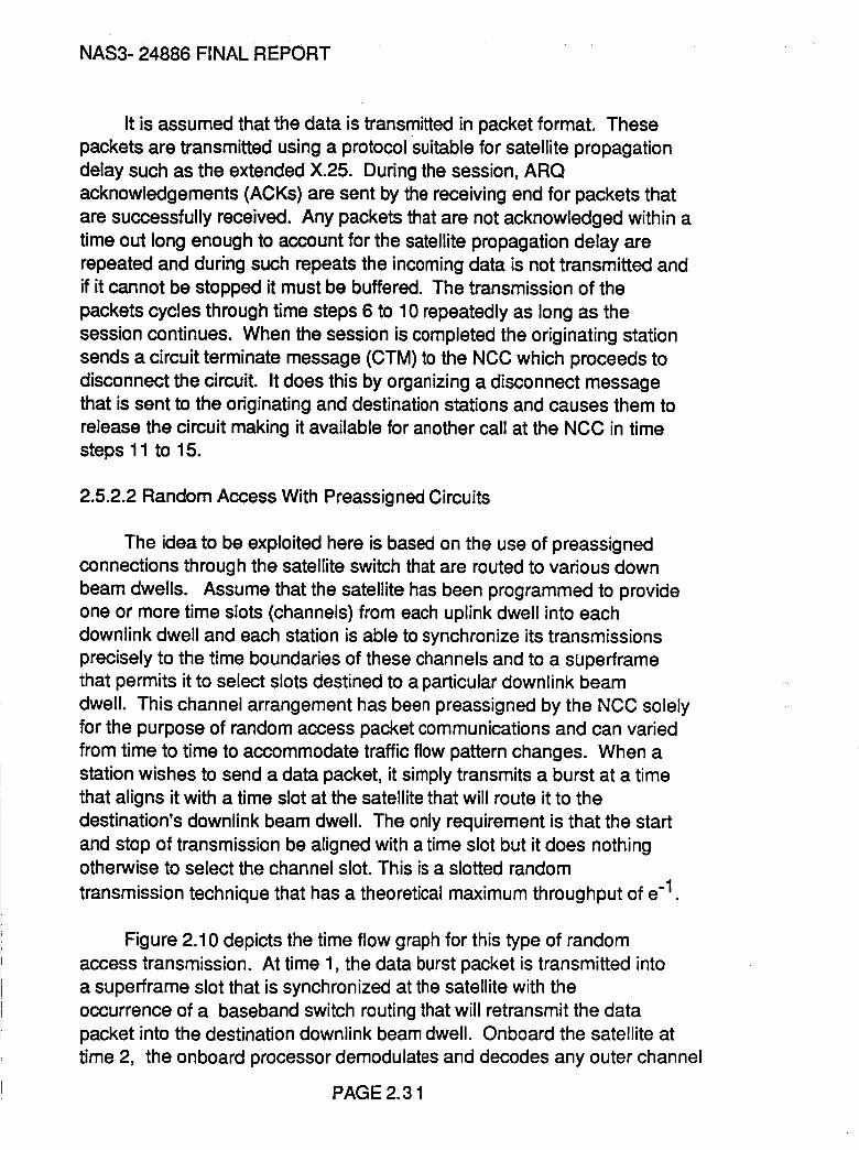
NAS3- 24886 FINAL REPORT
It is assumed that the data is transmitted in packet format. These
packets are transmitted using a protocol Suitable for satellite propagation
delay such as the extended X.25. During the session, ARQ
acknowledgements (ACKs) are sent by the receiving end for packets that
are successfully received. Any packets that are not acknowledged within a
time out long enough to account for the satellite propagation delay are
repeated and during such repeats the incoming data is not transmitted and
if it cannot be stopped it must be buffered. The transmission of the
packets cycles through time steps 6 to 10 repeatedly as long as the
session continues. When the session is completed the originating station
sends a circuit terminate message (CTM) to the NCC which proceeds to
disconnect the circuit. It does this by organizing a disconnect message
that is sent to the originating and destination stations and causes them to
release the circuit making it available for another call at the NCC in time
steps 11 to 15.
2.5.2.2 Random Access With Preassigned Circuits
The idea to be exploited here is based on the use of preassigned
connections through the satellite switch that are routed to various down
beam dwells. Assume that the satellite has been programmed to provide
one or more time slots (channels) from each uplink dwell into each
downlink dwell and each station is able to synchronize its transmissions
precisely to the time boundaries of these channels and to a superframe
that permits it to select slots destined to a particular downlink beam
dwell. This channel arrangement has been preassigned by the NCC solely
for the purpose of random access packet communications and can varied
from time to time to accommodate traffic flow pattern changes. When a
station wishes to send a data packet, it simply transmits a burst at a time
that aligns it with a time slot at the satellite that will route it to the
destination's downlink beam dwell. The only requirement is that the start
and stop of transmission be aligned with a time slot but it does nothingotherwise to select the channel slot. This is a slotted random
transmission technique that has a theoretical maximum throughput of e -1 .
Figure 2.10 depicts the time flow graph for this type of random
access transmission. At time 1, the data burst packet is transmitted into
a superframe slot that is synchronized at the satellite with the
occurrence of a baseband switch routing that will retransmit the data
packet into the destination downlink beam dwell. Onboard the satellite at
time 2, the onboard processor demodulates and decodes any outer channel
PAGE 2.3 1
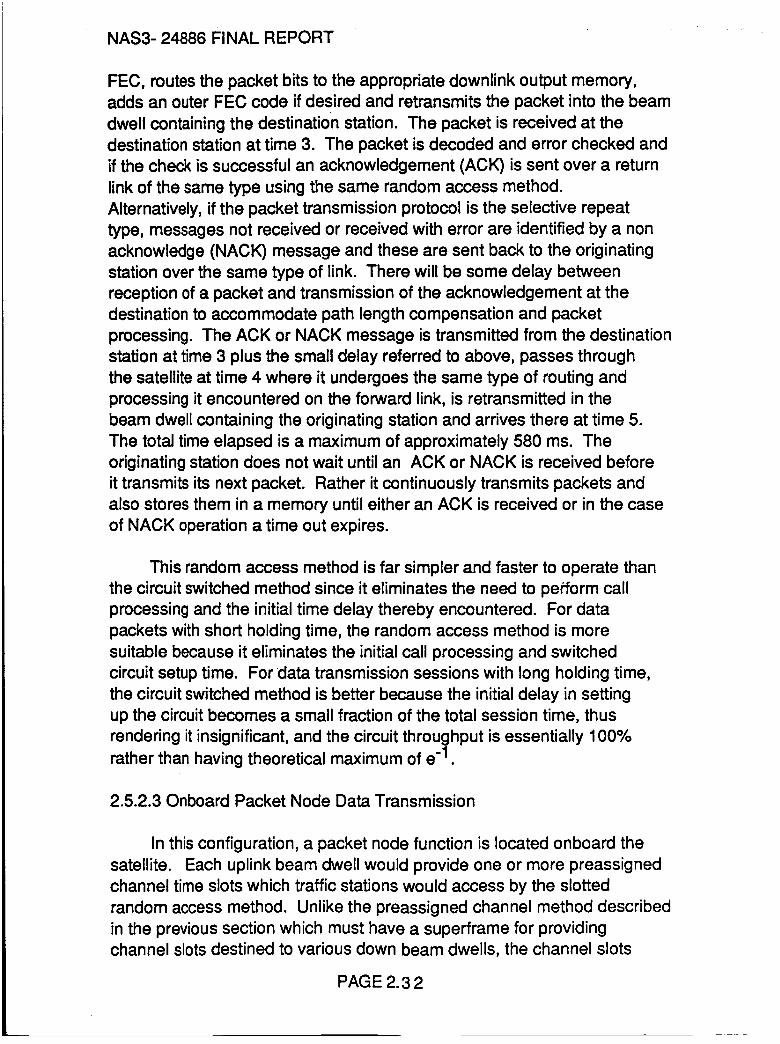
NAS3- 24886 FINAL REPORT
FEC, routes the packet bits to the appropriate downlink output memory,
adds an outer FEC code if desired and retransmits the packet into the beam
dwell containing the destination station. The packet is received at the
destination station at time 3. The packet is decoded and error checked and
if the check is successful an acknowledgement (ACK) is sent over a return
link of the same type using the same random access method.
Alternatively, if the packet transmission protocol is the selective repeat
type, messages not received or received with error are identified by a non
acknowledge (NACK) message and these are sent back to the originating
station over the same type of link. There will be some delay between
reception of a packet and transmission of the acknowledgement at the
destination to accommodate path length compensation and packet
processing. The ACK or NACK message is transmitted from the destination
station at time 3 plus the small delay referred to above, passes through
the satellite at time 4 where it undergoes the same type of routing and
processing it encountered on the forward link, is retransmitted in the
beam dwell containing the originating station and arrives there at time 5.
The total time elapsed is a maximum of approximately 580 ms. The
originating station does not wait until an ACK or NACK is received before
it transmits its next packet. Rather it continuously transmits packets and
also stores them in a memory until either an ACK is received or in the case
of NACK operation a time out expires.
This random access method is far simpler and faster to operate than
the circuit switched method since it eliminates the need to perform call
processing and the initial time delay thereby encountered. For data
packets with short holding time, the random access method is more
suitable because it eliminates the initial call processing and switched
circuit setup time. For data transmission sessions with long holding time,
the circuit switched method is better because the initial delay in setting
up the circuit becomes a small fraction of the total session time, thus
rendering it insignificant, and the circuit throu_]hput is essentially 100%rather than having theoretical maximum of e".
2.5.2.30nboard Packet Node Data Transmission
In this configuration, a packet node function is located onboard the
satellite. Each uplink beam dwell would provide one or more preassigned
channel time slots which traffic stations would access by the slotted
random access method. Unlike the preassigned channel method described
in the previous section which must have a superframe for providingchannel slots destined to various down beam dwells, the channel slots
PAGE 2.3 2
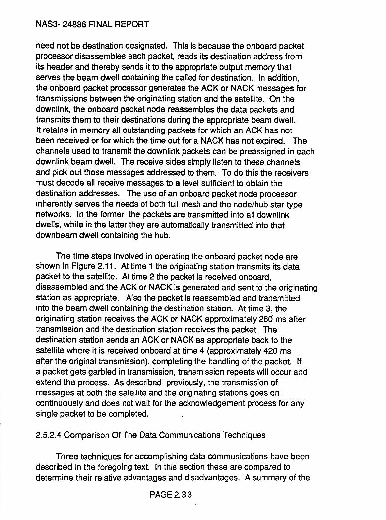
NAS3- 24886 FINAL REPORT
need not be destination designated. This is because the onboard packetprocessor disassembles each packet, reads its destination address fromits header and thereby sends it to the appropriate output memory thatserves the beam dwell containing the called for destination. In addition,the onboard packet processor generates the ACK or NACK messages fortransmissions between the originating station and the satellite. On thedownlink, the onboard packet node reassembles the data packets andtransmits them to their destinations during the appropriate beam dwell.It retains in memory all outstanding packets for which an ACK has notbeen received or for which the time out for a NACK has not expired. Thechannels used to transmit the downlink packets can be preassigned in eachdownlink beam dwell. The receive sides simply listen to these channelsand pick out those messages addressed to them. To do this the receivers
must decode all receive messages to a level sufficient to obtain the
destination addresses. The use of an onboard packet node processor
inherently serves the needs of both full mesh and the node/hub star type
networks. In the former the packets are transmitted into all downlink
dwells, while in the latter they are automatically transmitted into that
downbeam dwell containing the hub.
The time steps involved in operating the onboard packet node are
shown in Figure 2.11. At time 1 the originating station transmits its data
packet to the satellite. At time 2 the packet is received onboard,
disassembled and the ACK or NACK is generated and sent to the originating
station as appropriate. Also the packet is reassembled and transmitted
into the beam dwell containing the destination station. At time 3, the
originating station receives the ACK or NACK approximately 280 ms after
transmission and the destination station receives the packet. The
destination station sends an ACK or NACK as appropriate back to the
satellite where it is received onboard at time 4 (approximately 420 ms
after the original transmission), completing the handling of the packet. If
a packet gets garbled in transmission, transmission repeats will occur and
extend the process. As described previously, the transmission of
messages at both the satellite and the originating stations goes on
continuously and does not wait for the acknowledgement process for any
single packet to be completed.
2.5.2.4 Comparison Of The Data Communications Techniques
Three techniques for accomplishing data communications have been
described in the foregoing text. In this section these are compared to
determine their relative advantages and disadvantages. A summary of the
PAG E 2.3 3
NAS3- 24886 FINAL REPORT
three in terms of various system parameters is given in Table 2.7.
Considering first the circuit switched technique designated as case 1. It
has a prominent characteristic which is the 500 and 580 ms delay
encountered in connecting and disconnecting the circuit that under certain
circumstances can be a disadvantage. This delay results in low throughput
efficiency when the data transmission has a short holding time. For
example if a single 1 kbyte packet is to be transmitted over a 64kbit/s
circuit, the holding time is only 62.5 ms. Obviously, if it takes 580 ms to
setup the circuit and an equal time to take it down, then the total time to
serve the message is 1222.5 ms yielding a throughput efficiency of only
5%. However, if the session holding time is long compared to the time
required to setup and disconnect the circuit, then the efficiency can be
much higher. For comparison, the maximum efficiency of a slotted packet
system is e"1 (37%). The length of session that yields a switched circuit
throughput efficiency of this value is 670 ms. or approximately 10 1
kbyte packets. From the point of view of flexibility, the circuit switched
method is rated as good because it is able to establish a circuit anywhere
in the network. With regard to earth station complexity, it requires the
equipment and protocols needed to perform call processing and the
communications link back to the NCC. Such equipment and protocols are
not necessary in the random access packet modes. With regard to onboard
equipment complexity, it requires a demultiplexing/demodulation
/decoding/circuit switching/coding/modulation/multiplexing capability
which is of the order of complexity of the ACTS.
Consider next case 2 which incorporates random access data
transmission with preassigned channels. A principal disadvantage of this
configuration resides in the requirement that for full connectivity in an N
beam dwell system, N channel slots (one to each down beam dwell) must
be provided in each upbeam dwell yielding a total of N 2 upbeam channel
slots. Thus, a large fraction of system capacity is used to implement this
configuration. Because the channel used to carry the packets is
preassigned, it is always available and no delay is encountered to connect
and disconnect. This results in high throughput efficiency for data calls
with short holding times. The throughput efficiency is theoretically
limited to a maximum of e "1 where congestion on the transmission link
causes so many packet collisions that the system crashes. In actual
practice, the throughput is limited to about 20% to achieve satisfactory
performance. Even so the use of this type of data communications is
becoming one of the most popular for satellite bypass of the terrestrial
networks especially by users who transmit only a few packets at a time a
few times a day. The network flexibility, which refers to the ability to
PAG E 2.3 4
NAS3- 24886 FINAL REPORT
adjust transmission capacity to the traffic flow pattern, is relatively
• poor compared to that possible with circuit switching. Consequently, the
capacity between some up and down links, if under utilized, is not rapidly
reassignable. This is not an unreconcilable limitation since if the
terminals are equipped for burst time plan reconfiguration under control
of the NCC, provision can be made to reconfigure the capacity to conform
to long term changes in traffic flow. With regard to earth station
complexity, it is simpler than that of the station that operates in the fully
variable circuit switched environment provided the structure of the
channel satellite slots (established by the up and downlink burst time
plans and the onboard switch plan) used to accommodate the transmission
links remain the same over long periods of time. However, if the ability to
respond automatically to system wide burst time plan changes is to be
included, then the terminal will be of the same complexity as a circuit
switched system terminal. Regarding the onboard processor complexity, it
is the same as that required for the circuit switched operation which is
comparable to that of the ACTS. The realization of the mode of operation
represented by this case does not require any additional onboard
processing.
The 3rd case is that using an onboard packet node. With this
capability the data packets are disassembled on the satellite, the
destination and originating station addresses are read and the packet is
selectively sent on to its destination. One of the most important
consequences of this onboard processing capability is to eliminate the
proliferation of upbeam channels needed to achieve full access to all
downlink beam dwells. Only one uplink channel is required per uplink
beam dwell to achieve connectivity to all downlink beam dwells. Thus in
an N beam dwell system, e, minimvm of N 0reassianed u olink (;h_nn,#l_ are
required for full connectivity. This is to be compared with e, minimum of
N 2 oreassianed uolink channels without the onboard packet orocessina
node (Case 2). Each uplink channel used to carry data packets is
preassigned and always available without connect and disconnect delay.
This results in high throughput efficiency for data calls with short holding
times. Downlink packets are also carried on on preassigned channels with
a minimum of one for each downbeam dwell containing a data packet
destination. Depending on traffic demand, more than one channel will be
provided in any up or down beam dwell. This mode of operation has two
additional desirable results due to the halving of the propagation delay
between the packet nodes on the satellite and at the originating and
destination stations: it reduces the buffer storage capacity in the earth
station terminals and it improves the throughput over the link
PAGE 2.3 5
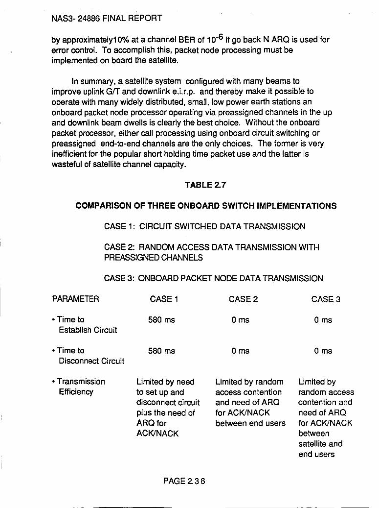
NAS3- 24886 FINAL REPORT
by approximately10% at a channel BER of 10 -6 if go back N ARQ is used for
error control. To accomplish this, packet node processing must be
implemented on board the satellite.
In summary, a satellite system configured with many beams to
improve uplink G/T and downlink e.i.r.p, and thereby make it possible to
operate with many widely distributed, small, low power earth stations an
onboard packet node processor operating via preassigned channels in the up
and downlink beam dwells is clearly the best choice. Without the onboard
packet processor, either call processing using onboard circuit switching or
preassigned end-to-end channels are the only choices. The former is very
inefficient for the popular short holding time packet use and the latter is
wasteful of satellite channel capacity.
TABLE 2.7
COMPARISON OF THREE ONBOARD SWITCH IMPLEMENTATIONS
CASE 1: CIRCUIT SWITCHED DATA TRANSMISSION
CASE 2: RANDOM ACCESS DATA TRANSMISSION WITH
PREASSIGNED CHANNELS
CASE 3: ONBOARD PACKET NODE DATA TRANSMISSION
PARAMETER CASE 1 CASE 2 CASE 3
• Time to
Establish Circuit
580 ms 0 ms 0 ms
• Time to
Disconnect Circuit
580 ms 0 ms 0 ms
• Transmission
Efficiency
Limited by need
to set up anddisconnect circuit
plus the need of
ARQ for
ACK/NACK
Limited by randomaccess contention
and need of ARQ
for ACK/NACK
between end users
Limited byrandom access
contention and
need of ARQ
for ACK/NACK
between
satellite and
end users
PAG E 2.3 6
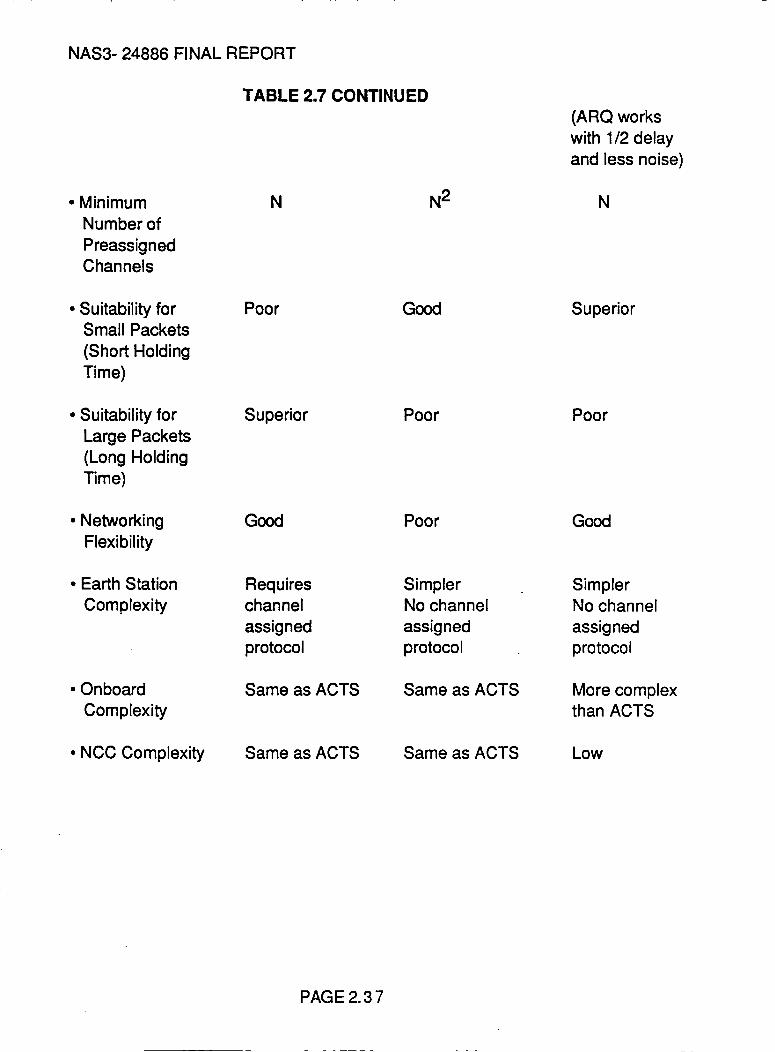
NAS3- 24886 FINAL REPORT
TABLE 2.7 CONTINUED
• Minimum
Number of
Preassigned
Channels
• Suitability for
Small Packets
(Short Holding
Time)
• Suitability for
Large Packets
(Long Holding
Time)
•Networking
Flexibility
• Earth Station
Complexity
• Onboard
Complexity
• NCC Complexity
N
Poor
Superior
Good
Requireschannel
assigned
protocol
Same as ACTS
Same as ACTS
N2
Good
Poor
Poor
SimplerNo channel
assigned
protocol
Same as ACTS
Same as ACTS
(ARQ works
with 1/2 delay
and less noise)
N
Superior
Poor
Good
SimplerNo channel
assigned
protocol
More complex
than ACTS
Low
PAGE 2.3 7
NAS3-24886 FINAL REPORT
2.6 ADVANCED SATELLITE TELECOMMUNICATIONS OPTIONS
Using the ACTS as a baseline, it is currently implemented as a circuit
switch in orbit in which the instructions controlling the interconnections
from channels in the uplinks to channels in the downlinks are stored in an
onboard program control memory but are changed in response to call
requests processed in a network control center (NCC) in the master control
station (MCS) located on the ground. Call request information is first
intercepted at an originating earth station and the request sent to the the
MCS via a satellite orderwire link. Using the current status of network
connectivities underway and the ensemble of requests from all stations,
the network control processor of the MCS generates new burst time plans
for all stations of the network, new switch commands for the onboard
connectivities between up and downlink channels and new beam dwell
patterns. These are distributed to the network via an orderwire link to the
earth stations and an orderwire link to the satellite. A coordinated time
plan change in which the the traffic stations invoke their new time plan
changes so that the changes are precisely synchronized at the satellite
with the onboard switch connection and beam dwell changes can be made
once every 300 ms.
In this advanced onboard processing and network control study, two
options are considered. The NCC and its call processing function could be
located onboard. This would reduce the amount of uplink communications
for switch control since the onboard switch is "smarter" and generates its
own switching instructions. Another option is to incorporate destination
directed packet switching in which each transmission burst has a
destination address in its header that is used onboard to direct the
message contents to the destination. These two configurations are
discussed in the following and the later has been selected for more
extensive examination in section 3 of this report.
In addition, the following text discusses of two ancillary issues that
are important to the future satellite system architecture, namely,
minimizing the size of the onboard storage by using to as great an extent
as possible the idea of "storage in space" and the integration of other
services and in particular mobile satellite communications.
2.6.1 ADVANCED NETWORK CONTROL
2.6.1.1 Call Processing On Board The Satellite
PAGE 2.3 8
NAS3-24886 FINAL REPORT
The possibility of locating the Network Control Center (NCC) and its
call processing function on board the satellite was analyzed. In this case
the signalling information is detected in the ground station and sent over
an order wire to the satellite where it is used to perform the same NCC
functions presently performed on the ground. This requires that the
satellite disseminate the new traffic burst time plans to all of the
affected traffic stations as well as determining and executing the onboardswitch connectivities and beam dwells.
An onboard NCC circuit switched alternative is made possible by
introducting common channel signaling. In common channel signalling the
signalling message is divorced from the channels with which it is
associated and the messages for all channels are sent over a common
channel. This is type of signalling that is being implemented in CCITT
signalling system No. 7. It could be sent directly to the satellite from a
single earth station and used for onboard NCC. Onboard the satellite it
would be used in the same way as signalling detected at the groundstations and sent to the satellite via the orderwire.
The principal advantage of locating the NCC function on the satellitewould be a reduction in the transmission load on the control link to the
satellite. An investigation to estimate the level of the reduction was made
and concluded that the savings would not be very great even for a
relatively large number of hopping beams (up to 10) and would likely not
justify the increased complexity, weight and power on the satellite. The
details are included as Appendix I and an associated Appendix 2.
2.6.1.2 Destination Directed On Board Switching
There exists the possibility that the voice circuits set up over the
system be virtual circuits similar to those used for data packets. This
could be accomplished by attaching to each burst of voice signal
information a destination port address in the system. An earth terminal
operating in this way would not be concerned about the specific location
of a channel in its frame since the destination address renders this
unnecessary. All the station needs is sufficient time slots in the TDMA
frame to handle its total traffic load. Voice signal bursts would be sent
only when the voice signal is actually present and thus the system would
in addition realize a speech interpolation activity advantage. Similarly,
there would be a data activity advantage. When these destination
addressed bursts are received onboard, they will be decoded and used to
direct the bursts to their proper destination port by assigning the bursts
to a downlink TDMA burst in the beam dwell containing the destination
PAGE 2.3 9

NAS3-24886 FINAL REPORT
station. Call setup would be conducted by similar destination directed
bursts. This concept could significantly simplify the network control
protocol in the area of dynamic assignment of individual channels in the
traffic burst time plans.
Because of the great promise of the destination directed message
approach, a large fraction of the effort expended under this study has been
devoted to the implementation of such a system. It is closely related to
the concept known as fast packet switching that is currently receiving
attention in all forms of voice data and teleconference communications.
Section 3 of this report deals exclusively with this approach. This study
considers the use of virtual circuits set up by destination addressing with
a virtual switching node located on board the satellite, identifies the
onboard implementation requirements, defines the features in the earth
station needed to operate with such a network and develops a protocol for
capacity and beam dwell adjustment among the stations.
2.6.2 MEMORY IN SPACE
Onboard Memory is essential to implementing an onboard switch.
Without it, it is not possible to redistribute the channels grouped
contiguously according to origin station arriving in uplink bursts into
downlink bursts grouped contiguously according to destination station. The
ability to reroute individual channels is the feature that distinguishes the
ACTS system from systems without memory such as SS-TDMA operating
with a MSM. As described previously, it greatly reduces the number of
individual traffic bursts and of beam hopping dwells.
The ACTS as it is presently designed uses separate input and output
memories, each comprising a pair of memories operating in a ping-pong
manner. At the input (uplink) one member of the pair stores the arriving
uplink channels while the other plays back the uplink channels stored on
the previous frame into a space switch that interconnects the beams. Theroles of the memories reverse from frame to frame an action referred to
as ping-pong. At the output (downlink) a pair of ping-pong memories
operate in a similar manner to accept the output channels from the space
switch and format these into the downlink groupings. This arrangement
requires a memory having a total size equal to four times the size of a
TDMA frame. The size of the memory can be decreased by a strategy
described in the following which uses the fact that the next channels to be
switched are stored in space and this storage can be used as part of the
switching operation.
PAGE 2.4 0
NAS3-24886 FINAL REPORT
By recognizing that the next channels to be switched reside in thespace immediately lying in front of the antenna and by designing thememory control to use this fact to advantage, the operations of storageand rearrangement into the desired downlink groupings can be performed ina memory having the capacity if a single frame. For destination packet likeswitching this design requires that the destination directing informationbe transmitted in the header of a burst arriving one frame before the burstcontaining the message to be switched. It also requires that the memorybe operated so that a channel just arriving occupy the location of thechannel that just departed on the downlink. This basic concept is used inthe design of the destination directed packet switch on board systemdescribed in Section 3 of this report.
2.6.3 INTEGRATING IN OTHER SERVICES
2.6.3.1 Capability to Accommodate Different Services
Future satellite communications payloads may be required to serve a
multiplicity of different communications services integrated into the
same package. This multiple service capability is greatly aided by the
presence of onboard demodulation of the uplink signals, channel level
switching and its associated storage and remodulation on the downlink.
The reason for this is that the signals onboard are reduced to the common
digital baseband denominator and can all be treated in a similar manner.
The differences lie in the demodulators and modulators that must render
the signals to the form that is needed to accommodate the type of service.
Probably the most different combination of services that can be
imagined would be the marriage of continuous SCPC digital mobile
services operating in a wide area coverage beam with the destination
directed burst telephone services operating in- a hopping spot beam
environment. From the point of view the type of service rendered and the
ground station equipment and protocols needed, these are widely different.
Thus in section 4, the integration of SCPC mobile services into
destination directed burst telephone services is used to demonstrate howa future satellite would accomodate different services. This is
sufficiently representative to allow for the extension to integrating manyother services.
2.6.3.2 Synchronization Among Different Services
k
One of the principle keys to integrating various services is
PAGE 2.41
NAS3-24886 FINAL REPORT
synchronization to a common timing base onboard the satellite. In TDMAsystems, this is accomplished as a consequence of the synchronizationdiscipline that is inherent in the acquisition and synchronization process.As long as all of the uplink signals are controlled by the same discipline itis possible to keep the individual bits that comprise the channelinformation properly aligned relative to the onboard clock with at most asmall alignment buffer to accommodate small timing variations. Thus, thecombination of different types of TDMA service in a common onboardprocessor even though each may use a different transmission burst ratedoes not pose a problem. This includes transmission over intersatellitelinks which can be viewed as simply the interface of another antennabeam.
This synchronization requirement does pose a problem that needs to
be resolved when it comes to continuous SCPC transmission signals. Such
transmissions are normally free from frame synchronization requirements
because they are unframed. However, in an onboard system that has a
frame structure discipline, it is necessary to establish one. To do this it
will be necessary to insert into the SCPC transmission a framing
discipline that can be used on the satellite to align the signals with thosederived from the other services.
With regard to downlink transmissions, the situation is not as
complicated as on the uplink. This is because all signals are time aligned
to the onboard timing and are inherently in a synchronous format that
easily accommodates reformating into various down link transmission
schemes to meet the needs of various types of service. The onboard
processing will in all likelihood treat all signals the same regardless of
their service origin. Thus, those channels associated with each type of
service can be supplied to the appropriate downlink interfaces equipped
with buffers to perform rate conversion. The downlinks may be high speed
TDM/TDMA carriers that are beam hopped to various destinations in which
case a burst forming buffer performing rate upconversion is needed. If the
the downlink rate happens to coincide with the rate used in the onboard
processor, the switching memory may serve as the burst forming buffer. If
the downlinks appear as continuous SCPC signals then a rate conversion
buffer that converts the onboard processor's channel bursts intocontinuous transmissions are needed.
2.6.3.3 Source Coding Considerations
There is one more issue that needs consideration when mixed services
PAGE 2.4 2
NAS3-24886 FINAL REPORT
are concerned and that relates to the method of source coding used. It
would be most desirable if all services used the same source coding
method. If this were so, no matter the nature of origin or destination of
the service it would always be in a compatible format. However, this may
not always be possible. For example, mobile services might well use a
heavily coded 4800 bit/s vocoder format to combat the vagaries of the
mobile transmission link and operate from small low powered earth
terminals while the trunk telephone services are likely to use one of the
source coders designed for toll quality service such as 64 kb/s PCM or 32
kb/s ADPCM. One solution to accommodate this difference is to include
onboard transcoders that convert the low bit rate formats to the standard
toll telephone format. An alternative is to carry the coded low bit rate
mobile service vocoder signals back to the earth terminals serving the
telephone service and perform the conversion there.
PAGE 2.4 3
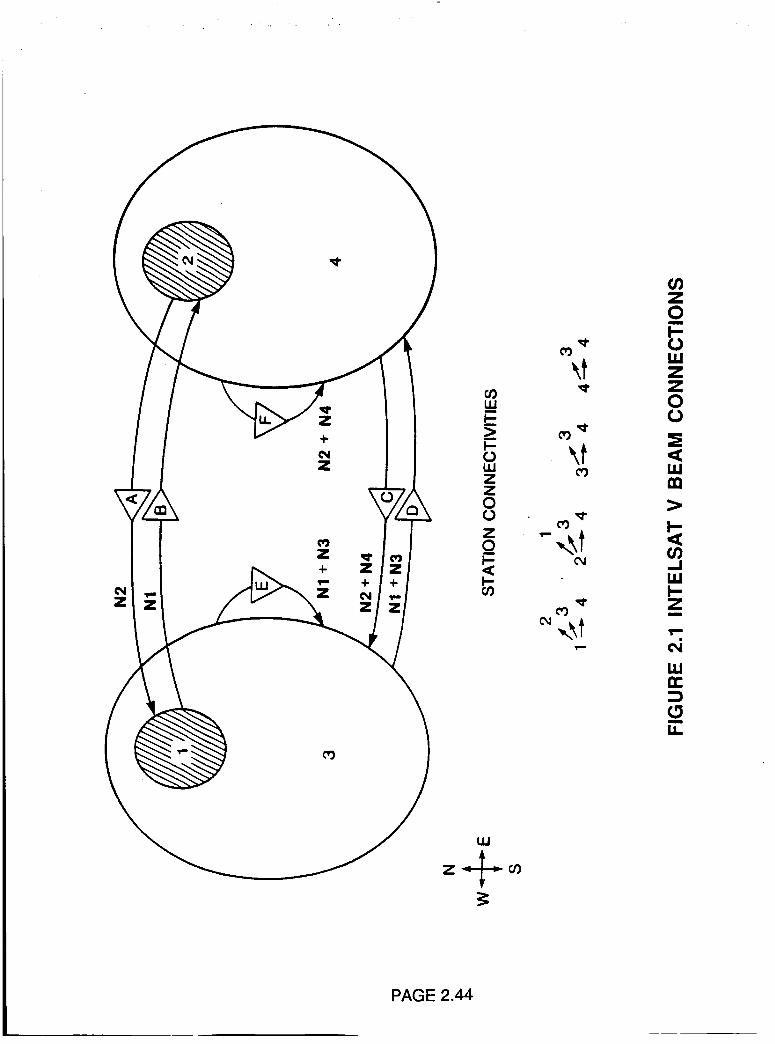
ZOm
I--OLI,,IZZ00
LU
)==
--/LUI.==Z
_q
IJa
I.i.
PAGE 2.44
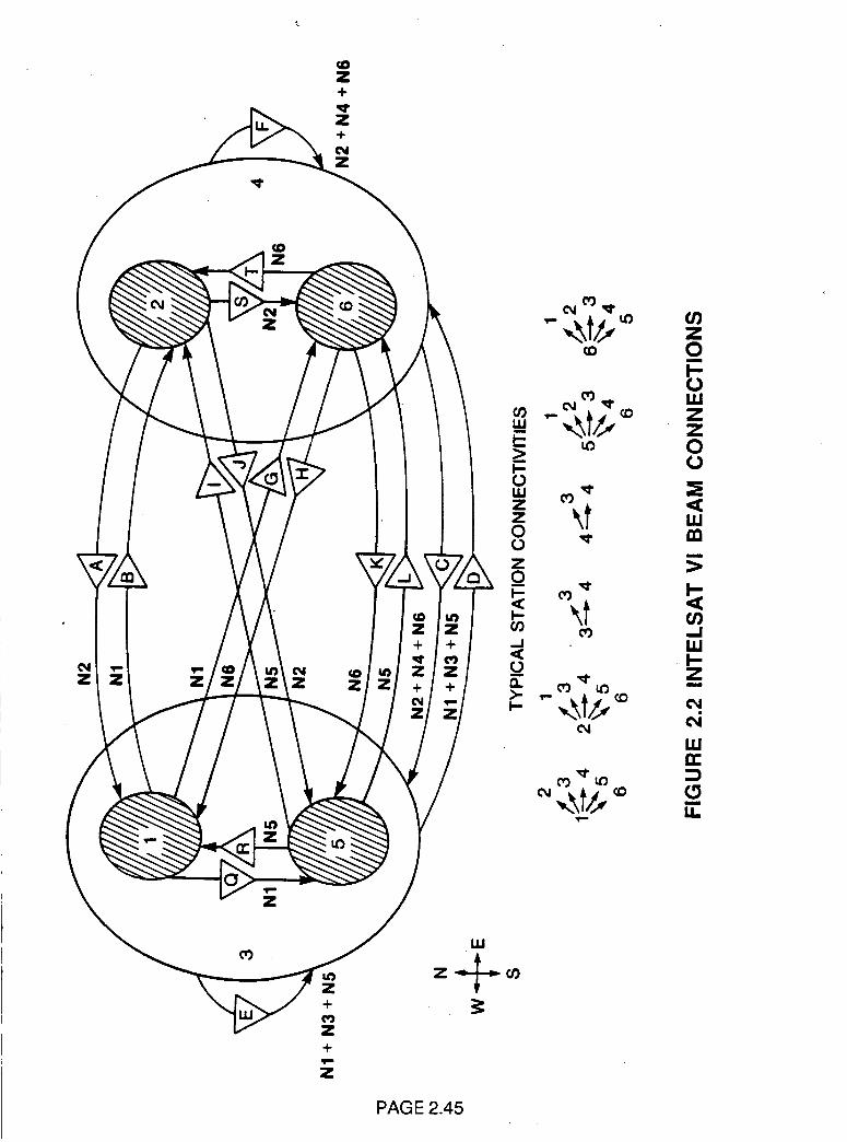
\/
+qlm
z
UJ
(/)Z0iii
I-014JzZ0(3
=i
LIJ00
m
>
I-
(/)..ILIJI--zi
c_
LIJ
0I.I.
PAG E 2.45
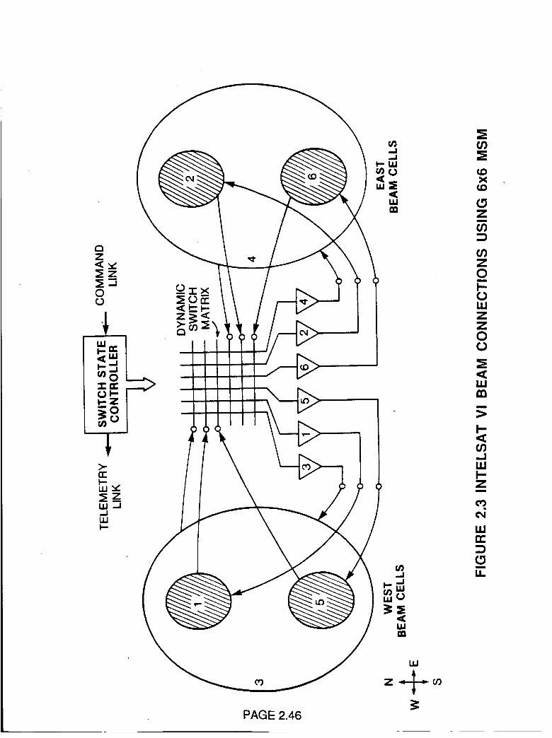
OCl-w__zw..JJWI-
PAGE 2.46
...di..,,,1,1,.I
I,i.I
3_
I.I,I
W
c_X
zm
mz0I-.
LUZZ0
LUm
I-,
m..ILUI--z
cO
LUrf"
LI.
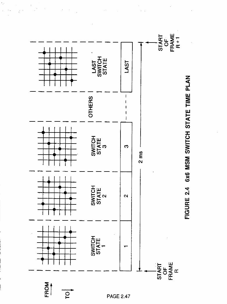
m ! ! _ m _ _ m m m ! _ q
II i =,,,Tl _°_-_ -- I--• IT "_ '
li
¢I) I
LUZ #I-- I0
I
ikIv
_)_
I
,w,
__)I.U
"I"u.I
Im._,__
m _ m _ m m A n .m w
t")
C_l
m
Im
PAGE 2.47
Ee_
i_ LIJ
-.---__=o_ _:
n
W
m
k-
I--
I'--
-r
I'--
lID
CID
ILl
m
IL
-I-. W
J-.__:.__ =<=
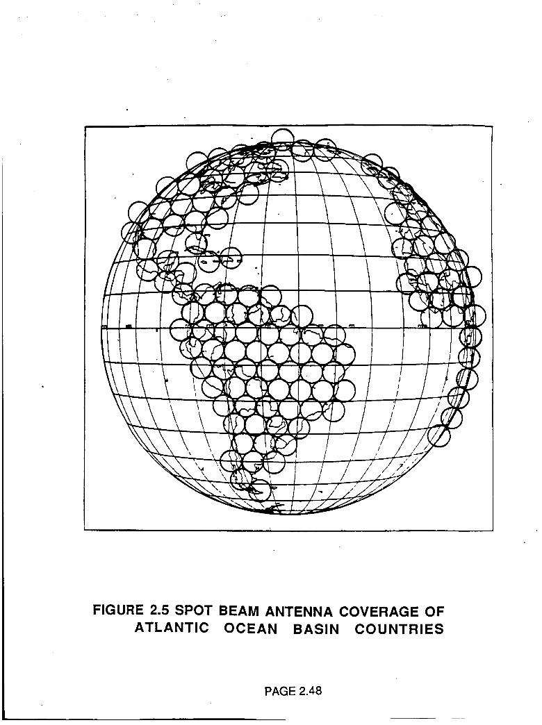
\\ /
/
/
III
//
/
FIGURE 2.5 SPOT BEAM ANTENNA COVERAGE OF
ATLANTIC OCEAN BASIN COUNTRIES
PAGE 2.48
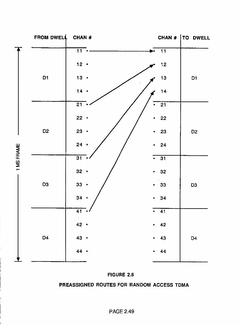
UJ
<ri-LL
u m
FROM DWELl
D1
CHAN # CHAN #
11 "=- 11
12 12
13 13
14 14
!TO DWELL
D1
22 •
D2
D3
D4
23 °
24 •
31 •
32 °
33 °
34 •
• 22
41 • • 41
42 • • 42
43 • • 43
23 D2
24
31
32
33 D3
34
D4
44 • • 44
FIGURE 2.6
PREASSIGNED ROUTES FOR RANDOM ACCESS TDMA
PAGE 2.49
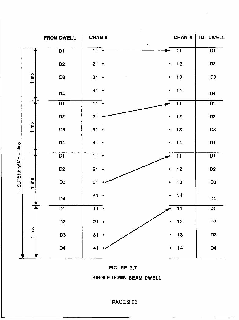
E
1
m
d
E
LL:n"LLIQ. ¢nD E
1"-"
o_E
_v
FROM DWELL
D1
D2
D3
D4
D1
D2
D3
D4
D1
D2
D3
D4
D1
D2
D3
D4
CHAN # CHAN #
11 • _"-- 11
21 • • 12
31 • • 13
41 • • 14
11 _ 1121 12
31 • • 13
41 • • 14
21 12
31 13
41 • • 14
11 11
21 • • 12
31 • • 13
41 • 14
TO DWELL
D1
D2
D3
D4
D1
D2
D3
D4
D1
D2
D3
D4
D1
D2
D3
D4
FIGURE 2.7
SINGLE DOWN BEAM DWELL
PAGE 2.50
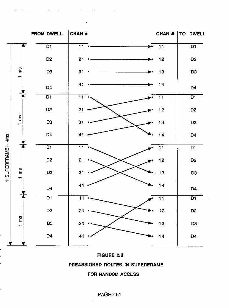
"t'-
_rE
(/}E
FROM DWELL
D1
D2
D3
D4
CHAN # CHAN #
11 • _'-- 11
21 • _- 12
31 • _: 13
41 • -'_ 14
TO DWELL
D1
D2
D3
D4
D1
D2
D3
D4
D1
D2
D3
D4
D1
D2
D3
D4
11 11
21 12
31 13
41 14
11 11
21 12
31 13
41 14
33 iT
21 12
31 13
41 14
D1
D2
D3
D4
D1
D2
D3
D4
D1
D2
D3
D4
FIGURE 2.8
PREASSIGNED ROUTES IN SUPERFRAME
FOR RANDOM ACCESS
PAGE 2.51
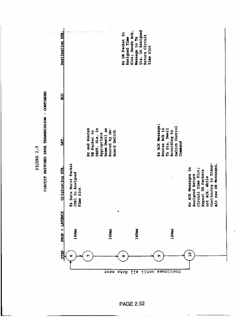
f.z,.
_J• '_ _0
>
_P
m i io c3 c3
E_ ..,-4
_._ _
PAGE 2.52
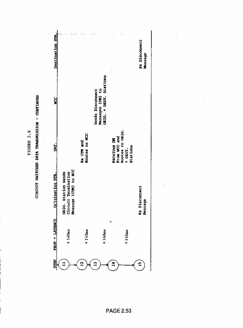
I
I,.-I
I,.,.I
)
r_
_o
r_m
_.,_®_Z
g" O
8®
r_
r'.0
mu_
_4
_1 ÷ ÷ ÷ ÷
PAGE 2.53
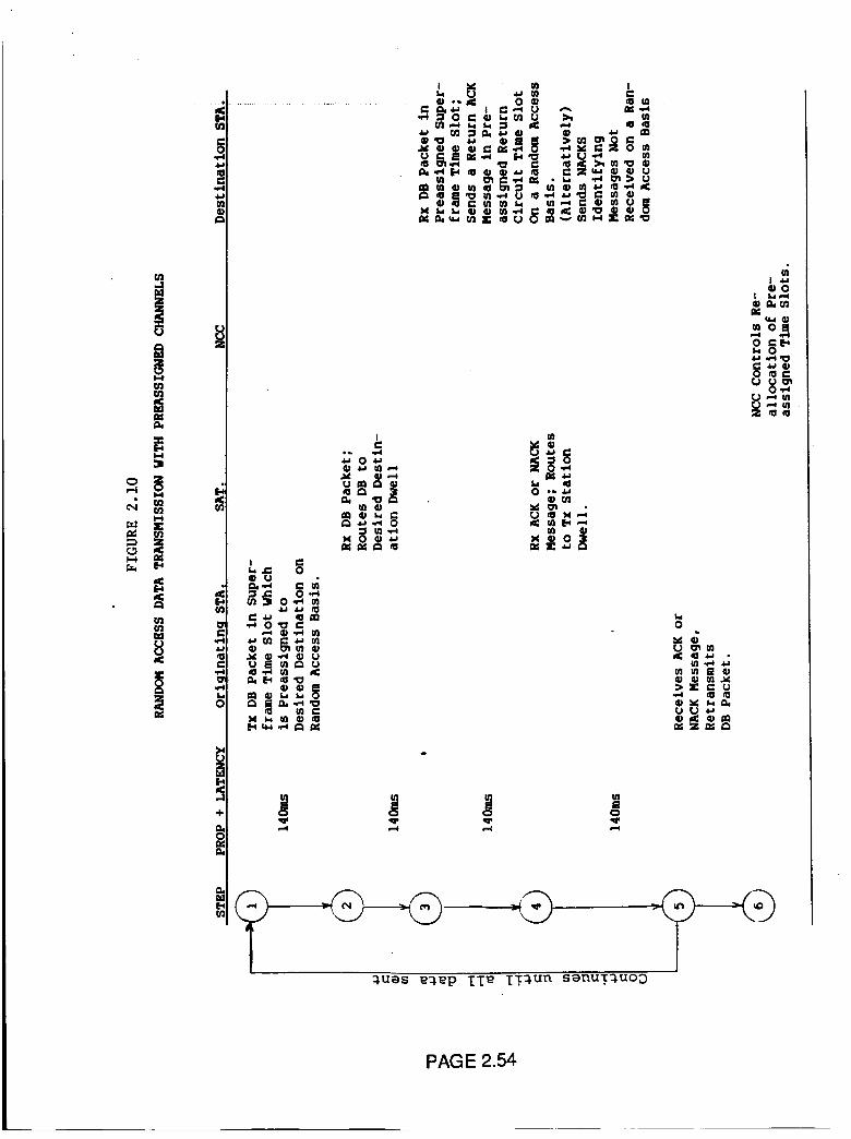
rj2r,_
0=
i-i
or,_i-4
M
J
Ic.,,_• U
U f
÷
I
I_ae
UU
'0 r'_ _.__I_ _) r./_
c,,,0 ,- a,,,_,
0 0 0
_ues e_p II_ IT_ un senuT_uoD
_0
_U3
_OE_
8 _
0
4.1
PAGE 2.54
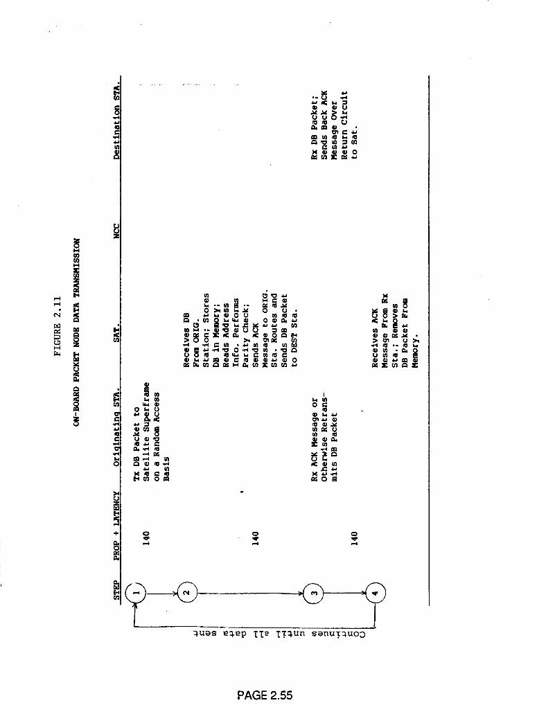
o.u
aJ
4- 0
4,J
U U
,,., _,_'_ ® ._,
Is_ _3o
E m
r_ s_
0 0
_ues _p II_ IT_Un senuT_uo3
PAGE 2.55
NAS3-24886 FINAL REPORT
3. DESTINATION DIRECTED PACKET ON BOARD PROCESSING ARCHITECTURE
Two different onboard switching architectures have been identified,
one using destination packet routing and the other using destination
directed sub-burst routing. The destination directed packet approach
encases each message in its own individual packet, each with its own
destination address, while the destination directed sub-burst approach
groups packets going to the same destination in a single sub-burst with
one destination address for the group. Tlie sub-burst approach provides
increased efficiency in terms of TDMA frame utilization whenever more
than one message is destined for a given destination. Increased frame
efficiency permits the use of a shorter TDMA frame duration which
reduces the size of the on board memory. This approach does however
slightly increase the complexity of the earth station equipment since
packets must be grouped according to their destinations before
transmission. Conversely however, the onboard processor design will be
slightly less complex since the packets arrive at the satellite grouped by
destination instead of in a completely arbitrary fashion. Both
architectures are described in greater detail in the following sections.
3.1 SYSTEM DESIGN
A description follows of a demand assignment satellite system that
uses destination directed message packets with an onboard°processing
satellite in the manner described above. The system comprises
terrestrial interfaces, earth stations, and the onboard processing
satellite as illustrated in figure 3.1.
3.1.1 DEMAND ASSIGNMENT OF CAPACITY
Capacity is allocated by the onboard processor in response to demands
of the earth stations. Circuits are assigned independently by each earth
station processor within its current capacity allocation as established by
the onboard network controller. Whenever the incoming demand on the
terrestrial ports at a given earth station exceeds that of the current burst
boundary (traffic burst boundaries), a request can be made directly to the
onboard processor to inCrease its allocation. Alternatively, the onboard
baseband processor will automatically adjust the capacity allocation by
knowledge of the number of channels currently active at each earthstation in the network.
If spare capacity exists, a reallocation will be made to a station
PAGE 3.1
NAS3-24886 FINAL REPORT
requiring additional capacity. If spare capacity does not exist, then the
call will be blocked by busying out the terrestrial circuit of the calling
party. Two examples of capacity reallocation are illustrated in figure 3.2.
The time interval shown corresponds to the uplink frame which is
subdivided into a number of uplink beam dwells. The first example shows
the case when two bursts exchange capacity while the others remain
unchanged. Note that this operation does not involve changing any of the
beam dwell boundaries. The second example shows the case when all
bursts change capacity. This does require changing the beam dwell
boundaries. As can be seen, capacity reallocation may involve reducing
the capacity of one or more bursts in the system which are not fully
utilizing their current allocation(s) to increase the capacity of other
bursts that have insufficient capacity.
3.1.1.1 Destination Addresses Packet Message
Within a given burst boundary allocation, terrestrial port to satellite
time slot allocations are made by each earth station processor for each
originating call. The uplink packet messages are mapped to the
appropriate downlink time slots by the onboard processor by the process
of reading the message packet header that contains the destination
address and assigning the packet message to an available downlink time
slot destined to the appropriate station. The packet messages are
assigned to available downlink time slots on a random occurrence basis (in
any order) only constrained by the current capacity allocation of thedestination station.
By this approach, the function of the onboard processor is that of
mapping uplink channels (time slots) into available downlink channels on a
frame by frame basis under the control of the destination address
information. In addition, the onboard processor must either accept
requests directly from traffic stations or autonomously reassign capacity
among the stations based on the current usage of satellite time slots. This
process may be viewed as a simplified burst time plan change which
involves changes to burst position and duration. Burst time plan changes
are executed by synchronous burst time plan change procedures from on
board the satellite. All other call setup elements such as port number to
satellite time slot associations are carried out entirely by individualearth station control.
One consequence of using destination addressed message packet
format for voice communications is in its inherent ability to serve as a
digital speech interpolation (DSI) system. The incorporation of a speech
PAGE 3.2
NAS3-24886 FINAL REPORT
activity detector on each of the terrestrial ports enables packets to be
sent only during the periods when speech activity is on the circuit, thus
providing an effective DSI gain.
3.1.2 METHOD OF OPERATION
The steps involved in operating an onboard processing satellite that
uses destination directed message packets is shown in Table 3.1. The
basic operation of the system can be subdivided into three sets of
procedures, namely: 1) call set-up, 2) call in progress and 3) calltermination.
3.1.2.1 Call Set-up Procedure
The signalling information is decoded at each terrestrial port. When
an off-hook condition is sensed on any terrestrial port, a call set-up
message (CSM) is sent via any free satellite time slot. A destination
address header is added to the packet which identifies the destination
earth station and the originating terrestrial port and earth station. The
data packet is assigned under local earth station control to any available
time slot within the station's traffic burst capacity allocation.
The transmit time slot assignments can be considered as terrestrial
port to satellite channel mappings which are performed by the
transmitting earth station using destination addressed packet messages.
Message packets will normally be assigned and reassigned to maintain
channel loading of the lower numbered satellite channel time slots, i.e.
those located closest to the leading edge of the traffic burst. This
procedure is sometimes referred to as "herding" of the channels because
they are confined to the leading portion of the burst. This procedure can
simplify the burst boundary reallocation procedure especially for bursts
which will be reduced in duration (capacity).
When the satellite processor receives the CSM, it decodes the packet
header and routes the entire message to an available time slot destined to
the addressed earth station. The onboard processor maps uplink message
packets to downlink satellite channels as shown for the example given in
figure 3.3. The onboard processor is free to select any available downlink
time slot destined for the addressed station. Normally the processor will
assign new channels and reassign existing channels to the lower numbered
time slots to confine the channels toward the leading edge of the burst in
a similar manner to what is done for the uplink assignments which are
made at the earth stations. If downlink capacity is not available,
PAGE 3.3
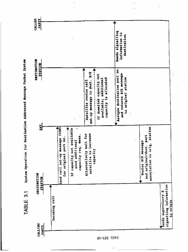
Elc_
r,n
.JJG
U
I:L
c_
M
:C
cnc_G
4:
GO
.IJm
.I.)W
o
o.,,.I
c_L
D,O
Mc_
W
cn
m
c:
..1
r_
ZOh-I
gB)-4i-,o2eL1
:RO
k,d
O
z
uV
®(;w_
WQI Id
E
WI G
4.) *_,,t
fA .g,t
O2
N O
,-4 • W
w w ,_ o w
'_, *.J_-) oW (_ -,-_ ,,-)
_J ao @ w
m
•,,,4 m
c_ _:o • c_
:_,_ >_
wcoI1t_
U
c_
ww o _
c4
o
c_
k, _1 c:o w o
o
w ,_ ,,.$
• Qw _G Q
0
o w
0 t,_ .
r _
_ n
I_.,_ +¢
"_ ._1
9_
&.r_-.f.,_S "t"_ 3
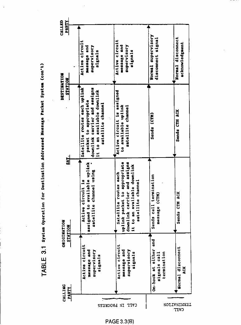
A
-=O
w>.trs_
mn.
G
mwm
QwwQL.
O
¢1
'4"0
w
r_C
C
L.@
O
E
W
_2
a
L_ i.qqO2 r._2_
.:1
lO
Z
I,-4
neO
ZO
l-,L
u (= i,__ q 0 m
¢j G .,.t al
• ..4 W _- W
U M W
k, 0 c_ :)--*
CD
.-* c.) _* 0
co 0 ,_
=.,w
IJ (11 (II
t.10 II
,,_ ¢11
• _i _/_
_ W _) ..,,,•_ _ _. CB
_ E W
•_ W D.W
_E W
C
W
m
_ &,, 0.-*
@ _1L,, ell .__.x c_ >..,*•_ _ ¢J ell _..*
._ ,x ._.* e8¢11 ¢= ,-* o _
Q M 0,,-*c_ cu
_ ¢_ _...,:) _ CD m
v
J_
w
w
m o
O
4k
O2
O
m
Jb
,C ,-_ 0
I
0
_J
0 E
I.I0 m
qP
q_
@
'qv
0
,<
NOI _YNIH_
TIV_
PAGE 3.3(B)
NAS3-24886 FINAL REPORT
additional capacity will be allocated by the onboard processor. This is
done by notifying via the reference burst all affected stations of the
changes to their burst position and duration. The onboard processor must
also adjust beam dwells in accordance with these changes in the burst
boundaries.
At the destination earth stations, an assignment is made of the
received CSM to an available terrestrial port. At the time of call setup,
normal signalling information is sent to the called party. In addition a
CSM ACK is sent back to the originating earth station giving the
association of the originating port to the destination port mapping.
For the case when satellite capacity is not available at the
originating earth station,either a capacity request message (CRM) is sent
over the order wire to the onboard processor to increase the station's
capacity allocation or if the onboard processor is equipped to perform
capacity reassignment by observing the number of channels that are active
at each earth station within the network, the station waits for more
capacity. Two allocation schemes are possible during the time lapse to
assign additional capacity. The first is to block the call and allocate
additional capacity for future voice calls. The other method is to queue
the call until the reallocation is made. The reallocation delay can probably
be kept to less than a few seconds and therefore the amount of memory
required and post dialing delay will be minimal. This approach can be used
both at the originating earth station for uplink satellite channels andonboard the satellite for downlink satellite channels.
Normal forward and backward signalling and supervisory signals are
sent to both the calling and the called parties.
3.1.2.2 Call In Progress Procedure
Upon completion of the call set-up procedure, the active circuit
message is sent over the circuit via destination addressed message
packets. Each message packet contains a header with a destination (or
origination) address and the call's destination (or origination) terrestrial
port number. This will be described in detail in section 3.1.2.4. As
described in the foregoing, the uplink satellite channel which is assigned
to carry a voice message packets changes from frame to frame as a
function of the happenstance of the activity on the voice ports. Also
message packets are assigned to the lowest numbered channels in order to
'herd' the active channels to the leading edge of the traffic burst. Each
downlink satellite circuit may also change from frame to frame under
control of the onboard processor for the same reason.
PAGE 3.4
NAS3-24886 FINAL REPORT
All message packets addressed to a particular destination address
will appear in their order of arrival on the incoming port assigned to the
call. When a message packet is not received due to a speech pause, an idle
signal will be sent on the terrestrial connection terminating that port.
3.1.2.3 Call Termination
When either party hangs up, an on-hook signal is detected at the
earth station which then initiates the transmission of a call termination
message (CTM) directed to the corresponding earth station. This message
is routed to the destination earth station by the onboard processor. The
corresponding earth station receives the CTM and signals the
corresponding party and also sends a CTM ACK to the corresponding earth
station. Both stations send the normal disconnect signals to the end
parties.
3.1.2.4 Mapping Functions
The entire DAMA/DSI system can be viewed as a three step mapping
operation as illustrated in figure 3.4. Terrestrial ports are mapped into
satellite time slots (channels) under independent earth station control by
assigning destination addressed message packets to the satellite channels.
These mappings can change on a frame by frame basis for.the following
reasons: 1) to maintain confinement of the channels to the leading portion
of the burst as calls terminate and 2) to assign active speech to available
channels on a random basis. Because of the packet header, no special
assignment channel is needed on the receive side to demap the channels.
On the transmit side, any active channel may be placed onto any available
satellite time slot. This process is viewed as the transmit terrestrial
port to satellite channel mapping. On the receive side, the received
message packets carried on the satellite channels are demapped using the
packet header which gives the destination terrestrial port number.
The third mapping function is performed onboard the satellite
where uplink satellite channels are mapped into available downlink
satellite channels. The only system constraint imposed on this mapping isthat the downlink channel selected is available and that it is directed to
the intended earth station, i.e. the one given in the packet header. This is
equivalent to requiring that the packet is placed onto the proper downlink
hopping beam dwell interval.
Figure 3.5 more precisely illustrates this three step mapping
procedure for the destination directed packet system:
PAGE 3.5
NAS3-24886 FINAL REPORT
1) the call originating station maps originating terrestrialports (TPos) into uplink satellite channels (SCUs),
2) the on-board processor maps the uplink satellite channelsinto downlink satellite channels (SCDs),
3) the call destination earth station maps downlink satellitechannels into destination terrestrial ports (TPds).
A packet comprises a header followed by a message. Figure 3.6 showsthe format of the packet header for a destination directed packet. Eachpacket header consists of a station I.D. number and a station terrestrialport number. Taking for example an 8 bit station I.D. and 8 bit stationport number, the header defines 256 station I.D.s and 256 station portnumbers. Another arrangement could be a 7 bit station I.D. and 9 bit portnumber to define 128 stations each serving 512 terrestrial ports. Takentogether, these 16 bits define 65,536 unique terrestrial port numbers. Aswill be seen later, the format of the packet header for the destinationdirected sub-burst approach only requires the station port number and istherefore more frame efficient.
3.1.2.5 Detailed Call Set-up Procedure
The signalling information is decoded at the originating station.When an off-hook condition is sensed at the originating station, aterrestrial port (TPo) is assigned and a call set-up message (CSM) is sent.A link must be established between TPo and a port at the destinationstation TPd via the onboard satellite switch. The TPo, TPd associationsform maps used to direct the calls. The procedure does not require storageof connectivity maps and their associated memory onboard the satellite.The procedure for doing this for both the destination directed packet(packet routing) and the destination directed sub-burst (sub-burst routing)approaches is described in Table 3.2 and Figures 3.7 and 3.8.
3.1.2.6 Detailed Call in Progress Procedure
Upon completion of the call set-up procedure, the active circuit voice
or data messages are sent over the circuit via the destination directed
message packets using the TPo, TPd associations established by either of
the two methods described in Table 3.2. The message portion of each
packet contains the active circuit voice or data message bits.
PAGE 3.6
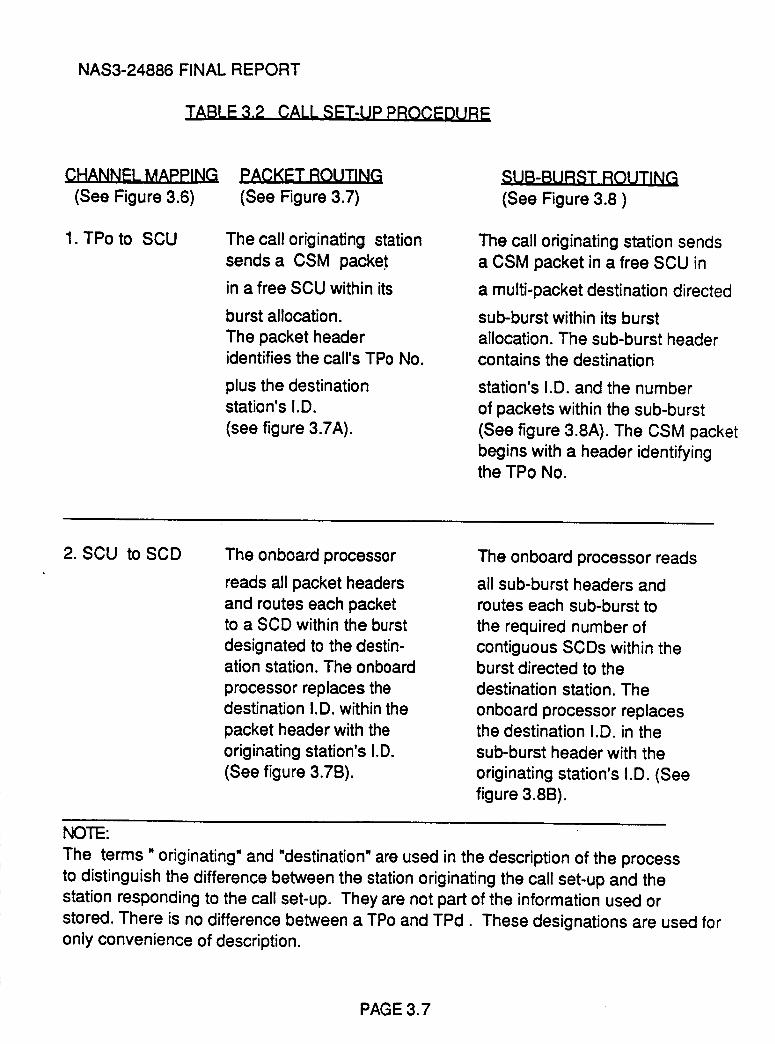
NAS3-24886 FINAL REPORT
TABLE 3.2 CALL SET-UP PROCEDURF
CHANNEL MAPPING
(See Figure 3.6)
1. TPo to SCU
PACKET ROUTING
(See Figure 3.7)
The call originating station
sends a CSM packet
in a free SCU within its
burst allocation.
The packet header
identifies the call's TPo No.
plus the destinationstation's I.D.
(see figure 3.7A).
SUB-BURST ROUTING
(See Figure 3.8 )
The call originating station sends
a CSM packet in a free SCU in
a multi-packet destination directed
sub-burst within its burst
allocation. The sub-burst header
contains the destination
station's I.D. and the number
of packets within the sub-burst
(See figure 3.8A). The CSM packet
begins with a header identifyingthe TPo No.
2. SCU to SCD The onboard processor
reads all packet headers
and routes each packetto a SCD within the burst
designated to the destin-ation station. The onboard
processor replaces thedestination I.D. within the
packet header with the
originating station's I.D.
(See figure 3.7B).
The onboard processor reads
all sub-burst headers and
routes each sub-burst to
the required number of
contiguous SCDs within theburst directed to the
destination station. The
onboard processor replacesthe destination I.D. in the
sub-burst header with the
originating station's I.D. (See
figure 3.8B).
NOTE:
The terms "originating" and "destination" are used in the description of the process
to distinguish the difference between the station originating the call set-up and the
station responding to the call set-up. They are not part of the information used or
stored. There is no difference between a TPo and TPd. These designations are used for
only convenience of description.
PAGE 3.7
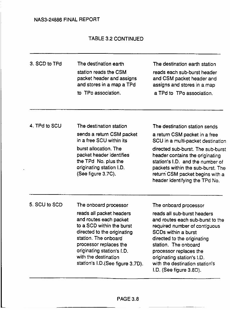
NAS3-24886 FINAL REPORT
TABLE 3.2 CONTINUED
3. SCD to TPd The destination earth
station reads the CSM
packet header and assigns
and stores in a map a TPd
to TPo association.
The destination earth station
reads each sub-burst header
and CSM packet header and
assigns and stores in a map
a TPd to TPo association.
4. TPd to SCU The destination station
sends a return CSM packetin a free SCU within its
burst allocation. The
packet header identifies
the TPd No. plus the
originating station I.D.
(See figure 3.7C).
The destination station sends
a return CSM packet in a free
SCU in a multi-packet destination
directed sub-burst. The sub-burst
header contains the originatingstation's I.D. and the number of
packets within the sub-burst. The
return CSM packet begins with a
header identifying the TPd No.
5. SCU to SCD The onboard processor
reads all packet headers
and routes each packetto a SCD within the burst
directed to the originatingstation. The onboard
processor replaces the
originating station's I.D.
with the destination
station's I.D.(See figure 3.7D).
The onboard processor
reads all sub-burst headers
and routes each sub-burst to the
required number of contiguousSCDs within a burst
directed to the originatingstation. The onboard
processor replaces the
originating station's I.D.
with the destination station's
I.D. (See figure 3.8D).
PAGE 3.8
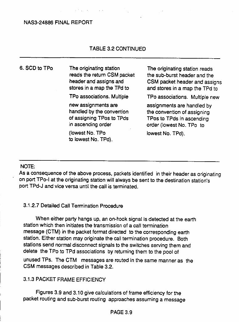
NAS3-24886 FINAL REPORT
TABLE 3.2 CONTINUED
6. SCD to TPo The originating station
reads the return CSM packet
header and assigns and
stores in a map the TPd to
TPo associations. Multiple
new assignments are
handled by the convention
of assigning TPos to TPds
in ascending order
(lowest No. TPo
to lowest No. TPd).
The originating station reads
the sub-burst header and the
CSM packet header and assigns
and stores in a map the TPd to
TPo associations. Multiple new
assignments are handled by
the convention of assigning
TPos to TPds in ascending
order (lowest No. TPo to
lowest No. TPd).
NOTE:
As a consequence of the above process, packets identified in their header as originating
on port TPo-I at the originating station will always be sent to the destination station'sport TPd-J and vice versa until the call is terminated.
3.1.2.7 Detailed Call Termination Procedure
When either party hangs up, an on-hook signal is detected at the earthstation which then initiates the transmission of a call termination
message (CTM) in the packet format directed to the corresponding earth
station. Either station may originate the call termination procedure. Both
stations send normal disconnect signals to the switches serving them and
delete the TPo to TPd associations by returning them to the pool of
unused TPs. The CTM messages are routed in the same manner as the
CSM messages described in Table 3.2.
3.1.3 PACKET FRAME EFFICIENCY
Figures 3.9 and 3.10 give calculations of frame efficiency for the
packet routing and sub-burst routing approaches assuming a message
PAGE 3.9
NAS3-24886 FINAL REPORT
channel transmission rate of 32 kbits/s. For the packet routing approach,
Figure 3.9 shows that to achieve a frame efficiency of about 94% (frame
efficiency loss of 6%) requires a frame period of about 16 ms. Figure 3.10
shows that the sub-burst routing approach provides approximately the
same frame efficiency with an 8 ms frame period. This represents
approximately a 50% reduction in the required frame period which will
translate into the same percentage of savings, i.e. 50%, in on-board
memory. These frame efficiency estlmates do not include the fraction of
the frame needed for TDMA reference bursts, network control bursts and
guard times.
3.1.4 DIGITAL SPEECH INTERPOLATION
As described above, if the system incorporates the use of digital
speech activity detectors at each terrestrial port, digital speech
interpolation (DSI) is automatically incorporated into system operation.
By sensing speech activity, message packets need only be transmitted
during periods of time when the circuit is active. This permits the
satellite channels to be shared among multiple voice conversations.
Normally, the DSI gain depends on the number of channels carried
by an earth station on a given link. The larger the link, the higher the gain.
For very thin route links, e.g., < 24 channels, the DSI gain may be
considerably less than 2.0. For this system however, the ensemble size is
not limited by the size of the link or the number of channels in a given
burst, but by the total capacity carried in a given beam dwell. This may be
composed of many links each carrying only a few channels. In a
conventional DSI system, the DSI gain would be low. However, if the burst
boundaries change to meet changes in instantaneous circuit demand, the
equivalent DSI gain will be higher since the total circuit ensemble will be
composed of the total channels within the beam dwell and not limited by
the number of channels on any given link.
3.1.5 ACQUISITION AND SYNCHRONIZATION CONTROL
The frame structure shown in figure 3.11 comprises the control and
traffic fields. In the downlink frame, the control field distributes
reference bursts to the traffic terminals, whereas in the uplink frame, the
control field provides request channels for acquiring traffic terminals.
The traffic field accommodates the traffic which is nominally one uplink
and one downlink burst per traffic terminal.
PAGE 3.1 0
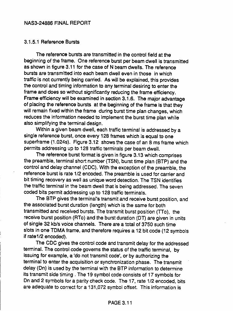
NAS3-24886 FINAL REPORT
3.1.5.1 Reference Bursts
The reference bursts are transmitted in the control field at the
beginning of the frame. One reference burst per beam dwell is transmitted
as shown in figure 3.11 for the case of N beam dwells. The reference
bursts are transmitted into each beam dwell even in those in which
traffic is not currently being carried. As wiJlbe explained, this provides
the control and timing information to any terminal desiring to enter the
frame and does so without significantly reducing the frame efficiency.
Frame efficiency will be examined in section 3.1.6. The major advantage
of placing the reference bursts at the beginning of the frame is that they
will remain fixed within the frame during burst time plan changes, which
reduces the information needed to implement the burst time plan while
also simplifying the terminal design.
Within a given beam dwell, each traffic terminal is addressed by a
single reference burst, once every 128 frames which is equal to onesuperframe (1.024s). Figure 3.12 shows the case of an 8 ms frame which
permits addressing up to 128 traffic terminals per beam dwell.
The reference burst format is given in figure 3.13 which comprises
the preamble, terminal short number (TSN), burst time plan (BTP) and the
control and delay channel (CDC). With the exception of the preamble, the
reference burst is rate 1/2 encoded. The preamble is used for carrier and
bit timing recovery as well as unique word detection. The TSN identifies
the traffic terminal in the beam dwell that is being addressed. The seven
coded bits permit addressing up to 128 traffic terminals.
The BTP gives the terminal's transmit and receive burst position, and
the associated burst duration (length) which is the same for both
transmitted and received bursts. The transmit burst position (TTo), the
receive burst position (RTo) and the burst duration (DT) are given in units
of single 32 kb/s voice channels. There are a total of 3750 such time
slots in one TDMA frame, and therefore requires a 12 bit code (12 symbolsif rate1/2 encoded).
The CDC gives the control code and transmit delay for the addressed
terminal. The control code governs the status of the traffic terminal, by
issuing for example, a 'do not transmit code', or by authorizing the
terminal to enter the acquisition or synchronization phase. The transmit
delay (Dn) is used by the terminal with the BTP information to determine
its transmit side timing. The 19 symbol code consists of 17 symbols for
Dn and 2 symbols for a parity check code. The 17, rate 1/2 encoded, bits
are adequate to correct for a 131,072 symbol offset. This information is
PAGE 3.11
NAS3-24886 FINAL REPORT
used by the terminal for performing both frame acquisition and
synchronization. For acquisition, the transmit delay is estimated by the
onboard processor from a knowledge of the satellite's position relative to
the acquiring traffic terminal. For synchronization, the value of transmit
delay is refined based upon the burst's observed time of arrival at the
satellite relative to the expected target position. Details of the
acquisition and synchronization procedures are given in section 3.1.5.3.
3.1.5.2 Uplink Request Bursts
The uplink control field provides uplink beam dwells as shown in
figure 3.11 which are coincident at the satellite with the downlink beam
dwells that are used for reference burst transmission. The uplink dwells
permit any station to request satellite access even those stations that are
located in a beam dwell region that is currently not carrying traffic. As
will be seen later, the uplink control field which is approximately equal in
duration to the downlink control field will not significantly reduce the
overall frame efficiency and therefore the beam dwells in the control
field can be permanently assigned. Any terminal requesting satellite
access will transmit a request burst (RQB) during its beam dwell and
within its allocated frame within the superframe.
The RQB shown in figure 3.14 consists of 13 contiguous sub-bursts
each of which comprise a carrier and bit timing (CTBR) sequence, unique
word (UW) and the burst number (BN). The RQB is transmitted by an
acquiring terminal in its allocated frame within the uplink superframe. As
in the case for the reference bursts, there is a ls superframe which
accommodates up to 128 traffic terminals per beam dwell. An acquiring
terminal will transmit in the time slot which corresponds to its terminal
short number.
The burst is sufficiently long (884 symbols) that at least one of the
13 sub-bursts will fall within a 136 symbol uplink dwell acquisition
aperture at the satellite. Since the sub-bursts are numbered, the onboard
processor can determine the amount that the RQB must be advanced or
retarded in time in order to move it to its nominal position within the
acquisition aperture. Details of the acquisition and synchronization
procedures follow in Section 3.1.5.3.
3.1.5.3 Acquisition and Synchronization Procedures
The process of terminal acquisition is performed using an open loop
approach which uses a knowledge of the satellite's position with respect
PAGE 3.1 2
NAS3-24886 FINAL REPORT
to the location of the acquiring terminal to compute its transmission
delay. It is assumed that the position of the satellite is known to better
than + 1.0 km from its actual postion. This corresponds to a maximum
uncertainty of about + 400 symbols or 800 symbols peak-to-peak. Since
the beam dwells can be arranged so that the RQB will not cause
interference into another beam dwell due to the spacial isolation of the
antenna beams, the RQB may be much longer than its allocated acquisition
beam dwell. In this system the RQB is chosen to be slightly greater than
the satellite's position uncertainty (800 symbols peak- to peak). In this
way, one RQB sub-burst will always be detected at the satellite within an
uplink dwell aperture. This aperture as shown in figure 3.15 is chosen to
equal 2 times the length of the sub-burst (136 symbols).
The unique word aperture is initially opened to a window width equal
to the sub-burst length plus one symbol or 69 (68+1) symbols. Upon
detection of the unique word, the aperture is reduced to a window width
that is equal to the unique word length and positioned at the instant of the
observed unique word detection. This step is performed to reduce the
probability of false unique word detection.
The uplink and downlink superframes are aligned at the satellite. To
transmit the request burst, the terminal receives the reference burst
directed to it and decodes the BTP and CDC. From this information, the
terminal can transmit its RQB. The control code will normally contain a
'request burst authorized' code together with the values of Dn and TTo
which will place the RQB in its proper acquisition slot. Upon proper
reception of the RQB, the reference burst will change the control code to
'acquisition authorized'. The reference burst will also send the TTo and
refined value of Dn which will permit the terminal to place its burst (less
traffic) into its nominal position in the traffic field. The onboard
processor must ensure that adequate capacity and beam dwell has been
allocated to this terminal. Upon reception of the acquisition burst in its
proper position in the traffic field, the reference burst will send the
"Synchronization Code" to the terminal with a limited amount of capacity
allocation (DT). If at any time the traffic burst moves outside of a
specified aperture, for example, by more than + 8 symbols, the reference
burst control code will change to "Do Not Transmit" which takes the
traffic terminal off the air.
3.1.6. OVERALL FRAME EFFICIENCY
The loss in frame efficiency caused by the presence of the control
field is governed by the uplink frame since the uplink dwell that is needed
PAGE 3.1 3
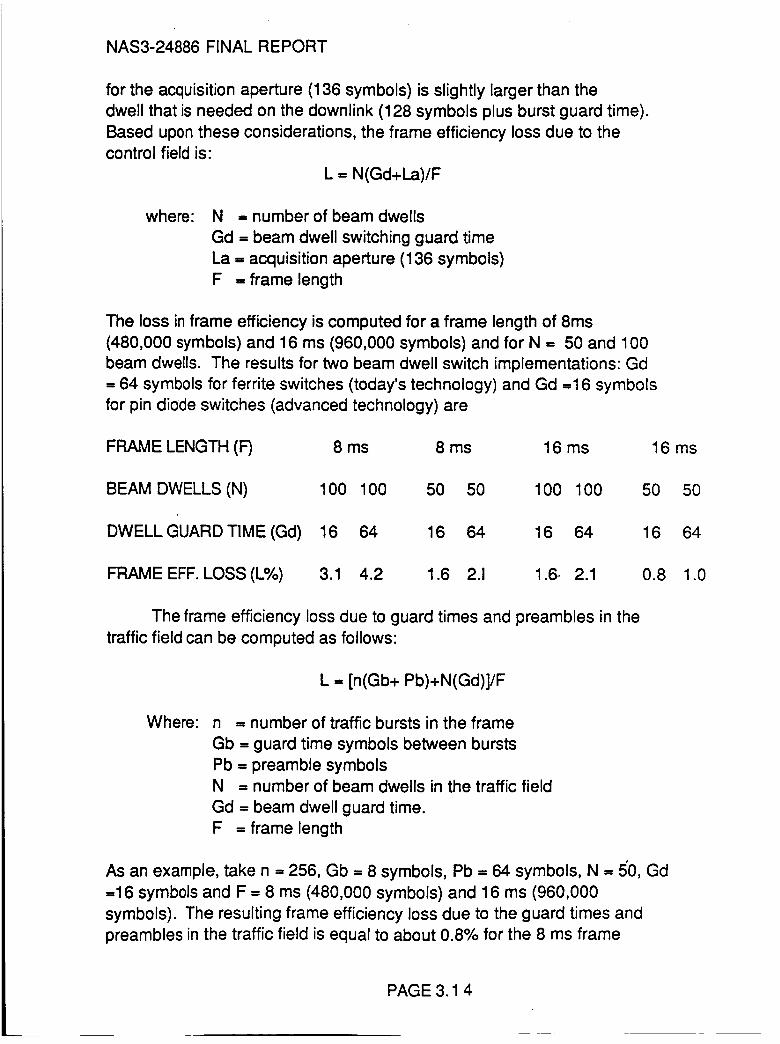
NAS3-24886 FINAL REPORT
for the acquisition aperture (136 symbols) is slightly larger than thedwell that is needed on the downlink (128 symbols plus burst guard time).Based upon these considerations, the frame efficiency loss due to thecontrol field is:
L = N(Gd+La)/F
where: N -- number of beam dwells
Gd = beam dwell switching guard time
La - acquisition aperture (136 symbols)
F = frame length
The loss in frame efficiency is computed for a frame length of 8ms
(480,000 symbols) and 16 ms (960,000 symbols) and for N = 50 and 100
beam dwells. The results for two beam dwell switch implementations: Gd
-- 64 symbols for ferrite switches (today's technology) and Gd --16 symbols
for pin diode switches (advanced technology) are
FRAME LENGTH (F) 8 ms 8 ms 16 ms 16 ms
BEAM DWELLS (N) 100 100 50 50 100 100 50 50
DWELL GUARD TIME(Gd) 16 64 16 64 16 64 16 64
FRAME EFF. LOSS (L%) 3.1 4.2 1.6 2.1 1.6 2.1 0.8 1.0
The frame efficiency loss due to guard times and preambles in the
traffic field can be computed as follows:
L = [n(Gb+ Pb)+N(Gd)]/F
Whe_: n = number of traffic bursts in the frame
Gb = guard time symbols between bursts
Pb = preamble symbols
N = number of beam dwells in the traffic field
Gd = beam dwell guard time.
F = frame length
As an example, take n = 256, Gb = 8 symbols, Pb = 64 symbols, N = 50, Gd
=16 symbols and F -- 8 ms (480,000 symbols) and 16 ms (960,000
symbols). The resulting frame efficiency loss due to the guard times and
preambles in the traffic field is equal to about 0.8% for the 8 ms frame
PAGE 3.1 4
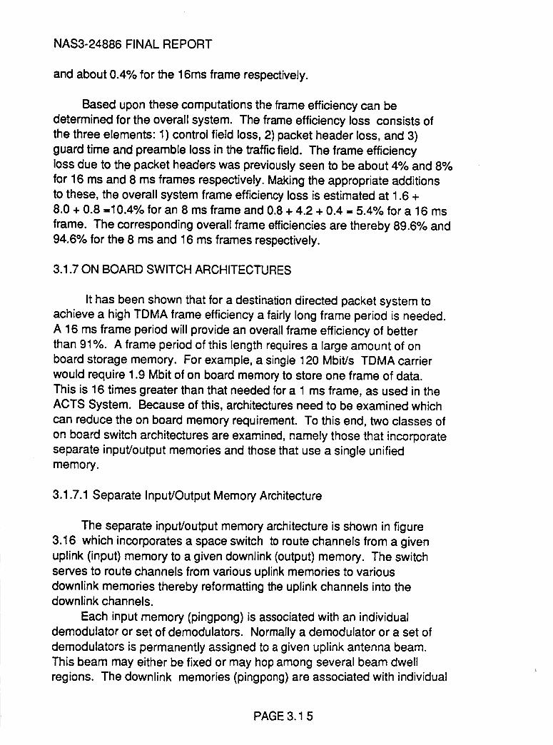
NAS3-24886 FINAL REPORT
and about 0.4% for the 16ms frame respectively.
Based upon these computations the frame efficiency can be
determined for the overall system. The frame efficiency loss consists of
the three elements: 1) control field loss, 2) packet header loss, and 3)
guard time and preamble loss in the traffic field. The frame efficiency
loss due to the packet headers was previously seen to be about 4% and 8%
for 16 ms and 8 ms frames respectively. Making the appropriate additions
to these, the overall system frame efficiency loss is estimated at 1.6 +
8.0 + 0.8 =10.4% for an 8 ms frame and 0.8 + 4.2 + 0.4 = 5.4% for a 16 ms
frame. The corresponding overall frame efficiencies are thereby 89.6% and
94.6% for the 8 ms and 16 ms frames respectively.
3.1.7 ON BOARD SWITCH ARCHITECTURES
It has been shown that for a destination directed packet system to
achieve a high TDMA frame efficiency a fairly long frame period is needed.
A 16 ms frame period will provide an overall frame efficiency of better
than 91%. A frame period of this length requires a large amount of on
board storage memory. For example, a single 120 Mbit/s TDMA carrier
would require 1.9 Mbit of on board memory to store one frame of data.
This is 16 times greater than that needed for a 1 ms frame, as used in the
ACTS System. Because of this, architectures need to be examined which
can reduce the on board memory requirement. To this end, two classes of
on board switch architectures are examined, namely those that incorporate
separate input/output memories and those that use a single unified
memory.
3.1.7.1 Separate Input/Output Memory Architecture
The separate input/output memory architecture is shown in figure
3.16 which incorporates a space switch to route channels from a given
uplink (input) memory to a given downlink (output) memory. The switch
serves to route channels from various uplink memories to various
downlink memories thereby reformatting the uplink channels into thedownlink channels.
Each input memory (pingpong) is associated with an individual
demodulator or set of demodulators. Normally a demodulator or a set of
demodulators is permanently assigned to a given uplink antenna beam.
This beam may either be fixed or may hop among several beam dwell
regions. The downlink memories (pingpong) are associated with individual
PAGE 3.1 5
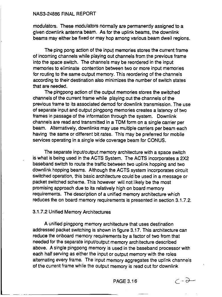
NAS3-24886 FINAL REPORT
modulators. These modulators normally are permanently assigned to a
given downlink antenna beam. As for the uplink beams, the downlink
beams may either be fixed or may hop among various beam dwell regions.
The ping pong action of the input memories stores the current frame
of incoming channels while playing out channels from the previous frame
into the space switch. The channels may be reordered in the input
memories to eliminate contention between two or more input memories
for routing to the same output memory. This reordering of the channels
according to their destination also minimizes the number of switch statesthat are needed.
The pingpong action of the output memories stores the switched
channels of the current frame while playing out the channels of the
previous frame to its associated demod for downlink transmission. The use
of separate input and output pingpong memories creates a latency of two
frames in passage of the information through the system. Downlink
channels are read and transmitted in a TDM form on a single carrier per
beam. Alternatively, downlinks may use multiple carriers per beam each
having the same or different bit rates. This may be preferred for mobile
services operating in a single wide coverage beam for CONUS.
The separate input/output memory architecture with a space switch
is what is being used in the ACTS System. The ACTS incorporates a 2X2
baseband switch to route the traffic between two uplink hopping and two
downlink hopping beams. Although the ACTS system incorporates circuit
switched operation, this basic architecture could be used in a message or
packet switched scheme. This however will not likely be the most
promising approach due to its relatively high on board memory
requirements. The description of a unified memory architecture which
reduces the on board memory requirements is presented in section 3.1.7.2.
3.1.7.2 Unified Memory Architectures
A unified pingpong memory architecture that uses destination
addressed packet switching is shown in figure 3.17. This architecture can
reduce the onboard memory requirements by a factor of two from that
needed for the separate input/output memory architecture described
above. A single pingpong memory is used in the baseband processor with
each half serving as either the input or output memory with the roles
alternating every frame. The input memory aggregates the uplink channels
of the current frame while the output memory is read out for downlink
PAGE 3.16 d__-
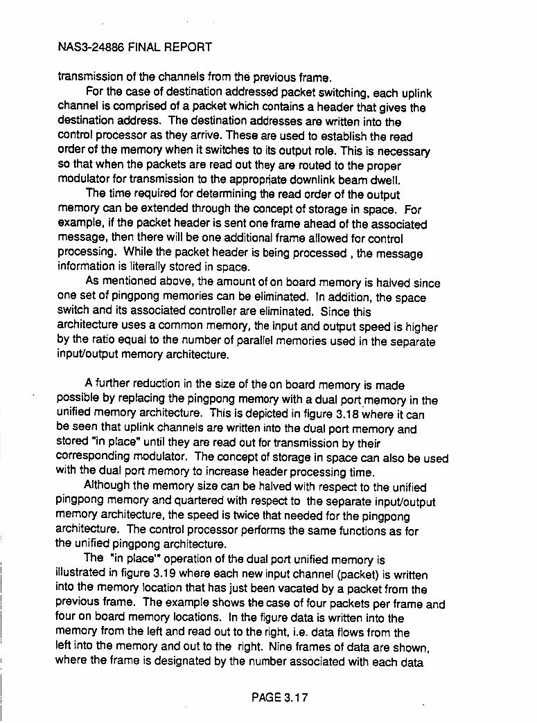
NAS3-24886 FINAL REPORT
transmission of the channels from the previous frame.
For the case of destination addressed packet switching, each uplink
channel is comprised of a packet which contains a header that gives thedestination address. The destination addresses are written into the
control processor as they arrive. These are used to establish the read
order of the memory when it switches to its output role. This is necessary
so that when the packets are read out they are routed to the proper
modulator for transmission to the appropr!ate downlink beam dwell.
The time required for determining the read order of the output
memory can be extended through the concept of storage in space. Forexample, if the packet header is sent one frame ahead of the associated
message, then there will be one additional frame allowed for control
processing. While the packet header is being processed, the messageinformation is literally stored in space.
As mentioned above, the amount of on board memory is halved since
one set of pingpong memories can be eliminated. In addition, the spaceswitch and its associated controller are eliminated. Since this
architecture uses a common memory, the input and output speed is higher
by the ratio equal to the number of parallel memories used in the separateinput/output memory architecture.
A further reduction in the size of the on board memory is made
possible by replacing the pingpong memory with a dual port memory in the
unified memory architecture. This is depicted in figure 3.18 Where it can
be seen that uplink channels are written into the dual port memory and
stored "in place" until they are read out for transmission by their
corresponding modulator. The concept of storage in space can also be used
with the dual port memory to increase header processing time.
Although the memory size can be halved with respect to the unified
pingpong memory and quartered with respect to the separate input/output
memory architecture, the speed is twice that needed for the pingpongarchitecture. The control processor performs the same functions as for
the unified pingpong architecture.
The "in place'" operation of the dual port unified memory is
illustrated in figure 3.19 where each new input channel (packet) is written
into the memory location that has just been vacated by a packet from the
previous frame. The example shows the case of four packets per frame and
four on board memory locations. In the figure data is written into the
memory from the left and read out to the right, i.e. data flows from the
left into the memory and out to the right. Nine frames of data are shown,
where the frame is designated by the number associated with each data
PAG E 3.1 7

NAS3-24886 FINAL REPORT
packet. At the top of the figure, the memory starts in the empty condition.
At this point, the first frame of data (A1 ,B1 ,C1 ,D1) is being stored in
space. In the second frame the data is stored in the on board memory. Data
is read out for the first time in the third frame. In this example, the data
is read out in the sequence of B,D,A,C, however it can be written out in any
sequence. Each new input packet is written into the memory location of
the just vacated memory location. Because of this process the packets can
be seen to be stored in any of the four memory locations, independent of
their origin or destination. The method of implementing this architecture
is given in section 3.2.
PAG E 3.1 8
NAS3-24886 FINAL REPORT
3.2 BASEBAND PROCESSOR IMPLEMENTATION
Section 2 of this report described the advantages and call processing
procedures of a destination-directed packet Switching approach. This was
expanded upon in section 3.1 where the protocols were defined for the
on-board switch architecture. This section .will describe three
specific destination-directed onboard switch architectures and present
block diagram level hardware implementations, showing the various
performance, chip-count, and power trade-offs for each. The first
architecture is similar to that of the ACTS, employing separate uplink and
downlink memories coupled by a space switch. The other two architectures
are based on a single, large "unified" memory utilizing storage in space.
3.2.1 SEPARATE INPUT/OUTPUT MEMORY ARCHITECTURE
Figure 3.20 shows the basic elements of the Separate Input/Output
Memory architecture. Three individual upbeams and downbeams are shown
although it could be expanded to many more. Individual demodulated
packets arriving on upbeams A, B, and C are buffered in their associated
input memory in their order of arrival. The input buffers must be large
enough to store an entire frame of packets. The packets are then routed to
the proper downbeam destinations through the 3 X 3 switch matrix. It will
be assumed throughout this section that each packet contains its own
destination address included in its packet header. The packets are buffered
in the appropriate downbeam output memories before being remodulated
and transmitted to the Earth. The memories could be either pingpong or
dual-port arrays. This will be discussed in the hardware implementationsection later.
Figure 3.20 represents the traditional time-space-time architecture as
used in the ACTS. One important difference, however, is that the packetsare message switched rather than circuit switched. Packets destined for
various downbeams may arrive in any order within a given TDMA burst and
do not have to be sent in any predefined sequence synchronized with the
satellite network. The on-board processor will reorder the packets after
they have been buffered in the input memories. The packets arriving in
Figure 3.20 are labelled according to their destination addresses. The
subscripts do not carry any significance except to illustrate the sequence
of packets flowing through the architecture. Each packet is stored in a
PAGE 3.19
NAS3-24886 FINAL REPORT
unique memory address. For example, input memory for upbeam A occupies
addresses 00 through 06. Each beam must have its own unique memory
since all beams function simultaneously.
Note that the input packets are stored in their order of arrival. The
packets must be reordered in coordination with the switch matrix so that
for each switch state the packets sent to switch ports 1,2, and 3 arrive at
the appropriate switch output ports 4, 5, and 6. For a 3 X 3 switch as
shown, there are a total of 29 ., 512 possible switch states. The
computational load in calculating the proper switch states in real time ( on
a frame by frame basis) for a given frame of destination-directed packets
would be enormous even for a simple 3 X 3 switch. As a result the switch
states must be precomputed on-board based on the anticipated traffic
between each pair of beams. This is a reasonable assumption for voice
traffic which is only slowly time variant. The only drawback to this
approach is that extra switch states must be included to make sure that
every arriving packet can be assigned to a valid switch state. The total
system capacity will be reduced by the amount of unused switch overhead.
In addition, calculating switch states at a very slow rate still requires a
complex processor and the switch would not easily adapt to rapidly
changing data traffic. The switching algorithm must be optimized to
simultaneously route valid packets to every downbeam for maximum
throughput.
The incoming packets are reordered by means of an input memory map.
Every input memory location has a corresponding control memory location,
as shown in Figure 3.21. There is a separate bank of control memory for
each upbeam A, B, and C. Each bank is partitioned into three groups
reserved for downbeams A, B, and C. A group's size is precomputed
according to the number of switch states reserved for that specific
upbeam-downbeam pair. Each time a packet is written to the input
memory, the input memory address is written to the next available location
in control memory in the group corresponding to the packet's destination.
For example, in Figure 3.20 the packets labelled A1 and C1 are written to
locations 00 and 01 of upbeam A input memory. The address 00 is written
to location 00 of upbeam A control memory (first location of group
reserved for downbeam A) and the address 01 is written to location 05 of
upbeam A control memory (first location of group reserved for destination
C). Each control memory group has a unique downbeam pointer as shown in
Figure 3.21. The group boundaries are determined by the initial values of
the pointers. Whenever input memory is written, the proper pointer is
PAGE 3.2 0
NAS3-24886 FINAL REPORT
selected according to the destination contained within a packet's header.
Input memory addressing has two levels of indirection as a pointer
addresses control memory which in turn addresses the input memory. The
pointers are post-incremented after an access to point to the next free
control memory address. Note that each group must contain extra locations
to avoid overflow. At the end of a frame, the values of the pointers will
give the statistics on traffic between each pair of beams. The on-board
processor can read the pointers to calculate the next frame's switchstates.
Once the control memory has been filled with an entire frame a second
set of pointers is initialized to the top of each group and the input memory
can be downloaded to the output memory through the switch matrix. The
switch states are sequenced through a precomputed set of states stored in
switch state memory. The switch states select the pointers to address the
packets with the desired downbeam destinations. The output memories are
simply loaded in sequence and do not require any special addressing
techniques. Similarly, the pointers are simply incremented in sequence
after each access. The table in Figure 3.21 shows the sequence of switch
states and the corresponding input memory addresses read from control
memory to load the output memory. Switch states I and IV are repeated 3
times due to a large amount of traffic anticipated between their associated
nodes. In both cases the switch states are only required twice and the
control memories must be disabled during the third occurrences. The first
occurrence of switch state I makes the following upbeam/downbeam
connections: NA, B/B, C/C. The pointers select control memory addresses
00, 12, 26 which select input memory locations 00, 10, and 23 respectively
and packets A1, B1, and C1 are put in output memory. Once the output
memory has been loaded, packets are transferred to the downbeams by
simply sequencing through the output memories in order. Additional logic
must be added to turn off a downbeam (or generate an idle bit pattern)
when the last valid output memory location has been read.
3.2.1.1 Separate Input/Output Memory Hardware Implementation
For purposes of comparison the following design example will be used
throughout the remainder of this report:
* 10 IDENTICAL UPBEAMS, 120 MBPS EACH
* 10 IDENTICAL DOWNBEAMS, 120 MBPS EACH
* FRAME LENGTH = 16 ms (SEE SECTION 3.1.3)
PAGE 3.21
NAS3-24886 FINAL REPORT
* FRAME SIZE - 10 X 120 MBPS X 16 ms - 19.2 MBITS* TOTAL NO. OF 1-WAY 32 KBPS VOICE CIRCUITS =
(19.2 MBITS/FRAME) / (544 BITS/PACKET) .- 35,000
(UP TO 70,000 WITH INHERENT DSI ADVANTAGE)
3.2.1.1.1 System Memory Requirements
Assuming a 2:1 DSl advantage, the example architecture would have a
voice circuit capacity slightly greater than 50% of the INTELSAT VI. Due to
the extremely long frame length, the driving force in this new architecture
is the size and power requirements of the on-board memory.
In the ACTS system the input and output memories are pingpong arrays
requiring two frames of storage per input or output memory. Packets from
the current frame are written into one half while packets from the
previous frame are read from the other half. Both halves reverse roles once
the current frame is complete. This approach allows both read and write
cycles to occur simultaneously. Another possible implementation would be
to use a single frame of dual ported memory. A dual ported memory hastwo sets of address and data busses to allow simultaneous read and write
cycles to different addresses. A dual ported RAM would be an effective
approach if it was at least half as dense as an equivalent single ported RAM
since only half the amount of storage is required. Today's dual ported RAM
devices are not an effective solution since their densities are typically 4
times less than the densest available single-ported RAM.
Another way to implement dual ported RAM is by using a single ported
RAM of twice the required speed and time-sharing the bus between read and
write cycles. In this approach, a full frame is buffered in the memory and
then every time a word is read, a new word is written over it in the same
location. This "in-place" approach was illustrated in Figure 3.19. The
control memories will have to be pingpong to keep track of the inputmemory read and write addresses. This turns out to be an excellent
trade-off since the control memory is much smaller than the input
memory.
As an example, suppose the input memories are loaded as shown in
Figure 3.20 and the control memories are loaded as shown in Figure 3.21.
On the next memory bus cycle the input memory will begin writing its
contents to the switch matrix. If A1 is written to the switch, then input
PAGE 3.22
NAS3-24886 FINAL REPORT
memory location 00 will be free. On the following memory bus cycle the
direction of the input memory busses will reverse. The next arriving
packet on upbeam A will then be written to input memory location 00. 00
will be written to either group A, B, or C of upbeam A control memory
depending on the packer's destination. Thus the control memories map the
'free' input memory locations as well as sort the incoming packets by
destination. Upon system initialization the on-board processor will fill
one side of the pingpong control memories with a unique set of addresses
to provide a complete map of free input memory locations.
For this 'in-place' method to work, the control memories must be
accessed every bus cycle whether a valid packet is accessed or not. This
allows the next 'free' input memory address to always be latched for the
next input memory write. Consequently, if a particular upbeam burst does
not occupy its entire allotted time, then the control memory will just cycle
through new addresses at the end of the burst without actually accessing
any packet data. The input memory must somehow be labelled to indicate
which input memory addresses contain empty packets. See Section3.2.1.1.1.4 for further details.
There are a total of four different memory storage subsystems for this
architecture: input/output memories, control memory, switch state
memory, and packet header memory. They are outlined in the followingsections.
3.2.1.1.1.1 Input/Output Memory Requirements
This section outlines the storage requirements for the input and output
memories. Both require equal amounts of storage. These 2 subsystems
store only the 512-bit data portion of a packet and not the header
information. The "in-place" technique is used.
The 120 Mbps serial data streams are much too fast for conventional
memory devices. The serial data must be converted to parallel to slowdown the rate of bus transfers. There is a distinct trade-off between
memory speed and parallel memory width. The wider the memory width the
more bus lines that must be physically routed in the system, increasing the
system's size. In addition, many bus lines switching simultaneously can
cause power distribution and crosstalk problems. On the other hand, very
fast memory speeds require much higher power devices (CMOS, the most
desirable technology for memory in space applications, has a power
PAGE 3.23
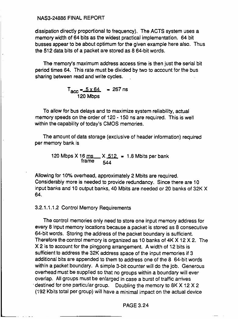
NAS3-24886 FINAL REPORT
dissipation directly proportional to frequency). The ACTS system uses a
memory width of 64 bits as the widest practical implementation. 64 bit
busses appear to be about optimum for the given example here also. Thus
the 512 data bits of a packet are stored as 8 64-bit words.
The memory's maximum address access time is then just the serial bit
period times 64. This rate must be divided by two to account for the bus
sharing between read and write cycles.
Tac c=.5x64 = 267ns
120 Mbps
To allow for bus delays and to maximize system reliability, actual
memory speeds on the order of 120 - 150 ns are required. This is well
within the capability of today's CMOS memories.
The amount of data storage (exclusive of header information) required
per memory bank is
120 Mbps X16 ms X 512 = 1.8 Mbits per bankframe 544
Allowing for 10% overhead, approximately 2 Mbits are required.
Considerably more is needed to provide redundancy. Since there are 10
input banks and 10 output banks, 40 Mbits are needed or 20 banks of 32K X64.
3.2.1.1.1.2 Control Memory Requirements
The control memories only need to store one input memory address for
every 8 input memory locations because a packet is stored as 8 consecutive
64-bit words. Storing the address of the packet boundary is sufficient.
Therefore the control memory is organized as 10 banks of 4K X 12 X 2. The
X 2 is to account for the pingpong arrangement. A width of 12 bits is
sufficient to address the 32K address space of the input memories if 3
additional bits are appended to them to address one of the 8 64-bit words
within a packet boundary. A simple 3-bit counter will do the job. Generous
overhead must be supplied so that no groups within a boundary will ever
overlap. All groups must be enlarged in case a burst of traffic arrives
' destined for one particular group. Doubling the memory to 8K X 12 X 2
(192 Kbits total per group) will have a minimal impact on the actual device
PAGE 3.24
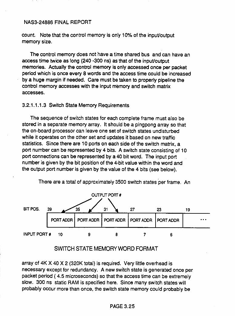
NAS3-24886 FINAL REPORT
count. Note that the control memory is only 10% of the input/output
memory size.
The control memory does not have a time shared bus and can have an
access time twice as long (240 -300 ns) as that of the input/output
memories. Actually the control memory is only accessed once per packet
period which is once every 8 words and the access time could be increased
by a huge margin if needed. Care must be taken to properly pipeline the
control memory accesses with the input memory and switch matrix
accesses.
3.2.1.1.1.3 Switch State Memory Requirements
The sequence of switch states for each complete frame must also be
stored in a separate memory array. It should be a pingpong array so that
the on-board processor can leave one set of switch states undisturbed
while it operates on the other set and updates it based on new traffic
statistics. Since there are 10 ports on each side of the switch matrix, a
port number can be represented by 4 bits. A switch state consisting of 10
port connections can be represented by a 40 bit word. The input port
number is given by the bit position of the 4-bit value within the word and
the output port number is given by the value of the 4 bits (see below).
There are a total of approximately 3500 switch states per frame. An
BFrPOS.
OUTPUTPORT#
PORTADDRI PORTADDR PORTADDR
I
IINPUT PORT # 10
27 23 19
I PORTADDR PORTADDRI9 8 7 6
SWITCH STATE MEMORY WORD FORMAT
array of 4K X40 X 2 (320K total) is required. Very little overhead is
necessary except for redundancy. A new switch state is generated once per
packet period ( 4.5 microseconds) so that the access time can be extremely
slow. 300 ns static RAM is specified here. Since many switch states will
probably occur more than once, the switch state memory could probably be
PAGE 3.25
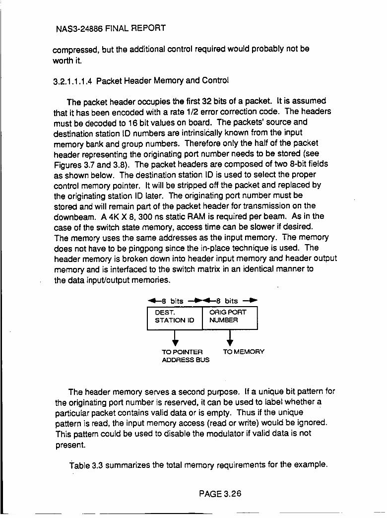
NAS3-24886 FINAL REPORT
compressed, but the additional control required would probably not be
worth it.
3.2.1.1.1.4 Packet Header Memory and Control
The packet header occupies the first 32 bits of a packet. It is assumed
that it has been encoded with a rate 1/2 error correction code. The headers
must be decoded to 16 bit values on board. The packets' source and
destination station ID numbers are intrinsically known from the input
memory bank and group numbers. Therefore only the half of the packet
header representing the originating port number needs to be stored (see
Figures 3.7 and 3.8). The packet headers are composed of two 8-bit fieldsas shown below. The destination station ID is used to select the proper
control memory pointer. It will be stripped off the packet and replaced by
the originating station ID later. The originating port number must be
stored and will remain part of the packet header for transmission on the
downbeam. A 4K X 8, 300 ns static RAM is required per beam. As in the
case of the switch state memory, access time can be slower if desired.
The memory uses the same addresses as the input memory. The memory
does not have to be pingpong since the in-place technique is used. The
header memory is broken down into header input memory and header output
memory and is interfaced to the switch matrix in an identical manner to
the data input/output memories.
_1--8 bits ---1l=.41--8 bits --4))
STATION ID NUMBER
TO POINTER TO MEMORY
ADDRESS BUS
The header memory serves a second purpose. If a unique bit pattern for
the originating port number is reserved, it can be used to label whether a
particular packet contains valid data or is empty. Thus if the unique
pattern is read, the input memory access (read or write) would be ignored.
This pattern could be used to disable the modulator if valid data is not
present.
Table 3.3 summarizes the total memory requirements for the example.
PAGE 3.26
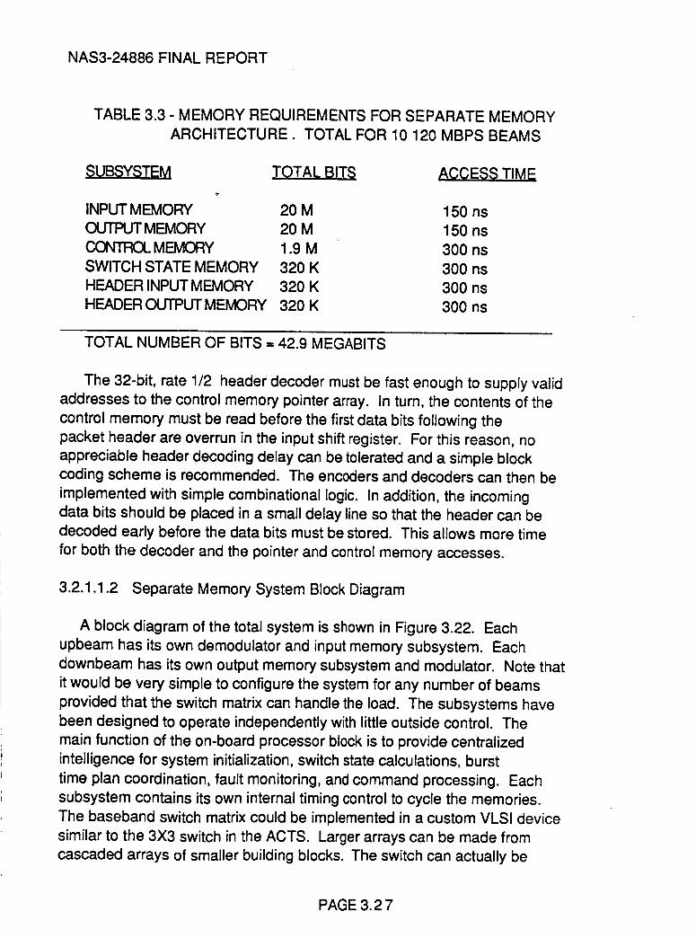
NAS3-24886 FINAL REPORT
TABLE 3.3 - MEMORY REQUIREMENTS FOR SEPARATE MEMORYARCHITECTURE. TOTAL FOR 10 120 MBPS BEAMS
INPUTMEMORYOUTPUTMEMORY_ MEMORYSWITCH STATE MEMORYHEADER INPUTMEMORYHEADEROUTPUTMEMORY
m ACCESS TIME
20 M 150 ns
20 M 150 ns
1.9 M 300 ns
320 K 300 ns
320 K 300 ns
320 K 300 ns
TOTAL NUMBER OF BITS = 42.9 MEGABITS
The 32-bit, rate 1/2 header decoder must be fast enough to supply valid
addresses to the control memory pointer array. In turn, the contents of the
control memory must be read before the first data bits following the
packet header are overrun in the input shift register. For this reason, no
appreciable header decoding delay can be tolerated and a simple blockcoding scheme is recommended. The encoders and decoders can then be
implemented with simple combinational logic. In addition, the incoming
data bits should be placed in a small delay line so that the header can be
decoded early before the data bits must be stored. This allows more time
for both the decoder and the pointer and control memory accesses.
3.2.1.1.2 Separate Memory System Block Diagram
A block diagram of the total system is shown in Figure 3.22. Each
upbeam has its own demodulator and input memory subsystem. Each
downbeam has its own output memory subsystem and modulator. Note that
it would be very simple to configure the system for any number of beams
provided that the switch matrix can handle the load. The subsystems have
been designed to operate independently with little outside control. The
main function of the on-board processor block is to provide centralized
intelligence for system initialization, switch state calculations, burst
time plan coordination, fault monitoring, and command processing. Each
subsystem contains its own internal timing control to cycle the memories.
The baseband switch matrix could be implemented in a custom VLSI device
similar to the 3X3 switch in the ACTS. Larger arrays can be made from
cascaded arrays of smaller building blocks. The switch can actually be
PAGE 3.2 7
NAS3-24886 FINAL REPORT
much slower than the ACTS switch. Switch states change only once every
4.5 usec. The only tight timing requirement is to minimize the settling
time when a new switch state is selected. One possibility is to disable the
bit stream while the switch is changing states. Upbeam data could build up
in a FIFO while it is waiting for the switch to change and then data can be
read from the FIFO at a rate slightly faster than 120 Mbps in order to catch
up. Thus the switch can be implemented with high speed CMOS technology.
Refer to Table 3.4 for a summary of devices and power dissipation for each
subsystem. Note that the memory power dissipation figures given assume a
10:1 power savings when the RAMs are not chip selected. Most CMOS static
RAMs have such a power down feature. The memories listed are the
standard sizes currently available. Radiation hardening has not beenassumed.
3.2.1.1.2.1 Input Subsystem Block Diagram
The input memory subsystem is shown in Figure 3.23. Serial data
arriving from the demod is sent to a unique word (UW) detector to detect
the proper frame synchronization. Every Input subsystem must be
synchronized to the same internal bit and frame clocks or the switch will
not work properly. The framing information from the UW detector is sent
to two different devices. It is sent to a 32-bit FIFO which serves three
purposes. The FIFO aligns the bits with the frame clock (there should not
be more than about 4 bits of ambiguity) and it delays the dat_[ to allow time
for control address decoding and generation. It also acts as a buffer during
switch state transitions as discussed above. The framing information is
also supplied to the block decoder which decodes the packet header
information. The decoder is implemented as a custom VLSl device
containing a 32-bit serial to parallel input register, a 32-bit parallel
decoder, and a 16-bit output latch.
The delayed data bits from the FIFO are converted to parallel in a 64-bit
serial to parallel register. The register also has an output latch to hold the
word during a write to the input memory. This device will require 4 16-bit
custom chips as designed for the ACTS. The input memory has a
bidirectional bus that receives data from the S/P register and writes data
to a P/S register connected to the switch matrix. The P/S register can use
the same 4 custom chips by just changing the inputs to their control pins.
Note that the FIFO, UW detector, decoder, and the S/P and P/S registers
must all operate at 120 Mbps, a rate presently too fast for CMOS
implementation (the ACTS uses ECL technology for this application).
PAGE 3.28
NAS3-24886 FINAL REPORT
The control memory pointers comprise another custom VLSI chip. It is
arranged as an array of 10 13-bit read pointers and 10 13-bit write
pointers. The device has its own increment logic and separate read and
write pointer output latches. The pointers are selected from one of two
sources. A pointer is selected for control memory write cycles from the
switch state memory. A pointer is selected for control memory read cycles
from the destination address decoded from the header (the upper 8 bits of
the decoder output latch).
The pointer latches are connected to the control memory address bus.
The control memory data bus is routed to the upper 12 bits of the input
memory address bus. It is also tied to the address bus of the originating
port number (header) memory. The control memory data bus is also looped
back to itself for "in-place" addressing. The control memory latch is used
to hold a value just read so it can be written back into the control memory
at a new address. The lower 3 bits of the input memory address bus are
connected to a 3-bit modulo 8 counter which increments every time a new
64-bit word within a packet is transferred. Note that the on-board
processor can also drive the control memory address bus for initialization
and diagnostics. It is assumed that the timing signals (memory read and
write strobes, bit clocks, etc.) and control logic can be implemented in 1 or
2 medium density semi-custom VLSI devices.
3.2.1.1.2.2 Output Subsystem Block Diagram
The output memory subsystem block diagram is shown in Figure 3.24. It
is very straightforward and only requires several devices. The S/P register
consists of the same 4 16-bit devices in the input subsystem and converts
serial data from the switch matrix to parallel words for the output
memory. Words are read from the output memory into the P/S register
where they are sent to the downbeam modulator. Again, the same 4 custom
devices are used for the P/S register. The P/S register can also be loaded
from the packet header memory. The header memory is read by a custom
block encoder chip. A hard-wired 8-bit value is also connected to the block
encoder to program the originating station ID. The header memory is
connected to the output memory data bus and is written from the same S/P
register. The output memory is addressed by a custom address generator
chip. The chip consists of a 15-bit counter, separate read and write
pointers, and an output latch. It is interfaced to the on-board processor for
initialization and diagnostics. The output memory subsystem also has its
PAGE 3.29
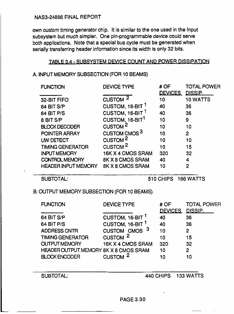
NAS3-24886 FINAL REPORT
own custom timing generator chip. It is similar to the one used in the Input
subsystem but much simpler. One pin-programmable device could serve
both applications. Note that a special bus cycle must be generated when
serially transferring header information since its width is only 32 bits.
TABLE 3.4 - SUBSYSTEM DEVICE COUNT AND POWER DISSIPATION
A. INPUT MEMORY SUBSECTION (FOR 10 BEAMS)
FUNCTION
32-BIT FIFO
64 BIT SIP
64 BIT P/S
8 BIT S/P
BLOCK DECODER
POINTER ARRAY
UW DETECT
TIMING GENERATOR
INPUT MEMORY
_QL MEMORY
HEADER INPUT MEMORY
DEVICE TYPE # OF TOTAL POWER
DEVICES DJ JE. CUSTOM 2 10 10 WATTS
CUSTOM, 16-BIT 1 40 36
CUSTOM, 16-BIT 1 40 36
CUSTOM, 16-BIT 1 10 9
CUSTOM 2 10 10
CUSTOM CMOS 3 10 2
CUSTOM 2 10 10
CUSTOM 2 10 15
16K X 4 CMOS SRAM 320 32
8K X 8 CMOS SRAM 40 4
8K X 8 CMOS SRAM 10 2
SUBTOTAL: 510 CHIPS 166 WATTS
B. OUTPUT MEMORY SUBSECTION (FOR 10 BEAMS)
FUNCTION DEVICE TYPE # OF TOTAL POWER
DEVICES DISSIP,CUSTOM, 16-BIT 1 40 36
CUSTOM, 16-BIT 1 40 36
CUSTOM CMOS 3 10 2
CUSTOM 2 10 15
16K X 4 CMOS SRAM 320 32
10 2
10 10
64 BIT SIP
64 BIT P/S
ADDRESS CNTR
TIMING GENERATOR
OUTPUT MEMORY
HEADER OUTPUT MEMORY 8K X 8 CMOS SRAM
BLOCK ENCODER CUSTOM 2
SUBTOTAL: 440 CHIPS 133 WATTS
PAGE 3.30
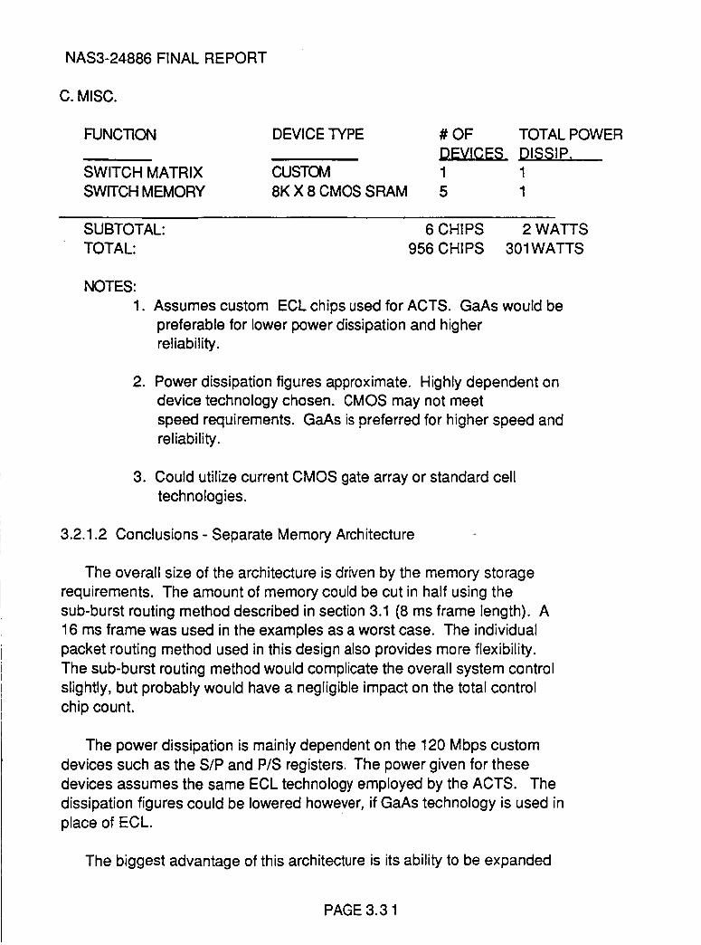
NAS3-24886 FINAL REPORT
C. MISC.
FUNCTION
SWITCH MATRIXSWITCHMEMORY
DEVICETYPE # OF TOTAL POWERDEVICES DISSIP.
CUSTOM 1 1
8K X 8 CMOS SRAM 5 1
SUBTOTAL: 6 CHIPS 2 WATTS
TOTAL: 956 CHIPS 301WATTS
NOTES:
1. Assumes custom ECL chips used for ACTS. GaAs would be
preferable for lower power dissipation and higher
reliability.
. Power dissipation figures approximate. Highly dependent on
device technology chosen. CMOS may not meet
speed requirements. GaAs is preferred for higher speed and
reliability.
3. Could utilize current CMOS gate array or standard cell
technologies.
3.2.1.2 Conclusions - Separate Memory Architecture
The overall size of the architecture is driven by the memory storage
requirements. The amount of memory could be cut in half using the
sub-burst routing method described in section 3.1 (8 ms frame length). A
16 ms frame was used in the examples as a worst case. The individual
packet routing method used in this design also provides more flexibility.
The sub-burst routing method would complicate the overall system control
slightly, but probably would have a negligible impact on the total control
chip count.
The power dissipation is mainly dependent on the 120 Mbps custom
devices such as the S/P and P/S registers. The power given for these
devices assumes the same ECL technology employed by the ACTS. The
dissipation figures could be lowered however, if GaAs technology is used in
place of ECL.
The biggest advantage of this architecture is its ability to be expanded
PAGE 3.3 1
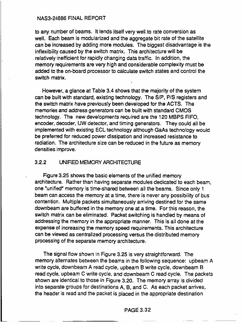
NAS3-24886 FINAL REPORT
to any number of beams. It lends itself very well to rate conversion as
well. Each beam is modularized and the aggregate bit rate of the satellite
can be increased by adding more modules. The biggest disadvantage is the
inflexibility caused by the switch matrix. This architecture will be
relatively inefficient for rapidly changing data traffic. In addition, the
memory requirements are very high and considerable complexity must be
added to the on-board processor to calculate switch states and control the
switch matrix.
However, a glance at Table 3.4 shows that the majority of the system
can be built with standard, existing technology. The S/P, P/S registers and
the switch matrix have previously been developed for the ACTS. The
memories and address generators can be built with standard CMOS
technology. The new developments required are the 120 MBPS FIFO,
encoder, decoder, UW detector, and timing generators. They could all be
implemented with existing ECL technology although GaAs technology would
be preferred for reduced power dissipation and increased resistance to
radiation. The architecture size can be reduced in the future as memory
densities improve.
3.2.2 UNIRED MEMORY ARCHITECTURE
Figure 3.25 shows the basic elements of the unified memory
architecture. Rather than having separate modules dedicatecl to each beam,
one "unified" memory is time-shared between all the beams. Since only 1
beam can access the memory at a time, there is never any possibility of bus
contention. Multiple packets simultaneously arriving destined for the same
downbeam are buffered in the memory one at a time. For this reason, the
switch matrix can be eliminated. Packet switching is handled by means of
addressing the memory in the appropriate manner. This is all done at the
expense of increasing the memory speed requirements. This architecture
can be viewed as centralized processing versus the distributed memory
processing of the separate memory architecture.
The signal flow shown in Figure 3.25 is very straightforward. The
memory alternates between the beams in the following sequence: upbeam A
write cycle, downbeam A read cycle, upbeam B write cycle, downbeam B
read cycle, upbeam C write cycle, and downbeam C read cycle. The packets
shown are identical to those in Figure 3.20. The memory array is divided
into separate groups for destinations A, B, and C. As each packet arrives,
the header is read and the packet is placed in the appropriate destination
PAGE 3.32
NAS3-24886 FINAL REPORT
group. The header selects one of three downbeam pointers which supplies
the next available memory address. The pointers are post-incremented
after each access. The packets are thus stored in their order of arrival
sorted by destination. No control memory is necessary because the packets
are sorted before they are written to the data memory. The memory is
output to the downbeams by initializing a second set of pointers to the top
of each group and then simply sequencing through each group in order. The
packets are sent to the downbeams in their order of arrival. This was not
the case for the separate memory architecture.
There is an inherent problem with the unified memory architecture if
only part of a packet is written to memory at a time. For example, if the
memory bus is 64 bits wide and a packet is 512 bits wide, then the packet
will require 8 separate memory writes. The problem is that the 8 writes
cannot occur consecutively because once 64 bits are written from one
upbeam the other upbeams must be processed to allow enough time for 64
more bits arrive. As a result, the packets can end up scrambled as shown in
Figure 3.26.
The figure shows 3 packets arriving on separate upbeams. All of them
are destined for downbeam A. The packets are shown broken down into
64-bit words labelled by their superscripts. The subscripts indicate
whether the packets originated from A, B, or C. The memory is alternately
written words from the S/P registers of upbeams A, B, and C. The words
are written to Group A of the unified memory in order. The final result is
that the 8 words from the 3 beams will become interleaved with each other
within the memory group. This presents a difficult problem when the
memory is being read. There is no way of knowing how to recover the
original packets because the number of packets being interleaved at a time
is random, depending on the traffic on each upbeam. If 8 packets arriving
on separate beams are destined for A, then they will all be interleaved.
One possible solution would be to write one entire packet to memory at
a time. 8 consecutive write cycles would occur for upbeam A followed by 8
consecutive write cycles for upbeam B, .... However this would require a
large amount of buffering to store all the incoming bits while the beams
wait their turn to access memory. In a 10-beam System each beam would
have to wait for 72 write cycles (4608 bits) before having access to
memory. This would require very large high-speed FIFOs on each beam.
Another solution to the problem is to use a more sophisticated memory
PAGE 3.33
NAS3-24886 FINAL REPORT
addressing scheme. When a packet is written to a group of memory, 8
consecutive locations must be reserved. A pointer must be dedicated to
that packet until all 8 words have been written. The next packet to be
written to that group must reserve another 8 locations. For an N beam
system a maximum of N pointers will be needed within a downbeam group.
N2 pointers are required for the whole system. Only N pointers are ever
used at a time but N 2 are needed to handle all possible source/destination
combinations.
An example of a 3 beam system is shown in Figure 3.27. A pointer
counter is required within each group to select one of the 3 pointers. This
means there is another level of indirection for memory accesses. The
pointers within group A are initialized to 000, 008, and 010. Group B of the
memory starts at address 100. The three B pointers are initialized to 100,
108, and 110. Similarly, the group C pointers are initialized to 200, 208,
and 210. Thus the pointers point to the first 3 8-word boundaries within
each group. The 3 pointer counters are initially zeroed.
Figure 3.27 shows 3 packets destined for A. The packet arriving from A
will access the first pointer counter, store the first packet word in
location 000, increment the first A pointer to 001 and increment the A
pointer counter. The pointer counter will now point to the second A pointer
and the first word of the packet arriving from B will be stored in location
008. Likewise the second A pointer will be incremented to 009 and the
pointer counter will again be incremented. The first word of the packet
from C will be stored in location 010 in a similar manner. Then the pointer
counters will be reset and the second words arriving from A, B, and C will
be stored in locations 001,009, and 011 respectively. Once all 8 words of
each packet have been loaded, the entire pointer array must be updated to
get ready for the next wave of new packets. The pointers are updated
according to the maximum value attained by the respective pointer counter
during the last packet period. In this case the highest memory location
filled was 017 by the last word of the packet from C. The A pointers must
then be reinitialized to 018, 020, and 028. The first A pointer is
incremented by 1+8N, where N = the maximum value latched by the pointer
counter. The second A pointer is incremented by 1+8(N+1) and the third A
pointer is incremented by 1+8(N+2). Note that the three pointers within
each group always differ by8 from each other. All the pointers will not be
used during any given packet period but they must all be initialized in case
many incoming packets are simultaneously destined for the same group.
PAGE 3.34
NAS3-24886 FINAL REPORT
The pointer logic must have a speed equal to the memory access time
and can easily be implemented in a single semi-custom logic device.
Separate output pointers will be required but they are very simple. Only 1
pointer is required per group since more than 1 packet cannot be written to
the same destination at the same time. These pointers can be implemented
in the same logic device.
The biggest advantage of this architecture is the tremendous flexibilityand simplicity resulting from the elimination of the switch matrix. The
switch matrix counts on the fact that a certain number of packets will
arrive on each upbeam destined for the various downbeams and no more.
The unified memory architecture does not care about the distribution of
packets between the various beams. For example, all the packets arriving
on upbeam A could be destined for downbeam B during one frame and
destined for downbeam C during the next frame. In fact, the aggregate sum
of all packets arriving destined for a certain downbeam could temporarily
exceed the capacity of the downbeam as long as the number of packets forthat destination decreases during the next frame. Extra overhead must be
included in each memory group to handle these short-term overloads. The
separate memory architecture overloaded if any one upbeam had too manypackets for one destination (switch overload) but the unified architecture
only overloads if the aggregate upbeam traffic for a given destination
exceeds the destination's downbeam overload capacity (memory overload).
3.2.2.1 Unified Memory Hardware Implementation
For purposes of comparison, the same design example of 10 120 Mbpsbeams given in section 3.2.1.1 will be used.
3.2.2.1.1 System Memory Requirements
The unified memory architecture only has two separate banks of
memory: Data memory and Header memory. The memories will have the
same 64-bit width as discussed in the separate memory architecture. The
267 ns access time calculated for the separate memory case (assuming
time-sharing of the memory between read and write cycles) must be
divided by 10 to account for time-sharing of the memory between 10
beams. This gives an access time, Tac c = 27 ns, not including any margin
between adjacent bus cycles or any safety factor. Such a speed is
impractical for a large memory array, especially if CMOS is desired. Such a
large number of bus lines switching at those speeds would cause very large
PAGE 3.35
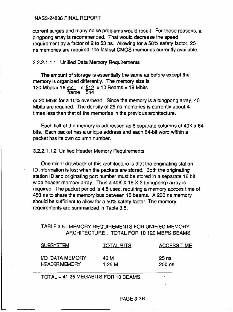
NAS3-24886 FINAL REPORT
current surges and many noise problems would result. For these reasons, a
pingpong array is recommended. That would decrease the speed
requirement by a factor of 2 to 53 ns. Allowing for a 50% safety factor, 25
ns memories are required, the fastest CMOS memories currently available.
3.2.2.1.1.1 Unified Data Memory Requirements
The amount of storage is essentially the same as before except the
memory is organized differently. The memory size is
120 Mbps x16 ms x 512 x10 Beams=18 Mbitsframe 544
or 20 Mbits for a 10% overhead. Since the memory is a pingpong array, 40
Mbits are required. The density of 25 ns memories is currently about 4
times less than that of the memories in the previous architecture.
Each half of the memory is addressed as 8 separate columns of 40K x 64
bits. Each packet has a unique address and each 64-bit word within a
packet has its own column number.
3.2.2.1.1.2 Unified Header Memory Requirements
One minor drawback of this architecture is that the originating station
ID information is lost when the packets are stored. Both the originating
station ID and originating port number must be stored in a separate 16 bit
wide header memory army. Thus a 40K X 16 X 2 (pingpong) array is
required. The packet period is 4.5 usec, requiring a memory accces time of
450 ns to share the memory bus between 10 beams. A 200 ns memory
should be sufficient to allow for a 50% safety factor. The memory
requirements are summarized in Table 3.5.
TABLE 3.5 - MEMORY REQUIREMENTS FOR UNIFIED MEMORY
ARCHITECTURE. TOTAL FOR 10 120 MBPS BEAMS
I/O DATA MEMORY
HEADER MEMORY
ACCESS TIME
40 M 25 ns
1.25 M 200 ns
TOTAL = 41.25 MEGABITS FOR 10 BEAMS
PAGE 3.36
NAS3-24886 FINAL REPORT
3.2.2.1.2 Unified Memory System Block Diagram
A complete system block diagram of the unified memory architecture is
given in Figure 3.28 and a detailed diagram of the control sections is given
in Figure 3.29. Each beam has its own modulator, demodulator, and control
subsection. The address pointer array described in section 3.2.2 is
implemented in a single CMOS custom chip. The headers decoded by the
control subsections are multiplexed onto the control address bus and select
an input pointer from the pointer array. The input pointers are latched into
2 separate latches. One latch drives the data memory address bus and the
other drives the header memory address bus. The addresses change every
400 nsec so the internal logic does not have to be extremely fast. A modulo
8 counter is used to select 1 of 8 64-bit columns in the data memory array.
Data latched into the control subsection S/P registers is output to a 64-bit
multiplexed data bus and is written to the data memory. The header 8-bit
originating port numbers are also brought out on this bus and are stored in
the header memory. An 8-bit counter provides the originating station ID
number to the header memory.
Similarly, the output pointers are latched into 2 separate latches toaddress the data and header memories. Both header and data information
are multiplexed onto the same data bus and are written to the P/S
registers in the control subsections. Note that special shortened bus
cycles are required for the 16-bit header memory accesses. The bus timing
cycles are generated by a single custom timing chip. The chip must be very
high speed (> 40 MHz) but may be just within the capabilities of today's
CMOS technology. Refer to Table 3.6 for a summary of devices and power
dissipation for each subsystem.
PAGE 3.3 7

NAS3-24886 FINAL REPORT
TABLE 3.6 - SUBSYSTEM DEVICE COUNT AND POWER DISSIPATION-
UNIFIED MEMORY ARCHITECTURE
A. UNIFIED MEMORY SUBSECTION (FOR 10 BEAMS)
FUNCTION
POINTER ARRAY
TIMING GENERATOR
DATA M EMORY
HEADER MEMORY
MISC. COUNTERS
DEVICE TYPE
CUSTOM CMOS 3
CUSTOM 2
4K X 4 CMOS SRAM
8K X 8 CMOS SRAM
STANDARD ECL
# OF TOTAL POWER
DEVICES DISSIP.
10 2
1 5
2560 1000/3004
20 2
2 2
SUBTOTAL: 2593 CHIPS 1011/3114 WATTS
B. CONTROL SUBSECTION (FOR 10 BEAMS)
FUNCTION DEVICE TYPE # OF TOTAL POWER
DEVICES DISSIP.CUSTOM 2 10 10
CUSTOM, 16-BIT 1 40 36
CUSTOM, 16-BIT 1 40 36
CUSTOM 2 10 - 10
CUSTOM 2 10 10
CUSTOM 2 10 10
32-BIT FIFO
64 BIT S/P
64 BIT P/S
BLOCK ENCODER
BLOCK DECODER
UW DE'rECTOR
SUBTOTAL: 120 CHIPS 112 WATTS
TOTAL:
NOTES:
1.
.
2713 CHIPS 11234/423 WATTS
Assumes custom ECL chips used for ACTS. GaAs would be
preferable for lower power dissipation and higher
reliability.
Power dissipation figures approximate. Highly dependent on
device technology chosen. CMOS may not meet speed
requirements. GaAs is preferred for higher speed and
reliability.
PAGE 3.38
NAS3-24886 FINAL REPORT
3. Could utilize current gate array or standard cell technologies
4. First figure assumes no power down of SRAM devices.Second figure assumes 4:1 power savings when SRAM devicesare not chip selected.
3.2.2.1.3 Unified Memory Control Subsystem Block Diagram
The control subsection contains the same basic elements as the inputand output subsections of the separate memory architecture. A 32-bit FIFOtied to the demodulator is used for timing synchronization and to provideenough time delay for the header decoding process. A unique word detectordetects proper frame timing. A custom block decoder chip decodes theheader bits. The chip contains its own internal input S/P register andoutput parallel latch. The chip should be implemented with either GaAs orECL due to the speeds involved. The input data bits are converted to 64-bitwords by the custom 64-bit S/P register. Again, the 16-bit custom ECLdevices designed for the ACTS could be used. The same devices could alsobe used for the 64-bit P/S register which is loaded from the data memoryand sends a serial bit stream to the modulator. Note that this serialstream is multiplexed inside another custom chip, the block encoder. The16-bit header memory data bus writes to the block encoder and theresulting 32-bit words are latched in the internal P/S register. The mux
then selects either header or data bits as determined by the central timing
device. The encoder chip also has tight timing constraints and should beeither ECL or GaAs.
3.2.2.2 Conclusions- Unified Memory Architecture
The advantages in system efficiency have been shown for unifying the
system memory into one time-shared array. The packet switching becomes
trivial and is simply a matter of generating the proper memory addresses
in a single custom address generator device. The architecture is limited by
one single problem - that of obtaining fast enough memory devices. The
example given here probably represents the uppermost throughput limit.
Throughput is dependent only on the aggregate system bit rate, not on thenumber of beams or the individual beam bit rates.
The figures given in Table 3.6 are so much worse than those given for
the previous architecture because of the extremely fast memory speed
PAGE 3.3 9
NAS3-24886 FINAL REPORT
requirements. The higher speed RAMs have a 4:1 density disadvantage andthe power down savings are not so great. A separate power figure wasgiven for RAMs without a power-down feature because at the speedsinvolved, it is questionable whether the RAMs can be powered down at all.They may have to have their chip select lines constantly asserted. Thememory data busses would then be controlled by a separate output enableline which typically has a faster response time.
However, the removal of the switch state calculations from the
on-board processor system has not been factored in to Table 3.6. The
overall system has been tremendously simplified and the processor
requirements are mainly for system initialization, diagnostics, and
command control. The unified memory architecture would be the
architecture of choice if the aggregate bit rate was reduced from 1.2 Gbps
to about 200 Mbps. At the slower speed, denser 16K x4 120 ns CMOS RAMs
could be used, making the system device count and power dissipation better
than the separate memory architecture. Such a system could easily be
implemented with existing technology. Faster bit rates would require
major advances in memory technology such as the development of very
dense (16K X 4) GaAs SRAM.
3.2.3 ALTERNATIVE UNIFIED MEMORY ARCHITECTURE
One of the main drawbacks of the preceding unified memory architecture
was the necessity of pingpong memory. If the memory speed requirements
were substantially reduced then the "in-place" approach discussed in
section 3.2.1.1.1 could be implemented, thereby reducing the memory size
by a factor of two. This type of architecture is illustrated in Figure 3.30.
The basic principle is the same as for the separate memory architecture of
section 3.2.1. Since the control memories are time-shared between all the
upbeams, a separate bank of control memory is dedicated to each
downbeam. The memories are not partitioned into groups as before.
Consequently each control memory requires only a single pointer (that is, a
single read pointer and a single write pointer).
The data memory is simply filled in the order packets are received.
The data memory addresses are written to the proper control memory bank,
as determined by the packet header's destination addresses. The packets
are reordered when the memory is read out to the downbeams. As a result,
the overhead requirements of the data memory are substantially reduced.
An extra amount of overhead can be added at the bottom of the memory, to
PAGE 3.4 0
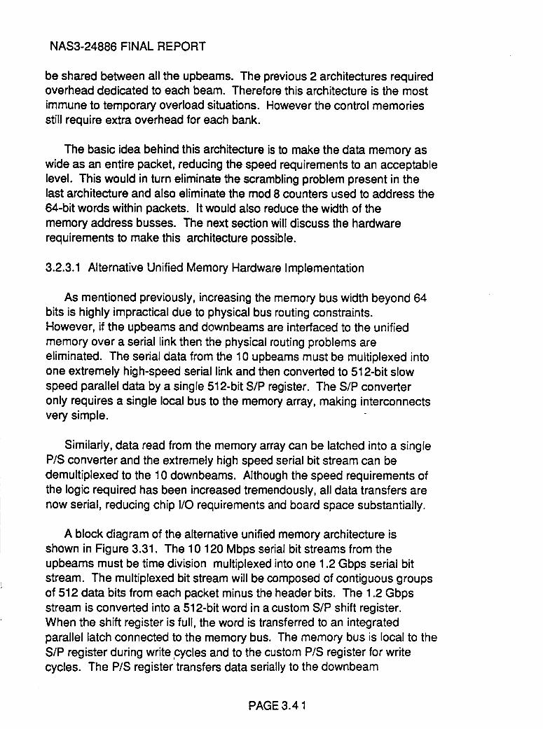
NAS3-24886 FINAL REPORT
be shared between all the upbeams. The previous 2 architectures requiredoverhead dedicated to each beam. Therefore this architecture is the most
immune to temporary overload situations. However the control memories
still require extra overhead for each bank.
The basic idea behind this architecture is to make the data memory as
wide as an entire packet, reducing the speed requirements to an acceptable
level. This would in turn eliminate the scrambling problem present in thelast architecture and also eliminate the mod 8 counters used to address the
64-bit words within packets. It would also reduce the width of the
memory address busses. The next section will discuss the hardware
requirements to make this architecture possible.
3.2.3.1 Alternative Unified Memory Hardware Implementation
As mentioned previously, increasing the memory bus width beyond 64
bits is highly impractical due to physical bus routing constraints.
However, if the upbeams and downbeams are interfaced to the unified
memory over a serial link then the physical routing problems are
eliminated. The serial data from the 10 upbeams must be multiplexed into
one extremely high-speed serial link and then converted to 512-bit slow
speed parallel data by a single 512-bit S/P register. The S/P converter
only requires a single local bus to the memory array, making interconnects
very simple.
Similarly, data read from the memory array can be latched into a single
P/S converter and the extremely high speed serial bit stream can be
demultiplexed to the 10 downbeams. Although the speed requirements of
the logic required has been increased tremendously, all data transfers are
now serial, reducing chip I/O requirements and board space substantially.
A block diagram of the alternative unified memory architecture is
shown in Figure 3.31. The 10 120 Mbps serial bit streams from the
upbeams must be time division multiplexed into one 1.2 Gbps serial bit
stream. The multiplexed bit stream will be composed of contiguous groups
of 512 data bits from each packet minus the header bits. The 1.2 Gbps
stream is converted into a 512-bit word in a custom S/P shift register.
When the shift register is full, the word is transferred to an integrated
parallel latch connected to the memory bus. The memory bus is local to the
S/P register during write cycles and to the custom P/S register for write
cycles. The P/S register transfers data serially to the downbeam
PAGE 3.4 1
NAS3-24886 FINAL REPORT
demultiplexer at a 1.2 Gbps rate. The memory bus is confined to a small
area, eliminating physical routing problems. Of course now the problem has
been shifted to one of developing a reliable digital mux and demux capable
of operating at a speed of 1.2 Gbps. The hardware will be analyzed in
further detail in the following sections.
PAGE 3.42
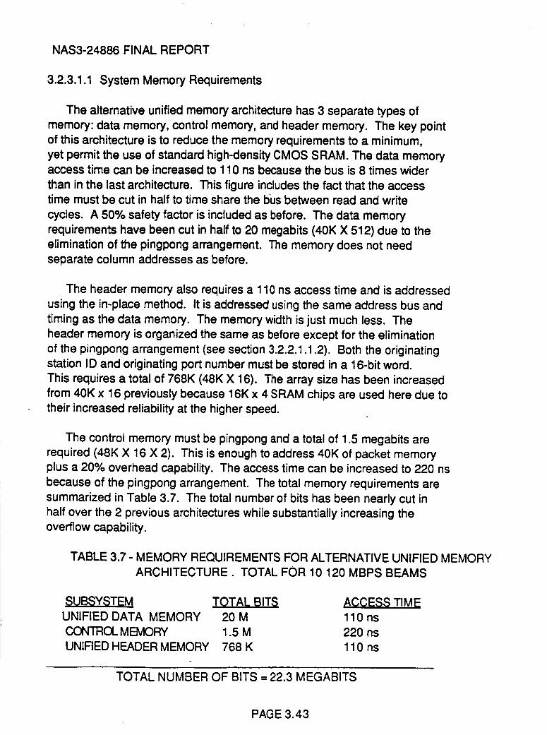
NAS3-24886 FINAL REPORT
3.2.3.1.1 System Memory Requirements
The alternative unified memory architecture has 3 separate types of
memory: data memory, control memory, and header memory. The key point
of this architecture is to reduce the memory requirements to a minimum,
yet permit the use of standard high-density CMOS SRAM. The data memoryaccess time can be increased to 110 ns because the bus is 8 times wider
than in the last architecture. This figure includes the fact that the access
time must be cut in half to time share the bus between read and write
cycles. A 50% safety factor is included as before. The data memory
requirements have been cut in half to 20 megabits (40K X 512) due to the
elimination of the pingpong arrangement. The memory does not need
separate column addresses as before.
The header; memory also requires a 110 ns access time and is addressed
using the in-place method. It is addressed using the same address bus and
timing as the data memory. The memory width is just much less. The
header memory is organized the same as before except for the elimination
of the pingpong arrangement (see section 3.2.2.1.1.2). Both the originating
station ID and originating port number must be stored in a 16-bit word.
This requires a total of 768K (48K X 16). The array size has been increased
from 40K x 16 previously because 16K x 4 SRAM chips are used here due to
their increased reliability at the higher speed.
The control memory must be pingpong and a total of 1.5 megabits are
required (48K X 16 X 2). This is enough to address 40K of packet memory
plus a 20% overhead capability. The access time can be increased to 220 ns
because of the pingpong arrangement. The total memory requirements are
summarized in Table 3.7. The total number of bits has been nearly cut in
half over the 2 previous architectures while substantially increasing the
overflow capability.
TABLE 3.7 - MEMORY REQUIREMENTS FOR ALTERNATIVE UNIFIED MEMORY
ARCHITECTURE . TOTAL FOR 10 120 MBPS BEAMS
UNIFIED DATA MEMORY 20 M
CONTROL MEMORY 1.5 M
UNIFIED HEADER MEMORY 768 K
ACCESS TIME
110 ns
220 ns
110 ns
TOTAL NUMBER OF BITS = 22.3 MEGABITS
PAGE 3.43
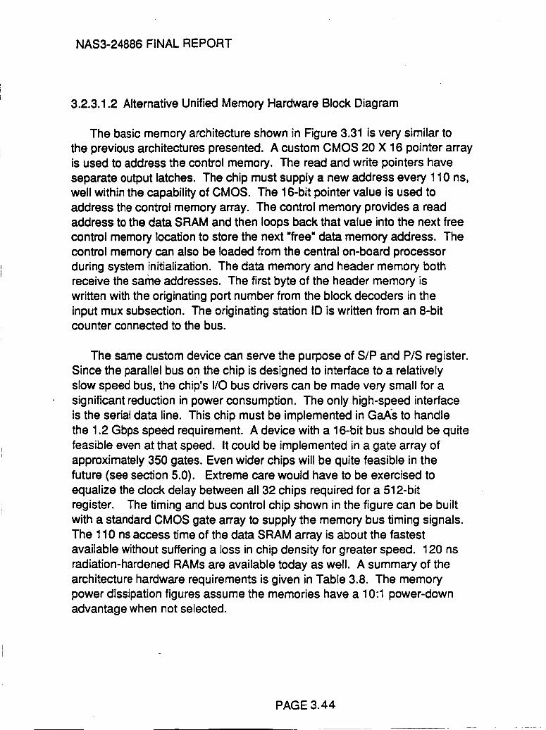
NAS3-24886 FINAL REPORT
3.2.3.1.2 Alternative Unified Memory Hardware Block Diagram
The basic memory architecture shown in Figure 3.31 is very similar to
the previous architectures presented. A custom CMOS 20 X 16 pointer array
is used to address the control memory. The read and write pointers have
separate output latches. The chip must supply a new address every 110 ns,
well within the capability of CMOS. The 16-bit pointer value is used to
address the control memory array. The control memory provides a read
address to the data SRAM and then loops back that value into the next free
control memory location to store the next "free" data memory address. The
control memory can also be loaded from the central on-board processor
during system initialization. The data memory and header memory both
receive the same addresses. The first byte of the header memory is
written with the originating port number from the block decoders in the
input mux subsection. The originating station ID is written from an 8-bitcounter connected to the bus.
The same custom device can serve the purpose of S/P and P/S register.
Since the parallel bus on the chip is designed to interface to a relatively
slow speed bus, the chip's I/O bus drivers can be made very small for a
significant reduction in power consumption. The only high-speed interface
is the serial data line. This chip must be implemented in GaAs to handle
the 1.2 Gbps speed requirement. A device with a 16-bit bus should be quite
feasible even at that speed. It could be implemented in a gate array of
approximately 350 gates. Even wider chips will be quite feasible in the
future (see section 5.0). Extreme care would have to be exercised to
equalize the clock delay between all 32 chips required for a 512-bit
register. The timing and bus control chip shown in the figure can be built
with a standard CMOS gate array to supply the memory bus timing signals.
The 110 ns access time of the data SRAM array is about the fastest
available without suffering a loss in chip density for greater speed. 120 ns
radiation-hardened RAMs are available today as well. A summary of the
architecture hardware requirements is given in Table 3.8. The memory
power dissipation figures assume the memories have a 10:1 power-down
advantage when not selected.
PAGE 3.44
NAS3-24886 FINAL REPORT
3.2.3.1.2.1 Alternative Unified Memory Serial Input Mux Block Diagram
A block diagram of the serial input mux is shown in Figure 3.32. 120
Mbps data from each beam is input to both a 544-bit serial FIFO and an
input subsystem. The_input subsystem contains a unique word detector chip
and a block decoder chip as in the previous architecture. Note that the
packet header information is stripped off separately and is not multiplexed
onto the serial bus. The FIFO is long enough to store an entire data packet
plus allow some time delay and also perform frame synchronization. Once
an entire packet has been loaded into the FIFOs, each FIFO in turn outputs512 bits at a rate of 1.2 Gbps. The FIFO read and write clocks are
generated by a custom GaAs timing chip. The chip is within the
capabilities of today's GaAs gate array technology but again, extreme care
must be taken to equalize the clock delays when interconnecting thedevices on a PC board.
The most difficult aspect of this entire architecture is the
implementation of the FIFOs, both because of their size and their speed.
Approximately 10,000 gates are required - more than five times today's
practical limits. In addition, the entire chip must operate at the maximum
1.2 Gbps clock rate, making interconnections within the chip very difficult.
The FIFOs could possibly be made by interconnecting 8 68-bit devices.
Power dissipation should not be too severe since the chip only has two
high-speed data pins. Of course this will have a serious impact on the
system parts count and power dissipation figures. Refer to section 5.0 for
a discussion of GaAs technology and its future.
3.2.3.1.2.2 Alternative Unified Memory Serial Output Mux Block Diagram
The serial output demux is shown in Figure 3.33. The FIFOs are identical
except that data is written into the FIFO at 1.2 Gbps and is read at 120
Mbps. The read and write clocks have been reversed. The timing generator
chip is essentially the same as in the input MUX. It is much easier to
implement because the output clocks are at a slower rate of 120 Mbps. The
timing generator chip enables the 1.2 Gbps serial data stream into one of
the 10 FIFOs at a time. The FIFOs output their data at a constant 120 Mbps
to the output subsystems. The output subsystems mux the data with the
data derived from a custom block decoder chip loaded from the header
memory. The block decoder chip is the same as for the previous
PAGE 3.45
NAS3-24886 FINAL REPORT
architecture. Again, the limiting factor of the demux is the ability to
produce a large FIFO at these speeds.
PAGE 3.46
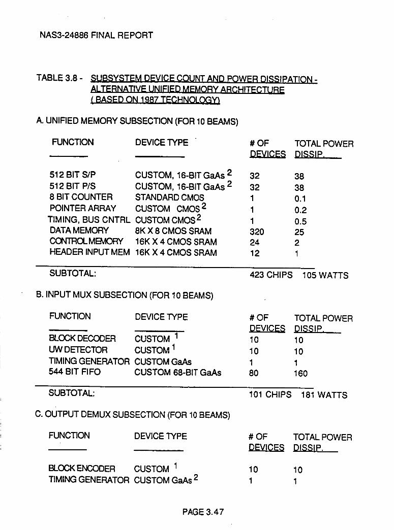
NAS3-24886 FINAL REPORT
TABLE 3.8 - SUBSYSTEM DEVICE COUNT AND POWER DISSIPATION-
ALTERNATIVE UNIFIED MEMORY ARCHITECTURF
( BASED ON 1987 TECHNOLOGY).
A. UNIFIED MEMORY SUBSECTION (FOR 10 BEAMS)
FUNCTION DEVICE TYPE # OF TOTAL POWER
DEVICES
512 BIT SIP
512 BIT P/S
8 BIT COUNTER
POINTER ARRAY
TIMING, BUS CNTRL
DATA MEMORY
C(]N3_OL MEMORY
HEADER INPUT MEM
CUSTOM, 16-BIT GaAs 2
CUSTOM, 16-BIT GaAs 2
STANDARD CMOS
CUSTOM CMOS 2
CUSTOM CMOS 2
8K X 8 CMOS SRAM
16K X 4 CMOS SRAM
16K X 4 CMOS SRAM
32 38
32 38
1 0.1
1 0.2
1 0.5
320 25
24 2
12 1
SUBTOTAL:
B. INPUT MUX SUBSECTION (FOR 10 BEAMS)
FUNCTION
BLOCK DECODER
UW DETECTOR
TIMING GENERATOR
544 BIT FIFO
DEVICE TYPE
CUSTOM 1
CUSTOM 1
CUSTOM GaAs
CUSTOM 68-BIT GaAs
423 CHIPS
# OF
VlCES10
10
1
8O
105 WATTS
TOTAL POWER
DISSIP.
10
10
1
160
SUBTOTAL:
C. OUTPUT DEMUX SUBSECTION (FOR 10 BEAMS)
FUNCTION DEVICE TYPE
BLOCK ENCODER CUSTOM 1
TIMING GENERATOR CUSTOM GaAs 2
101 CHIPS
10
1
181 WATTS
TOTAL POWER
DISSIP.
10
1
PAGE 3.47
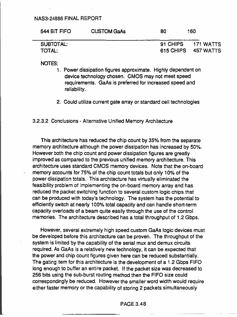
NAS3-24886 FINAL REPORT
544 BIT FIFO CUSTOM GaAs 8O 160
SUBTOTAL:
TOTAL:
91 CHIPS
615 CHIPS
171 WATTS
457 WATTS
NOTES:
1. Power dissipation figures approximate. Highly dependent on
device technology chosen. CMOS may not meet speed
requirements. GaAs is preferred for increased speed and
reliability.
2. Could utilize current gate array or standard cell technologies
3.2.3.2 Conclusions - Alternative Unified Memory Architecture
This architecture has reduced the chip count by 35% from the separate
memory architecture although the power dissipation has increased by 50%.
However both the chip count and power dissipation figures are greatly
improved as compared to the previous unified memory architecture. This
architecture uses standard CMOS memory devices. Note that the on-board
memory accounts for 75% of the chip count totals but only 10% of the
power dissipation totals. This architecture has virtually eliminated the
feasibility problem of implementing the on-board memory array and has
reduced the packet switching function to several custom logic chips that
can be produced with today's technology. The system has the potential to
efficiently switch at nearly 100% total capacity and can handle short-term
capacity overloads of a beam quite easily through the use of the control
memories. The architecture described has a total throughput of 1.2 Gbps.
However, several extremely high speed custom GaAs logic devices must
be developed before this architecture can be proven. The throughput of the
system is limited by the capability of the serial mux and demux circuits
required. As GaAs is a relatively new technology, it can be expected that
the power and chip count figures given here can be reduced substantially.
The gating item for this architecture is the development of a 1.2 Gbps FIFO
long enough to buffer an entire packet. If the packet size was decreased to
256 bits using the sub-burst routing method then the FIFO size could
correspondingly be reduced. However the smaller word width would require
either faster memory or the capability of storing 2 packets simultaneously
PAGE 3.48
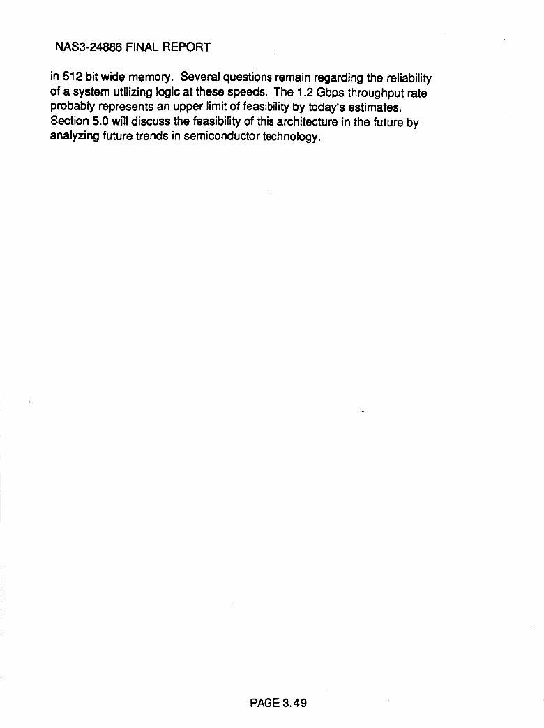
NAS3-24886 FINAL REPORT
in 512 bit wide memory. Several questions remain regarding the reliability
of a system utilizing logic at these speeds. The 1.2 Gbps throughput rate
probably represents an upper limit of feasibility by today's estimates.
Section 5.0 will discuss the feasibility of this architecture in the future by
analyzing future trends in Semiconductor technology.
PAGE 3.49
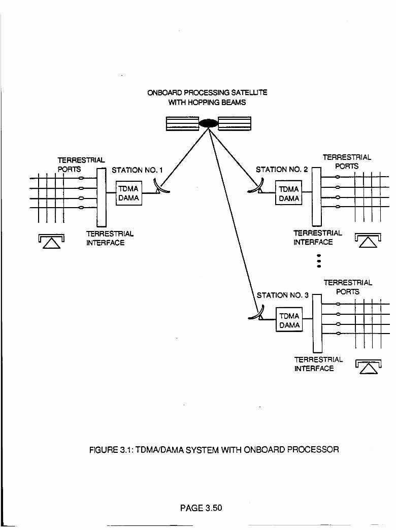
ONBOARD PROCESSING SATELLITE
WITH HOPPING BEAMS
TERRESTRIAL
PORTS
O
STATION NO. 1
TERRESTRIAL
INTERFACE
STATION NO. 2
TERRESTRIALPORTS
1-TERRESTRIALINTERFACE _-LJ
Z_.__
O
O
Q
STATION NO. 3I
TERRESTRIALPORTS
I
---,-,,0
I
TERRESTRIALINTERFACE
!
II
l
FIGURE 3.1: TDMA/DAMA SYSTEM WITH ONBOARD PROCESSOR
PAGE 3.50
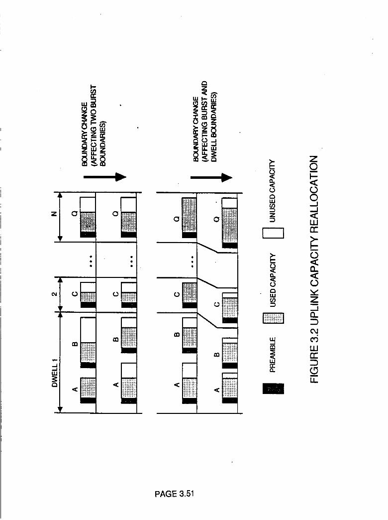
Z
OJ
i
..J
w
m
' IZ
v O.
° o• ILl
O_ --J
z <
ii_i:i:ii__
_iiiiliii_iii_i
I I
I
I
I
I
m
I
i
ii2iiiiiiiii2iii21iil_ I::::::::::
!iiiiiii!!iiii
i
Ii
_iiiii!iiiiil]!i_i!i
i::iii::i::?:i::iii_!_i_:::::!:!:i:_:::i::::
I
_ vtlJ_ Z
...!
_n I.t.I
i
U..
PAGE 3.51
0
m
i:i$i:!:i:i:i$i:]
i
<: I
m I
m I
m
<::::::::.::::_:::
iiiiiiiii!i!!iiii!!i
:{:i:i:{:!:i:i:!:_
0
m
0
0
_ w0
_ w
0
w
ii!!iiiiiiiliMili! =
--JW
ZZ
"1"0I.U
.J
...ILU
rr,<0rnZ0
LU
rr"
LL
A
ujuJ
u- I_
_z__.o
PAGE 3.52
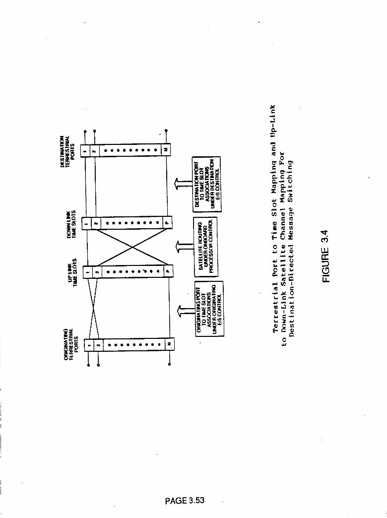
|"=" I" °'°"_|_I I "'"'i _ .
"]I _§
|_._|_
, Jl IIn, I_
of=4
!
D
c
0
c
P.. _ ,,c
0
*_ 4=I
_ ¢'.J
e_o
m
PAGE 3.53
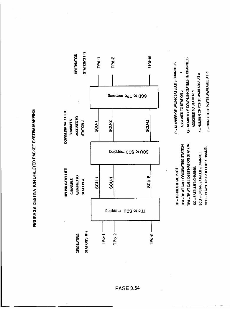
6u!ddeku nos ol OcLL
II
ii -,0n
• i=-
I II i
0 0
PAGE 3.54
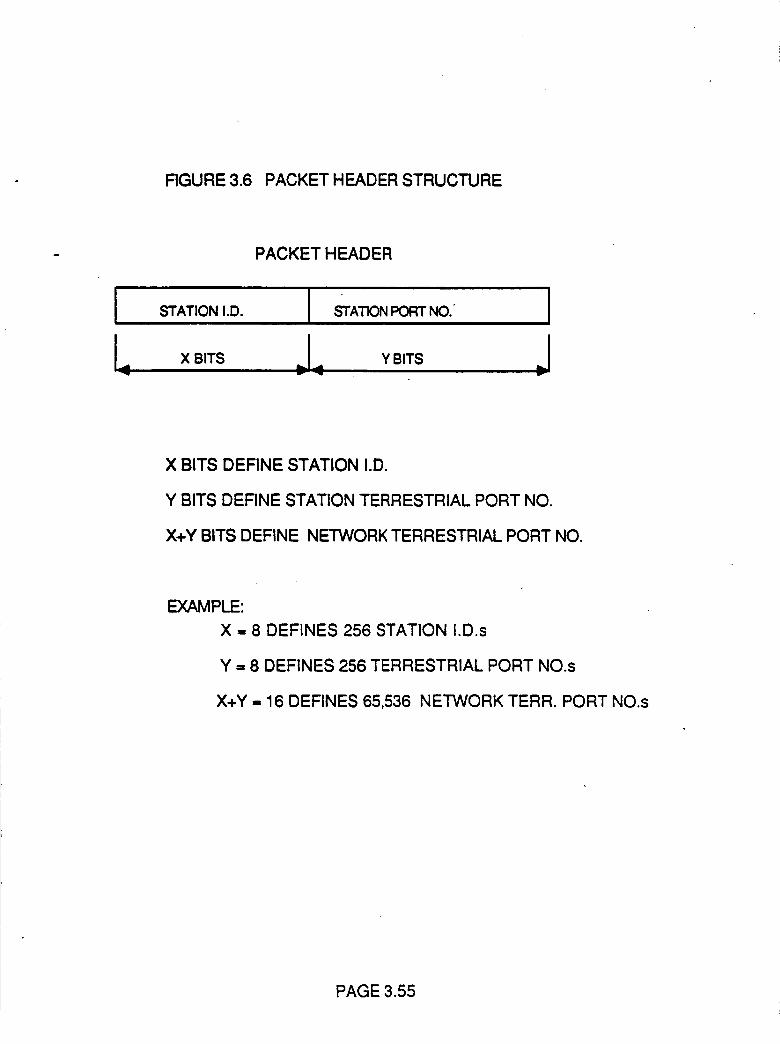
FIGURE 3.6 PACKET HEADER STRUCTURE
PACKET HEADER
STATION I.D. I s'rA'nON rrNo IXBITS J__ YBIT$ ..I
X BITS DEFINE STATION I.D.
Y BITS DEFINE STATION TERRESTRIAL PORT NO.
X+Y BITS DEFINE NETWORK TERRESTRIAL PORT NO.
EXAMPLE:
X = 8 DEFINES 256 STATION I.D.s
Y = 8 DEFINES 256 TERRESTRIAL PORT NO.s
X+Y = 16 DEFINES 65,536 NETWORK TERR. PORT NO.s
PAGE 3.55
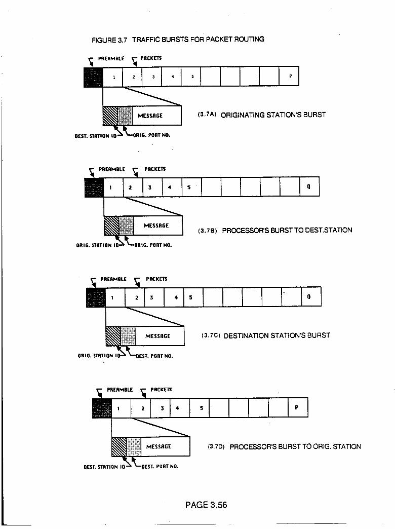
FIGURE 3.7 TRAFFIC BURSTS FOR PACKET ROUTING
PREAMBLE PACKETS
(3.7A) ORIGINATING STATION'S BURST
O(ST. STATION I0 PORT NO.
R(AMBL( _ PACKETS
m. 1,131..I,I I I I I- IQI
__ (3.7C) DESTINATION STATION'S BURSTiiii!ii!iiiii!iii
o,,, ST.,,o. ,_o_i_--oest.PORT.O.
R(AMRL( _ PACKETS
o,,,.,,,,,o,,_t-o,,,,po,,,o.
(3.7D) PROCESSOR'S BURST TO ORIG. STATION
PAGE 3.56
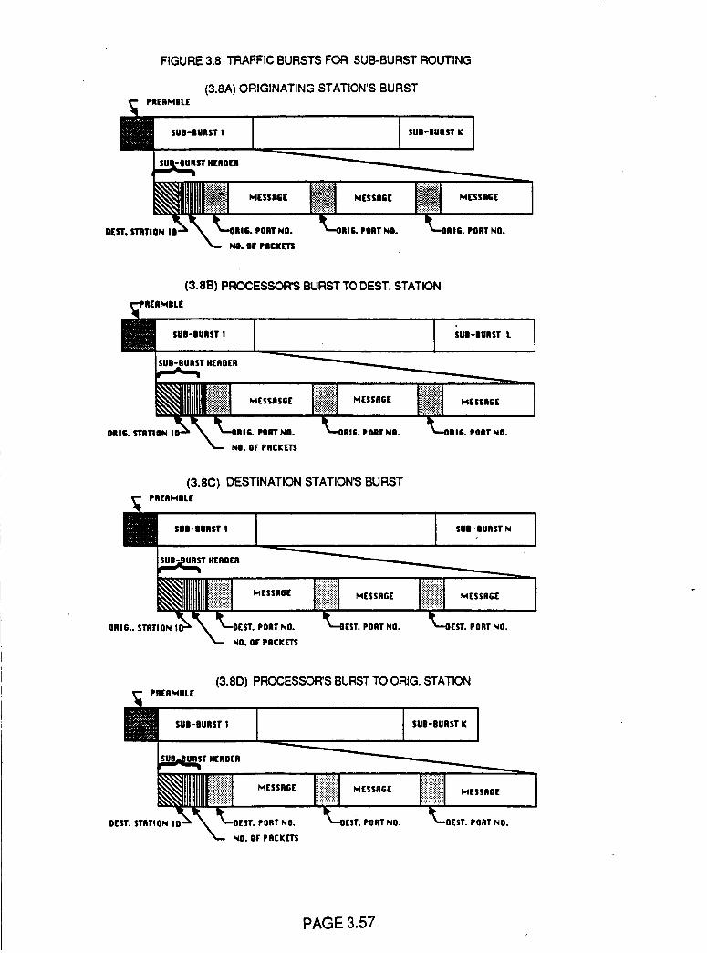
FIGURE 3.8 TRAFFIC BURSTS FOR SUB-BURST ROUTING
(3.8A) ORIGINATING STATION'S BURST
_!.."._1 MESSAGr
LOBIIL PORT NO.
SUB-BURST KPl [AMBLESUB-BURST I I
:'_ '_i MESSAGE
,,,,.,,,,,=,,,",__L-:,;:::::a_1 M''-'' I"'"LRIG. PORT NO.
(3.8B) PROCESSORS BURST TO DEST. STATION
RMIIL(
SUB-BURST 1 I
T HEAO(R
llllllV0RI U. STBTION IDI_ RLoIR IS. PORT NO.
_-- NO. OIr PACKETS
SUB-BURST L I
::;:;:;:::;;;:::;:
_;_:_:i._¢!1 MESSAGE.'-:,:.:_.:_:.
L,,,. PURT,,O. RIG. PORT NO.
(3.8C) DESTINATION STATION'S BURSTPREAMBLE
SUI-IURST I I
M(S [ _MESSAG(
I SUI-BUOSTN I
(3.8D) PROCESSOR'S BURST TO ORIG. STATION
iimm REAMBLE
SUB-BURST 1 I I SUB-BURST K
NlllllllllI_l----I!1---- I_ ---- I
PAGE 3.57
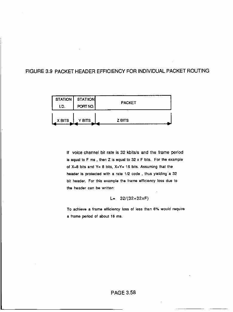
FIGURE 3.9 PACKET HEADER EFFICIENCY FOR INDIVIDUAL PACKET ROUTING
STATIONI.D.I STATIIONIPoRTNO'I PACKET I
If voice channel bit rate is 32 kbits/s and the frame period
is equal to F ms, then Z is equal to 32 x F bits. For the example
of X=8 bits and Y= 8 bits, X+Y= 16 bits. Assuming that the
header is protected with a rate 1/2 code , thus yieldinga 32
bit header. For this example the frame efficiency loss due to
the header can be written:
L= 32/(32+32xF)
To achieve a frame efficiency loss of less than 6% would require
a frame period of about 16 ms.
PAGE 3.58
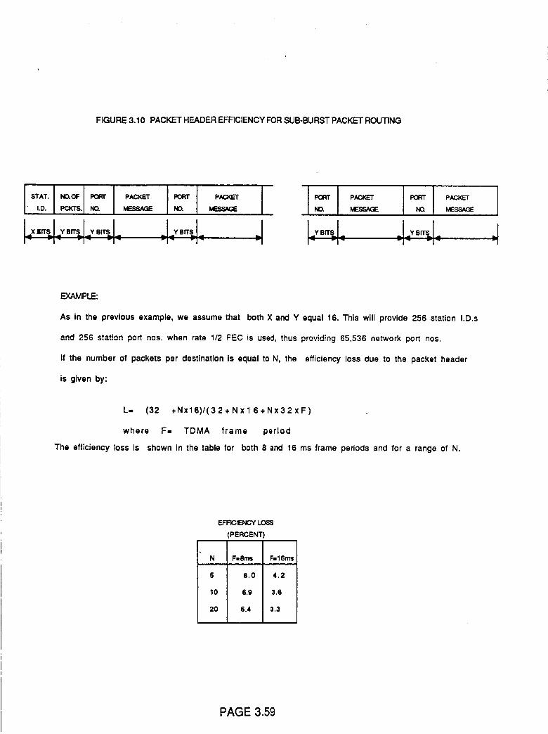
FIGURE 3.10 PACKET HEADER EFFICIENCY FOR SUB-BURST PACKET ROUTING
• ,.o. i Pc_rs.INO. I
i _ _1 _ _1 _ -i _ -i _ _1_
I:1-I I T Vl
MESSAGE
Jv I
EXAMPLE:
AS in the previous example, we assume that both X and Y equal 16. This will provide 256 station I.D.s
and 256 station port nos. when rate 112 FEC is used, thus providing 65,536 ne._vork port nos.
If the number of packets per destination is equal to N, the efficiency loss due to the packet header
is given by:
L= (32 +Nx16)/(32+ Nx 1 6+Nx32xF)
where F- TDMA frame period
The efficiency loss is shown in the table for both 8 and 16 ms frame periods and for a range of N.
EFFICIENCY
(PERCENT)
N F=8m$ F=16ms
5 8.0 4.2
10 6.9 3.6
20 6.4 3.3
PAGE 3.59
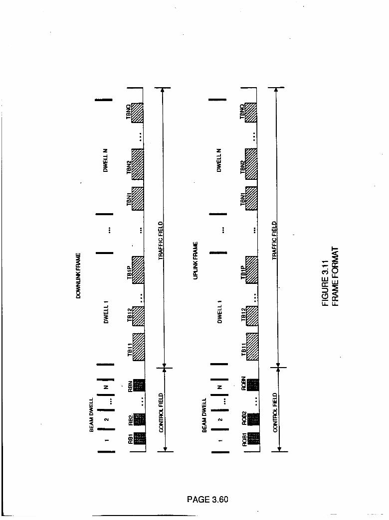
m
m
IJJ
m
Z
m
,.JW •
m
?,
t_
I
it
m
I,$.1
m
w
it
n
t,,I,
IJ.U_
PAGE 3.60
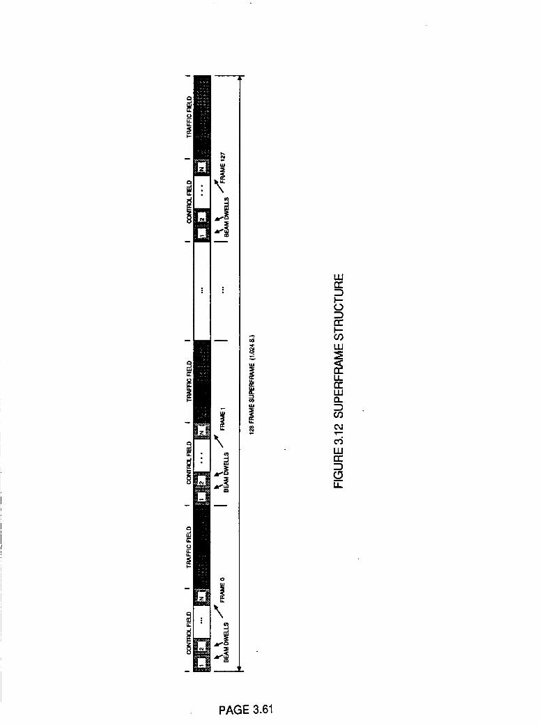
_v
w'5
a,.
ILl
uJn"
I.-
n-"I..-
uJ
u..EELUt'l
I.U
I..I.
PAGE 3.61
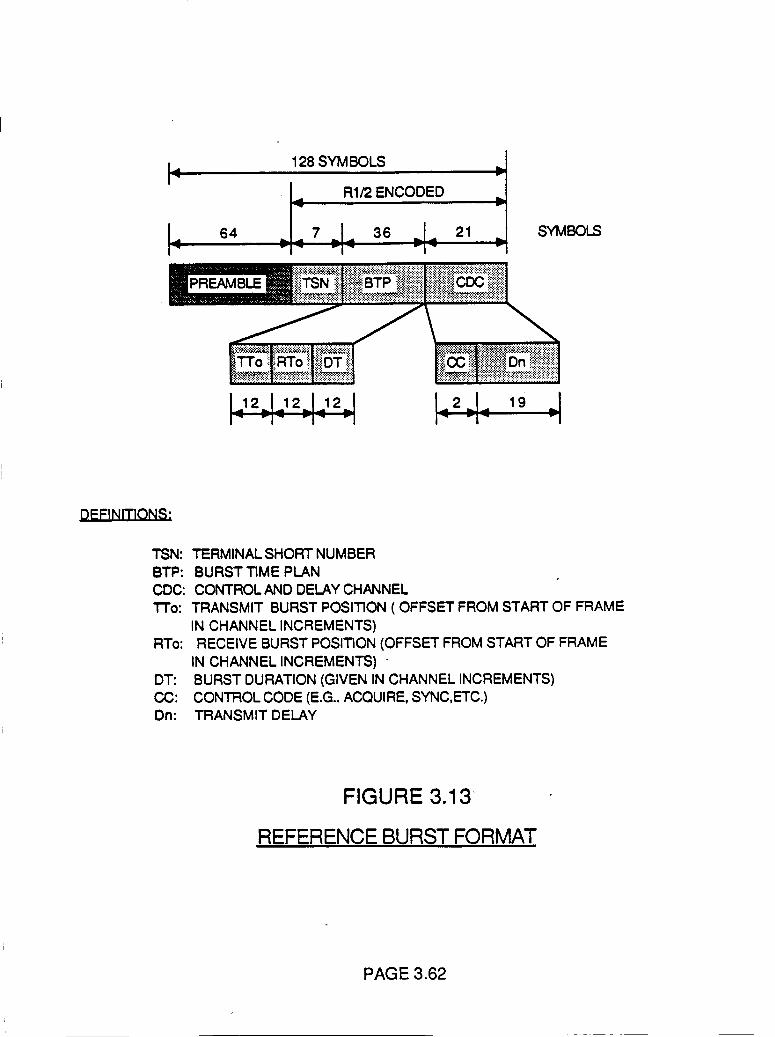
I-,, 128 SYM BOLS ,,.IT v
b, R1/2 ENCODED
_PREAMBLE liB::: TSN i,L::_.:::BTP:.;:_;_:.._;;,.:::iI::_::::;_CDC:._......:_::: ':- _..¢._' x;::::::_:: _:::::::b_, ' :::::._:• - ___Z'___::::::_:_:_::::::::::::::::::::::::::::::::::::::::::::::::::::::..............
_-_*_:_1_;_.;-;_;_;._I__:_m_'_a_i_l__.:;.| i__iiii:_ T _!__; _ • ;__:_:_:_:_::.__:_
-t_ -I_ "1 I _ -I- -
TSN:
BTP:CDC:
TTo:
RTo:
DT:CC:Dn:
TERMINAL SHORT NUMBERBURST TIME PLAN
CONTROL AND DELAY CHANNEL
TRANSMIT BURST POSITION ( OFFSET FROM START OF FRAME
IN CHANNEL INCREMENTS)RECEIVE BURST POSITION (OFFSET FROM START OF FRAME
IN CHANNEL INCREMENTS) "
BURST DURATION (GIVEN IN CHANNEL INCREMENTS)CONTROL CODE (E.G.. ACQUIRE, SYNC,ETC.)TRANSMIT DELAY
FIGURE 3.13
REFERENCE BURST FORMAT
PAGE 3.62
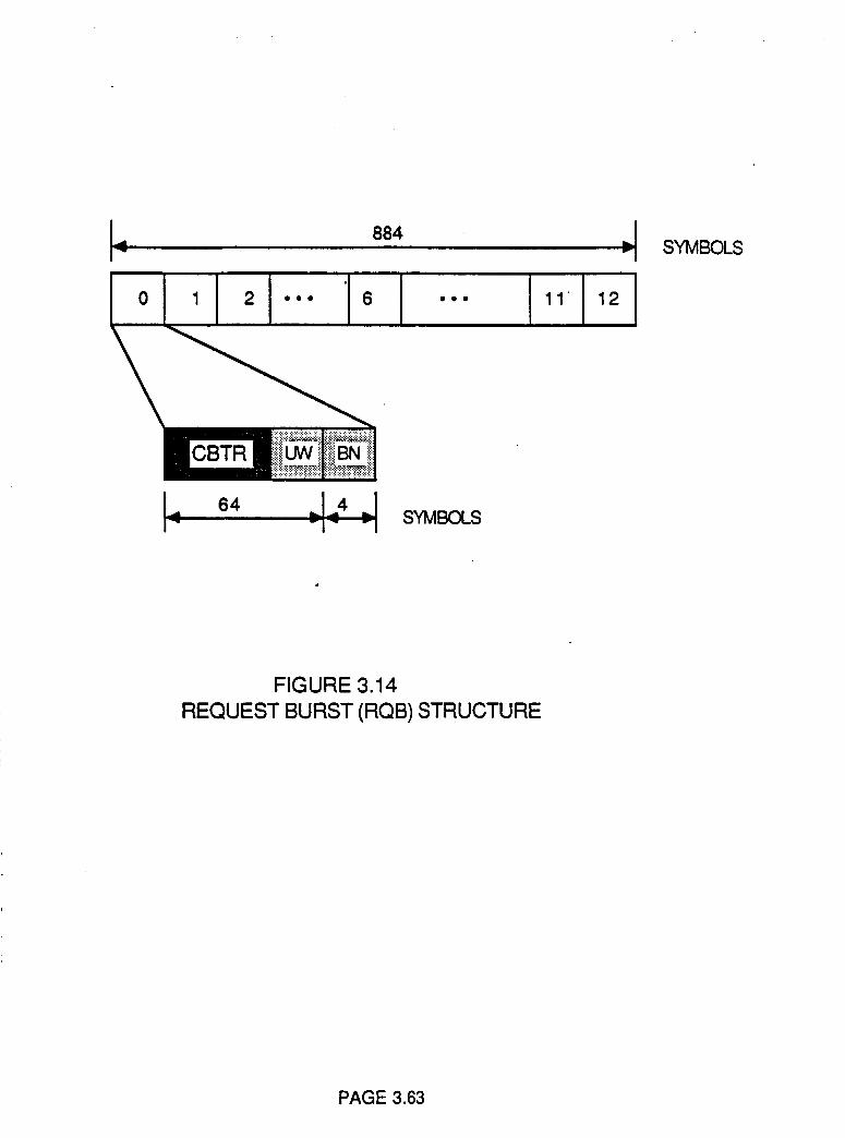
SYMBOLS
SYMBOLS
FIGURE 3.14
REQUEST BURST (RQB) STRUCTURE
PAGE 3.63

884 SYMBOLS d
68
SYMBOLSDWELL ACQUISITION
APERTURE (136 SYMBOLS)
FIGURE 3.15
RELATIONSHIP BETWEEN BEAM DWELL AND SUB-BURST
PAGE 3.64
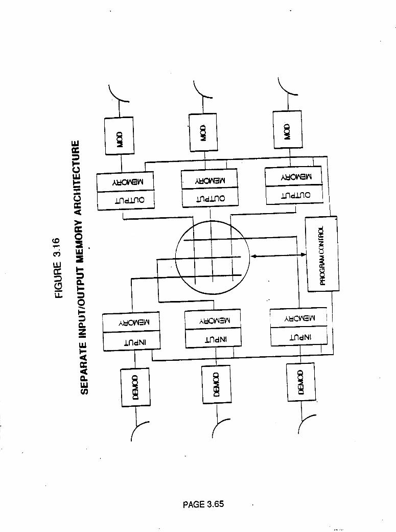
¢.o
rr::)
u..
I,I,I
I,I,I
0:iI,I,I
I-,
n_I-
0I,-=O.Z
CC
a._
.l.nclNl
PAGE 3.65
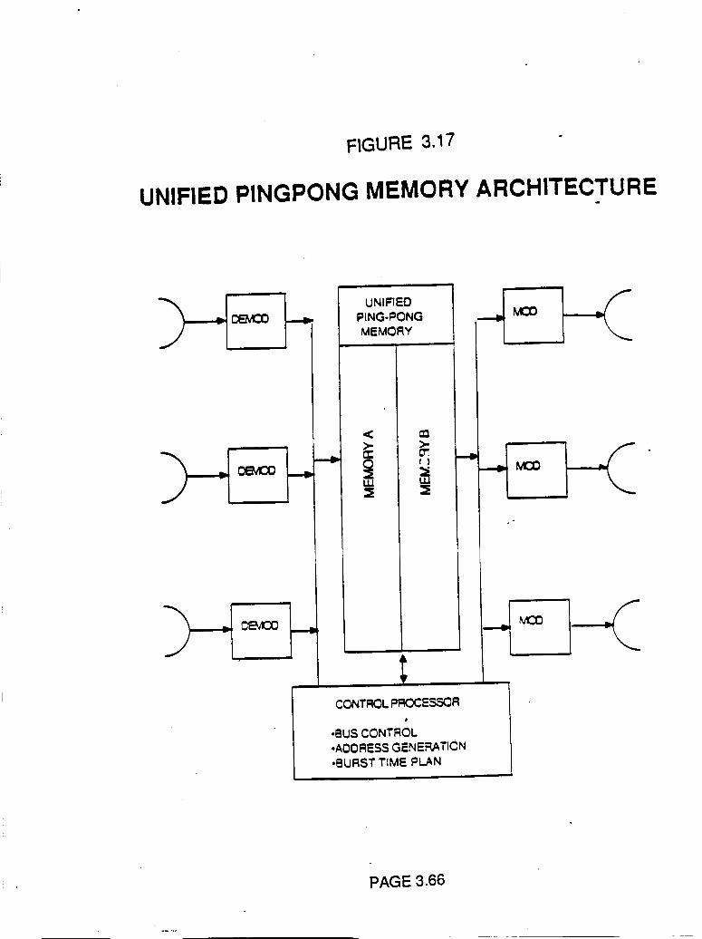
FIGURE 3.17
UNIFIED PINGPONG MEMORY ARCHITECTURE
CEM_
.<
UNIFIED
PING.PONG
MEM(_RY
CONTFIOL PRCCESSOR
0
•BUS CONTROL•AODRESS GENERATION
•6URST TIME PLAN
.°
MCO
MCO
PAGE 3.66
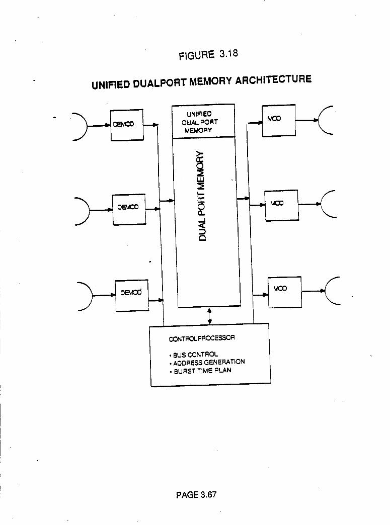
FIGURE 3.18
UNIFIED DUALPORT MEMORY ARCHITECTURE
N i
UNIFIED
OUAL PORT
MEMQRYi i
2
¢3
O3NTRCL PRCCESSCR
• 8US CONTROL
, AOORES$ GENERATICN
• BURST TIME PLAN
|1
i
PAGE 3.67
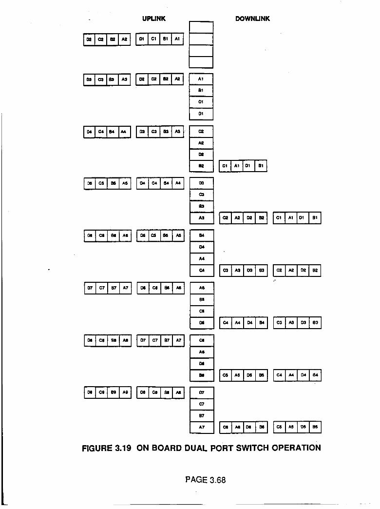
UPLINK OOWNUNK
1.1.1.1.11°,1°,1.,I.,I
I-I_1- I-I I_1_1-1-1
, I
, I
I
. !
A1
81
C1
01
I_lc'l" I"I1_1-1-1-1 . _' :
I_1-1- ,,11_.1_.1.1,.i
I_ -t-I"11-1-1-1-1
io,1o,1.,i,,11-1-1-1-1
----5Io'I"I°'I.,I
- I_'l-l-I-I I°'1"1°11''1
c, io1,1_1.1 i°1.1_,1.1A6
8S
. ic,l,,l_,l_l I°1_1_1-1i_1,1.1,.I I_1o1_,1,,I .
A6
M
I.I°.l..I-I I_l.l.l-i
87
RGURE3.19
I, I..I, I- I Ic.l..Io.1,.I
•, I-I,.I _.I..ION BOARD DUAL PORT SWITCH OPERATION
PAGE 3.68
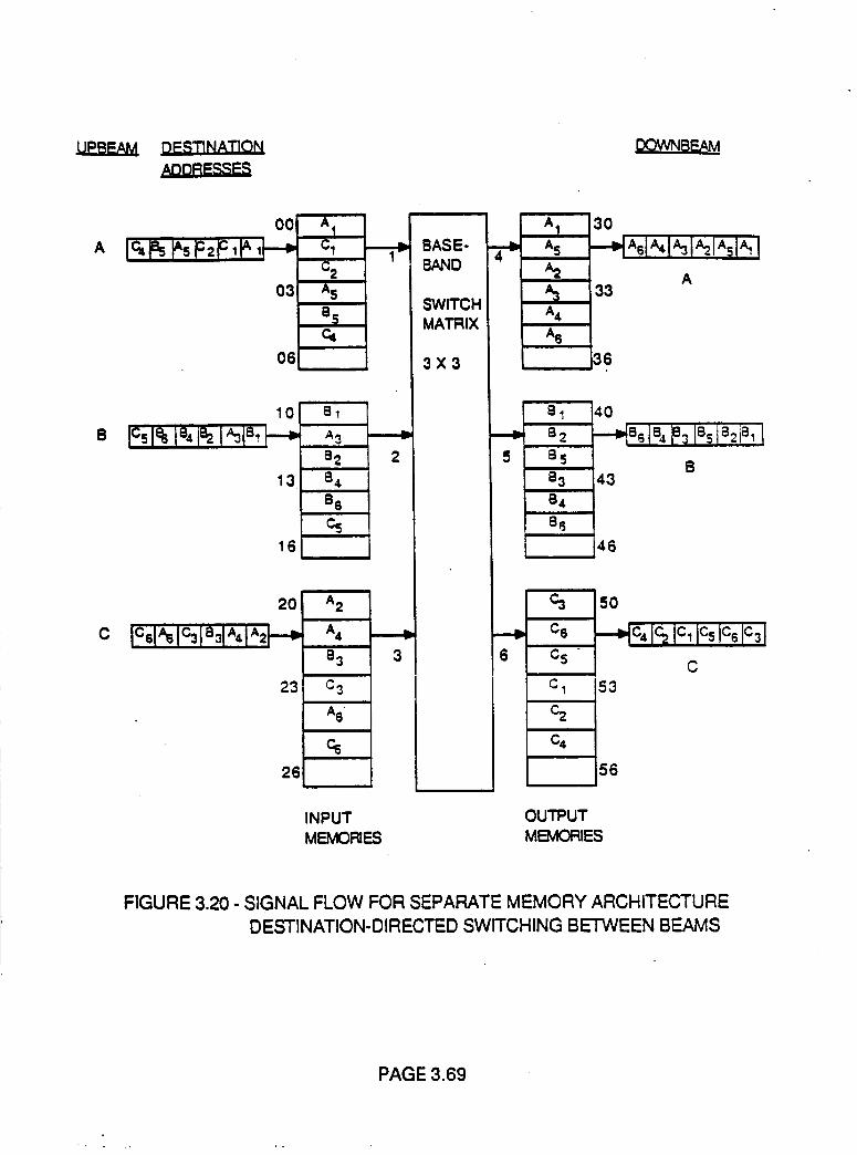
A
B
C
00
I_!_ I'_p2p,t,,I_
03
O6
lo;
13
16
2O
23
26
A1 i
C2
A5
B5C_
gl
A 3.
82 2
84
B6
csI
A2
A4
B3 3
C3
As
C6
i
INPUT
MEMORIES
BASE-BAND
SWITCHMATRIX
3X3
5
A 1
A5
A4
A6
30
---_A61A,I'_I_I*_IA,IA
33
36
81
g2
g5
B3
B4
gS
4O
B43
46
C3
CS
C5 -
C 1
C2
C4
53
56
OUTPUTMEMORIES
FIGURE 3.20 - SIGNAL FLOW FOR SEPARATE MEMORY ARCHITECTURE
DESTINATION-DIRECTED SWITCHING BETWEEN BEAMS
PAGE 3.69
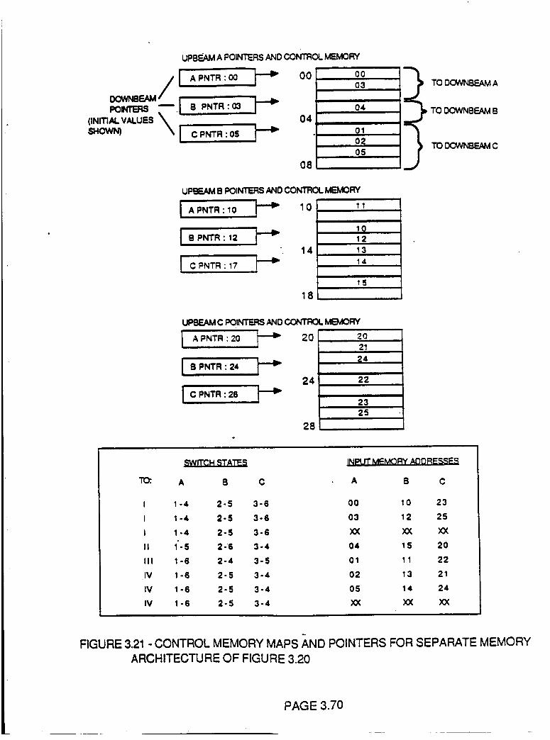
UPBEAM A POINTERSAND coNTRoL MEMORY
(JNm_W.UES
SHOWN) \ J
A PNTR : 00 _" 00
B PNTR : 03 _"04
C PNTR : 05 _"
O8
04
02
05
UpBEAM B POINTERS AND CONTRCI. MEMORY
J APNTR:10 _ 10 11
I B PNTR : 121012
14 1314
15
18
UI:_.AM C F_3_'ERS AND _ MEMORY
I APNTR:20 _' 20 2021
J BPNTR:24 _ _4
24 22
J CPNTR:2S _ 23
25
28
TO 0CWNBEAM A
TO O(:_'VNBEAMB
TO IXM/NBEAMC
=_I_._J_L._.T._,,_ INPUT MEMORY AOORESSES
TO:. A B C A B C
I 1 -4 2-5 3-6 00 10 23
I 1 -4 2-5 3-6 03 12 25
I 1 -4 2-5 3-6 _( _( XX
II 1"-5 2-6 3-4 04 15 20
III 1-6 2-4 3-5 01 11 22
IV 1 -6 2-5 3-4 02 13 21
IV 1 o6 2-5 3-4 05 14 24
IV 1 -6 2-5 3-4 _( ;_ XX
FIGURE 3.21 - CONTROL MEMORY MAPS AND POINTERS FOR SEPARATE MEMORY
ARCHITECTURE OF FIGURE 3.20
PAGE 3.70
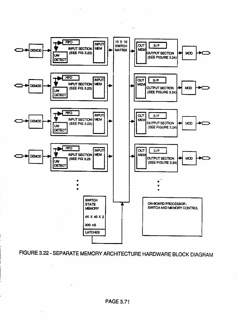
+23Dt+ P+t_._]_._ _ INPUT SECTION
- [---_ - I _ (SEE FIG 3.23)
_Nput_c_on 1mere1
(SEE FIG 3.23) U
/
10 X 10 /s_ I_i:--i-+_-----il_r_-l._! IOUTPUTSECmON_ m_O
L._.j tsEmmGUmma.,+,I I____.I
"_ _ CUTPUT SEGT1CN
/u+°+_+'l' '
<_ " INPUT SECTI<_
(SEE FIG 3.23
SWITCHSTATEMEMCRY
4KX40X2
300 nS
LATCHES
I
&
++
IN
ON-BOARD PROCESSOR -SWITCH AND MEMORY CCNTROL
FIGURE 3.22 - SEPARATE MEMORY ARCHITECTURE HARDWARE BLOCK DIAGRAM
PAGE 3.71
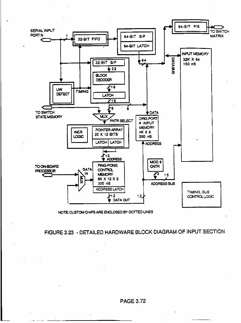
SERIAL INPUTPORTN
32-BIT FIFO64-BIT SIP
64.BIT LATCH
iTO SWITCH
DETECT
STATE MEMCRY
41NGLATCH
• 8
PCINTER ARRAYI INCR II I.CGIC I 20 X 13 BITS
I I
0ATA
;T I ORIG# INPUTl MEMORY
4KX8300 nS
TO (3N-BOARDR=E:X:;ESS_
<_
'13AOORES5
PING-PONG __.
8KX 12X2 • " .300 nS ADORES8 BLJS
LATCH I
12 120ATA OUT
64-BIT PIS
TO SWITCHMATRIX
INPUT MEMORY
32K X 64150 nS
NO'I'E:CUSTCM CHIPS ARE E_NCLOSEDBY DOT'rED lINES
.-II
TIMING, 8USCCNTRCL LCGIC
FIGURE 3.23 - DETAILED HARDWARE BLOCK DIAGRAM OF INPUT SECTION
PAGE 3.72
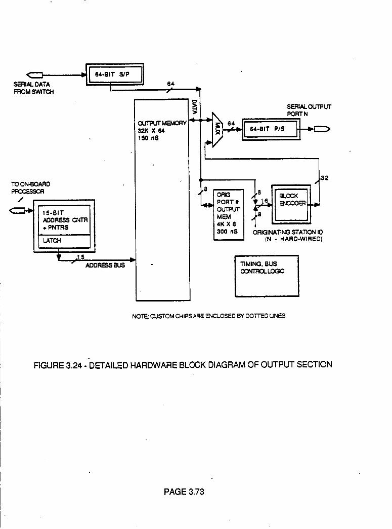
CSERIAL DATAFROM SWITCH
64
SERIAL OUTPUTPORTN
64-BIT P/S
ORGPORTOUTPUTMEM4KX8300 nS ORIGINATING STATION IO
(N - HARD-WIRE0)
I TIMING; BUS
CC_F_LCGIC
i
NO]E: CUSTQM CHIPS ARE _NCLGSED BY OCTI'ED LINES
FIGURE 3.24. - DETAILED HARDWARE BLOCK DIAGRAM OF OUTPUT SECTION
PAGE 3.73
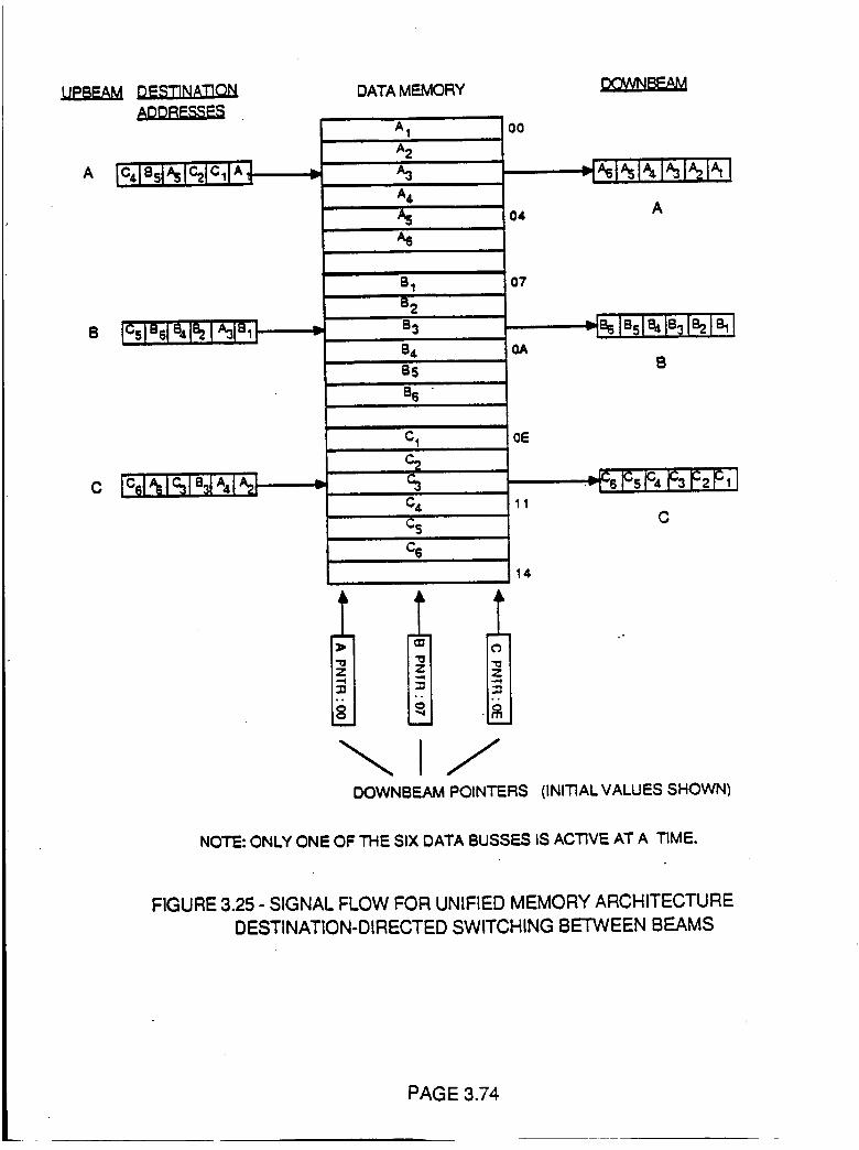
A
DATA MEMORY
A 1t
A2
00
04 A
B
C
B1
B2
B3
B4
85
86
C6
07
0A
0E
11
14
DOWNBEAM POINTERS
B
(INITIAL VALUES SHOWN)
NOTE: ONLY ONE OF THE SiX DATA BUSSES IS ACTIVE AT A TIME.
FIGURE 3.25 - SIGNAL FLOW FOR UNIFIED MEMORY ARCHITECTURE
DESTINATION-DIRECTED SWITCHING BETWEEN BEAMS
PAGE 3.74
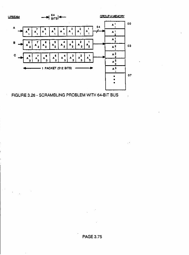
64B,Tsl+'"
A II
AI
A13
A 2I
A 2
A 23
A31
L '! '! 1 I 'I 11 11 11'1"
.d.,., '1'l '1 '1'I "
C 1 PACKET (512 BITS)
00
03
O7
FIGURE 3.26 - SCRAMBLING PROBLEM WITH 64-BIT BUS
PAGE 3.75
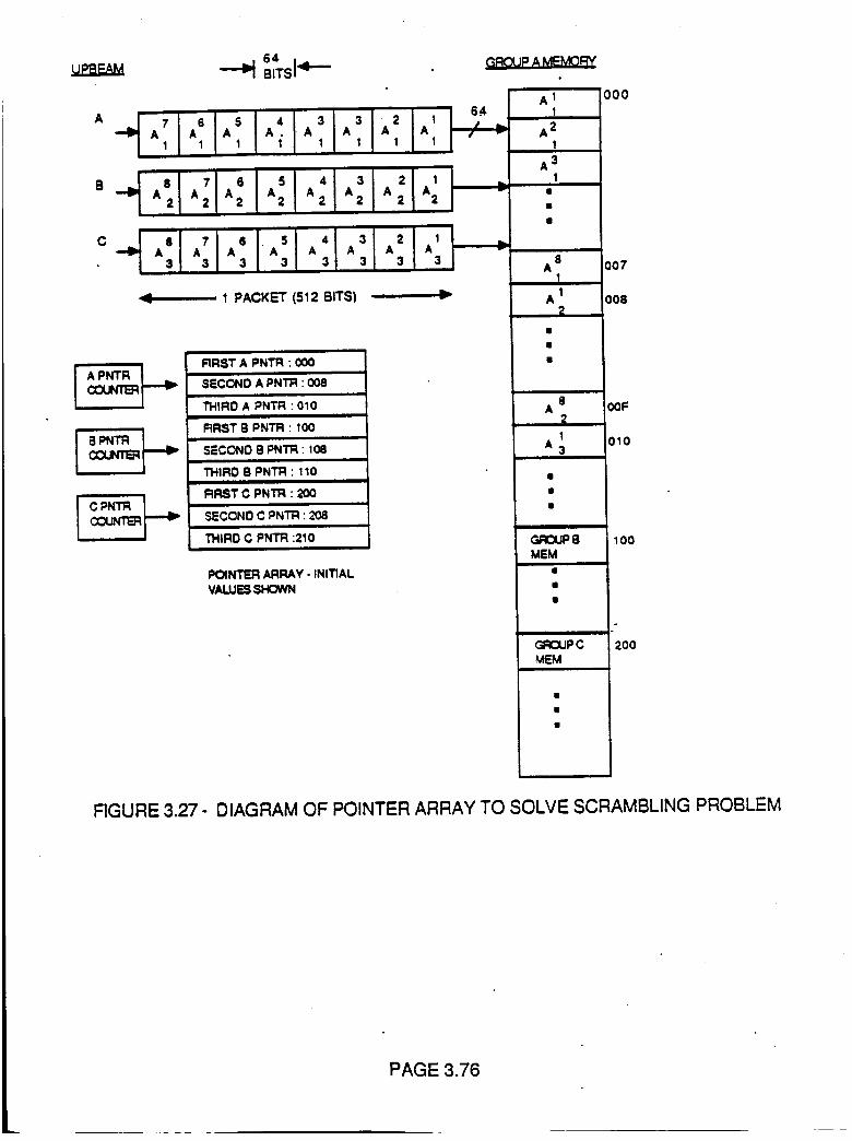
UPS_M64
--+t B,TSI4--
i,, i,,i1 I 1 1 I I,l
_l 8 i 7'l' 1 5 I "4 i A23 I A 22 ( I i
AS A6 .AS 4A A A 3 3/ 31 31 31 91 3 3
< 1 PACKET (512 BITS)
I APNTR I ,.-C:Ct._ j_._ ! -
I ap._ I .-
FIRST A PNTR : 000
SECONO A PNTR : 008
THIRD A PNTR : 010
FIRST S PNTR : 100
SECONO S PNTR" 108
THIR0 B PNTR : 110
FIRST C PNTR : 200
SECCN0 C PNTR : 208
THIRD C PNTR :210/
I:_NTER ARRAY - INITIALVALUES SHOWN
6.4
/
w
A 11
A 21
A 31
8A
I
IAz
8A
1A 3
GR3JP SMEM
, i 000
007
008
00F
010
100
o
200
FIGURE 3.27- DIAGRAM OF POINTER ARRAY TO SOLVE SCRAMBLING PROBLEM
PAGE 3.76
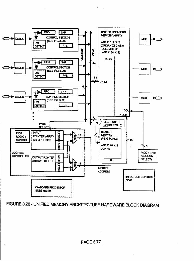
i
--E:: -[_,s,,,o_.)
_SECTION 64
T cocrR_ sEc_cN(SEE FIG 3.29)
P/$
I_,RLOGIC+
ADDRESS
ARRAY 10 X 16 _,_ [1_16
iii iii ii i i i IN
....,UBSYSTEM
UNIRED PING..PE_GMEMORY ARRAY
40K X 512 X 2
(ORGANIZED AS 8CO.U_IS CF
40K X 64 X 2)
25 n,S
"DATA
I'r _ 8t
COt
ADDR,d
8-BIT CNTR { '
I(ORIG $TN ID)
HEADERMEMCRY
16(PING-PONG)
40KX 16X22OO nS
tHFJkDER
ADDRESS
#16
_,3
I moo8cnTR4
I (COLUMNSELECT)
ii i i
FIGURE 3.28 - UNIFIED MEMORY ARCHITECTURE HARDWARE BLOCK DIAGRAM
PAGE 3.77
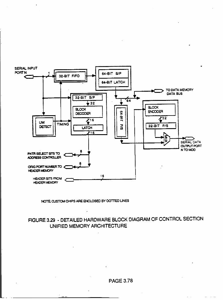
SERIAL INPUTPORTN
1
I
I
D_'-=CT 41NG
i
ii i
I,_-_'__ I_32
I BLCCX0ECCOER
I LATCH_'16
PNTR SELECTBITSTO " '_D_SS_
OR_ _ NUMBERTOHEAOERMEMCRY
16_OE_ aTsaM C /HEADERMEMORY
TO DATAMEMORYDATA BUS
_ -_;_
SERIAL DATAOUTPUTPORTNTO MOO
NOTE: CUSTOM CHIPS ARE ENCLOSED BY OOTFED LINES
FIGURE 3.29 - DETAILED HARDWARE BLOCK DIAGRAM OF CONTROL SECTION
UNIFIED MEMORY ARCHITECTURE
PAGE 3.78
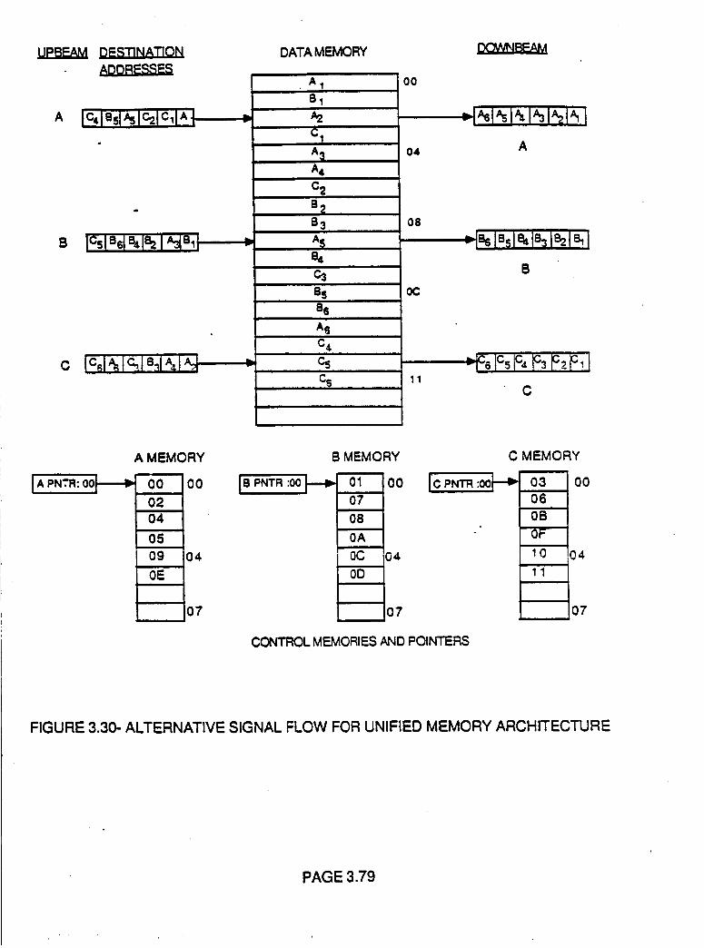
B
C
DATA MEMORY
A 1
B1
00
O4
0C
11
A
B
A MEMORY
I A I=N,'R: 001_. O0 0002
04
05
09 04
0Eii
B MEMORY
18_NrR:oo_ 'oI Ioo!
O8 I
0A I
_ 104
Ioo I!
07 ' '07l I
C MEMORY
Ic,'_'. :oo1-_03 Iooo6 1os I
OF II
10 104
i"" to,CONTROL MEMORIES AND POINTERS
FIGURE 3.30- ALTERNATIVE SIGNAL FLOW FOR UNIFIED MEMORY ARCHITECTURE
PAGE 3.79
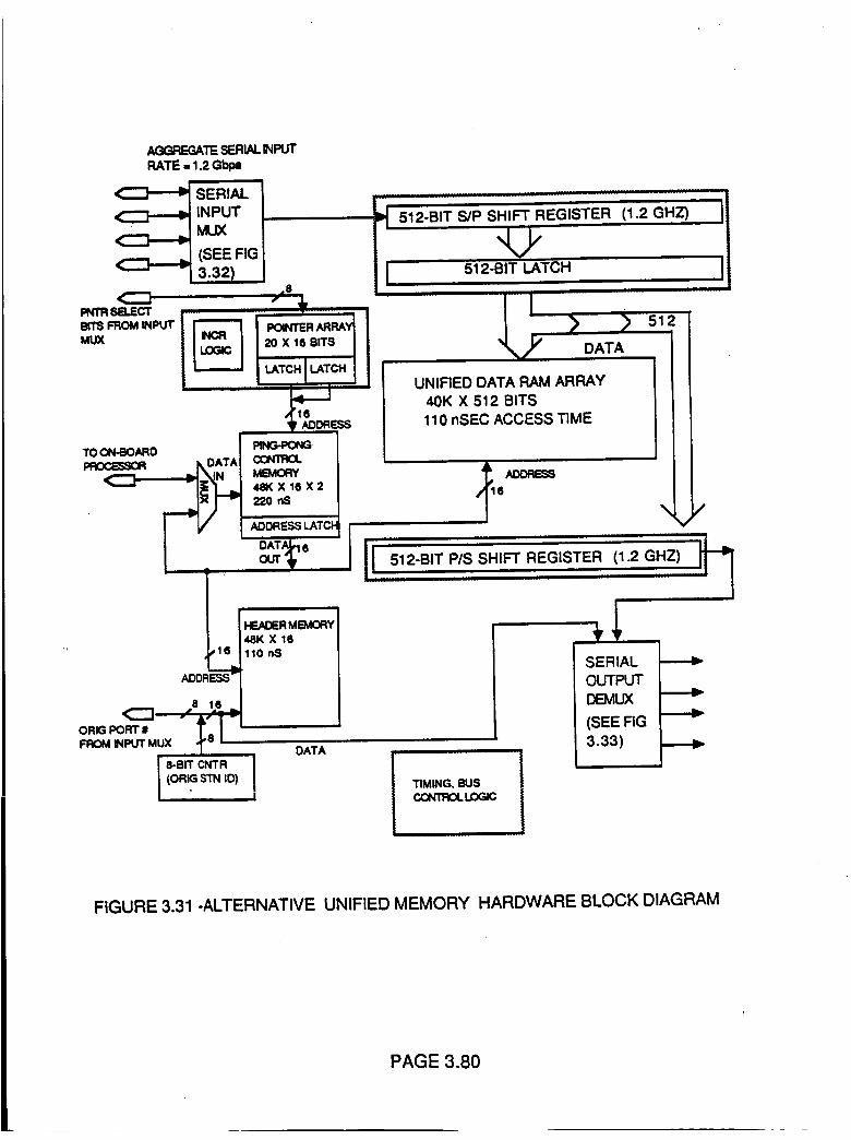
A_EGATE SERIALINPUTRATE ,, 1.2 Glm=
SERIAL
INPUT
MUX
(SEE FIG3.32)
16
ADDRE_"!1
TOON-BOARD
<__8 16ORIGPORT# T_I
FROMINPUTMUX _ n
I 8-BIT CNTR(ORIGSTNID)
I
OUT'
PLEADERMBAORY48K X 16110 nS
DATA
512-BIT S/P SHIFT REGISTER
512-BIT LATCHi
DATA
(1.2 GHZ) I
UNIFIED DATA RAM ARRAY
40K X 512 BITS
110 nSEC ACCESS TIME
512
512-BIT P/S SHIFT REGISTER (1.2 GHZ)
J TIMING. BUS
I CCNTROLLOG_
SERIAL
OUTPUTDEMUX
(SEE FIG3.33)
!!
n Hi _
I nl
FIGURE 3.31 -ALTERNATIVE UNIFIED MEMORY HARDWARE BLOCK DIAGRAM
PAGE 3.80
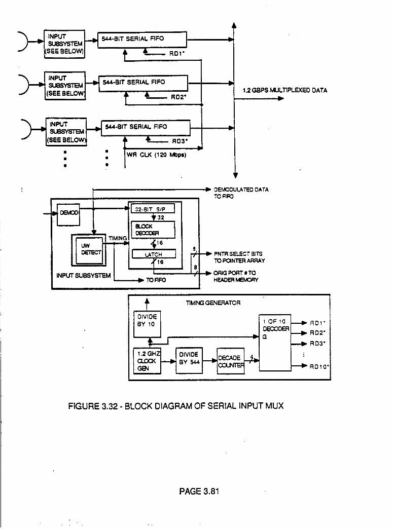
_S INPUT L_J
sussYs_i-_ IEE BELOW)_
544-BIT SERIAL FIFO 'i
f & R01"
INPUT I =JSI_ [_3 544-BIT SERIAL FiFO v
1.2 GBPS MULTIPLEXED 0ATA
v
0EMOOULATED0ATATO FIFO
PNTRSELECTBITSTOIK_NTER ARRAY
ORIG IM:_RT= TOHEADERMEMORY
fI0,v,o I
BY10 I
TIM_G GENERATOR
v
1 OF100ECX:)0ER
G
R01"
RO2"
R03"
RD10'
FIGURE 3.32 - BLOCK DIAGRAM OF SERIAL INPUT MUX
PAGE 3.81
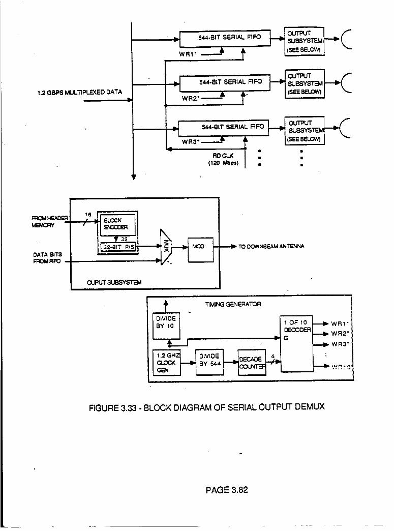
_E. 544-BIT SERIAL FIFO
WRy-
1.2 GBPS MULTIPLEXED 0ATAWR2
544-BIT SERIAL RFO¢UTI=UTSUBSYSTEM
(SEEBELOW)
544-81T SERIAL FIFO
WR3"
RD CLK •(120 Mbp$) •
DATA BITSFF¢_ RFO
32-BIT _/S TO CX3WNBEAMANTENNA
CXJPUTSUBSYSTEM
tOIvIIBY 1
13MINGGENERATOR
Lv
CLCX BY 544_,
==" I I I I....... I I
1 OF10OECOOER
G
WR1"
WR2"
WR3"
vv_ltI
FIGURE 3.33 - BLOCK DIAGRAM OF SERIAL OUTPUT DEMUX
PAGE 3.82
NAS3-24886 FINAL REPORT
4.0 INTEGRATION OF OTHER SERVICES
The integration of services other than the trunk telecommunications
and data services may be accomplished with only minor extension of theonboard architecture discussed in section 3. Two additional services to be
examined are the Mobile and Intersatellite Link Services. These will be
addressed in the following sections.
4.1 MOBILE SATELLITE SERVICE
Two methods for accommodating the transmission of the destination
addressed packets have been described in the foregoing, viz., packet
routing and sub-burst routing. Packet routing is the most suitable for thin
route terminals using very small antennas such as would be desirable for
mobile communications to sea, land and airborne platforms. In such cases,
the packets would be carried on low bit rate continuous FDMA carriers that
are not shared in the time domain and would be supported in a fixed beam
covering a whole area such as CONUS. This would result in the most power
efficient earth terminal, a property important for power limited mobile
communications. In contrast the destination directed sub-burst method is
suitable for earth terminals carrying multiple channels such as those
needed for thin and medium capacity telephone trunks. These can operate
in a TDMA transmission format served by hopping beams. Onboard the
satellite, all channels, continuous and burst, would be routed at baseband
by the same destination directed switching machine. Using this approach,
the Mobile service can be directly interconnected to the public switched
telephone network. The following sections examine how thin-route mobile
service can be integrated into the destination directed on board
processing architecture. Attention will be focussed on the Land Mobile
Service, but the conclusions drawn are applicable to other mobile
services, i.e. maritime and air mobile and other thin route services such
CPS business and DAMA telephony.
4.1.1. INTEGRATED FIXED SATELLITE AND LAND MOBILE SATELLITE SERVICES
The subject of a land-mobile satellite system has been studied in
extensive detail [11- 14 ] in which numerous tradeoffs have been
performed which lead to a possible system architecture. Drawing upon the
results of the these studies, a system that utilizes a multiple-access
scheme similar to that which was developed for the Mobile satellite
PAGE4.1
NAS3-24886 FINAL REPORT
Experiment (MSAT-X) is examined. Since the MSAT-X system does not
incorporate on board processing, some modification to the original conceptis needed.
The basic network elements of a fully integrated Fixed Satellite
service (FSS) and Mobile Satellite Service (MSS) system are given in figure
4.1. The on-board packet processing satellite serves two basic types of
stations operating in the FSS, those which interconnect to the public
switched telephone network (PSTN) and those which are located on the
customer's premises (CPS). The transmission link for this service is at
K-band and utilizes hopping beams.
The onboard processor also serves the mobile satellite service at
L-band or UHF. For mobile platform antenna design and transmission
reasons, UHF band is preferred for mobile communications; however,
permission to use UHF in CONUS has not been granted. In this text, for
simplicity, mobile services are said to be at L-band. Fixed beams are
positioned over the service area which is assumed to be CONUS. The
on-board packet processor can serve mobile terminals (MTs) and base
stations (BSs) at L-band. Base stations can also be located at FSS K-band
stations where feeder links to the MSS occur. Thus, any MT can have direct
access into the PSTN by on-board packet routing the call through an
appropriate FSS gateway earth station operating at K-band. On rare
occasions, a base station operating at L-band might be encountered when a
MT transceiver is deployed at a base station. This requires MT toMT(serving as a BS) communications. The on-board processing
architecture being studied permits single-hop MT to MT communication.
4.1.2 SYSTEM CHARACTERISTICS
The mobile satellite channels are accessed in frequency rather than
time. Each channel is carried as a Single Channel Per Carrier (SCPC).
Because of link budget considerations, the nominal carrier bit rate and
channel bandwidth should be kept as low as practical. Narrow bandwidth is
also essential to packing a sufficient number of SCPC'carriers into the
very limited L-band spectrum assigned to the service. To accomplish
this, voice communications using low rate encoding is required. For the
system considered here it is assumed that voice will use 2500 bit/s low
rate source coding and this will be rate 1/2 FEC coded to yield a traffic
channel rate of 5000 bit/s. The capacity needed to carry the destination
address information must be added to get the total channel rate. The total
channel rate is a function of the TDMA frame period and the channel
bandwidth a function of the TDMA frame period and the modulation
PAGE42
NAS3-24886 FINAL REPORT
technique. The total channel bit rate is 9000 bit/s for a 8ms frame period
and 7000 bit/s for the 16ms frame period. For TDMA frame periods of 8
and 16ms, using BPSK modulation the channel bandwidths are 12 and 9 kHz
and using QPSK modulation, the channel bandwidths are 6kHz and 4.5kHz
respectively. Separate request channels are used by the MTs to gain
access to the satellite and a separate status and signalling channel is
received by all MTs that desire to receive incoming calls.
Typical uplink and downlink frequency plans are shown in figure 4.2. A
"Channel Request" is made by a MT using a slotted Aloha random access
method. The request channel frequency is also selected on a random basis
by the MT. Since the frequency boundary between the request and
information channels dynamically changes depending on the relative
instantaneous loading between the two sets of channels, the MTs must be
informed of the boundary location between the request channels and the
transmit information channels. This information is conveyed over thestatus and timing channel to which all the MTs listen. This channel also
provides the timing markers for slotted Aloha transmissions. If desired,
the MTs can scan the active signaliing channels to receive incoming calls.
4.2 CALL SET-UP PROCEDURES
Three basic types of call set-up procedures are needed in this system:
1. Call originating at MT and destined to BS or gateway in FSS,
2. Call originating from BS or gateway in FSS and destined to MT,
3. Call from MT and destined to MT which may be a MT transceiver
operating at 1-band and serving as a BS.
4.2.1 Calls Originating at MT to BS or Gateway
The call set-up procedure for calls originating at a MT and destined to
either a BS or FSS gateway station is as follows:
• MT sends a request message (RQM) over a request channel usingslotted Aloha.
• The on-board packet processor (OBPP) assigns a channel comprisinga frequency pair (transmit/receive) from the pool of information channels
to the requesting MT.
• The MT either receives a frequency pair of channels within a
specified period of time or assumes that its request was not received by
the OBPP because of packet collision.
• If the MT receives the satellite channels it proceeds as normal by
sending a call set-up message (CSM) packet in an identical manner to that
used for the FSS. These procedures are described in Section 3.1.
PAGE4.3
NAS3-24886 FINAL REPORT
• If the MT does not receive the pair of channels, it continues to send
request messages in a random fashion until it receives a pair of channels.
4.2.2 Calls Originating at BS or Gateway to MT
The call set-up procedure for a call originating at a BS or Gateway
station in the FSS with a MT destination is as follows:
• BS or FSS places a call in the conventional manner using a CSM in
one of its assigned satellite channels (time slots).• The OBPP reads the header and determines that the destination is a
MT as indicated by its destination address.
• The OBPP signals the called MT of an incoming call and assigns the
frequency pair of channels over which the call will be carried. This
information is conveyed over one of the signalling channels that is
currently in use.
• The MT tunes to the assigned channel pair.
• The OBPP sends the CSM over the assigned channel pair.
• Normal packet flow, as described in Section 3.1, continues until the
call is terminated.
• Upon call termination, the frequency pair is returned to the pool of
unused frequencies and is available for use on another call.
4.2.3 Calls Originating at a MT Destined to a MT
The call set-up procedure for calls originating at a MT and destined to
another MT is a combination of the above two procedures and is as follows:
• MT sends a request message (RQM) over the request ct_annel usingslotted Aloha.
• The OBPP assigns an information channel to the requesting channel.
• Once that the originating MT has successfully obtained a pair of
information channels, it proceeds as normal by sending a CSM packet.
• The OBPP reads the header and determines that the destination is a
MT as indicated by its destination address.
• The OBPP signals the called MT of as incoming call and assigns a
pair of frequencies over which the call will be carried. This information
is conveyed over one of the signalling channels that is currently active.
• The MT tunes to the assigned pair of information channels.• The OBPP sends the CSM to the called MT over the allocated channel
pair.
• Normal packet flow continues, according to the procedures
described in Section 3.1, until the call is terminated.
• Upon call termination, the two channel pairs are placed back into
PAGE4.4
NAS3-24886 FINAL REPORT
the pool of unassigned frequencies and are available for use on another
call.
4.3 IMPACT ON THE ON-BOARD PACKET PROCESSOR
"4.3.1 INTEGRATION OF FSS AND LMSS
A block diagram of the onboard packet processor that provides
integrated FSS and MSS is given in Figure 4.3. The L-band fixed beams, the
L-band receiver and HPA are RF components that need to be added to the
original design concepL The demods and mods are all SCPC and operate at
at low bit rates in a frequency division multiple access (FDMA) mode. The
outputs of the SCPC demods are aggregated in a time division multiplexer
which translates the frequency multiplexed satellite channels into time
multiplexed satellite channels. Because the MSS channels operate at lower
bit rates than the FSS channels it is necessary to add dummy bits within
the traffic portion of each packet when going from MSS to FSS channels
and remove dummy bits when going from FSS to MSS channels. Once this is
done, the MT (MSS) information channels are indistinguishable from those
of the FSS and can be treated by the OBPP without special consideration.
The demods, which are allocated to the request channels and roods which
are allocated to the status and signalling channels, must be treated
separately since they are not handling the normal packets.
At the output of the OBPP, the TDM information channels are
_i ,l÷i I..,emu,,,p,exed and the time slot channels are translated into frequency
slot channels. This is accomplished by arranging the time slots in the
OBPP in a way that the demuitiplexed channels will occur at the input to
the modulator having the proper output frequency and at the low FEC coded
bit rate of the MT channels. This is carried out by the OBPP in the same
way that it handles all other packets, i.e. it routes packets into their
proper time slots. Since the OBPP operates only on the packet headers, MSS
information packets are indistinguishable from the FSS packets and are
handled identically. The packets associated with request, status or
signalling are handled separately.
4.3.2 MSS IMPLEMENTATION
Figure 4.4 is a block diagram of the additional implementation needed
to incorporate the MSS. The aggregate information rate presented to the
MSS processor to handle the request, status and signalling packets for
assignment of the MSS carriers is very low, on the order of 10 kHz. The
PAGE4.5
NAS3-24886 FINAL REPORT
speed of the associated processor memory is essentially determined by
this aggregate rate. The exact speed depends on the maximum number of
request channels that are to be accommodated. The power requirements
and complexity of this processor are expected to be small compared to the
OBPP. The multiplier and demultiplexer needs to provide a dynamic
boundary to accommodate changing the ratio between the information
channels and the request channels and the status and signalling channels.
The dynamic boundary in the multiplexer is used to segregate request
channels destined to the MSS processor from the MSS information
channels that are destined to the OBPP. In the demultiplexer, the dynamic
boundary combines the status and signalling channels provided by the MSS
processor with the MSS information channels provided by the OBPP.
4.3.3 DIFFERENCE IN TRAFFIC BIT RATES OF MSS/FSS LINKS
The system must provide a means to cross connect MSS and FSS linksand to accommodate the difference in traffic bit rates. A means for
accomplishing this is now discussed.
MSS will incorporate low bit rate voice coding to carry voice
messages. The MSS channels should operate at a transmission rate that is
an integer submultiple of 32 kbit/s so that each packet carries an even
number of bits. This must be done so that the MSS packets can be aligned
with the FSS packets in the onboard baseband processor. In general, this
results in rates given by the relation 2n/T F where T F is the TDMA frame
period and n= 1, 2, 3 ........... This choice is based on carrying 2 bits per
symbol using QPSK and does not prohibit the use of BPSK on the LMSS links.
The resulting rates are integer multiples of 250 and 125 Hz for frame
periods of 8 and 16 ms respectively. This excludes rates such as 2400,
4800 and 9600 bit/s in favor of rates such as 2500, 5000 and 9750 bit/s.
MSS transmission would be in terms of a single channel per packet
with a frame duration equal to 8 or16 ms comprising a 32 bit, rate1/2
coded packet header and a traffic portion containing RcT F bits where Rc is
the coded channel bit rate. Thus, for a voice coder operating at 2500
bit/s, 40 or 80 coded traffic bits per packet would occur for the 8 or 16
ms frames respectively. To this would be appended the 32 bit destination
address header yielding a total length of 72 or 112 bits respectively which
require transmission bit rates of 9000 or 7000 bit/s respectively. Based
on a 30% guard band between SCPC MSS carriers, transmission channel
spacings of 12 kHz or 9kHz would result respectively using BPSK
PAGE4.6
NAS3-24886 FINAL REPORT
modulation or 6kHz or 4.5kHz using QPSK.
The MSS carriers would be demultiplexed and demodulated onboard to
baseband without decoding of the traffic. A digitally implemented onboard
multichannel demultiplexer/demodulator processor such as that studiedunder NASA LeRC contract NAS3- 24885 could be used for this function.
The packet headers would be processed in the same way as for FSS. The
traffic portion would be multiplexed onto a 32 kbit/s downlink carried in
the TDMA packet format. Since the transmission rate on the FSS channels
is much higher than on the MSS channels, less bits are used on the MSS
channels and the unused bits in the FSS packet would be dummies. It is up
to the processor in the earth station to demultiplex the MSS channel bits
from the FSS packets and either transcode them to a standard telephone
system code such 32 kbit/s ADPCM or to convert them to analog voice or to
transport the low bit rate code to its destination where it is decoded.
Transmission in the reverse direction, i.e. FSS to MSS, is
accomplished by reversing the steps. The low bit rate MSS signal padded
with dummy bits is carried to the satellite on 32 kbit/s FSS uplink
packets where they are demodulated, demultiplexed, rate conversion
buffered and routed to the MSS downlink modem operating at the
appropriate downlink frequency.
4.3 INTERSATELLITE LINK OPERATION
Important factors regarding the implementation of the intersatetlite
link are now considered. From the networking point of view, it is
important to direct attention to the needs of the onboard intersatellite
link interface. The most important property of the intersatellite link
influencing the interface is variation in the path length between the
satellites. This problem is the same whether the link is a short or a longone. If the distance between satellites are held to a tolerance of +®
degrees, then the variation in distance can be as great as 9.90 ms max.
peak-to-peak. Thus, if the satellites are held to a tolerance of _-K).1
degrees, the path length can vary by 0.99ms max. peak-to-peak, but if the
tolerance increases to 1 degree the path length change increases to 9.9ms
max-peak to-peak. It is also possible to fly two satellites in formation to
decrease the max. peak-to-peak intersatellite path length variation, but
this increases position keeping fuelconsumption in the trade.
To be properly synchronized the digital signals on each satellite will
require buffering of the number of bits occupying the amount of time equal
PAGE4.7
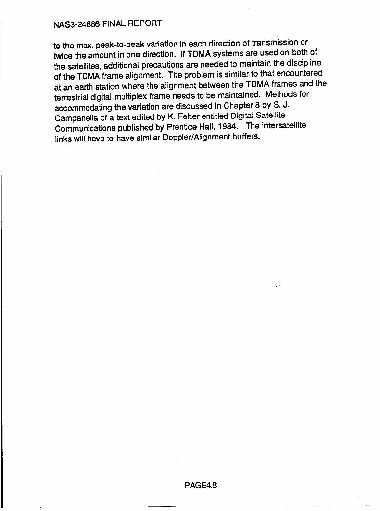
NAS3-24886 FINAL REPORT
to the max. peak-to-peak variation in each direction of transmission ortwice the amount in one direction. If TDMA systems are used on both of
the satellites, additional precautions are needed to maintain the discipline
of the TDMA frame alignment. The problem is similar to that encountered
at an earth station where the alignment between the TDMA frames and the
terrestrial digital multiplex frame needs to be maintained. Methods for
accommodating the variation are discussed in Chapter 8 by S. J.
Campanella of a text edited by K. Feher entitled Digital Satellite
Communications published by Prentice Hall, 1984. The intersatellite
links will have to have similar Doppler/Alignment buffers.
PAGE4.8
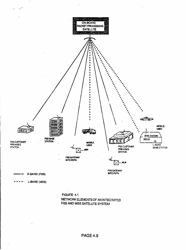
ON-BOARDPACKET PRCCESSING
SATELLITE
STATION
---- K-BAND (FSS)
..... L-BAND (MSS)
M_ILE1 LJ_R
icro I_"I'N
F_e,SGA'I'EWAYINTOPSTN
FIGURE 4.1
NETWORK FI EMENTS OF AN INTEG,%_,'I'ED
FSS AND MSS SATELLITE SYSTEM
PAGE 4.9
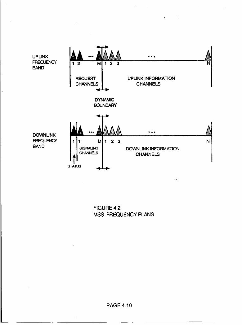
UPLINKFREQUENCY
BAND
DOWNIJNK
FFE-CLIENCY
BAND
DYNAMIC
BOUNDARY
"-r"
1 1 MI1 2 3
SIGNALING I
t CHANNELS I
STATUS
UPUNK INFORMATION
CHANNELS
DOWNLINK INFORMATION
CHANNELS
N
N
FIGURE 4.2
MSS FREQUENCY PLANS
PAGE 4.10
ORIGIN'ALPAGE IS
OF POORqU I
I
fiii!iiiiiii_
1
E LU
_,,=,LU ¢,/)
_') G. =d_ I"- O0
LULl-
,';'ar,.._
OU.
PAGE 4.11
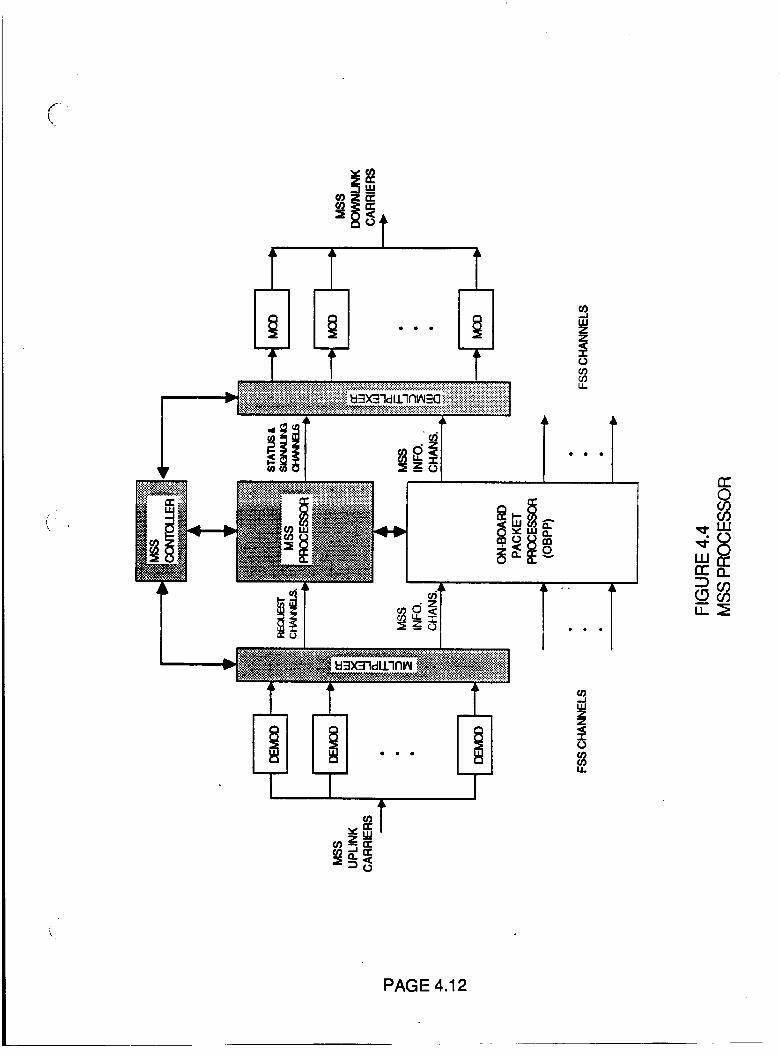
I
E;
[] [] ...[]
iil
I!"
";"";.........._ :;:i,2;,'.;;;;_l=l=lX--J7dl17nl_l_ @_l,:l"$'.'$'.1:
0¢0¢0U.
_ oL
,i.JILlZZ
i t
r_
_W
_09
PAGE 4.12
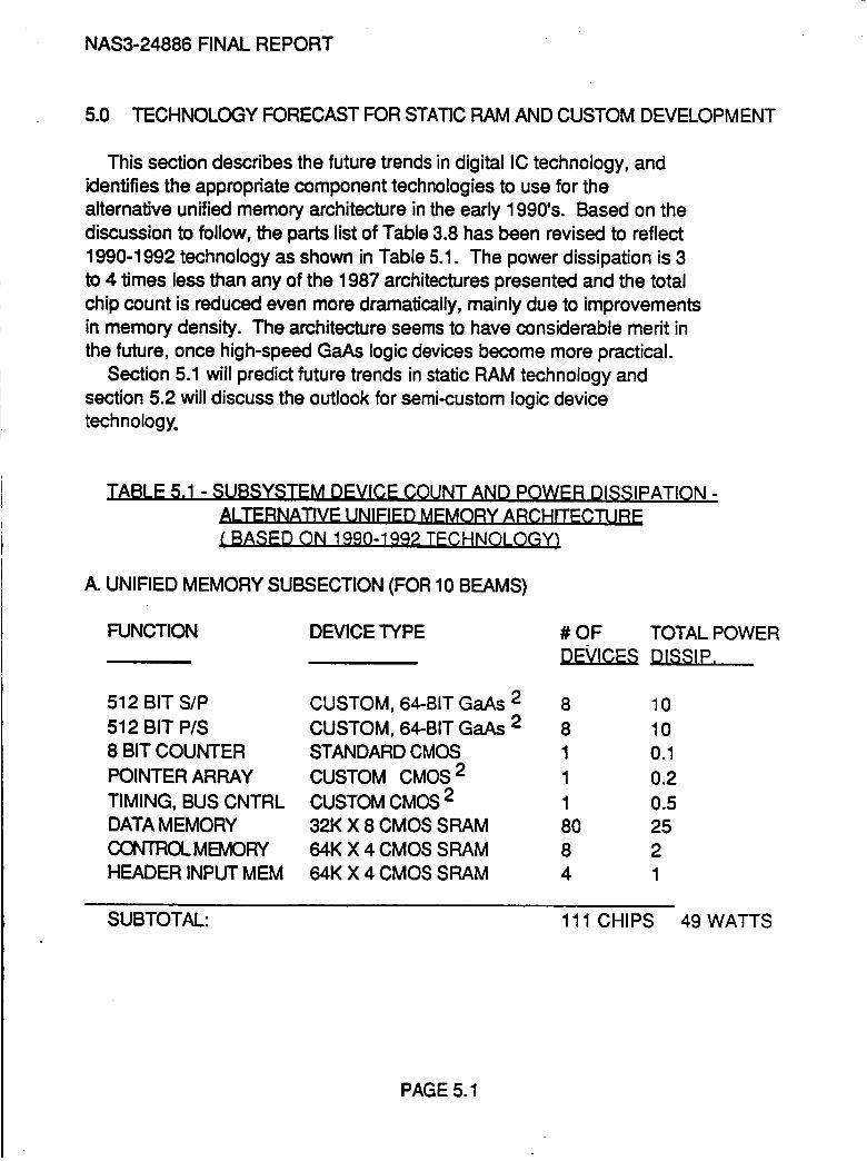
NAS3-24886 FINAL REPORT
5.0 TECHNOLOGY FORECAST FOR STATIC RAM AND CUSTOM DEVELOPMENT
This section describes the future trends in digital IC technology, and
identifies the appropriate component technologies to use for the
alternative unified memory architecture in the early 1990's. Based on the
discussion to follow, the parts list of Table 3.8 has been revised to reflect
1990-1992 technology as shown in Table 5.1. The power dissipation is 3
to 4 times less than any of the 1987 architectures presented and the total
chip count is reduced even more dramatically, mainly due to improvements
in memory density. The architecture seems to have considerable merit in
the future, once high-speed GaAs logic devices become more practical.
Section 5.1 will predict future trends in static RAM technology and
section 5.2 will discuss the outlook for semi-custom logic device
technology.
TABLE 5.1 - SUBSYSTEM DEVICE COUNT AND POWER DISSIPATION -
ALTERNATIVE UNIFIED MEMORY ARCHITECTURF
( BASED ON 1990-1992 TECHNOLOGY)
A. UNIFIED MEMORY SUBSECTION (FOR 10 BEAMS)
FUNCTION DEVICE TYPE # OF TOTAL POWER
DEVICES DISSIP.
512 BIT S/P
512 BIT P/S
8 BIT COUNTER
POINTER ARRAY
TIMING, BUS CNTRLDATA MEMORY
_OLMEMORY
HEADER INPUT MEM
CUSTOM, 64-BIT GaAs 2 8
CUSTOM, 64-BIT GaAs 2 8
STANDARD CMOS 1
CUSTOM CMOS 2 1
CUSTOM CMOS 2 1
32K X 8 CMOS SRAM 80
64K X 4 CMOS SRAM 8
64K X 4 CMOS SRAM 4
10
10
0.1
0.2
0.5
25
2
1
SUBTOTAL: 111 CHIPS 49 WATTS
PAGE 5.1

NAS3-24886 FINAL REPORT
B. INPUT MUX SUBSECTION (FOR 10 BEAMS)
FUNCTION
BLOCK DECODER
UW DETECTOR
TIMING GENERATOR
544 BIT FIFO
DEVICE TYPE # OF TOTAL POWER
DEVICES DISSIP.
CUSTOM 1 10 10
CUSTOM 1 10 10
CUSTOM GaAs 1 1
CUSTOM GaAs 10 20
SUBTOTAL: 31 CHIPS 41 WATTS
C. OUTPUT DEMUX SUBSECTION (FOR 10 BEAMS)
FUNCTION DEVICE TYPE
BLOCK ENCODER
TIMING GENERATOR
544 BIT FIFO
# OF TOTAL POWER
DEVICES DISSIp,
CUSTOM 1 10 10
CUSTOM GaAs 2 1 1
CUSTOM GaAs 10 2O
SUBTOTAL:
TOTAL:
NOTES:
1.
21 .CHIPS 31 WATTS
163 CHIPS 121 WATTS
Power dissipation figures approximate. Highly dependent on
device technology chosen. CMOS may not meet speed
requirements. GaAs is preferred for increased speed and
reliability.
2. Could utilize gate array or standard cell technologies.
5.1 TECHNOLOGY FORECAST FOR STATIC RAMS
SRAM densities have increased by a factor of 4 every 3 years for the
last 2 decades. Minimum address access times have decreased by a
PAGE 5.2
NAS3-24886 FINAL REPORT
factor of 10 for every 3-year generation. A recent study projects MOS
memories will achieve density and speed improvements of 100 and 5
times higher, respectively, than at present within 15 years [9].
The same study also states that the biggest challenge in semiconductor
memories is guaranteeing reliability as geometries shrink. Of particular
importance in space applications is a memory's tolerance to high doses of
radiation. A 1983 study by Mcdonnell Douglas ranked different types of
memory technologies for space applications 10 (see Table 5.2).
The table lists 1983-1987 technology projections and ranks the various
memory technologies in order of suitability to space applications. The
table is overly optimistic towards GaAs technology as commercially
available GaAs RAMs are currently only at the 1K level and exhibit power
dissipations of 1-2 watts. CMOS/SOS is at the 16K level but access times
are actually in the 120 ns range. Nevertheless, the table is useful in
comparing relative performance of each technology. The total dose and
HEPR (high energy particle radiation) radiation sensitivity figures are
reasonably accurate. As can be seen, GaAs and CMOS/SOS are the
technologies most immune to all _pes of radiation. Standard CMOS is
almost as good. ECL is one of the best technologies in terms of total dose
exposure but is more susceptible to HEPR effects. 12L, TTL, and NMOS can
be ruled out due to their higher radiation sensitivities (in addition to
higher power dissipations).
I Mbit static CMCS RAMs with access times under 45 ns have been
reported at the 1987 International Solid State Circuits Conference
(ISSCC). 256K static CMOS RAMs with 120 ns access times are currently
available. However, the greater CMOS densities have been achieved by
going from a 6 transistor RAM cell to a 4-T cell. 4-T cell structures have
a characteristically reduced radiation tolerance. (Figures in Table 5.2
refer to 6-T cell structures).
Currently the highest density radiation hardened CMOS/SOS SRAMs are
at the 16K level, 2 generations behind their standard CMOS counterparts.
Access times and power dissipations are 120 ns and 200 mw respectively.64K radiation hardened CMOS/SOS SRAMs should be available from RCA and
Harris within the next 1-2 years. It can be assumed that the following
generation 256K chips will not be available before 1991 or later.
GaAs technology has a predicted radiation tolerance even greater than
PAGE 5.3
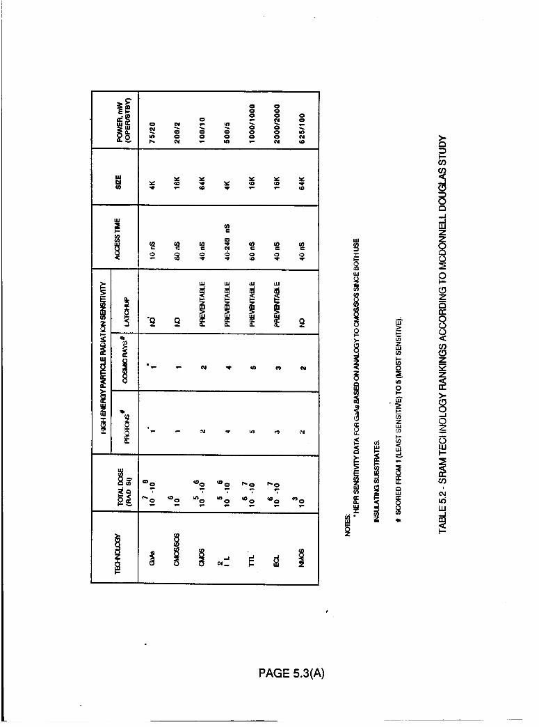
J LPJ Ltl UJ UJ
i i 8 ,
PAGE 5.3(A)
NAS3-24886 FINAL REPORT
that of CMOS/SOS. Gigabit logic currently offers a 1 K, 1 ns GaAs SRAM.
Accurate radiation tolerance performance figures will not be available on
the device until next year. Several 4K devices have been reported with
access times in the 4 ns range in addition to a 16K, 4 ns SRAM [7]. GaAs
SRAMs at the 4K level should be available by the end of 1988. However
they would have to reach at least the 64K level before becoming feasible
for the architectures described in this report. In addition, power
dissipation for the current D-MESFET GaAs RAMs is prohibitively high.HEMT or some other advanced GaAs transistor structure would have to be
commercially available to achieve the higher densities, a prospect at least
several years away. The technology may be worth waiting for as the much
greater speeds would make any of the switching architectures quite
feasible for even higher bit rates.
CMOS or CMOS/SOS RAM technology must still be assumed for the early
1990's. 256K CMOS memories were listed in the parts list in Table 5.1.GaAs RAMs could be assumed if the time frame were to be moved out to
the late 1990's. The discussion in the next section comparing various logic
chip technologies also applies to static RAMs.
5.2 TECHNOLOGY FORECAST FOR CUSTOM AND SEMI-CUSTOM LOGIC
ARRAYS
A list of the custom chips required for the alternative unified memoryarchitecture in the early 1990's is shown in Table 5.3. The chips are
sorted into 3 distinct groups according to their maximum clock rates and
approximate gate complexities (expressed in terms of the number of
gates) are given. The gate complexities for the 1.2 GHz chips should be
quite accurate as the chips have a very regular structure. The other chip
densities are more difficult to estimate and only absolute maximum
numbers are given. Because the three groups represent such a wide range
of clock rates, the future prospects of each group are discussed
separately.
PAGE 5.4
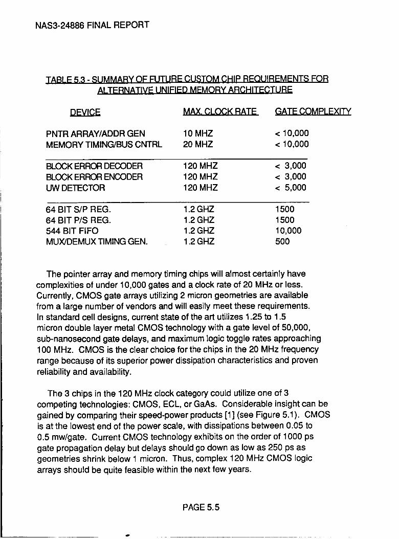
NAS3-24886 FINAL REPORT
TABLE 5.3 - SUMMARY OF FUTURE CUSTOM CHIP REQUIREMENTS FOR
ALTERNATIVE UNIFIED MEMORY ARCHITECTURE
DEVICE MAX. CLOCK RATE GATE COMPLEXITY
PNTR ARRAY/ADDR GEN
MEMORY TIMING/BUS CNTRL
10 MHZ < 10,000
20 MHZ < 10,000
BLOCK ERROR DECODER
BLOCK ERROR ENCODER
UW DETECTOR
120 MHZ < 3,000
120 MHZ < 3,000
120 MHZ < 5,000
64 BIT S/P REG.
64 BIT P/S REG.
544 BIT FIFO
MUX/DEMUX TIMING GEN.
1.2 GHZ 15O0
1.2 GHZ 1500
1.2 GHZ 10,000
1.2 GHZ 5O0
The pointer array and memory timing chips will almost certainly have
complexities of under 10,000 gates and a clock rate of 20 MHz or less.
Currently, CMOS gate arrays utilizing 2 micron geometries are available
from a large number of vendors and will easily meet these requirements.
In standard cell designs, current state of the art utilizes 1.25 to 1.5
micron double layer metal CMOS technology with a gate level of 50,000,
sub-nanosecond gate delays, and maximum logic toggle rates approaching
100 MHz. CMOS is the clear choice for the chips in the 20 MHz frequency
range because of its superior power dissipation characteristics and proven
reliability and availability.
The 3 chips in the 120 MHz clock category could utilize one of 3
competing technologies: CMOS, ECL, or GaAs. Considerable insight can be
gained by comparing their speed-power products [1] (see Figure 5.1). CMOS
is at the lowest end of the power scale, with dissipations between 0.05 to
0.5 mw/gate. Current CMOS technology exhibits on the order of 1000 ps
gate propagation delay but delays should go down as low as 250 ps as
geometries shrink below 1 micron. Thus, complex 120 MHz CMOS logic
arrays should be quite feasible within the next few years.
PAGE 5.5
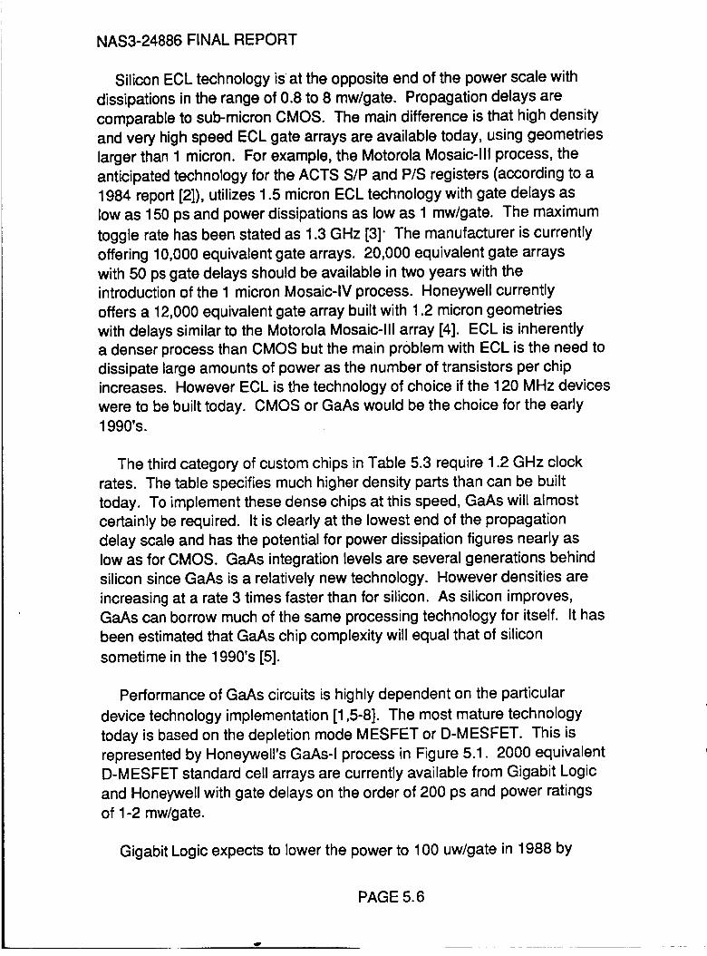
NAS3-24886 FINAL REPORT
Silicon ECL technology isat the opposite end of the power scale with
dissipations in the range of 0.8 to 8 mw/gate. Propagation delays are
comparable to sub-micron CMOS. The main difference is that high density
and very high speed ECL gate arrays are available today, using geometries
larger than 1 micron. For example, the Motorola Mosaic-Ill process, the
anticipated technology for the ACTS SIP and P/S registers (according to a
1984 report [2]), utilizes 1.5 micron ECL technology with gate delays as
low as 150 ps and power dissipations as low as 1 mw/gate. The maximum
toggle rate has been stated as 1.3 GHz [3]" The manufacturer is currently
offering 10,000 equivalent gate arrays. 20,000 equivalent gate arrays
with 50 ps gate delays should be available in two years with the
introduction of the 1 micron Mosaic-IV process. Honeywell currently
offers a 12,000 equivalent gate array built with 1.2 micron geometries
with delays similar to the Motorola Mosaic-Ill array [4]. ECL is inherently
a denser process than CMOS but the main problem with ECL is the need to
dissipate large amounts of power as the number of transistors per chip
increases. However ECL is the technology of choice if the 120 MHz devices
were to be built today. CMOS or GaAs would be the choice for the early
1990's.
The third category of custom chips in Table 5.3 require 1.2 GHz clock
rates. The table specifies much higher density parts than can be built
today. To implement these dense chips at this speed, GaAs will almost
certainly be required. It is clearly at the lowest end of the propagation
delay scale and has the potential for power dissipation figures nearly as
low as for CMOS. GaAs integration levels are several generations behind
silicon since GaAs is a relatively new technology. However densities are
increasing at a rate 3 times faster than for silicon. As silicon improves,
GaAs can borrow much of the same processing technology for itself. It has
been estimated that GaAs chip complexity will equal that of silicon
sometime in the 1990's [5].
Performance of GaAs circuits is highly dependent on the particular
device technology implementation [1,5-8]. The most mature technology
today is based on the depletion mode MESFET or D-MESFET. This is
represented by Honeywell's GaAs-I process in Figure 5.1. 2000 equivalent
D-MESFET standard cell arrays are currently available from Gigabit Logic
and Honeywell with gate delays on the order of 200 ps and power ratings
of 1-2 mw/gate.
Gigabit Logic expects to lower the power to 100 uw/gate in 1988 by
PAGE 5.6
NAS3-24886 FINAL REPORT
introducing the enhancement mode or E-MESFET standard cell array. The
Honeywell E-MESFET performance is shown as_GaAs-II in Figure 5.1
E-MESFET technology is not necessarily faster but it uses much less
power. Gigabit Logic predicts a density level of 10,000 gates by 1988
(See Figure 5.2). Fujitsu has reported on a 16-bit multiplier utilizing a
combination of E and D type MESFETs to achieve a density of 3000 gates
[7].
A third promising GaAs device technology is the high electron mobility
transistor or HEMT. (See the GaAs-III curve in Figure 5.1). Although it
requires more difficult processing technology, it promises even higher
speeds with reduced power consumption. Other technologies are presently
in the early research stages but promise even greater potential. Figure
5.3 shows Gigabit Logic's plans for introducing the various GaAs device
technologies.
Based on the preceding information, it appears that the E-MESFET or
combined E and D MESFET technologies of the early 1990's should be
adequate for the 1.2 GHz custom chips required by the alternative unified
memory architecture. The GaAs chips in Table 5.3 give integration levels
and wattages assuming this technology.
The main technical barrier to the 1.2 GHz circuits in the architecture is
the development of suitable packaging and interconnect tech .nology.
Distances of several inches can represent a significant fraction of a bit
period at those clock rates.
Figures 5.2 and 5.3 courtesy of Gigabit Logic Inc., Newbury Park CA
PAGE 5.7
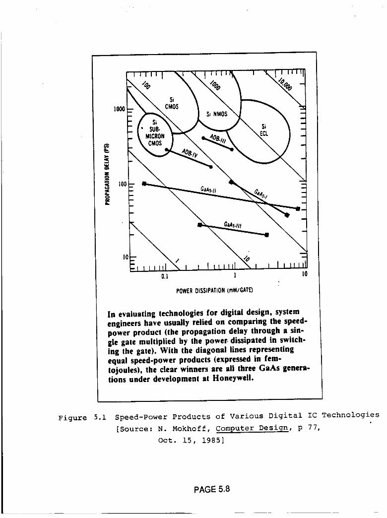
lO00
• SUB-MICRONCMOS
Si NMOS
4S.lll
10/
0.I I I0
POWERDISSIPATION(roW/GATE)
In evaluating technologies for digital design, system
engineers have usually relied on comparing the speed-
power product (the propagation delay through a sin-
gle gate multiplied by the power, dissipated in switch-
ing the gate). With the diagonal lines representing
equal speed-power products (expressed in fem-
tojoules), the clear winners are all three GaAs genera-
tions under development at Honeywell.
Figure 5.1 Speed-Power Products of Various Digital IC Technologies
[Source: N. Mokhoff, Com_uter Desi@n, p 77, '
Oct. 15, 1985]
PAGE 5.8
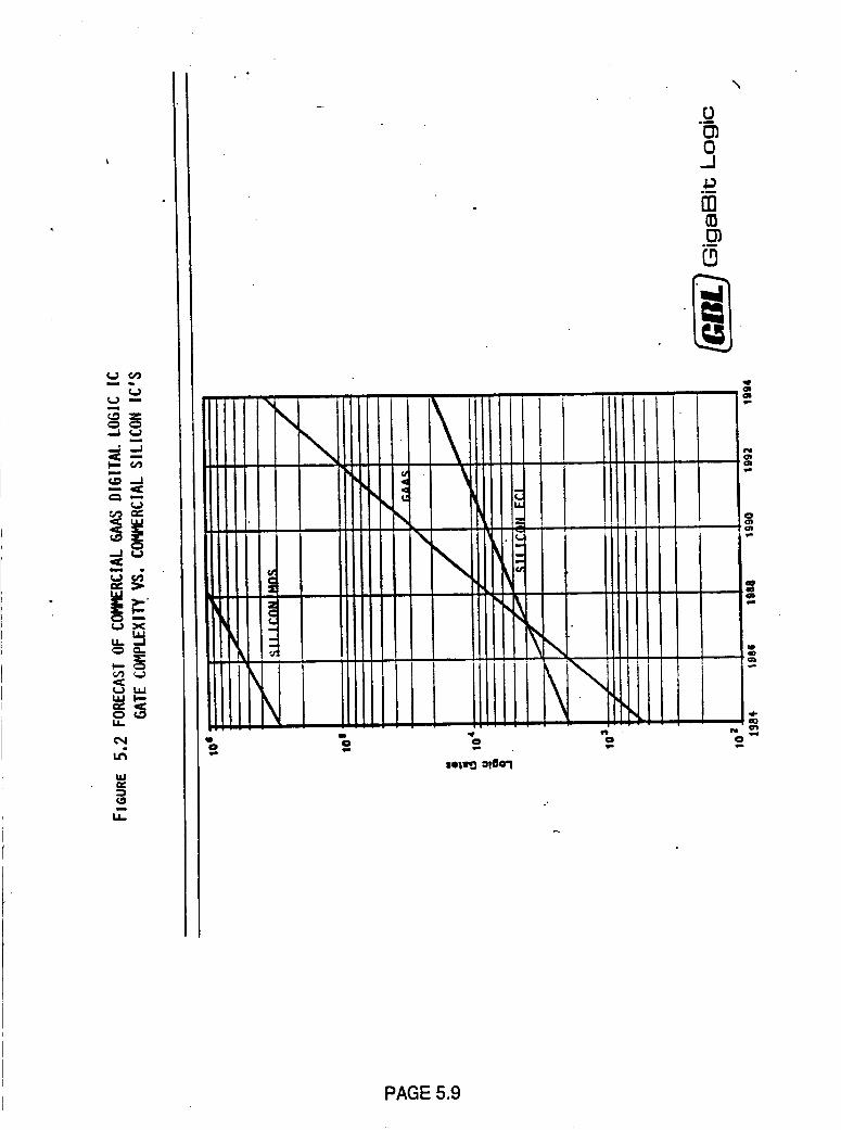
m
m
!.1.1
,...==f,,...) I.iJ
LL
t,IJIZ
tL°°
.gt_0_I
COt_
\
PAGE 5.9
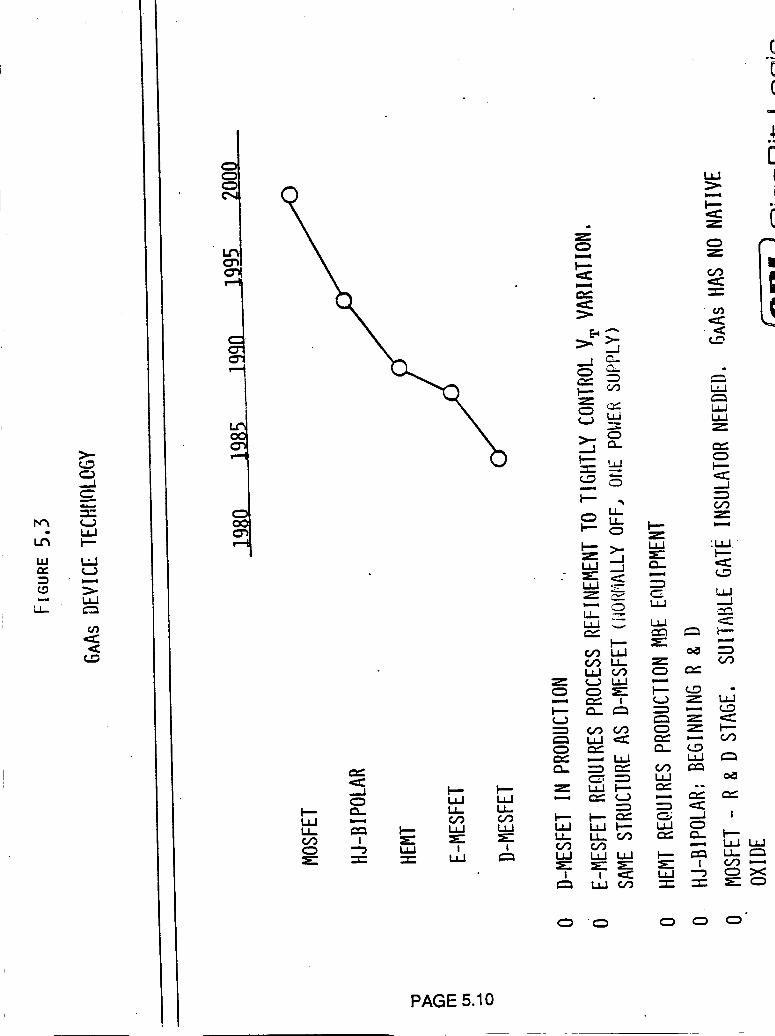
LU
:Z}¢..,9
L.L.
>,,-
.--.I
I.=.JI--"
tJ3
O'J
C
t,m=.
I,.z"OC
I,.=.J
I--ILlLI--¢./3
I-- _ Z
_ _ _ ,,,
_,_ -_ _ X
PAGE 5.10
NAS3- 24886 FINAL REPORT
6.0 TECHNOLOGY DEVELOPMENT REQUIREMENTS
Future technology developments needed to realize a working
destination directed on board packet system comprise:
1) Key Device Development,
2) Destination Directed Packet Architecture Development and
3) Test Bed Development.
Key device development is expected to be aided significantly by
continuing pressures in the semiconductor industry to pursue the most
competitive technologies needed for both military and commercial
applications. Guided development in areas of particular importance to
NASA applications can accelerate the process. Regarding the destination
packet architecture development, this is uniquely related to the onboard
processing structure defined in this document and must be done by NASA if
the approach is to be realized in the future. The concepts involved are
unique and are not being pursued widely by others. The Test Bed is
recommended principally as a vehicle to implement the detailed protocols
that would come from a destination packet architecture development. It
would not only provide a means to demonstrate the technique but more
importantly provide an opportunity to learn by the requirement to apply
the technology and provide a means to perfect the processing algorithms.These three activities are summarized below.
6.1 KEY DEVICE DEVELOPMENT
The feasibility of a high-capacity destination directed packet
switching architecture by the early 1990's assumes the availability of
several key devices. Speed, gate densities, and power dissipation
characteristics must be significantly improved over today's technology for
many of these devices. Refer to Table 5.1 for a parts list of the
alternative unified memory architecture. Logic devices and memory
devices are treated separately below.p
PAGE 6.1
NAS3- 24886 FINAL REPORT
6.1.1 CUSTOM LOGIC DEVICES
A list of the custom logic devices required is given in Table 5.3. The
devices can be broken down into three categories:
1. Standard CMOS logic arrays - <10,000 gate density, <20 MHz clock
Available using today's technology.
. ECL, CMOS, or GaAs logic arrays - <5000 gate density, 120 MHz
clock. Probably within today's ECL technology. Future GaAs or
CMOS technology desirable for reduced power (100 uWatt per gate).
3. GaAs logic arrays 500-10,000 gate densities, 1200 MHz clock.
Requires future advanced GaAs technology. 100 uWatt per gate.
The most critical item listed in Table 5.3 is the 544 bit FIFO with a
clock rate of 1200 MHz. It should be contained in a single chip with a
maximum power dissipation under two watts. The technology listed in
item 3 above must be available for this to be possible.
6.1.2 MEMORY DEVELOPMENT
Section 5.1 discusses future semiconductor RAM technology. Static
RAMs with densities of at least 256K are required to keep system chip
count at an acceptable level. RAM access times depend on the final
architecture implementation, but probably should be about 100 ns. As
discussed in Section 5.1, the limiting factor will be memory device
reliability and radiation tolerance at the densities required. Current
radiation hardened CMOS RAMs are about two generations behind the 256Klevel. GaAs devices are desirable but will not reach the 256K level for at
least the next 5-10 years.
6.2 DESTINATION DIRECTED PACKET ON BOARD PROCESSING ARCHITECTURE
DEVELOPMENT
Section 3.1 provides the system design for a destination directed
packet on board processing architecture. Preliminary tradeoff analyses
are provided which are used to develop key system parameters, such as
packet length, frame size and efficiency. Additional detailed analysis is
needed to firm up the syste m design in order to provide a fully optimized
PAGE 6.2
NAS3- 24886 FINAL REPORT
system.
Issues which require further definition include: DAMA protocols including
method of capacity allocation, burst time plan protocols, packet error
control, packet flow control, acquisition and synchronization procedures,
on board processor port mapping and control procedures.
6.3 DESTINATION DIRECTED PACKET NETWORK CONTROL TEST BED
The proposed architecture utilizes many new system concepts and
requires a hardware implementatiOn substantially different from existing
satellite architectures. A proof-of-concept (POC) test bed is
recommended to demonstrate the architecture feasibility, reveal potential
problems, and assess performance.
6.3.1 CRITICAL FEATURES TO BE INVESTIGATED
The test bed will be used to examine the performance of the
destination directed packet system implemented with the proposed
unified memory architecture. The learning experience will permit further
refinement of the system design. In addition, it is proposed to assess the
system performance under various traffic conditions, determine memory
control complexity, perform a reliability analysis, determine redundancy
requirements, and explore methods of fault detection and onboard
diagnostics.
6.3.2 PROPOSED POC TEST BED BREADBOARD
A POC Test Bed model should be scaled down sufficiently to facilitate
construction with today's technology while still employing all the major
architectural subsystems and features. Figure 6.1 shows a proposed block
diagram. It would interconnect three 40 Mbit/s uplinks and downlinks
operating in three hopping beams. Input and and output multiplexers
operate at rates of 120 Mbit/s in conjunction with a unified data RAM
memory using the "in place" switching architecture. A memory control
CPU accepts the addressing information, modifies the packet headers and
controls the unified memory to accomplish the appropriate channel routing
from upbeam to downbeam time locations.
PAGE 6.3
NAS3- 24886 FINAL REPORT
A POC development program consisting of several phases over an 18
month period shown in Figure is suggested as the next appropriate step in
the evolution of the destination directed onboard switching processor. The
program would consist of the following phases:
1) ARCHITECTURE AND PROTOCOL DEVELOPMENT,
2) HARDWARE DESIGN,
3) TEST BED IMPLEMENTATION,
4) TEST AND EVALUATION
Phase 1 of the test bed program develops the architecture and
protocols for defining the destination directed packet system. System
requirements will be further refined to size the test bed in terms of its
speed and memory size. Architecture tradeoffs will be performed to
develop a system implementation that provides optimum performance with
minimum onboard processor power and mass. Development of terrestrial
interface protocols is needed to accommodate signalling and supervisory
functions of the terrestrial network. The onboard processor routing
protocols will be defined in detail permitting full definition of the control
logic. The destination directed message structure presented in the current
study will be evaluated in detail for the impact of error in transmission to
develop a robust control logic.
Phase 2 develops the hardware using the results obtained from the
architecture and protocol development work described above. This work
will arrive at the design specifications and the design details for the test
bed and its test and evaluation interface facility. During this phase of the
program, memory and logic devices will be selected for constructing the
test bed. The test bed design and its implementation will encompass all
of the functions needed to demonstrate the message directed concepts
developed during the first phase of this program. The througput of the
processor will be scaled down to 120 mbit/s ( comprising three 40 mbit/s
up link beams) to permit implementation with existing device technology.
The test and evaluation interface facility is the means by which the
operator accesses and controls the test bed and collects the test data.
Phase 3 of the test bed program implements and tests individual test
PAGE 6.4
NAS3- 24886 FINAL REPORT
bed modules. Next these are assembled into the complete test bed system.
Early in this phase, a selection will be made of the method of packaging
and the type of circuit board technology to be used. Issues such as
component and system packaging, heat dissipation, intercomponent delay,
race effects and mechanical design and will be addressed.
Phase 4 of the test bed program comprises the test and evaluation
phase. A detailed test plan will be written to describe the test bed
verification and 'end-to-end' system tests. The verification test will
confirm that the test bed meets the design specifications. The
'end-to-end' system tests will assess the overall performance of the
destination directed packet approach. These tests will include an
assessment of throughput efficiency, immunity to blocking, immunity to
channel error, adaptability to track changes in traffic patterns on a
channel by channel basis and exercising burst time plan changes. In
addition, the test bed will be used to refine the onboard routing protocols
by testing performance with a variety of alternatives. The principal
objective of the test bed is to explore the sensitivity of the destination
directed switch concept to its environment and to optimize its operating
protocols.
PAGE 6.5
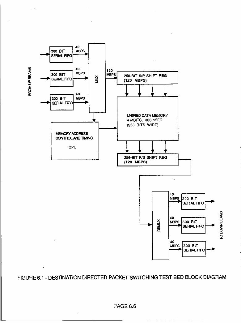
J300 BIT
_ 40 12_
300 BIT I MBPS_ ==SERIAL FIFOi =_
I:E0n-U. 4O
SERIAL RFO i v
IIr
MEMORY ADDRESSCONTROL AND TIMING
CPU
v
256-BIT S/P SHIFT REG
(120 MBPS)
UNIRED DATA MEMORY4 MBITS, 300 nSEC
(256 BITS WIDE)
II
I i
I 256-BIT P/S SHIFT REG(120 MBPS)
_300 BIT L_
SERIAL FIFO _"-
I_ ==
£
,_300 BIT I ,.._
SERIAL FIFO_"
o
FIGURE 6.1 - DESTINATION DIRECTED PACKET SWITCHING TEST BED BLOCK DIAGRAM
PAGE 6.6
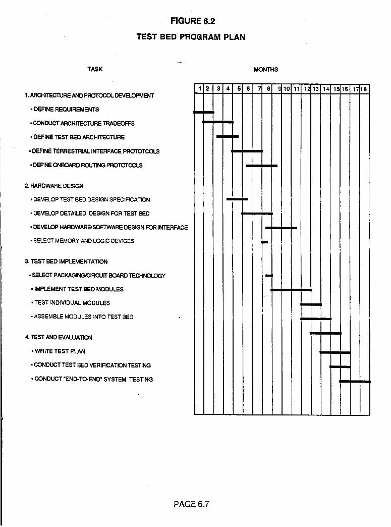
RGURE 6.2
TEST BED PROGRAM PLAN
TASK
1. ARCHITECTURE AND PROT(_,OL DEVELOPMENT
• DEFINE REQUIREMENTS
• CONDUCT ARCHITECTURE TRADES
• DEFINE TEST BED ARCHITECTURE
• DERNE TERRESTRIAL INTERFACE PROTOTCOLS
• DEFINE (_IBOARD ROUTING PROTOTCQ.S
2. HARDWARE DESIGN
• DEVELOP TEST BED DESIGN SPECIFICATION
• DEVELOP DETAILED DESIGN FOR TEST BED
• DEVELOP HARDWARE/SOFTWARE DESIGN FOR INTERFACE
• SEI. !::CT M_MORY AND LOGIC DEVICES
3. TEST BED IMPLEMENTATION
• SELECT PACKAGING/CIRCUIT BOARD TECHNOLOGY
• IMPLEMENT TEST BED MODULES
• TEST INDIVIDUAL MODULES
• ASSEMBLE MODULES INTO TEST BED
4. TEST AND EVALUATION
• WRITE TEST PLAN
• CONDUCT TEST BED VERIFICATION TESTING
• CONDUCT "END-TO-END" SYSTEM TESTING
12345
mm
mmR
Rm
MONTHS
6 7 8 c_10;1112131415161718
me
m
m_BII
mm
PAGE 6.7
NAS3-24886 FINAL REPORT
7.0 REFERENCES
1. N. Mokhoff, "Gallium arsenide Challenges silicon in high-speed
systems," Computer Design, Vol 24, pp 70-78.
2. Motorola Inc., "30/20 GHz communications system baseband
processor subsystem phase 1 final report," (submitted in fulfillment
of contract NAS3-22502), pp 4-64 to 4-68, March 1, 1984.
3. B. Cole, "Motorola grabs lead in ECL density using Mosaic II1,"
Electronics, vol. 60, pp 71-73, Feb. 19, 1987.
4. W. Andrews, "ASICs outlook: dust off predictions from 1986 and
use them again in 1987," EE Times, pp T40, T42+, Dec 8, 1986.
5. G. Johnsen, "Gallium arsenide chips emerge from the lab," High
Technoiogy, Vol 4, pp 44-51, July 1984.
6. D. Bursky, "Digital GaAs ICs emerge from the lab with improved
materials, structures," Electronic Design, vol. 33, pp 79-88, Dec 12,1985.
7. T. Sugeta et al., "High speed technology comparison - GaAs vs Si -,"
GaAs IC Symp. Tech. Dig., pp 3-6, 1986.
8. L. Larson et al., "GaAs high-speed digital IC technology: an
overview," Computer, Vol 19, pp 21-27, Oct 1986.
9. S. Asai, "Semiconductor memory trends," Proc. IEEE, vol 74, pp
1623-1633, Dec 1986.
10. W. Hanna and P. Panagos, "Radiation immune RAM semiconductor
technology for the 80's," Proc. IEEE National Aerospace and
Electronics Conference (NAECON 83), vol 1, pp 604-610, 1983.
11. T.Y. Yan and V.O.K. Li, "A Reliable Pipeline Protocol for the
Message Service of Land Mobile Satellite Experiment" JPL Report.
PAGE 7.1
" NAS3-24886 FINAL REPORT
12. Victor O. Li, "An Integrated Voice and Data Multiple-Access
Scheme for a Land Mobile Satellite System", Proceedings of the IEEE,
Vo1.72, No.11, November 1984.
13. T.Y.Yan and F.M. Naderi, "A Proposed Architecture for aSatellite-based Mobile Communications Network: The Lowest Three
Layers"
14. Charles C. Wang and Tsun- Yee Yan, "Combined Coding and
Delay-Throughput Analysis for Fading Channels of Mobile Satellite
Satellite Communications",lEEE International Conference on
Communications, June 1986, Toronto, Canada.
PAGE 7.2
NAS3-24886 FINAL REPORT
APPENDIX 1
ONBOARD BASEBAND SWITCH CALL PROCESSING
The principal function of the onboard baseband switch is to route
calls assigned to time slots on various carriers in various beam uplinks to
other time slots assigned to carriers in various beam downlinks. TDMA
digital transmission is used because it: a) provides the ease and flexibility
to assign and reassign traffic simply by manipulating the duration and
location of digital data bursts and b) it is the only way to provide the
flexibility to accommodate beam hopping. This discussion is devoted to the
functioning of the call processing in a baseband switch designed for
serving such a TDMA implemented muitibeam hopping system. A question
to be addressed is the merit of including the capability to perform call
processing as part of the onboard processing rather than performing it at a
ground Network Control Center. The principal merit would lie in the
reduction of the transmission load on the control link between the
satellite and the earth. The conclusion is that there is not significant
merit for performing call processing onboard with the circuit switched
mode of operation. However, there may be significant merit for onboard
destination directed switching for both voice and data.
ONBOARD CIRCUIT SWITCHING
Figure I illustrates the principal components of a baseband switch
used to route a call from an upbeam burst to a downbeam burst in a beam
hopping system. For the sake of simplicity, an implementation for onty two
beams is shown, the extension to a greater number of beams being
apparent. This configuration corresponds to that being used on the ACTS.
At the left side of the diagram are two Input Data Memories which are
used to store the traffic bursts arriving from each of two hopping uplink
beams. Each of Data Memory actually contains two memories operating in a
ping-pong fashion where one memory is being filled with new data in the
current TDMA frame while the contents of the other, which were collected
in the previous frame, are being processed by the switch. The storing and
playback functions alternate for each memory from TDMA frame to TDMA
frame. In the ACTS the TDMA frame period is 1 ms and each telephone
channel carries 64 kbit/s PCM, hence each channel comprises 64information bits.
PAGE A1.1
NAS3-24886 FINAL REPORT
At a transmission rate of 110,592 kbit/s,the uncoded transmission
rate used on the ACTS, each frame can accommodate 1728 telephone
channels. It is assumed for the purpose of this discussion that each input
memory serves the capacity of one such TDMA carrier and there is one
carrier per beam. Hence, there are 1728 64 bit telephone channel slots in
each of the input memories. The function of the baseband switch is to
route individual channel slot contents to their proper destination slot in
one of the down link beams. Figure 1 illustrates the routing for uplink slot
V in beam 1 to downlink slot Y in beam 1 and uplink slot W in beam 2 to
downlink Slot Z in beam 2. The switch is implemented as a
time-space-time (TST) switch. Traffic arriving on each of the uplink
beams is stored in the input memories in the time order of arrival as
established by the burst time plan structure of TDMA stations.
Playback of the contents of the input data memories is controlled by
the input control memories which operate in a sequential fashion to
address the contents of the input data memories and cause them to be
presented to the route switch. The route switch constitutes the space
switch of the TST configuration. The function of the route switch is to
direct the selected contents of the input memories to the appropriate
output memories. The Route Switch Memory identifies which of the states
of the route switch applies to the currently selected channels. For the 2x2
route switch assumed in this example, the total number of p6_ssible states
are 16 as illustrated in Figure 2. In general, the total number of states of
a MxN route switch is theoretically 2 MN and hence can become very large
even for a small number of multiple beams. Care must be exercised to use
only the states that are needed and to code these in an efficient way. The
route switch presents the selected input data memory channel slot
contents to the locations in the output memory designated by the contents
of the output control memories. The entire process of transfer of the
contents of all of the input data memories to the output data memories
occurs in one TDMA frame period. The output memories operate in a
ping-pong fashion like the input memories. Each ping-pong memory is
filled on one TDMA frame period and played out on the next. The delay in
passage through the entire switch is 2 ms. The order of storage in the
output memories is controlled by the sequence of the route switch memory
while the order of playback is controlled by the output control memories.
PAGE A1.2e
NAS3-24886 FINAL REPORT
For each time slot occurring on the uplink beams, there will exist a
current routing switch state selected to carry the traffic from a
particular uplink beam to a particular downlink beam. For a 2x2 beam
system the routing possibilities are:
INPUT 1 TO OUTPUT 1
INPUT 1 TO OUTPUT 2
INPUT 2 TO OUTPUT 2
INPUT 2 TO OUTPUT 1
2,6,9,10,14,15,16
4,6,7,11,12,13,15,16
3,7,8,10,12,13,14,16
5,8,9,11,13,15,16
The numbers given after each route possibility identify the 2x2 switch
states that will provide the connection indicated. Switch state 1 is a
no-connect state an is the initial state from which to begin. Some of the
states may not be used. If only those corresponding to non broadcast or non
convergence operation are included, only switch states 1,2,3,4,5,10 and
11, a total of seven, would be used. Similar arrangements will exist for
other larger multiple beam systems. When a call is to be setup, an
uptink slot must be picked for which the existing switch state is one that
allows the wanted beam-to-beam connection to be made. To accomplish
this, it is necessary that a record be kept of the route switch state
currently in use for each uplink channel slot. This record may be kept in
terms of lists, one for each type of routing, which identify the addresses
of the addresses of channel slots currently using a switch state that can
accommodate the routing type. For the 2x2 switch there are four such
lists, viz., 1 to 1,2 to 2, 1 to 2, and 2, to 1. In general there are N2 of
these lists for an NxN beam system.
CONNECTING A CALL THROUGH THE SWITCH
A procedure for connecting a call through the onboard basebandswitch is now identified:
1) Identify the beam to beam routing needed to carry the call.
2) From the route-type lists, identify an uplink slot address and
switch state type that can accommodate the connection.
3) Pick an available route switch address, say X.
PAGE A1.3
NAS3-24886 FINAL REPORT
4)
S)
6)
7)
Modify the route switch type to accommodate the new connection
and update the route-type lists.
Determine an input control memory address. If the route switch
address is X, then set the input control memory address to X-I.
Determine an output control memory address. If the route switch
address is X, then set the output control memory address to X+I.
Determine from the Uplink Data Memory Map an available input
data control memory address and corresponding uplink channel slotnumber.
8) Determine from the Downlink Traffic Map an available
downlink channel slot address, say Y for beam 1 or Z for beam 2
and set the downlink control memory address to Y-1 or Z-1 as
appropriate.
The above steps are performed each time a call is connected and a similar
procedure must be used for a call disconnect.
The following messages must be sent to the onboard switch to
implement the connection:
1)Contents of Input Control Memory 1 location X-1 comprising the
address of the Uplink Data Memory 1 to hold the channel data for
uplink time slot V.
2) Contents of Input Control Memory 2 location X-1 comprising the
address of the Uplink Data Memory 2 to hold the channel data for
uplink time slot W.1
3) Contents of Route Switch Memory location X comprising a code
identifying the Route Switch State S.
PAGE A1.4
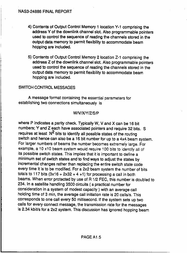
NAS3-24886 FINAL REPORT
4) Contents of Output Control Memory 1 location Y-1 comprising the
address Y of the downlink channel slot. Also programmable pointers
used to control the sequence of reading the channels stored in the
output data memory to permit flexibility to accommodate beam
hopping are included.
5) Contents of Output Control Memory 2 location Z-1 comprising the
address Z of the downlink channel slot. Also programmable pointers
used to control the sequence of reading the channels stored in the
output data memory to permit flexibility to accommodate beam
hopping are included.
SWITCH CONTROL M ESSAGES
A message format containing the essential parameters for
establishing two connections simultaneously is
WNIXlY/Z/SIP
where P indicates a parity check. Typically W, V and X can be 16 bit
numbers; Y and Z each have associated pointers and require 32 bits. S
requires at least N2 bits to identify all possible states of the routing
switch and hence can also be a 16 bit number for up to a 4x4. beam system.
For larger numbers of beams the number becomes extremely large. For
example, a 10 xl0 beam system would require 100 bits to identify all of
its possible switch states. This implies that it is important to define a
minimum set of switch states and to find ways to adjust the states by
incremental changes rather than replacing the entire switch state code
every time it is to be modified. For a 2x2 beam system the number of bits
totals to 117 bits (3xl 6 + 2x32 + 4 +1) for processing a call in both
beams. When error protected by use of R 1/2 FEC, this number is doubled to
234. In a satellite handling 3500 circuits ( a practical number for
consideration in a system of modest capacity ) with an average call
holding time of 3 min, the average call initiation rate is 20 calls/s. This
corresponds to one call every 50 millisecond. If the system sets up two
calls for every connect message, the transmission rate for the messages
is 2.34 kbit/s for a 2x2 system. This discussion has ignored hopping beam
PAGE A1.5

NAS3-24886 FINAL REPORT
pointing, which requires little additional information rate and will not
change the result significantly.
Increasing the number of beams requires additional information tocontrol the onboard switch. The increase in the number and/or size of
control memories is in direct proportion to the increased capacity:
however the increase in the number of routing switch states is
exponential and the number of bits required to express all possible states
increases as the square of the number of beams. This later fact can cause
a more than linear increase in the capacity needed to administer control of
the onboard switch. However this increase is not very significant for 10
beams or less. For 10 beams the number of bits needed for messages to the
control memories is 560 and for the route switch memory 100, yielding a
total of 661 including parity. This must be doubled for R 1/2 FEC to a total
of 1322 bits per 10 calls or 132 per call. The number of bits per call for
the 2x2 beam configuration was 117.
COMPARISON OF ONBOARD VERSUS GROUND CONTROL
The discussion thus far referred to control of the onboard switch
from the ground and identification of the parameters that need to be sent
to the satellite. These parameters have been identified as W,V,X,Y Z,S and
P in the preceding discussion. Consider now what would happen if the
route switch processing where performed onboard. Obviously, those
parameters identifying the uplink and downlink slots, viz W,V,Y and Z and
the parity P would still have to be sent from the ground since these are
determined on the ground where the overall system network control is
performed. This network control function involves the central collection
and processing of all call requests and the generation of the resulting
traffic burst time plans for all stations in the system and the generation
of the instructions that go to the onboard switch including the
determination and control of the states of the routing switch. The only
function that might be transferred to the satellite, outside of transferring
all the network control functions to the satellite, is selection of the
states of the routing switch. The discussion of the preceding section
shows that the control information S pertaining to the route switch does
not constitute a large fraction of the uplink command link data rate even
for a large number of beams. If the function of selecting the route switch
states was implemented on board the satellite, the associated processing
implementation would also have to be onboard thus increasing the onboard
PAGE A1.6

NAS3-24_86 FINAL REPORT
power and weight. The small savings in the command link capacity wouldlikely not be worth the additional expense of having the the route switch
state selection processing performed onboard. As long as the networkcontrol function remains on the ground, the selection of the route switch
states is best done there. However, if a means is implemented onboard todirectly perform routing from destination directed addressing carriedwith the message, route switch state selection would appropriately be apart of the onboard call processing function.
PAGE A1.7
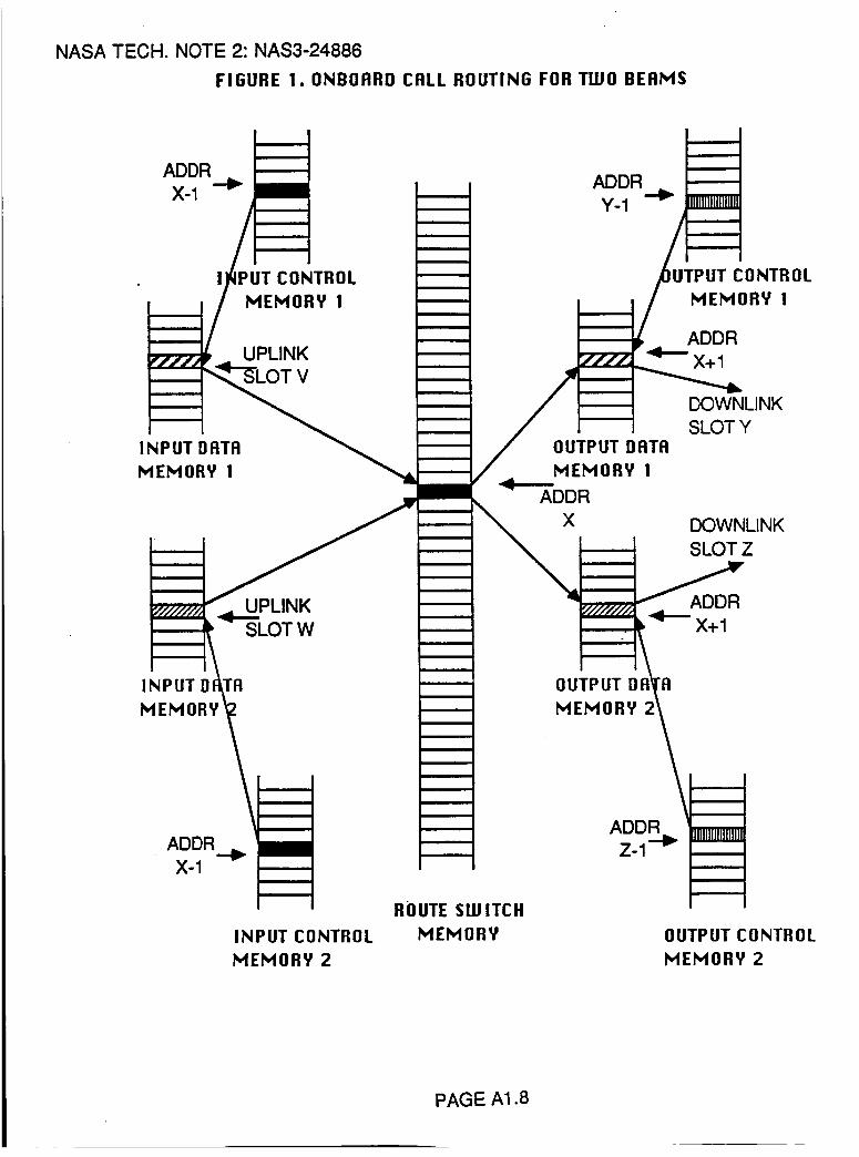
NASA TECH. NOTE 2:NAS3-24886
FIGURE 1. ONBOARD CALL ROUTING FOR TWO BEAMS
PC}DR
X-1I
I
i
I
PUT CONTROL
MEMORY I
UPLINK
V
INPUT DATA
MEMORY I
m
n
_///II///_
i
l
INPUT D
MEMORY
UPLINK
SLOT W
ADDR__.X-1
i
m
ii
INPUT CONTROL
MEMORY 2
I
iI
]
)
lIi
i
ADDR
Y-1
I
I
I
I
i
'I
I
IUTPUT CONTROL
MEMORY I
i ; ADDR
- /! DOWNLINK
_ / SLOT Y
OUTPUT DATA/ MEMORY I
mr 4-- DORX DOWNLINK
SLOT Z
i
i
m
m
m
m
a
ROUTE SW ITCX
MEMORY
OUTPUT [ FA
MEMORY 2
ADDRZ.1--I_
0 UTP UT C
MEMORY
ONTROL
2
PAGE A1.8
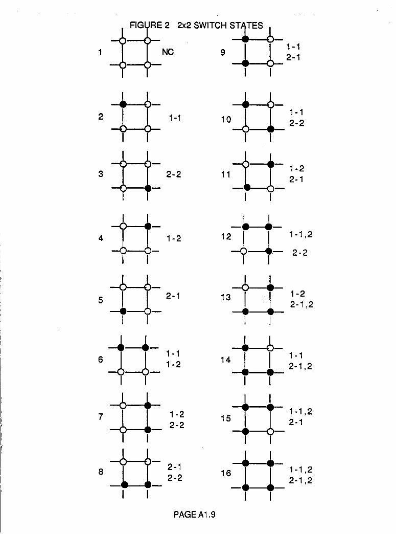
..-.(
.-.-(
2x2 SWITCH
9(I)__ 1-12-1
I I
-,I,--,_- -,!,--_-
I I I I
I I I I
5
I 1 I I
-4,---_-1.11-2
u
I I
7
4---;-1.12-1,2
I I
.-.( ) 2-2 (I I
m
m
___.___ _,___,_,o_;;
I I I I
PAGE A1.9
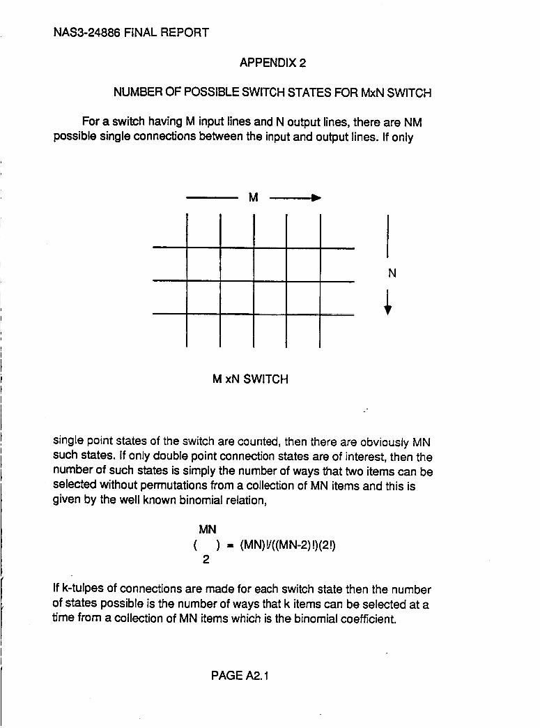
NAS3-24886 FINAL REPORT
APPENDIX 2
NUMBER OF POSSIBLE SWITCH STATES FOR MxN SWITCH
For a switch having M input lines and N output lines, there are NM
possible single connections between the input and output lines. If only
M v
N
M xN SWITCH
single point states of the switch are counted, then there are obviously MN
such states. If only double point connection states are of interest, then the
number of such states is simply the number of ways that two items can be
selected without permutations from a collection of MN items and this is
given by the well known binomial relation,
MN
( ) - (MN)V((MN-2)!)(21)2
If k-tulpes of connections are made for each switch state then the number
of states possible is the number of ways that k items can be selected at a
time from a collection of MN items which is the binomial coefficient.
PAGE A2.1
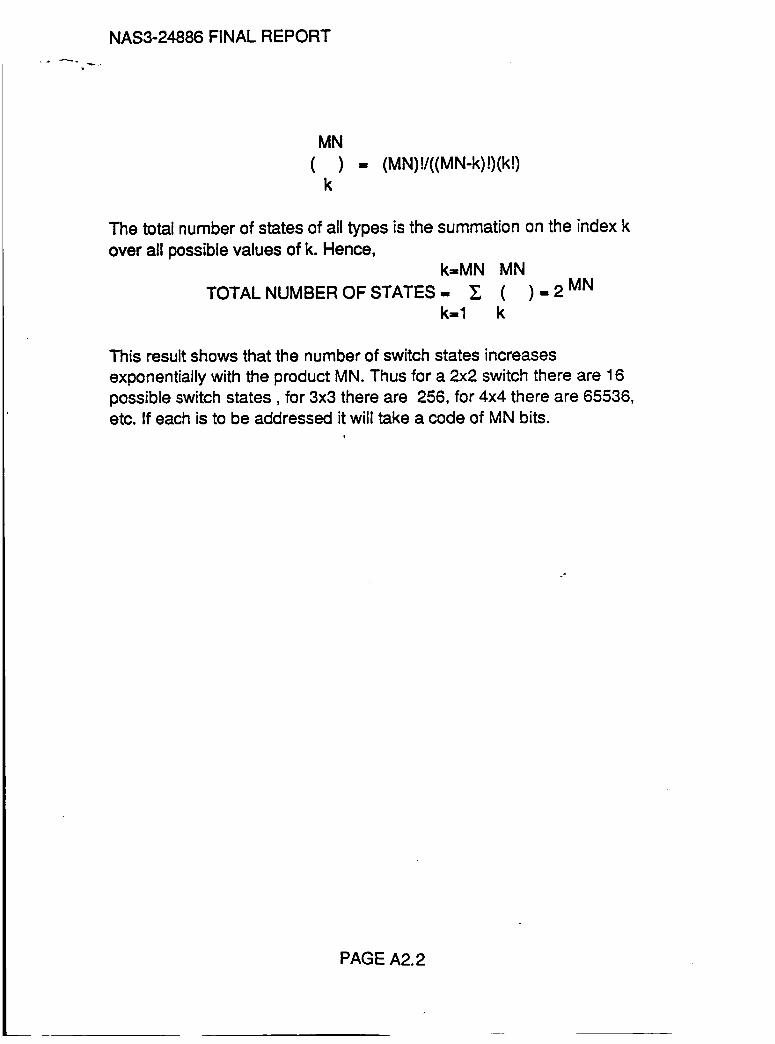
NAS3-24886 FINAL REPORT
MN
( ) = (MN)!/((MN-k)!)(k!)k
The total number of states of all types is the summation on the index k
over all possible values of k. Hence,k=MN MN
TOTAL NUMBER OF STATES- ,T., ( )=2MN
k=l k
This result shows that the number of switch states increases
exponentially with the product MN. Thus for a 2x2 switch there are 16
possible switch states, for 3x3 there are 256, for 4x4 there are 65536,etc. If each is to be addressed it will take a code of MN bits.
PAG E A2.2
National Aeronautics and
Space AOrn,nlsttat,on
I. Report No.
CR1808174. Title and Subtitle
Report Documentation Page
2. Government Accession No. 3. Recipient's Catalog No.
5. Report Date
On-Board Processing Satellite Network Architectureand Control Study
7. Author(s)
S. Joseph CampanellaB. Pontano
H. Chalmers
9. Performing Organization Name and Address
COMSAT22300 Comsat DriveClarksburg, MD 20871
12. Sponsoring Agency Name and Address
NASA-LEWIS Research Center21000 Brookpark RoadC1 .... I:.A 0 _ 44! 35
June 19876. Performing Organization Code
650-20-268. Performing Organization Report No.
10. Work Unit No.
11. Contract or Grant No.
NAS3-24886
13. Type of Report and Period Covered
14. Sponsoring Agency Code
15. Supplementary Notes
16. Abstract
see attached
17. Key Words (Suggested by Author(s)) 18. OistributLon Statement
General Release
19. Security Classif. (of thas report) I 20. Securnty Classd. (of this page) 2t. No of pages
unclassified INASA FORM 1626 OCT 86 "For sale by the Nationat Technical Information Serwce, S_)nngfield, Virg,n,a 22161
22. Price-