observation of coulomb repulsion between cu intercalants
TRANSCRIPT

PHYSICAL REVIEW B 89, 155312 (2014)
Observation of Coulomb repulsion between Cu intercalants in CuxBi2Se3
Chris Mann,1 Damien West,2 Ireneusz Miotkowski,3 Yong P. Chen,3,4 Shengbai Zhang,2 and Chih-Kang Shih1,5,*
1Materials Science & Engineering, University of Texas at Austin, Austin, Texas 78712, USA2Department of Physics, Applied Physics, and Astronomy, Rensselaer Polytechnic Institute, Troy, New York 12180, USA
3Department of Physics, Purdue University, 525 Northwestern Ave., West Lafayette, Indiana 47907, USA4Birck Nanotechnology Center and School of Electrical and Computer Engineering, Purdue University, West Lafayette, Indiana 47907, USA
5Department of Physics, University of Texas at Austin, Austin, Texas 78712, USA(Received 29 October 2013; revised manuscript received 1 April 2014; published 17 April 2014)
Using scanning tunneling microscopy and ab initio simulations, we have identified several configurationsfor Cu dopants in CuxBi2Se3, with Cu intercalants being the most abundant. Through statistical analysis, weshow strong short-range repulsive interactions between Cu intercalants. At intermediate range (>5 nm), the pairdistribution function shows oscillatory structure along the 〈101〉 directions, which appear to be influenced bydifferent diffusion barriers along the 〈101〉 and 〈211〉 directions.
DOI: 10.1103/PhysRevB.89.155312 PACS number(s): 68.37.Ef, 68.35.bg, 71.55.−i
I. INTRODUCTION
Understanding and controlling dopants in semiconductorshas played a critical role in the development of modernsemiconductor technology—the atomic configuration withinthe lattice and the electronic behavior of these (often) in-tentional impurities determines the type and quality of bulkelectronic behavior [1–3]. While the advancement of materialssynthesis techniques, such as molecular beam epitaxy, havebeen aimed at precise control of dopants with atomic-layer pre-cision, including δ-doping schemes [4,5], several atomic-scalemicroscopy investigations have revealed rather complicateddopant distribution functions manifested by effective dopant-dopant interactions [6,7]. In the development of 3D topologicalinsulators (TIs), understanding and controlling dopants isexpected to play a similarly critical role in the materialsadvancement necessary to realize many predicted novel deviceproperties. The behavior of dopants in 3D TIs, such as Bi2Se3,is inherently more complicated due to a significantly largernumber of configurations available to dopants in these layeredhost materials. For instance, while many studies find that Cu isan n-type dopant in Bi2Se3, other studies have found that it canbe used to prevent n-type doping—as an amphoteric defect,intercalated Cu is expected to n-dope the sample and CuBi
substitutions are expected to p-dope the sample [8]. Whileit has been found that heavily doped CuxBi2Se3 becomessuperconducting [9–13], studies thus far have not distinguishedwhere these Cu dopants physically reside in the Bi2Se3 sam-ples. Other studies have found that strong band bending at thesurface has limited Bi2Se3’s viability as a TI, as the bulk con-duction band is pulled down below the Fermi level and allowsnontopological carriers [14–16]; attention has turned towardsresolving these issues through clever doping schemes [17–19].Therefore, understanding how Cu dopants are incorporatedinto the Bi2Se3 lattice is fundamental to understanding theconsequences for the electronic structure and the surface state.
Here, we investigate the role of Cu with an atomic-scale resolution using scanning tunneling microscopy andab initio simulations. We have characterized several Cu defects
*Corresponding author: [email protected]
and, through comparison with simulation, determined theirpositions within the lattice. Statistical analysis of the spatialdistribution of Cu shows that, when intercalated, Cu exhibitsrepulsive potentials characterized by a strong suppression ofthe pair distribution function at short separations. At longerrange (>5 nm), the pair distribution function shows oscillatorystructure along the 〈101〉 directions that is absent along the〈211〉 directions.
II. EXPERIMENTAL DETAILS
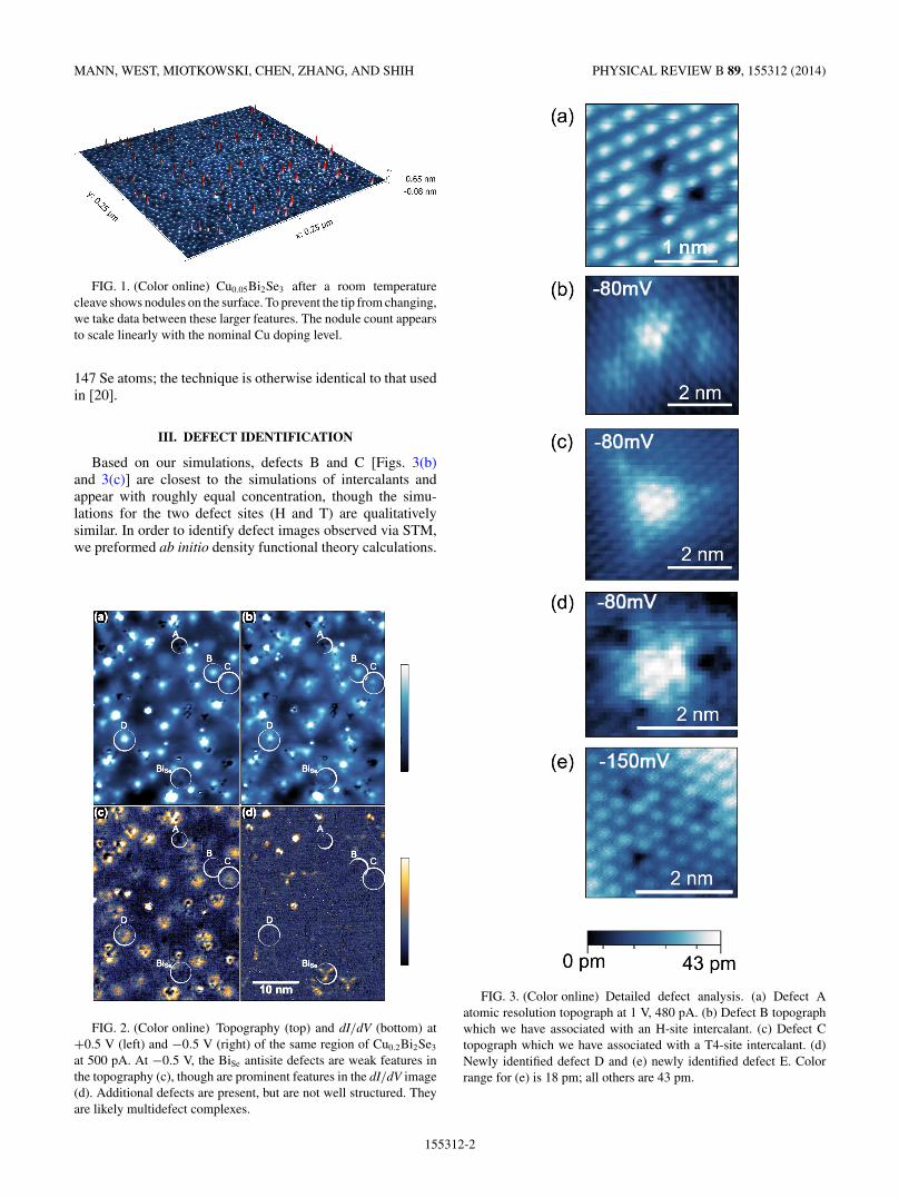
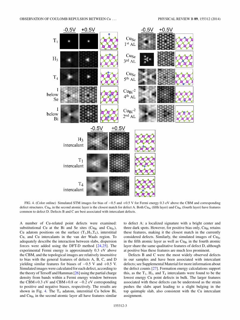
Samples were grown using a Bridgman-type method similarto Mann et al. [20] and were prepared for analysis bycleaving in ultrahigh vacuum (UHV) at room temperature, thenimmediately transferred to the STM at 77 K. By cleaving thesingle-crystal samples, we are able to investigate the structureof the as-cleaved surface and near subsurface, the regime asso-ciated with topologically interesting behavior—we are unableto determine whether this is representative of the bulk structure.We observed �500 pm nodules on the cleaved surface that weattribute to previously intercalated Cu that, upon cleaving,rearranged into clusters, shown in Fig. 1. The concentration ofthese nodules scales roughly linearly with the nominal bulkconcentration of Cu, providing further evidence that thesenodules are Cu clusters. All high resolution data was acquiredin regions away from these large defects. Smaller defects withidentifiable structure are visible in Figs. 2(a) and 2(b)—inaddition to the nodules, we can identify five additional defectsthat are not observed in nominally undoped Bi2Se3, labeleddefects A–E (only defects A–D are visible in Fig. 2).
Though Cu intercalants have long been expected to bethe origin of n-doping in CuxBi2Se3 [8,10], a quantitativepicture of the electronic interaction has not been developed,though their effect on strain has been noted [21]. We observedseveral Cu defects in CuxBi2Se3 with different topographicand tunneling signatures [Figs. 2(a)–2(d)], several of whichhave been observed by STM before (defects A–C) [11,22,23];however, because STM lacks chemical specificity, we cannotdefinitively identify these defects without resorting to ab initiosimulations of STM topographs. To simulate the Cu defects,we performed density functional theory calculations withsingle (7 × 7) quintuple-layer (QL) slabs using 98 Bi and
1098-0121/2014/89(15)/155312(7) 155312-1 ©2014 American Physical Society
MANN, WEST, MIOTKOWSKI, CHEN, ZHANG, AND SHIH PHYSICAL REVIEW B 89, 155312 (2014)
FIG. 1. (Color online) Cu0.05Bi2Se3 after a room temperaturecleave shows nodules on the surface. To prevent the tip from changing,we take data between these larger features. The nodule count appearsto scale linearly with the nominal Cu doping level.
147 Se atoms; the technique is otherwise identical to that usedin [20].
III. DEFECT IDENTIFICATION
Based on our simulations, defects B and C [Figs. 3(b)and 3(c)] are closest to the simulations of intercalants andappear with roughly equal concentration, though the simu-lations for the two defect sites (H and T) are qualitativelysimilar. In order to identify defect images observed via STM,we preformed ab initio density functional theory calculations.
FIG. 2. (Color online) Topography (top) and dI/dV (bottom) at+0.5 V (left) and −0.5 V (right) of the same region of Cu0.2Bi2Se3
at 500 pA. At −0.5 V, the BiSe antisite defects are weak features inthe topography (c), though are prominent features in the dI/dV image(d). Additional defects are present, but are not well structured. Theyare likely multidefect complexes.
FIG. 3. (Color online) Detailed defect analysis. (a) Defect Aatomic resolution topograph at 1 V, 480 pA. (b) Defect B topographwhich we have associated with an H-site intercalant. (c) Defect Ctopograph which we have associated with a T4-site intercalant. (d)Newly identified defect D and (e) newly identified defect E. Colorrange for (e) is 18 pm; all others are 43 pm.
155312-2
OBSERVATION OF COULOMB REPULSION BETWEEN Cu . . . PHYSICAL REVIEW B 89, 155312 (2014)
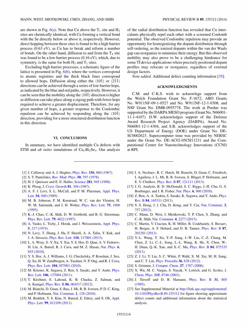
FIG. 4. (Color online) Simulated STM images for bias of −0.5 and +0.5 V for Fermi energy 0.3 eV above the CBM and correspondingdefect structures. CuBi in the second atomic layer is the closest match for defect A. Both CuSe (fifth layer) and CuBi (fourth layer) have featurescommon to defect D. Defects B and C are best associated with intercalant defects.
A number of Cu-related point defects were examined:substitutional Cu at the Bi and Se sites (CuBi and CuSe),Cu adatom positions on the surface (T1,H3,T4), interstitialCu, and Cu intercalants in the van der Waals region. Toadequately describe the interaction between slabs, dispersionforces were added using the DFT-D method [24,25]. Theexperimental Fermi energy is approximately 0.3 eV abovethe CBM, and the topological images are relatively insensitiveto bias with the general features of defects A, B, C, and Dyielding similar features for biases of −0.5 V and +0.5 V.Simulated images were calculated for each defect, according tothe theory of Tersoff and Hamman [26] using the partial chargedensity from bands within a Fermi energy window betweenthe CBM+0.3 eV and CBM+0.8 or −0.2 eV correspondingto positive and negative biases, respectively. The results areshown in Fig. 4. The T4 adatom, interstitial Cu below Bi,and CuBi in the second atomic layer all have features similar
to defect A: a localized signature with a bright center andthree dark spots. However, for positive bias only, CuBi retainsthese features, making it the closest match in the currentlyconsidered defects. Similarly, the simulated images of CuSe
in the fifth atomic layer as well as CuBi in the fourth atomiclayer share the same qualitative features of defect D, althoughat positive bias these features are much less prominent.
Defects B and C were the most widely observed defectsin our samples and have been associated with intercalantdefects; see Supplemental Material for more information aboutthe defect counts [27]. Formation energy calculations supportthis, as the T1, H3, and T4 intercalants were found to be thelowest energy Cu point defects in bulk. The larger featuresassociated with these defects can be understood as the strainpushes the slabs apart leading to a slight bulging in thetop quintuple slab, also consistent with the Cu intercalantassignment.
155312-3

MANN, WEST, MIOTKOWSKI, CHEN, ZHANG, AND SHIH PHYSICAL REVIEW B 89, 155312 (2014)
FIG. 5. (Color online) (a) 200 nm×200 nm topography of nominallyCu0.05Bi2Se3 showing 1020 Cu inter-calants, white spots, and Cu clusters,red dots. (b) Radial distribution func-tion of Cu intercalants extracted from(a) along directions of major symmetry.(c) A repulsive interaction is shownby the potential of mean force, deter-mined by taking the log of the radialdistribution function (solid line). Thedotted line is a fit to the Yukawa po-tential; the screening length was foundto be 3.9 ± 0.4 nm. The normalizationfactor was determined by computingthe radial distribution function for anensemble of random distributions andis plotted with its pointwise standarddeviation in (d). To determine whetherthe structure within the radial dis-tribution functions is within 1σ , wenormalized the distribution functionsalong 〈101〉 and 〈211〉 by R∗(r1,r2) ±σ , as shown in (e) and (f). The latticevectors are plotted on top of a C-type defect (g). The observed structureindicates that the preferred orderingat this intercalant density is similarto that shown in (h). The observeddirectional anisotropy is attributed todiffusion barrier anisotropy: hoppingalong sites in the 〈101〉 direction has alower barrier than the 〈211〉 direction,as shown by the lattice sites in (i).
IV. STATISTICAL ANALYSIS
Qualitatively, we noticed that the Cu intercalants are rarelyfound to be overlapping—they appear to maintain distancefrom each other, implying a repulsive interaction betweenintercalants. Quantitatively, this effect can be expressed by thepair distribution function, P(r1,r2), the result of which is shown
in Fig. 5(b), based on the analysis of 1020 intercalants (B andC type) in a 200 nm × 200 nm window [Fig. 5(a)]. Note thatin this statistical analysis, we make a distinction between thepair distribution functions along two inequivalent directions,〈101〉 and 〈211〉. Also shown in Fig. 5(d) is the random pairdistribution, denoted R∗(r1,r2), which is generated using the
155312-4

OBSERVATION OF COULOMB REPULSION BETWEEN Cu . . . PHYSICAL REVIEW B 89, 155312 (2014)
results of 100 000 random ensembles, each with identicaldefect counts and box dimensions as the STM data, similarto Ref. [7]. The range of ±1σ statistical fluctuations due tothe finite ensemble size is shown as the shaded area. Becausethis data was acquired at 77 K, there is some residual driftthat can produce uncertainty in the position of the defects.Therefore, the calculation uses a kernel density method with aGaussian kernel width of 1 nm. Furthermore, the calculationassumes a continuum (not a lattice model), so any data pointsbelow separation of 0.5 nm are not meaningful. Nevertheless,the strong suppression of the pair distribution in short pairseparation (<5 nm) is quite evident.
To interpret the origin of this suppression of pair distributionat short distance, we plot the pair correlation function,defined as the ratio of the actual distribution to the randomdistribution, C(r1,r2) = P (r1,r2)/R∗(r1,r2), in logarithmicscale as −lnC(r1,r2) versus the pair separation [Fig. 5(c)].The pair correlation function can be associated to the effectivepair interaction potential as w(r1,r2) = −kBT ln[C(r1,r2)].The functional form of the pair correlation function suggeststhat the pair interaction is of screened-Coulombic nature. Thescreened Coulomb potential (or often referred to as the Yukawapotential) has a functional form of ϕ(r) ∼ 1
re−κr , which is
plotted as the dashed curve with κ = 0.25 nm−1, correspondingto a screening length of 3.9 ± 0.3 nm. As these intercalantCu atoms are n-type dopants and should have a charge stateof +1, it is not surprising that there is Coulomb interactionbetween them. Interestingly, this is in contrast to the surface Cuadatoms, which prefer to arrange into clusters. Because thereis a strong near-surface band-bending field, the local Fermilevel is n-shifted, making ionization unfavorable [14]; we havepreviously estimated this field to be �150 meV/nm [20].
Note that the Fermi energy of this sample is roughly 0.3 eVabove the conduction band minimum. With an effective massof 0.15mo [10], one can deduce a Fermi wavelength of λF �5.5 nm. For an electronic system, the screening length shouldbe of the same order of magnitude as the Fermi wavelength.Thus a screening length of �4 nm strongly suggests that thefree carriers provide the screening of Coulomb interactionsbetween intercalants. In addition to a clear signature ofshort-range repulsive interactions, one also observes anoscillatory structure in the pair correlation function alongthe 〈101〉 directions (but not along the 〈211〉 directions). Toverify that this is not noise, we normalized the pair correlationfunctions by R∗(r1,r2) ± σ , as shown in Figs. 5(e) and 5(f).The 〈101〉 directions show additional structure to within ±σ ,while the 〈211〉 directions do not.
V. CONSEQUENCES AND INTERPRETATION OFOSCILLATIONS IN C(r1,r2)
The observed oscillations of C(r1,r2) along the 〈101〉 direc-tions raises some interesting questions and evokes comparisonto dopants in other systems. This oscillatory phenomenon isfundamentally different from Friedel oscillation phenomenareported previously for adsorbates on metal surfaces [28,29].For Friedel oscillations, the period should be half of the Fermiwavelength, while the observed period is a factor of 2 longer,which may suggest the existence of higher order correlations.On the other hand, the interaction of Cu intercalants with
FIG. 6. (Color online) (a) Climbing image nudged elastic bandcalculation [34] of the kinetic barrier for diffusion of intercalated Cudirectly in the 〈211〉 direction. Eight images are chosen between eachmetastable minima, the energies of which are shown by the points.A spline is added between points as a guide to the eye. The smallinsets show the atomic structures at the H3, T4, and T1 metastableconfigurations. The large inset is a top-down view depicting thesuccessive hops taken into consideration in the calculation. (b)Schematic representation of the lattice where black lines are drawnbetween lattice registries which have a small barrier for Cu diffusion.Diffusion along the 〈101〉 and 〈211〉 directions are indicated by pathshighlighted in blue and red, respectively.
the host material may involve complications such as localdeformation of the Bi2Se3 lattice and many other factors,making the effective interactions far more complicated than asimple Coulomb picture (except, perhaps, at very short range).Furthermore, it raises the question of the stability of dopantswithin the material; perhaps there is a maximum concentrationof dopants that can be introduced without causing phasesegregation or dopant relocation [30,31]. Similar effects areknown in traditional semiconductors [32]. On the other hand,if one can enhance the ordering, then it could lead to a reductionin the electronic scattering, resulting in an improvement in theelectronic properties [5,33].
In order to shed light on the observed differences in orderingalong the 〈101〉 and the 〈211〉 directions, we investigated themobility of intercalated Cu in the van der Waals gap. Thethree stable interstitial Cu positions were found to be nearlydegenerate (within 5 meV) and are labeled according to thesurface sites (T1, T4, and H3) of the quintuple slab which liedirectly below the intercalant Cu. The structures of these threeconfigurations, as well as the kinetic barriers between them,
155312-5
MANN, WEST, MIOTKOWSKI, CHEN, ZHANG, AND SHIH PHYSICAL REVIEW B 89, 155312 (2014)
are shown in Fig. 6(a). Note that Cu above the T1 site and H3
sites are chemically identical, with Cu forming a vertical bondwith the Se directly below or above it, respectively. However,direct hopping between these sites is found to be a high barrierprocess (0.63 eV), as Cu has to break and reform a numberof bonds. On the other hand, diffusion to and from the T4 sitewas found to be a low barrier process (0.16 eV), which, due tosymmetry, is the same for both H3 and T1 sites.
Excluding high barrier processes, a schematic figure of thelattice is presented in Fig. 6(b), where the vertices correspondto atomic registries and the thick black lines correspondto allowed hops. Diffusion along either the 〈101〉 or 〈211〉directions can be achieved through a series of low barrier hops,as indicated by the blue and red paths, respectively. However, itcan be seen that the mobility along the 〈101〉 direction is higheras diffusion can take place along a zigzag path with fewer hopsrequired to achieve a greater displacement. Therefore, for anygiven number of hops, a greater response to the Coulombicrepulsion can be achieved by responding along the 〈101〉direction, providing for a more structured distribution functionin this direction.
VI. CONCLUSIONS
In summary, we have identified multiple Cu defects withSTM and ab initio simulations of CuxBi2Se3. Our analysis
of the radial distribution function has revealed that Cu inter-calants physically repel each other with a screened Coulombpotential. The observed Coulombic repulsion may provide anopportunity for homogenizing the dopant distribution throughself-ordering, as the ionized dopants within the van der Waalsgap can reorganize to minimize their energy. But this observedmobility may also prove to be a challenging hindrance forsome TI device applications where precisely positioned dopantprofiles may relocate or reorganize, regardless of externaldesign factors.
Note added. Additional defect counting information [35].
ACKNOWLEDGMENTS
C.M. and C-K.S. wish to acknowlege support fromthe Welch Foundation Grant No. F-1672, ARO GrantsNo. W911NF-09-1-0527 and No. W911NF-12-1-0308, andNSF Grant No. DMR-0955778. The work at Purdue wassupported by the DARPA MESO program (Grant No. N66001-11-1-4107). D.W. acknowledges support of the DefenseAward Research Project Agency (DARPA), Award No.N66001-12-1-4304, and S.B. acknowledges support of theUS Department of Energy (DOE) under Grant No. DE-SC0002623. Supercomputer time was provided by NERSCunder the Grant No. DE-AC02-05CH11231 and the Com-putational Center for Nanotechnology Innovations (CCNI)at RPI.
[1] J. Callaway and A. J. Hughes, Phys. Rev. 156, 860 (1967).[2] S. T. Pantelides, Rev. Mod. Phys. 50, 797 (1978).[3] H. J. Queisser and E. E. Haller, Science 281, 945 (1998).[4] K. Ploog, J. Cryst. Growth 81, 304 (1987).[5] A. F. J. Levi, S. L. McCall, and P. M. Platzman, Appl. Phys.
Lett. 54, 940 (1989).[6] M. B. Johnson, P. M. Koenraad, W. C. van der Vleuten, H.
W. M. Salemink, and J. H. Wolter, Phys. Rev. Lett. 75, 1606(1995).
[7] K.-J. Chao, C.-K. Shih, D. W. Gotthold, and B. G. Streetman,Phys. Rev. Lett. 79, 4822 (1997).
[8] A. Vasko, L. Tichy, J. Horak, and J. Weissenstein, Appl. Phys.5, 217 (1974).
[9] N. Levy, T. Zhang, J. Ha, F. Sharifi, A. A. Talin, Y. Kuk, andJ. A. Stroscio, Phys. Rev. Lett. 110, 117001 (2013).
[10] L. A. Wray, S.-Y. Xu, Y. Xia, Y. S. Hor, D. Qian, A. V. Fedorov,H. Lin, A. Bansil, R. J. Cava, and M. Z. Hasan, Nat. Phys. 6,855 (2010).
[11] Y. S. Hor, A. J. Williams, J. G. Checkelsky, P. Roushan, J. Seo,Q. Xu, H. W. Zandbergen, A. Yazdani, N. P. Ong, and R. J. Cava,Phys. Rev. Lett. 104, 057001 (2010).
[12] M. Kriener, K. Segawa, Z. Ren, S. Sasaki, and Y. Ando, Phys.Rev. Lett. 106, 127004 (2011).
[13] T. Kirzhner, E. Lahoud, K. B. Chaska, Z. Salman, andA. Kanigel, Phys. Rev. B 86, 064517 (2012).
[14] M. Bianchi, D. Guan, S. Bao, J. Mi, B. B. Iversen, P. D. C. King,and P. Hofmann, Nat. Commun. 1, 128 (2010).
[15] M. Brahlek, Y. S. Kim, N. Bansal, E. Edrey, and S. Oh, Appl.Phys. Lett. 99, 012109 (2011).
[16] I. A. Nechaev, R. C. Hatch, M. Bianchi, D. Guan, C. Friedrich,I. Aguilera, J. L. Mi, B. B. Iversen, S. Blugel, P. Hofmann, andE. V. Chulkov, Phys. Rev. B 87, 121111 (2013).
[17] J. G. Analytis, R. D. McDonald, S. C. Riggs, J.-H. Chu, G. S.Boebinger, and I. R. Fisher, Nat. Phys. 6, 960 (2010).
[18] Z. Ren, A. A. Taskin, S. Sasaki, K. Segawa, and Y. Ando, Phys.Rev. B 84, 165311 (2011).
[19] S. S. Hong, J. J. Cha, D. Kong, and Y. Cui, Nat. Commun. 3,757 (2012).
[20] C. Mann, D. West, I. Miotkowski, Y. P. Chen, S. Zhang, andC.-K. Shih, Nat. Commun. 4, 2277 (2013).
[21] C. Martin, V. Craciun, K. H. Miller, B. Uzakbaiuly, S. Buvaev,H. Berger, A. F. Hebard, and D. B. Tanner, Phys. Rev. B 87,201201 (2013).
[22] Y.-L. Wang, Y. Xu, Y.-P. Jiang, J.-W. Liu, C.-Z. Chang, M.Chen, Z. Li, C.-L. Song, L.-L. Wang, K. He, X. Chen, W.-H. Duan, Q.-K. Xue, and X.-C. Ma, Phys. Rev. B 84, 075335(2011).
[23] Z. J. Li, Y. Liu, S. C. White, P. Wahl, X. M. Xie, M. H. Jiang,and C. T. Lin, Phys. Procedia 36, 638 (2012).
[24] S. Grimme, J. Comput. Chem. 27, 1787 (2006).[25] X. Wu, M. C. Vargas, S. Nayak, V. Lotrich, and G. Scoles, J.
Chem. Phys. 115, 8748 (2001).[26] J. Tersoff and D. R. Hamann, Phys. Rev. B 31, 805
(1985).[27] See Supplemental Material at http://link.aps.org/supplemental/
10.1103/PhysRevB.89.155312 for figure showing approximatedefect counts and additional information about the statisticalanalysis.
155312-6

OBSERVATION OF COULOMB REPULSION BETWEEN Cu . . . PHYSICAL REVIEW B 89, 155312 (2014)
[28] T. T. Tsong, Phys. Rev. Lett. 31, 1207 (1973).[29] J. Repp, F. Moresco, G. Meyer, K. H. Rieder, P. Hyldgaard, and
M. Persson, Phys. Rev. Lett. 85, 2981 (2000).[30] E. F. Schubert, G. H. Gilmer, R. F. Kopf, and H. S. Luftman,
Phys. Rev. B 46, 15078 (1992).[31] N. S. Averkiev, A. M. Monakhov, A. Shik, P. M. Koenraad, and
J. H. Wolter, Phys. Rev. B 61, 3033 (2000).
[32] P. Ebert, S. Landrock, Y. P. Chiu, U. Breuer, and R. E. Dunin-Borkowski, Appl. Phys. Lett. 101, 192103 (2012).
[33] N. Kikegawa and K. Furuya, Physica B 227, 57 (1996).[34] G. Henkelman, B. P. Uberuaga, and H. Jonsson, J. Chem. Phys.
113, 9901 (2000).[35] This material is available free of charge via the Internet at
http://pubs.acs.org.
155312-7