nv4v31mf data sheet - ce l · the nv4v31mf is a blue-violet laser diode with a wavelength of 405...
TRANSCRIPT

7 fo 1 egaP 00.2.veR 0020JE5400SD80RJun 20, 2013
The mark <R> shows major revised points. The revised points can be easily searched by copying an "<R>" in the PDF file and specifying it in the "Find what:" field.
Data Sheet NV4V31MF Blue-Violet Laser Diode 405 nm Blue-Violet Laser Light Source
DESCRIPTION
The NV4V31MF is a blue-violet laser diode with a wavelength of 405 nm. A newly developed LD chip structure achieves a high optical power output of 175 mW (CW) at up to 85°C. The NV4V31MF can provide excellent linearity from low to high output at high temperatures, and reduces the unevenness of beam divergence.
FEATURES
• High optical output power Po = 175 mW @CW • Peak emission wavelength λp = 405 nm TYP. • Single transverse mode (lateral)• Wide operating temperature range TC = −5 to +85°C• φ 3.8 mm small CAN package
APPLICATIONS
• Blue-violet laser light source
R08DS0045EJ0200Rev.2.00
Jun 20, 2013
<R>
A Business Partner of Renesas Electronics Corporation.

NV4V31MF
R08DS0045EJ0200 Rev.2.00 Page 2 of 7 Jun 20, 2013
PACKAGE DIMENSIONS (UNIT: mm)
0.25±0.07
0.25
±0.
07
0.8±
0.05
1.2
φ
WITH GLASS
3 (Stem GND)
2
1
LD
90°±2°
Y
X
φ
EFFECTIVEDIAMETER 0.65 MIN.
PIN CONNECTIONS
STEMREFERENCEPLAIN
1.3±
0.08
*1
0.2 MIN.
LD CHIP
Z
6.5±
0.5
0.3
MA
X.
1.0±
0.1
2.02
±0.
08
3– 0.3±0.05φ
2.42±0.1φ3.1 MAX.φ
0.1±
0.05
Remarks 1. Cap glass thickness: 0.25±0.03 mmCap glass refractive index:1.53 (λ = 405 nm)
BOTTOM VIEW
1
2
3
0.2±0.1
1.43±0.15φP.C.D.
x = ±80 m y = ±80 m z = ±80 m (*1)
ΔΔ
2. Position accuracy of the LD chip based on the center of stem
Δ
μμμ
3.8±0.1φ
<R>
A Business Partner of Renesas Electronics Corporation.
NV4V31MF
R08DS0045EJ0200 Rev.2.00 Page 3 of 7 Jun 20, 2013
ORDERING INFORMATION Part Number Order Number Rank Packing Style
NV4V31MF-A GV Tray Packing (250 p/Tray), Without data NV4V31MF KV Individual Packing (for samples), Without data
ABSOLUTE MAXIMUM RATINGS (TC = 25°C, unless otherwise specified) Parameter Symbol Ratings Unit
Optical Output Power (CW) Po 180 mWReverse Voltage of LD VR 2 VOperating Case Temperature TC −5 to +85 °CStorage Temperature Tstg −40 to +85 °C
RECOMMENDED OPERATING CONDITIONS (TC = 25°C, unless otherwise specified)
Parameter Symbol MAX. UnitOptical Output Power (CW) Po 175 mW
ELECTRO-OPTICAL CHARACTERISTICS (TC = 25°C, unless otherwise specified)
Parameter Symbol Conditions MIN. TYP. MAX. UnitThreshold Current Ith CW 35 55 mA Operating Current Iop CW, Po = 175 mW 150 200 mA Optical Voltage Vop CW, Po = 175 mW 5.0 6.5 V Slope Efficiency ηd CW, Po = 20 mW, 175 mW 1.1 1.55 W/A Peak Wavelength λp CW, Po = 175 mW 400 405 415 nm Beam Divergence (lateral) θ// CW, Po = 175 mW 6 9 12 deg. Beam Divergence (vertical) θ⊥ 15 20 25 Position Accuracy Angle (lateral)
Δθ// CW, Po = 175 mW −3 0 3 deg.
Position Accuracy Angle (vertical)
Δθ⊥ −3 0 3
<R>
<R>
A Business Partner of Renesas Electronics Corporation.

NV4V31MF
R08DS0045EJ0200 Rev.2.00 Page 4 of 7 Jun 20, 2013
TYPICAL CHARACTERISTICS (TC = 25°C, unless otherwise specified)
Optical Output Power PO (mW)
Pea
k W
avel
engt
h λ
p (n
m)
Temperature (°C)
Pea
k W
avel
engt
h λ
p (n
m)
OPTICAL OUTPUT POWER vs. FORWARD CURRENT
Forward Current IF (mA)
Opt
ical
Out
put P
ower
PO (
mW
)
FORWARD VOLTAGE vs. FORWARD CURRENT
Forward Current IF (mA)
For
war
d V
olta
ge V
F (
V)
4000 50 100 150 200
410
408
406
404
402
POWER DEPENDENCE OF PEAK WAVELENGTH
N = 5
0.011 nm/mW400
0 20 40 60 80 100
412
410
408
406
404
402
TEMPERATURE DEPENDENCE OF PEAK WAVELENGTH
0.064 nm/°C
175 mWN = 5
−30 −20 −10 0 10 20 30
FFP (LATERAL)
Angle (degrees)
Rel
ativ
e In
tens
ity
175 mW120 mW80 mW40 mW
FFP (VERTICAL)
Angle (degrees)
Rel
ativ
e In
tens
ity
−30 −20 −10 0 10 20 30
175 mW120 mW80 mW40 mW
0 50 100 150 2000
2
4
6
8
1020°C25°C30°C40°C50°C
60°C70°C80°C90°C
0 50 100 150 200
20°C25°C30°C40°C50°C60°C70°C80°C90°C
0
20
40
60
80
100
120
140
160
180
200
Remark The graphs indicate nominal characteristics.
<R>
A Business Partner of Renesas Electronics Corporation.
NV4V31MF
R08DS0045EJ0200 Rev.2.00 Page 5 of 7 Jun 20, 2013
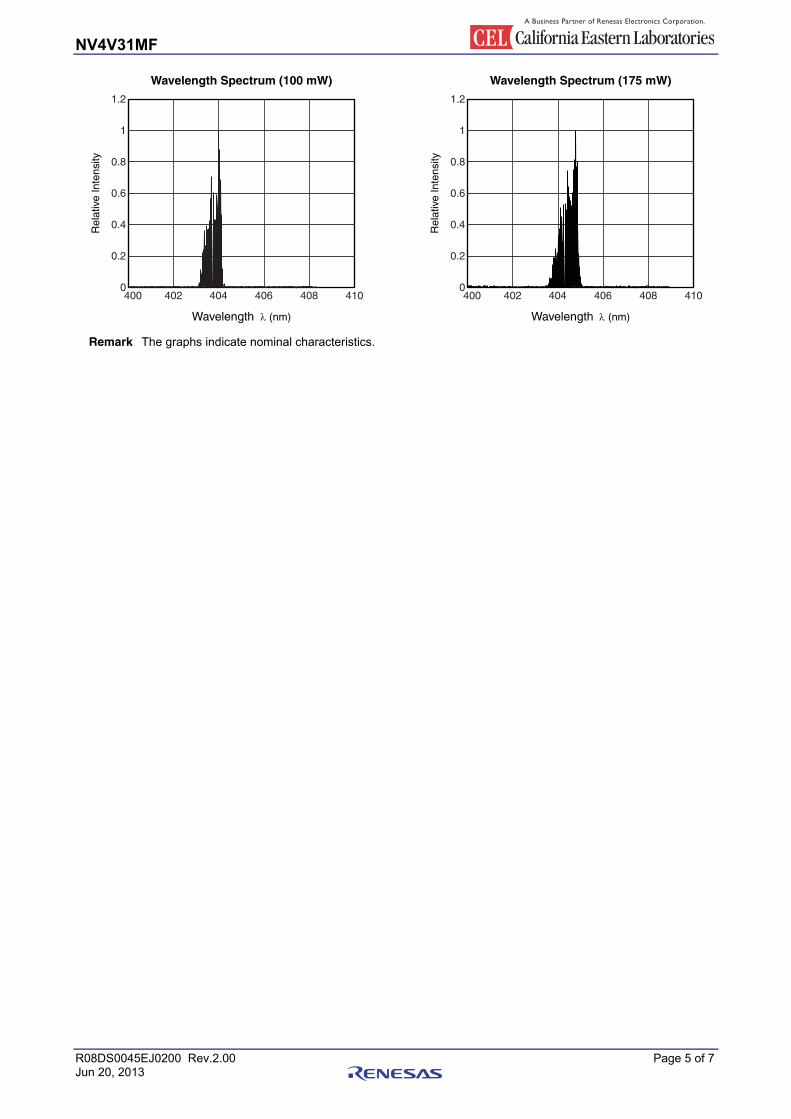
400 402 404 406 408 410
Wavelength Spectrum (100 mW)
Wavelength λ (nm)
Rel
ativ
e In
tens
ity
0
1.2
1
0.8
0.6
0.4
0.2
400 402 404 406 408 410
Wavelength Spectrum (175 mW)
Wavelength λ (nm)
Rel
ativ
e In
tens
ity
0
1.2
1
0.8
0.6
0.4
0.2
Remark The graphs indicate nominal characteristics.
A Business Partner of Renesas Electronics Corporation.

NV4V31MF
R08DS0045EJ0200 Rev.2.00 Page 6 of 7 Jun 20, 2013
NOTES ON HANDLING 1. Recommended soldering conditions
• Peak Temperature ≤ 350°C• Time ≤ 3 seconds• Soldering of leads should be made at the point 2.0 mm from the root of the lead• This device cannot be mounted using reflow soldering.
2. Usage cautions(1) Take the following steps to ensure that the device is not damaged by static electricity.
• Wear an antistatic wrist strap when soldering the device.We recommend a strap with a 1 MΩ resistor.
• Make sure that the work table and soldering iron are grounded.• Make sure that the soldering iron does not leak.
(2) Do not subject the package to undue stress.The package has a tensile strength of 1N or less.Do not exceed this rating. Also, avoid bending the leads as much as possible.If the leads must be bent, bend them only once, making sure to anchor the stem base of the lead.
(3) Do not allow the cap glass of the package to become scratched or dirty.Also, do not subject the cap glass to external force.
(4) Be sure to attach a heat sink to sufficiently dissipate heat.
(5) Use the device as soon as possible after opening the bag.
<R>
A Business Partner of Renesas Electronics Corporation.

NV4V31MF Chapter Title
R08DS0045EJ0200 Rev.2.00 Page 7 of 7 Jun 20, 2013
SAFETY INFORMATION ON THIS PRODUCT
DANGERVISIBLE LASER RADIATIONAVOID EYE OR SKIN EXPOSURE TODIRECT OR SCATTERED RADIATION
OUTPUT POWER 3W MAXWAVELENGTH 400 to 680nmCLASS IV LASER PRODUCT
AVOID EXPOSURE-InvisibleLaser Radiation is emitted fromthis aperture
SEMICONDUCTOR LASER
Warning Laser Beam A laser beam is emitted from this diode during operation. If the laser beam or its reflection enters your eye, it may cause injury to the eye or loss of eyesight. (Note that, depending on the wavelength of the beam, the laser beam might not be visible.)
• Do not look directly into the laser beam.
• Avoid exposure to the laser beam, any reflected or collimated beam.
<R>
A Business Partner of Renesas Electronics Corporation.

All trademarks and registered trademarks are the property of their respective owners.
C - 1
Revision History NV4V31MF Data Sheet
Description Rev. Date Page Summary0.01 Sep 08, 2011 − First edition issued 1.00 Mar 05, 2012 Throughout Preliminary Data Sheet -> Data Sheet
p.3 Modification of ORDERING INFORMATION p.4, 5 Addition of TYPICAL CHARACTERISTICS
2.00 Jun 20, 2013 p.1 Modification of FEATURES p.2 Modification of PACKAGE DIMENSIONS p.3 Modification of ORDERING INFORMATION
Modification of ABSOLUTE MAXIMUM RATINGS p.4 Modification of TYPICAL CHARACTERISTICS p.6 Modification of NOTES ON HANDLING p.7 Modification of SAFETY INFORMATION ON THIS PRODUCT

NOTICE
1. Descriptions of circuits, software and other related information in this document are provided only to illustrate the operation of semiconductor products andapplication examples. You are fully responsible for the incorporation of these circuits, software, and information in the design of your equipment. CaliforniaEastern Laboratories and Renesas Electronics assumes no responsibility for any losses incurred by you or third parties arising from the use of these circuits, software, or information.
2. California Eastern Laboratories has used reasonable care in preparing the information included in this document, but California Eastern Laboratories doesnot warrant that such information is error free. California Eastern Laboratories and Renesas Electronics assumes no liability whatsoever for any damagesincurred by you resulting from errors in or omissions from the information included herein.
3. California Eastern Laboratories and Renesas Electronics do not assume any liability for infringement of patents, copyrights, or other intellectual propertyrights of third parties by or arising from the use of Renesas Electronics products or technical information described in this document. No license, express,implied or otherwise, is granted hereby under any patents, copyrights or other intellectual property rights of California Eastern Laboratories or RenesasElectronics or others.
4. You should not alter, modify, copy, or otherwise misappropriate any Renesas Electronics product, whether in whole or in part. California EasternLaboratories and Renesas Electronics assume no responsibility for any losses incurred by you or third parties arising from such alteration, modification, copyor otherwise misappropriation of Renesas Electronics product.
5. Renesas Electronics products are classified according to the following two quality grades: “Standard” and “High Quality”. The recommended applicationsfor each Renesas Electronics product depends on the product’s quality grade, as indicated below. “Standard”: Computers; office equipment; communicationsequipment; test and measurement equipment; audio and visual equipment; home electronic appliances; machine tools; personal electronic equipment; and industrial robots etc. “High Quality”: Transportation equipment (automobiles, trains, ships, etc.); traffic control systems; anti-disaster systems; anti-crime systems; and safety equipment etc. Renesas Electronics products are neither intended nor authorized for use in products or systems that may pose a direct threat to human life or bodily injury (artificial life support devices or systems, surgical implantations etc.), or may cause serious property damages (nuclearreactor control systems, military equipment etc.). You must check the quality grade of each Renesas Electronics product before using it in a particularapplication. You may not use any Renesas Electronics product for any application for which it is not intended. California Eastern Laboratories and RenesasElectronics shall not be in any way liable for any damages or losses incurred by you or third parties arising from the use of any Renesas Electronics productfor which the product is not intended by California Eastern Laboratories or Renesas Electronics.
6. You should use the Renesas Electronics products described in this document within the range specified by California Eastern Laboratories, especially with respect to the maximum rating, operating supply voltage range, movement power voltage range, heat radiation characteristics, installation and other productcharacteristics. California Eastern Laboratories shall have no liability for malfunctions or damages arising out of the use of Renesas Electronics productsbeyond such specified ranges.
7. Although Renesas Electronics endeavors to improve the quality and reliability of its products, semiconductor products have specific characteristics such as the occurrence of failure at a certain rate and malfunctions under certain use conditions. Further, Renesas Electronics products are not subject to radiationresistance design. Please be sure to implement safety measures to guard them against the possibility of physical injury, and injury or damage caused by fire in the event of the failure of a Renesas Electronics product, such as safety design for hardware and software including but not limited to redundancy, fire control and malfunction prevention, appropriate treatment for aging degradation or any other appropriate measures. Because the evaluation ofmicrocomputer software alone is very difficult, please evaluate the safety of the final products or systems manufactured by you.
8. Please contact a California Eastern Laboratories sales office for details as to environmental matters such as the environmental compatibility of each Renesas Electronics product. Please use Renesas Electronics products in compliance with all applicable laws and regulations that regulate the inclusion or use of controlled substances, including without limitation, the EU RoHS Directive. California Eastern Laboratories and Renesas Electronics assume no liability for damages or losses occurring as a result of your noncompliance with applicable laws and regulations.
9. Renesas Electronics products and technology may not be used for or incorporated into any products or systems whose manufacture, use, or sale is prohibited under any applicable domestic or foreign laws or regulations. You should not use Renesas Electronics products or technology described in this document for any purpose relating to military applications or use by the military, including but not limited to the development of weapons of mass destruction. Whenexporting the Renesas Electronics products or technology described in this document, you should comply with the applicable export control laws and regulations and follow the procedures required by such laws and regulations.
10. It is the responsibility of the buyer or distributor of California Eastern Laboratories, who distributes, disposes of, or otherwise places the Renesas Electronicsproduct with a third party, to notify such third party in advance of the contents and conditions set forth in this document, California Eastern Laboratories andRenesas Electronics assume no responsibility for any losses incurred by you or third parties as a result of unauthorized use of Renesas Electronics products.
11. This document may not be reproduced or duplicated in any form, in whole or in part, without prior written consent of California Eastern Laboratories.12. Please contact a California Eastern Laboratories sales office if you have any questions regarding the information contained in this document or Renesas
Electronics products, or if you have any other inquiries.
NOTE 1: “Renesas Electronics” as used in this document means Renesas Electronics Corporation and also includes its majority-owned subsidiaries.NOTE 2: “Renesas Electronics product(s)” means any product developed or manufactured by or for Renesas Electronics.NOTE 3: Products and product information are subject to change without notice.
CEL Headquarters • 4590 Patrick Henry Drive, Santa Clara, CA 95054 • Phone (408) 919-2500 • www.cel.com
For a complete list of sales offices, representatives and distributors,Please visit our website: www.cel.com/contactus