numerical and experimental study of the thermal stress of silicon induced by a millisecond laser
TRANSCRIPT

Numerical and experimental study of the thermalstress of silicon induced by a millisecond laser
Xi Wang, Yuan Qin, Bin Wang, Liang Zhang, Zhonghua Shen, Jian Lu, and Xiaowu Ni*School of Science, Nanjing University of Science &Technology, Nanjing 210094, China
*Corresponding author: [email protected] (Xiaowu Ni)
Received 10 January 2011; revised 27 March 2011; accepted 27 March 2011;posted 30 March 2011 (Doc. ID 140893); published 11 July 2011
A spatial axisymmetric finite element model of single-crystal silicon irradiated by a 1064nmmillisecondlaser is used to investigate the thermal stress damage induced by a millisecond laser. The transienttemperature field and the thermal stress field for 2ms laser irradiation with a laser fluence of254J=cm2 are obtained. The numerical simulation results indicate that the hoop stresses along the raxis on the front surface are compressive stress within the laser spot and convert to tensile stress outsidethe laser spot, while the radial stresses along the r axis on the front surface and on the z axis are com-pressive stress. The temperature of the irradiated center is the highest temperature obtained, yet thestress is not always highest during laser irradiation. At the end of the laser irradiation, themaximal hoopstress is located at r ¼ 0:5mm and the maximal radial stress is located at r ¼ 0:76mm. The temperaturemeasurement experiments are performed by IR pyrometer. The numerical result of the temperature fieldis consistent with the experimental result. The damage morphologies of silicon under the action of a254J=cm2 laser are inspected by optical microscope. The cracks are observed initiating at r ¼ 0:5mmand extending along the radial direction. © 2011 Optical Society of AmericaOCIS codes: 140.3330, 040.6040.
1. Introduction
The study of laser–semiconductor interactionmechanisms has been a very active field over theyears and has attracted more interest recently. Semi-conductors are the substrate material in photodetec-tor and IR systems. Silicon and germanium havehigh transmissivity in the IR band (1 μm–12 μm).Moreover, silicon material has high transmissivityin the far-IR band (300 μm–3000 μm). As IR windowmaterials, they have wide applications in IR imagingsystems and IR filters. Photodetector and IR imagingsystems are subjected to being damaged and inter-fered with in optics-electronic countermeasure.Therefore, it is important to study the damage me-chanism of photodetectors induced by lasers, whichalso can contribute to the study of laser–semiconduc-tor interaction mechanisms. Some damage effectsare induced by laser irradiation, such as melting
damage, thermal stress damage, optical breakdown,and avalanche ionization, in which the thermalstress effect is one of the most important damagemechanisms. Accordingly, as a typical semiconductormaterial, silicon is significant to study for its thermalstress distribution and thermal stress damage underlaser irradiation.
The studies of laser–silicon interaction have beenmuch investigated in past years. Nevertheless, mostof the research has been devoted to the femtosecondlaser, nanosecond laser, and cw laser [1–3]. Up tonow, very few studies relate to the thermal stressdamage induced by millisecond lasers. In the inves-tigation of Conde et al., amorphous silicon and ger-manium films were deposited on silicon wafers [4].They obtained the temperature distribution and thethermal stress time evolution induced by a 20nslaser using the finite element method. A fluence of0:18 J=cm2 is enough to reach the melting point onthe interface of the amorphous silicon and germa-nium films. Many studies only considered siliconas a brittle material at room temperature and
0003-6935/11/213725-08$15.00/0© 2011 Optical Society of America
20 July 2011 / Vol. 50, No. 21 / APPLIED OPTICS 3725

ignored the plastic character of silicon at high tem-peratures. This is a special characteristic of silicondue to the fact that the plastic behavior is correlatedclosely with the temperature. It changes from brittlebehavior to more plastic behavior at temperaturesbetween 790 and 920K [5]. Zhang and Zarudipointed out that the mechanism of plasticity insilicon is complex, involving dislocations, phasetransformation, and chemical reactions [6]. The plas-tic character of silicon has been presented in otherstudies [7,8]. Gross et al. suggested two models toexplain crack initiation and the patterns of cracksduring the laser cutting of silicon [7]. They observedthat radial cracks arrest at the deformed zone bound-ary whereas circumferential cracks follow thedeformed zone boundary. Cheng et al. [8] experimen-tally proposed that the strong dislocation activityand plastic deformation could be generated in siliconcrystal by the heat-assisted laser shock peeningprocess.
The studies mentioned above concentrated onfemtosecond lasers, nanosecond lasers or cw lasers,and only a few related to millisecond lasers. Airbreakdown and plasma will be generated due tothe high peak power density during the conventionalnanosecond and femtosecond laser interaction withmaterials. The energy is then shielded and wastedduring the long-distance transmission process. Thereare some distinctive features of millisecond lasers,such as longer pulse width, larger pulse energyand high efficiency of energy coupling [9]. In the pre-sent study, a spatial axisymmetric finite elementmodel (FEM) of silicon irradiated by a single-pulsemillisecond laser is used. We take into considerationthe nonlinear change of the thermal and the mechan-ical parameters with temperature. The temperatureof elastic-plastic deformation (790 –920K) for siliconis lower than the melting point (1685K). Therefore,the plastic character of silicon in the high tempera-ture condition is considered in our calculation. Thethermal stresses of silicon are investigated in orderto assess which stresses are generated and predictwhere the cracks occur first. The temperaturemeasurement experiments are performed to verifythe numerical simulation results of the temperature.The damage morphologies of silicon induced bydifferent laser fluences are observed.
2. Mathematical Model and FEM
A. Mathematical Model
The two-dimensional FEM is illustrated schemati-cally in Fig. 1, in which a cylindrical coordinatesystem is adopted. The incident laser beam is per-pendicular to the surface of the sample. The lengthand the thickness of the silicon are b and h, respec-tively. Axis z is the symmetry axis, r is the radialdirection, and O is the center point of the frontsurface. To make the problem simpler, some assump-tions are made, as follows: (1) the material is homo-geneous and isotropic; (2) the sample is large enough
so that the heat energy will not transfer to the bound-ary during laser irradiation; (3) the temperature atinfinity is room temperature along the r and z direc-tions; (4) the thermal losses by convection and radia-tion of the silicon surface are ignored. The thermalconduction equation can be described as
ρc ∂Tðr; z; tÞ∂t
¼ 1r∂
∂r
�rk
∂Tðr; z; tÞ∂r
�
þ ∂
∂z
�k∂Tðr; z; tÞ
∂z
�þ q; ð1Þ
where Tðr; z; tÞ represents the instantaneous tem-perature at ðr; z; tÞ, and ρ, c, and k are the density,specific heat, and thermal conductivity, respectively.In addition, q is the volumetric heat source which isdescribed by
q ¼ I0ð1 −RÞαf ðrÞgðtÞ expð−αzÞ; ð2Þwhere I0 is the incident laser peak power density atthe laser spot center, R and α are the surface reflec-tivity and the optical absorption coefficient, and f ðrÞand gðtÞ are the spatial and temporal distribution ofthe laser beam. The incident laser beam is assumedto be of Gaussian distribution. For a TEM00 modelaser, they can be written as
f ðrÞ ¼ exp�−2r2
a20
�;
gðtÞ ¼ 1;
Iðr; tÞ ¼ I0 exp�−2r2
a20
�; ð3Þ
where a0 is the 1=e2 of the intensity radius of theGaussian beam.
The boundary conditions are
−k∂Tðr; z; tÞ
∂z
����z¼h
¼ −k∂Tðr; z; tÞ
∂r
����r¼b
¼ 0: ð4Þ
The initial condition is
Tðr; z; tÞjt¼0 ¼ T0: ð5Þ
Fig. 1. Schematic diagram of the silicon sample irradiated bylaser. O, center point of the front surface; r, the radial direction,z axis, symmetry axis, b and h, length and the thickness of thesample, respectively.
3726 APPLIED OPTICS / Vol. 50, No. 21 / 20 July 2011

T0 is the room temperature, which is taken as300K. No heat flux transfer occurs along the radialdirection on the z axis in the axisymmetric model,thus
−k∂Tðr; z; tÞ
∂r
����r¼0
¼ 0: ð6Þ
B. Calculation Methods
1. Solving the Temperature Field
According to Eqs. (1)–(5), the FEM controllingequation for temperature can be written as
½C�f _Tg þ ½K th�fTg ¼ fQg; ð7Þ
where ½C�; f _Tg; ½K th�; fTg are the heat capacitymatrix, temperature rise rate vector, heat conductionmatrix, and temperature vector, respectively. f _Tg ¼dfTg=dt. The absorbed laser energy is expressed bythe heat source vector fQg. The Crank–Nicolsonmethod [10,11] is used to solve Eq. (7), and the tem-poral discrete form of Eq. (7) can be derived:
�1Δt
½C� þ θ½K th��fTgt ¼
�1Δt
½C� − ð−θÞ½K th��fTgtþΔt
þ θfQgt þ ð1 − θÞfQgtþΔt; ð8Þ
where Δt is the time interval and θ ¼ 1=2.
2. Solving the Thermal Stress Field
The stress–strain relationship is linear in the elasticregion and converts to nonlinear in the plastic region.The strain is related to the current stress and theload history. The increment method is employed.The temperature increments can be taken as load in-crements at every node. The thermal stress can beobtained from the thermal elastoplastic constitutivetheory and VonMises yield criterion [12]. The stress–strain relation is given by the following equation [13]:
fΔσg ¼ ½D�epfΔεg; ð9Þ
where fΔσg and fΔεg are the total stress incrementand strain increment of the element and ½D�ep is theelastoplastic matrix.
In the elastic region, fΔεg ¼ fΔεge þ fΔεgT , wherefΔεge and fΔεgT are the elastic strain incrementand the thermal strain increment vector. fΔεgT ¼fαgfΔTg, where fαg is the thermal expansion coeffi-cient vector and fΔTg ¼ fTgtþΔt − fTgt is the tem-perature increment vector. fΔσg can be described as
fΔσg ¼ ½D�eðfΔεg − fΔεgT −∂½D�−1e∂T
fσgdTÞ; ð10Þ
where ½D�e is the elastic matrix,
½D�e ¼E
ð1þ μÞð1− 2μÞ
26641− μ μ μ 0μ 1− μ μ 0μ μ 1− μ 00 0 0 ð1− 2μÞ=2
3775;
where E and μ are the Young’s modulus andPoisson’s ratio, respectively.
In the plastic region, the total strain increment isfΔεg ¼ fΔεge þ fΔεgT þ fΔεgP, where fΔεgp is theplastic strain increment of the element. The stress–strain relation can be described finally as
fΔσg ¼ ½D�ep�fΔεg − fΔεgT −
∂½D�−1e∂T
fσgdT�
þ½D�e ∂ �σ
∂fσg∂H0∂T dT
H0 þ�
∂ �σ∂fσg
�T½D�e ∂ �σ
∂fσg
; ð11Þ
where ½D�ep is the elastoplastic matrix,
½D�ep ¼ ½D�e −½D�e ∂ �σ
∂fσg
�∂ �σ∂fσg
�T½D�e
H 0 þ�
∂ σ∂fσg
�T½D�e ∂ �σ
∂fσg
;
and H0 is the hardness modulus.The nodal temperature load increment from t to
tþΔt is transformed to be the nodal force load incre-ment. The incremental strain from the constitutiveequation Eq. (9) is written as
fΔσg ¼ ½D�epð½B�fΔUg − fΔεgTÞ; ð12Þ
where ½B� is the geometric matrix and fΔUg is thedisplacement increment vector. The nodal elementload increment induced by the change of tempera-ture fΔRgtþΔt can be represented as
fΔRgtþΔt ¼ZZe
½B�T ½D�epfΔεgT2πrdrdz: ð13Þ
The finite element increment equation at time tþΔt is described by
½K�tþΔtfΔUg ¼ fΔRg; ð14Þ
where ½K � is the general stiffness matrix.According to the total equilibrium equation, the
displacement increment fΔUg is first calculatedfrom Eq. (14). Substituting fΔUg into Eq. (12), thestress increment of element Δσ is obtained. Thestress results of every time step are then obtained.The Newton–Raphson iteration method is employedin our calculations.
20 July 2011 / Vol. 50, No. 21 / APPLIED OPTICS 3727

C. Material Parameters
We calculated the temperature field and the thermalstress field of silicon irradiated by a 2ms laser with afluence of 254 J=cm2. The initial temperature is300K, the laser spot radius is 500 μm, and thesample size is 10mm × 1mm. The melting point ofsilicon is 1685K, the density ρ ¼ 2330kg=m3, andthe Poisson’s ratio is 0.27; other thermal and me-chanism parameters used are listed in Table 1[14–17]. Most of the parameters vary with tempera-ture. Especially the yield strength, compressivestrength, and tensile strength, which decreasestrongly with the temperature. During the solid-liquid phase transition process, the temperatureremains constant at the melting point. The absorbedor emitted energy is the phase latent heat changewhich is considered the enthalpy. The enthalpy iswritten as H ¼ R
ρCðTÞdT. The melting latent heatof silicon is 1800 J=g.
3. Numerical Results and Experimental Results
A. Temperature Field Results
According to Eqs. (1)–(8), the numerical results ofthe temperature field were obtained. To verify thenumerical simulation results of temperature, anexperimental temperature measurement was per-formed. The experiment setup is illustrated in Fig. 2.A 1064nm Nd:YAG laser system, Melar-50 fromBeamtech Optronics Co., Ltd., China (minimal pulsewidth of 0:5ms, maximal pulse width of 2:5ms, andmaximal energy of 50 J), was used in the experiment.The mode of the millisecond laser beam was TEM00with Gaussian spatial distribution, and the beamdivergence angle was less than 3mrad. An IR pyrom-eter KMGA740 from Kleiber Infrared GmbH (re-sponse time of 6 μs, minimal sampling intervaltime of 10 μs, spectral range of 2:0 μm–2:5 μm, andtemperature measuring range of 623–3773K) wasused to measure the temperature of the siliconsurface. In our experiment, the pulse width wasτ ¼ 2ms. The energy meter took real-time measure-ments of the incident laser energy. The output laserbeam was focused by an f ¼ 100mm lens and irra-diated the surface of the sample. To define the laserspot radius of 500 μm, the sample was located at adefocused distance of 5mm rather than at the focus.We adjusted the laser energy density by controllingthe laser energy and inserting an attenuator in thebeam path. A h100i single-crystal silicon wafer(20mm × 10mm × 1mm) was positioned on a three-
dimensional precision displacement platform. Thesilicon was initially polished and cleaned in isopropylalcohol and deionized water, then dipped into diluteHF to remove the oxide layer on its surface, andfinally rinsed in the deionized water.
The temperature evolution of the laser spot centerunder the action of the 254 J=cm2 laser is presentedin Fig. 3. The laser pulse width is τ ¼ 2ms. The solidline represents the experimental result, and thedotted line represents the numerical simulationresult. The silicon material absorbs the laser energyso that the temperature rises rapidly during the time0ms–2ms, and then cools down after 2ms. For theexperimental result, the temperature reaches themelting point 1685K at t ¼ 1:09ms. The peak tem-perature is 1788K at t ¼ 2ms. For the calculationresult, the temperature reaches the melting point1685K at t ¼ 1:14ms, and the peak temperature isup to 1803K at t ¼ 2ms. After 2ms, it cools downgradually to room temperature, 300K. The tempera-ture evolution in the calculation result is similar tothe experimental result. The relative error of thetemperature value between the experimental resultand the calculation result is less than 5%. The errorhas two parts. It includes calculation error andexperimental error. The calculation error can beattributed to the fact that we ignored the thermalradiation and the thermal convection in the calcula-tions. The experimental error is due to the fact thatthe emissivity of silicon is set as constant in the IRpyrometer. In fact, the emissivity of silicon varieswith temperature [18]. In addition, a plateau existsin the curve of the experimental result as well as inthe curve of the numerical simulation result. Theplateaus in Fig. 3 represent the solid–liquid phasechange process. The temperature remains almostconstant at the melting point during the solid–liquidphase change. The absorption coefficient of solid-state silicon and liquid-state silicon are 50 cm−1 and8:6 × 105 cm−1, respectively [14]. Thus, the optical
Fig. 2. Experiment setup for the temperature measurements.1064nm Gaussian pulse laser is operating at TEM00 mode, laserpulse width τ ¼ 2ms, laser spot radius is 500 μm, energy densityE ¼ 254J=cm2. Measure range of infrared pyrometer KMGA740 is623K-3773K.
Table 1. Thermal and Mechanical Parameters of Silicon
Temperature (K) 300 573 773 973 1173 1373 1573 1873
Specific heat(J=ðKg · KÞ) 712.16 825.19 885.67 916.5 980.29 1005.47 1027.24 1056.97Thermal conductivity (ðW=m · KÞ) 156 64 43 31 26 24 23 19Linear expansibility (ð10−6 · K−1Þ 2.616 3.842 4.151 4.258 4.384 4.5 4.612 4.78Young’s modulus (GPa) 130.56 122.53 116.64 110.75 104.87 90.9 89.6 ————
Yield strength (MPa) 5540 4530 1780 61 8 3 0.5 ————
3728 APPLIED OPTICS / Vol. 50, No. 21 / 20 July 2011

absorption coefficient of the liquid-state Si isapproximately 4 orders of magnitude higher thanthat of the solid-state Si. Consequently, the tempera-ture gradient in the liquid state is sharper than inthe solid state.
The temperature of the silicon sample along the rdirection and the z direction at different times areshown in Figs. 4 and 5. In Fig. 4, it can be seen thatthe temperature on the front surface decreasesgradually along the r direction at the same time. Thetemperature distribution shows a similar featurewith the spatial distribution of the Gaussian beam.It indicates that the temperature distribution alongthe r direction is related to the spatial distribution ofthe incident laser beam. At 2ms, the temperature atthe spot center exceeds the melting point andreaches 1803K. The plateau in the 2ms curve showsthat the melting region extends to r ¼ 0:18mm. Asshown in Fig. 5, the temperatures decrease alongthe z direction. According to the Beer–Lambertlaw, I ¼ I0 expð−αzÞ, where I0 is the intensity of theincident beam, I is the intensity of the transmittedbeam, and α is the absorption coefficient. When
the incident beam irradiates the sample perpendicu-larly, the absorbed energy decreases exponentiallywith increasing depth below the surface. Conse-quently, the temperatures decrease exponentiallyfollowing the Beer–Lambert law in the depth direc-tion. The plateau in Fig. 5 reveals that the meltingdepth in the silicon sample is 0:1mm.
B. Thermal Stress Field Results from Calculations
The temperature increase in the irradiated arearesults in great thermal expansion and a steep tem-perature gradient. At the same time, the continuityof the material impedes its free expansion. There-fore, thermal stresses will arise. Once the maximumthermal stress exceeds the critical stress, thermalstress damage will be generated. The criticalstrength of silicon decreases with increasing tem-perature. Therefore, the probability of the cracks’occurrence during the cooling periods is smaller thanthat during the laser irradiation process. Thus wecalculated the thermal stress distribution duringthe laser irradiation.
On the one hand, the thermal stress increasesrapidly as a result of temperature rise and thermalexpansion. On the other hand, the mechanicalparameters (Young’s modulus, yield strength) ofsilicon decrease severely with increasing tempera-ture, which is the so-called thermal softening effect.The thermal stress will decrease due to the thermalsoftening effect. The Von Mises stress in the centeron the front surface is shown is Fig. 6. It can be seenthat the Von Mises stress in the center reaches themaximum value of 120MPa at 0:568ms and thendecreases after 0:568ms. The stresses approach zeroafter 1:14ms. This is because the plastic yield occursat 0:568ms and the temperature in the centerreaches the melting point at 1:14ms. The plasticyield will occur once the Von Mises stress exceedsthe yield strength. The temperature in the centeris highest, but the corresponding yield strength islowest; therefore, the plastic yield occurs in thecenter first. As shown in Fig. 3, the temperature
Fig. 4. (Color online) Temperature along r direction on thefront surface at different times of Si sample obtained fromcalculations.
Fig. 5. (Color online) Temperature along z direction (r ¼ 0) atdifferent times of Si sample obtained from calculations.
Fig. 3. (Color online) Temperature time evolution of the laserspot center at laser fluence of 254J=cm2 of Si sample.
20 July 2011 / Vol. 50, No. 21 / APPLIED OPTICS 3729
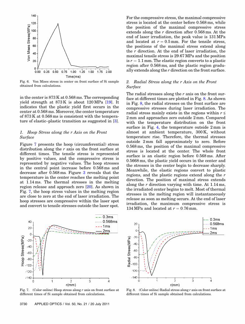
in the center is 873K at 0:568ms. The correspondingyield strength at 873K is about 120MPa [19]. Itindicates that the plastic yield first occurs in thecenter at 0:568ms. Moreover, the center temperatureof 873K at 0:568ms is consistent with the tempera-ture of elastic–plastic transition as suggested in [3].
1. Hoop Stress along the r Axis on the FrontSurface
Figure 7 presents the hoop (circumferential) stressdistribution along the r axis on the front surface atdifferent times. The tensile stress is representedby positive values, and the compressive stress isrepresented by negative values. The hoop stressesin the central point increase before 0:568ms anddecrease after 0:568ms. Figure 3 reveals that thetemperature in the center reaches the melting pointat 1:14ms. The thermal stresses in the meltingregion release and approach zero [20]. As shown inFig. 7, the hoop stress values in the melting regionare close to zero at the end of laser irradiation. Thehoop stresses are compressive within the laser spotand convert to tensile stresses outside the laser spot.
For the compressive stress, the maximal compressivestress is located at the center before 0:568ms, whilethe position of the maximal compressive stressextends along the r direction after 0:568ms. At theend of laser irradiation, the peak value is 131MPaand located at r ¼ 0:5mm. For the tensile stress,the positions of the maximal stress extend alongthe r direction. At the end of laser irradiation, themaximal tensile stress is 29:67MPa and the positionis r ¼ 1:1mm. The elastic region converts to a plasticregion after 0:568ms, and the plastic region gradu-ally extends along the r direction on the front surface.
2. Radial Stress along the r Axis on the FrontSurface
The radial stresses along the r axis on the front sur-face at different times are plotted in Fig. 8. As shownin Fig. 8, the radial stresses on the front surface arecompressive stresses during laser irradiation. Theradial stress mainly exists in the regions within r ≤2mm and approaches zero outside 2mm. Comparedwith the temperature distribution on the frontsurface in Fig. 4, the temperature outside 2mm isalmost at ambient temperature, 300K, withouttemperature rise. Therefore, the thermal stressesoutside 2mm fall approximately to zero. Before0:568ms, the position of the maximal compressivestress is located at the center. The whole frontsurface is an elastic region before 0:568ms. After0:5668ms, the plastic yield occurs in the center andthe stresses in the center begin to decrease sharply.Meanwhile, the elastic regions convert to plasticregions, and the plastic regions extend along the rdirection. The position of maximal stress extendsalong the r direction varying with time. At 1:14ms,the irradiated center begins to melt. Most of thermalstresses in the melting region will instantaneouslyrelease as soon as melting occurs. At the end of laserirradiation, the maximum compressive stress is134MPa and located at r ¼ 0:76mm.
Fig. 7. (Color online) Hoop stress along r axis on front surface atdifferent times of Si sample obtained from calculations.
Fig. 8. (Color online) Radial stress along r axis on front surface atdifferent times of Si sample obtained from calculations.
Fig. 6. Von Mises stress in center on front surface of Si sampleobtained from calculations.
3730 APPLIED OPTICS / Vol. 50, No. 21 / 20 July 2011

3. Radial Stress Distribution along the z Axis
The radial stress distributions along the z axis atdifferent times are illustrated in Fig. 9. The radialstresses are equal to the hoop stresses on thesymmetry axis (z axis). The lower temperatureregions block the thermal expansion from the highertemperature regions. Therefore, the radial stress iscompressive on the z axis. At the same time, theradial stresses first increase and then decrease alongthe depth direction. The elastic region converts to theplastic region after 0:568ms, and the plastic regionextends along the z axis. The position of maximalstress is not located in the center during the laserirradiation. It propagates along the inner depth onthe symmetry axis as time progresses. At the end oflaser irradiation, the maximum stress is 243MPaand located at z ¼ 0:37mm. The radial stress in themelting region releases and approaches zero.
C. Experiment and Correlation to Simulations
The damages to silicon morphology induced by differ-ent laser fluences were inspected using an opticalmicroscope.Theexperimental setup is showninFig.2.The laser pulse width τ ¼ 2ms, and the laser spot ra-dius is 500 μm. The damage morphology is presentedin Fig. 10. Wemainly observed the shapes and the in-itiation positions of the cracks. Figure 10(a) shows thedamage morphology induced by a laser of 229 J=cm2.It can be seen there that the surface layer has alreadymelted but there are no cracks observed at the bound-ary of themelting region. Figure 10(b) shows themor-phology damage induced by a laser of 254 J=cm2, inwhich melting damage and thermal stress damageboth occur. Two radial cracks are observed at theboundary of the melting region. The cracks (markedwith arrows) initiate at r ¼ 0:5mm and grow alongthe radial direction.
The hoop stress distribution in Fig. 7 indicates thatthe maximal hoop compressive stress is located atr ¼ 0:5mm. The center region has melted, and mostof the stresses are released. The compressive stres-ses convert to tensile stress outside the laser spot.
The maximal hoop tensile stress is located at r ¼1:1mm. If the compressive (tensile) stress is equalto or exceeds the compressive (tensile) strength, ther-mal stress damage will occur. The crack will startfrom the position of maximal stress. The crack underthe action of hoop stress will propagate along the ra-dial direction [7]. We deduce that the cracks initiatefrom r ¼ 0:5mm and then grow along the radial di-rection under the action of tensile stress. The experi-mental result in Fig. 10(b) shows that the cracks firstinitiate at r ¼ 0:5mm and propagate along the radialdirection. The crack initiation position in the experi-ment is consistent with the calculation position of themaximal stress.
As described in our previous study, the circumfer-ential crack is observed outside the laser spot on thefront surface [21]. The radial stress distribution inFig. 8 reveals that the maximum radial stress islocated at r ¼ 0:76mm. The incident laser spotradius is 0:5mm in our calculation. The maximumradial stress is located outside the laser spot. Thecrack grows along the circumferential direction un-der the action of radial stress [22]. We deduce thatthe circumferential crack is located outside the laserspot. The circumferential crack [21] exhibits thesame trend with our calculation.
Fig. 9. (Color online) Radial stress on the z-axis at different timesof the Si sample obtained from calculations.
Fig. 10. (Color online) Damage morphology of silicon sample in-duced by a single pulse laser at different energy densities. Laserpulse width τ ¼ 2ms. (a) Damage morphology at a laser fluence of229J=cm2; surface layer melting without thermal stress damage.(b) Damage morphology at a laser fluence of 254J=cm2; meltingdamage and thermal stress damage both occur. The cracks initiateat r ¼ 05mm and propagate along the radial direction.
20 July 2011 / Vol. 50, No. 21 / APPLIED OPTICS 3731

4. Conclusions
FEM is applied to calculate the temperature andthermal stress distribution on silicon induced by amillisecond laser based on the thermoelastic–plastictheory. A temperature measurement experiment wascarried out to verify the numerical simulation resultsof a temperature field and to compare to the numer-ical calculation model. The results indicate that thehoop stress within the laser spot radius is a compres-sive stress and converts to a tensile stress outside thelaser spot. Themaximal compressive stress is locatedat the boundary of the laser spot. The radial stress onthe front surface is a compressive stress. The maxi-mal radial stress is located outside the laser spot.The radial stress along the z axis is a compressivestress. The temperature at the center is highest,but the stress is not always highest there throughoutthe laser irradiation process. We assume that theradial crack first occurs at the boundary of the laserspot rather than at the center. The damage morphol-ogies of silicon under the action of different fluenceswere inspected to confirm the cracks’ numericalstress theory predictions. With a laser of 254 J=cm2,not only melting damage occurs but also thermalstress damage. It is observed that the cracks occuron the surface and extend along the radial direction.The crack initiation position is consistent with thesimulations.
The results in our study can provide a theoreticalfoundation for thermal stress damage in silicon andpredict what kind of stresses occur during millise-cond laser irradiation.
This work was supported by the NanjingUniversity of Science & Technology (NUST),Research Funding 2010ZYTS069.
Reference1. V. K. Arora and A. L. Dawar, “Laser-induced damage studies
in silicon and silicon-based photodetectors,” Appl. Opt. 35,7061–7065 (1996).
2. V. Zorba, N. Boukos, I. Zergioti, and C. Fotakis, “Ultravioletfemtosecond, picosecond, and nanosecond lasermicrostructur-ing of silicon: structural and optical properties,” Appl. Opt. 47,1846–1850 (2008).
3. X. R. Zhang and X. Xu, “High precision microscale bendingby pulsed and CW lasers,” J. Appl. Mech. 125, 512–518 (2003).
4. J. C. Conde, E. Martín, F. Gontad, S. Chiussi, L. Fornarini, andB. León, “Numerical analysis of temperature profile andthermal-stress during excimer laser induced heteroepitaxialgrowth of patterned amorphous silicon and germaniumbi-layer deposited on Si ð100Þ,” Thin Solid Films 518,2431–2436 (2010).
5. H. Exner and U. Loschnner, “Contactless laser bending ofsilicon microstructures,” Proc. SPIE 5116, 383–392 (2003).
6. L. Zhang and I. Zarudi, “Towards a deeper understanding ofplastic deformation in monocrystalline silicon,” Int. J. Mech.Sci. 43, 1985–1996 (2001).
7. T. S. Gross, S. D. Hening, and D. W. Watt, “Crack formationduring laser cutting of silicon,” J. Appl. Phys. 69, 983–989(1991).
8. G. J. Cheng, M. Cai, D. Pirzada, M. J. Guinel, and M. G.Norton, “Plastic deformation in silicon crystal induced byheat-assisted laser shock peening,” J. Manuf. Sci. Eng. 130,011008 (2008).
9. B. Wang, Y. Qin, X. W. Ni, Z. H. Shen, and J. Lu, “Effect ofdefects on long-pulse laser-induced damage of two kinds ofoptical thin films,” Appl. Opt. 49, 5537–5544 (2010).
10. J. Crank and P. Nicolson, “A practical method for numericalevaluation of solutions of partial differential equations ofthe heat-conduction type,” Proc. Cambridge Philos. Soc. 43,50–67 (1947).
11. J. Crank and P. Nicolson, “A practical method for numericalevaluation of solutions of partial differential equations ofthe heat-conduction type,” Reprinted in Adv. Comput. Math.6, 207–226 (1996).
12. Y. Chen, J. Lu, X. Ni, J. Bi, and X. Zhang, “Plastic penetrationduring laser heating of a metal plate,” J. Mater. Process. Tech-nol. 205, 9–15 (2008).
13. O. C. Zienkiewicz and R. L. Tayor, The Finite Element Method(Butterworth-Heinemann, 2000).
14. Semiconductors and Semimetals, R. F. Wood, C. W. White, andR. T. Young, eds., Vol. 23 of Pulsed Laser Processing of Semi-conductors (Academic, 1984).
15. R. Hull, Properties of Crystalline Silicon (INSPEC, 1999).16. H. Siethoff, H. G. Brion, andW. Schroter, “A regime of the yield
point of silicon at high temperature,” Appl. Phys. Lett. 75,1234–1236 (1999).
17. A. Fischer, H. Richter, A. Shalynin, P. Krottenthaler, G.Obermeier, U. Lambert, and R. Wahlich, “Upper yield pointof large diameter silicon,” Microelectron. Eng. 56, 117–122(2001).
18. N. M. Ravindra, K. Ravindra, S. Mahendra, B. Sopori, and A.T. Fiory, “Modeling and simulation of emissivity of silicon-related materials and structures,” J. Electron. Mater. 32,1052–1058 (2003).
19. J. Frühauf, E. Garther, and E. Jansch, “New aspects of theplastic deformation of silicon-prerequisites for the reshapingof silicon microelements,” Appl. Phys. A 68, 673–679 (1999).
20. J. F. Li, L. Li, and F. H. Stott, “Thermal stresses and theirimplication on cracking during laser melting of ceramicmaterials,” Acta Mater. 52, 4385–4398 (2004).
21. X. Wang, D. H. Zhu, Z. H. Shen, J. Lu, and X. W. Ni, “Surfacedamage morphology investigations of silicon under millise-cond laser irradiation,”Appl. Surf. Sci. 257, 1583–1588 (2010).
22. Y. Z. Yan, L. F. Ji, Y. Bao, and Y. J. Jiang, “Theory analysisand experiment verification on crack characters duringlaser processing ceramics,” Chin. J. Lasers 35, 1401–1408(2008).
3732 APPLIED OPTICS / Vol. 50, No. 21 / 20 July 2011