elimination of potential-induced degradation for ... of potential-induced degradation for...
TRANSCRIPT

Elimination of Potential-Induced Degradation for Crystalline Silicon Solar Cells
by
Jaewon Oh
A Dissertation Presented in Partial Fulfillment
of the Requirements for the Degree
Doctor of Philosophy
Approved July 2016 by the
Graduate Supervisory Committee:
Stuart Bowden, Co-Chair
Govindasamy Tamizhmani, Co-Chair
Christiana Honsberg
Peter Hacke
Dieter Schroder
ARIZONA STATE UNIVERSITY
December 2016

i
ABSTRACT
Potential-Induced Degradation (PID) is an extremely serious photovoltaic (PV)
durability issue significantly observed in crystalline silicon PV modules due to its rapid
power degradation, particularly when compared to other PV degradation modes. The
focus of this dissertation is to understand PID mechanisms and to develop PID-free cells
and modules.
PID-affected modules have been claimed to be fully recovered by high
temperature and reverse potential treatments. However, the results obtained in this work
indicate that the near-full recovery of efficiency can be achieved only at high irradiance
conditions, but the full recovery of efficiency at low irradiance levels, of shunt resistance,
and of quantum efficiency (QE) at short wavelengths could not be achieved. The QE loss
observed at short wavelengths was modeled by changing the front surface recombination
velocity. The QE scaling error due to a measurement on a PID shunted cell was addressed
by developing a very low input impedance accessory applicable to an existing QE system.
The impacts of silicon nitride (SiNx) anti-reflection coating (ARC) refractive
index (RI) and emitter sheet resistance on PID are presented. Low RI ARC cells (1.87)
were observed to be PID-susceptible whereas high RI ARC cells (2.05) were determined
to be PID-resistant using a method employing high dose corona charging followed by
time-resolved measurement of surface voltage. It has been demonstrated that the PID
could be prevented by deploying an emitter having a low sheet resistance (~ 60 /sq)
even if a PID-susceptible ARC is used in a cell. Secondary ion mass spectroscopy (SIMS)
results suggest that a high phosphorous emitter layer hinders sodium transport, which is
responsible for the PID. Cells can be screened for PID susceptibility by illuminated lock-

ii
in thermography (ILIT) during the cell fabrication process, and the sample structure for
this can advantageously be simplified as long as the sample has the SiNx ARC and an
aluminum back surface field.
Finally, this dissertation presents a prospective method for eliminating or
minimizing the PID issue either in the factory during manufacturing or in the field after
system installation. The method uses commercially available, thin, and flexible Corning®
Willow® Glass sheets or strips on the PV module glass superstrates, disrupting the
current leakage path from the cells to the grounded frame.

iii
To my God

iv
ACKNOWLEDGMENTS
Firstly, I would like to express my sincere gratitude to my co-advisors, Dr. Stuart
Bowden and Dr. Govindasamy Tamizhmani for their guidance, support, and patience.
Their guidance helped me in all the time of research. I really appreciate all their
contributions of time, ideas, and funding to make my Ph.D experience stimulating and
productive. I would also like to thank Dr. Peter Hacke at NREL for serving on my
committee member and valuable comments for my research. I would like to acknowledge
Dr. Christiana Honsberg for supporting my research. I would like to gratefully thank Dr.
Dieter Schroder for his support and encouragement. I especially want to thank Bill
Dauksher and Dr. Clarence Tracy at SPL for their assistance in cell processing,
characterization, and stimulating discussions. I am also thankful to Sai Tatapudi and Dr.
Joseph Kuitche at PRL for my experiment support and constructive feedback.
I would like to thank Halden Field at PV Measurements, Inc. for his support in
solving QE scaling issue. I would also like to thank Dr. Sean Garner at Corning for
material support in developing PID prevention method. I would like to acknowledge Dr.
John D’amico at Semilab SDI for PID characterizations and useful discussions for my
research. I am also grateful to Charles Park at SolarPark Korea and Ben Schams for their
material support, which allowed me to successfully finish the initial experiments. Special
gratitude goes to previous and current SPL colleagues, Anand Krishnan, Guy Pickett, Dr.
Vivek Sharma, Dr. Som Dahal, Dr. Stanislau Herasimenka, Pradeep Balaji, Apoorva
Srinivasa, who helped me in fabricating cells used in my research. Many thanks to SPL
students and PRL students for their contributions that helped improve the quality of this
work. I am also thankful to Ben Fasano for a careful review of my papers.

v
I would like to express my gratitude to my ‘American’ family, Dr. Kathleen
McCoy and Tim Maher for their love and encouragement, which led me to finish my
Ph.D successfully. In particular, I would like to thank my father, mother, brother, and
sister-in-law for their unconditional love, support, and sacrifice. Without their support, I
would not have the chance to follow my graduate studies at ASU. I would also like to
thank my parents-in-law and sister-in-law for their support.
Last but not the least, I would like to thank my wife, Youngah, and two sons,
Daniel and David, for their love and constant encouragement. I undoubtedly could not
have done this without them.

vi
TABLE OF CONTENTS
Page
LIST OF TABLES .............................................................................................................. x
LIST OF FIGURES ........................................................................................................... xi
CHAPTER
1 INTRODUCTION .........................................................................................................1
1.1 Reliability of Photovoltaics................................................................................. 1
1.2 Motivation ........................................................................................................... 9
1.3 Outline............................................................................................................... 11
2 HIGH VOLTAGE STRESS AND POTENTIAL-INDUCED DEGRADATION ......13
2.1 Electrochemical Corrosion................................................................................ 14
2.2 Polarization ....................................................................................................... 18
2.3 Potential-Induced Degradation ......................................................................... 21
2.3.1 System Level ............................................................................................. 21
2.3.2 Module Level ............................................................................................ 24
2.3.3 Cell Level .................................................................................................. 27
2.3.3.1 PID and Shunting .................................................................................. 27
2.3.3.2 Base Resistivity ..................................................................................... 30
2.3.3.3 Emitter Sheet Resistance....................................................................... 31
2.3.3.4 Silicon Nitride Anti-Reflection Coating ............................................... 32
2.3.3.5 PID Mechanism .................................................................................... 34
2.4 PID Test Methods ............................................................................................. 41
2.4.1 Chamber Method ...................................................................................... 42

vii
CHAPTER Page
2.4.2 Metal Foil Method .................................................................................... 43
2.4.3 Corona Discharge Method ........................................................................ 43
2.5 PID Solutions .................................................................................................... 44
2.5.1 Cell Level .................................................................................................. 44
2.5.2 Module Level ............................................................................................ 46
2.5.3 System Level ............................................................................................. 48
2.6 PID of Other Cell Technologies ....................................................................... 49
3 POTENTIAL-INDUCED DEGRADATION AND INCOMPLETE RECOVERY ....53
3.1 Introduction ....................................................................................................... 53
3.2 Experiments ...................................................................................................... 54
3.3 Incomplete Recovery of Power and Shunt Resistance ..................................... 56
3.4 Scaling Error of Heavily Shunted Cells ............................................................ 62
3.5 Incomplete Recovery of Quantum Efficiency .................................................. 66
3.6 Effect of Sodium Concentration in Glass on PID ............................................. 68
3.7 Summary ........................................................................................................... 69
4 QUANTUM EFFICIENCY LOSS CAUSED BY PID ...............................................71
4.1 Introduction ....................................................................................................... 71
4.2 Experiments ...................................................................................................... 72
4.3 Quantum Efficiency Loss Modeling ................................................................. 74
4.4 Detailed Modeling of Surface Charge with Sentaurus ..................................... 77
4.5 QE Loss Observed on Laminated Coupons (Setup #1) .................................... 79
4.6 QE Loss Observed on Bare Cells (Setup #2) .................................................... 82
viii
CHAPTER Page
4.7 Summary ........................................................................................................... 86
5 EFFECT OF SINX REFRACTIVE INDEX AND EMITTER SHEET
RESISTANCE ON POTENTIAL-INDUCED DEGRADATION ....................................88
5.1 Introduction ....................................................................................................... 88
5.2 Experiments ...................................................................................................... 89
5.3 Effect of SiNx Refractive Index ........................................................................ 92
5.4 Effect of Emitter Sheet Resistance ................................................................... 97
5.5 Summary ......................................................................................................... 104
6 A NOVEL TECHNIQUE FOR PERFORMING PID SUSCEPTIBILITY
SCREENING DURING THE SOLAR CELL FABRICATION PROCESS ..................106
6.1 Introduction ..................................................................................................... 106
6.2 Experiments .................................................................................................... 107
6.3 PID-s Detection using Illuminated Lock-in Thermography ........................... 108
6.4 PID-s Screening during Cell Process .............................................................. 110
6.5 Summary ......................................................................................................... 113
7 SURFACE DISRUPTION METHOD WITH FLEXIBLE GLASS TO
PREVENT POTENTIAL-INDUCED DEGRADATION IN PV MODULES ...............115
7.1 Introduction ..................................................................................................... 115
7.2 Experiments .................................................................................................... 116
7.3 Square Sheet Willow Glass for Surface Interruption ...................................... 120
7.4 Rectangular Strip Willow Glass for Edge Interruption................................... 125
7.5 Ionomer Bonded Willow Glass Strip for Edge Interruption ........................... 128

ix
CHAPTER Page
7.6 Summary ......................................................................................................... 131
8 CONCLUSION AND FUTURE WORK ..................................................................132
8.1 Conclusion ...................................................................................................... 132
8.2 Future Work .................................................................................................... 133
REFERENCES ............................................................................................................... 134

x
LIST OF TABLES
Table Page
2.1 Four Different EVA Samples and Power before and after PID 85 °C/85%
RH, 24 h [32] ........................................................................................................ 26
2.2 Cell IV Key Parameter Change during PID, 1000V, a Front Glass is
flooded with Water [28] ........................................................................................ 28
2.3 Electrical and Optical Properties of Different Encapsulant Materials [70] .......... 47
4.1 Parameters for QE Plots ........................................................................................ 76
5.1 Sample Groups Used in This Work ...................................................................... 90
6.1 Test Sample Groups Used in This Study ............................................................ 112
7.1 Cell Parameter before and after PID-s Stress Testing ........................................ 121
7.2 Cell Parameter Relative Differences due to the Additional Willow Glass
Sheet and EVA Layer ......................................................................................... 122

xi
LIST OF FIGURES
Figure Page
1.1 Percentage of Global Annual Production [2] .......................................................... 2
1.2 A World Map of Average Annual Temperature [3] ............................................... 3
1.3 A World Map of Average Annual Relative Humidity [4] ...................................... 3
1.4 A World Map of Solar UV Index [5] ...................................................................... 4
1.5 Three Typical Failure Scenarios for Wafer-Based Crystalline PV
Modules [9] ............................................................................................................. 5
1.6 Discoloration of the Encapsulant due to UV [12] ................................................... 6
1.7 Transmittance of Module Superstrate Materials Including Glass Samples
with and without Ce Additive [11]. ........................................................................ 7
1.8 PV Module Showing Front-Side Delamination [12] .............................................. 8
1.9 Broken Interconnect [14] ........................................................................................ 9
1.10 Global Solar PV Cumulative Installed Capacity 2000-2014 [16] ........................ 10
2.1 Common Crystalline Silicon PV Module Structure.............................................. 14
2.2 Example of (a) PV Cell (~ 0.6 V), (b) PV Module (~ 40 V), and (c) PV
System (~ 600 V). ................................................................................................. 14
2.3 Electrochemical Corrosion of Solar Cell after 2000 h in Damp Heat with
+600 V Applied to the Cell with Respect to the Module Frame [19]. .................. 16
2.4 Removal of the SiNx ARC after 1000 h in 85 °C/85% RH with –600 V [19]. ..... 16
2.5 Electrical Conductivity of PVB and EVA as Function of Temperature and
RH [26]. ................................................................................................................ 18

xii
Figure Page
2.6 Module Power Degradation Distribution due to Polarization in a Series of
Connected Strings Installed in an Outdoor Field [27]. ......................................... 19
2.7 Band Structure Showing Polarization [27]. .......................................................... 20
2.8 Recovery from Polarization by Applying Opposite Potential to the Cells of
Degraded Module [27]. ......................................................................................... 20
2.9 Potential Distribution for P-Type Modules in Strings Based on Type of
Grounding [28]...................................................................................................... 22
2.10 Comparison of Transformer Inverter with Transformerless Inverter in a PV
System. .................................................................................................................. 23
2.11 EL Image of a Floating Potential String. PID is Stronger in Higher Negative
Potential Portions [28]. ......................................................................................... 24
2.12 Various Leakage Current Pathways from the Metal Frame to the
Encapsulated Cell [30]. ......................................................................................... 25
2.13 Leakage Current of Two Modules Having Different Encapsulant Material
but Same Environmental Condition [28]. ............................................................. 26
2.14 EL Image of a Module (a) Before and (b) After PID 100 h, 1000 V [28]. ......... 27
2.15 Common PID IV Curves: (1) Shows a Voc Decrease and (2) Shows an FF
Decrease [28]. ....................................................................................................... 28
2.16 EL Image of a Cell during PID Test, −1000 V, a Front Glass is Flooded
with Water [28] ..................................................................................................... 29
2.17 Dark Lock-In Thermography (DLIT) Image Showing PID Shunts. Red
Areas Represent Shunts [34]. ................................................................................ 30
xiii
Figure Page
2.18 PID Susceptibility as a Function of Base Resistivity [28]. ................................... 30
2.19 PID Results of a Module Containing Cells with Various Emitter Sheet
Resistance, EL Imaging (a) before PID and (b) after PID, (c) Emitter Sheet
Resistance of Each Cells [34]. .............................................................................. 31
2.20 PID Susceptibility as a Function of RI, Thickness, and Deposition
Process [28]. .......................................................................................................... 32
2.21 (a) Measured Shunt Conductance (1/Rp) as a Function of SiNx RI with
Different Equipment. (b) Measured Normalized Pmax Degradation from
Various PID Modified Modules [36]. ................................................................... 34
2.22 PID Degradation from Various ARC Layer Structures. A: Single Layer, DL:
Double Layer, and M, P: Triple Layer [37]. ......................................................... 34
2.23 (a) Lock-In EBIC Image of the PID-Stressed Cell; (b) Lock-In EBIC Image
of the Non-PID-Stressed Cell; (c) Detailed Lock-In EBIC Image of the PID-
Stressed Cell; (d) SIMS-Difference Na+ Map of Red Area in (c) [40] ................. 35
2.24 (a) Proposed Emitter Inversion Model [40]; (b) Energy Band Diagram
Showing Surface-Charge-Induced Band Bending, before PID (Solid) and
after PID (Dashed) [39]. ....................................................................................... 36
2.25 (a) TEM Image Showing the Stacking Fault of a PID-Stressed Cell, (b)
EDX Intensity Maps Show Sodium Accumulation in a SiNx/Si Interface and
Stacking Fault Area, (c) High-Resolution TEM (HRTEM) Images of the
Stacking Fault [42]. ............................................................................................... 38

xiv
Figure Page
2.26 (a) Brightness (intensity) and Dimensions of a PID-Affected Stacking Fault;
(b) The Corresponding High-Angle Annular Dark Field (HAADF) TEM
Image Shows Atomic Structure of the PID-Affected Stacking Fault [35]. .......... 38
2.27 (a) Cross Section of Solar Cell and (b) Band Diagram of the Proposed
PID Mechanism Using the Stacking Fault [35]. ................................................... 40
2.28 HAADF STEM Images, (a) before Thermal Recovery (after PID) and (b)
after Thermal Recovery [48]. ................................................................................ 41
2.29 Band Diagram Showing (a) Proposed PID Mechanism and (b) PID
Recovery Mechanism [48]. ................................................................................... 41
2.30 A Schematic Showing a PID Setup for the Chamber Method [33]. ..................... 42
2.31 Schematic Drawing of (a) the Metal Foil Method and (b) a Photograph [58]. ..... 43
2.32 Corona Discharge Method for PID Testing [34]. ................................................. 44
2.33 SEM Image of a Solar Cell Cross Section of (a) an Ion Implanted Cell and
(b) a Modified POCl3 Sample, Which has a Diffusion-Furnace-Grown SiO2
after Phosphosilicate Glass (PSG) Removal [63]. ................................................ 45
2.34 SIMS Depth Profile of (a) a Standard Solar Cell and (b) the PSG Layer
Added to the Solar Cell [66]. ................................................................................ 46
2.35 HIT Cell Structure [84]. ........................................................................................ 49
2.36 PID Test Results of ASU SPL HIT Cell. .............................................................. 50
2.37 Schematic Diagram Shows the Proposed Mechanism of PID-p in N-Type Si
PV Modules. (a) N-Type IBC Cell Reported in [27]. (b) N-Type Front
Junction Cell [87]. ................................................................................................. 51

xv
Figure Page
2.38 PID Susceptibility Depending on the Type of Glass Including Soda-Lime
Glass (SLG) Used in the CIGS Modules [88]. ..................................................... 52
3.1 Basic Circuit Diagram of a Solar Cell Indicating Shunt (Rsh or Rp) and Input
Impedance of QE System...................................................................................... 56
3.2 (a) Recovery Rate and Level of Output Power at High (1000 W/m2)
Irradiance Level, and Shunt Resistance during the Recovery Period at Room
Temperature (No Aluminum and No Bias for 1992 h) on a Test Sample
Subjected to the PID Stress at 60 °C/0% RH (Aluminum Covered, −600 V,
88 h). (b) Recovery Rate and Level of Output Power at High (1000 W/m2)
and Low (240 W/m2) Irradiance Levels, and of Shunt Resistance during the
Recovery Period at Room Temperature (No Aluminum and No Bias for 576
h) on a Test Sample Subjected to the PID Stress at 85 °C/0% RH
(Aluminum Covered, −600 V, 44 h). .................................................................... 57
3.3 Normalized Power and Shunt Resistance. Both Coupons Have the Same
PID Conditions (60 °C, −600 V, 88 h) but Different Recovery Methods.
Coupon A: 15-Day Room Temperature Storage with No Bias, Coupon B:
+600 V @ 60 °C, 88 h. ......................................................................................... 58
xvi
Figure Page
3.4 EL and IR Images of 24-day RT Stored PID-Stressed (85 °C, 44 h) Cell. (a)
Forward-Bias EL, (b) Reverse-Bias EL, (c) Reverse-Biased IR Image, (d)
Forward-Bias EL after Cell Damaged by Reverse Bias in Step b. (e) The
Recovery Method Applied for These Results is the Room Temperature
Storage with No Voltage Application. The Reverse Bias Imposed during EL
Decreased the Shunt Resistance. Initial Rsh was 183 Ω. ....................................... 60
3.5 I–V Characteristics of PID-Stressed and Recovered Cell at Low Irradiance
(240 W/m2) (PID 60 °C/−600 V/88 h; PID Recovery at Room
Temperature/No Bias/98 h). .................................................................................. 61
3.6 (a) QE Curves of Same Test Coupon as Shown in Figure 3.3, (b) QE Curves
of a Fresh Cell Coupon Connected with Various Parallel Resistors (Rp). ............ 63
3.7 Measured QE Curves of a Fresh Cell Coupon ((a) and (b)), PID Cell
Coupon (c) and Shunted Cell (d)): (a) without Low Impedance Accessory,
(b) with Low Impedance Accessory (Three 1- Resistors were
Incrementally Connected in Parallel to the One-Cell Coupon Leads Shown
in (a) and (b)). (c) Effect of Low Impedance Accessory on PID-Affected
One-Cell Coupon, (d) Effect of Low Impedance Accessory on Heavily
Shunted Cell. ......................................................................................................... 65

xvii
Figure Page
3.8 (a) QE of Coupon Used in Figure 3.3, QE of Fresh/Initial, PID-Stressed
and Recovered Cells (PID Stress at 60 °C/−600 V/88 h; PID Recovery
at 60 °C/+600 V/88 h), (b) Normalized QE of Figure 3.6 (a), QE of
Fresh/Initial, PID-Stressed and Recovered Cells (PID Stress at
85 °C/−600 V/44 h; PID Recovery at RT/No Bias/408 h). .................................. 67
3.9 PID (60 °C/85% RH, −600 V) Progress of Soda-Lime Glass Coupon and
Borosilicate Glass Coupon .................................................................................... 69
4.1 Photo of Setup #2 .................................................................................................. 73
4.2 Calculated QE to Simulate PID-Affected Cell. Blue Curve is based
on Homogeneous Non-PID-Affected Area, Red Curve is based on
Homogeneous PID-Affected Area, and Green Curve is based on a
Combination of 70% PID-Affected Area and 30% Non-PID-
Affected Area. ....................................................................................................... 77
4.3 Sentaurus Band Diagram for a Solar Cell, (a): No Surface Charge, (b): with
Negative Surface Charge (−1 × 1015 cm−2) ........................................................... 79
4.4 I–V Parameters (a) and QE (b) Results of a Laminated One-Cell (M1; Setup
1) Coupon at Various Stages of Investigation: PID 44 h at 85 °C/0% RH,
−600 V, Recovery at Room Temperature (RT). ................................................... 81
4.5 Reflectance of a Laminated One-Cell (M1; setup 1) Coupon at Various
Stages of Investigation: PID 88 h at 60 °C/0% RH, −600 V, Recovery at
Room Temperature (RT). Zoomed-In Plot of Reflectance is shown in a
Small Square in Figure 4.5.................................................................................... 82

xviii
Figure Page
4.6 QE of Bare Cell (M1; setup 2) before and after PID 80 °C/24 h/600 V. QE
of PID Affected Area Characterized by EL was carried out. QE of PID
Stressed Cell is normalized. .................................................................................. 83
4.7 Comparison PID Test between (a) Laminated Coupon Method (Setup 1) vs.
(b) Bare Cell Method (Setup 2). M2 Cells were used in Both Methods. ............. 85
4.8 EL Image before/after PID and QE in 2 Areas. M2 Cell was used. ..................... 86
5.1 SPL Standard Cell Process Flow .......................................................................... 90
5.2 PID Test Setup without Module Lamination ........................................................ 92
5.3 Pmax and Rsh Progression in PID test (60 °C/85% RH, −600 V, 96 h) Cells
with Different Refractive Indices. They were encapsulated as One-Cell
Coupons with a PV Laminator (a) Group A: RI 1.87 SiNx ARC, (b) Group
B: RI 1.94 SiNx ARC, (c) Group C: RI 2.05 SiNx ARC. ...................................... 93
5.4 Positive and Negative Surface Voltage after Corona Charging on SiNx
Films with Various Refractive Index. Different Color Bars in a Group of RI
Represent Different Times after Corona Charging Cessation. (a) SiNx Film
on Polished Wafer, (b) SiNx film on Finished Solar Cell. .................................... 96
5.5 Sodium Ion Drift Characteristics of SiNx Film (RI: 1.87) Used in This Study
for Initial Surface and Intentional Sodium Contamination Surface. ..................... 96

xix
Figure Page
5.6 EL Images of Different Emitter Sheet Resistance Cells from SPL Pilot Line
before/after PID Stress (60 °C/0% RH, −600 V, 23 h). (a) before PID of
Rsheet: 80 Ω/sq Cell (Group H), (b) after PID of Rsheet: 80 Ω/sq Cell (Group
H), (c) before PID of Rsheet: 70 Ω/sq Cell (Group F), (d) after PID of Rsheet:
70 Ω/sq Cell (Group F) ......................................................................................... 98
5.7 Emitter Sheet Resistance Distribution. (a) SPL Standard Diffusion Recipe,
(b) Sample Group E and F, (c) Sample Group G. ............................................... 100
5.8 PID-Susceptibility with Different Emitter Cells. Values are Post-PID Stress
(60 C, 23 h). ....................................................................................................... 101
5.9 ECV and SIMS Profiles for Different Solar Cell Emitters. ................................ 103
5.10 SIMS Profiles for Cells Fabricated from Group F and D. PID Stressing at
60 C/0% RH, −600 V, 96 h (a) Solar Cell with ~70 Ω /sq Emitter Sheet
Resistance. (b) Solar Cell with ~60 Ω/sq Emitter Sheet Resistance. .................. 104
6.1 Images before and after PID Stressing at 60 C/0% RH, 600 V, 23 h. (a)
EL Image before PID Stressing, (b) EL Image after PID Stressing, (c)
DLIT Image under +0.5 V, (d) DLIT Image under 0.5 V (e) ILIT Image
(f) I–V curve ....................................................................................................... 110
6.2 ILIT and PL Images of the Group A Cell, (a) ILIT before, (b) ILIT after
(c) PL after (d) PL (color scale) after PID Stressing at 60 C/0% RH,
600 V, 96 h. ...................................................................................................... 112

xx
Figure Page
6.3 Circles in the Images Indicate No PID-Affected Area where 4PP Measured.
(a) Enlarged EL Image Shown in Figure 6.1 (b), (b) Enlarged ILIT Images
Shown in Figure 6.2 (b), Scale was adjusted to Clearly Show the Effect of
4PP Measurements. ............................................................................................. 113
7.1 Photograph of Two One-Cell Coupons. Red Dotted Areas are the Locations
where the Willow Glass (a) Sheet or (b) Strip was placed. (a) coupon A; (b)
coupon C. ............................................................................................................ 117
7.2 Side Views of Coupon with Willow Glass: (a) Coupon A, (b) Coupon B, (c)
Coupon C. ........................................................................................................... 118
7.3 EL Image before/after PID-s: (a) Coupon A Initial, (b) Coupon A after PID-
s, (c) Reference Coupon Initial, (d) Reference Coupon after PID-s. PID
Stress Applied at 60 C/0% RH (with Aluminum Tape Front Covered),
600 V, 96 h ....................................................................................................... 120
7.4 PID-s Progress under 60 °C/85% RH, −600 V for 96 h: (a) A Coupon with
the Willow Glass, (b) A Coupon with PID-s-Free EVA (no Willow Glass). ..... 122
7.5 Cross-section of Typical PV Module that shows the Resistance of PV
Module Materials Affecting PID-s-Susceptibility. ............................................. 125
7.6 EL Image before/after PID-s: (a) Coupon C Initial, (b) Coupon C after PID-
s, (c) Reference Coupon Initial, (d) Reference Coupon after PID-s. .................. 127
7.7 I–V Results before/after PID: (a) Coupon C, (b) Reference Coupon, (c)
Several Important I–V Parameters Regarding PID. ............................................ 127
xxi
Figure Page
7.8 Optical Microscope Image (10x) Showing Cracks of the Hydrophobic Layer
Sprayed around the One-Cell Coupon Edges. .................................................... 130
7.9 PID-s Test Results of the Coupon with Willow Glass + Ionomer: (a) I–V
Results before/after PID-s, (b) EL Image before PID-s, (c) EL Image
after PID-s. .......................................................................................................... 130

1
Chapter 1
INTRODUCTION
1.1 Reliability of Photovoltaics
A photovoltaic (PV) cell is a semiconductor device that converts sunlight into
electricity. Since the PV effect was discovered by Becquerel in 1839 [1], a variety of PV
cell technologies have been developed, for example, single junction crystalline silicon,
thin film, such as cadmium telluride (CdTe) or copper indium gallium deselenide (CIGS),
and multi junction concentrator PV (CPV). Currently in 2016, crystalline silicon
dominates the solar market with more than a share of 90% as shown in Figure 1.1 [2].
Since the PV cell needs sunlight to generate electricity it is necessary to be
operated outdoors. However, PV cells operated outdoors would be directly exposed to
severe environmental condition, such as high temperature and humidity. It has been well
known that the temperature and humidity are some of the important factors determining
performance and reliability of semiconductor devices. This applies to PV cells as well.
Therefore, PV cells are generally encapsulated with additional materials, such as glass
and backsheet, to protect the PV cells from such environments, and these encapsulated
constructions are called PV modules. For typical crystalline silicon PV modules, an
aluminum frame is usually attached around the edge of a series of connected cells for the
purpose of mounting and protection. Multiple PV modules are installed on the roof of a
house/building or in a field for a maximum sunlight absorption. Especially, a large
number of PV modules connected in series or parallel and operated in a field is referred
to as a PV system. The aluminum frames of those PV modules in a PV system should be
grounded for safety reasons. The grounding in a PV system that is up to 1500 Vdc causes

2
very high voltage stress to the cells in PV modules. In addition to the high voltage in a
PV system, temperature, humidity, and ultraviolet (UV) intensity are the important
factors governing the reliability of PV cells or modules. Whereas the aforementioned
three factors are dependent on the season and the region where the PV modules are
installed and operated, the high voltage factor differs from country to country due to
varying electrical regulations. Figure 1.2 - 1.4 show various environments around world.
It would be expected that the PV reliability could be a critical issue in regions where
extreme temperature, humidity, and UV intensity are present, for example, countries in
South America.
Figure 1.1 Percentage of Global Annual Production [2]

3
Figure 1.2 A World Map of Average Annual Temperature [3]
Figure 1.3 A World Map of Average Annual Relative Humidity [4]

4
Figure 1.4 A World Map of Solar UV Index [5]
Reliability is one of the key factors in reducing the cost of the PV system. In
many instances, a PV system still costs more than traditional energy sources [6-8]. The
PV energy would be more cost effective by increasing the reliability, thereby leading to
longer lifetime. Therefore, PV reliability is getting more attention from researchers,
industries, and policy makers.
Owing principally to its large market share, many reliability issues have been
observed on crystalline silicon PV modules. Those reliability issues are not only from PV
cells but also relate to PV module materials, such as glass, encapsulation material (e.g.,
EVA: Ethylene Vinyl Acetate), backsheet and ribbons. PV module material quality is
directly related to the ultimate reliability of PV cells/modules since these materials are
closely contacted with the cells. Therefore, a reliability analysis of PV also needs to be
approached from the perspective of PV modules. Figure 1.5 shows typical failure
scenarios of crystalline silicon PV modules [9]. They are infant-failure, midlife-failure,
and wear-out-failure. It should be noticed that highest degradation occurs in infant-failure.

5
This is due to flawed PV cells/modules, and these issues should be fixed immediately
once they are observed. Midlife-failure is typically related to encapsulation materials,
such as EVA or glass, and this failure period lasts until the manufacturer’s warranty year.
Wear-out failure occurs at the end of life and is not covered by the manufacturer’s
warranty. Some common reliability failure modes of crystalline silicon PV modules are
presented below.
Figure 1.5 Three Typical Failure Scenarios for Wafer-Based Crystalline PV Modules
[9]
a. PV Module Material Degradation
As it was mentioned previously, a PV module consists of several packaging
materials, such as glass, encapsulant, and backsheet. The typical superstrate that has been
used for PV modules is a glass that is tempered, low-iron content, and 3.2 mm thickness.
One obvious glass degradation mechanism is breakage which, in turn, might cause output
power loss and safety problems [10]. Usually, high impacts, such as from rocks, hail or a

6
bullet, could break the glass. Also, very high loads, such as caused by snow on the
module surface and strong wind, can lead to glass breakage.
It has been known that polymer encapsulants which are used to laminate glass to
solar cells in a module are degraded by ultraviolet (UV) light and heat. The discoloration
of the encapsulation material by UV and heat was usually observed on long-term,
outdoor-operated PV modules, as shown in Figure 1.6. Therefore, it is desirable for the
module glass to prevent UV sunlight that is lower than 400 nm from reaching the
encapsulant material. One solution is to add a small amount of cerium (Ce) to glass
formulations in order to filter UV light [11]. Figure 1.7 shows that UV screening is more
effective when Ce is added to glass than comparable glass without Ce.
Figure 1.6 Discoloration of the Encapsulant due to UV [12]

7
Figure 1.7 Transmittance of Module Superstrate Materials Including Glass Samples
with and without Ce Additive [11].
b. Adhesional Degradation
Since PV modules are laminated with glass, encapsulant, and backsheet, severe
environmental conditions, such as high temperature and humidity, can lead to of PV
module delamination. Delamination is the breakdown of the bonds between material
layers in a PV module [13]. It has been shown that front side delamination (Figure 1.8),
the two forms of which are glass/encapsulant and encapsulant/cell, is more common than
back-side delamination i.e., encapsulant/backsheet [13]. Front-side delamination causes
output power degradation due to lower transmittance from the glass and leads to poor
heat dissipation, which increases reverse-bias cell heating. In addition, delamination
increases the probability of moisture ingress which leads to corrosion and an increase in
leakage current. The corrosion of cell metallization due to moisture ingress in a PV
module causes lower output power from the module as well as increase electrical safety
problems.

8
Figure 1.8 PV Module Showing Front-Side Delamination [12]
c. Interconnect and Solder Bond Degradation
In order to connect cells in series or parallel as a module, the cells are connected
with ribbon and soldered. It has been observed that thermal expansion and contraction or
heavy repeated stress on the module causes interconnect breaks as shown in Figure 1.9
[14]. It can be prevented by using thinner ribbon or a backsheet that has lower thermal
expansion coefficient [14].
The solder bonds can fail because of stresses caused by a repetition of high
temperature and high humidity in the field. Also, when modules are stressed by a heavy
load such as snow, solder experiences more fatigue which eventually causes a decrease of
cell/module output power. Low solder bond strength has been observed from long-term
outdoor exposure of crystalline silicon PV modules, and the solder bond strength depends
on the solder type and process as well as on the optimization of both the screen printing
and solder bond processes [15]. Also, voids in poor bonds cause the high possibility of

9
water ingress leading to corrosion and low solder bond strength when PV modules are
operated outdoors [15].
Figure 1.9 Broken Interconnect [14]
1.2 Motivation
Several common reliability issues observed on crystalline silicon PV
cells/modules were presented in the previous section. Some of them have been
significantly reduced, as there are many solutions for those issues that have been
researched for a long time. In 2005, a new reliability issue, which is called Potential-
Induced Degradation (PID), was introduced and got attention from many PV people
because of its rapid degradation, which is in the form of a huge output power drop (>40%)
in a very short period of time (2-3 months). The PID was mainly observed on crystalline
silicon PV modules in a PV system. This could be a huge problem. As it was previously
shown in Figure 1.1, crystalline silicon has been a major technology (>90%) for a couple
of decades. Moreover, 91% of PV modules around the world have been installed just
between 2008 and 2014 as shown in Figure 1.10. Based on these facts, we cannot
imagine how many crystalline silicon PV modules in the world are suffering or in danger

10
from PID. The PID issue should be addressed for all of PID-experienced PV modules,
PID-susceptible PV modules already installed, and future PV cells/modules.
Figure 1.10 Global Solar PV Cumulative Installed Capacity 2000-2014 [16]
Due to its serious impact on PV modules, several methods for avoiding PID have
been developed and deployed. However, most of the techniques addressing PID focus on
making new PID-free cells/modules. As was mentioned before, numerous PID-
susceptible modules that have not yet experienced PID are operating in a field. A method
for preventing PID for these modules should be researched and developed to avoid
additional PID degradation.
Although several methods for manufacturing PID-free cells/modules have been
developed, a precise physical mechanism of PID remains still unclear. There is a
difficulty in analyzing PID-degraded solar cells since it is extremely complicated to take
the cell out from laminated modules without breakage. Therefore, a new PID testing
138,856
178,391
100,504
70,469
40,336
23,185
15,8449,183
11
method enabling clean PID sample collection is needed. The new testing method should
allow further semiconductor characterization techniques, such as secondary ion mass
spectroscopy (SIMS) or scanning electron microscopy (SEM), to be performed for the
purpose of further defining the PID mechanism.
1.3 Outline
In Chapter 2, a background of high voltage stress and PID is covered. It presents
why PID occurs in a PV system and the status of current research and development. Since
the PID mechanism is still unclear, it is necessary to carry out further experiments in
addition to the ones done by other researchers to determine the PID mechanism. Chapters
3 through 6 attempt to elucidate PID characteristics as this knowledge is very helpful for
eliminating PID degradation from PV modules. In Chapter 3, PID characteristics focused
on PID recovery is presented. This chapter covers Quantum Efficiency (QE) loss due to
PID and challenges regarding QE measurements on PID-stressed cells (e.g., low shunt
resistance cells). The effect of different type of PV module glass on PID is also presented
in this chapter. In Chapter 4, a detailed QE loss analysis is presented. A new PID testing
method enabling QE measurements on bare cells is introduced. The QE loss is modeled
by changing the front surface recombination velocity. A PID surface inversion model,
one of the proposed PID mechanisms, is verified by the Sentaurus semiconductor
simulation program. In Chapter 5, the effect of refractive index of silicon nitride (SiNx)
anti-reflection coating (ARC) on PID-susceptibility is presented as along with an emitter
sheet resistance effect. These are two of the key factors in preventing PID at the cell level.
PID-susceptibility of the SiNx ARC is analyzed by using semiconductor characterization
techniques. An emitter is characterized by SIMS and electrochemical capacitance voltage

12
(ECV) in terms of PID. In Chapter 6, a novel technique screening PID-susceptible cells
during the solar cell fabrication process is introduced. Illuminated Lock-In
Thermography (ILIT) is used for the screening technique. Finally, a PID prevention
method that could be applied both during PV module manufacturing and on PV modules
already installed and operated in a field is presented in Chapter 7. A Corning Willow
Glass strip that does not interfere with the PV module glass transmittance is used. The
conclusion and summary of this dissertation are in Chapter 8.

13
Chapter 2
HIGH VOLTAGE STRESS AND POTENTIAL-INDUCED DEGRADATION
Due to the low-voltage (~ 0.6 V) output power of crystalline silicon solar cells,
the cells are connected in a series as a photovoltaic (PV) module. Those cells are
laminated in order to protect them from environmental or mechanical stresses. The
typical module structure is glass–ethylene vinyl acetate (EVA) (encapsulant)–cell–EVA
(encapsulant)–backsheet, as shown in Figure 2.1, and aluminum frames also are attached
to the edge of the laminated module, which are used for mounting, grounding, and
protection. For example, these days, common monocrystalline silicon modules have 72
cells in a series connection, which has around 200–300 W output power. A few PV
modules are sufficient for residential purposes, such as building applied photovoltaics
(BAPV). However, when they are used on a utility scale, such as 10s of MW PV power
plants, a large number of PV modules are needed to be connected, as shown in Figure 2.2.
In order to meet this large power requirement, PV modules are connected in a
series and parallel. In the United States, for the systems with public access, the maximum
system voltage is 600 Vdc in accordance with National Electrical Code (NEC), while
European countries allow up to 1000 Vdc. Therefore, in these systems, PV modules face
high voltage stress (HVS) since the PV module frame is grounded for safety reasons.
Cells in the PV module also are exposed to HVS, and eventually the cells, the modules,
and the system may experience performance degradation.

14
Figure 2.1 Common Crystalline Silicon PV Module Structure.
(a) (b) (c)
Figure 2.2 Example of (a) PV Cell (~ 0.6 V), (b) PV Module (~ 40 V), and (c) PV
System (~ 600 V).
2.1 Electrochemical Corrosion
When PV modules are mounted in a field application, there is a positive/negative
potential difference between the cell and frame with respect to ground, depending on the
type of grounding in a system. Thus, some cells might be exposed to up to +600 V or
−600 V, in accordance with the NEC, which gives rise to low-level leakage currents
between the cell and frame in the long term in the field. The leakage current is composed

15
of charge carriers that react with the encapsulant material, cell, and frame to produce
corrosion products [17].
The electrochemical corrosion was first observed in accelerated long-term bias-
temperature-humidity tests by Wyle Laboratories, and Jet Propulsion Laboratory (JPL)
has conducted several experiments related to the electrochemical corrosion [17, 18]. It
has been known that the electrochemical corrosion occurs severely when there is a
positive potential difference between the cell and module frame with high temperature
and relative humidity (RH) conditions. In the 1980s, JPL carried out the experiments in a
damp heat chamber, which has 85 °C and 85% RH conditions, in order to predict
electrochemical corrosion breakdown of the crystalline silicon module, and life
prediction equations were introduced [17]. The test conditions, such as positive potential
to the cells with respect to the grounded frame with a high temperature and high humidity,
resulted in a dissolution of cell metallization material into encapsulant material, such as
EVA, in crystalline silicon PV modules, as shown in Figure 2.3 [19]. The electrochemical
corrosion leads to a decrease in the maximum output power (Pmax) of the module, which
mainly could be caused by an increase of series resistance (Rs) due to the corrosion and
dissolution of cell metallization [17]. It has been observed recently that the
electrochemical corrosion could occur more in the cracked/microcracked cell area [20].
In addition to the electrochemical corrosion, such high positive potential, with respect to
the frame in damp heat conditions, could cause a removal of silicon nitride (SiNx) anti-
reflection coating (ARC) layers, and this was even worse for high negative potential, as
shown in Figure 2.4 [19, 21-23].

16
Figure 2.3 Electrochemical Corrosion of Solar Cell after 2000 h in Damp Heat with
+600 V Applied to the Cell with Respect to the Module Frame [19].
Figure 2.4 Removal of the SiNx ARC after 1000 h in 85 °C/85% RH with –600 V
[19].
The electrochemical corrosion has been observed in thin-film modules as well.
For amorphous silicon PV modules, a similar behavior of electrochemical corrosion has
been observed as in the crystalline silicon modules; however, the degradation is much
higher than in the crystalline silicon modules [24]. The corrosion could be reduced by
using higher resistivity encapsulant material; for example, using EVA as an encapsulant

17
for the PV modules shows lower degradation than using polyvinyl butyral (PVB) [24].
The thin film modules have other HVS degradation in addition to electrochemical
corrosion. Transparent conductive oxide (TCO) breakage and delamination was observed
in cadmium telluride (CdTe) and a-Si solar modules under −600 V potential, but the
modules rarely were degraded for +600 V potential modules [25].
Since the electrochemical corrosion is caused by leakage currents due to the
potential difference between the cell and frame, minimizing the module leakage current
has been regarded as important work in order to minimize the corrosion. According to
JPL’s paper, the module leakage currents depend on encapsulant material, temperature,
and humidity [26]. There are several encapsulant materials that have been used in the PV
module industry, for example EVA, PVB, and ionomer. Due to the higher electrical
conductivity of PVB than EVA, PVB experiences a higher leakage current at the same
temperature and humidity, as shown in Figure 2.5. Also, it has been observed that the
electrical conductivity of the encapsulant material is increased as the temperature and RH
increase [18, 26]. Therefore, the electrochemical corrosion could be minimized by using
encapsulant material that has high-volume resistivity at a high temperature and RH.

18
Figure 2.5 Electrical Conductivity of PVB and EVA as Function of Temperature and
RH [26].
2.2 Polarization
In 2005, the polarization effect was first reported by U.S. solar manufacturer
SunPower, which manufactures high-efficiency n-type solar cells. The polarization effect
was observed from the n-type cell modules installed at an outdoor field, and a
transformerless inverter was used in the system [27]. Since a transformerless inverter that
does not allow grounding of a pole was used, half of the modules in a string had a
negative voltage relative to ground, and half of them were positive. The output power of
the modules in the positive voltage portion was up to 30% lower than the initial power, as
shown in Figure 2.6. SunPower proposed the surface polarization effect, which means
that the front surface is negatively charged by the module leakage current occurring from
modules in the positive voltage portion [27]. The negative charges from the leakage
current are accumulated in the silicon nitride layer, since the silicon dioxide layer located
below the silicon nitride has a very high resistivity, as shown in Figure 2.7. These
accumulated negative charges attract positive charges, which are light-generated holes, to

19
the front; therefore, recombination is increased at the front. Such a high recombination
rate at the surface due to the polarization effect does not require an extremely high
amount of negative charges because of the exponential increase of the hole concentration
with band bending [27]. It has been observed that a charge density of 1 1012 cm2
causes the band bending [27].
Figure 2.6 Module Power Degradation Distribution due to Polarization in a Series of
Connected Strings Installed in an Outdoor Field [27].
-40%
-35%
-30%
-25%
-20%
-15%
-10%
-5%
0%
5%
1 2 3 4 5 6 7 8 9
Voltage position (1=negative, 9=most positive)
%c
ha
ng
e in
po
we
r

20
Figure 2.7 Band Structure Showing Polarization [27].
It has been noticed that the polarization effect is reversible by applying opposite
potential, which is negative potential to the cells with respect to the grounded frame. The
blue line in Figure 2.8 shows the current–voltage (I–V) curve of the degraded module by
the polarization effect. The module was recovered by applying 1000 V to the cells, with
respect to the frame, for 1 hour [27].
Figure 2.8 Recovery from Polarization by Applying Opposite Potential to The Cells
of Degraded Module [27].
c
EVA Si3N4
SiO2
n-Si
Upward band bending
Increases surface
recombination
- - - -Negative charge
trapped in Si3N4
++
c
EVA Si3N4
SiO2
n-Si
Upward band bending
Increases surface
recombination
- - - -Negative charge
trapped in Si3N4
++
0
5
10
15
20
25
30
35
40
0 100 200 300 400 500 600 700
Module voltage per cell (mV)
Cu
rre
nt
de
ns
ity
(m
A/c
m2
)
After voltage bias
Before voltage bias
Power (Watts) Isc (A) Fill Factor Voc (volts)
After voltage bias 202.7 5.334 79.2% 47.99
Before voltage bias 140.0 4.864 62.7% 45.91

21
2.3 Potential-Induced Degradation
The term potential-induced degradation (PID) was first introduced by Solon, a
German solar cell and module manufacturer, in 2010 [28]. Though previously the
polarization effect had been regarded as a serious problem only for high-efficiency solar
cells, such as n-type back-contact solar cells or ribbon-type solar cells, the company
observed an HVS degradation effect similar to the polarization effect in common p-type
crystalline silicon solar cells [27]. Currently, the term PID is used widely in the PV
industry for the degradation effect of standard p-type crystalline silicon solar cells. The
effect of PID can be divided into three categories: system level, module level, and cell
level.
2.3.1 System level
The potential difference between the cell and frame is the most important factor
for PID on the system level. The system voltage depends on a number of series-
connected modules in strings and also on temperature and irradiance. The potential
difference between the cell and frame is related to the position of the series-connected
modules in the string and the type of grounding. There are three potential different
ground configurations: positive pole grounding, negative pole grounding, and no
grounding. The potential in a string has the same polarity with positive pole grounding
and negative pole grounding, as shown in Figure 2.9. When the system has no grounding,
half of the modules have a positive potential and half of them have a negative potential;
this is called floating potential. The floating potential is seen when a transformerless
inverter that does not allow grounding is used, as shown in Figure 2.10 (b). PID is
observed only from a PV system with a negative potential to the cells with respect to the

22
frame. In a string, modules located where there is a high negative potential are exposed to
PID. There was no PID issue for p-type crystalline silicon modules when negative pole
grounding (Figure 2.10 (a)) was used with a traditional transformer inverter. However,
PID is becoming a serious problem on the system level since transformerless inverters
often are used in PV systems due to their higher efficiency and lower cost, as compared
to transformer-based inverters.
Figure 2.9 Potential Distribution for P-Type Modules in Strings Based on Type of
Grounding [28].

23
(a) Transformer inverter
(b) Transformerless inverter
Figure 2.10 Comparison of Transformer Inverter with Transformerless Inverter in a
PV System.
PID-stressed modules could be characterized by taking electroluminescence (EL)
images and I–V measurements. As shown in the EL image in Figure 2.11, degradation
stops when the potential turns from negative to positive in the floating potential. Usually,
PID can be prevented by grounding a negative pole of the string if the potential is fixed,
which means not floating. However, even though the potential is fixed and properly

24
grounded, several ends of the modules that experience high positive potential (Figure
2.10 (a)) might experience another failure mechanism, such as electrochemical corrosion
attributed to a very high positive potential in long-term outdoor operation.
Figure 2.11 EL Image of a Floating Potential String. PID is Stronger in Higher
Negative Potential Portions [28].
2.3.2 Module level
It is well known that a high potential difference between the cell and frame causes
a leakage current, which is composed of charge carriers (ions) [26]. The leakage current
between the cell and frame in a PV module mainly depends on humidity and temperature
[26, 29]. The leakage current increases as the temperature and humidity increases. The
interaction of the glass, encapsulant, backsheet, and metal frame results in multiple paths
of the leakage current, as shown in Figure 2.12. It was found that the leakage current
flows on the surface of the glass and through its bulk to the cell in high humidity
conditions, but at lower humidity, leakage current flows through the glass–encapsulant
interface between the frame and cell [19, 29]. Since high leakage current in PV modules
at the outdoor field was observed in very high humidity condition, the pathway relevant
for PID is from the frame to the glass through the encapsulant to the cell, which is shown
with a solid arrow in Figure 2.12. Other pathways shown as a dashed line in Figure 2.12
have less effect with PID [30]. Therefore, the key point in addressing PID on the module

25
level is to control the leakage current, which is governed by material (encapsulant or
glass) properties, production processes, and module layout.
Figure 2.12 Various Leakage Current Pathways from the Metal Frame to the
Encapsulated Cell [30].
One important factor in preventing PID on the module level is a resistivity of
encapsulant material [28]. The encapsulant resistivity is varied by materials. For example,
leakage current of encapsulant material X (low resistivity) is higher than the one of
material Y (high resistivity) under the same environmental conditions, as shown in the
Figure 2.13. PID could be avoided by using high resistivity encapsulant in PV module.
Nowadays, EVA is used widely for encapsulant material of crystalline silicon PV
modules. However, EVA is known commonly to be PID-susceptible, although PID
susceptibility also varies from different EVA manufacturers, as shown in the Table 2.1.
Therefore, various alternative PID-resistant encapsulant materials have been proposed to
address the PID issue. One of them is silicone; however, it has shown severe degradation
after 190 hours of PID testing [31]. Thermoplastic silicon elastomer (TPSE) and ionomer
modules showed great resistant to PID, but the polydimethylsiloxane (PDMS) module did
not protect cells from PID [32]. Even though EVA is susceptible to PID, it has been

26
advantageous for many reasons, such as having the best long-term stability, cost,
handling, and availability. Therefore, it is preferable to prevent the PID issue at the cell
level.
Figure 2.13 Leakage Current of Two Modules Having Different Encapsulant Material
but Same Environmental Condition [28].
Table 2.1 Four Different EVA Samples and Power before and ffter PID 85 °C/85%
RH, 24 h [32]
Material
type
Initial Pmax
(W)
Pmax after PID
(W)
ΔPmax
(%)
EVA 1 0.67 0.37 45.45
EVA 2 0.67 0.08 88.75
EVA 3 0.67 0.07 89.77
EVA 4 0.67 0.56 16.84
IV and EL also are basic PID characterization methods on the module level as
well as on the system level. EL imaging clearly visualizes PID-affected cells in modules.
As shown in Figure 2.14, all the cells had a good condition before PID testing, but after
the PID test, several cells showed degradation as a darker area with EL.

27
(a) (b)
Figure 2.14 EL Image of a Module (a) Before and (b) After PID 100 h, 1000 V [28].
2.3.3 Cell Level
SunPower found that the leakage current, which is caused by high potential with
high temperature and humidity, through the front glass and encapsulation leads to
accumulation of a trapped negative charge (positive charge for standard p-type base cells)
on the surface [27]. Then, those accumulated charges on the front of the cells cause a
breakdown of the good surface passivation, which eventually causes a power degradation.
The PID effects of p-type base PV cells and modules on the cell level are similar to what
SunPower has reported, but a specific mechanism causing the degradation is different
since a cell type is different. It has been reported that PID is dependent on cell properties,
such as base resistivity, emitter sheet resistance, and anti-reflection coating [28]. Detailed
PID effect, characterization, and mechanism on the cell level are presented in the
following sections.
2.3.3.1 PID and Shunting
As previously shown in the EL image of the PV modules, darker cells represent
PID degradation, which leads to power loss. The PID also can be characterized by taking

28
IV measurements. Figure 2.15 shows IV curves of a typical PID stressed cell. As we
can see in the figure, fill factor (FF) (2) and open circuit voltage (Voc) (1) are decreased
as PID progresses. The decrease of FF is attributed to a reduction of shunt resistance (Rsh),
as shown in Table 2.2. In the cell EL image shown in Figure 2.16, shunts appear around
the edge of the cell after 40 hours, and after 100 hours, the cell is completely shunted [28].
Figure 2.15 Common PID IV Curves: (1) Shows a Voc Decrease and (2) Shows an FF
Decrease [28].
Table 2.2 Cell IV Key Parameter Change during PID, 1000V, a Front Glass is
flooded with Water [28]
Time
(h)
Voc
(V)
Isc
(A)
Pmax
(W) FF
Rsh
(Ω)
0 0.615 8.24 3.616 71.4 80.4
40 0.615 8.258 3.622 71.3 51.1
80 0.6 8.109 2.658 54.6 0.5
100 0.572 7.882 1.746 38.7 0.2
relative
PID 7% 4% 52% 46% 100%

29
Figure 2.16 EL Image of a Cell during PID Test, −1000 V, a Front Glass is Flooded
with Water [28]
Several investigations were made regarding the PID mechanism that leads to
shunting of the cells. The most possible culprit for the shunting is sodium because
increased sodium concentrations were observed in the surface and the emitter of PID-
degraded cell by secondary ion mass spectroscopy (SIMS) [19, 33]. It was initially found
that the shunts appear not as points but as planes in the busbar and finger-printed cells
[34], but later Naumann et al. observed that the PID-shunted area has a circular shape
with a diameter of 520 μm [35]. The shunted areas are interrupted by busbars and
fingers, as shown in the Figure 2.17. In other words, there are no shunts where busbars
and fingers printed. It has been concluded that PID shunting is caused, not by metal ions
from grid lines, but by positive ions, such as sodium ions from glass [34]. Since the
failure mode of PID-affected cells is junction shunting, the PID also is referred to as PID
of the shunting type (PID-s). Further details of the PID-shunting mechanism is presented
in Section 2.3.3.5.

30
Figure 2.17 Dark Lock-In Thermography (DLIT) Image Showing PID Shunts. Red
Areas Represent Shunts [34].
2.3.3.2 Base Resistivity
It has been observed that increasing the base resistivity of p-type cells leads to
lowering PID susceptibility, as shown in Figure 2.18. The lower-base doping (higher-
base resistivity) leads to a wider depletion region at the junction when the emitter doping
is constant [28]. However, no further experiments or results regarding base resistivity
dependence of PID have been reported yet.
Figure 2.18 PID Susceptibility as a Function of Base Resistivity [28].

31
2.3.3.3 Emitter Sheet Resistance
It has been reported that increasing the emitter sheet resistance leads to higher
PID susceptibility [28]. The emitter sheet resistance could be increased during the cell
processing. Generally, wafers are textured and then cleaned before the emitter diffusion
process. If there are some residues on the front surface after the cleaning, the emitter
diffusion could be affected by the residue. This might cause an increase in emitter sheet
resistance so that PID increases [28]. However, another experiment shows that the
dependence of the PID on sheet resistance is unclear [34]. Figure 2.19 shows the position
of the cells in the module for sheet resistance. Degradation of cells in the red lines is
proportional to sheet resistance, but degradation of cells in blue lines is not correlated to
sheet resistance. This means that there might not be a significant correlation of PID with
sheet resistance of the emitter [34].
(a) (b) (c)
Figure 2.19 PID Results of a Module Containing Cells with Various Emitter Sheet
Resistance, EL Imaging (a) before PID and (b) after PID, (c) Emitter Sheet Resistance of
Each Cells [34].

32
2.3.3.4 Silicon Nitride Anti-Reflection Coating
As observed by SunPower, the SiNx ARC layer has a significant influence on the
polarization effect for n-type base back contact cells [27]. Since the SiNx ARC layer also
is used widely in common p-type solar cells, characteristics of the SiNx layer is an
important key factor related to PID.
Figure 2.20 shows the dependence of PID on the silicon–nitrogen ratio of the
ARC, which corresponds to the refractive index (RI). There are three findings regarding
the correlation between the ARC and PID from the figure. First, silicon-rich layers (high
RI) tend to have lower degradation than nitrogen-rich layers (low RI). Second, in addition
to the RI, PID also is affected by the layer thickness. The degradation of a thinner ARC
layer is slightly lower than one that has a thicker ARC layer. Therefore, a thinner ARC
layer with a higher silicon–nitrogen ratio makes it possible to design less PID-affected
cells. Third, PID is affected by the ARC deposition process, such as process B in Figure
2.20 [28]. Those processes have not been disclosed by the authors yet.
Figure 2.20 PID Susceptibility as a Function of RI, Thickness, and Deposition Process
[28].

33
Figure 2.21 (a) shows the shunt conductance measured after the PID test as a
function of the RI for three different deposition processes [36]. The shunt conductance
(PID-susceptibility) is reduced with an increasing RI [36], which is consistent with the
previous experiment [28]. Thus PID could be prevented by increasing RI. However, it is
not recommended to increase the RI higher than 2.1 because the parasitic light absorption
in the ARC also increases [36]. Thus, multiple SiNx layer experiments were performed by
Koch et al. in order to minimize PID as well as reflectance loss [37]. The double-layer
ARCs are one with a standard RI of 2.08 and one with a varying RI between 2.2 and 2.5.
A triple layer ARC with a similar combination to the double-layer ARC also was used for
the experiment. However, it showed that those multiple ARC layers do not have a large
impact in preventing PID, as shown in Figure 2.22. As reported in [28], the SiNx
deposition equipment has an impact on PID. In the case of using the standard SiNx layers
with an RI of 2.1, cells with a SiNx ARC processed by equipment A showed about 5.5%
efficiency degradation, whereas no efficiency degradation was observed from the ones
processed by equipment C [36]. Therefore, it is also important to choose appropriate SiNx
deposition equipment in order to fabricate PID free cells [36]. Unfortunately, neither
groups disclosed what process or equipment was used. Figure 2.21 (b) shows the results
of an accelerated PID stress test (90 °C, 6-day, 2000 V), for ARC-modified cells. Less
than 0.5% power degradation was observed for the modified cells, although common
EVA was used. Therefore, the modified SiNx ARC effectively could protect the cells
against PID [36].

34
Figure 2.21 (a) Measured Shunt Conductance (1/Rp) as a Function of SiNx RI with
Different Equipment. (b) Measured Normalized Pmax Degradation from Various PID
Modified Modules [36].
Figure 2.22 PID Degradation from Various ARC Layer Structures. A: Single Layer,
DL: Double Layer, and M, P: Triple Layer [37].
2.3.3.5 PID Mechanism
As presented in previous sections, negative potential, with respect to ground,
leads to leakage current, which results in positive-charge accumulation on the cell surface
in p-type crystalline silicon modules. For thin-film modules, it has been observed that
(a) (b)

35
negative potential, with respect to ground, on the active layer can pull sodium ions from
soda-lime glass [38]. Sodium ions also were observed in crystalline silicon solar cells by
SIMS after PID testing, and it has been shown that the PID cell has a locally shunted
region, which is characterized by EL and lock-in thermography (LIT) [19, 39, 40]. On
the shunted region, disappearance of the electron beam induced current (EBIC) signal in
the p-n junction of the PID cell was observed by Naumann et al. [39], and Bauer et al.
observed a high sodium ion concentration in the locally shunted region, as shown in
Figure 2.23 (d) [40].
Figure 2.23 (a) Lock-In EBIC Image of the PID-Stressed Cell; (b) Lock-In EBIC
Image of the Non-PID-Stressed Cell; (c) Detailed Lock-In EBIC Image of the PID-
Stressed Cell; (d) SIMS-Difference Na+ Map of Red Area in (c) [40]
According to [39], the sodium ions, which might be from soda-lime glass, could
be diffused to the SiNx ARC through the encapsulant material by huge potential, and then
they are accumulated at SiNx/Si interface. It was assumed that the sodium ions attract
negative charges in the n+ emitter layer, and the negative charges result in the repulsion of
majority charges in the emitter surface. Therefore, band bending could occur in the

36
emitter region, as shown in Figure 2.24 (b), and finally, the built-in field gradient at the
pn junction would disappear [39]. Bauer et al. [40] proposed the emitter inversion
model as a PID mechanism based on the results in [39]. According to their proposed
model, positive charges (Na+) attract or create negative charges, and then the ionic double
layer is formed in the SiNx layer, as shown in Figure 2.24 (a) [40]. Electric fields are
formed on both side edges of the ionic double layer, and they repel the electrons in the n+
emitter layer. This situation causes local emitter inversion, which is from n+ to p+. The
tunneling current due to the new p+n+ junction leads to the shunting. Bauer et al.
presented that the amount of negative surface charge to make the inversion is −1 × 10¹⁵
cm3 [40]. This is a huge amount of charges, and it may not happen in a real situation.
Also, the nature of negative charges is not clear in this proposed PID model [40].
(a) (b)
Figure 2.24 (a) Proposed Emitter Inversion Model [40]; (b) Energy Band Diagram
Showing Surface-Charge-Induced Band Bending, before PID (Solid) and after PID
(Dashed) [39].

37
Currently, the most promising PID mechanism is explained by stacking faults [35,
41-43]. Naumann et al. have shown that the dark area in an EL image is identical to the
high-temperature region in a DLIT image, which can visualize shunting, and the presence
of sodium in that region was confirmed by time-of-flight SIMS (ToF-SIMS) [41]. The
cross section of the PID-affected region has been investigated by transmission electron
microscopy (TEM) and energy dispersive X-ray spectroscopy (EDX) mapping, and a
stacking fault has been observed in the region [42]. Figure 2.25 shows that there is
sodium in the stacking fault region as well as the SiOx layer. The length of the stacking
fault has been known to be about 3 μm from the surface of the cell [42]. It has been
observed that the stacking fault is decorated and rearranged by sodium, as shown in
Figure 2.26. According to [35], the original defect might be an intrinsic stacking fault
(0.32 nm), because the width of the sodium-decorated stacking fault (0.57 nm) is smaller
than the extrinsic stacking fault (0.63 nm). The source of the sodium causing PID is
unclear. It has been speculated that the sodium is from soda-lime glass [44] or the SiNx
layer as a contaminant [45].

38
Figure 2.25 (a) TEM Image Showing the Stacking Fault of a PID-Stressed Cell, (b)
EDX Intensity Maps Show Sodium Accumulation in a SiNx/Si Interface and Stacking
Fault Area, (c) High-Resolution TEM (HRTEM) Images of the Stacking Fault [42].
Figure 2.26 (a) Brightness (intensity) and Dimensions of a PID-Affected Stacking
Fault; (b) The Corresponding High-Angle Annular Dark Field (HAADF) TEM Image
Shows Atomic Structure of the PID-Affected Stacking Fault [35].
According to [35], sodium ions are driven toward the SiNx/Si interface under an
electric potential difference less than 0.05 V over the SiNx layer. As shown in Figure 2.27
(a) (b) (c)
(a)
(b)

39
(a), the sodium ions are accumulated on the SiOx layer, and then, they stop additional
sodium transport from the surface to the SiOx layer. The sodium ions get into the stacking
fault and start being neutralized by free electrons in the emitter of the cell. Therefore,
more sodium ions could move to the SiOx layer from the SiNx layer. The sodium-
decorated stacking fault could be converted to a quasi-metallic layer, which is
represented by a continuum of electronic states around the Fermi level, therefore ohmic
conductivity across the p–n junction causes shunting [35]. A detailed explanation based
on the band structure is shown in Figure 2.27 (b). The sodium atoms in the stacking fault
widen (~ 0.25 nm) the initial intrinsic stacking fault, and Naumann et al. assumed that
concentrated sodium atoms at the stacking fault cause a band of gap states at multiple
energies within the Si band gap, as shown in Figure 2.27 (b) [35]. This mechanism
depends on the local defect-level concentration. Processes 1 and 2 in Figure 2.27 (b)
represent a high local defect-level concentration and a low local defect level
concentration, respectively. In process 1, the defect orbitals of neighbored levels overlap,
therefore hopping conduction occurs. Thermal activation is not required for this process;
therefore, ohmic shunting across pn junction appears [35]. In process 2, which is
thermally activated, these defect levels, which are not enough to enable the hopping
conduction, lead to an increase of depletion region recombination (J02) with a large
ideality factor (n2) [35, 43]. The increase of J02 and n2 after PID stress has been observed
in [33, 43, 46]. This proposed PID mechanism based on the stacking fault has been
investigated by density functional theory and was supported by the calculated results [47].

40
Figure 2.27 (a) Cross Section of Solar Cell and (b) Band Diagram of the Proposed PID
Mechanism Using the Stacking Fault [35].
PID has been known for reversible degradation; therefore, the PID recovery
mechanism also was investigated. In recent study [48], sodium removal from the stacking
fault confirmed by scanning transmission electron microscope (STEM)/EDX was
observed after the thermal recovery process (250 °C) as shown in Figure 2.28. The
localized shunting disappeared due to sodium out-diffusion from the stacking fault by
thermal recovery, and this was confirmed by I–V and EBIC [48]. The band structure of
the recovery mechanism proposed by [48] is shown in Figure 2.29.
(a)
(b)

41
Figure 2.28 HAADF STEM Images, (a) before Thermal Recovery (after PID) and (b)
after Thermal Recovery [48].
(a) (b)
Figure 2.29 Band Diagram Showing (a) Proposed PID Mechanism and (b) PID
Recovery Mechanism [48].
2.4 PID Test Methods
PID has become an urgent reliability issue due to its rapid and strong Pmax
degradation. One of the concerns regarding PID in the commercial PV module industry is
that PID cannot be examined by the crystalline silicon terrestrial design and qualification
test, International Electrotechnical Commission (IEC) 61215 Ed. 2 standard [49]. Thus,
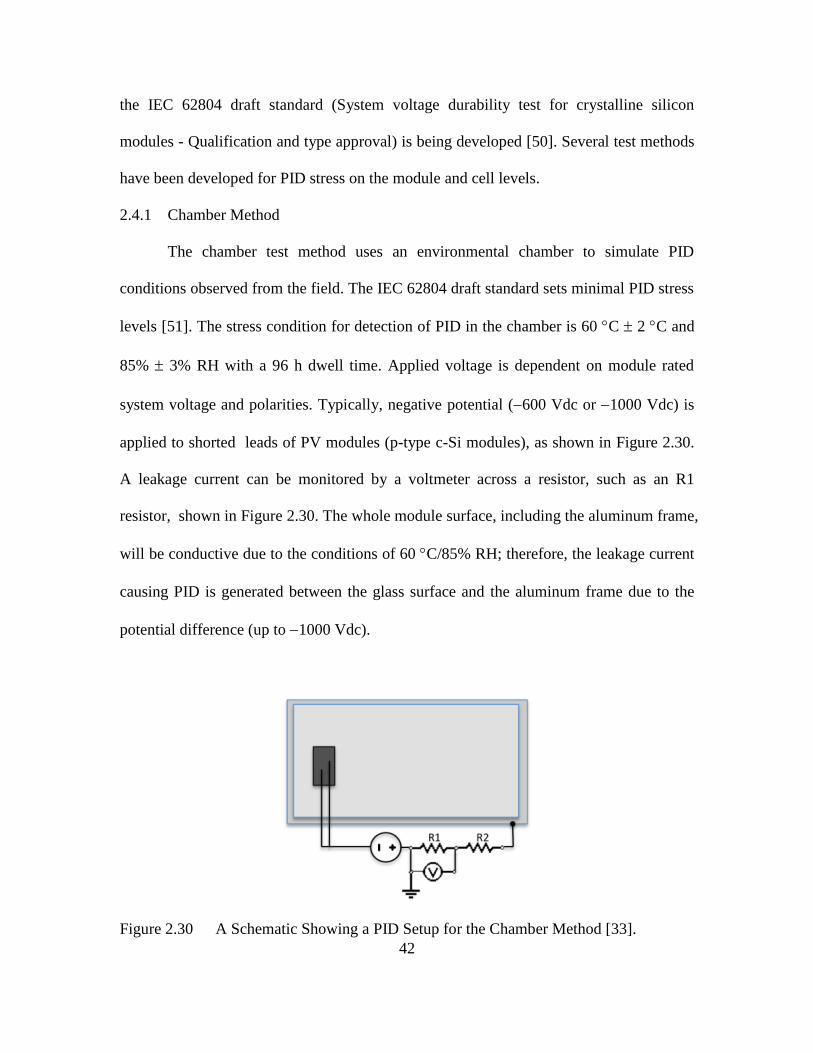
42
the IEC 62804 draft standard (System voltage durability test for crystalline silicon
modules - Qualification and type approval) is being developed [50]. Several test methods
have been developed for PID stress on the module and cell levels.
2.4.1 Chamber Method
The chamber test method uses an environmental chamber to simulate PID
conditions observed from the field. The IEC 62804 draft standard sets minimal PID stress
levels [51]. The stress condition for detection of PID in the chamber is 60 C 2 C and
85% 3% RH with a 96 h dwell time. Applied voltage is dependent on module rated
system voltage and polarities. Typically, negative potential (600 Vdc or 1000 Vdc) is
applied to shorted leads of PV modules (p-type c-Si modules), as shown in Figure 2.30.
A leakage current can be monitored by a voltmeter across a resistor, such as an R1
resistor, shown in Figure 2.30. The whole module surface, including the aluminum frame,
will be conductive due to the conditions of 60 C/85% RH; therefore, the leakage current
causing PID is generated between the glass surface and the aluminum frame due to the
potential difference (up to 1000 Vdc).
Figure 2.30 A Schematic Showing a PID Setup for the Chamber Method [33].

43
2.4.2 Metal Foil Method
Instead of depending on 85% RH, the metal foil method uses a sheet of aluminum
or copper foil as a conductive layer to make a front surface, including the aluminum
frame, conductive [46, 52-55]. This method does not need the environmental chamber
since the metal foil provides uniform contact all over the surface and frame. The test
temperature and time are 25 C and 168 h, respectively. The module rated system voltage
is applied to a test module. This simple PID test method may cost less than the chamber
test method, but it takes longer to detect reasonable PID. Soiling on the PV module glass
may increase PID susceptibility [56], and the metal foil test condition could represent
PID of heavily soiled modules [57]. Therefore, the metal foil method could be used for
soiled-PV module PID testing research.
(a) (b)
Figure 2.31 Schematic Drawing of (a) the Metal Foil Method and (b) a Photograph
[58].
2.4.3 Corona Discharge Method
This is a cell-level PID testing method that does not require module lamination.
Instead of sodium ions (Na+), positive charges are deposited intentionally on the sample

44
surface with high voltage (~ 11 kV) [30, 34]. Therefore, the tested cell showed PID
degradation. This method is quick and convenient in carrying out PID testing. The corona
discharge setup is shown in Figure 2.32.
Figure 2.32 Corona Discharge Method for PID Testing [34].
2.5 PID Solutions
Although the PID mechanism is still unclear, there are various methods for
avoiding PID. PID can be avoided on three different levels: cell level, module level, and
system level.
2.5.1 Cell Level
The most well-known method for avoiding PID is the modification of the SiNx
ARC layer. PID can be suppressed by increasing the RI of the SiNx ARC film [28, 34, 36,
37, 59]. Increasing the RI of SiNx ARC (> 2.1) should be considered carefully because
the cell efficiency will be decreased as the RI increases. Therefore, compromise is needed
to avoid PID as well as efficiency loss in ARC. It also was reported that the deposition
process of the SiNx ARC could make a change in PID susceptibility [28, 60, 61].
However, the detailed information of the different processes for the SiNx deposition has
not been disclosed.

45
Another method to prevent PID is adding a thin oxide layer (SiO2) between the
SiNx layer and the emitter layer of the cell [62-65]. The SiO2 layer could be added during
post implant anneal when the ion implantation process is used to create the emitter. For
common POCl3-diffused solar cells, the thermal oxidation process typical for oxide
growth also is used to grow the SiO2 layer. A UV lamp also could be used to grow the
oxide layer [65]. A suitable thickness for the oxide layer to prevent PID has been found
to be 7–10 nm [63]. Figure 2.33 shows that the SiO2 layer is comparable for the two
different oxidation processes.
Figure 2.33 SEM Image of a Solar Cell Cross Section of (a) an Ion Implanted Cell and
(b) a Modified POCl3 Sample, Which has a Diffusion-Furnace-Grown SiO2 after
Phosphosilicate Glass (PSG) Removal [63].
Recently, it was observed that a well-controlled phosphosilicate glass (PSG) layer
between the SiNx ARC and the emitter protects cells from PID [66]. The SIMS profile of
this PSG-layer cell showed a decrease in sodium where the PSG layer is located, as
shown in Figure 2.34. The specific mechanism that blocks PID in the PSG layer is
unclear. It is speculated that the PSG layer acts as a sodium-gettering layer [67].
(a) (b)

46
Figure 2.34 SIMS Depth Profile of (a) a Standard Solar Cell and (b) the PSG Layer
Added to the Solar Cell [66].
2.5.2 Module Level
Even if PID-susceptible cells are used in building the PV module, PID still could
be prevented by using alternative materials on the module level. It has been observed that
the amount of leakage current is related to PID susceptibility, although it is not always
proportional [28]. Therefore, PID can be suppressed by using high volume resistivity
encapsulant materials (~ 7 1016 -cm) hindering the ionic current flow through the

47
encapsulant instead of using EVA (~ 1 1014 -cm), which is one of most common
encapsulant materials in commercial PV modules. Those encapsulants include ionomer
[68, 69], polyolefin [70], and PID-resistant EVA [71]. As shown in Table 2.3, EVA is
one of the low volume resistivity materials, along with PVB, so these materials are not a
good choice for building a PV module with PID-susceptible cells. Another method to
block the ionic current flow through the cell is adding additional material between the
module glass and the cell. It has been shown that a thin film of polyethylene (~ 30 m
thickness with volume resistivity material of 1.8 1017 -cm) between the glass and
PID-susceptible EVA effectively prevents PID [72]. A Corning Willow glass sheet added
between the PV module glass and the cell also perfectly prevents PID. A detailed
explanation is presented in Chapter 7.
Table 2.3 Electrical and Optical Properties of Different Encapsulant Materials [70]
Encapsulant
material
Volume resistivity
(-cm)
Transmittance
(%)
EVA 1.0 1014 91.0
PVB 4.8 1012 91.0
TPU 2.7 1014 90.0
Silicone 6.0 1015 98.9
Polyolefin 2.0 1016 92.0
Ionomer 7.1 1016 93.4

48
Using alternative PV module glass is another way to avoid PID on the module
level. Soda-lime glass that is PID-susceptible has been used widely as a common PV
module glass. It has been reported that PID was suppressed when quartz or borosilicate
glass was used as a PV module glass [19, 33]. A PV module with an aluminosilicate
chemically strengthened glass instead of soda-lime glass showed strong PID resistance,
although its thickness is only about 0.85 mm [73]. Another candidate is an acrylic-film
material, which is used widely for outdoor structures, such as signboards. It has been
shown that the PV module composed of an acrylic-film coversheet instead of the soda-
lime glass was PID-resistant [74]. TiO2-coated soda-lime glass was reported as a PID-
prevention method. TiO2 film coated with a thickness of about 200 nm inside of PV
module glass showed great PID resistance [75]. Hydrophobic-ARC-coated PV module
glass also showed a reduction of PID [76]. Chemical coating above the PV module glass
is another way to avoid PID [77].
2.5.3 System Level
One interesting characteristic of PID is that the PID degradation is reversible.
PID-affected cells and modules can be recovered by applying reverse potential [28]. The
PV inverter company SMA has been offering a system-level PID solution, which is called
PV Offset Box [78]. The PV Offset Box is an accessory that works with a PV inverter
and enables reverse potential for the PV modules at nighttime for PID recovery.
Therefore, PID modules that are affected during the daytime could be recovered at night.
Using a micro inverter also avoids PID on the system level [36]. Most micro
inverters are rated to match one PV module. Therefore, DC voltage of the entire PV
system using micro inverters is less than 50 Vdc, which is classified as extra-low voltage,

49
while the common PV system using a normal inverter is up to 1000 Vdc. Since the
system voltage using micro inverters is extremely low, there would not be a chance for
PID.
2.6 PID of Other Cell Technologies
As previously mentioned in Section 2.3, PID-s (PID of the shunting type) is only
observed from p-type crystalline silicon solar cells. Since PID became a serious issue for
p-type cells, different technology cell and module manufacturers carried out PID testing
to ensure the reliability of their products. The heterojunction with intrinsic thin-layer
(HIT) solar cells have been known to be PID-resistant regardless of applied bias [79, 80].
The HIT cell is basically an n-type cell that uses transparent conductive oxide (TCO) as
an ARC [81], while common p-type diffused junction solar cells use a SiNx ARC [82]. It
is thought that TCO, which causes no charge accumulation on the cell surface, is a much
more conductive layer than the SiNx ARC, which is an insulating layer that causes charge
accumulation, and makes the HIT cell PID-resistant [83]. Arizona State University (ASU)
Solar Power Laboratory (SPL) also has an ability to fabricate HIT cells in a pilot line.
The SPL single HIT cell coupon was tested for PID and showed PID-resistance
regardless of polarity of applied bias, as shown in Figure 2.36.
Figure 2.35 HIT Cell Structure [84].

50
Figure 2.36 PID Test Results of ASU SPL HIT Cell.
Another common n-type cell is an interdigitated back contact (IBC) solar cell,
such as the SunPower cell. Naumann et al. [85] investigated the PID effect of IBC solar
cells. They observed a degradation of a front side passivation layer from the IBC cell in
contrast to the p-type cell, which shows junction shunting. A loss of the passivation layer
causes an increase of surface recombination, which results in current loss in the cell
operating condition. The mechanism is different from PID-s, so it is called a degradation
of the front side passivation layer (PID-p) [85]. Interestingly, the PID result of their n-
type IBC cell showed the degradation when positive voltage was applied [85]. This result
was the opposite with SunPower’s IBC cell, which was known to be sensitive to the
polarization effect. However, the n-type IBC cell with the front floating emitter showed
the PID-p when negative potential was applied [86], while the n-type IBC cell with the
front surface field [85] experienced the PID-p at positive potential.
0
50
100
150
200
250
300
350
0
0.2
0.4
0.6
0.8
1
0 50 100 150 200
Sh
un
t R
es
ista
nc
e (Ω
)
No
rma
lize
d P
ow
er
Time (h)
Power at STC
Rshunt
−600V +600V

51
The PID-p also was observed from the n-type front junction cells with negative
potential applied [87]. Due to the negative voltage to the n-type front junction cell,
positive charges caused by the leakage current are trapped in the SiNx, as shown in Figure
2.37 (b). The trapped positive charges lead to an increase in the minority carriers
(electrons) in the p-type front layer; therefore, the surface charge recombination increases.
Hara et al. [87] observed that the n-type front junction cell experienced PID-p even when
chemically strengthened glass (CSG) [73], known as an alternative glass material for p-
type modules for preventing PID-s due to its very low sodium concentration, as
mentioned in Section 2.3.2, was used for the module glass. Therefore, it was concluded
that PID-p for an n-type front junction cell is not related to the presence of sodium in
glass.
Figure 2.37 Schematic Diagram Shows the Proposed Mechanism of PID-p in N-Type
Si PV Modules. (a) N-Type IBC Cell Reported in [27]. (b) N-Type Front Junction Cell
[87].
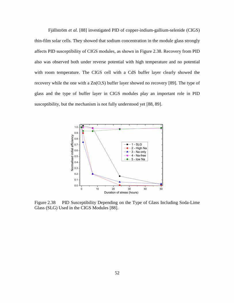
52
Fjällström et al. [88] investigated PID of copper-indium-gallium-selenide (CIGS)
thin-film solar cells. They showed that sodium concentration in the module glass strongly
affects PID susceptibility of CIGS modules, as shown in Figure 2.38. Recovery from PID
also was observed both under reverse potential with high temperature and no potential
with room temperature. The CIGS cell with a CdS buffer layer clearly showed the
recovery while the one with a Zn(O,S) buffer layer showed no recovery [89]. The type of
glass and the type of buffer layer in CIGS modules play an important role in PID
susceptibility, but the mechanism is not fully understood yet [88, 89].
Figure 2.38 PID Susceptibility Depending on the Type of Glass Including Soda-Lime
Glass (SLG) Used in the CIGS Modules [88].

53
Chapter 3
POTENTIAL-INDUCED DEGRADATION AND INCOMPLETE RECOVERY
3.1 Introduction
One of the high-voltage stress (HVS) based performance-loss issues experienced
by photovoltaic (PV) modules in the field is called potential-induced degradation (PID)
[28]. It has been observed that PID-stressed PV modules showed significant output power
decrease (~ 30%), even more at low irradiance level, and increase of hot-spot risk [28, 37,
90]. In response to this field issue, a new IEC standard for PID is being developed [50,
91]. This degradation is mainly due to a cell junction shunting [33, 35, 36, 43], so the PID
is more specifically called PID of the shunting type (PID-s) [35, 43] in order to
discriminate other PID, such as electrochemical corrosion [17]. Sodium has been
suspected to cause PID [33], and source of sodium identified in the PV module glass [19],
which is usually soda-lime glass. It has been shown that sodium decorated stacking faults
located from the cell surface through junction lead to shunting through a thin quasi-
metallic layer [35, 42, 43]. The PID/PID-s has only been observed with p-base crystalline
silicon (c-Si) cells negatively biased to the frame. This issue could technically be
addressed at the cell/module manufacturing level or at the installed system level. At the
manufacturing level, the PID issue can be addressed by modifying the silicon nitride anti-
reflection coating (ARC) [28, 37], by preventing ion conduction through encapsulant or
by eliminating sodium content in the glass superstrate [19, 32]. If the system is already
installed in the field with PID susceptible cells/modules, the PID issue can still be
addressed by applying a reverse potential on the modules during the nighttime [36, 52] so

54
that the cells are positively biased to the frame. Since the energy consumption during this
recovery period is so small when compared with the energy production during the
daytime, the reverse-potential approach to address the PID issue has been implemented
by many system owners. However, recent papers separately discuss an incomplete
recovery under reverse potential in terms of efficiency at high and low irradiance levels,
shunt resistance of cells, and the quantum efficiency (QE) [33, 52, 92]. Moreover, QE
measurement on PID-stressed cells has not been thoroughly investigated yet, although
QE loss at short wavelength was observed and briefly reported in PID-stressed cells by
our research group [92, 93]. QE curves of solar cells are obtained by measuring the cell’s
light-generated current at various wavelengths when monochromatic light shines on the
cell. This measured current is very sensitive to the cell’s shunt resistance, and it may lead
to scaling error when shunt resistance is very low in, for example, PID-stressed cells. In
this chapter, we present a detailed analysis on the effectiveness of the reverse-potential
method on the recovery of the PID-subjected cells and incompleteness of QE recovery,
which have been previously published [92, 93]. This chapter also presents the challenges
in measuring accurate QE of heavily shunted cells and the QE results obtained using a
newly developed ultra-low impedance accessory. Investigation of the source of sodium is
presented in last section of this chapter.
3.2 Experiments
Test coupons (one-cell laminates) were constructed using common commercial-
grade construction materials of glass, EVA, cell, and backsheet. The experiments were
performed using 156 mm × 156 mm size p-base monocrystalline silicon cells, which are
susceptible to the PID issue. The PID stress experiments were carried out at −600 V for

55
88 h at two different temperatures (60 °C and 85 °C) with 0% relative humidity (RH).
The front glass was fully covered with an adhesive conductive aluminum tape to obtain
uniform conductivity throughout the glass surface. The negative voltage was applied to
the shorted leads of test cell-coupon and the positive voltage was applied on the
aluminum tape covering the front glass surface.
Before and after the PID test, all test samples were characterized by light I–V
(LIV), dark I–V (DIV), electroluminescence imaging (EL), infrared imaging (IR), and
quantum efficiency (QE). A steady-state solar simulator was used to take the I–V
measurements. The recovery experiments were carried out using a reverse potential of
+600 V for 88 h at 60 °C, 0% RH. The reverse-potential-subjected samples were
characterized using the techniques identified above and then stored at room temperature
without any imposed potential and periodically characterized to observe additional
recovery, if any. Also, some of the PID-stressed samples that were not subjected to
reverse-potential recovery were stored and periodically characterized at room
temperature to compare the recovery rates between the reverse-potential samples and
room temperature stored samples. The recovery rate and extent are reported in terms of:
power recovery at both high and low irradiances; shunt resistance recovery, and
quantum-efficiency recovery at wavelengths between 350 and 1100 nm.
The QE measurement artifacts of heavily shunted cells can be simulated using an
externally connected parallel resistors (Rp), as shown in Figure 3.1. If the QE system
input impedance is not exactly zero, a small voltage drop will develop at the QE system
connection, driving current through the external Rp instead of to the QE system to be
measured. Thus, the measured QE decreases. This wavelength-independent scaling error

56
in QE can be significantly reduced by utilizing a very-low impedance method. A new
ultra-low impedance accessory developed by PV Measurements, Inc. has been utilized in
the QE system of this work to minimize the QE drops of the heavily shunted cells.
Figure 3.1 Basic Circuit Diagram of a Solar Cell Indicating Shunt (Rsh or Rp) and
Input Impedance of QE System
3.3 Incomplete Recovery of Power and Shunt Resistance
Figure 3.2 (a) shows the progress of PID and recovery of maximum power (Pmax)
at 1000 W/m2 and on shunt resistance. After 88 h of PID stress at 60 °C, the remaining
power was determined to be 70% when compared with the initial power, and the shunt
resistance dropped to under 1 . After the PID test, the sample was stored at room
temperature with no potential for more than 75 days, and the power at 1000 W/m2 is
determined to be recovered to about 92%. However, the recovery of shunt resistance is
still very low although most of the power at this high irradiance level is recovered.
At 85 °C PID stress, a much higher power drop in a shorter time of test was
observed, as shown in Figure 3.2 (b). After leaving at room temperature for more than
500 h, the recovered power was only 87% at 1000 W/m2 irradiance level and 60% at 240
W/m2 irradiance level, and the recovered shunt resistance is practically insignificant.

57
Also, it takes much longer time for both Pmax and shunt resistance to be recovered when
compared with the 60 °C-PID-stressed samples due to extensive damage to the cell
materials and/or junction, which may not be a realistic observation in the field.
Figure 3.2 (a) Recovery Rate and Level of Output Power at High (1000 W/m2)
Irradiance Level, and Shunt Resistance during the Recovery Period at Room Temperature
(No Aluminum and No Bias for 1992 h) on a Test Sample Subjected to the PID Stress at
60 °C/0% RH (Aluminum Covered, −600 V, 88 h). (b) Recovery Rate and Level of
Output Power at High (1000 W/m2) and Low (240 W/m2) Irradiance Levels, and of Shunt
Resistance during the Recovery Period at Room Temperature (No Aluminum and No
Bias for 576 h) on a Test Sample Subjected to the PID Stress at 85 °C/0% RH
(Aluminum Covered, −600 V, 44 h).
To observe if an applied reverse voltage at a higher temperature than the room
temperature could recover the cells to a higher level, another set of test coupons were
prepared and subjected to the tests, as shown in Figure 3.3. There is practically no
difference in recovery of power at 1000 W/m2 irradiance level, between 0 V and +600 V
potential, but the reverse potential at high temperature accelerates recovery from PID in a
shorter amount of time compared to room temperature storage with no voltage

58
application as described in [52]. Even though the recovery of power at high irradiance of
1000 W/m2 is as high as 93% of its original, the recovery of the shunt resistance is still
only about 40% of its original. Neither of those cells showed higher than 50% shunt-
resistance recovery after 125-days of room temperature storage. And, recovery speed for
both power and shunt resistance is extremely slow after 40-day storage. This poor
recovery of shunt resistance would have a serious impact on the cell efficiency at low
irradiance levels [90].
Figure 3.3 Normalized Power and Shunt Resistance. Both Coupons Have the Same
PID Conditions (60 °C, −600 V, 88 h) but Different Recovery Methods. Coupon A: 15-
Day Room Temperature Storage with No Bias, Coupon B: +600 V @ 60 °C, 88 h.
This inadequate shunt resistance recovery could cause: (i) a safety issue if the
cells in a module were to operate under shaded/reverse-bias condition with failed bypass
diodes; (ii) very-low energy production at the sites where the module performance

59
primarily depends on the prevailing low-light conditions. All the fresh test coupons
showed practically 0 A current flowing through the cell at −12 V. Due to cell shunting
after the PID stress, the observed reverse current at −9 V was higher than 8 A just after
the stress test and even after a 24-day recovery period at room temperature. Because of
this localized high current in reverse bias, as shown in Figure 3.4 (b) and (c), the cell was
found to be damaged due to high localized temperature, as shown in Figure 3.4 (d). The
light emission (white spots) shown in the reverse bias EL image (Figure 3.4 (b), is
attributed to different type of shunts (ohmic or non-ohmic), in this case shunts are caused
by PID, and source of shunt can be identified by spatially resolved EL imaging with lock-
in thermography (LIT) under reverse and forward bias [94]. It has been reported that light
emission in EL under reverse bias is also related to electrical breakdown [95].
Interestingly, it was observed that this cell was not permanently damaged, i.e.,
breakdown. The damaged cell was stored at room temperature for 32 days and then I–V
and EL were carried out. The results, as shown in Figure 3.4 (e), show that there was
increase of Pmax and shunt resistance when compared with the day that cell was damaged
due to reverse-bias EL measurement. EL images (not shown here) also showed brighter
damaged area than before. The cell has been monitored more than 200 days to see if there
is complete recovery from PID; however, no complete recovery has been obtained. This
result supports that the remaining sodium atoms in the stacking faults or the remaining
sodium ions in other regions, such as SiNx or SiOx of the cell [48] still have a critical
impact on PID-stressed cells. It is assumed that those remaining sodium atoms hinder the
100% recovery of shunt resistance and cause a very-high possibility that PID-stressed
cells could be easily damaged under reverse-bias condition.
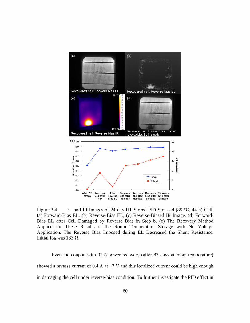
60
Figure 3.4 EL and IR Images of 24-day RT Stored PID-Stressed (85 °C, 44 h) Cell.
(a) Forward-Bias EL, (b) Reverse-Bias EL, (c) Reverse-Biased IR Image, (d) Forward-
Bias EL after Cell Damaged by Reverse Bias in Step b. (e) The Recovery Method
Applied for These Results is the Room Temperature Storage with No Voltage
Application. The Reverse Bias Imposed during EL Decreased the Shunt Resistance.
Initial Rsh was 183 Ω.
Even the coupon with 92% power recovery (after 83 days at room temperature)
showed a reverse current of 0.4 A at −7 V and this localized current could be high enough
in damaging the cell under reverse-bias condition. To further investigate the PID effect in

61
terms of light I–V in negative voltage, another coupon was built and PID stressed at
60 °C/−600 V/88 h. Figure 3.5 shows I–V curves of the coupon at 240 W/m2 irradiance
level, which is a worse-performance condition for a shunted cell. There was a large
reverse current after 88 h PID while a fresh cell had no reverse current at all, as shown in
Figure 3.5. The 98-h PID recovery of the cell (94% Pmax at 1000 W/m2 and 75% Pmax at
low irradiance, respectively) still showed high reverse current due to very slow recovery
of Rsh. Therefore, it is suggested that Rsh should be monitored with Pmax in evaluating PID
recovery. Additionally, it was observed that the increase in reverse current is nonlinear,
which represents that shunting caused by PID is not a simple shunting. The presence of
localized shunts even after extensive recovery with or without reverse potential indicates
the presence of traces of sodium at the junction.
Figure 3.5 I–V Characteristics of PID-Stressed and Recovered Cell at Low Irradiance
(240 W/m2) (PID 60 °C/−600 V/88 h; PID Recovery at Room Temperature/No Bias/98 h).

62
3.4 Scaling Error of Heavily Shunted Cells
The QE measurement becomes very sensitive in the heavily shunted cells. If the
series resistance of the test cell along with the input impedance of the QE system is
substantial, then a significant voltage develops at the point of current generation. That
voltage then drives current through the shunt in the cell, allowing less current to exit the
solar cell and enter the QE system. This voltage significantly diminishes the measured
QE, especially in the heavily shunted cells. The measured QE of the shunted cells will
only shift up or down (scaling error) with no wavelength-dependent error. Figure 3.6 (a)
shows QE curves, obtained at various PID recovery stages, of the same test coupon used
in Figure 3.2 (b). It was initially thought that the large QE drop shown in Figure 3.6 (a)
was due purely to the PID effect of the test device with no influence from the measuring
equipment. When the integrated short circuit current (Isc) from the QE curve was
compared with the measured Isc from the I–V curve, it was realized that there is a
significant influence of test equipment on the accuracy of the QE curve. The decrease of
Isc based on the integration of the QE curve after PID is about 55%, which is a great
difference than the Isc from the conventional white light I–V measurement (7%).

63
Figure 3.6 (a) QE Curves of Same Test Coupon as Shown in Figure 3.3, (b) QE
Curves of a Fresh Cell Coupon Connected with Various Parallel Resistors (Rp).
Since there were experimental complications in controlling the shunt resistance
with high level of repeatability, a physical resistor was used to perform the simulated-PID

64
experiments. To simulate a PID shunted cell, an external resistor was connected in
parallel across the two leads of a fresh coupon that was not subjected to any PID stress.
As shown in Figure 3.6 (b), QE with various parallel resistances (Rp) followed the same
trends as that of the PID-affected cell. This result supports that the QE drop in a PID-
affected cell is not due purely to the PID effect but also partly to the measuring
equipment impedance.
To measure the QE of heavily shunted cell accurately, QE curves of the cell could
be normalized and the scaling problem could be alleviated by matching its integrated Isc
with the white light Isc of I–V measurements. Another way to address this scaling
problem is to make the input impedance of the QE equipment as small as possible.
Therefore, an accessory having very-low input impedance, developed by PV
Measurements, Inc. was connected to the existing QE system. Figure 3.7 shows the
measured QE curves obtained without and with low impedance accessory; this figure also
includes the QE curves obtained with three 1- resistors incrementally connected in
parallel. Encouragingly, the QE curves (with parallel resistors) with the low impedance
accessory have dramatic improvements (Figure 3.7 (b)) when compared with the ones
without it (Figure 3.7 (a)). Therefore, it is highly recommended that QE measurements on
PID-affected cell use a QE system with low input impedance. Input impedance of QE
system without the very-low input impedance accessory was measured at 0.35 while
the one with very-low input impedance accessory is about 0.015 . Measuring a severely
shunted cell, (e.g. Rsh = 1 Ω), needs an input impedance smaller than 0.015 in order to
minimize scaling error. The use of low impedance accessory is determined to be a must
for the nonintrusive QE measurements of heavily shunted PID cells connected in series in
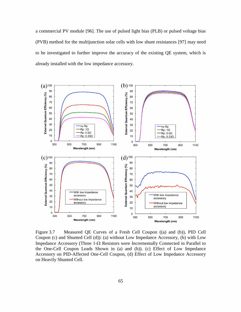
65
a commercial PV module [96]. The use of pulsed light bias (PLB) or pulsed voltage bias
(PVB) method for the multijunction solar cells with low shunt resistances [97] may need
to be investigated to further improve the accuracy of the existing QE system, which is
already installed with the low impedance accessory.
Figure 3.7 Measured QE Curves of a Fresh Cell Coupon ((a) and (b)), PID Cell
Coupon (c) and Shunted Cell (d)): (a) without Low Impedance Accessory, (b) with Low
Impedance Accessory (Three 1- Resistors were Incrementally Connected in Parallel to
the One-Cell Coupon Leads Shown in (a) and (b)). (c) Effect of Low Impedance
Accessory on PID-Affected One-Cell Coupon, (d) Effect of Low Impedance Accessory
on Heavily Shunted Cell.

66
3.5 Incomplete Recovery of Quantum Efficiency
Figure 3.8 (a) shows QE curves of coupon B, identified in Figure 3.3, after PID
(Pmax: 81%) and reverse-potential recovery (Pmax: 96%) steps. The QE of after-88 h-
recovery stressed/shunted sample was found to be much lower than the initial due to a
reason mentioned in Section 3.4. To observe if the relative QE curves between the
fresh/initial and recovered cell are identical, these curves were normalized. As shown in
Figure 3.8 (a), the QE values for the photons between 350 and 600 nm wavelength are
found to be lower than the QE of fresh/initial cell. This phenomenon was clearer in 85 °C
PID-stressed cell, as shown in Figure 3.8 (b). None of the QE curves in recovery process
were identical to initial ones at wavelength range from 350 to 600 nm. QE drop at short
wavelength range shows that there is another PID effect in addition to junction shunting
since QE measurement of shunt-only cell affects the overall QE scale down as mentioned
in Section 3.4. It is well known that change of QE at short wavelength range is caused by
changes in front surface recombination velocity or emitter diffusion length [98]. Further
details are described in Chapter 4. It was shown that a huge increase in the front surface
recombination velocity is necessary in aligning the PID mechanism to the inversion
model [99]. In addition, a degradation of front surface passivation that leads to an
increase in surface recombination was observed in interdigitated back contact (IBC) solar
cells after PID stressing [85]. Therefore, PID stressed cells might possibly have a high
front surface recombination velocity. The mechanism for front surface recombination
velocity increase after PID is not fully understood and it will be a subject of future
research.

67
Figure 3.8 (a) QE of Coupon Used in Figure 3.3, QE of Fresh/Initial, PID-Stressed
and Recovered Cells (PID Stress at 60 °C/−600 V/88 h; PID Recovery at 60 °C/+600
V/88 h), (b) Normalized QE of Figure 3.6 (a), QE of Fresh/Initial, PID-Stressed and
Recovered Cells (PID Stress at 85 °C/−600 V/44 h; PID Recovery at RT/No Bias/408 h).

68
3.6 Effect of Sodium Concentration in Glass on PID
The transport of sodium from the module glass to a cell surface is strongly
suspected to cause PID. Using an alternative glass with no sodium content, such as quartz,
effectively protects cells in a module from PID [19, 73]. However, it is not clear that a
particular amount of sodium is critical for PID. In order to further investigate the effect of
sodium content in the glass on PID, two one-cell coupons using different type of glass
were prepared and stressed in a condition described in Section 3.2. The only difference is
that 60 °C/85% RH was applied to the test conditions instead of using front aluminum
covered tape. The encapsulated cells were standard commercial cells known to be
susceptible to PID. Coupon 1 used soda-lime glass as is typical in commercial PV
modules. Coupon 2 used borosilicate glass, which has a lower sodium content than soda-
lime glass and has also been shown to prevent electrochemical corrosion in thin film
modules [25]. Measurement with energy dispersive spectroscopy (EDS) showed that
primary impurity in soda-lime glass is sodium with 16% by weight. As expected,
borosilicate glass has a much lower sodium content at 6.5% by weight. PID was observed
in both of one-cell coupons and confirmed by I–V and EL. Figure 3.9. shows that the
borosilicate coupon is much more resistant against PID even at 100 h PID stress while the
soda-lime glass coupon was completely shunted after 24 h PID stress. These results
support that sodium in a glass plays an important role in causing PID. The borosilicate
glass could be used in PV modules to minimize PID, but it cannot completely protect
cells from PID and the cost would be significantly higher.

69
Figure 3.9 PID (60 °C/85% RH, −600 V) Progress of Soda-Lime Glass Coupon and
Borosilicate Glass Coupon
3.7 Summary
The PID-recovery methods presented in this chapter show very good regeneration
(up to 96%) of Pmax at a high irradiance level of 1000 W/m2. However, the recovery of
shunt resistance and efficiency at low irradiance levels is extremely low when compared
with the recovery of Pmax/efficiency at a high irradiance level. The poor cell efficiency at
low irradiance levels would lead to lower energy production at predominantly low
irradiance level locations and durations. The near-full Pmax recovered cells still show
much higher reverse-bias current when compared with the fresh cells. Therefore, any
recovered cells/modules through the application of reverse potential and/or high
temperature may pose safety risks under shaded condition if the protecting bypass diodes
happen to fail in the field. Consequently, the Pmax recovery at high irradiance level alone
should not be considered as the sole parameter indicating the full recovery from the PID
issue as the cells still retain some of the defects caused by the PID damage.
The two modern, commercial QE systems utilized in this work had substantial
scaling error when measuring heavily shunted cells, such as PID-affected cells. The
existing QE system with the low impedance accessory effectively minimizes (though not

70
totally eliminates) QE scaling error issues in the shunted cells. Consequently, it is highly
recommended to use the QE systems built with the low impedance accessory, not only
for the PID-related reliability research but also for the solar cell design research.
Two different glass types (soda-lime and borosilicate glass) were utilized to
determine PID effects. It was shown that borosilicate glass has a lower sodium content
(6.5%) than soda-lime glass (16%) by EDS analysis and that a borosilicate glass coupon
is more PID resistant than using soda-lime glass. It is concluded that sodium in glass is
critical in PID effect.

71
Chapter 4
QUANTUM EFFICIENCY LOSS CAUSED BY PID
4.1 Introduction
There are several studies indicating that the PID loss is caused by the migration of
sodium ions from glass superstrate to the cell [19, 31, 43]. One of the primary solutions
to address PID issue is a modification of chemical and physical properties of
antireflection coating (ARC) on the cell surface [28, 37]. Depending on the edge isolation
method used during cell processing, the ARC layer near the edges may be uniformly or
non-uniformly damaged. Therefore, the pathway for sodium migration to the cell junction
could be either through the cell surface if surface and edge ARC have low quality or
through the cell edge if surface ARC is high quality but edge ARC is damaged [28]. In a
previous study [92], a wavelength dependent QE (quantum efficiency) loss and recovery
after PID stress testing was shown. In this study, two PID susceptible cells from two
different manufacturers have been investigated. The QE measurements of these cells
before and after PID stress were performed at both surface and edge locations to
determine the influence of sodium migration pathway on the wavelength dependent QE
loss. PID-affected QE curves based on QE loss at short wavelength presented in the
previous chapter have also been modeled in this chapter. Investigation of the challenges
with an alternate PID inversion model [40] is presented in this chapter. To rapidly screen
a large number of cells for PID stress testing, a new but simple test setup that does not
require laminated cell coupon has been developed and is used in this investigation.

72
4.2 Experiments
The solar cells used in this study were standard 156 × 156 mm p-base
monocrystalline silicon cells with known susceptibility to PID. Two different
manufacturers’ cells (M1 and M2) were used in this investigation. Two test setups were
used to perform PID stress testing. In the first setup, laminated one-cell coupons were
used. In order to fabricate laminated one-cell coupons, each cell was encapsulated as in a
standard PV module construction (glass – EVA – cell – EVA – backsheet) using a
commercial PV module laminator. Typical tempered solar glass (soda-lime glass), EVA,
and TPE backsheets were used in fabricating the laminated one-cell coupons. The PID
stress conditions for the coupons were obtained using a weathering chamber at 60 °C/0%
relative humidity (RH) or 85 °C/0% RH. Instead of maintaining commonly used 85% RH
for the glass surface conductivity during PID test, an aluminum tape with conductive
adhesive was used to cover the front glass surface of the coupons. The voltage of −600V
was applied on the cell with respect to aluminum tape on a coupon glass. More detailed
description of the setup is presented elsewhere [92].
In the second setup, simple physically stacked (no lamination) construction
materials were used [31, 43, 100]. The laminated coupon based PID test setup is good to
observe if a cell is PID susceptible or not; however, in this method several physical and
surface analyses of the cell (before and after PID stress testing) using various
characterization techniques would be limited due to difficulty in delaminating cell from
other coupon materials especially encapsulant. Therefore, a simple and rapid PID test
setup that does not require laminated coupons has been developed at Arizona State
University. Same materials used for the laminated coupon method were utilized in this

73
new setup as well. The glass, EVA, and cell are stacked, as shown in Figure 4.1 left, and
600V was applied to the bottom plate. Using this new setup, the cells were PID stressed
at 60 °C/0% RH in a conventional laboratory convection oven. By using this new method,
we were able to secure, after the PID stress testing, the entire bare cell with no breakage
or EVA residue on it.
Figure 4.1 Photo of Setup #2
All the laminated one-cell coupons and bare cells were characterized by light I–V,
dark I–V, electroluminescence (EL) imaging, dark lock-in thermography (DLIT), and QE
before and after PID tests. All QE values obtained after PID tests were normalized due to
the scaling error [93]. QE measurements at multiple cell locations of interest were carried

74
out to investigate the wavelength dependent QE loss. Based on the lessons learned in the
previous study [92], primary attention was paid to the QE loss observed at the short
wavelength range (300 – 700nm). After PID stress and initial characterizations, all the
degraded coupons and bare cells were stored at room temperature and monitored the
recovery process as was done in the previous study [92].
4.3 Quantum Efficiency Loss Modeling
The unrecovered QE or QE loss could be attributed to change of front surface
recombination velocity (FSRV) or emitter diffusion length [98, 101]. PC1D was used in
simulating this effect, and QE loss shape of PID-stressed coupon in short wavelength was
clearly demonstrated by either increasing FSRV or decreasing emitter diffusion length
(not shown here). However, in a real PID cell, measuring area includes both PID-affected
area and no/less PID-affected area due to a bigger beam size (1 mm × 5 mm) of
monochromatic light in QE system than shunting spots in PID-affected area. It has been
observed that PID-stressed cell has localized shunting spots, which appear circular-
shaped with a diameter of 5-20 μm [35]. Since PC1D simulates the homogeneous region
only, it was considered that parallel connection of no/less PID-affected area assuming
low FSRV and PID-affected area assuming high FSRV were considered as a measured
area. Each area of QE is obtained by using the following equations [102], and parameters
used in creating these two areas are shown in Table 4.1. To make the parallel connection
of those two different areas, total QE (non-PID area + PID area) plot was calculated by
multiplying a factor (for example, PID area: 0.7 and non-PID area: 0.3 were used).

75
QEE =aLp
a 2Lp2 -1
´
SpLp
Dp+aLp - e
-ax jSpLp
Dpcosh
x j
Lp+ sinh
x j
Lp
æ
èçç
ö
ø÷÷
SpLp
Dpsinh
x j
Lp+ cosh
x j
Lp
-aLp - e-ax j
é
ë
êêêêê
ù
û
úúúúú (3.1)
QEB = e-ax j aLn
a 2Ln2 -1
´ aLn -
SnLnDn
coshH
Ln- e-aH
æ
èç
ö
ø÷+ sinh
H
Ln+aLne
-aH
SnLnDn
sinhH
Ln+ cosh
H
Ln
é
ë
êêêê
ù
û
úúúú
(3.2)
QE = QEE +QEB (3.3)
where
QEE: QE at emitter region
QEB: QE at base region
Lp: emitter diffusion length (μm)
Sp: front surface recombination velocity (cm/s)
Dp: emitter diffusivity (cm2/s)
xj: emitter thickness (junction depth) (μm)
α: absorption coefficient (cm-1)
Ln: base diffusion length (μm)
Sn: back surface recombination velocity (cm/s)
Dn: base diffusivity (cm2/s)
H: base thickness (μm)
76
Table 4.1 Parameters for QE Plots
QE Parameters
for
non-PID-affected area
QE Parameters
for
PID-affected area
Sp (cm/s) 1 × 10⁴ 5 × 10⁴
Lp (μm) 1 1
Dp (cm2/s) 4 4
xj (μm) 0.5 0.5
Sn (cm/s) 1 × 10⁴ 1 × 10⁴
Ln (μm) 200 200
Dn (cm2/s) 27 27
H (μm) 200 200
Figure 4.2 shows simulated QE results from the calculation mentioned above.
Blue curve can be represented as QE of non-PID-affected homogeneous area. Calculated
QE of PID-affected homogeneous area is shown as red curve, and it should be noticed
that QE in short wavelength (300-700 nm) is decreased, as if QE of PID-stressed coupon
shown in Figure 3.8 is plotted. QE of total area close to real measurement also shows
such QE loss shape in the short wavelength. These results indicate that a cell property
could be changed by defects caused by PID in addition to change of I–V parameters.
Based on the results presented in Section 3.5, these defects leading to decrease QE in
short wavelength may not be removed, although I–V parameters are getting slowly
recovered. As shown in Figure 4.2, the modeled QE at 300-360 nm is clearer in
discriminating QE shifting as FSRV changes. However, QE loss from one-cell coupon, as
shown in Figure 3.8, has no values at such range due to cut-off wavelength (360 nm) of

77
EVA. Therefore, it is recommended to measure QE of PID-affected area without EVA
and glass to verify this QE model.
Figure 4.2 Calculated QE to Simulate PID-Affected Cell. Blue Curve is based on
Homogeneous Non-PID-Affected Area, Red Curve is based on Homogeneous PID-
Affected Area, and Green Curve is based on a Combination of 70% PID-Affected Area
and 30% Non-PID-Affected Area.
4.4 Detailed Modeling of Surface Charge with Sentaurus
The previous section discussed the effect of changing surface recombination on
QE. It has also been postulated that the sodium ions cause shunting though surface charge.
According to proposed mechanism [40] the large potential difference between the cell
and the frame causes a large amount of sodium to move from the glass, through the EVA
encapsulant and accumulate at the surface of the solar cell. The huge amount of
positively charged sodium ions at the cell surface attract the same amount of negative
charges within the silicon to invert the emitter and eventually shunt the cell [39, 40]. The

78
researchers estimated the amount of surface charges required to show the emitter
inversion for typical n+ emitter with a sheet resistance of ~ 60 Ω/sq is −1 × 1015 cm−2, but
this amount of charges was not able to be applied in PC1D [40]. In this study, a different
semiconductor simulation program, Sentaurus allowing for much higher surface charge to
investigate the proposed mechanism, was applied. In the modelling, typical industrial
solar cell parameters were used, with a p-type base doping of 1 × 1016 cm−3, a peak n-
type emitter doping of 1.5 × 1020 cm−3 and a junction depth of 0.5 µm. Figure 4.3 shows
the band diagram when surface charge of −1 × 1015 cm−2 was applied on an emitter
surface. There was no complete emitter inversion that was shown in [40]. The beginning
of emitter surface started to invert, however the inversion does not extend down to the
junction region as would be required for the inversion to cause the cell to shunt.
Increasing the charge further produced a similar effect to that shown in Figure 4.3. The
surface inverts and would change the surface recombination velocity but the effect
extends less than 10 nm into the emitter and is nowhere near the junction at 0.5 µm. Even
with an unrealistically high level of −1 × 1030 cm−2 charge applied on the emitter surface
the cell does not exhibit shunting. The Sentaurus simulation confirms the results from
Saint-Cast et al., who reported, by comparison of experimental and simulated dark I–V
curves, that the inversion model cannot explain the PID shunting mechanism [99].
Therefore, a recently proposed model based on sodium decorated stacking faults [35] is
preferred to the inversion model to explain the PID mechanism.

79
Figure 4.3 Sentaurus Band Diagram for a Solar Cell, (a): No Surface Charge, (b):
with Negative Surface Charge (−1 × 1015 cm−2)
4.5 QE Loss Observed on Laminated Coupons (Setup #1)
As shown in Figure 4.4 (a), the maximum power (Pmax) and shunt resistance (Rsh)
values were found to be dramatically decreased after PID stress at 85 °C/−600 V/44 h.
Pmax was recovered to approximately 90% of initial while Rsh was recovered at an
extremely slow rate. A significant QE loss was observed, at different locations on the cell

80
surfaces including the cell edges, at the wavelength range between 360 and 700 nm. It is
important to note that the QE loss seen at this low wavelength range was never recovered
while Pmax and Rsh were slowly and partially recovered with respect to time. A separate
mechanism might therefore be responsible for the blue response loss. In order to
determine if the QE loss in the low wavelength region is caused by the reflection
alterations (reflection or absorption) in the ARC layer, the UV-Vis-NIR reflectance
spectra were obtained on a different coupon stressed at 60 °C/−600 V/88 h. Negligible
reflectance spectral difference was observed between pre- and post-PID stress test, as
shown in Figure 4.5. The QE loss in the short wavelength range could be attributed to
increasing front surface recombination velocity (FSRV) or decreasing emitter diffusion
length [101], and it was modelled in Section 4.3.

81
(a)
(b)
Figure 4.4 I–V Parameters (a) and QE (b) Results of a Laminated One-Cell (M1;
Setup 1) Coupon at Various Stages of Investigation: PID 44 h at 85 °C/0% RH, −600 V,
Recovery at Room Temperature (RT).
0
50
100
150
0.0
0.2
0.4
0.6
0.8
1.0
-100 0 100 200 300 400 500 600
Re
sis
tan
ce
(Ω
)
No
mali
ze
d P
ma
x
Time (h)
Pmax
Rsh
Room temperature recovery PID stress
0
10
20
30
40
50
60
70
80
90
100
300 400 500 600 700 800 900 1000 1100
Ex
tern
al Q
ua
ntu
m E
ffic
ien
cy
(%
)
Wavelength (nm)
Initial
PID 22h (Normalized)
PID 44h (Normalized)
Recovery RT 24h (Normalized)
Recovery RT 48h (Normalized)
Recovery RT 72h (Normalized)
Recovery RT 144h (Normalized)
Recovery RT 240h (Normalized)
Recovery RT 408h (Normalized)

82
Figure 4.5 Reflectance of a Laminated One-Cell (M1; setup 1) Coupon at Various
Stages of Investigation: PID 88 h at 60 °C/0% RH, −600 V, Recovery at Room
Temperature (RT). Zoomed-In Plot of Reflectance is shown in a Small Square in Figure
4.5.
4.6 QE Loss Observed on Bare Cells (Setup #2)
In the FSRV model, the QE change at 300 nm is expected to be more sensitive as
compared to the higher wavelength region as presented in Section 4.3. Therefore, if we
observe a higher loss at about 300 nm in the PID-affected cell, it would give us additional
confidence if the FSRV or decreasing emitter diffusion length model is operating after
PID stressing. Measuring QE at 300 nm on the laminated one-cell coupon was not
possible due to UV cut-off wavelength (360 nm) of EVA. Therefore, a new PID test
setup (setup #2) without lamination that would allow QE characterization up to 300 nm
after PID was needed.
Figure 4.6 shows QE results of a PID stressed cell (M1) obtained using the new
method. It is clear that QE loss at 300nm in largest, and this experimental result is
consistent with the one of QE model, as shown in Figure 4.2. Higher QE loss at about

83
300 nm appears to indicate that the FSRV mechanism is probably responsible for the PID
losses.
Figure 4.6 QE of Bare Cell (M1; setup 2) before and after PID 80 °C/24 h/600 V.
QE of PID Affected Area Characterized by EL was carried out. QE of PID Stressed Cell
is normalized.
As shown in Figure 4.7, PID was observed almost exclusively at the edges only
for M2 cells irrespective of laminated coupon method (setup 1) or bare cell method (setup
2) is used. PID was observed all over the surface of M1 cells but, on M2 cells, it was
observed essentially at cell edges only as shown in the exploded EL images of Figure 4.8
(a). It is believed that M2 cells have appropriate ARC layers to prevent PID but
presumably get damaged at the edges during edge isolation process which is commonly
done after diffusion in cell processing lines or the cell had an inadequate edge isolation
process [28]. QE measurements, before and after PID stress, was carried out on areas
where PID was observed (Area 1) and also on areas where no PID was observed (Area 2)
0
10
20
30
40
50
60
70
80
90
100
300 400 500 600 700 800 900 1000 1100
Exte
rna
l Q
ua
ntu
m E
ffic
ien
cy
(%
)
Wavelength (nm)
Initial
PID
PID (Normalized)

84
based on the EL images. Neither area had wavelength dependent QE loss after
normalization (as opposed to M1 cells), as shown in Figure 4.8 (b). These results from
M2 cell appear to indicate that there is another pathway operating for sodium ions to
reach the cell junction without going through ARC layers. If the edge isolation process is
inadequate or inappropriately damaged, junction near the edges is susceptible to PID loss
but the loss would be wavelength independent as the photons do not go through ARC
layer and the FSRV mechanism is not operating.

85
Figure 4.7 Comparison PID Test between (a) Laminated Coupon Method (Setup 1)
vs. (b) Bare Cell Method (Setup 2). M2 Cells were used in Both Methods.
(a) (b)

86
(a)
(b)
Figure 4.8 EL Image before/after PID and QE in 2 Areas. M2 Cell was used.
4.7 Summary
QE loss in short wavelength was simulated by increasing FSRV, and it showed a
similar QE shape as the QE of actual PID-stressed coupons. Result of bare cell QE
measurements enabling QE at around 300 nm clearly matches with the calculated QE loss
model. Depending on edge isolation adequacy or damages of ARC during edge isolation
at the edges, cells may experience PID near edges even if the front surface is well
0
10
20
30
40
50
60
70
80
90
100
300 500 700 900 1100
Ex
tern
al
Qu
an
tum
Eff
icie
ncy
(%
)
Wavelength (nm)
Area 1
Initial
PID
PID (Normalized)
0
10
20
30
40
50
60
70
80
90
100
300 500 700 900 1100
Ex
tern
al
Qu
an
tum
Eff
icie
ncy
(%
)
Wavelength (nm)
Area 2
Initial
PID
PID (Normalized)

87
protected against PID by appropriately modifying the ARC layers. A simple and rapid
PID test method is used, which allowed us to carry out the PID experiments with no
requirement of laminated cell coupon.

88
Chapter 5
EFFECT OF SINX REFRACTIVE INDEX AND EMITTER SHEET RESISTANCE ON
POTENTIAL-INDUCED DEGRADATION
5.1 Introduction
Potential-induced degradation (PID) has become a hot issue in the photovoltaic
(PV) reliability industry due to the likelihood of rapid power degradation. The term PID
was first used by Solon in 2005 [28]. Since its main failure mechanism manifests itself in
cell shunting, the PID is specifically referred to as PID of the shunting type (PID-s) [35,
43]. PID-s is only observed on p-type diffused junction solar cells when the cells are
operated as a PV system which is accompanied by high voltage with severe
environmental conditions, such as high temperature and humidity. Several studies
indicate that PID-s is caused by the migration of sodium ions, and the source of sodium
could be from the PV module glass (typically, soda-lime glass) [19, 33, 44, 103] or
contaminants at the cell surface [104]. A more recent study showed that a root cause of
PID-s is the presence of a sodium-decorated stacking fault penetrating the n-p junction
[35]. The sodium-decorated stacking faults cause junction shunting, and this leads to an
increase of the depletion region recombination current (J02) and the ideality factor (n2)
[43]. It also has been reported that sodium outdiffusion from the stacking fault is
observed as the PID-affected cell is recovered by exposure to high temperature [48].
There are multiple factors that contribute to PID susceptibility in a cell process.
What we would like to clarify among them are the roles of the refractive index (RI) of the
silicon nitride (SiNx) antireflection coating (ARC) and the emitter sheet resistance. Many

89
publications have shown that PID is suppressed by increasing the RI to a value greater
than 2.1 [28, 36, 37]. Pingel et al., showed the general trend of increasing PID-
susceptibility with respect to increasing emitter sheet resistance [28]. In this study, we
verified the effect of SiNx RI and emitter sheet resistance on PID-s.
5.2 Experiments
Industrial standard (156 mm × 156 mm) p-type diffused junction monocrystalline
silicon solar cells were fabricated in the Solar Power Laboratory (SPL) pilot line located
at Arizona State University. The SPL standard p-type cell process flow is shown
schematically in Figure 5.1. For this study, three different SiNx ARC films were
deposited onto wafers by adjusting the SiH4 and NH3 gas flow rates in the plasma
enhanced chemical vapor deposition (PECVD) equipment. All of the ARC film
thicknesses are around 78 nm. The cells were processed identically except for the change
in refractive index shown in Table 5.1. Variable angle spectroscopic ellipsometry (VASE)
characterized the RI and film thickness of the ARC films deposited onto 6-inch round
single-side polished wafers. A corona charging method followed by time-resolved
surface voltage measurement [105] was used to determine the PID-s susceptibility of
SiNx ARC films deposited on finished solar cells and polished wafers. Ion drift (ID)
spectrometry [45] was utilized to verify the sodium contamination of test cells before PID
testing.

90
Figure 5.1 SPL Standard Cell Process Flow
Table 5.1 Sample Groups Used in This Work
Sample
Group SiNx ARC RI
Emitter Sheet Resistance
(Ω/sq)
Bubbler
Temperature (°C)
A 1.87 ~60 30
B 1.94 ~60 30
C 2.05 ~60 30
D 1.94 ~60 30
E 1.94 ~70 30
F 1.94 ~70 20
G 1.94 ~80 30
H 1.94 ~80 20
For the study regarding the impact of emitter sheet resistance on PID-s, various
emitter sample groups were prepared (shown as D-H in Table 5.1). These included the
SPL standard diffused emitter with a sheet resistance of ~60 Ω/sq (Group D), and four
emitters with higher sheet resistance (Group E-H) than the SPL standard emitter. The

91
higher sheet resistance emitters were formed by decreasing the SPL standard diffusion
temperature from 840 C to 800 C and lowering the bubbler temperature. A four-point
probe measured the emitter sheet resistance after removal of phosphosilicate glass (PSG)
created during the diffusion process. The phosphorus concentration in the SPL standard
emitter was profiled by secondary ion mass spectrometry (SIMS). Electrochemical
capacitance-voltage (ECV) was also carried out on sample groups F and H to compare
with the SPL standard emitter.
One-cell coupons laminated by using typical commercial PV module materials
(soda-lime glass, EVA, TPE backsheet) were prepared to carry out some of the PID stress
experiments. These coupons were PID stressed under conditions of 60 °C/85% relative
humidity (RH) and −600 V in an Atlas Ci4000 weathering chamber. An alternate PID test
setup that does not require coupon lamination was also used in this study to prepare
samples for analysis (e.g., SIMS measurements) after stress testing. The cell and PV
module materials are simply stacked up for PID stressing [31, 43, 100], so the PID-
stressed cell is easily removed from the module materials without the need to employ a
complicated delamination process. Figure 5.2 graphically depicts the alternate test setup
used in this study. We have previously shown that conventional laminated cells and ones
unlaminated such as used in the present study result in a similar grade of PID when
stressed [106]. PID stress was carried out for these cells under 60 °C/0% RH and −600 V
in a scientific oven.

92
Figure 5.2 PID Test Setup without Module Lamination
Light current-voltage (I–V) and dark I–V were measured before and after the PID
tests. A steady state solar simulator was used for the I–V measurements, and the light I–V
was taken at both standard test condition (STC), which is 1000 W/m2 irradiance and
25 °C cell temperature, and at low irradiance (LI, ~250 W/m2) conditions.
Electroluminescence (EL) image was acquired via a coolSamBa HR-830 Si camera with
concomitant imaging software. Quantum efficiency (QE) was performed on a QEX10
tool (PV Measurements, Inc).
5.3 Effect of SiNx Refractive Index
Pervasive in the literature, PID has been observed in cells that have a low RI
(<2.1) SiNx ARC [28, 36, 37]. In this study, the three samples shown as groups A-C in
Table I, including an SPL standard cell, all have lower refractive indices than 2.1. Thus, it
was expected to observe PID on all the cells after PID stressing (60 °C/85% RH, −600 V,
96 h). Figure 5.3 shows the PID results of those three samples. Contrary to the work cited
above, none of the samples showed any maximum power point (Pmax) degradation after
PID 96 h, regardless of the RI. Even the cell that with a very low RI (Group A, RI: 1.87)
showed no Pmax decrease at all. The only change seen was a decrease in the shunt
Bottom metal plate
Glass
EVA Cell
Top metal plate
600V
+ −
DC Voltage Source

93
resistance (Rsh) of group A to 60% of its initial value, as shown in Figure 5.3 (a). The
SPL standard sample (Group B) that has a RI of 1.94 showed a lower decrease of Rsh
after PID stressing than what was observed for the Group A cell with RI 1.87. The
Figure 5.3 Pmax and Rsh Progression in PID test (60 °C/85% RH, −600 V, 96 h) Cells
with Different Refractive Indices. They were encapsulated as One-Cell Coupons with a
PV Laminator (a) Group A: RI 1.87 SiNx ARC, (b) Group B: RI 1.94 SiNx ARC, (c)
Group C: RI 2.05 SiNx ARC.

94
highest RI cell (Group C) showed no degradation in either Pmax or Rsh, as shown in Figure
5.3 (c). Note that the initial Rsh for this cell is already very low as compared to Group A
and B cells. This is attributed to non-optimization of the firing conditions for the RI 2.05
SiNx film. That is to say that we only varied the RI from our standard cell (Group B)
process and left all other processing steps, including firing, the same in order to minimize
experimental variables, which might cause other effects on PID-s. The low initial Rsh
likely could be fixed by optimizing the firing process for each SiNx film. In terms of Rsh,
this result is consistent with prior experimental observations showing stronger PID-
resistant cells with increased RI [28, 36, 37]. In order to verify the PID-susceptibility of
those SiNx ARC films, a method employing high dose corona charging followed by time-
resolved measurement of surface voltage [105] was carried out for both polished wafer
samples and solar cell samples without lamination. The result is presented in Figure 5.4.
Wilson et al., showed that PID-susceptibility correlates with a higher surface voltage,
which is dependent on SiNx RI, after corona charging, and their RI 1.9 SiNx ARC cell
experienced 68% module efficiency decrease due to the PID [105]. As shown in Figure
5.4, the surface voltage after corona charging increases as RI decreases from both
samples, and this trend is consistent with Wilson et al.’s result. Besides, the retained
surface voltage after corona charging of RI 1.87 and 1.94 SiNx films on final solar cell is
very high (~ 30 V) as compared to that of the RI 2.05 SiNx film. It means that our RI 1.87
and 1.94 SiNx films are PID susceptible enough. But, another factor prevents the progress
of PID-s, which causes a very slow Rsh decrease. It shows that the cells fabricated in the
SPL pilot line are extremely PID-resistant regardless of the RI of the SiNx ARC film due
to another factor. The reason could be attributable to a low emitter sheet resistance, which

95
is about 60 Ω/sq. Pingel et al., reported that the emitter sheet resistance is one of the
factors which influences PID susceptibility [28] and that PID-susceptibility is decreased
as emitter sheet resistance decreased. Therefore, a further study regarding the effect of
emitter sheet resistance on PID-s was carried out, which is presented in Section 5.4. We
also carried out non-contact ion drift (ID) spectrometry to measure mobile ions and
determine the source of sodium ions causing PID-s [45]. One of the fresh (non-PID
stressed) group A cells that was not encapsulated was chosen for this measurement.
Initially, no mobile ions, especially sodium ions, were observed from this sample since
only a small monotonic decrease of the surface voltage with increasing temperature was
observed, as shown in Figure 5.5. After contamination with sodium ions, there was a
reduction of the surface voltage with increasing temperature. The transition at 110 °C and
a peak temperature (T) of 150 °C in dV/dT versus T spectra (not shown here) confirms
the presence of sodium ions in the nitride [45]. The measurements indicate that cell has
no sodium contamination as a consequence of the cell manufacturing process and support
the hypothesis that the source of the sodium is the module (soda-lime) glass.

96
Figure 5.4 Positive and Negative Surface Voltage after Corona Charging on SiNx
Films with Various Refractive Index. Different Color Bars in a Group of RI Represent
Different Times after Corona Charging Cessation. (a) SiNx Film on Polished Wafer, (b)
SiNx film on Finished Solar Cell.
Figure 5.5 Sodium Ion Drift Characteristics of SiNx Film (RI: 1.87) Used in This
Study for Initial Surface and Intentional Sodium Contamination Surface.

97
5.4 Effect of Emitter Sheet Resistance
The cells in the previous section did not show PID, even after stressing for 96
hours, despite being fabricated using SiNx ARC layers that would be expected to show
PID degradation. As was mentioned previously, the SPL standard cell has an emitter
sheet resistance of around 60 Ω/sq and higher emitter sheet resistance has been shown to
increase PID susceptibility [28]. Therefore, cells having higher than 60 Ω/sq emitters
were fabricated by modifying the POCl3 diffusion process to incorporate lower diffusion
temperatures and bubbler temperatures, as shown in Table 5.1. A total of five sample
groups were prepared with various emitter sheet resistances (~60 Ω/sq, ~70 Ω/sq, ~80
Ω/sq). The SPL standard SiNx ARC (RI: 1.94) was deposited onto these samples. PID test
samples were prepared without lamination in case further cell analysis was warranted. As
shown in Figure 5.2, the cells were stacked with commercial PV module materials and
two metal plates. The stacked setup was placed in an oven to maintain a temperature of
60 °C during PID stressing. The cells with 60 Ω/sq (Group D) did not show PID whereas
PID-s was clearly observed in cells with possessing higher emitter sheet resistance > 60
Ω/sq (Group E-H). Figure 5.6 shows EL images of a group H cell and a group F cell
before and after PID stressing. Interestingly, the group H cell has a darker shunted area
than the group F cell in the EL images, although both cells showed nearly the same
degree of degradation, which is ~40% Pmax decrease and ~80% Rsh decrease (not shown
here). In addition, it was observed that the pattern of the shunted region as seen on the EL
images in Figure 5.6 (b) and (d) is very similar. This phenomenon might be attributed to a
difference of sheet resistance across the cell caused by diffusion process. A total of
sixteen points were measured by four-point probe after the diffusion process, and this was

98
followed by the remainder of the standard SPL cell fabrication process. Overall emitter
sheet resistance of one of the Group G cell was ~80 ± 5 Ω/sq. Such a cell was stressed at
60 °C/0% RH, −600 V, 23 h, and then EL imaging was performed. Each point at which
sheet resistance was measured was carefully investigated with EL imaging after PID;
however, there was no clear correlation between PID-susceptibility and sheet resistance
within a cell. A more detailed study with high resolution mapping of the sheet resistance
using an automated tool might help to determine the relationship.
Figure 5.6 EL Images of Different Emitter Sheet Resistance Cells from SPL Pilot
Line before/after PID Stress (60 °C/0% RH, −600 V, 23 h). (a) before PID of Rsheet: 80
Ω/sq Cell (Group H), (b) after PID of Rsheet: 80 Ω/sq Cell (Group H), (c) before PID of
Rsheet: 70 Ω/sq Cell (Group F), (d) after PID of Rsheet: 70 Ω/sq Cell (Group F)
The uniformity might affect the PID-s susceptibility in addition to the value of the
sheet resistance [28], so it was necessary to look into the sheet resistance uniformity of
cells from all of the different diffusion processes. The emitter sheet resistance was
measured on all the wafers from different groups of each batch (~ 13 wafers), as shown
(a) (b)
(c) (d)

99
in Figure 5.7. The sheet resistance distribution of SPL standard emitter (Group D) that
has shown no PID-s is shown in Figure 5.7 (a). It has quite a good uniformity within the
wafer and across the boat. The sheet resistance range within the wafer is about ± 2 Ω/sq.
The other diffusion processes that were used in making higher emitter sheet resistance
than SPL standard emitter result in a high non-uniformity of sheet resistance within the
wafer, as shown in Figure 5.7 (b) and (c). But, cell groups with larger non-uniformity
than group D did not always exhibit strong PID-s. Group E showed very weak PID-s (see
Figure 5.8) although it has similar range of emitter sheet resistance with group F, as
shown in Figure 5.7 (b). Therefore, the emitter sheet resistance uniformity cannot be the
only criteria determining PID-s susceptibility.

100
Figure 5.7 Emitter Sheet Resistance Distribution. (a) SPL Standard Diffusion Recipe,
(b) Sample Group E and F, (c) Sample Group G.

101
Figure 5.8 PID-Susceptibility with Different Emitter Cells. Values are Post-PID
Stress (60 C, 23 h).
Another interesting result is that PID-s was also affected by the bubbler
temperature in the emitter diffusion process. Regardless of the bubbler temperature, both
group E and F showed a sheet resistance of ~70 Ω/sq. However, the cells from group E
showed very weak PID-s while the group F cells showed strong PID-s. By increasing the
bubbler temperature, the depth of the electrically active phosphorus plateau as determined
by electrochemical capacitance-voltage (ECV) is increased [107]. It is speculated that
PID-s is suppressed by increasing the electrically active phosphorus plateau near the
surface in the emitter. A pair of group E and F and a pair of group G and H cells have
similar emitter sheet resistance ranges, respectively. However, group F showed stronger
PID than group E, and group H showed higher PID degradation than group G, as shown
in Figure 5.8. This result clearly shows an effect of bubbler temperature on PID
susceptibility as well as an effect of emitter sheet resistance. In addition, the SPL
standard cell (Group D) has extremely high total surface phosphorus concentration (6 ×

102
1021 cm−3) as well as a higher and deeper electrically active phosphorous plateau than
Group F and H cells, as shown in Figure 5.9. Such a high phosphorus concentration layer
could work as a sodium gettering layer [108]. Higher than 1 × 1020 cm−3 of dopant surface
concentration enhances the effectivity of impurity gettering [109]; for example, platinum
gettering has been observed where phosphorus (1 × 1021 cm−3) was diffused [110]. To
verify the effect of phosphorus concentration on sodium gettering, solar cell samples
using Group D (PID-resistant) and F (PID-susceptible) conditions were prepared for
SIMS analysis. 6-inch round single-side polished wafers were used as substrates in
fabricating these solar cells for the SIMS measurement. Texturing and front metallization
was omitted for simplicity, but the SiNx ARC and back surface field (BSF) were
processed for PID-s characterization since they are necessary in observing PID-s [111].
The cell was cut into several pieces to divide into PID testing samples and non-PID
testing samples. Subsequently, PID stressing was applied to those PID testing samples
using the stacked method shown in Figure 5.2. Figure 5.10 shows the SIMS results of
sodium concentration in the cells. In this SIMS, a concentration value lower than 1 × 10¹⁶
cm−3 is regarded as background noise. It should be noticed that the sodium has diffused
more deeply in the PID-susceptible sample (Group F) with a phosphorous concentration
of 4 × 1020 cm−3 than in the PID resistant sample (Group D) with a phosphorous
concentration 1.4 × 1021 cm−3 after PID stressing, as shown in Figure 5.10. Note that the
junction depth for these samples is approximately 0.4 μm. For the PID-resistant cell with
a high phosphorus concentration emitter (Group D), more of the sodium ions remain in
the SiNx layer and the top of the emitter layer as shown in Figure 5.10 (b). This result
shows that sodium transport could be slowed down or blocked by a layer with a high

103
phosphorous concentration. It also has been reported that PID-s was suppressed by
keeping the PSG layer (which has high phosphorus concentration) after POCl3 diffusion
in a cell process [66]. Therefore, PID-s could be suppressed by the presence of a high
surface phosphorus concentration region/layer in the emitter, which might work as a
sodium gettering layer. Moreover, Figure 5.10 shows that the non-PID stressed sample
has a very low sodium concentration while the PID-stressed sample has higher than 1 ×
1022 cm−3 of surface sodium concentration. This is further evidence that the source of
sodium causing PID-s could be solar (soda-lime) glass.
Figure 5.9 ECV and SIMS Profiles for Different Solar Cell Emitters.

104
Figure 5.10 SIMS Profiles for Cells Fabricated from Group F and D. PID Stressing at
60 C/0% RH, −600 V, 96 h (a) Solar Cell with ~70 Ω /sq Emitter Sheet Resistance. (b)
Solar Cell with ~60 Ω/sq Emitter Sheet Resistance.
5.5 Summary
P-type cells fabricated in SPL at ASU with various SiNx RI ARCs were PID
stressed for 96 hours. As confirmed by ID spectrometry and SIMS, no sodium
contamination was introduced by the fabrication process before PID testing. None of
those cells showed Pmax degradation and strong shunting, as confirmed by I-V and EL.
But, a slight decrease of shunt resistance that does not affect Pmax was observed from low

105
RI cells (RI: 1.87 and 1.94). The SiNx film of these low RI cells was determined to be
PID-susceptible, but the cells are extremely PID-resistant regardless of RI. One possible
explanation could be due to the extremely high surface phosphorus concentration in the
emitter (60 Ω/sq) of SPL-fabricated cells. The cells that have higher emitter sheet
resistance (70 Ω/sq and 80 Ω/sq) were fabricated by modifying diffusion temperature and
were subsequently PID-stressed. Some of these cells showed strong PID-s while the 60
Ω/sq cell had no PID-s. This result is consistent with Pingel et al.’s result [28]. However,
cells with a diffusion process resulting in ~70 Ω/sq emitters did not always demonstrate
PID-s. On one hand, a 70 Ω/sq emitter cell fabricated using a 30 °C bubbler temperature
in a diffusion process showed extremely weak PID-s while one fabricated using a 20 °C
bubbler temperature showed strong PID-s. Change of the bubbler temperature in the
POCl3 diffusion process results in a change of the electrically active phosphorus surface
plateau depth, which could affect PID susceptibility. SIMS results for a PID-resistant cell
showing high sodium concentration near the emitter surface after PID stressing support
the theory of sodium gettering by emitters with a high phosphorous concentration. It was
shown that emitter sheet resistance alone could not determine the PID-susceptibility.
Therefore, it is suggested that the active/inactive phosphorus concentrations as well as the
emitter sheet resistance should be both carefully monitored and controlled when
manufacturing p-type crystalline silicon solar cells in order to avoid PID-s.
106
CHAPTER 6
A NOVEL TECHNIQUE FOR PERFORMING PID SUSCEPTIBILITY SCREENING
DURING THE SOLAR CELL FABRICATION PROCESS
6.1 Introduction
One issue in the area of photovoltaic (PV) reliability that has garnered significant
scrutiny over the last several years has been potential induced degradation (PID). It has
been observed that the propensity for a cell to be susceptible to PID can result in a rapid
output power degradation in a short period of time [28]. The PID is caused by a negative
potential to the cell with respect to ground under humid environmental condition. The
junction shunting of p-type crystalline silicon solar cells has been recognized as a failure
mechanism, so this PID is also referred to as the shunting type of PID (PID-s). Recent
literature revealed both the presence of sodium in the silicon nitride (SiNx) anti-reflection
coating (ARC) layer and emitter, as well as stacking faults across the n-p junction in PID-
stressed cells/modules [35, 43]. Several PID mechanisms have been suggested, and
currently, the most probable PID mechanism is that the sodium-decorated stacking faults
across the junction cause the junction shunting, which is PID-s [35, 43, 48]. The source
of the sodium could be either from soda-lime glass that is commonly used as a PV
module glass [19, 33, 103] or the contaminants entrained during the cell fabrication
process [104].
Since its failure mechanism is shunting, various characterization techniques can
be utilized to detect PID-s. The shunt resistance is conveniently obtained by light or dark
current-voltage (I–V) measurements. An I–V curve also visually depicts a change of

107
shunt resistance by examining the slope near the short-circuit current (Isc) point.
Electroluminescence (EL) imaging portrays areas of PID shunting by representing them
with reduced brightness. Dark lock-in thermography (DLIT) is also used to detect PID
shunted areas, which experience higher temperature than non-shunted areas. Finally,
quantum efficiency (QE) might be used to visualize PID QE loss in addition to PID
shunting [103]. All of the aforementioned PID-s characterization techniques require solar
cells with complete contacts, that is a finished cell having the metal contacts, in order to
detect PID-s degradation. Notwithstanding this, it would be favorable to screen for PID-
susceptibility during the cell fabrication process as a means of reducing cost and saving
time. Accordingly, we utilized illuminated lock-in thermography (ILIT) which allows for
shunt detection on solar cells that have no contacts [112]. An advantage of using ILIT
during cell processing is not only screening for PID-s but also visualizing shunting that is
a consequence of the particular cell processing employed [112, 113]. In this paper, we
present a technique that does not require the metallization in evaluating the PID-
susceptibility.
6.2 Experiments
Standard 156 × 156 cm2 p-type monocrystalline silicon solar cells were fabricated
in the Solar Power Laboratory (SPL) at Arizona State University. The p-type wafers were
textured with a KOH solution and followed by a wafer cleaning process. Backside oxide
deposition was carried out by plasma enhanced chemical vapor deposition (PECVD) in
order to prevent the formation of an emitter on the backside of the wafers. POCl3
diffusion was performed in an MRL furnace followed by a buffered oxide etch (BOE)
which simultaneously removed the phosphosilicate glass (PSG) and the backside oxide.

108
The SPL standard SiNx ARC that has a refractive index of 1.94 and a thickness of 76 nm
was deposited on the emitter by PECVD. When required for particular experiments, cell
metallization contacts were formed by screen printing, which includes an aluminum back
surface field (BSF) and front silver fingers and busbars.
PID testing was carried out using the stacked method, which does not require cell
lamination [106]. Commercial PV module materials (tempered soda-lime glass and EVA)
were appropriately stacked with a single cell (top metal plate – glass – EVA – cell –
bottom metal plate). A voltage of 600V was applied to the bottom metal plate
contacting a cell to simulate PID conditions. The cells were PID-stressed at 60 C/0%
relative humidity (RH) in a scientific oven for periods of time up to 96 hours.
Various characterization techniques were used in this study to determine if PID
was present after stressing. A steady state solar simulator was used to take the I–V
measurements. EL images were taken at forward bias of the cell (8 A current limit).
Photoluminescence (PL) imaging was also carried out. DLIT images were obtained with
forward (+0.5 V) and reverse (0.5 V) biases. For ILIT measurements, the cells were
light biased with an LED with output at 850 nm. All characterization was carried out
before and after PID stressing.
6.3 PID-s Detection using Illuminated Lock-in Thermography
Figure 6.1 shows EL and LIT images of the cell after exposure to a 23-h PID
stress at 60 C/0% RH. The dark areas in the EL image shown in Figure 6.1 (b) represent
the shunting generated by PID stressing. This shunting was also confirmed by I–V and
LIT. As shown in Figure 6.1 (f), the red I–V curve clearly indicates shunting behavior of
the stressed cell. By comparing results at a positive bias with those at the negative bias,

109
DLIT images (Figure 6.1 (c) and (d)) show that the PID-s observed in the cell used in this
study exhibits linear (ohmic) shunting since the shunt shows same signal (brightness)
under forward and reverse bias [112]. Figure 6.1 (e) shows an ILIT image which was
taken without voltage bias or contacting during the ILIT measurement process. It should
be noticed that the signature of the PID-affected area is identical regardless of images
from EL, DLIT, and ILIT. The ILIT image in Figure 6.1 proves that PID-s can be
characterized without contact. Given this finding, the ILIT technique has the potential to
be very useful in screening for PID-susceptible cells on substrates that have been
processed up to, but not including screen printing. These results will be presented in the
following section.

110
Figure 6.1 Images before and after PID Stressing at 60 C/0% RH, 600 V, 23 h. (a)
EL Image before PID Stressing, (b) EL Image after PID Stressing, (c) DLIT Image under
+0.5 V, (d) DLIT Image under 0.5 V (e) ILIT Image (f) I–V curve
6.4 PID-s Screening during Cell Process
In order to determine the simplest sample structure that can be used to show PID-s
after stressing, four different samples were prepared for this study. As mentioned in
Section 6.2, the SPL standard cell process was carried out up to the diffusion process, and
the wafers were subsequently separated into four groups, as shown in Table 6.1. Since the
ILIT technique proved to viable for imaging PID-s without making contact during the
measurement, cells were prepared without metallization. None of the cells has front
(c) (d)
(b)(a)
(e)
0
2
4
6
8
10
0 0.2 0.4 0.6 0.8
Curr
ent (A
)
Voltage (V)
Initial
PID 23h
(f)

111
fingers/busbars, and the aluminum BSF was even omitted in groups C and D to simplify
the test sample structure. Also the cells without a SiNx ARC (groups B and D) were
fabricated to determine if that film is necessary for showing PID-s utilizing the test
method mentioned in the previous section. And then, PID stressing (60 C/0% RH, 600
V, ~96 h) was applied to the cells from each group. For this study, ILIT was the only
PID-s characterization technique employed before and after stressing since there is no
way to contact cells for EL or I–V measurements for samples without either front or back
metallization. Figure 6.2 shows the PID test results from the group A cell. After PID
stressing, the ILIT image obviously showed PID shunting, as shown in Figure 6.2 (b). In
this case, the shunted area was generated around the edge of the group A cell, while the
cell having full metallization (Figure 6.1) has a localized shunted area. It is speculated
that the omission of the fingers and busbars causes unequal potential above the cell
surface under PID test conditions when compared to the potential above a cell having
front contacts. This situation may cause different PID shunting pattern. PL, which does
not need contacting during the measurement like ILIT measurement, was also used to
image the PID-s, however the PL image could not clearly discriminate the shunting, as
shown in Figure 6.2 (c) and (d). Therefore, ILIT is more suitable technique in screening
PID-s for cells having not front metallization, such as group A cells. For further test
sample simplification, we prepared and tested the cell without a SiNx ARC (group B). No
PID-s was observed in this cell, and this result is consistent with prior experimental
observations showing no PID on cells without the SiNx ARC [34]. Additionally, none of
the cells from Group C and D that do not have an aluminum BSF experienced the PID-s
regardless of the presence of a SiNx ARC layer. Therefore, it is recommended that the

112
cell should have the SiNx ARC and the aluminum BSF in order to see PID-s degradation
in the PID test setup.
Table 6.1 Test Sample Groups Used in This Study
SiNx ARC Fingers/busbars
(Front Silver) Aluminum BSF
Group A Yes No Yes
Group B No No Yes
Group C Yes No No
Group D No No No
Figure 6.2 ILIT and PL Images of the Group A Cell, (a) ILIT before, (b) ILIT after (c)
PL after (d) PL (color scale) after PID Stressing at 60 C/0% RH, 600 V, 96 h.
(a) (b)
(c) (d)A.U

113
One interesting thing we observed in this study is that there was no PID-s in areas
where a four-point probe (4PP) measurement was carried out to determine emitter sheet
resistance. The 4PP measurements were done after the post-diffusion BOE glass strip.
Referring to Figure 6.3, the enlarged image of the cell used in Figure 6.1 and Figure 6.2
clearly shows no PID-affected areas where sheet resistance was measured. It is
speculated that some impurities, for example, oxide, were generated when the probes of
the 4PP tool touched the cell. It has been reported that an oxide layer between the SiN
ARC and the emitter prevents PID [63, 65]. So, an oxide layer generated by the 4PP
might protect the emitter from PID shunting. Further study regarding this observation is
in progress.
Figure 6.3 Circles in the Images Indicate No PID-Affected Area where 4PP
Measured. (a) Enlarged EL Image Shown in Figure 6.1 (b), (b) Enlarged ILIT Images
Shown in Figure 6.2 (b), Scale was adjusted to Clearly Show the Effect of 4PP
Measurements.
6.5 Summary
A PID-s screening method based around using ILIT was presented. The ILIT is a
convenient technique showing PID shunting on cells without contacts. Using this
advantage, PID-susceptible cells could be screened by the stacked PID test method and
(a) (b)

114
ILIT at an earlier stage using cells having no front metallization. SiNx ARC and
aluminum BSF are necessary in order to observe the PID shunting.

115
CHAPTER 7
SURFACE DISRUPTION METHOD WITH FLEXIBLE GLASS TO PREVENT
POTENTIAL-INDUCED DEGRADATION IN PV MODULES
7.1 Introduction
Potential-induced degradation (PID) is a performance degradation caused by a
high negative voltage difference between the photovoltaic (PV) cells and the aluminum
frame under humid environmental conditions. PID has a serious impact, on the PV
system durability over a short period of time [28, 114]. PID caused by junction shunting
is specifically referred to as the PID of the shunting type (PID-s) [35, 43]. Although the
mechanism responsible for PID-s is not yet fully understood, many scientific studies have
suggested that the migration of sodium ions from the PV module glass, such as soda-lime
glass, to the cell causes PID-s [19, 33, 36]. Various methods to prevent or minimize PID-
s have been developed and applied at the cell, module, and system levels. These include
modification of the anti-reflection coating (ARC) on the cell surface to prevent PID-s at
the cell level [28, 36, 37]. At the system level, modules affected by PID-s during daytime
can be recovered by applying the opposite potential at night [36]; however, 100%
recovery cannot be achieved with this method [103]. At the module level, PID-s can be
prevented by using alternative module components, such as a new type of encapsulant
material or glass. For example, using an ionomer instead of EVA as an encapsulant
effectively minimizes PID-s because the conductivity of an ionomer is much lower than
that of EVA [19, 69]. Selecting module glass with a PID-resistant property, such as
absence of sodium or high electrical conductivity, is another simple way to address the

116
PID-s issue [19, 73, 103]. However, the use of such replacement materials could prove to
be expensive and/or could result in lower durability or reliability over the long life of PV
modules. We have presented an innovative method to prevent PID-s using surface
interruption, which does not require changes in the module components [115]. In this
chapter, we present a simple, reliable, and cost-effective method based on our previous
work [115] to prevent or minimize PID-s at the module level in the factory or at the
system level in the field (patent pending) [116]. This method uses commercially available,
thin, and flexible Corning® Willow® Glass sheets or strips on the PV module glass
superstrates.
7.2 Experiments
Standard 156 × 156-mm2 p-type monocrystalline silicon solar cells, which are
PID-s-susceptible, were obtained from commercial sources and investigated in this study.
Each cell was laminated as a one-cell coupon with the same PV module construction
materials and structure (glass – EVA – cell – EVA – backsheet) by using a commercial
laminator (NPC LM-110x160-s). Typical commercial-grade PV module materials, such
as soda-lime solar glass (8 × 8 inches2), EVA, and TPE backsheet, were chosen for
fabricating the one-cell coupons. To simulate an aluminum frame, aluminum tape with
conductive adhesive was attached onto the edges of the coupons. The aluminum tape was
not attached onto the top edge due to the presence of the positive and negative leads, as
shown in Figure 7.1.

117
(a) (b)
Figure 7.1 Photograph of Two One-Cell Coupons. Red Dotted Areas are the
Locations where the Willow Glass (a) Sheet or (b) Strip was placed. (a) coupon A; (b)
coupon C.
To replicate and accelerate the PID-s, three environmental conditions were
required: temperature, humidity, and voltage. To simplify the test setup, the high
humidity that causes high glass surface conductivity can be replaced with aluminum foil
on the module glass and aluminum frame. In this case, no humidity-controlled chamber is
needed. PID-s stress was applied either at 60 °C and 0% relative humidity (RH) or at
60 °C and 85% RH, with an applied voltage of −600 V on the cell with respect to the
aluminum tape at the edges. The 0% RH condition was used when the glass surface was
fully covered with aluminum tape, overlapping the aluminum tape at the edges; the 85%
RH condition was used when the glass surface was not covered with aluminum tape. All
the one-cell coupons were characterized by light current-voltage (I–V), dark I–V, and
electroluminescence (EL) imaging before and after the PID stress tests.
Use of flexible Willow Glass has been demonstrated in a variety of flexible
electronic applications including displays, touch sensors, lighting, and photovoltaic
devices [117]. It is very light, thin (~ 100 μm), and flexible. Because of its unique alkali-

118
free borosilicate composition, the glass was considered to be a good candidate for
addressing the PID-s issue.
(a)
(b)
(c)
Figure 7.2 Side Views of Coupon with Willow Glass: (a) Coupon A, (b) Coupon B,
(c) Coupon C.
The Willow Glass sheets were attached onto the glass of the test coupons in three
different ways. For the first of these, a square Willow Glass sheet (16 cm × 16 cm) was
placed on the one-cell coupon, as shown in Figure 7.2 (a), and then aluminum tape was
used to cover the whole surface, including the Willow Glass (coupon A). An existence of

119
air gap between the Willow Glass and the one-cell coupon glass is possible due to
roughness differences of those glass surfaces, and the air gap could increase an electrical
resistance causing less front surface conductivity affecting the extent of PID-s testing. To
minimize the possible air gap a heavy object was placed on the aluminum tape, and an
additional aluminum foil was taped tightening both the object and the one-cell coupon.
Because the front aluminum covers the whole cell surface, no humidity was needed to
carry out the PID-s test. For the second glass attachment method, the square Willow
Glass was placed between the front coupon glass and cell (Coupon B). The module
laminator was used to encapsulate the Willow Glass. An additional EVA sheet was
utilized for this encapsulation, which has the structure (front glass – EVA – Willow Glass
– EVA – cell – EVA – backsheet) shown in Figure 7.2 (b). In the third glass attachment
method, aluminum tape was used to attach a rectangular Willow Glass strip (17.5 cm × 2
cm) around the edges (coupon C). Only half of the glass strips were covered by the edge
aluminum tape, as shown in Figure 7.1 (b) and Figure 7.2 (c). Further, various
commercially available products were tested as alternative materials for this edge
interruption concept. For example, hydrophobic spray (manufacturers A and B) or
ionomer were applied to around the edges where the Willow Glass was placed.
Coupons B and C had no aluminum tape on the front surface; thus, 85% RH was
used while applying the PID-s stress to these samples. Reference coupons without
Willow Glass were also fabricated and the PID-s setup for these was kept identical to the
test conditions employed for a given coupon. Thus, 0% RH was used for reference
coupon A, and 85% RH used for that of coupons B and C.
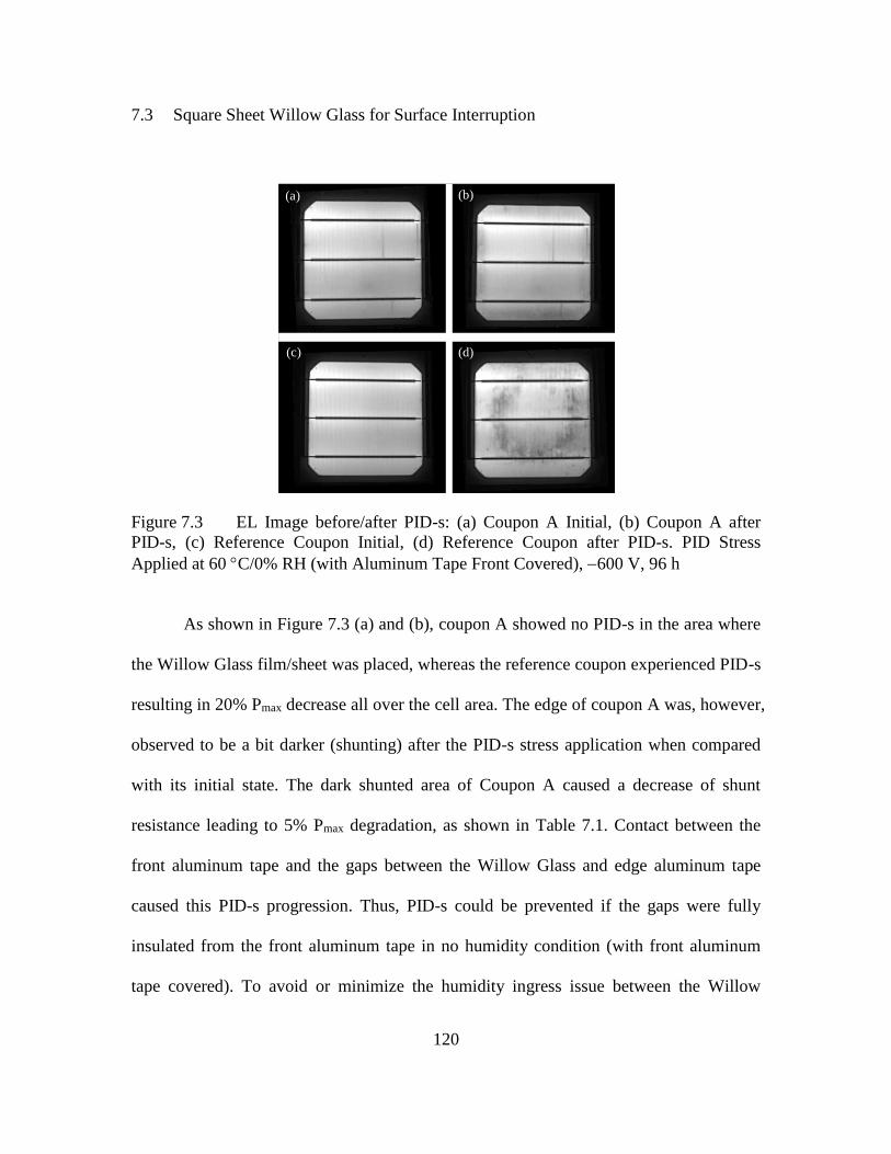
120
7.3 Square Sheet Willow Glass for Surface Interruption
Figure 7.3 EL Image before/after PID-s: (a) Coupon A Initial, (b) Coupon A after
PID-s, (c) Reference Coupon Initial, (d) Reference Coupon after PID-s. PID Stress
Applied at 60 C/0% RH (with Aluminum Tape Front Covered), 600 V, 96 h
As shown in Figure 7.3 (a) and (b), coupon A showed no PID-s in the area where
the Willow Glass film/sheet was placed, whereas the reference coupon experienced PID-s
resulting in 20% Pmax decrease all over the cell area. The edge of coupon A was, however,
observed to be a bit darker (shunting) after the PID-s stress application when compared
with its initial state. The dark shunted area of Coupon A caused a decrease of shunt
resistance leading to 5% Pmax degradation, as shown in Table 7.1. Contact between the
front aluminum tape and the gaps between the Willow Glass and edge aluminum tape
caused this PID-s progression. Thus, PID-s could be prevented if the gaps were fully
insulated from the front aluminum tape in no humidity condition (with front aluminum
tape covered). To avoid or minimize the humidity ingress issue between the Willow
(a) (b)
(c) (d)

121
Glass and module glass, the Willow Glass could be fixed with an interpenetrating
bonding material, for example an ionomer as indicated in Section 7.5.
Table 7.1 Cell Parameter before and after PID-s Stress Testing
Pmax (W) FF (%) Rshunt ()
Coupon A Initial 3.87 70.4 221
PID 96h 3.68 67.6 9.01
Reference
Coupon
Initial 3.79 70.4 252
PID 96h 3.03 58.3 1.01
Because Willow Glass is thin, light weight, and has acceptable transmittance and
exceptionally lower conductivity than common soda-lime glass, it can be applied not only
on the front surface of the PV module glass (Coupon A) but also underneath the glass
(Coupon B), as shown in Figure 7.2 (b). PID-s stressing was carried out on this one-cell
coupon (Coupon B) under 60 °C/85% RH, −600 V conditions for 96 h. In addition, a
PID-s-free EVA one-cell coupon (with no Willow Glass but commercially available PID-
s-free EVA instead of common EVA) also was PID-s stressed to compare the PID-s-
resistance. Whereas coupon B showed extremely strong PID-s-resistance, the PID-s-free
EVA coupon (“Coupon B-2”) suffered from PID-s that resulted in more than a 10%
power decrease, as shown in Figure 7.4. We also performed a PID-s test for a coupon
having a commercially available PID-s-free cell with regular EVA, and even this cell
exhibited PID-s with a power loss greater than 30% in 96 h. These alleged PID-s-free
EVA and cells would both fail the PID draft standard [51]. It is possible that the failure of
these PID-s-free EVA and cells might be attributed to non-optimized lamination

122
conditions for those components. Nevertheless, it is suggested that PID-s-free EVA/cells
available in the open market should be carefully evaluated when replacing the existing
components to safely avoid PID-s.
(a)
(b)
Figure 7.4 PID-s Progress under 60 °C/85% RH, −600 V for 96 h: (a) A Coupon with
the Willow Glass, (b) A Coupon with PID-s-Free EVA (no Willow Glass).
Table 7.2 Cell Parameter Relative Differences Due to The Additional Willow Glass
Sheet and EVA Layer
Isc
(%)
Voc
(%)
Imp
(%)
Vmp
(%)
Pmax
(%)
FF
(%)
Efficiency
(%)
Before
PID −1.71 −0.00 −1.46 −0.48 −1.95 −0.14 −1.96
After
PID 96h 0.74 0.34 0.17 0.77 0.95 −0.14 0.92

123
It was expected that adding an additional EVA layer and the Willow Glass
between the solar glass and the cell might result in a decrease in the transmittance. The
first row in Table 7.2 shows the cell performance loss due to the additional layers in the
coupon before PID-s stressing. The data comprising this row was created by measuring I–
V performance of nearly identical cells before and after lamination. The decrease of
transmittance before PID-s stressing due to the additional layers causes short circuit
current (Isc) loss, which results in an efficiency loss (−2% before PID-s). Interestingly, the
efficiency (relative) was rather improved from −2% to 1% due to an Isc increase after the
96-h PID-s stress. It is suspected that the test condition (60 °C and 96 h) leads to
transmittance improvement of the EVA, which could be caused by better curing of the
EVA. Also, a freshness of the EVA could affect the lamination quality as the
manufacturer states in the specification sheet. There were limitations in keeping the EVA
fresh in ASU Solar Power Laboratory since our laboratory was not designed for
commercial PV manufacturing. This might suggest that the lamination process should be
optimized to minimize Isc loss or even improve Isc when the Willow Glass is applied
below the PV module glass.
The method used in Coupon A and B showed great PID resistance using the
Willow Glass. However, Coupon B method has a few disadvantages in applying them on
the PV modules operating in a real field. First, overall output power will decrease due to
a lower transmittance from additional bonding layer and Willow Glass. Secondly, cost
could be considerably higher when the Willow Glass covering all the cells in a PV
module is used on the PV module surface or placed between the module glass and an
additional EVA. The Coupon B method requiring large surface area of Willow Glass

124
could lead to marginal or considerable increase in the module manufacturing cost as
compared to the other method using alternative encapsulant materials proven to be PID-
resistant, such as polyolefin [70, 118-120] or ionomer [68, 69], due to additional process
and materials. In order to address these issues, the amount of these additional materials
covering the cells/module should be minimized. These issues are addressed by using edge
interruption method using Willow Glass strips, which is presented in Sections 7.4 and 7.5.
The edge interruption method which is used in Coupon C is much more cost effective
than Coupon A or B since the required area of Willow Glass is much less than 10% of the
additional material used in Coupon A or B. Moreover, there is no transmittance loss on to
the cells since the strips are applied only around the module edges. Therefore, we
anticipate that the Coupon C method should have a higher market penetration as
compared to the Coupon B method.
An illustrative PID-s circuit with high humidity or rain for the field-installed PV
modules can be drawn as shown in Figure 7.5. The surface interruption method
demonstrated in this section is maximized by increasing the Rfront surface as
schematically depicted in the circuit diagram shown in Figure 7.5. Willow Glass above
the coupon glass provides an extremely high Rfront surface, which interrupted PID-s. The
Willow glass below the coupon glass also increases the resistance between the front glass
and the cell so that PID-s is interrupted. In the literature, it has been reported that PID-s
can be prevented/reduced by increasing Rglass [19, 73] or Rencapsulant [32, 69, 70]. An
advantage of using the Willow Glass when compared with these PID-s prevention
techniques is that there is no need to change potentially PID-s-susceptible PV module
materials or cells, which are already used in the module construction. PID-s could be

125
simply minimized or eliminated even after manufacturing the modules, by simply adding
the thin flexible Willow Glass in the PV module structure/construction. In other words,
Willow Glass can be used as an insulating or PID-s circuit interrupting barrier to block
sodium transport to the cells even if common soda-lime glass is used or PID-s-susceptible
cell is used in the module structure.
Figure 7.5 Cross-section of Typical PV Module that shows the Resistance of PV
Module Materials Affecting PID-s-Susceptibility.
7.4 Rectangular Strip Willow Glass for Edge Interruption
Using a conceptual setup, previous researchers of this research group reported that
PID-s can be prevented or mitigated by interrupting the surface continuity near the frame
edge of the PV module [121, 122]. In this method, the circuit shown in Figure 7.5 is
conceptually interrupted by a very high value of Redge, thereby preventing PID-s without
any transmittance loss to the cells as they are attached away from the cell at the frame

126
edge. To prove this conceptual approach through the use of a physical material as a
circuit interrupter, we applied Willow Glass strips/films to a one-cell coupon to increase
the Redge. A portion of the Willow Glass strip was fixed by edge aluminum tape (see
Figure 7.2 (c)); thus, the Willow Glass was in direct contact with the coupon glass. The
results shown in Figure 7.6 and Figure 7.7 indicate that PID-s can be physically
prevented due to near-edge surface disruption caused by the Willow Glass strips. Coupon
C showed nearly no degradation in terms of maximum power (Pmax), whereas the Pmax of
the reference coupon showed a power loss of 10% at standard test conditions (STC) and
40% at low irradiance, as shown in Figure 7.7 (c). It should be noted that the bottom of
the cell in coupon C was slightly affected by PID-s, as shown in the EL image in Figure
7.6 (b). In that area, there was a decrease of about 55% in shunt resistance (Rsh), as shown
in Figure 7.7 (c). These effects were caused by the unintended conductive path resulting
from water ingress between the Willow Glass and the coupon glass during the PID-s
stress test. This conductive path can be prevented by avoiding the water ingress with the
use of an improved method presented in Section 7.5 for affixing the Willow Glass at the
edges of the coupon glass.

127
Figure 7.6 EL Image before/after PID-s: (a) Coupon C Initial, (b) Coupon C after
PID-s, (c) Reference Coupon Initial, (d) Reference Coupon after PID-s.
(a) (b)
(c)
Figure 7.7 I–V Results before/after PID: (a) Coupon C, (b) Reference Coupon, (c)
Several Important I–V Parameters Regarding PID.
(a) (b)
(d)(c)

128
7.5 Ionomer Bonded Willow Glass Strip for Edge Interruption
Since the edge interruption method in preventing PID-s was proved to be working,
it was expected that any high Redge materials that are interrupting the circuit should work
as well. One of the candidates studied was a hydrophobic material, which could interrupt
the circuit by repelling water near the coupon edges. The hydrophobic material chosen
from two different manufacturers was sprayed around the edges of two coupons, and then
PID-s stressing was carried out at 60 °C/85% RH, −600 V for 5 h. Both coupons
exhibited PID-s. This could be attributable to pinholes or cracks in the hydrophobic layer,
as shown in Figure 7.8. The 85% RH in a weathering chamber is maintained by mist, and
the mist could possibly permeate into the pinholes/cracks, which facilitate creating a
conducting path to the front coupon glass. It is suggested that the hydrophobic materials
for the edge interruption method should not have those defects to effectively prevent
PID-s if they are applied to module edges. Electrical insulating spray was also tried to
increase the Redge. According to the manufacturer of the insulating spray, it is not
hydrophobic, but it is used to protect surfaces against weather, moisture, corrosion, oil,
alkalies, and acids. The aforementioned PID-s stress conditions were applied to the
coupon with the insulating spray, and it was determined that this material also did not
work in preventing PID-s. It showed a rather stronger degradation in power than the
coupon with the hydrophobic layer. It is suspected that the insulating layer created by
spraying also has the pinholes. Another material we found for this edge interruption
method was ionomer. The ionomer has a high bulk resistivity and has been known as a
good insulation material for PV modules [69]. Ionomer strips the same size as the Willow
Glass strips were applied around the one-cell coupon edges using the PV module

129
laminator. After PID-s stressing at 60 °C/85% RH, −600 V for 5 h, the coupon showed
only 1% power decrease while a coupon having no edge interruption showed a power
decrease >10%. The ionomer strip was then used as a bonding material in fixing the
Willow Glass strip onto the coupon glass. PID-s results of the coupon with Willow Glass
bonded by a thin ionomer layer showed only approximately 1% power decrease. As
shown in Figure 7.9, there are nearly no changes in I–V curves and no significant
shunting spots based on EL images. It is expected that the Willow Glass strip with
ionomer would provide reliable PID-s prevention since the Willow Glass provides a
hermetic good barrier for the well-demonstrated Willow Glass circuit interrupter. In
addition, the Willow Glass protects the ionomer from deterioration caused by direct
atmosphere exposure, such as UV, humidity and soiling. However, application of Coupon
C method in the field would be challenging as it currently requires a lamination process
of Willow Glass strips with underlying ionomer layer. It is, therefore, anticipated that the
application of Coupon C method in the field without lamination process requires
additional research to successfully implement this method in the field. Nevertheless, this
work still demonstrates that the ionomer bonded Willow Glass strips near the frame
edges on the glass surface can prevent the PID-s in the long term field conditions through
the removal of conductive path resulting from water ingress between Willow Glass and
module glass.

130
Figure 7.8 Optical Microscope Image (10x) Showing Cracks of the Hydrophobic
Layer Sprayed around the One-Cell Coupon Edges.
(a)
(b) (c)
Figure 7.9 PID-s Test Results of the Coupon with Willow Glass + Ionomer: (a) I–V
Results before/after PID-s, (b) EL Image before PID-s, (c) EL Image after PID-s.

131
7.6 Summary
In this chapter, we present a simple method that uses thin flexible/film Corning®
Willow® Glass on the surface of the glass superstrate to prevent PID-s. Adding a Willow
Glass layer onto the glass superstrate effectively minimized or eliminated PID-s. One of
innovative advantages is that Willow Glass could be applied onto the glass superstrates of
modules not only during manufacturing but also in the field by taking advantage of edge
interruption. Currently manufactured PV modules are expected to mostly contain the
PID-s-free cells but a large fraction of the p-base crystalline silicon PV modules installed
over the last 10 years might have a potential susceptibility to PID-s. Applying this edge
interruption method to those field-installed modules would be a simple and low-cost way
to prevent or minimize PID-s progression. The surface disruption method presented in
this work was demonstrated to be effective. Further experiments are in progress to apply
this method to full-size commercial PV modules.

132
Chapter 8
CONCLUSION AND FUTURE WORK
8.1 Conclusion
In this dissertation, various characteristics of PID, especially recovery
characteristics, were studied. No complete recovery in terms of power at low irradiance,
shunt resistance, and QE at short wavelength was achieved regardless of recovery
methods, such as applying high temperature or reverse potential, although power at
standard test condition (high irradiance) showed near full recovery. Low recovery of
shunt resistance in PID-affected solar cells could cause detrimental effects to the modules
if the cells in a module were to operate under shaded/reverse-bias condition with failed
bypass diodes. Therefore, this work recommends that the type of PID recovery method
should be carefully investigated as a long-term solution to modules exhibiting PID. QE
loss, which could be one of the PID effects in the short wavelength range, was modelled
by increasing the front surface recombination velocity and verified by QE measurements
on bare cells, and this was carried out utilizing a new PID testing method using cells that
had not gone through a lamination process.
At the cell level, PID could be avoided by the use of high phosphorous
concentration emitters (low sheet resistance: ~ 60 Ω/sq) even if the SiNx ARC is PID-
susceptible in p-type crystalline silicon solar cells. Also, PID-susceptible cells can be
screened by using ILIT with simplified sample structure during the cell fabrication
process. At the module level, PID could be prevented by a leakage current circuit
disruption method. The circuit was effectively interrupted by using either Corning
Willow Glass sheets or Corning Willow Glass strips. The Willow Glass sheets could be

133
applied below the module glass or above the module glass during the module
manufacturing process. A PV module having a Willow Glass strip attached peripherally
around the module edges showed no PID as well as no transmittance loss while the one
incorporating a blanket Willow Glass sheet has exhibited transmittance loss. This method
can be applied to eliminate the PID issue in the PID-susceptible crystalline silicon PV
modules already installed in a field. Therefore, there is no need to replace those modules
from the field to avoid PID in future.
8.2 Future Work
The effect of the surface phosphorous concentration in the emitter on PID has
been presented in this dissertation. Cells with high surface phosphorous concentration
emitters clearly prevented or delayed the PID progress while ones with low surface
phosphorous concentration emitters experienced PID. However, it is unclear how it
physically works. For the emitter analysis, PID-susceptible (low surface phosphorous
concentration emitter) cells fabricated from semiconductor polished wafers for SIMS and
ECV measurements were PID stressed; however, no clear PID was observed. Therefore,
surface analysis for cells fabricated by textured solar wafers are needed, but it is
challenging to measure SIMS or ECV on textured solar cells. The PID prevention method
using the Willow Glass strip has been demonstrated for one-cell laminated coupons. It is
recommended to apply the PID prevention based upon Willow Glass strips to
commercial-size PV modules.

134
REFERENCES
[1] A. E. Becquerel, "Mémoire sur les effets électriques produits sous l'influence des
rayons solaires," Comptes Rendus, vol. 9, pp. 561-567, 1839.
[2] Photovoltaics report [Online]. Available:
https://www.ise.fraunhofer.de/de/downloads/pdf-files/aktuelles/photovoltaics-
report-in-englischer-sprache.pdf
[3] Average annual temperature [Online]. Available:
https://nelson.wisc.edu/sage/data-and-
models/atlas/maps.php?datasetid=35&includerelatedlinks=1&dataset=35
[4] Average annual relative humidity [Online]. Available:
https://nelson.wisc.edu/sage/data-and-
models/atlas/maps.php?datasetid=53&includerelatedlinks=1&dataset=53
[5] E. Bournay. The global solar uv index [Online]. Available:
http://www.grida.no/graphicslib/detail/the-global-solar-uv-index_1394
[6] M. Woodhouse, T. James, R. Margolis, D. Feldman, T. Merkel, and A. Goodrich,
"An economic analysis of photovoltaics versus traditional energy sources: Where
are we now and where might we be in the near future?," in Proc. 37th IEEE
Photovoltaic Spec. Conf., 2011, pp. 2481-2483.
[7] M. Woodhouse, A. Goodrich, T. James, R. Margolis, D. Feldman, and T. Markel.
An economic analysis of photovoltaics versus traditional energy sources: Where
are we now and where might we be in the near future?, Sildes [Online]. Available:
http://www.nrel.gov/docs/fy11osti/52311.pdf
[8] D. Chung, C. Davidson, R. Fu, K. Ardani, and R. Margolis, "U.S. Photovoltaic
prices and cost breakdowns: Q1 2015 benchmarks for residential, commercial,
and utility-scale systems," Naional Renewable Energy Laboratory NREL/TP-
6A20-64746, 2015.
[9] M. Kontges, S. Kurtz, C. Packard, U. Jahn, K. A. Berger, K. Kato, T. Friesen, H.
Liu, and M. V. Iseghem, "Review of failures of photovoltaic modules,"
International Energy Agency (IEA) IEA-PVPS T13-01:2014, 2014.
[10] A. Ndiaye, A. Charki, A. Kobi, C. M. F. Kébé, P. A. Ndiaye, and V. Sambou,
"Degradations of silicon photovoltaic modules: A literature review," Solar Energy,
vol. 96, pp. 140-151, 2013.
[11] D. L. King, M. A. Quintana, J. A. Kratochvil, D. E. Ellibee, and B. R. Hansen,
"Photovoltaic module performance and durability following long-term field
exposure," Prog. Photovoltaic Res. Appl, vol. 8, pp. 241-256, 2000.

135
[12] T. Shioda, "Delamination failures in long-term field-aged PV modules from point
of view of encapsulant," in Proc. Photovoltaic Module Reliab. Workshop, 2013.
[13] M. A. Quintana, D. L. King, T. J. McMahon, and C. R. Osterwald, "Commonly
observed degradation in field-aged photovoltaic modules," in Proc. 29th IEEE
Photovoltaic Spec. Conf., 2002, pp. 1436-1439.
[14] J. Wohlgemuth, D. W. Cunningham, A. Nguyen, G. Kelly, and D. Amin, "Failure
modes of crystalline Si modules," in Proc. Photovoltaic Module Reliab.
Workshop, 2010.
[15] N. G. Dhere, "Reliability issues of crystalline silicon PV modules: A review," in
14th Workshop on Crystalline Silicon Solar Cells & Modules: Materials and
Processes, 2004, pp. 39-50.
[16] M. Rekinger, F. Thies, G. Masson, and S. Orlandi. Global market outlook for
solar power 2015-2019 [Online]. Available:
http://www.solarpowereurope.org/insights/global-market-outlook/
[17] G. Mon, J. Orehotsky, R. Ross, and G. Whitla, "Predicting electrochemical
breakdown in terrestrial photovoltaic modules," in Proc. 17th IEEE Photovoltaic
Spec. Conf., Kissimmee, FL, USA, 1984, pp. 682-692.
[18] G. R. Mon, G. Whitla, R. Ross, and M. Neff, "The role of electrical insulation in
electrochemical degradation of terrestrial photovoltaic modules," Electrical
Insulation, IEEE Transactions on, vol. EI-20, pp. 989-996, 1985.
[19] P. Hacke, M. Kempe, K. Terwilliger, S. Glick, and S. Kurtz, "Characterization of
multicrystalline silicon modules with system bias voltage applied in damp heat,"
in Proc. 25th Eur. Photovoltaic Solar Energy Conf. Exhib./5th World Conf.
Photovoltaic Energy Convers., Valencia, Spain, 2010, pp. 3760-3765.
[20] J. Berghold, M. Roericht, A. Bottcher, S. Wendlandt, M. Hanusch, S. Koch, P.
Grunow, and B. Stegemann, "Electrochemical corrosion within solar panels," in
Proc. 27th Eur. Photovoltaic Solar Energy Conf. Exhib., 2012, pp. 3511-3517.
[21] P. Hacke, K. Terwilliger, S. Glick, D. Trudell, N. Bosco, S. Johnston, and S.
Kurtz, "Test-to-failure of crystalline silicon modules," in Proc. 35th IEEE
Photovoltaic Spec. Conf., Honolulu, HI, USA, 2010, pp. 244-250.
[22] P. Hacke, R. Smith, K. Terwilliger, S. Glick, D. Jordan, S. Johnston, M. Kempe,
and S. Kurtz, "Testing and analysis for lifetime prediction of crystalline silicon
PV modules undergoing degradation by system voltage stress," in Proc. 38th
IEEE Photovoltaic Spec. Conf., Austin, TX, USA, 2012, pp. 1750-1755.
[23] P. Hacke, R. Smith, K. Terwilliger, S. Glick, D. Jordan, S. Johnston, M. Kempe,
and S. Kurtz, "Testing and analysis for lifetime prediction of crystalline silicon
136
PV modules undergoing degradation by system voltage stress," IEEE J.
Photovoltaics, vol. 3, pp. 246-253, 2013.
[24] G. R. Mon and J. Ross, R G, "Electrochemical degradation of amorphous-silicon
photovoltaic modules," in Proc. 18th IEEE Photovoltaic Spec. Conf., Las Vegas,
NV, USA, 1985, pp. 1142-1149.
[25] C. R. Osterwald, T. J. McMahon, and J. A. del Cueto, "Electrochemical corrosion
of SnO2:F transparent conducting layers in thin-film photovoltaic modules," Sol.
Energy Mater. Sol. Cells, vol. 79, pp. 21-33, 2003.
[26] G. Mon, L. Wen, J. Ross, R G, and D. Adent, "Effects of temperature and
moisture on module leakage currents," in Proc. 18th IEEE Photovoltaic Spec.
Conf., Las Vegas, NV, USA, 1985, pp. 1179-1185.
[27] R. Swanson, M. Cudzinovic, D. DeCeuster, V. Desai, J. Jurgens, N. Kaminar, W.
Mulligan, L. Rodrigues-Barbosa, D. Rose, D. Smith, A. Terao, and K. Wilson,
"The surface polarization effect in high-efficiency silicon solar cells," in Proc.
15th Photovoltaic Solar Energy Conf., Shanghai, China, 2005.
[28] S. Pingel, O. Frank, M. Winkler, S. Daryan, T. Geipel, H. Hoehne, and J.
Berghold, "Potential induced degradation of solar cells and panels," in Proc. 35th
IEEE Photovoltaic Spec. Conf., Honolulu, HI, USA, 2010, pp. 2817-2822.
[29] J. A. del Cueto and T. J. McMahon, "Analysis of leakage currents in photovoltaic
modules under high-voltage bias in the field," Prog. Photovoltaic Res. Appl, vol.
10, pp. 15-28, 2002.
[30] M. Schutze, M. Junghanel, O. Friedrichs, R. Wichtendahl, M. Scherff, J. Muller,
and P. Wawer, "Investigations of potential induced degradation of silicon
photovoltaic modules " in 26th Eur. Photovoltaic Solar Energy Conf. Exhib.,
Hamburg, Germany, 2011, pp. 3097-3102.
[31] S. Koch, C. Seidel, P. Grunow, S. Krauter, and M. Schoppa, "Polarization effects
and tests for crystalline silicon cells," in 26th Eur. Photovoltaic Solar Energy
Conf. Exhib., Hamburg, Germany, 2011, pp. 1726-1731.
[32] S. Koch, J. Berghold, O. Okoroafor, S. Krauter, and P. Grunow, "Encapsulation
influence on the potential induced degradation of crystalline silicon cells with
selective emitter structures," in Proc. 27th Eur. Photovoltaic Solar Energy Conf.
Exhib., Frankfurt, Germany, 2012, pp. 1991-1995.
[33] P. Hacke, K. Terwilliger, R. Smith, S. Glick, J. Pankow, M. Kempe, S. K. I.
Bennett, and M. Kloos, "System voltage potential-induced degradation
mechanisms in PV modules and methods for test," in Proc. 37th IEEE
Photovoltaic Spec. Conf., Seattle, WA, USA, 2011, pp. 814-820.

137
[34] M. Schutze, M. Junghanel, M. B. Koentopp, S. Cwikla, S. Friedrich, J. W. Muller,
and P. Wawer, "Laboratory study of potential induced degradation of silicon
photovoltaic modules," in Proc. 37th IEEE Photovoltaic Spec. Conf., Seattle, WA,
USA, 2011, pp. 821-826.
[35] V. Naumann, D. Lausch, A. Hähnel, J. Bauer, O. Breitenstein, A. Graff, M.
Werner, S. Swatek, S. Großer, J. Bagdahn, and C. Hagendorf, "Explanation of
potential-induced degradation of the shunting type by Na decoration of stacking
faults in Si solar cells," Sol. Energy Mater. Sol. Cells, vol. 120, Part A, pp. 383-
389, 2014.
[36] H. Nagel, A. Metz, and K. Wangemann, "Crystalline Si solar cells and modules
featuring excellent stability against potential-induced degradation," in 26th Eur.
Photovoltaic Solar Energy Conf. Exhib., Hamburg, Germany, 2011, pp. 3107-
3112.
[37] S. Koch, D. Nieschalk, J. Berghold, S. Wendlandt, S. Krauter, and P. Grunow,
"Potential induced degradation effects on crystalline silicon cells with various
antireflective coatings," in Proc. 27th Eur. Photovoltaic Solar Energy Conf.
Exhib., Frankfurt, Germany, 2012, pp. 1985-1990.
[38] D. E. Carlson, R. Romero, F. Willing, D. Meakin, L. Gonzalez, R. Murphy, H. R.
Moutinho, and M. Al-Jassim, "Corrosion effects in thin-film photovoltaic
modules," Prog. Photovoltaic Res. Appl, vol. 11, pp. 377-386, 2003.
[39] V. Naumann, C. Hagendorf, S. Grosser, M. Werner, and J. Bagdahn, "Micro
structural root cause analysis of potential induced degradation in c-Si solar cells,"
Energy Procedia, vol. 27, pp. 1-6, 2012.
[40] J. Bauer, V. Naumann, S. Großer, C. Hagendorf, M. Schütze, and O. Breitenstein,
"On the mechanism of potential-induced degradation in crystalline silicon solar
cells," Phys. Status Solidi: Rapid Res. Lett, vol. 6, pp. 331-333, 2012.
[41] V. Naumann, D. Lausch, S. Großer, M. Werner, S. Swatek, C. Hagendorf, and J.
Bagdahn, "Microstructural analysis of crystal defects leading to potential-induced
degradation (PID) of Si solar cells," Energy Procedia, vol. 33, pp. 76-83, 2013.
[42] V. Naumann, D. Lausch, A. Graff, M. Werner, S. Swatek, J. Bauer, A. Hähnel, O.
Breitenstein, S. Großer, J. Bagdahn, and C. Hagendorf, "The role of stacking
faults for the formation of shunts during potential-induced degradation of
crystalline Si solar cells," Phys. Status Solidi: Rapid Res. Lett, vol. 7, pp. 315-318,
2013.
[43] D. Lausch, V. Naumann, O. Breitenstein, J. Bauer, A. Graff, J. Bagdahn, and C.
Hagendorf, "Potential-induced degradation (PID): Introduction of a novel test
approach and explanation of increased depletion region recombination," IEEE J.
Photovoltaics, vol. 4, pp. 834-840, 2014.

138
[44] A. Colli, "The role of sodium in photovoltaic devices under high voltage stress: A
holistic approach to understand unsolved aspects," Renewable Energy, vol. 60, pp.
162-168, 2013.
[45] M. Wilson, A. Savtchouk, P. Edelman, D. Marinskiy, and J. Lagowski, "Drift
characteristics of mobile ions in SiNx films and solar cells," Sol. Energy Mater.
Sol. Cells, vol. 142, pp. 102-106, 2015.
[46] C. Taubitz, M. Schutze, and M. B. Koentopp, "Towards a kinetic model of
potential-induced shunting," in Proc. 27th Eur. Photovoltaic Solar Energy Conf.
Exhib., Frankfurt, Germany, 2012, pp. 3172-3176.
[47] B. Ziebarth, M. Mrovec, C. Elsässer, and P. Gumbsch, "Potential-induced
degradation in solar cells: Electronic structure and diffusion mechanism of
sodium in stacking faults of silicon," J. Appl. Phys., vol. 116, p. 093510, 2014.
[48] D. Lausch, V. Naumann, A. Graff, A. Hähnel, O. Breitenstein, C. Hagendorf, and
J. Bagdahn, "Sodium outdiffusion from stacking faults as root cause for the
recovery process of potential-induced degradation (PID)," Energy Procedia, vol.
55, pp. 486-493, 2014.
[49] IEC, "Crystalline silicon terrestrial photovoltaic (PV) modules - design
qualification and type approval," ed: IEC 61215 Ed. 2 2005.
[50] P. Hacke, R. Smith, K. Terwilliger, G. Perrin, B. Sekulic, and S. Kurtz,
"Development of an IEC test for crystalline silicon modules to qualify their
resistance to system voltage stress," Prog. Photovoltaic Res. Appl, vol. 22, pp.
775-783, 2014.
[51] IEC, "System voltage durability test for crystalline silicon modules - qualification
and type approval," ed: IEC 62804 Ed. 1.0 draft standard
[52] S. Pingel, S. Janke, and O. Frank, "Recovery methods for modules affected by
potential induced degradation (PID)," in Proc. 27th Eur. Photovoltaic Solar
Energy Conf. Exhib., Frankfurt, Germany, 2012, pp. 3379-3383.
[53] J. Hattendorf, R. Loew, W. M. Gnehr, L. Wulff, M. C. Koekten, D. Koshnicharov,
A. Blauaermel, and J. A. Esquivel, "Potential induced degradation in mono-
crystalline silicon based modules: An acceleration model," in Proc. 27th Eur.
Photovoltaic Solar Energy Conf. Exhib., Frankfurt, Germany, 2012, pp. 3405-
3410.
[54] S. Hoffmann and M. Koehl, "Influence of humidity and temperature on the
potential induced degradation," in Proc. 27th Eur. Photovoltaic Solar Energy
Conf. Exhib., Frankfurt, Germany, 2012, pp. 3148-3151.

139
[55] A. Raykov, H. Nagel, D.-J. Amankwah, and W. Bergholz, "Climate model for
potential-induced degradation of crystalline silicon photovoltaic modules," in
Proc. 27th Eur. Photovoltaic Solar Energy Conf. Exhib., Frankfurt, Germany,
2012, pp. 3399-3404.
[56] P. Hacke, P. Burton, A. Hendrickson, S. Spataru, S. Glick, and K. Terwilliger,
"Effects of photovoltaic module soiling on glass surface resistance and potential-
induced degradation," in Proc. 42nd IEEE Photovoltaic Spec. Conf., 2015, pp. 1-4.
[57] P. Hacke, "Testing modules for potential-induced degradation – a status update of
IEC 62804," in Proc. Photovoltaic Module Reliab. Workshop, 2014.
[58] J. Bagdahn, M. Ebert, J. Frobel, and S. Dietrich, "Test results of potential induced
degradation (PID) of solar modules from different manufacturers," Fraunhofer
Center for Silicon Photovoltaics CSP, 2012.
[59] J. Berghold, O. Frank, H. Hoehne, S. Pingel, B. Richardson, and M. Winkler,
"Potential induced degradation of solar cells and panels," in Proc. 25th Eur.
Photovoltaic Solar Energy Conf. Exhib./5th World Conf. Photovoltaic Energy
Convers., Valencia, Spain, 2010, pp. 3753-3759.
[60] K. Mishina, A. Ogishi, K. Ueno, T. Doi, K. Hara, N. Ikeno, D. Imai, T.
Saruwatari, M. Shinohara, T. Yamazaki, A. Ogura, Y. Ohshita, and A. Masuda,
"Investigation on antireflection coating for high resistance to potential-induced
degradation," Jpn. J. Appl. Phys., vol. 53, p. 03CE01, 2014.
[61] K. Mishina, A. Ogishi, K. Ueno, S. Jonai, N. Ikeno, T. Saruwatari, K. Hara, A.
Ogura, T. Yamazaki, T. Doi, and A. Masuda, "Anti-reflection coating with high
PID-resistance for crystalline silicon solar cells " in Proc. 29th Eur. Photovoltaic
Sol. Energy Conf. Exhib, Amsterdam, Netherlands, 2014, pp. 996-999.
[62] H. Mehlich, D. Decker, U. Scheit, M. Uhlig, S. Frigge, M. Runge, B. Heinze, H. P.
Sperrlich, J. Mai, H. Schlemm, E. Vetter, J. Hohne, S. Reichel, and W. Stein, "A
new method for high resistance against potential induced degradation," in Proc.
27th Eur. Photovoltaic Solar Energy Conf. Exhib., Frankfurt, Germany, 2012, pp.
3411-3413.
[63] W. Han, W. Shan, S. Liu, W. Li, X. Niu, J. Jin, C. L. J. Li, and Q. Zhai, "Ion
implantation - an effective solution to prevent c-Si PV module PID," in Proc. 28th
Eur. Photovoltaic Sol. Energy Conf. Exhib, Paris, France, 2013, pp. 3309-3312.
[64] S. Basame, Q. Zhai, T. Thanigaivelan, Y. Maruyama, and H. Naritomi, "Ion
implanted high efficiency PID free cells for today’s solar market," in Proc. 28th
Eur. Photovoltaic Sol. Energy Conf. Exhib, Paris, France, 2013, pp. 1197-1200.
[65] H. Nagel, P. Saint-Cast, M. Glatthaar, and S. W. Glunz, "Inline processes for the
stabilization of p-type crystalline Si solar cells against potential-induced

140
degradation," in Proc. 29th Eur. Photovoltaic Sol. Energy Conf. Exhib,
Amsterdam, Netherlands, 2014, pp. 2351-2355.
[66] C.-H. Du, C.-H. Chen, C.-H. Lung, S.-Y. Chen, L.-Y. Li, Y.-H. Lin, and J. A.
Yeh, "A well-controlled PSG layer on silicon solar cells against potential induced
degradation," ECS Journal of Solid State Science and Technology, vol. 4, pp. 97-
100, 2015.
[67] I. Périchaud, "Gettering of impurities in solar silicon," Sol. Energy Mater. Sol.
Cells, vol. 72, pp. 315-326, 2002.
[68] S. C. Pop, R. Schulze, X. Wang, B. Yuan, J. Kapur, K. Stika, C. Westphal, H.
Antoniadis, and A. Meisel, "Ionomer-based PID-resistant encapsulant for PV
modules," in Proc. 29th Eur. Photovoltaic Sol. Energy Conf. Exhib, Amsterdam,
Netherlands, 2014, pp. 152-157.
[69] J. Kapur, K. M. Stika, C. S. Westphal, J. L. Norwood, and B. Hamzavytehrany,
"Prevention of potential-induced degradation with thin ionomer film," IEEE J.
Photovoltaics, vol. 5, pp. 219-223, 2015.
[70] M. C. López-Escalante, L. J. Caballero, F. Martín, M. Gabás, A. Cuevas, and J. R.
Ramos-Barrado, "Polyolefin as PID-resistant encapsulant material in PV
modules," Sol. Energy Mater. Sol. Cells, vol. 144, pp. 691-699, 2016.
[71] 3M. Solar encapsulant film [Online]. Available:
http://solutions.3m.com/wps/portal/3M/en_US/Renewable/Energy/Product/Films/
Solar-Encapsulant-Film/
[72] K. Hara, S. Jonai, and A. Masuda, "Crystalline Si photovoltaic modules
functionalized by a thin polyethylene film against potential and damp-heat-
induced degradation," RSC Advances, vol. 5, pp. 15017-15023, 2015.
[73] M. Kambe, K. Hara, K. Mitarai, S. Takeda, M. Fukawa, N. Ishimaru, and M.
Kondo, "PID-free c-Si PV module using aluminosilicate chemically strengthened
glass," in Proc. 28th Eur. Photovoltaic Sol. Energy Conf. Exhib, Paris, France,
2013, pp. 2861-2864.
[74] T. Kajisa, H. Miyauchi, K. Mizuhara, K. Hayashi, T. Tokimitsu, M. Inoue, K.
Hara, and A. Masuda, "Novel lighter weight crystalline silicon photovoltaic
module using acrylic-film as a cover sheet," Jpn. J. Appl. Phys., vol. 53, p.
092302, 2014.
[75] K. Hara, H. Ichinose, T. N. Murakami, and A. Masuda, "Crystalline Si
photovoltaic modules based on TiO2-coated cover glass against potential-induced
degradation," RSC Advances, vol. 4, pp. 44291-44295, 2014.

141
[76] S. C. Pop, R. Schulze, B. Brophy, S. Maghsoodi, Y. S. Yang, Z. R. Abrams, and P.
Gonsalves, "Development of an ion-barrier film on solar panel glass," in Proc.
42nd IEEE Photovoltaic Spec. Conf., New Orleans, LA, USA, 2015, pp. 1-6.
[77] T. Yoshida, Y. Fan, and Y. Kishimoto, "A novel concept and a new design for
coating materials to prevent PID as well as improve power generation efficiency,"
in Proc. 29th Eur. Photovoltaic Sol. Energy Conf. Exhib, 2014, pp. 136-139.
[78] PID - the problem and how to solve it: Module regeneration with the PV offset
box [Online]. Available: http://files.sma.de/dl/7418/PID-PVOBox-TI-en-10.pdf
[79] Panasonic. Fraunhofer institute confirms: Panasonic HIT photovoltaic modules
are PID resistant [Online]. Available: http://eu-solar.panasonic.net/presse/press-
center/article/fraunhofer-institute-confirms-panasonic-hit-photovoltaic-modules-
are-pid-resistant/
[80] N. Riedel, L. Pratt, E. Moss, and M. Yamasaki, "600 hour potential induced
degradation (PID) testing on silicon, CIGS and HIT modules," in Proc.
Photovoltaic Module Reliab. Workshop, 2015.
[81] B.-M. Meiners, S. Holinski, P. Schafer, S. Hohage, and D. Borchert,
"Investigation of anti-reflection-coating stacks for silicon heterojunction solar
cells," in Proc. 29th Eur. Photovoltaic Sol. Energy Conf. Exhib, Amsterdam,
Netherlands, 2014, pp. 1020-1023.
[82] D.-H. Neuhaus and A. Münzer, "Industrial silicon wafer solar cells," Advances in
OptoElectronics, vol. 2007, pp. 1-15, 2007.
[83] T. Ishiguro, H. Kanno, M. Taguchi, and S. Okamoto, "Study on PID resistance of
HIT® PV modules," in Proc. Photovoltaic Module Reliab. Workshop, 2013.
[84] M. Taguchi, A. Yano, S. Tohoda, K. Matsuyama, Y. Nakamura, T. Nishiwaki, K.
Fujita, and E. Maruyama, "24.7% record efficiency HIT solar cell on thin silicon
wafer," IEEE J. Photovoltaics, vol. 4, pp. 96-99, 2014.
[85] V. Naumann, T. Geppert, S. Großer, D. Wichmann, H.-J. Krokoszinski, M.
Werner, and C. Hagendorf, "Potential-induced degradation at interdigitated back
contact solar cells," Energy Procedia, vol. 55, pp. 498-503, 2014.
[86] A. Halm, A. Schneider, V. D. Mihailetchi, L. J. Koduvelikulathu, L. M. Popescu,
G. Galbiati, H. Chu, and R. Kopecek, "Potential-induced degradation for
encapsulated n-type IBC solar cells with front floating emitter," Energy Procedia,
vol. 77, pp. 356-363, 2015.
[87] K. Hara, S. Jonai, and A. Masuda, "Potential-induced degradation in photovoltaic
modules based on n-type single crystalline Si solar cells," Sol. Energy Mater. Sol.
Cells, vol. 140, pp. 361-365, 2015.

142
[88] V. Fjällström, P. M. P. Salomé, M. Edoff, T. Jarmar, B. G. Aitken, K. Zhang, K.
Fuller, and C. K. Williams, "Potential-induced degradation of CuIn1-xGaxSe2
thin film solar cells," IEEE J. Photovoltaics, vol. 3, pp. 1090-1094, 2013.
[89] V. Fjällström, P. Szaniawski, B. Vermang, P. M. P. Salomé, F. Rostvall, U.
Zimmermann, and M. Edoff, "Recovery after potential-induced degradation of
CuIn1-xGaxSe2 solar cells with CdS and Zn(O,S) buffer layers," IEEE J.
Photovoltaics, vol. 5, pp. 664-669, 2015.
[90] G. Mathiak, M. Schweiger, and W. Herrmann, "Potential-induced degradation -
comparison of different test methods and low irradiance performance
measurements," in Proc. 27th Eur. Photovoltaic Solar Energy Conf. Exhib.,
Frankfurt, Germany, 2012, pp. 3157-3162.
[91] P. Hacke, "Considerations for a standardized test for potential-induced
degradation of crystalline silicon PV modules," in Proc. Photovoltaic Module
Reliab. Workshop, 2012.
[92] J. Oh, S. Bowden, and G. Tamizhmani, "Application of reverse bias recovery
technique to address PID issue: Incompleteness of shunt resistance and quantum
efficiency recovery," in Proc. 40th IEEE Photovoltaic Spec. Conf., Denver, CO,
USA, 2014, pp. 925-929.
[93] J. Oh, G. Tamizhmani, and S. Bowden, "Scaling error of quantum efficiency
measurements for heavily shunted cells in reliability research," in Proc. 40th
IEEE Photovoltaic Spec. Conf., Denver, CO, USA, 2014, pp. 2635-2638.
[94] E. Sugimura, S. Takamoto, S. Tsujii, K. Hirata, A. Tani, and T. Fuyuki, "Spatially
resolved electroluminescence imaging of shunt sources in crystalline silicon solar
cells," Jpn. J. Appl. Phys., vol. 51, p. 10NA02, 2012.
[95] K. Bothe, K. Ramspeck, D. Hinken, C. Schinke, J. Schmidt, S. Herlufsen, R.
Brendel, J. Bauer, J.-M. Wagner, N. Zakharov, and O. Breitenstein,
"Luminescence emission from forward- and reverse-biased multicrystalline
silicon solar cells," J. Appl. Phys., vol. 106, p. 104510, 2009.
[96] B. Knisely, J. Kuitche, G. Tamizhmani, A. Korostyshevsky, and H. Field, "Non-
intrusive cell quantum efficiency measurements of accelerated stress tested
photovoltaic modules," in Proc. 40th IEEE Photovoltaic Spec. Conf., Denver, CO,
USA, 2014, pp. 1870-1874.
[97] J.-J. Li, S. H. Lim, and Y.-H. Zhang, "A novel method to eliminate the
measurement artifacts of external quantum efficiency of multi-junction solar cells
caused by the shunt effect," in Proc. SPIE 8256, San Francisco, CA, USA, 2012,
pp. 825616-1-825616-7.

143
[98] H. J. Hovel, Semiconductors and semimetals vol. 11. New York: Academic Press,
Inc, 1975, pp. 24-37.
[99] P. Saint-Cast, H. Nagel, D. Wagenmann, J. Schon, P. Schmitt, C. Reichel, S. W.
Glunz, M. Hofmann, J. Rentsch, and R. Preu, "Potential-induced degradation on
cell level: The inversion model," in Proc. 28th Eur. Photovoltaic Sol. Energy
Conf. Exhib, Paris, France, 2013, pp. 789-792.
[100] R. Haberecht, M. Junghanel, R. Apelt, K. Duncker, and S. Peters, "Rapid PID-test
for unlaminated solar cells," in Proc. 28th Eur. Photovoltaic Sol. Energy Conf.
Exhib, Paris, France, 2013, pp. 1611-1614.
[101] C. Honsberg and S. Bowden. Quantum efficiency [Online]. Available:
http://pveducation.org/pvcdrom/solar-cell-operation/quantum-efficiency
[102] J. Nelson, The physics of solar cells. London, UK: Imperial College Press, 2003,
pp. 165-167.
[103] J. Oh, S. Bowden, and G. TamizhMani, "Potential-induced degradation (PID):
Incomplete recovery of shunt resistance and quantum efficiency losses," IEEE J.
Photovoltaics, vol. 5, pp. 1540-1548, 2015.
[104] V. Naumann, D. Lausch, and C. Hagendorf, "Sodium decoration of PID-s crystal
defects after corona induced degradation of bare silicon solar cells," Energy
Procedia, vol. 77, pp. 397-401, 2015.
[105] M. Wilson, A. Savthouck, J. D'Amico, J. Lagowski, S. Schmitt, A. Schneider, and
S. Olibet, "Importance of defect photoionization in silicon-rich SiNx dielectrics
for high PID resistance," in Proc. 39th IEEE Photovoltaic Spec. Conf., Tampa, FL,
USA, 2013, pp. 218-222.
[106] J. Oh, S. Bowden, G. TamizhMani, and P. Hacke, "Quantum efficiency loss after
PID stress: Wavelength dependence on cell surface and cell edge," in Proc. 42nd
IEEE Photovoltaic Spec. Conf., New Orleans, LA, USA, 2015, pp. 1-4.
[107] M. Steyer, A. Dastgheib-Shirazi, G. Micard, H. Wagner, P. P. Altermatt, and G.
Hahn, "Influence of the bubbler temperature on PSG and emitter formation during
POCl3 diffusion process," in Proc. 29th Eur. Photovoltaic Sol. Energy Conf.
Exhib, Amsterdam, Netherlands, 2014, pp. 1104-1106.
[108] J. M. Eldridge and D. R. Kerr, "Sodium ion drift through phosphosilicate glass ‐ SiO2 films," J. Electrochem. Soc., vol. 118, pp. 986-991, 1971.
[109] D. Lecrosnier, J. Paugam, G. Pelous, F. Richou, and M. Salvi, "Gold gettering in
silicon by phosphorous diffusion and argon implantation: Mechanisms and
limitations," J. Appl. Phys., vol. 52, pp. 5090-5097, 1981.

144
[110] A. Correia, B. Pichaud, A. Lhorte, and J. B. Quoirin, "Platinum gettering in
silicon by silicon phosphide precipitates," J. Appl. Phys., vol. 79, pp. 2145-2147,
1996.
[111] J. Oh, S. Dahal, B. Dauksher, S. Bowden, G. TamizhMani, and P. Hacke, "A
novel technique for performing PID susceptibility screening during the solar cell
fabrication process," in Proc. 43rd IEEE Photovoltaic Spec. Conf., 2016, Abstract
accepted.
[112] O. Breitenstein, "Illuminated versus dark lock-in thermography investigations of
solar cells," International Journal of Nanoparticles, vol. 6, pp. 81-92, 2013.
[113] S. Seren, G. Hahn, C. Demberger, and H. Nagel, "Fast illuminated lock-in
thermography: An inline shunt detection measurement tool," in Proc. 33rd IEEE
Photovoltaic Spec. Conf., San Diego, CA, USA, 2008, pp. 1-4.
[114] P. Bermel, R. Asadpour, C. Zhou, and M. A. Alam, "A modeling framework for
potential induced degradation in PV modules," in SPIE 9563, Reliability of
Photovoltaic Cells, Modules, Components, and Systems VIII, San Diego, CA,
2015, pp. 95630C-1-95630C-8.
[115] J. Oh, G. TamizhMani, S. Bowden, and S. Garner, "Application of flexible glass
to prevent PID in PV modules," in Proc. 42nd IEEE Photovoltaic Spec. Conf.,
New Orleans, LA, USA, 2015, pp. 1-4.
[116] J. Oh, S. Tatapudi, G. TamizhMani, and S. Bowden, "Controlling potential-
induced degradation of photovoltaic modules," Patent, International Publication
Number, WO2015/191699, December 2015.
[117] S. Garner, S. Glaesemann, and X. Li, "Ultra-slim flexible glass for roll-to-roll
electronic device fabrication," Applied Physics A, vol. 116, pp. 403-407, 2014.
[118] M. Schwark, K. Berger, R. Ebner, G. Újvári, C. Hirschl, L. Neumaier, and W.
Mühleisen, "Investigation of potential induced degradation (PID) of solar
modules from different manufacturers," in Industrial Electronics Society, IECON
2013 - 39th Annual Conference of the IEEE, 2013, pp. 8090-8097.
[119] K. Nanjundiah, J. Naumovitz, M. Biscoglio, and T. Burns, "Role of encapsulants
in improved reliability of photovoltaic modules," in Proc. Photovoltaic Module
Reliab. Workshop, 2014.
[120] R. Tanaka and H. Zenkoh, "Encapsulant effect on PID durability of various
crystalline PV cells," in Proc. Photovoltaic Module Reliab. Workshop, 2015.
[121] F. Ebneali, S. Tatapudi, and G. Tamizhmani, "Potential induced degradation of
pre-stressed photovoltaic modules: Influence of polarity, surface conductivity and

145
temperature," in Proc. 39th IEEE Photovoltaic Spec. Conf., Tampa, FL, USA,
2013, pp. 1548-1553.
[122] S. Tatapudi, F. Ebneali, J. Kuitche, and G. Tamizhmani, "Potential induced
degradation of pre-stressed photovoltaic modules: Effect of glass surface
conductivity disruption," in Proc. 39th IEEE Photovoltaic Spec. Conf., Tampa,
FL, USA, 2013, pp. 1604-1609.