ntegra for ec presentation - ntmdt-si.com · presentation. purpose: in-situ ... cyclic voltammetry...
TRANSCRIPT

NTEGRA for ECPRESENTATION
Purpose:In-situ control/modification of the surface morphology of
single crystal and polycrystal electrodes (samples) during electrochemical process (in situ) in electrolyte solutions together with STM (max resolution –atomic).
Application

Best choice to study:forming of electrochemical adsorption layers process,metal electrodeposition and electrodissolution, electrocorrosion and electroreduction process, oxidations process for different metals or other conductive materials,electrically nanoscale active centres, ions and molecules mass transfer process, electrode/electrolyte interface, electrochemical lithography operations and etc.
Application

Basic Working Scheme
1. Sample 5. Electrolytic Solution2. Counter Electrode 6. Cell3. Reference Electrode 7. Cell Base4. STM Probe
Cyclic voltammetry of Pt (111) in 0.05 M H2SO4 + 1 mM CuSO4 solution
Basic Principles

Basic Configurations
• Scanner Head• Bipotentiostat• Preamplifier• Electrochemical Cell• Argon Blow System• Base• Controller• Anti-Vibration System

Basic Configurations
Bipotentiostat
Anti-VibrationSystem
Base

Basic Configurations
Argon BlowSystem
PreamplifierScanner Head
ElectrochemicalCell

• Scanner : 7×7×1.5 μm(optional - 18×18×2.5 μm),
• Scanning by Tip• STM Tips Holder• Preamplifier: ± 50 nA,
noise 3 pA
1. Base2. Piezotube3. Tip Holder4. Insulator (ceramic)5. Insulated Tip
1
2
3
4
5
Scanner Head & Scanner Block
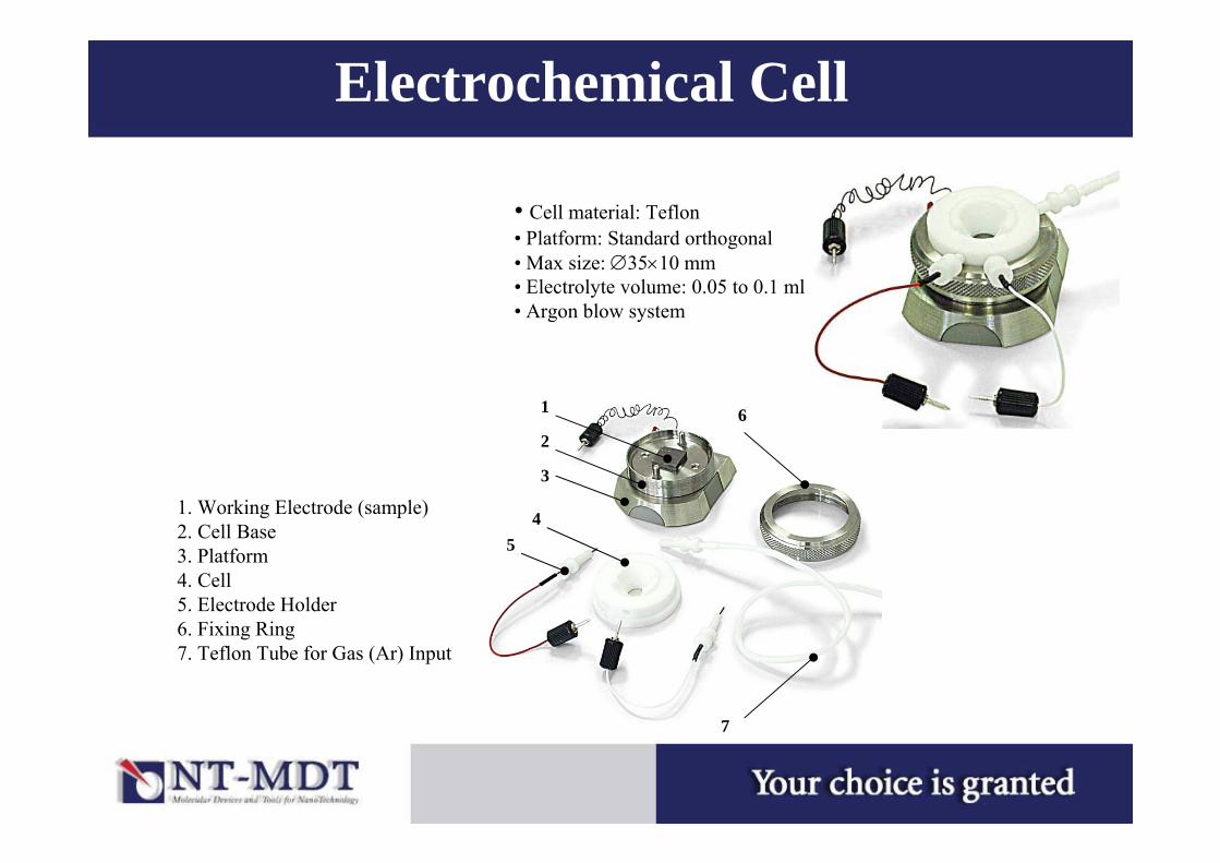
• Cell material: Teflon• Platform: Standard orthogonal• Max size: ∅35×10 mm• Electrolyte volume: 0.05 to 0.1 ml• Argon blow system
1. Working Electrode (sample)2. Cell Base3. Platform4. Cell5. Electrode Holder6. Fixing Ring7. Teflon Tube for Gas (Ar) Input
Electrochemical Cell
1
5
2
4
6
3
7

Bipotentiostat • Output Compliance Voltage: ± 15 V• Applied Voltage Range: ± 5 V (stability ± 1 mV)• Current Ranges: ± 5mA; ± 100 μA; ± 2 μA (accuracy of measurement ±0.1 % of the range)
• Reference Input Impedance: > 1011 ΩSoftware• Modes: manual; sweep (1 mV/s to 100 mV/s), pulse (time resolution 10 ms); potentiostatic currenttransients; cyclic and linear voltammetry; universalprogrammer
• Computer: Pentium II or higher• System: Windows 98/XP
Bipotentiostat & Software

Working:∅ 4-15 mm (Au 111),Pt (111), HOPG, polishedpolycrystalline metals)
Counter: Cu, Pt, Au-wire
Reference: Cu, Pt, Au-wire,Ag/AgCl (Cypress system)
Electrolyte: H2SO4 (50mM) + CuSO4 (1mM)or any suitable electrolyte
Working Electrode: monocrystal Au (111)
Working Electrode: monocrystal Pt (111)
Working Electrode: HOPG (0001)
Reference Electrode: Ag/AgCl (Cypress System)
Electrodes

• Material: W, Pt-Ir (10-25%)• Size: ∅ 0.4-0.5 mm,
max length 20 mm (insulated part 5-7 mm)
• Sharpening: electrochemical, mechanical
• Insulation: “Apiezon Wax”,polyethylene
Technological Scheme of Tip Insulation Process
STM Electrochemical Tips
Probe Spectroscopy
Results
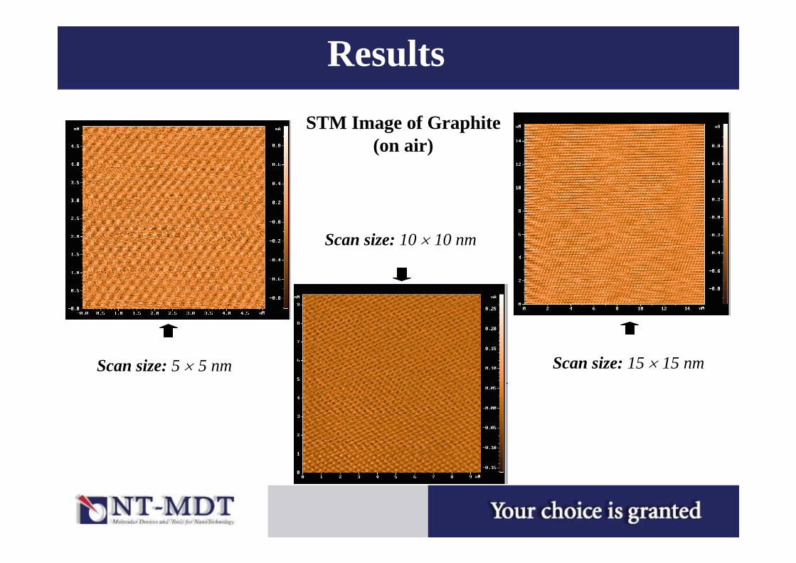
Scan size: 5 × 5 nm
Scan size: 10 × 10 nm
STM Image of Graphite(on air)
Scan size: 15 × 15 nm

Results
Scan size: 0.8 × 1.1 µmGraphite surface decoration by copper clusters during dynamic electro deposition process
Scan size: 4.1x4.1 nmAtomic resolution of HOPG in Electrolyte solution(0.05 M H2SO4 + 1 mM CuSO4) under potential.
STM Image of Graphite (in solution)
t

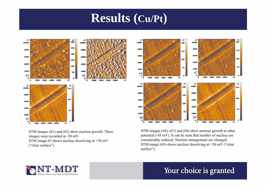
Results (Cu/Pt)A piece of Cu wire was used as the quasi reference electrode and counter electrode. Tungsten tips, which were etched in 2M KOH and subsequently coated with “Apiezon Wax” were used as tunneling probes. The Faradaic background current through the tip was below 10 nA.The Pt poly crystal was 3 mm in diameter. Prior to each experiment,the Pt electrode was flame annealed in flame for a few minutes.The electrolyte was 50 mM H2SO4 containing 1 mM CuSO4. Periodically the electrolyte was changed at the upper and lower potential limits. After this procedure the voltammetric response of the electrode was in reasonable agreement with the commonly accepted voltammogram of the Pt in 50 mM H2SO4.Applied potentials and numbers of STM images are presented in figures below.STM images are shown on next slide.
Cyclic voltammogram of the Pt electrode
Results (Cu/Pt)
STM images (64), (67) and (68) show nucleus growth at other potential (-45 mV). It can be seen that number of nucleus are considerably reduced. Nucleus arrangement are changed.STM image (69) shows nucleus dissolving at +30 mV (“clear surface”).
STM images (61) and (62) show nucleus growth. These images were recorded at -50 mV.STM image 63 shows nucleus dissolving at +30 mV (“clear surface”).

Results (Cu/Au)A piece of Cu wire was used as the quasi reference electrode and counter electrode. Tungsten tips, which were etched in 2M KOH and subsequently coated with “Apiezon Wax” were used as tunneling probes. The Faradaic background current through the tip was below 10 nA. The Au monocrystal was 10 mm in diameter. Prior to each experiment, the Au electrode was flame annealed in flame for a few minutes.The electrolyte was 50 mM H2SO4 containing 1 mM CuSO4. Periodically the electrolyte was changed at the upper and lower potential limits. After this procedure the voltammetric response of the electrode was in reasonable agreement with the commonly accepted voltammogram of the Au in 50 mM H2SO4.Applied potentials and numbers of STM images are presented in figures below. STM images are shown on next slides.Cyclic voltammogram of the Au electrode

Results (Cu/Au)
STM Images (51)-(54) show Cu dissolving. There are fair amount small nucleus. Their size is 0.2-0.4 μm.
STM Images (56)-(58) show Cu monocrystals growth. It can be seen facets of Cu (111) monocrystal. There are growth steps on big crystals.

Results (Cu/Au)
Scan size 20 × 20 nm
Scan size 3.5 × 3.5 nm
3D
Scan size 70 × 70 nm
Fig. 1. Au monatomic steps and islands resulting after flame annealing of Au substrate.Fig. 2, 3, 4. Lateral atomic resolution of co-adsorption lattice (√3х√3)R30° of Cu-ad atoms and bisulphate anions.
Scan size 30 × 30 nm
1
2
3
4
Scan size 70 × 70 nm
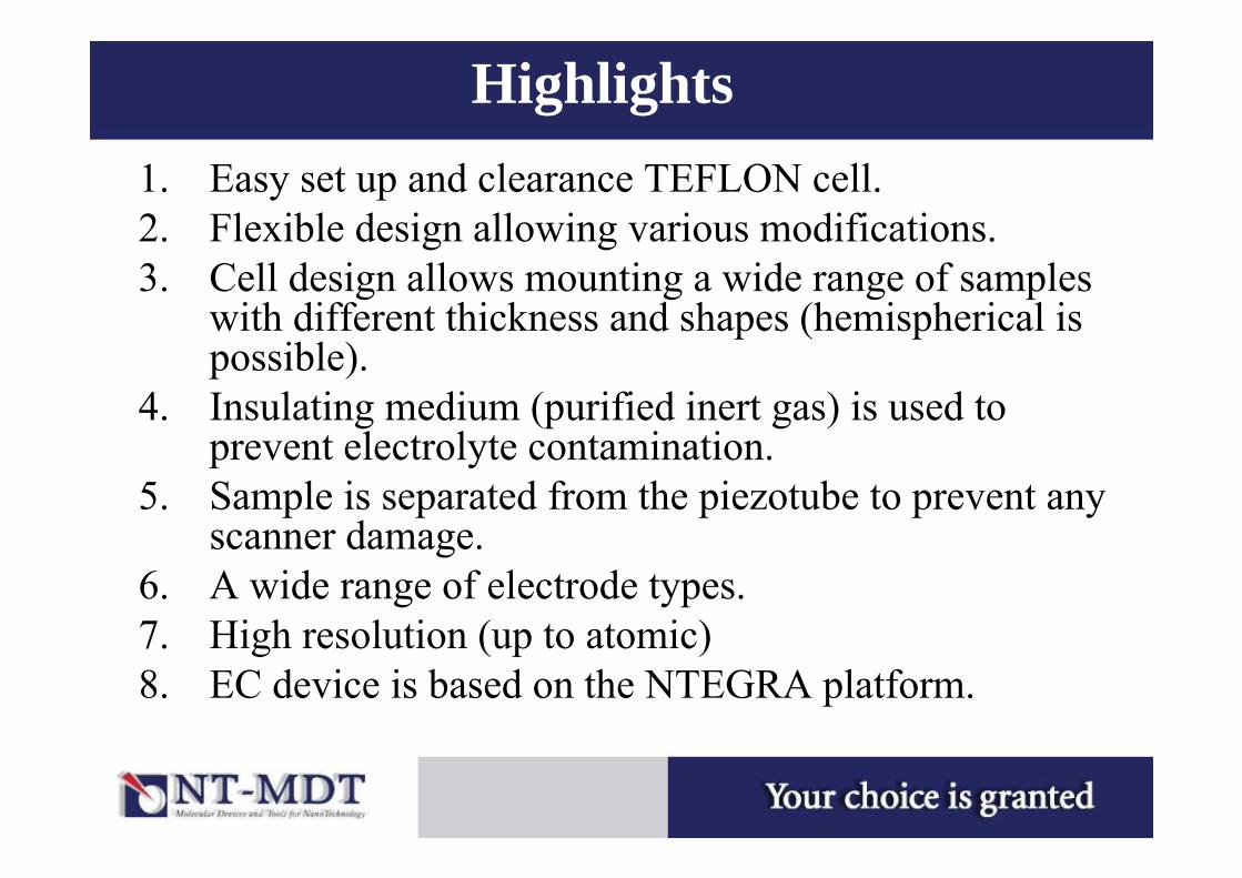
1. Easy set up and clearance TEFLON cell.2. Flexible design allowing various modifications.3. Cell design allows mounting a wide range of samples
with different thickness and shapes (hemispherical is possible).
4. Insulating medium (purified inert gas) is used to prevent electrolyte contamination.
5. Sample is separated from the piezotube to prevent any scanner damage.
6. A wide range of electrode types. 7. High resolution (up to atomic) 8. EC device is based on the NTEGRA platform.
Highlights
