novel applications in ion microbeam analysis alz simon a - libra
TRANSCRIPT

Novel applications in ion microbeam analysis
Alíz Simon
Institute of Nuclear Research of the Hungarian Academy of Sciences
(HAS-ATOMKI)
Debrecen, Hungary
LIBRA Meeting, 09/11/09 Athens, Greece

Motivation
A nuclear microprobe opens up new research areasat Demokritos Institute
Working Document onTHE RESEARCH INFRASTRUCTURES IN FP7
“…best research infrastructures existing in Europe..”“…forefront of the advancement of research..”
“Centre of excellence…”“Knowledge generation and, by implication, innovation…”
“…help industry … knowledge and technological know how”
What is your VISION?

Introduction • HAS-ATOMKI Accelerator Centre /Ion Beam Laboratory• Overview of the nuclear microprobe techniques
Research with microbeams in HAS-ATOMKI• Environmental research• Biomedical applications• Archaeology• Materials science• Modification of materials
Nuclear microprobe laboratories around the world
Outline

Institute of Nuclear Research of the Hungarian Academy of Sciences
ATOMKI
• Staff: 198• Main research fields:
– Theoretical nuclear physics– Atomic physics– Materials science– Earth science– Environmental research– Nuclear techniques
• Associated member of the University of Debrecen
HAS-ATOMKI

• 5MV Van de Graaff accelerator1H+, 2H+, He+, C+, N+ N2
+
Mainly used for IBA, Nuclear Physics & Astrophysics
• 100-1000kV Van de Graaff accelerator1H+, 2H+, 4He+, (C+)used for investigation of atomic collisions
• ECR Ion SourceElectromagnetic wave frequency 14.5 GHz, Extraction (acceleration) voltage 2...30 kV; mainly used for plasma diagnostics and investigation of ion-surface interactions
• K=20MeV Compact Cyclotron1H+, 2H+, 3He2+, 4He2+
Mainly used for isotopeproduction for medical applications & Nuclear Physics
Accelerator Centre

Section of Ion Beam Physics
Ion Beam Analysis Group
Beam lines on 5MV VdGMillibeam lines:
Aerosol science (PIXE)Nuclear Physics & AstrophysicsElectron spectrometer
Nuclear microprobe (1995)RBS, PIXE, PIGE, DIGE, IBIC, STIM, PBM
Nuclear AstrophysicsGroup
Dr. Fülöp, Dr. Gyürky

What is a nuclear microprobe?
General purpose, multidisciplinary instrument,
where high energy (MeV) ions are focussed down
to a micron size beam and scanned over the sample
for getting spectroscopic and imaging data.
Definition

transmitted ionsthrough thinsamples (STIM),(transmissionchannelling)
+ − + − + −− + − + − +
nuclearreactionproducts (NRA)
backscatteredions (RBS)
electrons
X-rays(PIXE)
Electrons and holesin semiconductorsor insulators (IBIC)
MeVion
beam
UV, visible, IR. IonBeam InducedLuminescence (IBIL)
Transmitted ionsthroughthin samples
(STIM,Transmission Channelling)
(SEM)
Ion-solid interactions

• Oxford Microbeams Ltd.• Built on the 0o beamline of the
5 MV Van de Graaff accelerator • Beams: H+, D+, 4He+
• Energy range: 0.6-3.5 MeV• Beam size: 1 μm x 1 μm• IBA techniques: PIXE, PIGE, DIGE,
RBS, STIM, IBIC• Applications: archaeology, geology,
biology, environmental science materials science, modification of materials, PBM
Debrecen Scanning Nuclear Microprobe

Imaging of elemental distribution on micro-scaleElemental maps of minute samples as for e.g. minerals, biological cells,aerosol particles, etc.
Micro-characterisation Determination of elemental concentrations in micro-particles, composition and thicknesses of thin metallic films, etc.
Micro-charge deposition (Ion Beam Induced Current -IBIC, single event upset)
Micro-irradiation (e.g. single cell irradiation),
Micro-damage (testing reliability of electronic devices),
Micro-machining (producing miniature devices), etc.
Applications of a Nuclear Microprobe

“Traditional” techniques (~pA): PIXE, RBS, NRA, PIGE
Low-current techniques (~fA): IBIC, IBIL, STIM
Spectra
Data acquisition
Imaging
Elemental maps
Tomographic images
Pulse height maps
LISTMODE
Analytical techniques

M. Takai, et al., Nucl. Instr. and Meth. in Phys. Res. B 64 (1992) 277.
Schematic diagram of data block for RBS mapping and tomography

HAS-ATOMKI LOGO
Courtesy to I. Rajta& M. Novak, HAS-ATOMKI
The beam is scanned on a quartz. The subsequent images are integrated.
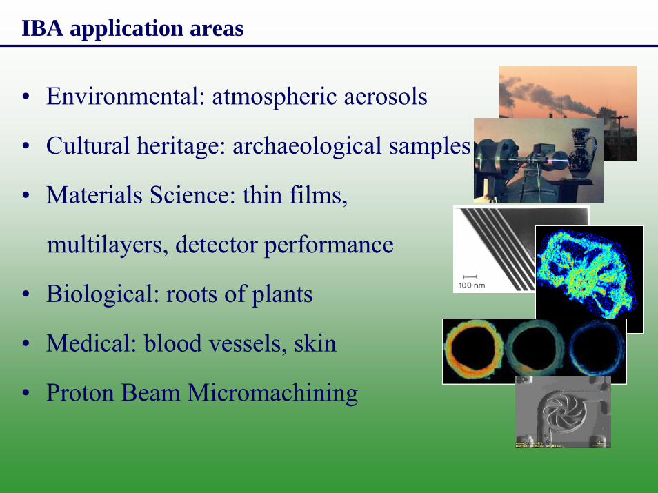
IBA application areas
• Environmental: atmospheric aerosols
• Cultural heritage: archaeological samples
• Materials Science: thin films,
multilayers, detector performance
• Biological: roots of plants
• Medical: blood vessels, skin
• Proton Beam Micromachining

Environmental-Atmospheric aerosols
• Urban and rural aerosol in Eastern Hungary
• EU regulation• Origin of aerosols• Stochastic lung models
(deposition of different sized aerosol particles in healthy and diseased bronchial )
Rural sampling site for background values in Hortobágy

The health effects of the inhaled particles may strongly depend on the
location of deposition within the lung.
SiAl Ca Fe
ClK NaN Mg
TiZnO P
SIndividual aerosol particles
50 μm
Environmental- Individual aerosols μPIXE, STIM, μRBS

Environment- Metal uptake of plants
Cl Ca
Fe
Mg
SP
Cr
Si
Na
K
MnTi
C O
Ni
Al
ClCl CaCa
FeFe
MgMg
SSPP
CrCr
SiSi
NaNa
KK
MnMnTiTi
CC OO
NiNi
AlAl
Identified tissues:• Rhisodermis• Parenchyma• Vascular cilinder
The uptake of toxic element is associated with the presence of iron plaques.
These elements remain trapped in the root.
These plants can be used for monitoring.
μPIXE, STIM

Biomedical applications
Cross sectional distribution of Ca
concentration.
high
low
Study of calcification process in carotis
Number of concatenated bitmaps: 21.∅ ~ 7 mm.
μPIXE, STIM, μRBS
True mapsTrue maps 0 60000 0 20000 0 20000 0 60000
Cl P S TiSTIM + Ti
TiO2 nanoparticle penetration in the epidermis of human skin xenografts

Complex investigation of fish otoliths μPIXE, μRBS, μERDA
0-70 nm
70-140 nm
140-210 nm
H maps by micro-ERDA Ca maps analysed by micro-RBS

Cultural Heritage
Analysis of classical ring-stones from the17-18th century and their imitations
Characterisation of Dyrrhachium silver coinsfrom 68-43 years BC → degradation of the of Ag content→ chronological classification
Investigation of prehistoric incrusted pottery
Ca P Si
100 μm
min
maxCa P Si
100 μm
min
maxCa P SiCa P Si
100 μm
min
max
Max
Min
Max
Min
C N O
100 μm
Max
Min
Max
Min
C N O
100 μm
Ca P Si
100 μm
min
maxCa P Si
100 μm
min
maxCa P SiCa P Si
100 μm
min
max
Max
Min
Max
Min
C N O
100 μm
Max
Min
Max
Min
C N O
100 μm
Ornamentingwhite substancedoes contain bone grit?
μPIXE, μPIGE, μRBS

A. Simon et al. NIMB 249 (2006) 454.
Materials Science-Thin (nm) Film Analysis
Deposit size: approx. 3 cm x 4cmPlease note the non-uniform film
thickness
Boron carbide, B4C• Micro-drives used in consumer
electronics require an increased areal storage density.
• Hard disk industry is aiming at 1Tbit/inch2.• Protective overcoat for the head and the
disk requires smooth, wear resistant, pinhole-free, thermally stable
material for wear and corrosion protection at 1nm
thickness.• Currently used CNx ⇒ B4C
( and/or SiN
μRBS
High lateral resolution mapping of the B/C ratio in a boron carbide film formed by femtosecond pulsed laser deposition
x ,BxCyNz)

Thickness distribution by spectroscopic ellipsometry
-16 -12 -8 -4 0 4 8 12 160
20
40
60
80
Tota
l film
thic
knes
s (μ
g/cm
2 )
Position (mm)
X-line Y-line
The results of the RBS analyses:• the film thickness is not uniform; • it has a maximum in the centre: d=71 μg/cm2 (3736x1015at/cm2); • a steep decrease is observed toward to the edges;• minimum film thickness of d~9 μg/cm2 (484x1015 at/cm2).
Thickness distribution by RBS microbeam (2.5 MeV He+)
Layer thickness distribution μRBS

-16 -12 -8 -4 0 4 8 12 160
10
20
30
40
50
60
Ele
men
tal f
ilm th
ickn
ess
(μg/
cm2 )
Y position (mm)
oxygen carbon boron
• The elemental composition is indeed highlynon-uniform.
• The B/C ratio has a maximum at the centrewith elemental contents of
boron: 50±5 μg/cm2) ;oxygen:8±3 μg/cm2; carbon: 16±2 μg/cm2.
• The B/C~1 ratio measured at the edge of thedeposit increases up to about 3 toward the centre (the target composition was B4C).
Lateral elemental profiles of the boron carbide layer
Similar investigations of target uniformity with the Nuclear AstrophysicsGroup in order to increase the precision of their measurements.Kiss G. Gy. 1 + , Rauscher T. 4 , Gyürky Gy. 1 + , Simon A. 1 + , Fülöp Zs. 1 + , Somorjai E. 1 + : Coulomb suppression of the stellar enhancement factor. Physical Review Letters 101 (2008)19:1101(4)/
Rauscher T. 4 , Kiss G. Gy. 1 + , Gyürky Gy. 1 + , Simon A. 1 + , Fülöp Zs. 1 + , Somorjai E. 1 + : Suppression of the stellar enchancement factor and the reaction 85Rb(p,n)85Sr. , Physical Review C 80 (2009)3:5801(12)
Yalcin C. 2 + 2 , Güray R. T. 4 , Özkan N. 4 , Kutlu S. 4 , Gyürky Gy. 1 + , Farkas J. 1 + , Kiss G. Gy. 1 + , Fülöp Zs. 1 + , Simon A. 1 + , Somorjai E. 1 + , Rauscher T. 4 : Odd p isotope 113In: Measurement of alpha-induced reactions. Physical Review C 79 (2009)5801(9)/
μRBS

Proton Beam Micromachining
• Focused MeV energy ion beam is scanned over a suitable resist material and subsequently chemically developed
• Advantages of PBM:– Direct write 3D lithography method– Short irradiation time– Good depth of field: nearly 90° walls– Well defined depth due to ion ranges: buried microchannels
• Post lithography step: electroplating– Metal micro-molds and stamps
Microreactors, Micro-electrochemical cell, Microfluidic-reactor, micro-optical devices, Silicon: micro- turbine, pump, filters for medical research, etc.

Top: 8 µm wide and 50 µm lattice constant two-dimensionalBottom:15 µm wide 30 µm lattice constant one-dimensional grating
and their diffraction images
Top: 8 µm wide and 50 µm lattice constant two-dimensionalBottom:15 µm wide 30 µm lattice constant one-dimensional grating
and their diffraction images
R. Huszank et al., Fabrication of optical devicesin poly(dimethylsiloxane) by proton microbeam,Opt. Commun. (2009), doi:10.1016/j.optcom.2009.09.066
PBM-Diffraction gratings Modification

Top: Fresnel zone plate,130 mm focal length with 2000 µm diameter convergent typeBottom: diffraction images (left) at the focal point and (right) at 420 mm from the zone
plate.
Top: Fresnel zone plate,130 mm focal length with 2000 µm diameter convergent typeBottom: diffraction images (left) at the focal point and (right) at 420 mm from the zone
plate.
R. Huszank et al., Fabrication of optical devices in poly(dimethylsiloxane) by proton microbeam, Opt. Commun. (2009), doi:10.1016/j.optcom.2009.09.066
PBM-Fresnel zone plate Modification

SEM Back-scattered electrons
IBIC map
IBIC Microscopy Imaging of CVD Diamond IBIC
• Investigating radiation sensor performance
• Uniformity of charge collection efficiency
• Imaging intra-crystallite charge transport
• Correlating CCE with
morphology electric field temperature
A. Simon et al. NIMB 219-20 (2004) 1022.

Pulse height spectra of selected regions within the crystallite
020406080
100120140160180
0 10 20 30 40 50 60 70 80 90 100
Charge collection efficiency (%)
Cou
nts
B C
A
ElectrodeElectrode
ElectrodeElectrode

900 1000 1100 1200 1300 14000
20
40
60
80
100
120
140
160
180
200
220
Cou
nts /
Cha
nnel
Energy (keV)
109 ion/cm2
1010 ion/cm2 5x10¹⁰ ion/cm2 5x10¹¹ ion/cm2
Hamamatsu S5821PIN photodiode
1.2 mm
U d = 0 VU d = 0 VIBIC map: 0V bias left. The full irradiated area (340x340 μm2) is shown including the individually irradiated 100x100 μm2 squares by fluences from bottom to top and right to left: 0.01, 0.02, 0.05, 0.1, 0.2, 0.5, 1, 2 and 5x10¹¹ ion/cm2, respectively.
Si PIN photodiode IBIC

CERN-RD50 collaborations
http://rd50.web.cern.ch/RD50/

SPIRIT http://www.spirit-ion.eu/
Support of Public and Industrial Research using Ion beam Technology
SPIRIT represents an Integrated InfrastructureInitiative (I3) funded by the European Commission. The SPIRIT consortiumintegrates leading european ion beam facilitiesand R&D providers, which provide ions in an energy range from ~10 keV to 100 MeV forthe modification and analysis of solid surfaces,interfaces, thin films and nanostructured systems. The main application areas are materials, biomedical and environmental research and technology.
SPIRIT integrates 11 leading ion beam facilities from 6 European Member States and 2 Associated States.7 partners provide TransNational Access.

TNA Services offered by SPIRIT http://www.spirit-ion.eu/
FZD (coordinator of SPIRIT) Forschungszentrum Dresden-Rossendorf , CNRS Centre National de la Recherche Scientifique, Bordeaux, KUL Katholieke Universiteit Leuven , JSI Jozef Stefan Institute, Ljubljana, UBW Universität der Bundeswehr München, CEA Commissariat à L’Energie AtomiqueSUR University of Surrey, Guildford

CHARISMA-FP7 I3 project 2009-2013
Coordinator:Prof. Bruno G. BrunettiUNIVERSITA DEGLI STUDI DI PERUGIA, ItalyDipartimento di Chimica, Centro SMAArt
21 participants : museums, research institutes, universitiesProject started: 1st October, 2009, TNA available from 1st January, 2010
FOUNDATION FOR RESEARCH AND TECHNOLOGY - HELLAS Institute of Electronic Structure and Laser, Demetrios AnglosIDRYMA "ORMYLIA, Art Diagnosis Centre, Hieromonk Serapion Simonopetritis
HAS- ATOMKI, For TNA service contact: Aliz Simon, [email protected]
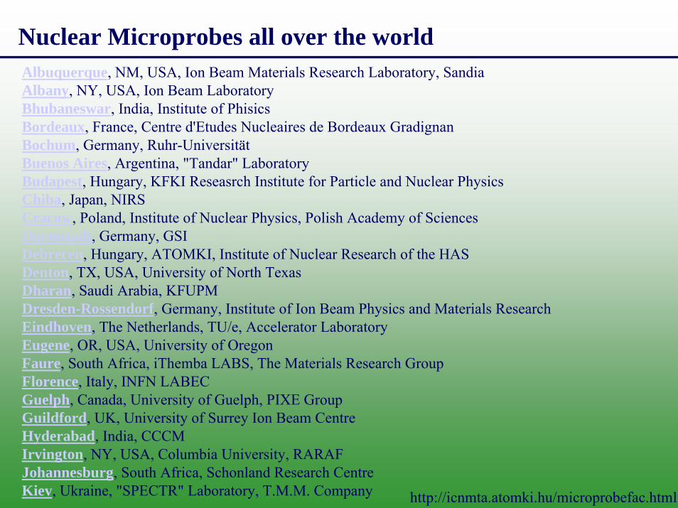
Albuquerque, NM, USA, Ion Beam Materials Research Laboratory, SandiaAlbany, NY, USA, Ion Beam LaboratoryBhubaneswar, India, Institute of PhisicsBordeaux, France, Centre d'Etudes Nucleaires de Bordeaux GradignanBochum, Germany, Ruhr-UniversitätBuenos Aires, Argentina, "Tandar" LaboratoryBudapest, Hungary, KFKI Reseasrch Institute for Particle and Nuclear PhysicsChiba, Japan, NIRSCracow, Poland, Institute of Nuclear Physics, Polish Academy of SciencesDarmstadt, Germany, GSIDebrecen, Hungary, ATOMKI, Institute of Nuclear Research of the HASDenton, TX, USA, University of North TexasDharan, Saudi Arabia, KFUPMDresden-Rossendorf, Germany, Institute of Ion Beam Physics and Materials ResearchEindhoven, The Netherlands, TU/e, Accelerator LaboratoryEugene, OR, USA, University of OregonFaure, South Africa, iThemba LABS, The Materials Research GroupFlorence, Italy, INFN LABECGuelph, Canada, University of Guelph, PIXE GroupGuildford, UK, University of Surrey Ion Beam CentreHyderabad, India, CCCMIrvington, NY, USA, Columbia University, RARAFJohannesburg, South Africa, Schonland Research CentreKiev, Ukraine, "SPECTR" Laboratory, T.M.M. Company
Nuclear Microprobes all over the world
http://icnmta.atomki.hu/microprobefac.html

Lafayette, LA, USA, Louisiana Accelerator Center, Univ. of LouisianaLegnaro (Padova), Italy, INFN LNLLeipzig, Germany, LIPSIONLisbon, Portugal, ITN, Sacavem, Ion Beam LaboratoryLivermore CA, USA, LLNL, CAMSLjubljana, Slovenia, Jozef Stefan Institute, Microanalytical CenterLos Alamos, NM, USA, LANL, Ion Beam Materials LaboratoryLower Hutt, New Zealand, Nuclear Microprobe at GNSMenai, Australia, ANSTOLund, Sweden, Lund University, Nuclear PhysicsMadrid, Spain, CMAMMelbourne, Australia, MARCMelbourne, Australia, CSIRO-GEMOC Nuclear MicroprobeMünchen, Germany, Technische UniversitätParis, France, Lab. de Rech. des Musees (Louvre)Saclay, France, Lab. Pierre Sue CEA/CNRSSevilla, Spain, Centro National de AceleradoresShanghai, China, Institute of Modern Physics, Fudan UniversityShanghai, China, Shanghai Nuclear InstituteSendai, Japan, Tohoku UniversitySingapore, Centre for Ion Beam Applications, National University of SingaporeTakasaki, Gunma, Japan, TIARA at JAERITeheran, Iran, Nuclear Research Centre, AEOIZagreb, Croatia, Rudjer Boskovic Institute
Nuclear Microprobes all over the world
http://icnmta.atomki.hu/microprobefac.html

Contributions are acknowledged to
HAS-ATOMKI
Z. ElekesR. HuszankZs. KertészÁ.Z. KissI. RajtaG. SzikiZ. SzikszaiSz. SzilasiI. Uzonyi
University of SurreyC. JeynesP. SellinA.Lohstroh
University of SzegedT. SzörényiT. Csákó
The financial support from the LIBRA project and CHARISMA project No. 228330 is acknowledged.