notes on npn transistors - university of california, san diego on npn... · notes on npn...
TRANSCRIPT
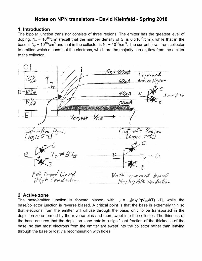
Notes on NPN transistors - David Kleinfeld - Spring 2018 1. Introduction The bipolar junction transistor consists of three regions. The emitter has the greatest level of doping, Nn ~ 1018/cm3 (recall that the number density of Si is 6 x10²¹/cm3), while that in the base is Np ~ 1016/cm3 and that in the collector is Nn ~ 1015/cm3. The current flows from collector to emitter, which means that the electrons, which are the majority carrier, flow from the emitter to the collector.
2. Active zone The base/emitter junction is forward biased, with IC = Io[exp(qVBE/kT) -1], while the base/collector junction is reverse biased. A critical point is that the base is extremely thin so that electrons from the emitter will diffuse through the base, only to be transported in the depletion zone formed by the reverse bias and then swept into the collector. The thinness of the base ensures that the depletion zone entails a significant fraction of the thickness of the base, so that most electrons from the emitter are swept into the collector rather than leaving through the base or lost via recombination with holes.
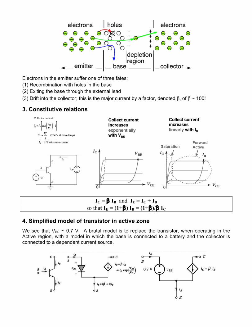
Electrons in the emitter suffer one of three fates: (1) Recombination with holes in the base (2) Exiting the base through the external lead (3) Drift into the collector; this is the major current by a factor, denoted β, of β ~ 100!
3. Constitutive relations
IC = β IB and IE = IC + IB so that IE = (1+β) IB = (1+β)/β IC
4. Simplified model of transistor in active zone We see that VBE ~ 0.7 V. A brutal model is to replace the transistor, when operating in the Active region, with a model in which the base is connected to a battery and the collector is connected to a dependent current source.
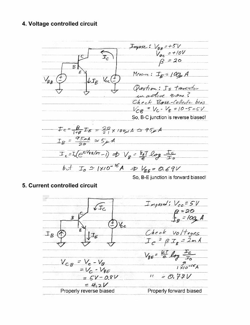
4. Voltage controlled circuit
5. Current controlled circuit
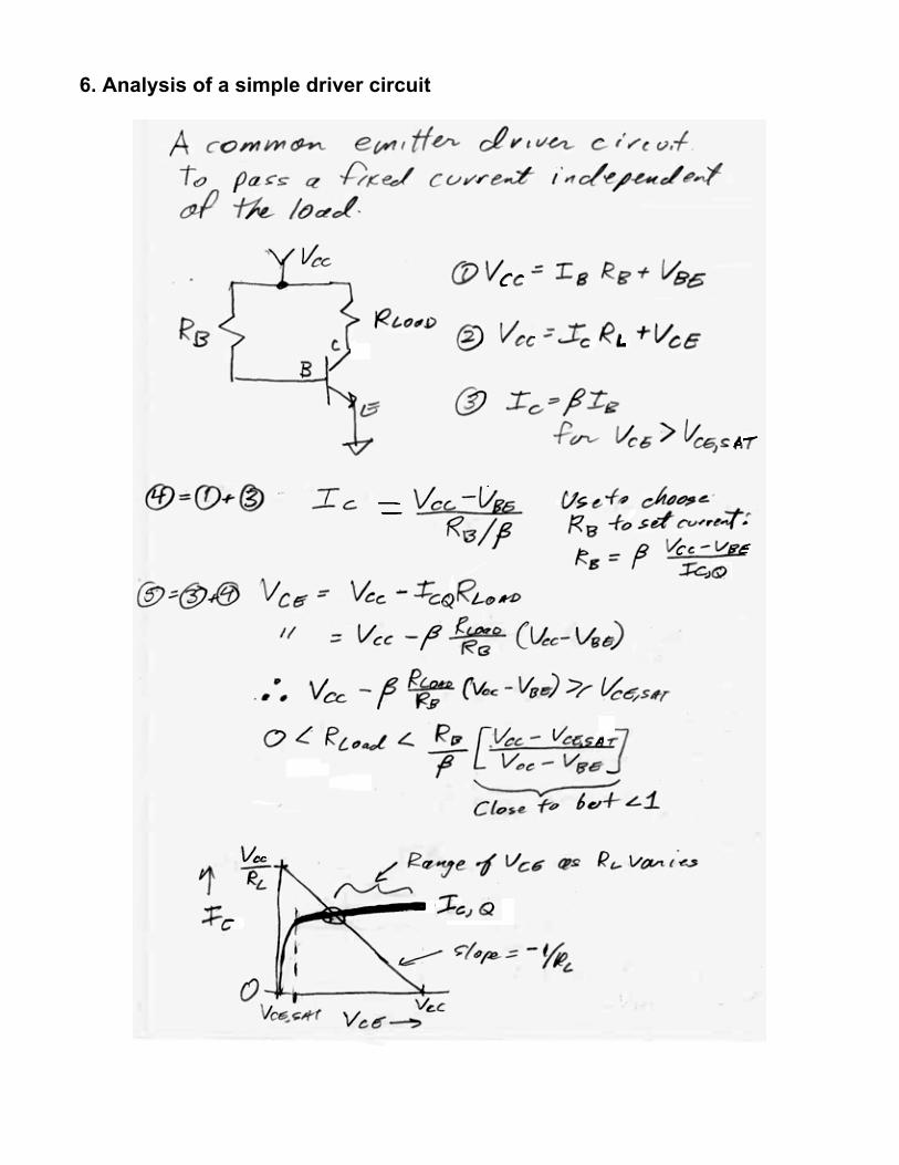
6. Analysis of a simple driver circuit
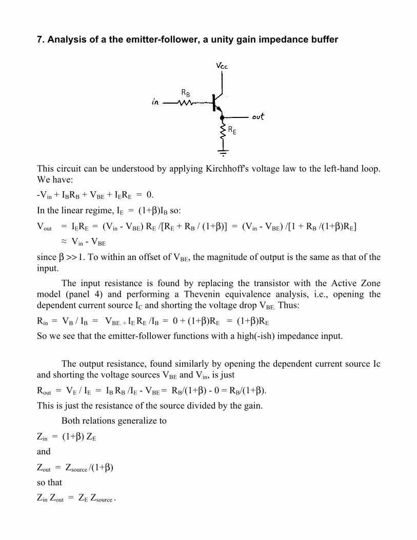
7. Analysis of a the emitter-follower, a unity gain impedance buffer
This circuit can be understood by applying Kirchhoff's voltage law to the left-hand loop. We have: -Vin + IBRB + VBE + IERE = 0.
In the linear regime, IE = (1+β)IB so:
Vout = IERE = (Vin - VBE) RE /[RE + RB / (1+β)] = (Vin - VBE) /[1 + RB /(1+β)RE] ≈ Vin - VBE
since β >> 1. To within an offset of VBE, the magnitude of output is the same as that of the input. The input resistance is found by replacing the transistor with the Active Zone model (panel 4) and performing a Thevenin equivalence analysis, i.e., opening the dependent current source IC and shorting the voltage drop VBE. Thus:
Rin = VB / IB = VBE. + IE RE /IB = 0 + (1+β)RE = (1+β)RE So we see that the emitter-follower functions with a high(-ish) impedance input.
The output resistance, found similarly by opening the dependent current source Ic and shorting the voltage sources VBE and Vin, is just
Rout = VE / IE = IB RB /IE - VBE = RB/(1+β) - 0 = RB/(1+β). This is just the resistance of the source divided by the gain. Both relations generalize to
Zin = (1+β) ZE and
Zout = Zsource /(1+β) so that Zin Zout = ZE Zsource .