noise modeling at quantum level for multi-stack gate dielectric mosfets
DESCRIPTION
Noise Modeling at Quantum Level for Multi-Stack Gate Dielectric MOSFETs. Zeynep Çelik-Butler Industrial Liaisons: Ajit Shanware, Luigi Colombo, Keith Green, TI; Hsing-Huang Tseng, SEMATECH, Ania Zlotnicka, Freescale Students: Bigang Min, Siva Prasad Devireddy, Tanvir Morshed, Shahriar Rahman - PowerPoint PPT PresentationTRANSCRIPT

UTA Noise and Reliability Laboratory 1
Noise Modeling at Quantum Level for Multi-Stack Gate Dielectric MOSFETs.
Zeynep Çelik-Butler
Industrial Liaisons: Ajit Shanware, Luigi Colombo, Keith Green, TI; Hsing-Huang Tseng, SEMATECH,
Ania Zlotnicka, Freescale
Students:Bigang Min, Siva Prasad Devireddy, Tanvir
Morshed, Shahriar RahmanUniversity of Texas at Arlington
P. O. BOX 19072Arlington, TX 76019

UTA Noise and Reliability Laboratory 2
Outline
Noise Modeling Unified Flicker Noise Model Multi-Stack Unified Noise Model (MSUN)
Experimental Verification Metal-Gated HfO2/SiO2 NMOSFETs – different interfacial layer processing Poly-Gated HfSiON/SiON NMOSFETs – variable interfacial layer thickness
Conclusions and Future Work

UTA Noise and Reliability Laboratory 3
Unified Flicker Noise Model*
Based on correlated number and mobility fluctuations theory.
Equi-energy tunneling process. Traps in the gate dielectric trap/de-trap channel carriers Trapping/de-trapping phenomenon causes fluctuations in
the carrier number. Fluctuations in carrier mobility due to remote Coulomb
scattering from trapped charge. Uniform distribution of traps in the gate dielectric with
respect to distance and energy level.
*K. K. Hung, P. K. Ko, C. Hu, Y. C. Cheng, “A unified model for the flicker noise in metal-oxide-semiconductor field-effect transistors,” IEEE Trans. Electron Devices, vol. 37, pp.654-665, 1990.
UTA Noise and Reliability Laboratory 4
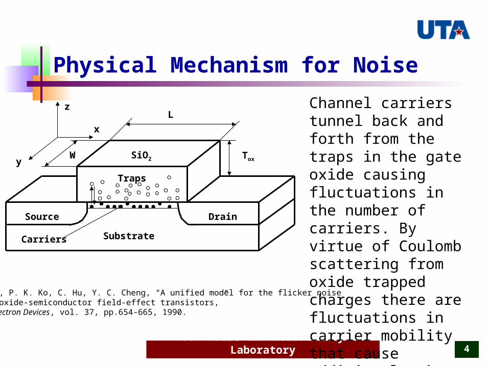
Physical Mechanism for Noise
Channel carriers tunnel back and forth from the traps in the gate oxide causing fluctuations in the number of carriers. By virtue of Coulomb scattering from oxide trapped charges there are fluctuations in carrier mobility that cause additional noise in correlation with the carrier number fluctuations.
Lz
x
yW SiO2 Tox
Source Drain
Substrate
Traps
Carriers
K. K. Hung, P. K. Ko, C. Hu, Y. C. Cheng, “A unified model for the flicker noise in metal-oxide-semiconductor field-effect transistors,” IEEE Trans. Electron Devices, vol. 37, pp.654-665, 1990.

UTA Noise and Reliability Laboratory 5
Unified Flicker Noise Model Expressions
mh
24
K. K. Hung, P. K. Ko, C. Hu, and Y. C. Cheng IEEE Trans. Electron Devices, vol. 37, pp.654-665,1990 teffsc
dI
NNfWL
kTIS
d
22
)1
(
)exp(0 z
2*
2
2
2
22
00*
*0
2
2
..
2log
NN
NNOICNNOIBNOIA
LWf
LkTI
NNNOIC
NNNOIBNN
NNNOIA
LfC
IkTqS
L
LL
effEF
clmd
LLL
effEF
ox
effd
Id
BSIM Low Frequency Noise Model

UTA Noise and Reliability Laboratory 6
High-k Gate Stack Scenario
Lz
x
yW High-k
THK
TIL
Source Drain
Substrate Interfacial layer
Traps x
Carriers
y z
Channel carriers tunnel into the traps in high-k and interfacial layer causing fluctuations in carrier number and mobility in a correlated way.
The different trap profiles and various physical properties of high-k/interfacial layer materials like physical thicknesses, barrier heights etc. affect the 1/f noise.
The uniform dielectric trap density assumption does not hold.

UTA Noise and Reliability Laboratory 7
Multi-Stack Unified Noise Model (MSUN)
Based on correlated number and mobility fluctuations theory Equi-energy tunneling process Traps in the gate dielectric layers trap/de-trap channel carriers Trapping/de-trapping phenomenon causes fluctuations in the
carrier number Fluctuations in carrier mobility due to remote Coulomb
scattering from trapped charge Scalable with regards to the high-k/interfacial layer physical
thicknesses Takes different dielectric material properties into account Considers non-uniform distribution of traps in the
high-k/interfacial layer with respect to distance and energy level

UTA Noise and Reliability Laboratory 8
Typical Band Diagram for High-k Stack
Carrier tunneling probability into the gate dielectric is an exponentially decaying function with attenuation rates corresponding to the dielectric material.
NtIL0 – IL/Si interface trap density at intrinsic Fermi level
NtHK0 – HK/IL interface trap density at intrinsic Fermi level
THK
Ev
Efn
TIL
Ec
Ei
NtIL0
NtHK0
exp[-γHK(zTIL)]
exp(-γILz)
)exp()exp(0
zTTHKILHKILIL
)exp(0
zIL

UTA Noise and Reliability Laboratory 9
Trap Density Profile in SiO2
0 1.2Ei
Nt0
Nt0 exp(ξ(Efn-Ei))
0 z
Nt(Efn)
Nt(Efn) exp(ηz)
Z. Çelik-Butler, and T. Y. Hsiang, “Spectral dependence of 1/fγ noise on gate bias in n-MOSFETs,” Solid State Electron., vol. 30, pp. 419–423, 1987.
Nt0 is the trap density at the Si/SiO2 interface and intrinsic Fermi level. Trap density increases exponentially towards the band edges at a rate defined by parameter ξ.
Nt(Efn) is the trap density at the Si/SiO2
interface and quasi-Fermi level. Trap density increases exponentially into the gate dielectric.
Nt0 exp(ξ(Efn-Ei))=Nt(Efn)
])()(exp[),(0
zzTVqEENzENILILgILILifnILtILfntIL
])()(exp[),(0
zzTVqEENzENHKHKgHKHKifnHKtHKfntHK

UTA Noise and Reliability Laboratory 10
Modified Trap Profile by Energy Band Bending
The energy bands bend in both high-k and interfacial layers due to the applied gate voltage. Higher trap density towards the band edges means that the trap profile encountered by channel carriers at a particular location in the dielectric is altered due to band bending. This effect is reflected by the parameters λIL and λHK.
High-K
Ev
Ei
Interfacial Layer
Ec
Ef
NtIL0
NtHK0
])()(exp[),(0
zzTVqEENzENILILgILILifnILtILfntIL
])()(exp[),(0
zzTVqEENzENHKHKgHKHKifnHKtHKfntHK
Z. Çelik-Butler, and T. Y. Hsiang, “Spectral dependence of 1/fγ noise on gate bias in n-MOSFETs,” Solid State Electron., vol. 30, pp. 419–423, 1987.

UTA Noise and Reliability Laboratory 11
Trap Density in High-k Stack
])()(exp[),(0
zzTVqEENzENILILgILILifnILtILfntIL
])()(exp[),(0
zzTVqEENzENHKHKgHKHKifnHKtHKfntHK
Trap density for (0<z<TIL)
Trap density for (TIL<z<THK+TIL)
)exp(0
zIL
)exp()exp(0
zTTHKILHKILIL

UTA Noise and Reliability Laboratory 12
Total Noise
dEdydzzyxE
zyxEfxfzyxEN
dEdydzzyxE
zyxEfxfzyxENfxS
t
E
E
W TT
TtHKt
t
E
E
W T
ttILN
c
v
ILHK
IL
c
v
IL
t
),,,(1
),,,()1(),,,(4
),,,(1
),,,()1(),,,(4),(
220
220 0
Power spectral density of the mean square fluctuations in the number of occupied traps for high-k/interfacial layer stack
B. Min, S. P. Devireddy, Z. Çelik-Butler, A. Shanware, L. Colombo, K. Green, J. J. Chambers, M. R. Visokay, and A. L. P. Rotondaro, “Impact of interfacial layer on low-frequency noise of HfSiON dielectric MOSFETs,” IEEE Trans. Electron Devices, vol. 53, pp. 1459–1466, 2006.
Z. Çelik-Butler, “Different noise mechanisms in high-k dielectric gate stacks,” in Proc. SPIE—Noise and Fluctuations, pp. 177–184, 2005.

UTA Noise and Reliability Laboratory 13
MSUN Noise Model Simplification
ft(1-ft) ensures that only traps within few kT of Efn contribute to fluctuations.
Integral along the channel (x) approximated. The shape of the spectral density is modified from pure 1/f
through functional form of Nt. Contribution to fluctuations from the high-k dielectric layer is
much higher than that from the interfacial layer.

UTA Noise and Reliability Laboratory 14
MSUN Noise Model Expressions
xkTWX
duu
u
T
EEN
duu
uEEN
fxSILILHKHK
ILIL
HKHK
HKHK
ILIL ILIL
ILIL
t TT
TILHKILHK
ifnHKtHK
T
IL
ifnILtIL
N
4
1})exp{(
)](exp[
1
)](exp[
),()exp(
)exp(2
)(
)(
0
0
)exp(
2
)(
)(
0
0
0
0
0
0
After appropriate substitution of various parameters, the power spectral density of the mean square fluctuations can be written as
])([ILILgILILIL
TVq
])[(HKHKgHKHKHK
TVq HKHKHK
mh
24
ILILILm
h 2
4
Conduction Band Offset with Si
Tunneling Coefficients

UTA Noise and Reliability Laboratory 15
MSUN Model Expressions (con.)
xdxfxSL
fSL
II dd
02
),(1
)(
),())(
1(),(
2
fxSxNxW
IfxS
td Neffscd
I
Total noise power spectral density
Power spectral density for local current fluctuations

UTA Noise and Reliability Laboratory 16
Outline
Noise Modeling Unified Flicker Noise Model Multi-Stack Unified Noise Model (MSUN)
Experimental Verification Metal-Gated HfO2/SiO2 NMOSFETs – different interfacial layer processing Poly-Gated HfSiON/SiON NMOSFETs – variable interfacial layer thickness
Conclusions and Future Work

UTA Noise and Reliability Laboratory 17
Experimental Verification Split C-V and DC Measurements
• 10µm 10µm devices • 78K & 100K – 350K in steps of 25K (metal gate)• 172K – 300K (poly gate)
Noise and DC Measurements• Metal gate
• 0.165µm 10µm devices• 78K & 100K – 350K in steps of 25K
• Poly gate• (0.20-0.25)µm 10µm devices• 172K – 300K
Noise Modeling and Analysis• Unified Flicker Noise Model• Multi-Stack Unified Model

UTA Noise and Reliability Laboratory 18
Metal Gated HfO2/SiO2 MOSFETs
Gate Electrode
High-k IL Type IL Thickness
TaSiN27Å HfO2
(ALD)SRPO SiO2 10Å
TaSiN 27Å HfO2
(ALD)RCA SiO2 10Å

UTA Noise and Reliability Laboratory 19
Normalized Noise vs. Temperature
Normalized noise for the two process splits shows no clear dependence on temperature at all bias points.
Generally, the magnitude of 10Å SRPO device is lower.
Metal-Gated HfO2/SiO2
Temperature (K)
(SId
/ Id
2).
L.C
CE
T
2 (
F2 /
Hz
cm3) (V
g-V
t) = 0.3V
Vd = 50mV
10-26
10-25
50 100 150 200 250 300 350 400
10Å SRPO SiO2
10Å RCA SiO2

UTA Noise and Reliability Laboratory 20
Parameter Extraction
0.2
0.4
0.6
0.8
1
1.2
0.2 0.4 0.6 0.8 1 1.2 1.4
0.4
0.6
0.8
1
1.2
1.4
Fre
qu
en
cy
E
xp
on
en
t
Vg (V)
10Å SRPO SiO2
10Å RCA SiO2
W/L = 10m/0.165mV
d = 50mV
W/L = 10m/0.165mV
d = 50mV
The frequency exponent for the 1-100Hz region is plotted against the applied gate bias. A straight line fit is made to the data from which ηHK ,λHK are extracted
])[(HKHKgHKHKHK
TVq
The dependence of noise powerspectral density on frequency mainly comes from the term,
)1( HKHK where,
Metal-Gated HfO2/SiO2

UTA Noise and Reliability Laboratory 21
Energy Dependence of Trap Density
2 1018
3 1018
0 0.2 0.4 0.6 0.8 1 1.2En
erg
y D
epen
den
ce o
f T
rap
Den
sity
Band Gap Energy (E)
NtHK0
exp(HK
(Efn
-Ei))
HK
= 0.1eV-1
NtHK0
=2x1018 cm-3eV-1
0.05eV
The trap density variation with respect to energy is represented as an exponentially varying function.
The energy interval swept by the quasi Fermi level for the temperature and the bias range considered in this work is 0.05eV.
Metal-Gated HfO2/SiO2

UTA Noise and Reliability Laboratory 22
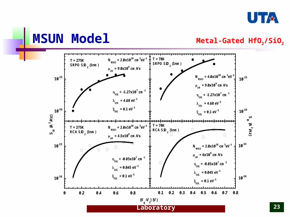
MSUN Model
10-17
10-16
10-15
1 10
RCA SiO2 (1nm)
(Vg -V
t) = 0.7V
T = 275K
10-16
10-15
SRPO SiO2 (1nm)
(Vg-V
t) = 0.7V
T = 275K
SId
(A
2/H
z)
= -1.27x107 cm-1
= 4.68 eV-1
= 0.1 eV-1
= -0.85x107 cm-1
= 0.045 eV-1
= 0.1 eV-1
f (Hz)
10-17
10-16
10-15
10 100
RCA SiO2 (1nm)
(Vg -V
t) = 0.3V
T = 78K
10-16
10-15
SRPO SiO2 (1nm)
(Vg -V
t) = 0.3V
T = 78K
SId (A
2/Hz)
= -1.27x107 cm-1
= 4.68 eV-1
= 0.1 eV-1
= -0.85x107 cm-1
= 0.045 eV-1
= 0.1 eV-1
Nt
= 2.0x1018 cm3eV-1
c0 = 9.0x109 cm/Vs
Nt
= 4.0x1018 cm3eV-1
c0 = 9.0x109 cm/Vs
Nt
= 2.0x1018 cm3eV-1
c0 = 4.5x108 cm/Vs
Nt
= 2.0x1018 cm3eV-1
c0 = 6x108 cm/Vs
Metal-Gated HfO2/SiO2
UTA Noise and Reliability Laboratory 23
MSUN Model
10-16
10-15
0 0.2 0.4 0.6 0.8
T = 275KRCA SiO
2 (1nm)
10-16
10-15
T = 78KSRPO SiO
2 (1nm)
10-16
10-15
T = 275KSRPO SiO
2 (1nm)
SId
(A2/H
z)
(Vg-V
t) (V)
= -1.27x107 cm-1
= 4.68 eV-1
= 0.1 eV-1
= -0.85x107 cm-1
= 0.045 eV-1
= 0.1 eV-1
SId (A
2/Hz)
Nt
= 2.0x1018 cm3eV-1
c0 = 9.0x109 cm/Vs
Nt
= 2.0x1018 cm3eV-1
c0 = 4.5x108 cm/Vs
Nt
= 4.0x1018 cm3eV-1
c0 = 9.0x109 cm/Vs
Nt
= 2.0x1018 cm3eV-1
c0 = 6x108 cm/Vs
= -1.27x107 cm-1
= 4.68 eV-1
= 0.1 eV-1
10-16
10-15
0.1 0.2 0.3 0.4 0.5 0.6 0.7 0.8
T = 78KRCA SiO
2 (1nm)
= -0.85x107 cm-1
= 0.045 eV-1
= 0.1 eV-1
Metal-Gated HfO2/SiO2

UTA Noise and Reliability Laboratory 24
Effective Oxide Trap Density vs. Temperature
NtH
K0 (
cm
-3e
V-1)
c0 (c
mV
-1S-1)
1018
1019
109
1010
SRPO SiO2 (1nm)
1018
4 1018
2 108
4 108
6 108
50 100 150 200 250 300 350 400Temperature (K)
RCA SiO2 (1nm)
Nt0HK is constant for all temperatures and the non-uniformity in trap density is modeled by ηHK ,λHK
Metal-Gated HfO2/SiO2
MSUN Model

UTA Noise and Reliability Laboratory 25
Effective Oxide Trap Density vs. Temperature
The overall effective trap density (Nt) is extracted using the Unified Flicker Noise Model.
In general, the values tend to increase with a decrease in temperature.
This is not consistent with the
uniform trap density assumption
at the core of the model.
Temperature (K)
Nt (
cm
-3eV
-1)
1016
1017
1018
1019
50 100 150 200 250 300 350 400
10Å SRPO SiO2
10Å RCA SiO2
Metal-Gated HfO2/SiO2
Original Unified Noise Model

UTA Noise and Reliability Laboratory 26
Outline
Noise Modeling Unified Flicker Noise Model Multi-Stack Unified Noise Model (MSUN)
Experimental Verification Metal-Gated HfO2/SiO2 NMOSFETs – different interfacial layer processing Poly-Gated HfSiON/SiON NMOSFETs – variable interfacial layer thickness
Conclusions and Future Work

UTA Noise and Reliability Laboratory 27
Poly Gated HfSiON/SiON MOSFETs NMOS HfSiON with same high-k thickness (3.0 nm) and
different interfacial layers (IL)
Dielectrics
EOT (nm)
IL (nm)Length (μm)
Width (μm)
Variable temperature 1/f noise measurementhas been done.
HfSiON 1.24 0.8 0.20 10
HfSiON1.33 1.0 0.20,0.25 10
HfSiON1.46 1.5 0.20,0.25 10
HfSiON1.66 1.8
0.14 ~ 0.25
10

UTA Noise and Reliability Laboratory 28
Temperature Dependence of Low Frequency Noise Spectral Density
•Normalized current noise spectral density did not show any noticeable dependence on temperature.
•The observed noise behavior is not affected by any temperature sensitive process.
•Remote optical phonon scattering may not have a significant impact on low frequency noise characteristics although it has a profound effect on mobility behavior (presented last year).
CE
OT
2(S
Id/I
d
2)
(F
2/H
z-cm
4)
EOT=1.24nm
EOT=1.46nm
10-21
10-20
10-19
10-18
10-21
10-20
10-19
160 180 200 220 240 260 280 300 320
Vg-V
t=0.2V
Vg-V
t=0.3V
Vg-V
t=0.4V
Vg-V
t=0.5V
Vg-V
t=0.6V
Vg-V
t=0.7V
Temperature (K)
Poly-Gated HfSiON / SiON

UTA Noise and Reliability Laboratory 29
Low Frequency Noise Mechanism
2
2 2
h eff dId
d d
q VS
I fL I
2 22
(1 / ) ( )Id meff ox d m Vfb
d d
S gC I g S
I I
Correlated Number and Mobility Fluctuation Model1:
Hooge’s Bulk Mobility Fluctuation Model9:
Correlated number and surface mobility fluctuation mechanism was observed to dominate for devices with different interfacial layer thicknesses in the experimental temperature range
9 F.N. Hooge. IEEE Trans. Electron Devices 41. 1926 (1994).
10-10
10-9
10-8
100
101
102
10-5 10-4 10-3
EOT=1.66 nm L=0.25m T=270K
(gm
/Id ) 2 (V-2)
Id(A)
SId
/Id
2 (H
z-1) 10-9
10-8
10-7
100
101
102
EOT=1.24 nm L=0.20m T=172K
Poly-Gated HfSiON / SiON

UTA Noise and Reliability Laboratory 30
The MSUN Model
),()1(),(2
fxSNN
IfxS
td Nd
I
According to original Unified Model, current noise spectral density can be shown as
Considering tunneling through a double step barrier, we can show
The final expression of Sid(A2/Hz) using the new model for high-k gate devices becomes
dzzzT
VqEENxkTW
dzzzT
VqEENxkTWS
HK
HKHK
TT
THK
HKHKifnHKtHK
IL
ILIL
T
IL
ILILifnILtILN
HKIL
IL
IL
t
220
220 0
1])(exp[4
1])(exp[4
(1)
(2)
(3)
dx
duu
u
f
EEN
duu
u
f
EEN
xNWL
kTIfS
HKHKHK
HK
HKHKHKHKHK
HKHKHKHKHKHKHKHKHKHK
ILILIL
IL
ILILILILIL
ILILILILILILILILILIL
dTf
f HK
HK
TVqHK
TVqTVqHKHK
ifnHKtHK
Tf
f IL
IL
TVqIL
TVqTVqILIL
ifnILtIL
L
effd
I
)exp(2
2 2
/)/(
/)/(1/)/(0
0
)exp(2
2 2
/)/(
/)/(1/)/(0
0
0
2
2
2
0
0
0
0
1)2(
)](exp[
1)2(
)](exp[
)(
14)(

UTA Noise and Reliability Laboratory 31
MSUN Model Parameter List
High-k dielectric layer parameters Interfacial layer parameters
NtHK0 Mid-gap trap density at the IL/high-k interface
NtIL0 Mid-gap trap density at the substrate/IL interface
μc0 Mobility fluctuation coefficient μc0 Mobility fluctuation coefficient
λHK Band bending parameter corresponding to the high-k layer
λIL Band bending parameter corresponding to the IL
ηHK Spatial trap distribution parameter for the high-k layer
ηIL Spatial trap distribution parameter for the interfacial layer
ξHK Parameter for the energy distribution of traps in the high-k dielectric layer
ξIL Parameter for the energy distribution of traps in the interfacial layer
• If the published trap density values are chosen for NtIL0 and NtHK0 the noise contribution of the interfacial layer is insignificant when compared to the total device noise. The interfacial layer parameters do not play any effective role in the data fitting• For the high-k layer, as discussed earlier, λHK= ξHK, so the number of effective fitting parameters reduce to 4.

UTA Noise and Reliability Laboratory 32
Extracted ξ, λ, η
From Eq (3) we can show
α=
From a linear fit of α as a function of Vg for individual devices at all temperatures, the energy dependence parameters ξ, λ and the spatial distribution parameter η were extracted. The extracted values are shown on the plots.
Poly-Gated HfSiON / SiON
HKHKHKHKHK TVq /)/(1
0
0.2
0.4
0.6
0.8
1
1.2
1.4
EOT=1.24nm
HK
=HK
=1.53 eV -1
HK
=-7.99x10 6 cm -1
EOT=1.33nm
HK
=HK
=-0.4056 eV -1
HK
=-5.38x10 6 cm -1
0
0.2
0.4
0.6
0.8
1
1.2
0.4 0.6 0.8 1 1.2
EOT=1.46nm
HK
=HK
=-0.455 eV -1
HK
=-4.67x10 6 cm-1
0.4 0.6 0.8 1 1.2 1.4
HK
=HK
=-0.947 eV -1
HK
=-3.53x10 6 cm -1
EOT=1.66nm
Vg (V)
Fre
qu
en
cy
ex
po
nen
t (
)

UTA Noise and Reliability Laboratory 33
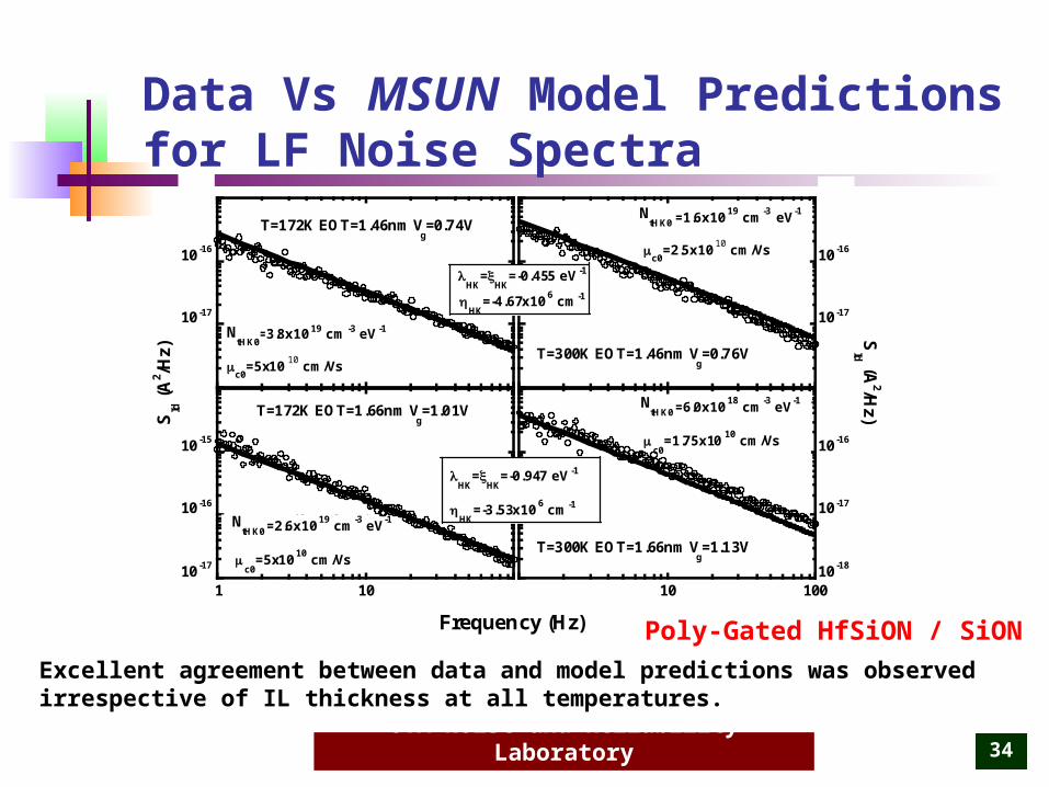
Data Vs MSUN Model Predictions for LF Noise Spectra
The calculated current noise spectral density SId is compared to the data for devices withfour different IL thicknesses and in the experimental temperature range of 172K-300K.
10 -17
10 -16
10 -15
1 10 10 0
Fr eq ue nc y (H z)
Nt0
=1.7x10¹⁹
cm-3
eV-1
c0
=5x10¹⁰
cm/Vs10-18
10-17
10-16
Nt0
=1.3x10¹⁹
cm-3
eV-1
c0
=5x10¹⁰
cm/Vs
Frequency (Hz)
SId (A
2/Hz)
SId (
A2 /H
z)
HK
=HK
=1.53 eV -1
HK
=-7.99x106 cm-1
T=172K EOT=1.24nm Vg=0.96V
T=172K EOT=1.33nm Vg=0.94V
T=300K EOT=1.24nm Vg=0.58V
T=300K EOT=1.33nm Vg=0.67V
Nt0HK
=3.0x10¹⁹
cm-3
eV-1
c0
=5x10¹⁰
cm/Vs
NtHK0
=1.3x10¹⁹
cm-3
eV-1
c0
=5x10¹⁰
cm/Vs
Nt0HK
=1.7x10¹⁹
cm-3
eV-1
c0
=5x10¹⁰
cm/Vs
10 -17
10 -16
10 -15
1 10 100
Nt0HK
=6.4x10¹⁹
cm-3
eV-1
c0
=1.1x10¹⁰
cm/Vs
10-17
10-16
10-15
10 100
HK
=-5.38x106 cm-1
HK
=HK
=-0.4056 eV -1
NtHK0
NtHK0
NtHK0
Poly-Gated HfSiON / SiON
UTA Noise and Reliability Laboratory 34
Data Vs MSUN Model Predictions for LF Noise Spectra
Excellent agreement between data and model predictions was observed irrespective of IL thickness at all temperatures.
Poly-Gated HfSiON / SiON
10 -17
10 -16
10 -15
1 10 100
Nt0
=2.6x10¹⁹
cm-3
eV-1
c0
=5x10 10 cm/Vs 10 -18
10 -17
10 -16
10 100
Nt0
=6.0x10¹⁸
cm-3
eV-1
c0
=1.75x10¹⁰
cm/Vs
Frequency (Hz)
SId (A
2/Hz)S
Id (
A2 /H
z)
HK
=HK
=-0.947 eV -1
HK
=-3.53x106 cm-1
T=300K EOT=1.66nm Vg=1.13V
T=172K EOT=1.46nm Vg=0.74V
T=172K EOT=1.66nm Vg=1.01V
T=300K EOT=1.46nm Vg=0.76V
Nt0HK
=6.0x10¹⁸
cm-3
eV-1
c0
=1.75x10¹⁰
cm/Vs
Nt0HK
=2.6x10¹⁹
cm-3
eV-1
c0
=5x10¹⁰
cm/Vs
10 -17
10 -16
Nt0HK
=3.8x10 19 cm -3 eV -1
c0
=5x10¹⁰
cm/Vs
10 -17
10 -16
Nt0HK
=1.6x10¹⁹
cm-3
eV-1
c0
=2.5x10¹⁰
cm/Vs
HK
=HK
=-0.455 eV -1
HK
=-4.67x106 cm-1
NtHK0
NtHK0
NtHK0
NtHK0

UTA Noise and Reliability Laboratory 35
Data Vs MSUN Model Predictions for LF Noise Spectra
10-21
10-20
10-19
10-18
10-17
10-16
10-15
1 10 100 1000
SId Total
SId high-
SId ILS
Id(A
2 /Hz)
Frequency (Hz)
EOT=1.66nm
A special phenomena was observed for the devices with the thickest gate oxide.
The higher frequency components in the device noise are contributed by traps closer to the interface, where as the traps further away contribute to the lower frequency components.
For the devices with TIL=1.8nm, the characteristic corner frequency was calculated to be fc2~ 33Hz. Below 33 Hz the noise was contributed by the high-k layer. Above this limit noise contribution was primarily from the IL layer.
Frequency (Hz)
SId (A2/Hz)
)2(1 02 HKcf
))exp(2(1 01 HKHKHKc Tf
fα=0
α~1
α~2

UTA Noise and Reliability Laboratory 36
Data Vs MSUN Model Predictions for Bias Dependence
• The fit was good in the bias range of moderate inversion to strong inversion, for devices with all different IL thick-nesses in the experimental temperature range.
Poly-Gated HfSiON / SiON(V
g-V
t ) (V)
SId (
A2 /H
z)
10 -16
10 -15
==1.53 eV-1
=-7.99x106 cm-1
Nt0
=1.9x10¹⁹
cm-3
eV-1
c0
=2.75x1010 cm/Vs
EOT=1.28nm T=230K
0.1 0.2 0.3 0.4 0.5 0.6 0.7 0.8
==-0.947 eV-1
=-3.53x106 cm-1
Nt0
=2.3x1019 cm-3 eV -1
c0
=5.0x1010 cm/Vs
EOT =1.66nm T =188K
10-14
Nt0HK
=1.9x10¹⁹
cm-3 eV
-1
c0
=2.75x10¹⁰
cm/Vs
EOT=1.24nm T=230K
HK
=HK
=1.53 eV -1
HK
=-7.99x106 cm-1
HK
=HK
=-0.947 eV -1
HK
=-3.53x106 cm-1
Nt0HK
=2.3x10¹⁹
cm-3 eV
-1
c0
=5.0x10¹⁰
cm/Vs
EOT=1.66nm T=188K10 -16
10 -15
0 0.1 0.2 0.3 0.4 0.5 0.6 0.7
HK
=HK
=-0.455 eV-1
HK
=-4.67x106 cm-1
Nt0HK
=1.9x1019 cm-3 eV-1
c0
=5.0x1010 cm/Vs
EOT=1.46nm T=261K
Nt0HK
=6.4x10¹⁹
cm-3
eV-1
c0
=1.1x1010 cm/Vs
EOT=1.33nm T=172K
HK
=HK
=-0.4056 eV-1
HK
=-5.38x106 cm
-1
NtHK0
NtHK0 N
tHK0
NtHK0

UTA Noise and Reliability Laboratory 37
Extracted MSUN Model Parameters
EOT=1.28nm, λHK=ξHK =1.538eV-1, ηHK =-7.99x10 6 cm-1 EOT=1.33nm, λHK=ξHK =-0.4056eV-1, ηHK=-5.38x10 6 cm-1
T(K) NtHK0(cm-3 eV-1) μc0(cm/Vs) T(K) NtHK0(cm-3 eV-1) μc0(cm/Vs)
172 1.7x10¹⁹ 5.0x10¹⁰ 172 6.4x10¹⁹ 1.1x10¹⁰
188 1.8x10¹⁹ 5.0x10¹⁰ 188 6.1x10¹⁹ 3.0x10¹⁰
207 1.7x10¹⁹ 3.0x10¹⁰ 207 5.6x10¹⁹ 4.5x10¹⁰
230 1.9x10¹⁹ 2.75x10¹⁰ 230 5.9x10¹⁹ 3.5x10¹⁰
261 1.4x10¹⁹ 5.0x10¹⁰ 261 3.6x10¹⁹ 1.7x10¹⁰
300 1.3x10¹⁹ 5.0x10¹⁰ 300 3.0x10¹⁹ 5.0x10¹⁰
EOT=1.46nm, λHK=ξ HK = -0.455eV-1, η HK=-4.67x10 6 cm-1 EOT=1.66nm, λHK=ξ HK = -0.947eV-1, η HK=-3.53x10 6 cm-1
T(K) NtHK0(cm-3 eV-1) μc0(cm/Vs) T(K) NtHK0(cm-3 eV-1) μc0(cm/Vs)
172 3.8x10¹⁹ 5.0x10¹⁰ 172 2.6x10¹⁹ 5.0x10¹⁰
188 3.1x10¹⁹ 5.0x10¹⁰ 188 2.3x10¹⁹ 5.0x10¹⁰
207 2.4x10¹⁹ 5.0x10¹⁰ 207 1.4x10¹⁹ 7.5x10¹⁰
230 1.5x10¹⁹ 2.25x10¹⁰ 230 1.6x10¹⁹ 5.0x10¹⁰
261 1.9x10¹⁹ 5.0x10¹⁰ 250 1.6x10¹⁹ 5.0x10¹⁰
300 1.6x10¹⁹ 2.5x10¹⁰ 270 9.0x10¹⁸ 3.0x10¹⁰
300 6.0x10¹⁸ 1.75x10¹⁰Poly-Gated HfSiON / SiON
UTA Noise and Reliability Laboratory 38
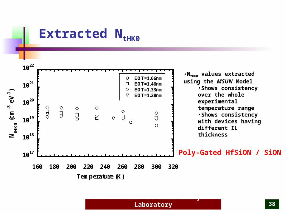
Extracted NtHK0
•NtHK0 values extracted using the MSUN Model
•Shows consistency over the whole experimental temperature range•Shows consistency with devices having different IL thickness
Poly-Gated HfSiON / SiON1017
1018
1019
1020
1021
1022
160 180 200 220 240 260 280 300 320
EOT=1.66nmEOT=1.46nmEOT=1.33nmEOT=1.28nm
Temperature (K)
NtH
K0 (
cm
-3 e
V-1
)

UTA Noise and Reliability Laboratory 39
Dependence of NtHK on Energy
The active trap densities asprobed by the quasi-Fermienergy and it’s excursion is shown for devices with different IL thicknesses.
As the excursion range is comparatively small, the calculated trap density out-side the highlighted regionmay not correctly representactual device characteristics.
At 300K, the active trap density was observed to beIL dependent. The thinnestgate oxide devices showedhighest active trap density.
Poly-Gated HfSiON / SiON
EOT=1.46nm
EOT=1.24nm
EOT=1.33nm
Eg(eV)
EOT=1.66nmNtH
K=
NtH
K0e
xp(
|E-E
i|) (
cm
-3 e
V-1
)
1019
1020
Nt0
=1.3x10¹⁹
cm-3
eV-1
c0
=5x10¹⁰
cm/Vs
==1.53 eV-1
=-7.99x106 cm-1
Fermi energy sweep range
(3.0x10¹⁹ ~ 3.4x10¹⁹)cm-3eV-1
EV
EC
1019
1020
Fermi energy sweep range
(2.33x10¹⁹
~ 2.39x10¹⁹
)cm-3
eV-1
Nt0
=3.0x1019 cm-3 eV-1
c0
=5x1010 cm/Vs
==-0.4056 eV-1
=-5.38x106 cm-1
EV E
C
2 1018
1019
-0.2 0 0.2 0.4 0.6 0.8 1 1.2 1.4
EV
EC
==-0.947 eV-1
=-3.53x106 cm-1
Nt0
=6.0x1018 cm-3 eV-1
c0
=1.75x1010 cm/Vs
Fermi energy sweep range
(3.37x10 18 ~ 3.54x10 18)cm -3eV -1
2 1019 2 1019
Nt0HK
=1.3x1019 cm -3 eV -1
c0
=5x1010 cm/Vs
HK
=HK
=1.53 eV -1
HK
=-7.99x106 cm-1
Nt0HK
=3.0x10¹⁹
cm-3
eV-1
c0
=5x10¹⁰
cm/Vs
HK=
HK=-0.4056 eV-1
HK
=-5.38x106 cm -1
HK
=HK
=-0.947 eV-1
HK
=-3.53x106 cm -1
Nt0HK
=6.0x1018 cm -3 eV -1
c0
=1.75x1010 cm/Vs
5 1018
4 1019
-0.2 0 0.2 0.4 0.6 0.8 1 1.2
EV
EC
HK
=HK
=-0.455 eV-1
HK
=-4.67x10 6 cm-1
Nt0 HK
=1.60x10¹⁹
cm-3
eV-1
c0
=2.5x10¹⁰
cm/Vs
Fermi energy sweep range
(1.31x10¹⁹
~ 1.34x10¹⁹
)cm-3
eV-1
NtHK0
NtHK0
NtHK0
NtHK0

UTA Noise and Reliability Laboratory 40
Results I
The temperature dependence of extracted trap density is inconsistent with the core model assumption.
Multi-Stack Unified Noise (MSUN) model is proposed to predict noise in high-k/interfacial layer MOSFETs.
It is scalable with respect to HK/IL thicknesses, temperature and applied bias.
It accounts for the material properties of constituent dielectric materials and the non-uniform dielectric trap density profile with respect to energy and location in dielectric.
Four model parameters Mid-gap trap density at the IL/high-k interface Parameter for the energy distribution of traps in the high-k dielectric layer Spatial trap distribution parameter for the high-k layer Mobility fluctuation coefficient

UTA Noise and Reliability Laboratory 41
Results II
• The model is in excellent agreement with the experimental data down to cryogenic temperatures. Metal-Gated HfO2/SiO2 NMOSFETs – different interfacial layer
processing Poly-Gated HfSiON/SiON NMOSFETs – variable interfacial layer
thickness• Metal-Gated HfSiON/SiON MOSFETs – different nitridation techniques
UTA Noise and Reliability Laboratory 42
Acknowledgements
Thanks to
Luigi Colombo, Texas InstrumentsKeith Green, Texas InstrumentsAjit Shanware, Texas InstrumentsHsing-Huang Tseng, FreescaleAnia Zlotnicka, Freescale Manuel Quevedo-Lopez, Texas Instruments / SEMATECH