noip1sn5000a - python 5.0/2.0 megapixels global … · noip1sn5000a 2 ordering information part...
TRANSCRIPT

© Semiconductor Components Industries, LLC, 2016
August, 2016 − Rev. 11 Publication Order Number:
NOIP1SN5000A/D
NOIP1SN5000A
PYTHON 5.0/2.0 MegaPixelsGlobal Shutter CMOS Image Sensors
Features
• Data Output Options♦ P1: 8 LVDS Data Channels♦ P3: 4 LVDS Data Channels
• Size Options♦ PYTHON 2000: 1920 x 1200 Active Pixels, 2/3” Optical Format♦ PYTHON 5000: 2592 x 2048 Active Pixels, 1” Optical Format
• 4.8 �m x 4.8 �m Low Noise Global Shutter Pixels withIn-pixel CDS
• Monochrome (SN), Color (SE) and NIR (FN)• Zero Row Overhead Time Mode Enabling Higher Frame Rate• Frame Rate at Full Resolution, 8 LVDS Data Channels (P1 only)
♦ 100/85 frames per second @ 5 MP (Zero ROT/Non−Zero ROT)♦ 230/180 frames per second @ 2 MP (Zero ROT/Non−Zero ROT)♦ 255/200 frames per second @ Full HD (Zero ROT/Non−Zero ROT)
• On-chip 10-bit Analog-to-Digital Converter (ADC)
• Eight/Four/Two/One LVDS High Speed Serial Outputs
• Random Programmable Region of Interest (ROI) Readout
• Serial Peripheral Interface (SPI)
• Automatic Exposure Control (AEC)
• Phase Locked Loop (PLL)
• High Dynamic Range (HDR) Modes Possible
• Dual Power Supply (3.3 V and 1.8 V)
• −40°C to +85°C Operational Temperature Range• 84-pin LCC• Power Dissipation
♦ 1.45 W (P1, 8 LVDS, NZROT)♦ 925 mW (P1, P3, 4 LVDS, NZROT)♦ 520 mW (P1, P3, 2 LVDS, NZROT)♦ 370 mW (P1, P3, 1 LVDS, NZROT)
• These Devices are Pb−Free and are RoHS Compliant
Applications• Machine Vision• Motion Monitoring• Security• Intelligent Traffic Systems (ITS)
DescriptionThe PYTHON 2000 and PYTHON 5000 image sensors
utilize high sensitivity 4.8 �m x 4.8 �m pixels that supportlow noise “pipelined” and “triggered” global shutter readoutmodes. The sensors support correlated double sampling(CDS) readout, reducing noise and increasing dynamicrange.
The sensor has on-chip programmable gain amplifiers and10-bit A/D converters. The integration time and gainparameters can be reconfigured without any visible imageartifact. Optionally the on-chip automatic exposure controlloop (AEC) controls these parameters dynamically. Theimage’s black level is either calibrated automatically or canbe adjusted by adding a user programmable offset.
A high level of programmability using a four wire serialperipheral interface enables the user to read out specificregions of interest. Up to sixteen regions can beprogrammed, achieving even higher frame rates.
The image data interface of the P1 devices consists ofeight LVDS lanes, facilitating frame rates up to 100 framesper second in Zero ROT mode for the PYTHON 5000. Eachchannel runs at 720 Mbps. A separate synchronizationchannel containing payload information is provided tofacilitate the image reconstruction at the receiving end.
The P3 devices are the same as the P1 but with only fourof the eight LVDS data channels enabled, facilitating framerates of 45 frames per second in Non Zero ROT (NZROT)for the PYTHON 5000.
www.onsemi.com
Figure 1. PYTHON 5000

NOIP1SN5000A
www.onsemi.com2
ORDERING INFORMATION
Part Number Description Package
PYTHON 5000
NOIP1SN5000A−QDI 5 MegaPixel, Monochrome 84−pin LCC
NOIP1SE5000A−QDI 5 MegaPixel, Bayer Color
NOIP1FN5000A−QDI 5 MegaPixel, Monochrome with enhanced NIR
NOIP1SN5000A−QTI 5 MegaPixel, Monochrome, Protective Film
NOIP1SE5000A−QTI 5 MegaPixel, Bayer Color, Protective Film
NOIP1FN5000A−QTI 5 MegaPixel, Monochrome with enhanced NIR, Protective Film
NOIP3SN5000A−QDI 5 MegaPixel, 4 LVDS Outputs, Monochrome
NOIP3SE5000A−QDI 5 MegaPixel, 4 LVDS Outputs, Bayer Color
NOIP3FN5000A−QDI 5 MegaPixel, 4 LVDS Outputs, Monochrome with enhanced NIR
NOIP3SN5000A−QTI 5 MegaPixel, 4 LVDS Outputs, Monochrome, Protective Film
NOIP3SE5000A−QTI 5 MegaPixel, 4 LVDS Outputs, Bayer Color, Protective Film
NOIP3FN5000A−QTI 5 MegaPixel, 4 LVDS Outputs, Monochrome with enhanced NIR, Protective Film
PYTHON 2000
NOIP1SN2000A−QDI 2 MegaPixel, Monochrome 84−pin LCC
NOIP1SE2000A−QDI 2 MegaPixel, Bayer Color
NOIP1FN2000A−QDI 2 MegaPixel, Monochrome with enhanced NIR
NOIP1SN2000A−QTI 2 MegaPixel, Monochrome, Protective Film
NOIP1SE2000A−QTI 2 MegaPixel, Bayer Color, Protective Film
NOIP1FN2000A−QTI 2 MegaPixel, Monochrome with enhanced NIR, Protective Film
The P1−SN/SE/FN base part references the mono, colorand NIR enhanced versions of the 8 LVDS interface; theP3−SN/SE/FN base part references the mono, color and NIRenhanced version of the 4 LVDS interface. More details onthe part number coding can be found athttp://www.onsemi.com/pub_link/Collateral/TND310−D.PDF
Package MarkLine 1: NOI Pyxx RRRRA where xx denotes mono
micro lens (SN) or color micro lens (SE) option or NIRmicro lens (FN), RRRR is the resolution (5000), (2000); y is either 1 for 8 LVDS outputs available or 3 for 4 LVDSoutputs bonded
Line 2: −QDI (without protective film), −QTI (withprotective film)
Line 3: AWLYYWW where AWL is PRODUCTION lottraceability, YYWW is the 4−digit date code

NOIP1SN5000A
www.onsemi.com3
SPECIFICATIONS
Key Specifications
Table 1. GENERAL SPECIFICATIONS (Note 1)
Parameter Specification
Pixel Type In−pixel CDS. Global shutter pixel architecture
Shutter Type Pipelined and triggered global shutter
Frame Rate Zero ROT/ Non−Ze-ro ROT Mode
P1−SN/SE/FN:PYTHON 2000: 230/180 fpsPYTHON 5000: 100/85 fps
P3−SN/SE/FN: NA/45 fps
Master Clock P1,P3−SN/SE/FN:72 MHz when PLL is used,360 MHz (10-bit) / 288 MHz (8-bit) whenPLL is not used
Windowing 16 Randomly programmable windows. Normal, sub-sampled and binned readoutmodes
ADC Resolution(Note 1)
10-bit, 8-bit
LVDS Outputs P1−SN/SE/FN: 8/4/2/1 data + sync + clock
P3−SN/SE/FN: 4/2/1 data + sync + clock
Data Rate P1−SN/SE/FN:8 x 720 Mbps (10-bit) / 8 x 576 Mbps (8-bit)
P3−SN/SE/FN:4 x 720 Mbps (10−bit)
Power Dissipation(10−bit mode)
P1−SN/SE/FN: 1.45 W (8 data channels)P1&P3−SN/SE/FN: 925 mW (4 data channels)P1&P3−SN/SE/FN: 520 mW (2 data channels)P1&P3−SN/SE/FN: 370 mW (1 data channel)
Package Type 84-pin LCC
Table 2. NOMINAL ELECTRO−OPTICALSPECIFICATIONS
Parameter Specification
Active Pixels PYTHON 5000: 2592 (H) x 2048 (V)PYTHON 2000: 1984 (H) x 1264 (V)
Pixel Size 4.8 �m x 4.8 �m
Conversion Gain 0.096 LSB10/e-, 140 �V/e-
Temporal Noise < 10.7 e- (Non−Zero ROT, 1x gain)< 9.4 e- (Non−Zero ROT, 2x gain)
Responsivity at 550 nm 7.5 V/lux.s
Parasitic Light
Sensitivity (PLS)
<1/5000
Full Well Charge 10000 e-
Quantum Efficiency at 550 nm
57%
Pixel FPN < 1.55 LSB10 (Non−Zero ROT)< 1.35 (Zero−ROT)
PRNU < 10 LSB10 on half scale response of525 LSB10
MTF 66% @ 535 nm − X-dir & Y-dir
Pixel Storage Node Leakage(PSNL) @ 20°C (t_int = 30 ms)
300 LSB10/s, 2800 e-/s
Dark Signal @ 20°C 9.3 e-/s, 1.0 LSB10/s
Dark Current Doubling Temperature
5.2°C
Dynamic Range 60 dB
Signal to Noise Ratio (SNR max)
40 dB
Table 3. RECOMMENDED OPERATING RATINGS (Note 2)
Symbol Description Min Max Unit
TJ Operating junction temperature range −40 85 °C
Functional operation above the stresses listed in the Recommended Operating Ranges is not implied. Extended exposure to stresses beyondthe Recommended Operating Ranges limits may affect device reliability.
Table 4. ABSOLUTE MAXIMUM RATINGS (Notes 3 and 4)
Symbol Parameter Min Max Unit
ABS (1.8 V supply group) ABS rating for 1.8 V supply group –0.5 2.2 V
ABS (3.3 V supply group) ABS rating for 3.3 V supply group –0.5 4.3 V
TS ABS storage temperature range −40 +150 °C
ABS storage humidity range at 85°C 85 %RH
Electrostatic discharge (ESD) Human Body Model (HBM): JS−001−2012 2000 V
Charged Device Model (CDM): EIA/JESD22−C101, Class C1 500
LU Latch−up: JESD−78 100 mA
Stresses exceeding those listed in the Maximum Ratings table may damage the device. If any of these limits are exceeded, device functionalityshould not be assumed, damage may occur and reliability may be affected.1. The ADC is 11−bit, down−scaled to 10−bit. The PYTHON uses a larger word−length internally to provide 10−bit on the output.2. Operating ratings are conditions in which operation of the device is intended to be functional.3. ON Semiconductor recommends that customers become familiar with, and follow the procedures in JEDEC Standard JESD625−A. Refer
to Application Note AN52561. Long term exposure toward the maximum storage temperature will accelerate color filter degradation.4. Caution needs to be taken to avoid dried stains on the underside of the glass due to condensation. The glass lid glue is permeable and can
absorb moisture if the sensor is placed in a high % RH environment.

NOIP1SN5000A
www.onsemi.com4
Table 5. ELECTRICAL SPECIFICATIONSBoldface limits apply for TJ = TMIN to TMAX, all other limits TJ = +30°C. (Notes 5, 6, 7, 8 and 9)
Parameter Description Min Typ Max Units
Power Supply Parameters − P1 − SN/SE/FN (ZROT)(Note: All ground pins (gnd_18, gnd_33 and gnd_colpc) should be connected to an external 0 V ground reference.)
vdd_33 Supply voltage, 3.3 V 3.2 3.3 3.4 V
Idd_33 Current consumption 3.3 V supply 310 mA
vdd_18 Supply voltage, 1.8 V 1.7 1.8 1.9 V
Idd_18 Current consumption 1.8 V supply 140 mA
vdd_pix Supply voltage, pixel 3.25 3.3 3.35 V
Idd_pix Current consumption pixel supply 10 mA
Ptot Total power consumption at vdd_33 = 3.3 V, vdd_18 = 1.8 V 1.45 W
Pstby_lp Power consumption in low power standby mode 50 mW
Popt Power consumption at lower pixel rates Configurable
Power Supply Parameters − P3 − SN/SE/FN (NZROT)(Note: All ground pins (gnd_18, gnd_33 and gnd_colpc) should be connected to an external 0 V ground reference.)
vdd_33 Supply voltage, 3.3 V 3.2 3.3 3.4 V
Idd_33 Current consumption 3.3 V supply (4/2/1 LVDS) 180 / 110 / 70 mA
vdd_18 Supply voltage, 1.8 V 1.7 1.8 1.9 V
Idd_18 Current consumption 1.8 V supply (4/2/1 LVDS) 106 / 87 / 76 mA
vdd_pix Supply voltage, pixel 3.25 3.3 3.35 V
Idd_pix Current consumption pixel supply (4/2/1 LVDS) 6 / 3 / 1 mA
Ptot Total power consumption at vdd_33 = 3.3 V, vdd_18 = 1.8 VP3, 4 LVDS, NZROTP3, 2 LVDS, NZROTP3, 1 LVDS, NZROT
925520370
mW
Pstby_lp Power consumption in low power standby mode 50 mW
Popt Power consumption at lower pixel rates Configurable
I/O − P1,P3 − SN/SE/FN (EIA/TIA−644): Conforming to standard/additional specifications and deviations listed
fserdata Data rate on data channelsDDR signaling − 4 data channels, 1 synchronization channel
720 Mbps
fserclock Clock rate of output clockClock output for mesochronous signaling
360 MHz
Vicm LVDS input common mode level 0.3 1.25 1.8 V
Tccsk Channel to channel skew (Training pattern should be used to correctper channel skew)
50 ps
Electrical Interface − P1,P3 − SN/SE/FN
fin Input clock rate when PLL used 72 MHz
fin Input clock when LVDS input used 360 MHz
tidc Input clock duty cycle when PLL used 45 50 55 %
tj Input clock jitter 20 ps
fspi SPI clock rate when PLL used at fin = 72 MHz 10 MHz
ratspi (=fin/fspi) 10−bit (8 LVDS channels), PLL used (fin = 72 MHz) − P1 only 6
10−bit (4 LVDS channels), PLL used (fin = 72 MHz) 12
10−bit (2 LVDS channels), PLL used (fin = 72 MHz) 24
10−bit (1 LVDS channel), PLL used (fin = 72 MHz) 48
10−bit (8 LVDS channels), LVDS input used (fin = 360 MHz) 30
10−bit (4 LVDS channels), LVDS input used (fin = 360 MHz) 60
Product parametric performance is indicated in the Electrical Characteristics for the listed test conditions, unless otherwise noted. Productperformance may not be indicated by the Electrical Characteristics if operated under different conditions.5. All parameters are characterized for DC conditions after thermal equilibrium is established.6. This device contains circuitry to protect the inputs against damage due to high static voltages or electric fields. However, it is
recommended that normal precautions be taken to avoid application of any voltages higher than the maximum rated voltages to this highimpedance circuit.
7. Minimum and maximum limits are guaranteed through test and design.8. Refer to ACSPYTHON5000 available at CISP extranet for detailed acceptance criteria specifications.9. For power supply management recommendations, please refer to Application Note AND9158.

NOIP1SN5000A
www.onsemi.com5
Table 5. ELECTRICAL SPECIFICATIONSBoldface limits apply for TJ = TMIN to TMAX, all other limits TJ = +30°C. (Notes 5, 6, 7, 8 and 9)
Parameter UnitsMaxTypMinDescription
Electrical Interface − P1,P3 − SN/SE/FN
10−bit (2 LVDS channels), LVDS input used (fin = 360 MHz) 120
10−bit (1 LVDS channel), LVDS input used (fin = 360 MHz) 240
8−bit (8 LVDS channels), PLL used (fin = 72 MHz) 6
8−bit (4 LVDS channels), PLL used (fin = 72 MHz) 12
8−bit (2 LVDS channels), PLL used (fin = 72 MHz) 24
8−bit (1 LVDS channel), PLL used (fin = 72 MHz) 48
8−bit (8 LVDS channels), LVDS input used (fin = 288 MHz) 24
8−bit (4 LVDS channels), LVDS input used (fin = 288 MHz) 48
8−bit (2 LVDS channels), LVDS input used (fin = 288 MHz) 96
8−bit (1 LVDS channel), LVDS input used (fin = 288 MHz) 192
Frame Specifications − P1 − SN/SE/FN
Maximum
UnitsNon−Zero ROT Zero ROT
fps_roi1 Xres x Yres = 2592 x 2048 85 100 fps
fps_roi2 Xres x Yres = 2048 x 2048 100 130 fps
fps_roi3 Xres x Yres = 1920 x 1200 180 230 fps
fps_roi4 Xres x Yres = 1920 x 1080 200 255 fps
fps_roi5 Xres x Yres = 1600 x 1200 205 275 fps
fps_roi6 Xres x Yres = 1024 x 1024 395 480 fps
fps_roi7 Xres x Yres = 1280 x 720 390 550 fps
fps_roi8 Xres x Yres = 800 x 600 620 985 fps
fps_roi9 Xres x Yres = 640 x 480 855 1450 fps
fps_roi10 Xres x Yres = 512 x 512 890 1555 fps
fps_roi11 Xres x Yres = 256 x 256 2065 2830 fps
fps_roi12 Xres x Yres = 544 x 20 7980 10345 fps
fpix Pixel rate (8 channels at 72 Mpix/s) 576 576 Mpix/s
Frame Specifications − P3 − SN/SE/FN
Maximum
Units4 LVDS 2 LVDS 1 LVDS
fps_roi1 Xres x Yres = 2592 x 2048 45 25 10 fps
fps_roi2 Xres x Yres = 2048 x 2048 55 30 15 fps
fps_roi3 Xres x Yres = 1920 x 1200 100 55 25 fps
fps_roi4 Xres x Yres = 1920 x 1080 110 60 30 fps
fps_roi5 Xres x Yres = 1600 x 1200 115 60 30 fps
fps_roi6 Xres x Yres = 1024 x 1024 195 105 55 fps
fps_roi7 Xres x Yres = 1280 x 720 230 125 65 fps
fps_roi8 Xres x Yres = 800 x 600 385 220 115 fps
fps_roi9 Xres x Yres = 640 x 480 550 320 175 fps
fps_roi10 Xres x Yres = 512 x 512 590 350 190 fps
fps_roi11 Xres x Yres = 256 x 256 1590 990 580 fps
fps_roi12 Xres x Yres = 544 x 20 6260 4340 2690 fps
fpix Pixel rate (8 channels at 72 Mpix/s) 288 144 72 Mpix/s
Product parametric performance is indicated in the Electrical Characteristics for the listed test conditions, unless otherwise noted. Productperformance may not be indicated by the Electrical Characteristics if operated under different conditions.5. All parameters are characterized for DC conditions after thermal equilibrium is established.6. This device contains circuitry to protect the inputs against damage due to high static voltages or electric fields. However, it is
recommended that normal precautions be taken to avoid application of any voltages higher than the maximum rated voltages to this highimpedance circuit.
7. Minimum and maximum limits are guaranteed through test and design.8. Refer to ACSPYTHON5000 available at CISP extranet for detailed acceptance criteria specifications.9. For power supply management recommendations, please refer to Application Note AND9158.

NOIP1SN5000A
www.onsemi.com6
Color Filter ArrayThe PYTHON color sensors are processed with a Bayer RGB color pattern as shown in Figure 2. Pixel (0,0) has a red filter
situated to the bottom left.
Figure 2. Color Filter Array for the Pixel Array
pixel (0;0)
Y
X
Gb
Gr
Quantum Efficiency
Figure 3. Quantum Efficiency Curves

NOIP1SN5000A
www.onsemi.com7
Ray Angle and Microlens Array InformationAn array of microlenses is placed over the CMOS pixel
array in order to improve the absolute responsivity of thephotodiodes. The combined microlens array and pixel arrayhas two important properties:
Angular Dependency of Photoresponse of a PixelThe photoresponse of a pixel with microlens in the center
of the array to a fixed optical power with varied incidenceangle is as plotted in Figure 4, where definitions of angles�x and �y are as described by Figure 5.
Microlens Shift across Array and CRAThe microlens array is fabricated with a slightly smaller
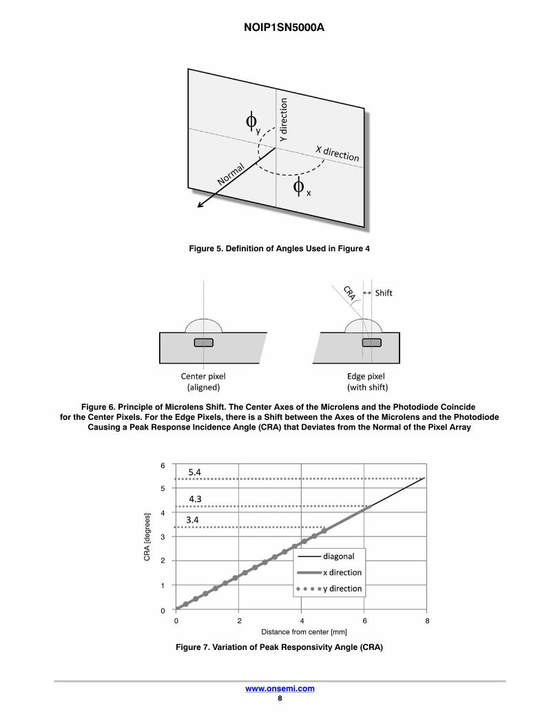
pitch than the array of photodiodes. This difference in pitchcreates a varying degree of shift of a pixel’s microlens withregards to its photodiode. A shift in microlens position
versus photodiode position will cause a tilted angle of peakphotoresponse, here denoted Chief Ray Angle (CRA).Microlenses and photodiodes are aligned with 0 shift andCRA in the center of the array, while the shift and CRAincreases radially towards its edges, as illustrated byFigure 6.
The purpose of the shifted microlenses is to improve theuniformity of photoresponse when camera lenses witha finite exit pupil distance are used. In the standard versionof Python 5000, the CRA varies nearly linearly with distancefrom the center as illustrated in Figure 7, with a corner CRAof approximately 5.4 degrees. This edge CRA is matchinga lens with exit pupil distance of ~80 mm.
Figure 4. Center Pixel Photoresponse to a Fixed Optical Power with Incidence Angle Varied along �x and �y. Note that the Photoresponse Peaks near Normal Incidence for Center Pixels
NOIP1SN5000A
www.onsemi.com8
Figure 5. Definition of Angles Used in Figure 4
Figure 6. Principle of Microlens Shift. The Center Axes of the Microlens and the Photodiode Coincide for the Center Pixels. For the Edge Pixels, there is a Shift between the Axes of the Microlens and the Photodiode
Causing a Peak Response Incidence Angle (CRA) that Deviates from the Normal of the Pixel Array
Figure 7. Variation of Peak Responsivity Angle (CRA)
0
1
2
3
4
5
6
0 2 4 6 8
Distance from center [mm]
CR
A [d
egre
es]

NOIP1SN5000A
www.onsemi.com9
OVERVIEW
Figures 8 gives an overview of the major functional blocks of the PYTHON sensor.
Figure 8. Block Diagram
Pixel Array
Analog Front End (AFE)
Data Formatting
Serializers & LVDS Interface
LVDS ClockInput
16 Analog channels
16 x 10 bitDigital channels
8 x 10 bitDigital channels
Row
Dec
oder
Column Structure
Image Core Bias
Image Core
AutomaticExposureControl(AEC)
ClockDistribution
CMOS ClockInput
LVDSReceiver
PLL
Control &Registers
Re
set
Ext
erna
l Tr
igge
rs
SP
I Int
erfa
ce
8/4/2/1 LVDS Channels1 LVDS Sync Channel1 LVDS Clock Channel
Image Core
The image core consists of:• Pixel Array
• Address Decoders and Row Drivers
• Pixel BiasingThe PYTHON 5000 pixel array contains 2592 (H) x
2048 (V) readable pixels with a pixel pitch of 4.8 �m.The PYTHON 2000 image array contains 1984 (H) x
1264 (V) readable pixels, inclusive of 32 pixels on each sideto allow for reprocessing or color reconstruction.
The sensors use in−pixel CDS architecture, which makesit possible to achieve a low noise read out of the pixel arrayin global shutter mode with the function of the row driversis to access the image array to reset or read the pixel data. Therow drivers are controlled by the on−chip sequencer and canaccess the pixel array.
The pixel biasing block guarantees that the data on a pixelis transferred properly to the column multiplexer when therow drivers select a pixel line for readout.
Phase Locked LoopThe PLL accepts a (low speed) clock and generates the
required high speed clock. Optionally this PLL can bebypassed. Typical input clock frequency is 72 MHz.
LVDS Clock ReceiverThe LVDS clock receiver receives an LVDS clock signal
and distributes the required clocks to the sensor.Typical input clock frequency is 360 MHz in 10−bit mode
and 288 MHz in 8−bit mode. The clock input needs to beterminated with a 100 � resistor.
Column MultiplexerAll pixels of one image row are stored in the column
sample−and−hold (S/H) stages. These stages store both thereset and integrated signal levels.
The data stored in the column S/H stages is read outthrough 16 parallel differential outputs operating at afrequency of 36 MHz. At this stage, the reset signal andintegrated signal values are transferred into anFPN−corrected differential signal. A programmable gain of1x, 2x, or 4x can be applied to the signal. The columnmultiplexer also supports read−1−skip−1 andread−2−skip−2 mode. Enabling this mode increases theframe rate, with a decrease in resolution.
Bias GeneratorThe bias generator generates all required reference
voltages and bias currents used on chip. An external resistorof 47 k�, connected between pin IBIAS_MASTER andgnd_33, is required for the bias generator to operateproperly.

NOIP1SN5000A
www.onsemi.com10
Analog Front EndThe AFE contains 16 channels, each containing a PGA
and a 10−bit ADC.For each of the 16 channels, a pipelined 10−bit ADC is
used to convert the analog image data into a digital signal,which is delivered to the data formatting block. A blackcalibration loop is implemented to ensure that the black levelis mapped to match the correct ADC input level.
Data FormattingThe data block receives data from two ADCs and
multiplexes this data to one data stream. A cyclicredundancy check (CRC) code is calculated on the passingdata.
A frame synchronization data block transmitssynchronization codes such as frame start, line start, frameend, and line end indications.
The data block calculates a CRC once per line for everychannel. This CRC code can be used for error detection at thereceiving end.
Serializer and LVDS InterfaceThe serializer and LVDS interface block receives the
formatted (10−bit or 8−bit) data from the data formattingblock. This data is serialized and transmitted by the LVDSoutput driver.
In 10−bit mode, the maximum output data rate is720 Mbps per channel. In 8−bit mode, the maximum outputdata rate is 576 Mbps per channel.
In addition to the LVDS data outputs, two extra LVDSoutputs are available. One of these outputs carries the output
clock, which is skew aligned to the output data channels. Thesecond LVDS output contains frame format synchronizationcodes to serve system−level image reconstruction.
Channel MultiplexerThe P1−SN/SE/FN LVDS channel multiplexer provides
a 8:4, 8:2 and 8:1 feature, in addition to utilizing all 8 outputchannels.
The P3−SN/SE/FN LVDS channel multiplexer providesa 4:2 and 4:1 feature, in addition to utilizing all 4 outputchannels.
SequencerThe sequencer:
• Controls the image core. Starts and stops integrationand control pixel readout.
• Operates the sensor in master or slave mode.
• Applies the window settings. Organizes readouts so thatonly the configured windows are read.
• Controls the column multiplexer and analog core.Applies gain settings and subsampling modes at thecorrect time, without corrupting image data.
• Starts up the sensor correctly when leaving standbymode.
Automatic Exposure ControlThe AEC block implements a control system to modulate
the exposure of an image. Both integration time and gainsare controlled by this block to target a predefinedillumination level.

NOIP1SN5000A
www.onsemi.com11
OPERATING MODES
Global Shutter ModeThe PYTHON 2000 and PYTHON 5000 operates in
pipelined or triggered global shutter modes. In this mode,light integration takes place on all pixels in parallel,although subsequent readout is sequential. Figure 9 showsthe integration and readout sequence for the global shuttermode. All pixels are light sensitive at the same period of
time. The whole pixel core is reset simultaneously and afterthe integration time all pixel values are sampled together onthe storage node inside each pixel. The pixel core is read outline by line after integration. Note that the integration andreadout can occur in parallel or sequentially. The integrationstarts at a certain period, relative to the frame start.
Figure 9. Global Shutter Operation
Pipelined Global Shutter ModeIn pipelined global shutter mode, the integration and
readout are done in parallel. Images are continuously readand integration of frame N is ongoing during readout of theprevious frame N−1. The readout of every frame starts witha Frame Overhead Time (FOT), during which the analogvalue on the pixel diode is transferred to the pixel memoryelement. After the FOT, the sensor is read out line per lineand the readout of each line is preceded by the Row
Overhead Time (ROT). Figure 10 shows the exposure andreadout time line in pipelined global shutter mode.
Master ModeThe PYTHON 2000 and PYTHON 5000 operate in
pipelined or triggered global shuttering modes. In this mode,light, the integration time is set through the register interfaceand the sensor integrates and reads out the imagesautonomously. The sensor acquires images without any userinteraction.
Figure 10. Pipelined Shutter Operation in Master Mode
Reset
NExposure Time N
Reset
N+1Exposure Time N+1
Readout Fram�e N�-1 FOTFOT R�eadout Fram�e N
ÉÉÉÉÉÉÉÉÉÉÉÉÉÉÉÉÉÉÉÉÉÉÉÉÉÉÉÉÉÉÉÉÉÉÉÉÉÉ
ÉÉ
ÉÉÉÉ
FOT
Integration Tim�e
Handling
Readout
Handling
ÉÉÉÉÉÉÉÉÉÉÉÉÉÉÉÉÉÉÉÉÉÉÉÉÉÉÉÉÉÉÉÉÉÉÉÉÉÉ
ÉÉÉÉ
ÉÉROT Line Readout
FOT FOT
Slave ModeThe slave mode adds more manual control to the sensor.
The integration time registers are ignored in this mode andthe integration time is instead controlled by an external pin.As soon as the control pin is asserted, the pixel array goes out
of reset and integration starts. The integration continuesuntil the user or system deasserts the external pin. Upon afalling edge of the trigger input, the image is sampled and thereadout begins. Figure 11 shows the relation between theexternal trigger signal and the exposure/readout timing.
NOIP1SN5000A
www.onsemi.com12
Figure 11. Pipelined Shutter Operation in Slave Mode
ResetN
Exposure Time N ResetN+1
Exposure T im e N+1
Readout N−1 FOTFOT Readout N
ÉÉÉÉÉÉÉÉÉÉÉÉÉÉÉÉÉÉÉÉÉÉÉÉÉÉÉÉÉÉÉÉÉÉÉÉÉÉÉÉ
ÉÉ
ÉÉ
FOT
Integration TimeHandling
ReadoutHandling
ÉÉÉÉÉÉÉÉÉÉÉÉÉÉÉÉÉÉÉÉÉÉÉÉÉÉÉÉÉÉÉÉÉÉÉÉÉÉ
ÉÉÉÉ
ÉÉROT Line Readout
External Trigger
FOT FOT
Triggered Global Shutter ModeIn this mode, manual intervention is required to control
both the integration time and the start of readout. After theintegration time, indicated by a user controlled pin, theimage core is read out. After this sequence, the sensor goesto an idle mode until a new user action is detected.
The three main differences with the pipelined globalshutter mode are:• Upon user action, one single image is read.
• Normally, integration and readout are donesequentially. However, the user can control the sensorin such a way that two consecutive batches areoverlapping, that is, having concurrent integration andreadout.
• Integration and readout is under user control through anexternal pin.This mode requires manual intervention for every frame.
The pixel array is kept in reset state until requested.
The triggered global shutter mode can also be controlledin a master or in a slave mode.
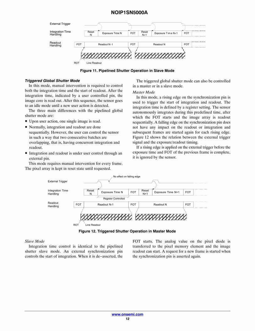
Master ModeIn this mode, a rising edge on the synchronization pin is
used to trigger the start of integration and readout. Theintegration time is defined by a register setting. The sensorautonomously integrates during this predefined time, afterwhich the FOT starts and the image array is readoutsequentially. A falling edge on the synchronization pin doesnot have any impact on the readout or integration andsubsequent frames are started again for each rising edge.Figure 12 shows the relation between the external triggersignal and the exposure/readout timing.
If a rising edge is applied on the external trigger before theexposure time and FOT of the previous frame is complete,it is ignored by the sensor.
Figure 12. Triggered Shutter Operation in Master Mode
Reset
NExposure Tim�e N
Reset
N+1Exposure Tim�e N�+1
Readout N�-1 FOTFOT Readout N
ÉÉÉÉÉÉÉÉÉÉÉÉÉÉÉÉÉÉÉÉÉÉÉÉÉÉÉÉÉÉÉÉÉÉÉÉÉÉ
ÉÉ
ÉÉÉÉ
FOT
Integration Tim�e
Handling
Readout
Handling
ÉÉÉÉÉÉÉÉÉÉÉÉÉÉÉÉÉÉÉÉÉÉÉÉÉÉÉÉÉÉÉÉÉÉÉÉÉÉ
ÉÉÉÉ
ÉÉROT Line Readout
External Trigger
No effect on falling edge
Register Controlled
FOT FOT
Slave ModeIntegration time control is identical to the pipelined
shutter slave mode. An external synchronization pincontrols the start of integration. When it is de−asserted, the
FOT starts. The analog value on the pixel diode istransferred to the pixel memory element and the imagereadout can start. A request for a new frame is started whenthe synchronization pin is asserted again.

NOIP1SN5000A
www.onsemi.com13
Non−Zero and Zero Row Overhead Time (ROT) ModesIn pipelined global shutter mode, the integration and
readout are done in parallel. Images are continuously readout and integration of frame N is ongoing during readout ofthe previous frame N−1. The readout of every frame startswith a Frame Overhead Time (FOT), during which theanalog value of the pixel diode is transferred to the pixelmemory element. After the FOT, the sensor is read out lineby line and the readout of each line is preceded by a RowOverhead Time (ROT) as shown in Figure 13.
In Reduced/Zero ROT operation mode (refer toFigure 14), the row blanking and kernel readout occur inparallel. This mode is called reduced ROT as a part of theROT is done while the image row is readout. The actual ROTcan thus be longer, however the perceived ROT will beshorter (‘overhead’ spent per line is reduced).
This operation mode can be used for two reasons:• Reduced total line time.
• Lower power due to reduced clock−rate.
Figure 13. Integration and Readout Sequence of the Sensor Operating in Pipelined Global Shutter Mode withNon−Zero ROT Readout.
ROTys
ROTys+1
ROTye
Readoutye
Valid Data
FOT( )Readout
ys
Readoutys
Figure 14. Integration and Readout Sequence of the Sensor operating in Pipelined Global Shutter Mode withZero ROT Readout.
ROTys
(blanked out)ROT
Readoutys+1
ys
ROT
Readoutye
ye−1ROT
Readoutdummy
ye
Valid Data
FOT( )

NOIP1SN5000A
www.onsemi.com14
SENSOR OPERATION
FlowchartFigure 15 shows the sensor operation flowchart. The sensor has six different ‘states’. Every state is indicated with the oval
circle. These states are Power off, Low power standby, Standby (1), Standby (2), Idle, Running.
Figure 15. Sensor Operation Flowchart
Power Up Sequence
Enable Clock Management - Part 2
(First Pass after Hard Reset)
Low-Power Standby
Required Register
Upload
Standby (2)
Soft Power-Up
Idle
Enable Sequencer
RunningSensor (re-)configuration
(optional)
Disable Sequencer
Soft Power-Down
Disable Clock ManagementPart 2
Power Off
Power DownSequence
Intermediate Standby
En
ab
le C
lock M
an
ag
em
en
t� -
Pa
rt� 2
(No
t F
irst
Pa
ss a
fte
r H
ard
Re
se
t)
Sensor (re-)configuration
(optional)
Sensor (re-)configuration
(optional)A
sse
rt�io
n o
f� re
se
t�_n
Pi�n
Enable Clock Management - Part 1
Poll Lock Indication
(only when PLL is enabled)
Disable Clock ManagementPart 1
Standby (1)
NOIP1SN5000A
www.onsemi.com15
Sensor States
Low Power StandbyIn low power standby state, all power supplies are on, but
internally every block is disabled. No internal clock isrunning (PLL / LVDS clock receiver is disabled).
All register settings are set to their default values (seeTable 37).
Only a subset of the SPI registers is active for read/writein order to be able to configure clock settings and leave thelow power standby state. The only SPI registers that shouldbe touched are the ones required for the ‘Enable ClockManagement’ action described in Enable ClockManagement − Part 1 on page 16
Standby (1)In standby state, the PLL/LVDS clock receiver is running,
but the derived logic clock signal is not enabled.
Standby (2)In standby state, the derived logic clock signal is running.
All SPI registers are active, meaning that all SPI registerscan be accessed for read or write operations. All other blocksare disabled.
IdleIn the idle state, all internal blocks are enabled, except the
sequencer block. The sensor is ready to start grabbingimages as soon as the sequencer block is enabled.
RunningIn running state, the sensor is enabled and grabbing
images. The sensor can be operated in global master/slavemodes.
User Actions: Power Up Functional Mode Sequences
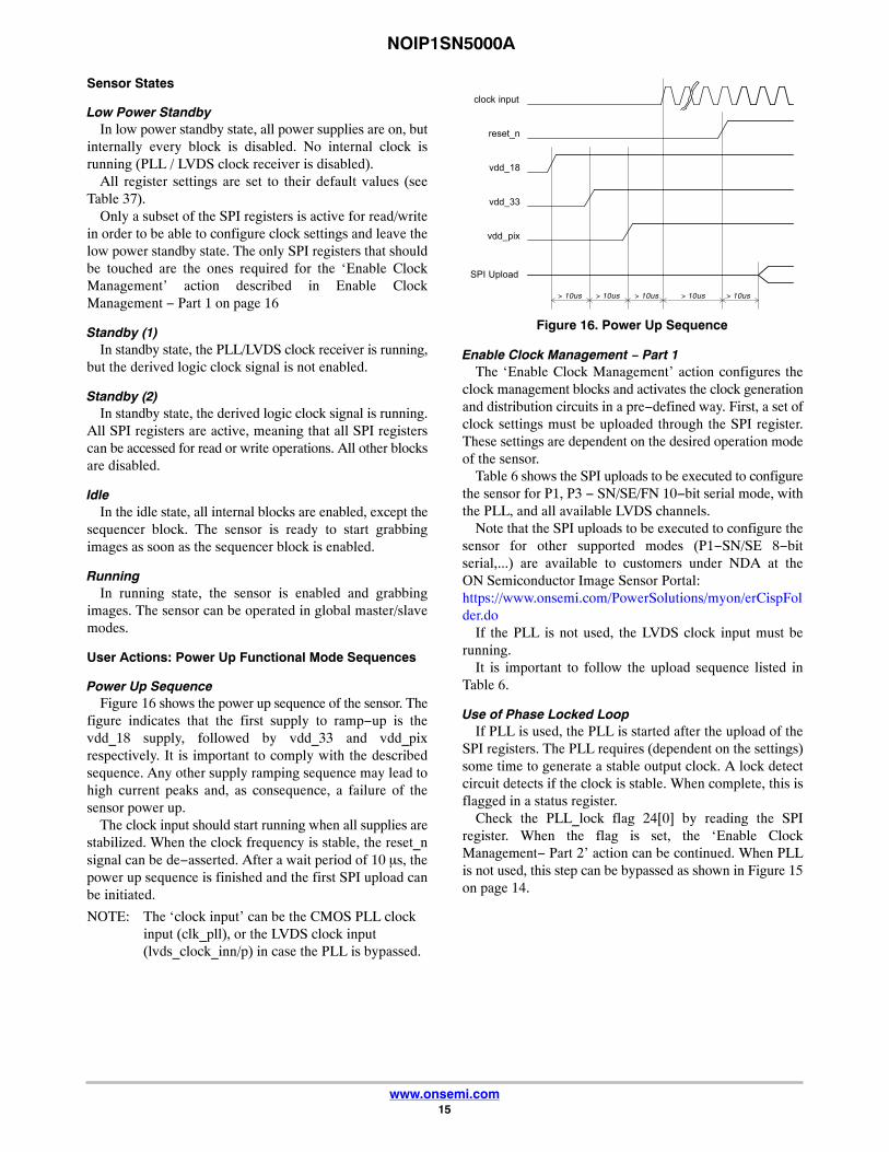
Power Up SequenceFigure 16 shows the power up sequence of the sensor. The
figure indicates that the first supply to ramp−up is thevdd_18 supply, followed by vdd_33 and vdd_pixrespectively. It is important to comply with the describedsequence. Any other supply ramping sequence may lead tohigh current peaks and, as consequence, a failure of thesensor power up.
The clock input should start running when all supplies arestabilized. When the clock frequency is stable, the reset_nsignal can be de−asserted. After a wait period of 10 �s, thepower up sequence is finished and the first SPI upload canbe initiated.
NOTE: The ‘clock input’ can be the CMOS PLL clockinput (clk_pll), or the LVDS clock input(lvds_clock_inn/p) in case the PLL is bypassed.
Figure 16. Power Up Sequence
reset_n
vdd_18
vdd_33
clock input
vdd_pix
> 10us> 10us> 10us > 10us
SPI Upload
> 10us
Enable Clock Management − Part 1The ‘Enable Clock Management’ action configures the
clock management blocks and activates the clock generationand distribution circuits in a pre−defined way. First, a set ofclock settings must be uploaded through the SPI register.These settings are dependent on the desired operation modeof the sensor.
Table 6 shows the SPI uploads to be executed to configurethe sensor for P1, P3 − SN/SE/FN 10−bit serial mode, withthe PLL, and all available LVDS channels.
Note that the SPI uploads to be executed to configure thesensor for other supported modes (P1−SN/SE 8−bitserial,...) are available to customers under NDA at theON Semiconductor Image Sensor Portal:https://www.onsemi.com/PowerSolutions/myon/erCispFolder.do
If the PLL is not used, the LVDS clock input must berunning.
It is important to follow the upload sequence listed inTable 6.
Use of Phase Locked LoopIf PLL is used, the PLL is started after the upload of the
SPI registers. The PLL requires (dependent on the settings)some time to generate a stable output clock. A lock detectcircuit detects if the clock is stable. When complete, this isflagged in a status register.
Check the PLL_lock flag 24[0] by reading the SPIregister. When the flag is set, the ‘Enable ClockManagement− Part 2’ action can be continued. When PLLis not used, this step can be bypassed as shown in Figure 15on page 14.

NOIP1SN5000A
www.onsemi.com16
Table 6. ENABLE CLOCK MANAGEMENT REGISTER UPLOAD − PART 1
Upload # Address Data Description
P1, P3 − SN/SE/FN 10−bit mode with PLL
1 2 0x0000 Monochrome sensor
0x0001 Color sensor
2 32 0x7004 Configure clock management P1 only
0x7014 Configure clock management P3 only
3 20 0x0000 Configure clock management
4 17 0x2113 Configure PLL
5 26 0x2280 Configure PLL lock detector
6 27 0x3D2D Configure PLL lock detector
7 8 0x0000 Release PLL soft reset
8 16 0x0003 Enable PLL
Enable Clock Management − Part 2The next step to configure the clock management consists
of SPI uploads which enables all internal clock distribution.The required uploads are listed in Table 7. Note that it isimportant to follow the upload sequence listed in Table 7.
Table 7. ENABLE CLOCK MANAGEMENT REGISTER UPLOAD − PART 2
Upload # Address Data Description
P1, P3 − SN/SE/FN 10−bit mode with PLL
1 9 0x0000 Release clock generator soft reset
2 32 0x7006 Enable logic clock for P1 only
0x7016 Enable logic clock for P3 only
3 34 0x0001 Enable logic block
Required Register UploadIn this phase, the ‘reserved’ register settings are uploaded
through the SPI register. Different settings are not allowedand may cause the sensor to malfunction. The requireduploads are listed in Table 8.
Table 8. REQUIRED REGISTER UPLOADS
Up-load #
Ad-dress
P1−SN/SE/FN 10−bitmode with PLL
(8 LVDS NZROT)
P3−SN/SE/FN 10−bitmode with PLL
(4 LVDS NZROT)
1 41 0x0854 0x0854
2 42 0x0200 0x0200
3 43 0x000C 0x000C
4 65 0x48CB 0x48CB
5 66 0x53C8 0x53C4
6 67 0x8688 0x4544
7 68 0x0085 0x0085
8 69 0x0888 0x0848
9 70 0x4411 0x4411
10 71 0x9788 0x9788
11 72 0x3330 0x3330
12 128 0x4714 0x4714
13 129 0x8001 0x8001
14 171 0x1002 0x1002
15 175 0x0080 0x0080
16 176 0x00E6 0x00E6
17 177 0x0400 0x0400
18 192 0x000C 0x000C
19 193 0x4E00 0x2C00
20 194 0x02E4 0x02E4
21 197 0x0104 0x0104
22 199 0x0196 0x0174
23 200 0x0804 0x0804
24 201 0x00B1 0x0060
25 204 0x01E1 0x01E1
26 207 0x0000 0x0000
27 208 0xA100 0xA100
28 211 0x0E49 0x0E39
29 215 0x111F 0x111F
30 216 0x7F00 0x7F00
31 219 0x0020 0x0020
32 220 0x2434 0x2432
33 224 0x3E17 0x3E17

NOIP1SN5000A
www.onsemi.com17
Up-load #
Ad-dress
P1−SN/SE/FN 10−bitmode with PLL
(8 LVDS NZROT)
P3−SN/SE/FN 10−bitmode with PLL
(4 LVDS NZROT)
34 227 0x0000 0x0000
35 250 0x2081 0x2081
36 256 0xA100 0xA100
37 257 0x0000 0x0000
38 258 0x07FF 0x07FF
39 384 0xC800 0xC800
40 385 0xFB1F 0xFB1F
41 386 0xFB1F 0xFB1F
42 387 0xFB12 0xFB12
43 388 0xF912 0xF912
44 389 0xF902 0xF902
45 390 0xF804 0xF804
46 391 0xF008 0xF008
47 392 0xF102 0xF102
48 393 0xF30F 0xF30F
49 394 0xF30F 0xF30F
50 395 0xF30F 0xF30F
51 396 0xF30F 0xF30F
52 397 0xF30F 0xF30F
53 398 0xF30F 0xF30F
54 399 0xF102 0xF102
55 400 0xF008 0xF008
56 401 0xF24A 0xF24A
57 402 0xF264 0xF264
58 403 0xF226 0xF226
59 404 0xF021 0xF021
60 405 0xF002 0xF002
61 406 0xF40A 0xF40A
62 407 0xF005 0xF005
63 408 0xF20F 0xF20F
64 409 0xF20F 0xF20F
65 410 0xF20F 0xF20F
66 411 0xF20F 0xF20F
67 412 0xF005 0xF005
68 413 0xEC05 0xEC05
69 414 0xC801 0xC801
70 415 0xC800 0xC800
Up-load #
Ad-dress
P1−SN/SE/FN 10−bitmode with PLL
(8 LVDS NZROT)
P3−SN/SE/FN 10−bitmode with PLL
(4 LVDS NZROT)
71 416 0xC800 0xC800
72 417 0xCC0A 0xCC0A
73 418 0xC806 0xC806
74 419 0xC800 0xC800
75 420 0x0030 0x0030
76 421 0x2179 0x2175
77 422 0x2071 0x2071
78 423 0x0071 0x0071
79 424 0x107F 0x107C
80 425 0x1079 0x0071
81 426 0x0071 0x0031
82 427 0x0031 0x01B2
83 428 0x01B4 0x21B5
84 429 0x21B9 0x20B1
85 430 0x20B1 0x00B1
86 431 0x00B1 0x10BC
87 432 0x10BF 0x00B1
88 433 0x10B9 0x0030
89 434 0x00B1 0x0030
90 435 0x0030 0x2075
91 436 0x0030 0x2071
92 437 0x2079 0x0071
93 438 0x2071 0x107C
94 439 0x0071 0x0071
95 440 0x107F 0x0031
96 441 0x1079 0x01B2
97 442 0x0071 0x21B5
98 443 0x0031 0x20B1
99 444 0x01B4 0x00B1
100 445 0x21B9 0x10BC
101 446 0x20B1 0x00B1
102 447 0x00B1 0x0030
103 448 0x10BF
104 449 0x10B9
105 450 0x00B1
106 451 0x0030
NOTE: Register uploads for other supported operation modes canbe accessed at the Image Sensor Portal on MyON.

NOIP1SN5000A
www.onsemi.com18
Soft Power UpDuring the soft power up action, the internal blocks are
enabled and prepared to start processing the image datastream. This action exists of a set of SPI uploads. The softpower up uploads are listed in Table 9.
Table 9. SOFT POWER UP REGISTER UPLOADS
Upload # Address Data Description
P1,P3 − SN/SE/FN 10−bit mode with PLL (P1 in ZROT, P3 in NZROT)
1 10 0x0000 Release soft reset state
2 32 0x7007 Enable analogue clock P1 only
0x7017 Enable analogue clock P3 only
3 64 0x0001 Enable biasing clock
4 40 0x0003 Enable column multiplexer
5 48 0x0001 Enable AFE
6 68 0x0085 Enable LVDS bias
7 72 0x3337 Enable charge pump
8 112 0x0007 Enable LVDS transmitters
Enable SequencerDuring the ‘Enable Sequencer’ action, the frame grabbing
sequencer is enabled. The sensor starts grabbing images inthe configured operation mode. Refer to Sensor States onpage 15.
The ‘Enable Sequencer’ action consists of a set of registeruploads. The required uploads are listed in Table 10.
Table 10. ENABLE SEQUENCER REGISTER UPLOADSUpload # Address Data
1 192 0x080D
User Actions: Functional Modes to Power Down Sequences
Disable SequencerDuring the ‘Disable Sequencer’ action, the frame
grabbing sequencer is stopped. The sensor stops grabbingimages and returns to the idle mode.
The ‘Disable Sequencer’ action consists of a set of registeruploads. as listed in Table 11.
Table 11. DISABLE SEQUENCER REGISTER UPLOADUpload # Address Data
1 192 0x080C
Soft Power DownDuring the soft power down action, the internal blocks are
disabled and the sensor is put in standby state to reduce thecurrent dissipation. This action exists of a set of SPI uploads.The soft power down uploads are listed in Table 12.
Table 12. SOFT POWER DOWN REGISTER UPLOADSUpload # Address Data Description
P1,P3 − SN/SE/FN 10−bit mode with PLL (P1 in ZROT, P3 in NZROT)
1 112 0x0000 Disable LVDS transmitters
2 72 0x3330 Disable charge pump
3 48 0x0000 Disable AFE
4 40 0x0000 Disable column multiplexer
5 64 0x0000 Disable biasing clock
6 32 0x7006 Disable analogue clock P1 only
0x7016 Disable analogue clock P3 only
7 10 0x0999 Soft reset

NOIP1SN5000A
www.onsemi.com19
Disable Clock Management − Part 2The ‘Disable Clock Management’ action stops the
internal clocking to further decrease the power dissipation.This action can be implemented with the SPI uploads asshown in Table 13.
Table 13. DISABLE CLOCK MANAGEMENT REGISTER UPLOAD − PART 2
Upload # Address Data Description
P1,P3 − SN/SE/FN 10−bit mode with PLL
1 32 0x7004 Disable logic clock P1 only
0x7014 Disable logic clock P3 only
2 34 0x0000 Disable logic blocks
3 9 0x0009 Soft reset clock generator
Disable Clock Management − Part 1The ‘Disable Clock Management’ action stops the
internal clocking to further decrease the power dissipation.This action can be implemented with the SPI uploads asshown in Table 14.
Table 14. DISABLE CLOCK MANAGEMENT REGISTER UPLOAD − PART 1
Upload # Address Data Description
P1,P3 − SN/SE/FN 10−bit mode with PLL
1 8 0x0099 Soft reset PLL
2 16 0x0000 Disable PLL
Power Down SequenceFigure 17 illustrates the timing diagram of the preferred
power down sequence. It is important that the sensor is inreset before the clock input stops running. Otherwise, theinternal PLL becomes unstable and the sensor gets into anunknown state. This can cause high peak currents.
The same applies for the ramp down of the powersupplies. The preferred order to ramp down the supplies isfirst vdd_pix, second vdd_33, and finally vdd_18. Any othersequence can cause high peak currents.
NOTE: The ‘clock input’ can be the CMOS PLL clockinput (clk_pll), or the LVDS clock input(lvds_clock_inn/p) in case the PLL is bypassed.
Figure 17. Power Down Sequence
reset_n
vdd_18
vdd_33
clock input
vdd_pix
> 10us > 10us> 10us > 10us

NOIP1SN5000A
www.onsemi.com20
Sensor reconfigurationDuring the standby, idle, or running state several sensor
parameters can be reconfigured.• Frame Rate and Exposure Time: Frame rate and
exposure time changes can occur during standby, idle,and running states by modifying registers 199 to 203.Refer to page 30−32 for more information.
• Signal Path Gain: Signal path gain changes can occurduring standby, idle, and running states by modifyingregisters 204/205. Refer to page 37 for moreinformation.
• Windowing: Changes with respect to windowing canoccur during standby, idle, and running states. Refer toMultiple Window Readout on page 28 for moreinformation.
• Subsampling: Changes of the subsampling mode canoccur during standby, idle, and running states bymodifying register 192. Refer to Subsampling onpage 29 for more information.
• Shutter Mode: The shutter mode can only be changedduring standby or idle mode by modifying register 192.Reconfiguring the shutter mode during running state isnot supported.
Sensor ConfigurationThis device contains multiple configuration registers.
Some of these registers can only be configured while thesensor is not acquiring images (while register 192[0] = 0),while others can be configured while the sensor is acquiringimages. For the latter category of registers, it is possible todistinguish the register set that can cause corrupted images(limited number of images containing visible artifacts) fromthe set of registers that are not causing corrupted images.
These three categories are described here.
Static Readout ParametersSome registers are only modified when the sensor is not
acquiring images. reconfiguration of these registers whileimages are acquired can cause corrupted frames or eveninterrupt the image acquisition. Therefore, it isrecommended to modify these static configurations whilethe sequencer is disabled (register 192[0] = 0). The registersshown in Table 15 should not be reconfigured during imageacquisition. A specific configuration sequence applies forthese registers. Refer to the operation flow and startupdescription.
Table 15. STATIC READOUT PARAMETERS
Group Addresses Description
Clock generator 32 Configure according to recommendation
Image core 40 Configure according to recommendation
AFE 48 Configure according to recommendation
Bias 64–71 Configure according to recommendation
Charge Pump 72 Configure according to recommendation
LVDS 112 Configure according to recommendation
Sequencer mode selection 192 [6:1] Operation modes are: • triggered_mode
• slave_mode
All reserved registers Keep reserved registers to their default state, unless otherwise described in the recommendation
Dynamic Configuration Potentially Causing ImageArtifacts
The category of registers as shown in Table 16 consists ofconfigurations that do not interrupt the image acquisitionprocess, but may lead to one or more corrupted imagesduring and after the reconfiguration. A corrupted image is an
image containing visible artifacts. A typical example of acorrupted image is an image which is not uniformlyexposed.
The effect is transient in nature and the new configurationis applied after the transient effect.
Table 16. DYNAMIC CONFIGURATION POTENTIALLY CAUSING IMAGE ARTIFACTS
Group Addresses Description
Black level configuration 128–129
197[12:8]
Reconfiguration of these registers may have an impact on the black−level calibration algorithm. The effect is a transient number of images with incorrect black level com-pensation.
Sync codes 129[13]
116–126
Incorrect sync codes may be generated during the frame in which these registers are modified.
Datablock test configurations 144, 146–150 Modification of these registers may generate incorrect test patterns during a transient frame.
NOIP1SN5000A
www.onsemi.com21
Dynamic Readout ParametersIt is possible to reconfigure the sensor while it is acquiring
images. Frame related parameters are internallyresynchronized to frame boundaries, such that the modifiedparameter does not affect a frame that has already started.However, there can be restrictions to some registers as
shown in Table 17. Some reconfiguration may lead to oneframe being blanked. This happens when the modificationrequires more than one frame to settle. The image is blankedout and training patterns are transmitted on the data and syncchannels.
Table 17. DYNAMIC READOUT PARAMETERS
Group Addresses Description
Subsampling/binning 192[7]
192[8]
Subsampling or binning is synchronized to a new frame start.
ROI configuration 195
256–303
A ROI switch is only detected when a new window is selected as the active window (reconfiguration of register 195). reconfiguration of the ROI dimension of the active window does notlead to a frame blank and can cause a corrupted image.
Exposure reconfiguration
199−203 Exposure reconfiguration does not cause artifact. However, a latency of one frame is observed unlessreg_seq_exposure_sync_mode is set to ‘1’ in triggered global mode (master).
Gain reconfiguration 204 Gains are synchronized at the start of a new frame. Optionally, one frame latency can be incorporatedto align the gain updates to the exposure updates (refer to register 204[13] − gain_lat_comp).
Freezing Active ConfigurationsThough the readout parameters are synchronized to frame
boundaries, an update of multiple registers can still lead toa transient effect in the subsequent images, as someconfigurations require multiple register uploads. Forexample, to reconfigure the exposure time in master globalmode, both the fr_length and exposure registers need to beupdated. Internally, the sensor synchronizes theseconfigurations to frame boundaries, but it is still possiblethat the reconfiguration of multiple registers spans over twoor even more frames. To avoid inconsistent combinations,freeze the active settings while altering the SPI registers bydisabling synchronization for the correspondingfunctionality before reconfiguration. When all registers areuploaded, re−enable the synchronization. The sensor’ssequencer then updates its active set of registers and uses
them for the coming frames. The freezing of the active setof registers can be programmed in the sync_configurationregisters, which can be found at the SPI address 206.
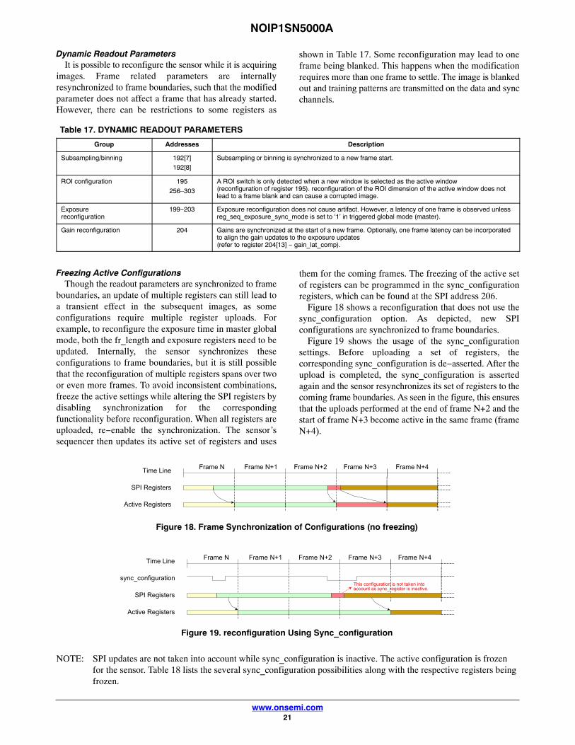
Figure 18 shows a reconfiguration that does not use thesync_configuration option. As depicted, new SPIconfigurations are synchronized to frame boundaries.
Figure 19 shows the usage of the sync_configurationsettings. Before uploading a set of registers, thecorresponding sync_configuration is de−asserted. After theupload is completed, the sync_configuration is assertedagain and the sensor resynchronizes its set of registers to thecoming frame boundaries. As seen in the figure, this ensuresthat the uploads performed at the end of frame N+2 and thestart of frame N+3 become active in the same frame (frameN+4).
Figure 18. Frame Synchronization of Configurations (no freezing)
Frame N���Frame N+1�� Frame N+2�� �Frame N+3 Frame N+4Time Line
SPI Registers
Active Registers
Figure 19. reconfiguration Using Sync_configuration
Frame N���Frame N+1�� Frame N+2�� �Frame N+3�� �Frame N+4Time Line
sync_configuration
SPI Registers
Active Registers
This configuration is not taken into account as sync_register is inactive.
NOTE: SPI updates are not taken into account while sync_configuration is inactive. The active configuration is frozenfor the sensor. Table 18 lists the several sync_configuration possibilities along with the respective registers beingfrozen.

NOIP1SN5000A
www.onsemi.com22
Table 18. ALTERNATE SYNC CONFIGURATIONS
Group Affected Registers Description
sync_black_lines black_lines Update of black line configuration is not synchronized at start of frame when ‘0’. The sensor continues with its previous configurations.
sync_exposure mult_timer
fr_length
exposure
Update of exposure configurations is not synchronized at start of frame when ‘0’. The sensor continues with its previous configurations.
sync_gain mux_gainsw
afe_gain
Update of gain configurations is not synchronized at start of frame when ‘0’. The sensor continues with its previous configurations.
sync_roi roi_active0[15:0]
subsampling
binning
Update of active ROI configurations is not synchronized at start of frame when ‘0’. The sensor continues with its previous configurations.
Note: The window configurations themselves are not frozen. reconfiguration of active windows is not gated by this setting.
Window Configuration
Global Shutter ModeUp to 16 windows can be defined in global shutter mode
(pipelined or triggered). The windows are defined byregisters 256 to 303. Each window can be activated ordeactivated separately using register 195. It is possible toreconfigure the inactive windows while the sensor isacquiring images.
Switching between predefined windows is achieved byactivation of the respective windows. This way a minimumnumber of registers need to be uploaded when it is necessaryto switch between two or more sets of windows. As anexample of this, scanning the scene at higher frame ratesusing multiple windows and switching to full frame capturewhen the object is tracked. Switching between the twomodes only requires an upload of one register.
Black CalibrationThe sensor automatically calibrates the black level for
each frame. Therefore, the device generates a configurablenumber of electrical black lines at the start of each frame.The desired black level in the resulting output interface canbe configured and is not necessarily targeted to ‘0’.Configuring the target to a higher level yields someinformation on the left side of the black level distribution,while the other end of the distribution tail is clipped to ‘0’when setting the black level target to ‘0’.
The black level is calibrated for the 16 columns containedin one kernel. This implies 16 black level offsets aregenerated and applied to the corresponding columns.Configurable parameters for the black−level algorithm arelisted in Table 19.
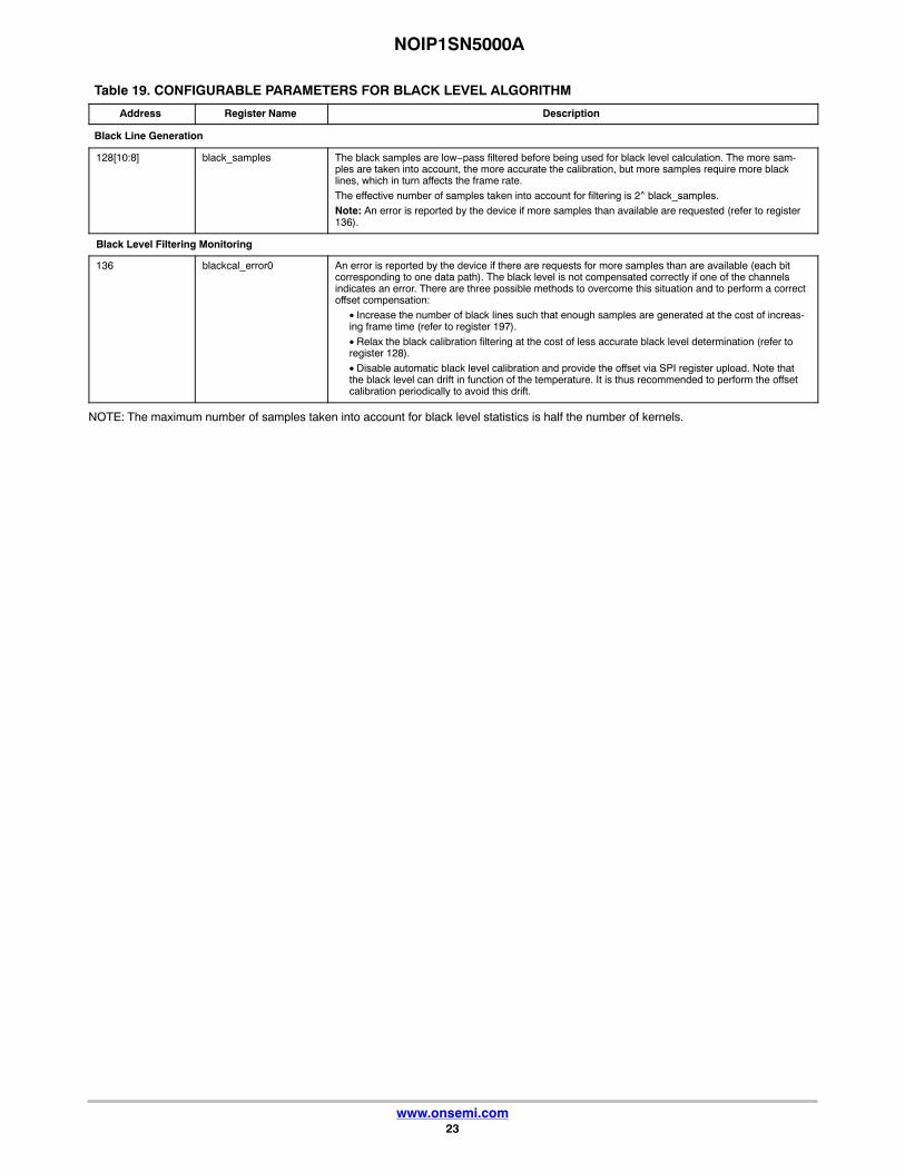
Table 19. CONFIGURABLE PARAMETERS FOR BLACK LEVEL ALGORITHM
Address Register Name Description
Black Line Generation
197[7:0] black_lines This register configures the number of black lines that are generated at the start of a frame. At least oneblack line must be generated. The maximum number is 255.
Note: When the automatic black−level calibration algorithm is enabled, make sure that this register isconfigured properly to produce sufficient black pixels for the black−level filtering.
The number of black pixels generated per line is dependent on the operation mode and window configu-rations:
Each black line contains 162 kernels.
197[12:8] gate_first_line A number of black lines are blanked out when a value different from 0 is configured. These blanked outlines are not used for black calibration. It is recommended to enable this functionality, because the firstline can have a different behavior caused by boundary effects. When enabling, the number of blacklines must be set to at least two in order to have valid black samples for the calibration algorithm.
Black Value Filtering
129[0] auto_blackcal_enable Internal black−level calibration functionality is enabled when set to ‘1’. Required black level offset com-pensation is calculated on the black samples and applied to all image pixels.
When set to ‘0’, the automatic black−level calibration functionality is disabled. It is possible to apply anoffset compensation to the image pixels, which is defined by the registers 129[10:1].
Note: Black sample pixels are not compensated; the raw data is sent out to provide external statistics and, optionally, calibrations.
129[9:1] blackcal_offset Black calibration offset that is added or subtracted to each regular pixel value when auto_blackcal_en-able is set to ‘0’. The sign of the offset is determined by register 129[10] (blackcal_offset_dec).
Note: All channels use the same offset compensation when automatic black calibration is disabled.
129[10] blackcal_offset_dec Sign of blackcal_offset. If set to ‘0’, the black calibration offset is added to each pixel. If set to ‘1’, theblack calibration offset is subtracted from each pixel.
This register is not used when auto_blackcal_enable is set to ‘1’.
NOIP1SN5000A
www.onsemi.com23
Table 19. CONFIGURABLE PARAMETERS FOR BLACK LEVEL ALGORITHM
Address DescriptionRegister Name
Black Line Generation
128[10:8] black_samples The black samples are low−pass filtered before being used for black level calculation. The more sam-ples are taken into account, the more accurate the calibration, but more samples require more blacklines, which in turn affects the frame rate.
The effective number of samples taken into account for filtering is 2^ black_samples.
Note: An error is reported by the device if more samples than available are requested (refer to register136).
Black Level Filtering Monitoring
136 blackcal_error0 An error is reported by the device if there are requests for more samples than are available (each bitcorresponding to one data path). The black level is not compensated correctly if one of the channelsindicates an error. There are three possible methods to overcome this situation and to perform a correctoffset compensation:
• Increase the number of black lines such that enough samples are generated at the cost of increas-ing frame time (refer to register 197).
• Relax the black calibration filtering at the cost of less accurate black level determination (refer toregister 128).
• Disable automatic black level calibration and provide the offset via SPI register upload. Note thatthe black level can drift in function of the temperature. It is thus recommended to perform the offsetcalibration periodically to avoid this drift.
NOTE: The maximum number of samples taken into account for black level statistics is half the number of kernels.
NOIP1SN5000A
www.onsemi.com24
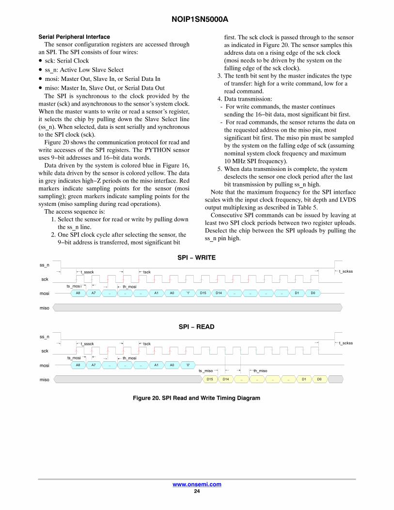
Serial Peripheral InterfaceThe sensor configuration registers are accessed through
an SPI. The SPI consists of four wires:• sck: Serial Clock
• ss_n: Active Low Slave Select
• mosi: Master Out, Slave In, or Serial Data In
• miso: Master In, Slave Out, or Serial Data OutThe SPI is synchronous to the clock provided by the
master (sck) and asynchronous to the sensor’s system clock.When the master wants to write or read a sensor’s register,it selects the chip by pulling down the Slave Select line(ss_n). When selected, data is sent serially and synchronousto the SPI clock (sck).
Figure 20 shows the communication protocol for read andwrite accesses of the SPI registers. The PYTHON sensoruses 9−bit addresses and 16−bit data words.
Data driven by the system is colored blue in Figure 16,while data driven by the sensor is colored yellow. The datain grey indicates high−Z periods on the miso interface. Redmarkers indicate sampling points for the sensor (mosisampling); green markers indicate sampling points for thesystem (miso sampling during read operations).
The access sequence is:1. Select the sensor for read or write by pulling down
the ss_n line.2. One SPI clock cycle after selecting the sensor, the
9−bit address is transferred, most significant bit
first. The sck clock is passed through to the sensoras indicated in Figure 20. The sensor samples thisaddress data on a rising edge of the sck clock(mosi needs to be driven by the system on thefalling edge of the sck clock).
3. The tenth bit sent by the master indicates the typeof transfer: high for a write command, low for aread command.
4. Data transmission:- For write commands, the master continues
sending the 16−bit data, most significant bit first.- For read commands, the sensor returns the data on
the requested address on the miso pin, mostsignificant bit first. The miso pin must be sampledby the system on the falling edge of sck (assumingnominal system clock frequency and maximum10 MHz SPI frequency).
5. When data transmission is complete, the systemdeselects the sensor one clock period after the lastbit transmission by pulling ss_n high.
Note that the maximum frequency for the SPI interfacescales with the input clock frequency, bit depth and LVDSoutput multiplexing as described in Table 5.
Consecutive SPI commands can be issued by leaving atleast two SPI clock periods between two register uploads.Deselect the chip between the SPI uploads by pulling thess_n pin high.
Figure 20. SPI Read and Write Timing Diagram
.. A1 A0 `1'A8 D1�5 D14 .. .. .. .. D1 D0
sck
mosi
ss_n
miso
A7 .. ..
.. A1 A0 `0'A8
sck
mosi
ss_n
miso
A7 .. ..
D1�5 D14 .. .. .. .. D1 D0
ts_mosi th_mosi
t_sssck t_sckss
ts _miso th_miso
t_scksst_sssck
ts _mos i th_mosi
tsck
tsck
SPI − WRITE
SPI − READ
NOIP1SN5000A
www.onsemi.com25
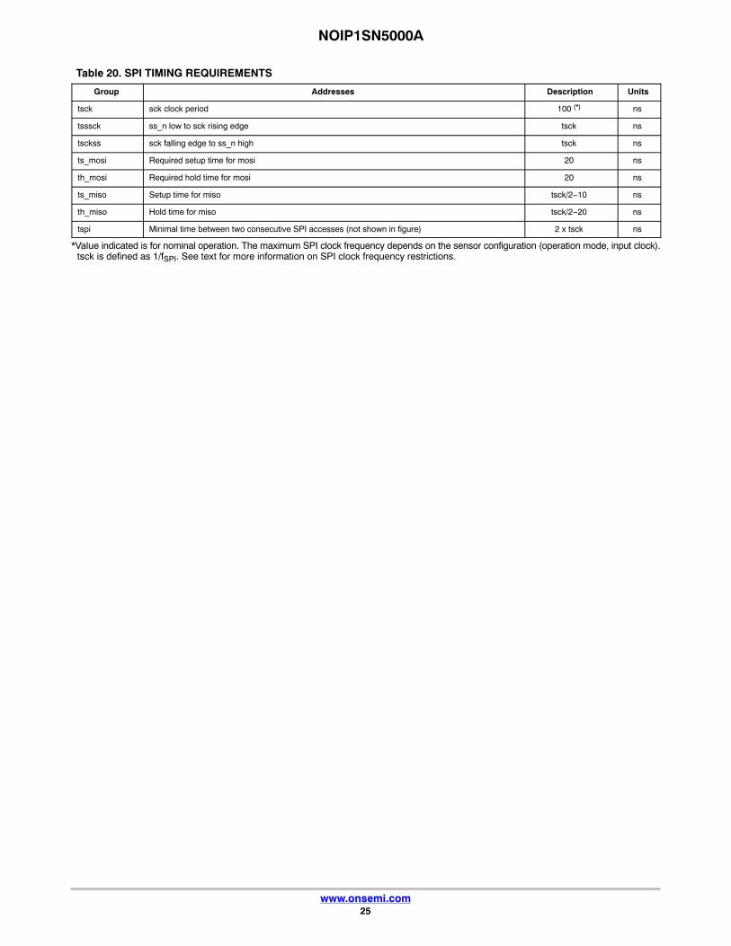
Table 20. SPI TIMING REQUIREMENTS
Group Addresses Description Units
tsck sck clock period 100 (*) ns
tsssck ss_n low to sck rising edge tsck ns
tsckss sck falling edge to ss_n high tsck ns
ts_mosi Required setup time for mosi 20 ns
th_mosi Required hold time for mosi 20 ns
ts_miso Setup time for miso tsck/2−10 ns
th_miso Hold time for miso tsck/2−20 ns
tspi Minimal time between two consecutive SPI accesses (not shown in figure) 2 x tsck ns
*Value indicated is for nominal operation. The maximum SPI clock frequency depends on the sensor configuration (operation mode, input clock).tsck is defined as 1/fSPI. See text for more information on SPI clock frequency restrictions.
NOIP1SN5000A
www.onsemi.com26
IMAGE SENSOR TIMING AND READOUT
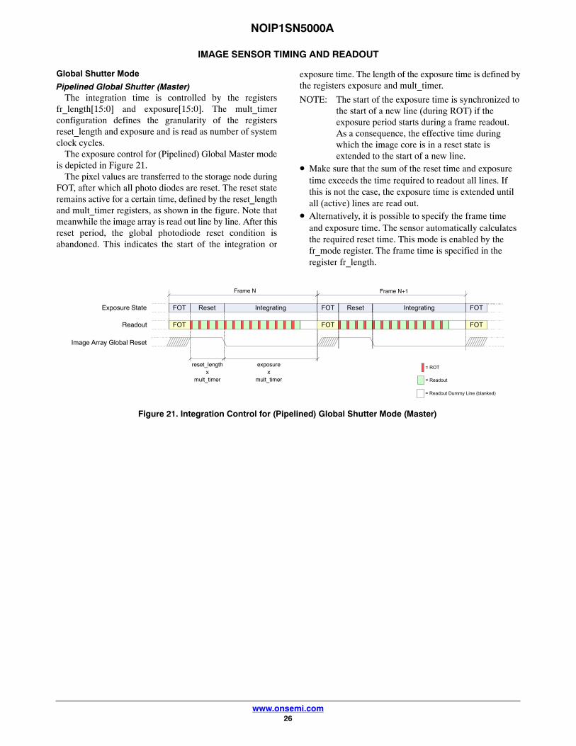
Global Shutter Mode
Pipelined Global Shutter (Master)The integration time is controlled by the registers
fr_length[15:0] and exposure[15:0]. The mult_timerconfiguration defines the granularity of the registersreset_length and exposure and is read as number of systemclock cycles.
The exposure control for (Pipelined) Global Master modeis depicted in Figure 21.
The pixel values are transferred to the storage node duringFOT, after which all photo diodes are reset. The reset stateremains active for a certain time, defined by the reset_lengthand mult_timer registers, as shown in the figure. Note thatmeanwhile the image array is read out line by line. After thisreset period, the global photodiode reset condition isabandoned. This indicates the start of the integration or
exposure time. The length of the exposure time is defined bythe registers exposure and mult_timer.
NOTE: The start of the exposure time is synchronized tothe start of a new line (during ROT) if theexposure period starts during a frame readout.As a consequence, the effective time duringwhich the image core is in a reset state isextended to the start of a new line.
• Make sure that the sum of the reset time and exposuretime exceeds the time required to readout all lines. Ifthis is not the case, the exposure time is extended untilall (active) lines are read out.
• Alternatively, it is possible to specify the frame timeand exposure time. The sensor automatically calculatesthe required reset time. This mode is enabled by thefr_mode register. The frame time is specified in theregister fr_length.
Figure 21. Integration Control for (Pipelined) Global Shutter Mode (Master)
Reset Integrating Reset Integrating
Image Array Global Reset
Readout
FOT
FOT FOT
FOT
FOT
FOT
reset_lengthx
mult_timer
Frame N Frame N+1
Exposure State
= ROT
= Readout
= Readout Dummy Line (blanked)
exposurex
mult_timer

NOIP1SN5000A
www.onsemi.com27
Triggered Global Shutter (Master)In master triggered global mode, the start of integration
time is controlled by a rising edge on the trigger0 pin. Theexposure or integration time is defined by the registers
exposure and mult_timer, as in the master pipelined globalmode. The fr_length configuration is not used. Thisoperation is graphically shown in Figure 22.
Figure 22. Exposure Time Control in Triggered Shutter Mode (Master)
Reset Integrating Reset Integrating
Image Array Global Reset
Readout
FOT
FOT FOT
FOT
FOT
FOT
exposure x mult_timer
Frame N Frame N+1
Exposure State
(No effect on falling edge)trigger0
= ROT
= Readout
= Readout Dummy Line (blanked)
Notes:• The falling edge on the trigger pin does not have any
impact. Note however the trigger must be asserted forat least 100 ns.
• The start of the exposure time is synchronized to thestart of a new line (during ROT) if the exposure periodstarts during a frame readout. As a consequence, theeffective time during which the image core is in a resetstate is extended to the start of a new line.
• If the exposure timer expires before the end of readout,the exposure time is extended until the end of the lastactive line.
• The trigger pin needs to be kept low during the FOT.The monitor pins can be used as a feedback to theFPGA/controller (eg. use monitor0, indicating the veryfirst line when monitor_select = 0x5 − a new trigger canbe initiated after a rising edge on monitor0).
Triggered Global Shutter (Slave)Exposure or integration time is fully controlled by means
of the trigger pin in slave mode. The registers fr_length,exposure and mult_timer are ignored by the sensor.
A rising edge on the trigger pin indicates the start of theexposure time, while a falling edge initiates the transfer to
the pixel storage node and readout of the image array. Inother words, the high time of the trigger pin indicates theintegration time, the period of the trigger pin indicates theframe time.
The use of the trigger during slave mode is shown inFigure 23.
Notes:• The registers exposure, fr_length, and mult_timer are
not used in this mode.• The start of exposure time is synchronized to the start
of a new line (during ROT) if the exposure period startsduring a frame readout. As a consequence, the effectivetime during which the image core is in a reset state isextended to the start of a new line.
• If the trigger is de−asserted before the end of readout,the exposure time is extended until the end of the lastactive line.
• The trigger pin needs to be kept low during the FOT.The monitor pins can be used as a feedback to theFPGA/controller (eg. use monitor0, indicating the veryfirst line when monitor_select = 0x5 − a new trigger canbe initiated after a rising edge on monitor0).
Figure 23. Exposure Time Control in Global−Slave Mode
Reset Integrating Reset Integrating
Image Array Global Reset
Readout
FOT
FOT FOT
FOT
FOT
FOT
Frame N Frame N+1
Exposure State
trigger0
= ROT
= Readout
= Readout Dummy Line (blanked)

NOIP1SN5000A
www.onsemi.com28
ADDITIONAL FEATURES
Multiple Window ReadoutThe PYTHON 2000 and PYTHON 5000 sensor supports
multiple window readout, which means that only theuser−selected Regions Of Interest (ROI) are read out. Thisallows limiting data output for every frame, which in turnallows increasing the frame rate. In global shutter mode, upto eight ROIs can be configured.
Window ConfigurationFigure 24 shows the four parameters defining a region of
interest (ROI).
Figure 24. Region of Interest Configuration
y-start
y-end
x-start���������� x-end
ROI 0
• x−start[7:0]x−start defines the x−starting point of the desired window.
The sensor reads out 16 pixels in one single clock cycle. Asa consequence, the granularity for configuring the x−startposition is also 16 pixels for no sub sampling. The valueconfigured in the x−start register is multiplied by 16 to findthe corresponding column in the pixel array.• x−end[7:0]
This register defines the window end point on the x−axis.Similar to x−start, the granularity for this configuration isone kernel. x−end needs to be larger than x−start.• y−start[9:0]
The starting line of the readout window. The granularityof this setting is one line, except with color sensors where itneeds to be an even number.• y−end[9:0]
The end line of the readout window. y−end must beconfigured larger than y−start. This setting has the samegranularity as the y−start configuration.
Up to eight windows can be defined, possibly (partially)overlapping, as illustrated in Figure 25.
Figure 25. Overlapping Multiple WindowConfiguration
y0_start
y1_start
y0_end
y1_end
x0_start
x1_start
x0_end
x1_end
ROI 0
ROI 1
The sequencer analyses each line that needs to be read outfor multiple windows.
RestrictionsThe following restrictions for each line are assumed for
the user configuration:• Windows are ordered from left to right, based on their
x−start address:
x_start_roi(i) x_start_roi(j) AND�
x_end_roi(i) x_end_roi(j)�
Where j i>
Processing Multiple WindowsThe sequencer control block houses two sets of counters
to construct the image frame. As previously described, they−counter indicates the line that needs to be read out and isincremented at the end of each line. For the start of the frame,it is initialized to the y−start address of the first window andit runs until the y−end address of the last window to be readout. The last window is configured by the configurationregisters and it is not necessarily window #15.
The x−counter starts counting from the x−start address ofthe window with the lowest ID which is active on theaddressed line. Only windows for which the currenty−address is enclosed are taken into account for scanning.Other windows are skipped.
Figure 26 illustrates a practical example of aconfiguration with five windows. The current position of theread pointer (ys) is indicated by a red line crossing the image
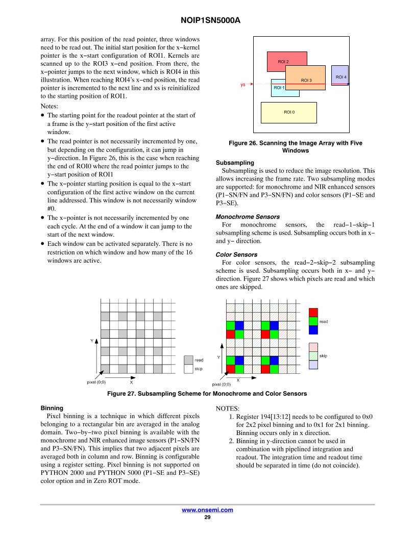
NOIP1SN5000A
www.onsemi.com29
array. For this position of the read pointer, three windowsneed to be read out. The initial start position for the x−kernelpointer is the x−start configuration of ROI1. Kernels arescanned up to the ROI3 x−end position. From there, thex−pointer jumps to the next window, which is ROI4 in thisillustration. When reaching ROI4’s x−end position, the readpointer is incremented to the next line and xs is reinitializedto the starting position of ROI1.
Notes:• The starting point for the readout pointer at the start of
a frame is the y−start position of the first activewindow.
• The read pointer is not necessarily incremented by one,but depending on the configuration, it can jump iny−direction. In Figure 26, this is the case when reachingthe end of ROI0 where the read pointer jumps to they−start position of ROI1
• The x−pointer starting position is equal to the x−startconfiguration of the first active window on the currentline addressed. This window is not necessarily window#0.
• The x−pointer is not necessarily incremented by oneeach cycle. At the end of a window it can jump to thestart of the next window.
• Each window can be activated separately. There is norestriction on which window and how many of the 16windows are active.
Figure 26. Scanning the Image Array with FiveWindows
ROI 0
ROI 1
ROI 4
ysROI 3
ROI 2
SubsamplingSubsampling is used to reduce the image resolution. This
allows increasing the frame rate. Two subsampling modesare supported: for monochrome and NIR enhanced sensors(P1−SN/FN and P3−SN/FN) and color sensors (P1−SE andP3−SE).
Monochrome SensorsFor monochrome sensors, the read−1−skip−1
subsampling scheme is used. Subsampling occurs both in x−and y− direction.
Color SensorsFor color sensors, the read−2−skip−2 subsampling
scheme is used. Subsampling occurs both in x− and y−direction. Figure 27 shows which pixels are read and whichones are skipped.
Figure 27. Subsampling Scheme for Monochrome and Color Sensors
BinningPixel binning is a technique in which different pixels
belonging to a rectangular bin are averaged in the analogdomain. Two−by−two pixel binning is available with themonochrome and NIR enhanced image sensors (P1−SN/FNand P3−SN/FN). This implies that two adjacent pixels areaveraged both in column and row. Binning is configurableusing a register setting. Pixel binning is not supported onPYTHON 2000 and PYTHON 5000 (P1−SE and P3−SE)color option and in Zero ROT mode.
NOTES:1. Register 194[13:12] needs to be configured to 0x0
for 2x2 pixel binning and to 0x1 for 2x1 binning.Binning occurs only in x direction.
2. Binning in y-direction cannot be used incombination with pipelined integration andreadout. The integration time and readout timeshould be separated in time (do not coincide).

NOIP1SN5000A
www.onsemi.com30
Reverse Readout in Y−directionReverse readout in y−direction can be done by asserting
reverse_y (reg 194[8]). The reference for y_start and y_stoppointers is reversed.
Channel MultiplexingThe PYTHON 2000 and PYTHON 5000 image sensors
contains a function for channel multiplexing the output
channels. Using this function, one may for instance use thedevice with sync+clock+8 data channels. Enabling thechannel multiplexing is done through register 32[5:4]. Thedefault value of 0 disables all channel multiplexing. Highervalues sets higher degree of channel multiplexing. Thechannels that are used per degree of multiplexing are shownin Table 5. The unused data channels are powered down andwill not send any data.
Table 21. LVDS DATA OUTPUT CHANNELS USED WITH CHANNEL MULTIPLEXING
# outputs PYTHON 2000 / PYTHON 5000 − LVDS ChannelsRegister 32[5:4]
DataRegister 211
Data
8 channels Ch 0 Ch 1 Ch 2 Ch 3 Ch 4 Ch 5 Ch 6 Ch 7 0 0x0E49
4 channels Ch 0 Ch 2 Ch 4 Ch 6 1 0x0E39
2 channels Ch 0 Ch 2 2 0x0E29
1 channel Ch 0 3 0x0E19
1. P1 supports 8 LVDS channels, while P1, P3 support 4, 2 and 1 channels.2. Use P3 bias uploads for P1 when operating in mux mode.
Table 22. BIAS UPLOADS FOR P1 AND P3
Bias Uploads Address mux 8:8 mux 8:4 mux 8:2 mux 8:1
reg_mux_image_core_config1 41 0x0854 0x0854 0x0854 0x0854
reg_mux_image_core_config2 42 0x0203 0x0203 0x0203 0x0203
reg_mux_image_core_config3 43 0x000C 0x000C 0x000C 0x000C
reg_bias_configuration 65 0x48CB 0x48CB 0x48CB 0x48CB
reg_bias_afe_bias 66 0x53C8 0x53C4 0x53C2 0x53C1
reg_bias_mux_bias 67 0x8688 0x4544 0x2322 0x1211
reg_bias_lvds_bias 68 0x0085 0x0085 0x0085 0x0085
reg_bias_adc_bias 69 0x0888 0x0848 0x0828 0x0818
reg_bias_imc_bias 70 0x4411 0x4411 0x4411 0x4411
reg_cp_configuration 72 0x3337 0x3337 0x3337 0x3337

NOIP1SN5000A
www.onsemi.com31
Multiple Slope Integration‘Multiple Slope Integration’ is a method to increase the
dynamic range of the sensor. The PYTHON supports up tothree slopes.
Figure 28 shows the sensor response to light when thesensor is used with one slope, two slopes, and three slopes.The X−axis represents the light power; the Y−axis shows thesensor output signal. The kneepoint of the multiple slopecurves are adjustable in both position and voltage level.
It is clear that when using only one slope (red curve), thesensor has the same responsivity over the entire range, untilthe output saturates at the point indicated with ‘single slopesaturation point’.
To increase the dynamic range of the sensor, a secondslope is applied in the dual slope mode (green curve). Thesensor has the same responsivity in the black as for a singleslope, but from ‘knee point 1’ on, the sensor is lessresponsive to incoming light. The result is that the saturationpoint is at a higher light power level.
To further increase the dynamic range, a third slope can beapplied, resulting in a second knee point.
Refer to section Global Shutter Mode on page 26 forgeneral notes applicable to the global shutter operation andmore particular to the use of the trigger0 pin.
Figure 28. Multiple Slope Operation
slope 1���� slope 2
slope 3
light
output
1023
0
`kneepoint 1'
`kneepoint 2'
single slope
saturation pointdual slope
saturation point
triple slope
saturation point
Kneepoint Configuration (Multiple Slope Reset Levels)The kneepoint reset levels are configured by means of
DAC configurations in the image core. The dual slopekneepoint is configured with the dac_ds configuration,while the triple slope kneepoint is configured with thedac_ts register setting. Both are located on address 41.
Multiple Slope Integration in “Master Mode” (Pipelinedor Triggered)
In master mode, the time stamps for the double and tripleslope resets are configured in a similar way as the exposuretime. They are enabled through the registers
dual_slope_enable and triple_slope_enable and their valuesare defined by the registers exposure_ds and exposure_ts.
NOTE: Dual and triple slope sequences must start afterreadout of the previous frame is fully completed.
Figure 29 shows the frame timing for pipelined mastermode with dual and triple slope integration andfr_mode = ‘0’ (fr_length representing the reset length).
In triggered master mode, the start of integration isinitiated by a rising edge on trigger0, while the falling edgedoes not have any relevance. Exposure duration anddual/triple slope points are defined by the registers.

NOIP1SN5000A
www.onsemi.com32
Figure 29. Multiple Slope Operation in Master Mode for fr_mode = ‘0’ (Pipelined)
Slave ModeIn slave mode, the register settings for integration control
are ignored. The user has full control through the trigger0,trigger1 and trigger2 pins. A falling edge on trigger1initiates the dual slope reset while a falling edge on trigger2
initiates the triple slope reset sequence. Rising edges ontrigger1 and trigger2 do not have any impact.
NOTE: Dual and triple slope sequences must start afterreadout of the previous frame is fully completed.
Figure 30. Multiple Slope Operation in Slave Mode
Black ReferenceThe sensor reads out one or more black lines at the start of
every new frame. The number of black lines to be generatedis programmable and is minimal equal to 1. The length of theblack lines depends on the operation mode. The sensoralways reads out the entire line (162 kernels), independentof window configurations.
The black references are used to perform black calibrationand offset compensation in the data channels. The raw black
pixel data is transmitted over the usual output interface,while the regular image data is compensated (can bebypassed).
On the output interface, black lines can be seen as aseparate window, however without Frame Start and Ends(only Line Start/End). The Sync code following the LineStart and Line End indications (“window ID”) contains theactive window number, which is 0. Black reference data isclassified by a BL code.

NOIP1SN5000A
www.onsemi.com33
Signal Path Gain
Analog Gain StagesReferring to Table 23, several gain settings are available
in the analog data path to apply gain to the analog signalbefore it is digitized.
The moment a gain reconfiguration is applied andbecomes valid can be controlled by the gain_lat_compconfiguration.
With ‘gain_lat_comp’ set to ‘0’, the new gainconfigurations are applied from the very next frame.
With ‘gain_lat_comp’ set to ‘1’, the new gain settings arepostponed by one extra frame. This feature is useful whenexposure time and gain are reconfigured together, as anexposure time update always has one frame latency.
Table 23. SIGNAL PATH GAIN STAGES
Address Gain SettingAnalog Gain Non−Zero
and Zero ROT
204[12:0] 0x01E1 1
204[12:0] 0x00A1 1.6
204[12:0] 0x0021 2
204[12:0] 0x0083 2.6
204[12:0] 0x0085 3.2
204[12:0] 0x0081 4
204[12:0] 0x0086 5.3
204[12:0] 0x0082 8
NOTE: Analog gain above 2x affects the noise performance.
Digital Gain StageThe digital gain stage allows fine gain adjustments on the
digitized samples. The gain configuration is an absolute 5.7unsigned number (5 digits before and 7 digits after thedecimal point).

NOIP1SN5000A
www.onsemi.com34
Automatic Exposure ControlThe exposure control mechanism has the shape of a
general feedback control system. Figure 31 shows the highlevel block diagram of the exposure control loop.
Figure 31. Automatic Exposure Control Loop
AECStatistics
AECFilter
AECEnforcer
Req
uest
ed G
ain
Cha
nges
Tota
l Gai
n
Integration TimeAnalog Gain (Coarse Steps)
Requested Illumination Level(Target)
Digital Gain (Fine Steps)
Image Capture
Three main blocks can be distinguished:• The statistics block compares the average of the
current image’s samples to the configured target valuefor the average illumination of all pixels
• The relative gain change request from the statisticsblock is filtered through the AEC Filter block in thetime domain (low pass filter) before being integrated.The output of the filter is the total requested gain in thecomplete signal path.
• The enforcer block accepts the total requested gain anddistributes this gain over the integration time and gainstages (both analog and digital)
The automatic exposure control loop is enabled byasserting the aec_enable configuration in register 160.
NOTE: Dual and Triple slope integration is notsupported in conjunction with the AEC.
AEC Statistics BlockThe statistics block calculates the average illumination of
the current image. Based on the difference between the
calculated illumination and the target illumination thestatistics block requests a relative gain change.
Statistics Subsampling and WindowingFor average calculation, the statistics block will
sub−sample the current image or windows by taking everyfourth sample into account. Note that only the pixels read outthrough the active windows are visible for the AEC. In thecase where multiple windows are active, the samples will beselected from the total samples. Samples contained in aregion covered by multiple (overlapping) window will betaking into account only once.
It is possible to define an AEC specific sub−window onwhich the AEC will calculate it’s average. For instance, thesensor can be configured to read out a larger frame, while theillumination is measured on a smaller region of interest, e.g.center weighted as shown in Table 24.
Table 24. AEC SAMPLE SELECTION
Register Name Description
192[10] roi_aec_enable When 0x0, all active windows are selected for statistics calculation.When 0x1, the AEC samples are selected from the active pixels contained in the region of interest defined by roi_aec
253−255 roi_aec These registers define a window from which the AEC samples will be selected when roi_aec_enable is asserted. Configuration is similar to the regular region of interests.The intersection of this window with the active windows define the selected pixels. It is important that this window at leastoverlaps with one or more active windows.
NOIP1SN5000A
www.onsemi.com35
Target IlluminationThe target illumination value is configured by means of
register desired_intensity as shown in Table 25.
Table 25. AEC TARGET ILLUMINATIONCONFIGURATION
Register Name Description
161[9:0] desired_in-tensity
Target intensity value, on 10−bit scale.For 8−bit mode, target value is configuredon desired_intensity[9:2]
Color SensorThe weight of each color can be configured for color
sensors by means of scale factors. Note these scale factor areonly used to calculate the statistics in order to compensatefor (off−chip) white balancing and/or color matrices. Thepixel values itself are not modified.
The scale factors are configured as 3.7 unsigned numbers(0x80 = unity). Refer to Table 26 for color scale factors. Formono sensors, configure these factors to their default value.
Table 26. COLOR SCALE FACTORS
Register Name Description
162[9:0] red_scale_factor Red scale factor for AEC statistics
163[9:0] green1_scale_factor Green1 scale factor for AECstatistics
164[9:0] green2_scale_factor Green2 scale factor for AECstatistics
165[9:0] blue_scale_factor Blue scale factor for AEC statistics
AEC Filter BlockThe filter block low−pass filters the gain change requests
received from the statistics block.The filter can be restarted by asserting the restart_filter
configuration of register 160.
AEC Enforcer BlockThe enforcer block calculates the four different gain
parameters, based on the required total gain, therebyrespecting a specific hierarchy in those configurations.Some (digital) hysteresis is added so that the (analog) sensorsettings don’t need to change too often.
Exposure Control ParametersThe several gain parameters are described below, in the
order in which these are controlled by the AEC for largeadjustments. Small adjustments are regulated by digital gainonly.• Exposure Time
The exposure is the time between the global image arrayreset de−assertion and the pixel charge transfer. Thegranularity of the integration time steps is configured by themult_timer register.
NOTE: The exposure_time register is ignored when theAEC is enabled. The register fr_length definesthe frame time and needs to be configuredaccordingly.
• Analog GainThe sensor has two analog gain settings. Typically the
AEC shall only regulate the first stage.• Digital Gain
The last gain stage is a gain applied on the digitizedsamples. The digital gain is represented by a 5.7 unsignednumber (i.e. 7 bits after the decimal point). While the analoggain steps are coarse, the digital gain stage makes it possibleto achieve very fine adjustments.

NOIP1SN5000A
www.onsemi.com36
AEC Control RangeThe control range for each of the exposure parameters can
be pre−programmed in the sensor. Table 27 lists the relevantregisters.
Table 27. MINIMUM AND MAXIMUM EXPOSURECONTROL PARAMETERS
Register Name Description
168[15:0] min_exposure Lower bound for the integration timeapplied by the AEC
169[1:0] min_mux_gain Lower bound for the first stage analog amplifier. This stage has two configurations with the following approximative gains:0x0 = 1x0x1 = 2x
169[3:2] min_afe_gain Lower bound for the second stageanalog amplifier.This stage has only one configuration with the following approximative gain:0x0 = 1.00x
169[15:4] min_digital_gain Lower bound for the digital gainstage. This configuration specifies the effective gain in 5.7 unsigned format
170[15:0] max_exposure Upper bound for the integration timeapplied by the AEC
171[1:0] max_mux_gain Upper bound for the first stage ana-log amplifier.This stage has two configurations with the following approximative gains:0x0 = 1x0x1 = 2x
171[3:2] max_afe_gain Upper bound for the second stageanalog amplifier
This stage has only one configuration with the following approximative gain:0x0 = 1.00x
171[15:4] max_digital_gain
Upper bound for the digital gainstage. This configuration specifies the effective gain in 5.7 unsigned format
AEC Update FrequencyAs an integration time update has a latency of one frame,
the exposure control parameters are evaluated and updatedevery other frame.
Note: The gain update latency must be postpone to matchthe integration time latency. This is done by asserting thegain_lat_comp register on address 204[13].
Exposure Control Status RegistersConfigured integration and gain parameters are reported
to the user by means of status registers. The sensor providestwo levels of reporting: the status registers reported in theAEC address space are updated once the parameters arerecalculated and requested to the internal sequencer. Thestatus registers residing in the sequencer’s address space onthe other hand are updated once these parameters are takingeffect on the image readout. Refer to Table 28 reflecting theAEC and Sequencer Status registers.
Table 28. EXPOSURE CONTROL STATUS REGISTERS
Register Name Description
AEC Status Registers
184[15:0] total_pixels Total number of pixels taken into accountfor the AEC statistics.
186[9:0] average Calculated average illumination level for the current frame.
187[15:0] exposure AEC calculated exposure.Note: this parameter is updated at theframe end.
188[1:0] mux_gain AEC calculated analog gain (1st stage)Note: this parameter is updated at theframe end.
188[3:2] afe_gain AEC calculated analog gain (2st stage)Note: this parameter is updated at theframe end.
188[15:4] digital_gain AEC calculated digital gain (5.7 unsigned format)Note: this parameter is updated at theframe end.

NOIP1SN5000A
www.onsemi.com37
Table 28. EXPOSURE CONTROL STATUS REGISTERS
Register Name Description
Sequencer Status Registers
242[15:0] mult_timer mult_timer for current frameNote: this parameter is updated once ittakes effect on the image.
243[15:0] reset_length Image array reset length for the current frame.Note: this parameter is updated once ittakes effect on the image.
244[15:0] exposure Exposure for the current frame.Note: this parameter is updated once ittakes effect on the image.
245[15:0] exposure_ds Dual slope exposure for the currentframe. Note this parameter is not con-trolled by the AEC.Note: this parameter is updated once ittakes effect on the image.
246[15:0] exposure_ts Triple slope exposure for the current frame. Note this parameter is notcontrolled by the AEC.Note: this parameter is updated once ittakes effect on the image.
247[4:0] mux_gainsw 1st stage analog gain for the currentframe.Note: this parameter is updated once ittakes effect on the image.
247[12:5] afe_gain 2st stage analog gain for the currentframe.Note: this parameter is updated once ittakes effect on the image.
248[11:0] db_gain Digital gain configuration for the currentframe (5.7 unsigned format).Note: this parameter is updated once ittakes effect on the image.
248[12] dual_slope Dual slope configuration for the current frameNote 1: this parameter is updated once ittakes effect on the image.Note 2: This parameter is not controlled by the AEC.
248[13] triple_slope Triple slope configuration for the currentframe.Note 1: this parameter is updated once ittakes effect on the image.Note 2: This parameter is not controlled by the AEC.

NOIP1SN5000A
www.onsemi.com38
Mode Changes and Frame BlankingDynamically reconfiguring the sensor may lead to
corrupted or non-uniformilly exposed frames. For somereconfigurations, the sensor automatically blanks out theimage data during one frame. Frame blanking is
summarized in the following table for the sensor’s imagerelated modes.
NOTE: Major mode switching (i.e. switching betweenmaster, triggered or slave mode) must beperformed while the sequencer is disabled(reg_seq_enable = 0x0).
Table 29. DYNAMIC SENSOR RECONFIGURATION AND FRAME BLANKING
ConfigurationCorrupted
FrameBlanked Out
Frame Notes
Shutter Mode and Operation
triggered_mode Do not reconfigure while the sensor is acquiring images. Disable image acquisition by setting reg_seq_enable = 0x0.
slave_mode Do not reconfigure while the sensor is acquiring images. Disable image acquisition by setting reg_seq_enable = 0x0.
subsampling Enabling: NoDisabling: Yes
Configurable Configurable with blank_subsampling_ss register.
binning No Configurable Configurable with blank_subsampling_ss register
Frame Timing
black_lines No No
Exposure Control
mult_timer No No Latency is 1 frame
fr_length No No Latency is 1 frame
exposure No No Latency is 1 frame
Gain
mux_gainsw No No Latency configurable by means of gain_lat_comp register
afe_gain No No Latency configurable by means of gain_lat_comp register.
db_gain No No Latency configurable by means of gain_lat_comp register.
Window/ROI
roi_active See Note No Windows containing lines previously not read out may lead to corruptedframes.
roi*_configuration* See Note No Reconfiguring the windows by means of roi*_configuration* may lead tocorrupted frames when configured close to frame boundaries. It is recommended to (re)configure an inactive window and switch theroi_active register.See Notes on roi_active.
Black Calibration
black_samples No No If configured within range of configured black lines
auto_blackal_enable See Note No Manual correction factors become instantly active when auto_blackcal_enable is deasserted during operation.
blackcal_offset See Note No Manual blackcal_offset updates are instantly active.
CRC Calculation
crc_seed No No Impacts the transmitted CRC
Sync Channel
bl_0 No No Impacts the Sync channel information, not the Data channels.
img_0 No No Impacts the Sync channel information, not the Data channels.
crc_0 No No Impacts the Sync channel information, not the Data channels.
tr_0 No No Impacts the Sync channel information, not the Data channels.

NOIP1SN5000A
www.onsemi.com39
Temperature SensorThe PYTHON has an on−chip temperature sensor which
returns a digital code (Tsensor) of the silicon junctiontemperature. The Tsensor output is a 8−bit digital countbetween 0 and 255, proportional to the temperature of thesilicon substrate. This reading can be translated directly toa temperature reading in °C by calibrating the 8−bit readoutat 0°C and 85°C to achieve an output accuracy of ±2°C. TheTsensor output can also be calibrated using a singletemperature point (example: room temperature or theambient temperature of the application), to achieve anoutput accuracy of ±5°C.
Note that any process variation will result in an offset inthe bit count and that offset will remain within ±5°C over thetemperature range of 0°C and 85°C. Tsensor output digitalcode can be read out through the SPI interface.
Output of the temperature sensor to the SPI:tempd_reg_temp<7:0>: This is the 8−bit N count readout
proportional to temperature.
Input from the SPI:The reg_tempd_enable is a global enable and this enables
or disables the temperature sensor when logic high or logiclow respectively. The temperature sensor is reset or disabledwhen the input reg_tempd_enable is set to a digital low state.
Calibration using one temperature pointThe temperature sensor resolution is fixed for a given type
of package for the operating range of 0°C to +85°C andhence devices can be calibrated at any ambient temperatureof the application, with the device configured in the mode ofoperation.
Interpreting the actual temperature for the digital codereadout:
The formula used isTJ = R (Nread − Ncalib) + TcalibTJ = junction die temperatureR = resolution in degrees/LSB (typical 0.75 deg/LSB)Nread = Tsensor output (LSB count between 0 and 255)Tcalib = Tsensor calibration temperatureNcalib = Tsensor output reading at Tcalib
Monitor PinsThe internal sequencer has two monitor outputs (monitor0
and monitor1) that can be used to communicate the internalstates from the sequencer. A three−bit register configures theassignment of the pins as shown in Table 30.
Table 30. REGISTER SETTING FOR THE MONITOR SELECT PIN
monitor_select [2:0]
192 [13:11] monitor pin Description
0x0 monitor0
monitor1
‘0’
‘0’
0x1 monitor0
monitor1
Integration Time
ROT Indication (‘1’ during ROT, ‘0’ outside)
0x2 monitor0
monitor1
Integration Time
Dual/Triple Slope Integration (asserted during DS/TS FOT sequence)
0x3 monitor0
monitor1
Start of x−Readout Indication
Black Line Indication (‘1’ during black lines, ‘0’ outside)
0x4 monitor0
monitor1
Frame Start Indication
Start of ROT Indication
0x5 monitor0
monitor1
First Line Indication (‘1’ during first line, ‘0’ for all others)
Start of ROT Indication
0x6 monitor0
monitor1
ROT Indication (‘1’ during ROT, ‘0’ outside)
Start of X−Readout Indication
0x7 monitor0
monitor1
Start of X−readout Indication for Black Lines
Start of X−readout Indication for Image Lines

NOIP1SN5000A
www.onsemi.com40
DATA OUTPUT FORMAT
The PYTHON 2000 and PYTHON 5000 image sensorsare available in two LVDS output configuration, P1 and P3.The P1 configuration utilizes eight LVDS output channelstogether with an LVDS clock output and an LVDSsynchronization output channel. The P3 configurationconsists of four LVDS output channels together with anLVDS clock output and an LVDS synchronization outputchannel.
P1,P3−SN/SE/FN: Interface Version
LVDS Output ChannelsThe image data output occurs through eight LVDS data
channels where a synchronization LVDS channel and anLVDS output clock signal synchronizes the data.
Referring to Table 21, the eight data channels on the P1option are used to output the image data only, while on theP3 option, four data channel channels are utilized. The syncchannel transmits information about the data sent over thesedata channels (includes codes indicating black pixels,normal pixels, and CRC codes).
8−bit / 10−bit ModeThe sensor can be used in 8−bit or 10−bit mode.In 10−bit mode, the words on data and sync channel have
a 10−bit length. The output data rate is 720 Mbps.In 8−bit mode, the words on data and sync channel have
an 8−bit length, the output data rate is 576 Mbps.Note that the 8−bit mode can only be used to limit the data
rate at the consequence of image data word depth. It is notsupported to operate the sensor in 8−bit mode at a higherclock frequency to achieve higher frame rates. The P1 optionsupports 10−bit/8−bit in ZROT/NZROT mode, while the P3option supports 10−bit NZROT mode only.
Frame FormatThe frame format in 8−bit mode is identical to the 10−bit
mode with the exception that the Sync and data word depthis reduced to eight bits.
The frame format in 10−bit mode is explained by exampleof the readout of two (overlapping) windows as shown inFigure 32(a).
The readout of a frame occurs on a line−by−line basis. Theread pointer goes from left to right, bottom to top.
Figure 32 indicates that, after the FOT is completed, thesensor reads out a number of black lines for black calibrationpurposes. After these black lines, the windows areprocessed. First a number of lines which only includesinformation of ‘ROI 0’ are sent out, starting at positiony0_start. When the line at position y1_start is reached, anumber of lines containing data of ‘ROI 0’ and ‘ROI 1’ aresent out, until the line position of y0_end is reached. Fromthere on, only data of ‘ROI 1’ appears on the data outputchannels until line position y1_end is reached
During read out of the image data over the data channels,the sync channel sends out frame synchronization codeswhich give information related to the image data that is sentover the four data output channels.
Each line of a window starts with a Line Start (LS)indication and ends with a Line End (LE) indication. Theline start of the first line is replaced by a Frame Start (FS);the line end of the last line is replaced with a Frame Endindication (FE). Each such frame synchronization code isfollowed by a window ID (range 0 to 7). For overlappingwindows, the line synchronization codes of the overlappingwindows with lower IDs are not sent out (as shown in theillustration: no LE/FE is transmitted for the overlapping partof window 0).
NOTES: In Figure 32, only Frame Start and Frame EndSync words are indicated in (b). CRC codes arealso omitted from the figure.
For additional information on thesynchronization codes, please refer to PYTHONImage Sensor Family Developer’s GuideAND9362/D.

NOIP1SN5000A
www.onsemi.com41
Figure 32. P1&P3−SN/SE/FN: Frame Sync Codes
(a)
(b)
y0_start
y1_start
y0_end
y1_end
x0_start
x1_start
x0_end
x1_end
ROI 0
Reset
NExposure Time N
Reset
N+1Exposure Time N+1
ROI 0 FOT FOT
Integration Time
Handling
Readout
HandlingFOT
ROI
1
Readout Frame N-1 Readout Frame N
ROI 0ROI
1
FS0 FS1 FE1 FS0 FS1 FE1
ÉÉ
B
L
ÉÉ
B
L
FOT FOT
ROI 1
Figure 33 shows the detail of a black line readout during global or full−frame readout.
Figure 33. P1&P3−SN/SE/FN: Time Line for Black Line Readout
data channels
sync channel
data channels
sync channel
SequencerInternal State
line Ys line Ys+1 line Yeblack
timeslot
0
Training
TR LS BL LE
Training
TR
FOT ROT ROT ROTROT
CRCBL BL BL BL BL
timeslot
1
timeslot
157
timeslot
158
timeslot
159
CRC
timeslot

NOIP1SN5000A
www.onsemi.com42
Figure 34 shows the details of the readout of a number of lines for single window readout, at the beginning of the frame.
Figure 34. P1&P3−SN/SE/FN: Time Line for Single Window Readout (at the start of a frame)
data channels
sync channel
data channels
sync channel
Sequencer
Internal Stateline Ys line Ys+1 line Yeblack
timeslot
Xstart
Training
TR FS ID IMG LE
Training
TR
FOT ROT ROT ROT
ID
ROT
CRCIMG IMG IMG IMG IMG
timeslot
Xstart + 1
timeslot
Xend - 2
timeslot
Xend - 1
timeslot
Xend
CRC
timeslot
Figure 35 shows the detail of the readout of a number of lines for readout of two overlapping windows.
Figure 35. P1&P3−SN/SE/FN: Time Line Showing the Readout of Two Overlapping Windows
data channels
sync channel
data channels
sync channel
Sequencer
Internal Stateline Ys+1 line Yeblack
timeslot
XstartM
Training
TR LS IDM IMG LE
Training
TR
FOT ROT ROT ROT
IDN
ROT
CRCIMG LS IDN IMG IMG
timeslot
XstartN
timeslot
XendN
line Ys
IMG
Frame Synchronization for 10−bit ModeTable 31 shows the structure of the frame synchronization
code. Note that the table shows the default data word(configurable) for 10−bit mode. If more than one window is
active at the same time, the sync channel transmits the framesynchronization codes of the window with highest indexonly.
Table 31. FRAME SYNCHRONIZATION CODE DETAILS FOR 10−BIT MODE
Sync Word BitPosition
RegisterAddress Default Value Description
9:7 N/A 0x5 Frame start (FS) indication
9:7 N/A 0x6 Frame end (FE) indication
9:7 N/A 0x1 Line start (LS) indication
9:7 N/A 0x2 Line end (LE) indication
6:0 117[6:0] 0x2A These bits indicate that the received sync word is a frame synchronization code. The value is pro-grammable by a register setting
Window IdentificationFrame synchronization codes are always followed by a
4−bit window identification (bits 3:0). This is an integer
number, ranging from 0 to 15, indicating the active window.If more than one window is active for the current cycle, thehighest window ID is transmitted.

NOIP1SN5000A
www.onsemi.com43
Data Classification CodesFor the remaining cycles, the sync channel indicates the
type of data sent through the data links: black pixel data
(BL), image data (IMG), or training pattern (TR). Thesecodes are programmable by a register setting. The defaultvalues are listed in Table 32.
Table 32. SYNCHRONIZATION CHANNEL DEFAULT IDENTIFICATION CODE VALUES FOR 10−BIT MODE
Sync Word BitPosition
Register Ad-dress
Default Val-ue Description
9:0 118 [9:0] 0x015 Black pixel data (BL). This data is not part of the image. The black pixel data is used internally to correct channel offsets.
9:0 119 [9:0] 0x035 Valid pixel data (IMG). The data on the data output channels is valid pixel data (part of the image).
9:0 125 [9:0] 0x059 CRC value. The data on the data output channels is the CRC code of the finished image data line.
9:0 126 [9:0] 0x3A6 Training pattern (TR). The sync channel sends out the training pattern which can be programmed by a register setting.
Frame Synchronization in 8−bit ModeThe frame synchronization words are configured using
the same registers as in 10−bit mode. The two leastsignificant bits of these configuration registers are ignored
and not sent out. Table 32 shows the structure of the framesynchronization code, together with the default value, asspecified in SPI registers. The same restriction foroverlapping windows applies in 8−bit mode.
Table 33. FRAME SYNCHRONIZATION CODE DETAILS FOR 8−BIT MODE
Sync Word BitPosition
Register Ad-dress
Default Val-ue Description
7:5 N/A 0x5 Frame start (FS) indication
7:5 N/A 0x6 Frame end (FE) indication
7:5 N/A 0x1 Line start (LS) indication
7:5 N/A 0x2 Line end (LE) indication
4:0 117 [6:2] 0x0A These bits indicate that the received sync word is a frame synchronization code. The value is programmable by a register setting.
Window IdentificationSimilar to 10−bit operation mode, the frame
synchronization codes are followed by a windowidentification. The window ID is located in bits 5:2 (all otherbit positions are ‘0’). The same restriction for overlappingwindows applies in 8−bit mode.
Data Classification CodesBL, IMG, CRC, and TR codes are defined by the same
registers as in 10−bit mode. Bits 9:2 of the respectiveconfiguration registers are used as classification code withdefault values shown in Table 34.
Table 34. SYNCHRONIZATION CHANNEL DEFAULT IDENTIFICATION CODE VALUES FOR 8−BIT MODE
Sync Word BitPosition
Register Ad-dress
Default Val-ue Description
7:0 118 [9:2] 0x05 Black pixel data (BL). This data is not part of the image. The black pixel data is used internally to correct channel offsets.
7:0 119 [9:2] 0x0D Valid pixel data (IMG). The data on the data output channels is valid pixel data (part of the image).
7:0 125 [9:2] 0x16 CRC value. The data on the data output channels is the CRC code of the finished image data line.
7:0 126 [9:2] 0xE9 Training Pattern (TR). The sync channel sends out the training pattern which can be programmed by a register setting.
NOIP1SN5000A
www.onsemi.com44
Training Patterns on Data ChannelsIn 10−bit mode, during idle periods, the data channels
transmit training patterns, indicated on the sync channel bya TR code. These training patterns are configurable
independent of the training code on the sync channel asshown in Table 35.
Table 35. TRAINING CODE ON SYNC CHANNEL IN 10−BIT MODE
Sync Word BitPosition
Register Ad-dress
DefaultValue Description
[9:0] 116 [9:0] 0x3A6 Data channel training pattern. The data output channels send out the training pattern, which can beprogrammed by a register setting. The default value of the training pattern is 0x3A6, which is identicalto the training pattern indication code on the sync channel.
In 8−bit mode, the training pattern for the data channels isdefined by the same register as in 10−bit mode, where thelower two bits are omitted; see Table 36.
Table 36. TRAINING PATTERN ON DATA CHANNEL IN 8−BIT MODE
Data Word BitPosition
Register Ad-dress
DefaultValue Description
[7:0] 116 [9:2] 0xE9 Data Channel Training Pattern (Training pattern).
Cyclic Redundancy CodeAt the end of each line, a CRC code is calculated to allow
error detection at the receiving end. Each data channeltransmits a CRC code to protect the data words sent duringthe previous cycles. Idle and training patterns are notincluded in the calculation.
The sync channel is not protected. A special character(CRC indication) is transmitted whenever the data channelssend their respective CRC code.
The polynomial in 10−bit operation mode isx10 + x9 + x6 + x3 + x2 + x + 1. The CRC encoder is seeded
at the start of a new line and updated for every (valid) dataword received. The CRC seed is configurable using thecrc_seed register. When ‘0’, the CRC is seeded by all−‘0’;when ‘1’ it is seeded with all−‘1’.
In 8−bit mode, the polynomial is x8 + x6 + x3 + x2 + 1.The CRC seed is configured by means of the crc_seedregister.
NOTE: The CRC is calculated for every line. Thisimplies that the CRC code can protect lines frommultiple windows.

NOIP1SN5000A
www.onsemi.com45
Data Order for P1&P3−SN/SE/FNTo read out the image data through the output channels,
the pixel array is organized in kernels. The kernel size issixteen pixels in x−direction by one pixel in y−direction. Thedata order in 8−bit mode is identical to the 10−bit mode.
Figure 36 indicates how the kernels are organized. The firstkernel (kernel [0, 0]) is located in the bottom left corner(front view on top of the package). The data order of thisimage data on the data output channels depends on thesubsampling mode.
Figure 36. Kernel Organization in Pixel Array − Top View
ROI
kernel(0,0)
kernel(161,2047)
kernel(x_start,y_start)
0 15321 13 14
pixel array
• P1&P3−SN/SE/FN: Subsampling Disabled♦ 8 LVDS Output Channels (P1 only)
The image data is read out in kernels of 16 pixels inx−direction by one pixel in y−direction. One data channeloutput delivers two pixel values of one kernel sequentially.
Figure 37 shows how a kernel is read out over the eightoutput channels. For even positioned kernels, the kernels areread out ascending, while for odd positioned kernels the dataorder is reversed (descending).
Figure 37. P1−SN/SE/FN: 8 LVDS Data Output Order when Subsampling is Disabled
kernel N−2 kernel N+1kernel Nkernel N−1
0 4321 11 15141312pixel # (even kernel)
chan
nel #
0
chan
nel #
1
chan
nel #
7
chan
nel #
6
15 11121314 4 0123pixel # (odd kernel)
10−bit 10−bit
MSB LSB MSB LSB
Note: The bit order is always MSB first
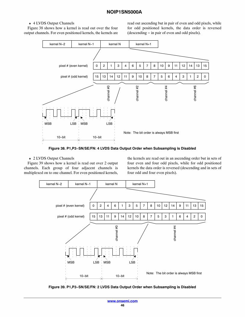
NOIP1SN5000A
www.onsemi.com46
♦ 4 LVDS Output ChannelsFigure 38 shows how a kernel is read out over the four
output channels. For even positioned kernels, the kernels are
read out ascending but in pair of even and odd pixels, whilefor odd positioned kernels, the data order is reversed(descending − in pair of even and odd pixels).
Figure 38. P1,P3−SN/SE/FN: 4 LVDS Data Output Order when Subsampling is Disabled
kernel N−2 kernel N+1kernel Nkernel N−1
0 4312 1412119pixel # (even kernel)
chan
nel #
0
15 11121413 1346pixel # (odd kernel)
10−bit 10−bit
MSB LSB MSB LSB
Note: The bit order is always MSB first
6 10875
9 57810
1513
02
chan
nel #
2
chan
nel #
4
chan
nel #
6
♦ 2 LVDS Output ChannelsFigure 39 shows how a kernel is read out over 2 output
channels. Each group of four adjacent channels ismultiplexed on to one channel. For even positioned kernels,
the kernels are read out in an ascending order but in sets offour even and four odd pixels, while for odd positionedkernels the data order is reversed (descending and in sets offour odd and four even pixels).
Figure 39. P1,P3−SN/SE/FN: 2 LVDS Data Output Order when Subsampling is Disabled
kernel N−2 kernel N+1kernel Nkernel N−1
0 1642 1191412pixel # (even kernel)
chan
nel #
0
15 1491113 4613pixel # (odd kernel)
10−bit 10−bit
MSB LSB MSB LSB
Note: The bit order is always MSB first
3 10875
12 57810
1513
02
chan
nel #
4

NOIP1SN5000A
www.onsemi.com47
♦ 1 LVDS Output ChannelFigure 40 shows how a kernel is read out over 1 output
channel. Eight adjacent channels are multiplexed into onechannel. For even positioned kernels, the kernels are read
out ascending but in sets of 8 even and 8 odd pixels, whilefor odd positioned kernels the data order is reversed(descending − in sets of 8 odd and 8 even pixels).
Figure 40. P1,P3−SN/SE/FN: 1 LVDS Data Output Order when Subsampling is Disabled
kernel N−2 kernel N+1kernel Nkernel N−1
0 8642 11975pixel # (even kernel)
chan
nel #
0
15 791113 46810pixel # (odd kernel)
10−bit 10−bit
MSB LSB MSB LSB
Note: The bit order is always MSB first
10 311412
5 121413
1513
02
• P1&P3−SN/FN: Subsampling on Monochrome SensorDuring subsampling on a monochrome sensor, every
other pixel is read out and the lines are read in aread-1-skip-1 manner. To read out the image data withsubsampling enabled on a monochrome sensor, twoneighboring kernels are combined to a single kernel of32 pixels in the x−direction and one pixel in the y−direction.
Only the pixels at the even pixel positions inside that kernelare read out.
♦ 8 LVDS Output Channels (P1 only)Figure 41 shows the data order for 8 LVDS output
channels. Note that there is no difference in data order foreven/odd kernel numbers, as opposed to the‘no−subsampling’ readout described in previous section.
Figure 41. P1−SN/FN: Data Output Order for 8 LVDS Output Channels in Subsampling Mode on a MonochromeSensor
kernel N−2 kernel N+1kernel Nkernel N−1
0 28230 16141812pixel #
chan
nel #
0
chan
nel #
1
chan
nel #
7
chan
nel #
6
264
chan
nel #
2
246
chan
nel #
3
228
chan
nel #
4
2010
chan
nel #
5

NOIP1SN5000A
www.onsemi.com48
♦ 4 LVDS Output ChannelsFigure 42 shows the data order for 4 LVDS output
channels. Note that there is no difference in data order for
even/odd kernel numbers, as opposed to the‘no−subsampling’ readout described in previous section.
Figure 42. P1,P3−SN/FN: Data Output Order for 4 LVDS Output Channels in Subsampling Mode on a MonochromeSensor
kernel N−2 kernel N+1kernel Nkernel N−1
0 28302 16181412pixel # 64 2426 108 2022
chan
nel #
0
chan
nel #
2
chan
nel #
4
chan
nel #
6
♦ 2 LVDS Output ChannelsFigure 43 shows the data order for 2 LVDS output
channels. Note that there is no difference in data order for
even/odd kernel numbers, as opposed to the‘no−subsampling’ readout described in previous section.
Figure 43. P1,P3−SN/FN: Data Output Order for 2 LVDS Output Channels in Subsampling Mode on a MonochromeSensor
kernel N−2 kernel N+1kernel Nkernel N−1
0 642 16182022pixel # 2830 2426 108 1412
chan
nel #
0
chan
nel #
4
♦ 1 LVDS Output ChannelFigure 44 shows the data order for 1 LVDS output
channel. Note that there is no difference in data order for
even/odd kernel numbers, as opposed to the‘no−subsampling’ readout described in previous section.
Figure 44. P1,P3−SN/FN: Data Output Order for 1 LVDS Output Channels in Subsampling Mode on a MonochromeSensor
kernel N−2 kernel N+1kernel Nkernel N−1
0 642 16182022pixel # 108 1412 2830 2426
chan
nel #
0

NOIP1SN5000A
www.onsemi.com49
• P1&P3−SN/FN: Binning on Monochrome SensorThe output order in binning mode is identical to the
subsampled mode.
• P1&P3−SN/FN: Subsampling on Color SensorDuring subsampling on a color sensor, lines are read in a
read-2-skip−2 manner. To read out the image data withsubsampling enabled on a color sensor, two neighboring
kernels are combined to a single kernel of 16 pixels in thex−direction and one pixel in the y−direction. Only the pixels0, 1, 4, 5, 8, 9, … 28, 29 are read out.
♦ 8 LVDS Output Channels (P1 only)Figure 45 shows the data order for 8 LVDS output
channels. Note that there is no difference in data order foreven/odd kernel numbers, as opposed to the‘no−subsampling’ readout described in previous section.
Figure 45. P1−SE: Data Output Order for 8 LVDS Output Channels in Subsampling Mode on a Color Sensor
kernel N−2 kernel N+1kernel Nkernel N−1
0 28129 16131712
chan
nel #
0
chan
nel #
1
chan
nel #
4
chan
nel #
7
254
chan
nel #
2
245
chan
nel #
3
218
chan
nel #
5
209
chan
nel #
6
pixel #
♦ 4 LVDS Output ChannelsFigure 46 shows the data order for 4 LVDS output
channels. Note that there is no difference in data order for
even/odd kernel numbers, as opposed to the‘no−subsampling’ readout described in previous section.
Figure 46. P1,P3−SE: Data Output Order for 4 LVDS Output Channels in Subsampling Mode on a Color Sensor
kernel N−2 kernel N+1kernel Nkernel N−1
0 281 29 16171312254 245 218 209pixel #
chan
nel #
0
chan
nel #
2
chan
nel #
4
chan
nel #
6
♦ 2 LVDS Output ChannelsFigure 47 shows the data order for 2 LVDS output
channels. Note that there is no difference in data order for
even/odd kernel numbers, as opposed to the‘no−subsampling’ readout described in previous section.
Figure 47. P1,P3−SE: Data Output Order for 2 LVDS Output Channels in Subsampling Mode on a Color Sensor
kernel N−2 kernel N+1kernel Nkernel N−1
0 541 161720212829 2425 98 1312pixel #
chan
nel #
0
chan
nel #
4

NOIP1SN5000A
www.onsemi.com50
♦ 1 LVDS Output ChannelFigure 48 shows the data order for 1 LVDS output
channel. Note that there is no difference in data order for
even/odd kernel numbers, as opposed to the‘no−subsampling’ readout described in previous section.
Figure 48. P1,P3−SE: Data Output Order for 1 LVDS Output Channel in Subsampling Mode on a Color Sensor
kernel N−2 kernel N+1kernel Nkernel N−1
0 541 1617202198 1312 2829 2425pixel #
chan
nel #
0

NOIP1SN5000A
www.onsemi.com51
REGISTER MAP
The table below represents the register map for theNOIP1xx5000A part. Deviating default values for the
NOIP1xx2000A sensor are mentioned between brackets(“[ ]”).
Table 37. REGISTER MAP
AddressOffset Address Bit Field Register Name
Default(Hex) Default Description Type
Chip ID [Block Offset: 0]
0 0 chip_id 0x5032 20530 Chip ID Status
[15:0] id 0x5032 20530 Chip ID
1 1 reserved 0x0001[0x0101]
1[257]
Reserved Status
[3:0] reserved 0x1 1 Reserved
[9:8] resolution 0x0 [0x1] 0 [1] Sensor Resolution‘0’: PYTHON 5000‘1’: PYTHON 2000
[11:10] reserved 0x0 0 Reserved
2 2 chip_configuration 0x0000 0 Chip General Configuration RW
[0] color 0x0 0 Colour/Monochrome Configuration‘0’: Monochrome‘1’: Color
[3:2] glob_config 0x0 0 Sensor pinout configuration
[15:4] reserved 0x000 0 Reserved
Reset Generator [Block Offset: 8]
0 8 soft_reset_pll 0x0099 153 PLL Soft Reset Configuration RW
[3:0] pll_soft_reset 0x9 9 PLL Reset0x9: Soft Reset Stateothers: Operational
[7:4] pll_lock_soft_reset 0x9 9 PLL Lock Detect Reset0x9: Soft Reset Stateothers: Operational
1 9 soft_reset_cgen 0x0009 9 Clock Generator Soft Reset RW
[3:0] cgen_soft_reset 0x9 9 Clock Generator Reset0x9: Soft Reset Stateothers: Operational
2 10 soft_reset_analog 0x0999 2457 Analog Block Soft Reset RW
[3:0] mux_soft_reset 0x9 9 Column MUX Reset0x9: Soft Reset Stateothers: Operational
[7:4] afe_soft_reset 0x9 9 AFE Reset0x9: Soft Reset Stateothers: Operational
[11:8] ser_soft_reset 0x9 9 Serializer Reset0x9: Soft Reset Stateothers: Operational
PLL [Block Offset: 16]
0 16 power_down 0x0004 4 PLL Configuration RW
[0] pwd_n 0x0 0 PLL Power Down‘0’: Power Down,‘1’: Operational
[1] enable 0x0 0 PLL Enable‘0’: disabled,‘1’: enabled
[2] bypass 0x1 1 PLL Bypass‘0’: PLL Active,‘1’: PLL Bypassed
1 17 reserved 0x2113 8467 Reserved RW
[7:0] reserved 0x13 19 Reserved

NOIP1SN5000A
www.onsemi.com52
Table 37. REGISTER MAP
AddressOffset TypeDescriptionDefault
Default(Hex)Register NameBit FieldAddress
[12:8] reserved 0x1 1 Reserved
[14:13] reserved 0x1 1 Reserved
I/O [Block Offset: 20]
0 20 config1 0x0000 0 IO Configuration RW
[0] clock_in_pwd_n 0x0 0 Power down Clock Input
[9:8] reserved 0x0 0 Reserved
[10] reserved 0x0 0 Reserved
PLL Lock Detector [Block Offset: 24]
0 24 pll_lock 0x0000 0 PLL Lock Indication Status
[0] lock 0x0 0 PLL Lock Indication
2 26 reserved 0x2280 8832 Reserved RW
[7:0] reserved 0x80 128 Reserved
[10:8] reserved 0x2 2 Reserved
[14:12] reserved 0x2 2 Reserved
3 27 reserved 0x3D2D 15661 Reserved RW
[7:0] reserved 0x2D 45 Reserved
[15:8] reserved 0x3D 61 Reserved
Clock Generator [Block Offset: 32]
0 32 config0 0x0004 4 Clock Generator Configuration RW
[0] enable_analog 0x0 0 Enable analogue clocks‘0’: disabled,‘1’: enabled
[1] enable_log 0x0 0 Enable logic clock‘0’: disabled,‘1’: enabled
[2] select_pll 0x1 1 Input Clock Selection‘0’: Select LVDS clock input,‘1’: Select PLL clock input
[3] adc_mode 0x0 0 Set operation mode of CGEN block‘0’: divide by 5 mode (10−bit mode),‘1’: divide by 4 mode (8−bit mode)
[5:4] mux 0x0 0 Multiplex Mode
[11:8] reserved 0x0 0 Reserved
[14:12] reserved 0x0 0 Reserved
General Logic [Block Offset: 34]
0 34 config0 0x0000 0 Clock Generator Configuration RW
[0] enable 0x0 0 Logic General Enable Configuration‘0’: Disable‘1’: Enable
0 38 reserved 0x0000 0 Reserved RW
[15:0] reserved 0x0000 0 Reserved
1 39 reserved 0x0000 0 Reserved RW
[15:0] reserved 0x0000 0 Reserved
Image Core [Block Offset: 40]
0 40 image_core_config0 0x0000 0 Image Core Configuration RW
[0] imc_pwd_n 0x0 0 Image Core Power Down‘0’: powered down,‘1’: powered up
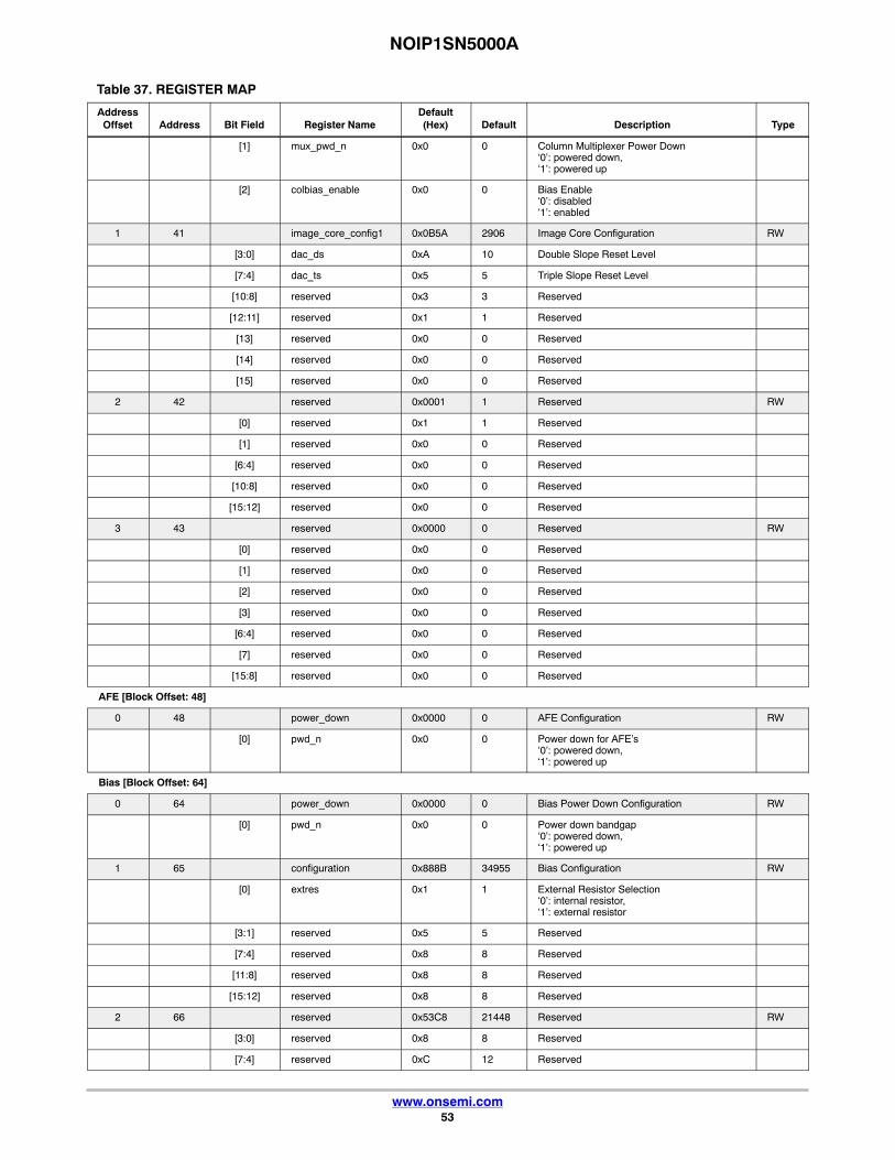
NOIP1SN5000A
www.onsemi.com53
Table 37. REGISTER MAP
AddressOffset TypeDescriptionDefault
Default(Hex)Register NameBit FieldAddress
[1] mux_pwd_n 0x0 0 Column Multiplexer Power Down‘0’: powered down,‘1’: powered up
[2] colbias_enable 0x0 0 Bias Enable‘0’: disabled‘1’: enabled
1 41 image_core_config1 0x0B5A 2906 Image Core Configuration RW
[3:0] dac_ds 0xA 10 Double Slope Reset Level
[7:4] dac_ts 0x5 5 Triple Slope Reset Level
[10:8] reserved 0x3 3 Reserved
[12:11] reserved 0x1 1 Reserved
[13] reserved 0x0 0 Reserved
[14] reserved 0x0 0 Reserved
[15] reserved 0x0 0 Reserved
2 42 reserved 0x0001 1 Reserved RW
[0] reserved 0x1 1 Reserved
[1] reserved 0x0 0 Reserved
[6:4] reserved 0x0 0 Reserved
[10:8] reserved 0x0 0 Reserved
[15:12] reserved 0x0 0 Reserved
3 43 reserved 0x0000 0 Reserved RW
[0] reserved 0x0 0 Reserved
[1] reserved 0x0 0 Reserved
[2] reserved 0x0 0 Reserved
[3] reserved 0x0 0 Reserved
[6:4] reserved 0x0 0 Reserved
[7] reserved 0x0 0 Reserved
[15:8] reserved 0x0 0 Reserved
AFE [Block Offset: 48]
0 48 power_down 0x0000 0 AFE Configuration RW
[0] pwd_n 0x0 0 Power down for AFE’s‘0’: powered down,‘1’: powered up
Bias [Block Offset: 64]
0 64 power_down 0x0000 0 Bias Power Down Configuration RW
[0] pwd_n 0x0 0 Power down bandgap‘0’: powered down,‘1’: powered up
1 65 configuration 0x888B 34955 Bias Configuration RW
[0] extres 0x1 1 External Resistor Selection‘0’: internal resistor,‘1’: external resistor
[3:1] reserved 0x5 5 Reserved
[7:4] reserved 0x8 8 Reserved
[11:8] reserved 0x8 8 Reserved
[15:12] reserved 0x8 8 Reserved
2 66 reserved 0x53C8 21448 Reserved RW
[3:0] reserved 0x8 8 Reserved
[7:4] reserved 0xC 12 Reserved

NOIP1SN5000A
www.onsemi.com54
Table 37. REGISTER MAP
AddressOffset TypeDescriptionDefault
Default(Hex)Register NameBit FieldAddress
[14:8] reserved 0x53 83 Reserved
3 67 reserved 0x8888 34952 Reserved RW
[3:0] reserved 0x8 8 Reserved
[7:4] reserved 0x8 8 Reserved
[11:8] reserved 0x8 8 Reserved
[15:12] reserved 0x8 8 Reserved
4 68 lvds_bias 0x0088 136 LVDS Bias Configuration RW
[3:0] lvds_ibias 0x8 8 LVDS Ibias
[7:4] lvds_iref 0x8 8 LVDS Iref
5 69 reserved 0x0888 2184 Reserved RW
[3:0] reserved 0x8 8 Reserved
[7:4] reserved 0x8 8 Reserved
[11:8] reserved 0x8 8 Reserved
6 70 reserved 0x8888 34952 Reserved RW
[3:0] reserved 0x8 8 Reserved
[7:4] reserved 0x8 8 Reserved
[11:8] reserved 0x8 8 Reserved
[15:12] reserved 0x8 8 Reserved
7 71 reserved 0x8888 34952 Reserved RW
[15:0] reserved 0x8888 34952 Reserved
Charge Pump [Block Offset: 72]
0 72 configuration 0x2220 8736 Charge Pump Configuration RW
[0] trans_pwd_n 0x0 0 PD Trans Charge Pump Enable‘0’: disabled,‘1’: enabled
[1] resfd_calib_pwd_n 0x0 0 FD Charge Pump Enable‘0’: disabled,‘1’: enabled
[2] sel_sample_pwd_n 0x0 0 Select/Sample Charge Pump Enable‘0’: disabled‘1’: enabled
[6:4] reserved 0x2 2 Reserved
[10:8] reserved 0x2 2 Reserved
[14:12] reserved 0x2 2 Reserved
Charge Pump [Block Offset: 80]
0 80 reserved 0x0000 0 Reserved RW
[1:0] reserved 0x0 0 Reserved
[3:2] reserved 0x0 0 Reserved
[5:4] reserved 0x0 0 Reserved
[7:6] reserved 0x0 0 Reserved
[9:8] reserved 0x0 0 Reserved
1 81 reserved 0x8881 34945 Reserved RW
[15:0] reserved 0x8881 34945 Reserved
Temperature Sensor [Block Offset: 96]
0 96 enable 0x0000 0 Temperature Sensor Configuration RW
[0] enable 0x0 0 Temperature Diode Enable‘0’: disabled,‘1’: enabled

NOIP1SN5000A
www.onsemi.com55
Table 37. REGISTER MAP
AddressOffset TypeDescriptionDefault
Default(Hex)Register NameBit FieldAddress
[1] reserved 0x0 0 Reserved
[2] reserved 0x0 0 Reserved
[3] reserved 0x0 0 Reserved
[4] reserved 0x0 0 Reserved
[5] reserved 0x0 0 Reserved
[13:8] offset 0x0 0 Temperature Offset (signed)
1 97 temp 0x0000 0 Temperature Sensor Status Status
[7:0] temp 0x00 0 Temperature Readout
Temperature Sensor [Block Offset: 104]
0 104 reserved 0x0000 0 Reserved RW
[15:0] reserved 0x0 0 Reserved
1 105 reserved 0x0000 0 Reserved RW
[1:0] reserved 0x0 0 Reserved
[6:2] reserved 0x0 0 Reserved
[7] reserved 0x0 0 Reserved
[9:8] reserved 0x0 0 Reserved
[14:10] reserved 0x0 0 Reserved
[15] reserved 0x0 0 Reserved
2 106 reserved 0x0000 0 Reserved Status
[15:0] reserved 0x0000 0 Reserved
3 107 reserved 0x0000 0 Reserved Status
[15:0] reserved 0x0000 0 Reserved
4 108 reserved 0x0000 0 Reserved Status
[15:0] reserved 0x0000 0 Reserved
5 109 reserved 0x0000 0 Reserved Status
[15:0] reserved 0x0000 0 Reserved
6 110 reserved 0x0000 0 Reserved Status
[15:0] reserved 0x0000 0 Reserved
7 111 reserved 0x0000 0 Reserved Status
[15:0] reserved 0x0000 0 Reserved
Serializers / LVDS / IO [Block Offset: 112]
0 112 power_down 0x0000 0 LVDS Power Down Configuration RW
[0] clock_out_pwd_n 0x0 0 Power down for Clock Output.‘0’: powered down,‘1’: powered up
[1] sync_pwd_n 0x0 0 Power down for Sync channel‘0’: powered down,‘1’: powered up
[2] data_pwd_n 0x0 0 Power down for data channels (4 channels)‘0’: powered down,‘1’: powered up
Sync Words [Block Offset: 116]
4 116 trainingpattern 0x03A6 934 Data Formating − Training Pattern RW
[9:0] trainingpattern 0x3A6 934 Training pattern sent on Data channels duringidle mode. This data is used to perform wordalignment on the LVDS data channels.
5 117 sync_code0 0x002A 42 LVDS Power Down Configuration RW
[6:0] frame_sync_0 0x02A 42 Frame Sync Code LSBs − Even kernels

NOIP1SN5000A
www.onsemi.com56
Table 37. REGISTER MAP
AddressOffset TypeDescriptionDefault
Default(Hex)Register NameBit FieldAddress
6 118 sync_code1 0x0015 21 Data Formating − BL Indication RW
[9:0] bl_0 0x015 21 Black Pixel Identification Sync Code − Evenkernels
7 119 sync_code2 0x0035 53 Data Formating − IMG Indication RW
[9:0] img_0 0x035 53 Valid Pixel Identification Sync Code − Evenkernels
8 120 sync_code3 0x0025 37 Data Formating − IMG Indication RW
[9:0] ref_0 0x025 37 Reference Pixel Identification Sync Code −Even kernels
9 121 sync_code4 0x002A 42 LVDS Power Down Configuration RW
[6:0] frame_sync_1 0x02A 42 Frame Sync Code LSBs − Odd kernels
10 122 sync_code5 0x0015 21 Data Formating − BL Indication RW
[9:0] bl_1 0x015 21 Black Pixel Identification Sync Code − Oddkernels
11 123 sync_code6 0x0035 53 Data Formating − IMG Indication RW
[9:0] img_1 0x035 53 Valid Pixel Identification Sync Code − Oddkernels
12 124 sync_code7 0x0025 37 Data Formating − IMG Indication RW
[9:0] ref_1 0x025 37 Reference Pixel Identification Sync Code −Odd kernels
13 125 sync_code8 0x0059 89 Data Formating − CRC Indication RW
[9:0] crc 0x059 89 CRC Value Identification Sync Code
14 126 sync_code9 0x03A6 934 Data Formating − TR Indication RW
[9:0] tr 0x3A6 934 Training Value Identification Sync Code
15 127 reserved 0x02AA 682 Reserved RW
[9:0] reserved 0x2AA 682 Reserved
Data Block [Block Offset: 128]
0 128 blackcal 0x4008 16392 Black Calibration Configuration RW
[7:0] black_offset 0x08 8 Desired black level at output
[10:8] black_samples 0x0 0 Black pixels taken into account for black cali-bration.Total samples = 2**black_samples
[14:11] reserved 0x8 8 Reserved
[15] crc_seed 0x0 0 CRC Seed‘0’: All−0‘1’: All−1
1 129 general_configuration 0x0001 1 Black Calibration and Data FormatingConfiguration
RW
[0] auto_blackcal_enable 0x1 1 Automatic blackcalibration is enabled when 1,bypassed when 0
[9:1] blackcal_offset 0x00 0 Black Calibration offset used when au-to_black_cal_en = ‘0’.
[10] blackcal_offset_dec 0x0 0 blackcal_offset is added when 0, subtractedwhen 1
[11] reserved 0x0 0 Reserved
[12] reserved 0x0 0 Reserved
[13] 8bit_mode 0x0 0 Shifts window ID indications by 4 cycles.‘0’: 10 bit mode,‘1’: 8 bit mode
[14] ref_mode 0x0 0 Data contained on reference lines:‘0’: reference pixels‘1’: black average for the corresponding datachannel

NOIP1SN5000A
www.onsemi.com57
Table 37. REGISTER MAP
AddressOffset TypeDescriptionDefault
Default(Hex)Register NameBit FieldAddress
[15] ref_bcal_enable 0x0 0 Enable black calibration on reference lines‘0’: Disabled‘1’: Enabled
2 130 reserved 0x000F 15 Reserved RW
[0] reserved 0x1 1 Reserved
[1] reserved 0x1 1 Reserved
[2] reserved 0x1 1 Reserved
[3] reserved 0x1 1 Reserved
[4] reserved 0x0 0 Reserved
[8] reserved 0x0 0 Reserved
8 136 blackcal_error0 0x0000 0 Black Calibration Status Status
[15:0] blackcal_error[15:0] 0x0000 0 Black Calibration Error. This flag is set whennot enough black samples are available.Black Calibration shall not be valid. Channels0−16
9 137 reserved 0x0000 0 Reserved Status
[15:0] reserved 0x0000 0 Reserved
10 138 reserved 0x0000 0 Reserved Status
[15:0] reserved 0x0000 0 Reserved
11 139 reserved 0x0000 0 Reserved Status
[15:0] reserved 0x0000 0 Reserved
12 140 reserved 0x0000 0 Reserved RW
[15:0] reserved 0x0000 0 Reserved
13 141 reserved 0xFFFF 65535 Reserved RW
[15:0] reserved 0xFFFF 65535 Reserved
16 144 test_configuration 0x0000 0 Data Formating Test Configuration RW
[0] testpattern_en 0x0 0 Insert synthesized testpattern when ‘1’
[1] inc_testpattern 0x0 0 Incrementing testpattern when ‘1’, constanttestpattern when ‘0’
[2] prbs_en 0x0 0 Insert PRBS when ‘1’
[3] frame_testpattern 0x0 0 Frame test patterns when ‘1’, unframed test-patterns when ‘0’
[4] reserved 0x0 0 Reserved
17 145 reserved 0x0000 0 Reserved RW
[15:0] reserved 0 Reserved
18 146 test_configuration0 0x0100 256 Data Formating Test Configuration RW
[7:0] testpattern0_lsb 0x00 0 Testpattern used on datapath #0 when testpattern_en = ‘1’.Note: Most significant bits are configured inregister 150.
[15:8] testpattern1_lsb 0x01 1 Testpattern used on datapath #1 when testpattern_en = ‘1’.Note: Most significant bits are configured inregister 150.
19 147 test_configuration1 0x0302 770 Data Formating Test Configuration RW
[7:0] testpattern2_lsb 0x02 2 Testpattern used on datapath #2 when testpattern_en = ‘1’.Note: Most significant bits are configured inregister 150.

NOIP1SN5000A
www.onsemi.com58
Table 37. REGISTER MAP
AddressOffset TypeDescriptionDefault
Default(Hex)Register NameBit FieldAddress
[15:8] testpattern3_lsb 0x03 3 Testpattern used on datapath #3 when testpattern_en = ‘1’.Note: Most significant bits are configured inregister 150.
20 148 test_configuration2 0x0504 1284 Data Formating Test Configuration RW
[7:0] testpattern4_lsb 0x04 4 Testpattern used on datapath #4 when testpattern_en = ‘1’.Note: Most significant bits are configured inregister 150.
[15:8] testpattern5_lsb 0x05 5 Testpattern used on datapath #5 when testpattern_en = ‘1’.Note: Most significant bits are configured inregister 150.
21 149 test_configuration3 0x0706 1798 Data Formating Test Configuration RW
[7:0] testpattern6_lsb 0x06 6 Testpattern used on datapath #6 when testpattern_en = ‘1’.Note: Most significant bits are configured inregister 150.
[15:8] testpattern7_lsb 0x07 7 Testpattern used on datapath #7 when testpattern_en = ‘1’.Note: Most significant bits are configured inregister 150.
22 150 test_configuration16 0x0000 0 Data Formating Test Configuration RW
[1:0] testpattern0_msb 0x0 0 Testpattern used when testpattern_en = ‘1’
[3:2] testpattern1_msb 0x0 0 Testpattern used when testpattern_en = ‘1’
[5:4] testpattern2_msb 0x0 0 Testpattern used when testpattern_en = ‘1’
[7:6] testpattern3_msb 0x0 0 Testpattern used when testpattern_en = ‘1’
[9:8] testpattern4_msb 0x0 0 Testpattern used when testpattern_en = ‘1’
[11:10] testpattern5_msb 0x0 0 Testpattern used when testpattern_en = ‘1’
[13:12] testpattern6_msb 0x0 0 Testpattern used when testpattern_en = ‘1’
[15:14] testpattern7_msb 0x0 0 Testpattern used when testpattern_en = ‘1’
26 154 reserved 0x0000 0 Reserved RW
[15:0] reserved 0x0000 0 Reserved
27 155 reserved 0x0000 0 Reserved RW
[15:0] reserved 0x0000 0 Reserved
AEC [Block Offset: 160]
0 160 configuration 0x0010 16 AEC Configuration RW
[0] enable 0x0 0 AEC Enable
[1] restart_filter 0x0 0 Restart AEC filter
[2] freeze 0x0 0 Freeze AEC filter and enforcer gains
[3] pixel_valid 0x0 0 Use every pixel from channel when 0, every4th pixel when 1
[4] amp_pri 0x1 1 Column amplifier gets higher priority than AFEPGA in gain distribution if 1. Vice versa if 0
1 161 intensity 0x60B8 24760 AEC Configuration RW
[9:0] desired_intensity 0xB8 184 Target average intensity
[15:10] reserved 0x018 24 Reserved
2 162 red_scale_factor 0x0080 128 Red Scale Factor RW
[9:0] red_scale_factor 0x80 128 Red Scale Factor3.7 unsigned

NOIP1SN5000A
www.onsemi.com59
Table 37. REGISTER MAP
AddressOffset TypeDescriptionDefault
Default(Hex)Register NameBit FieldAddress
3 163 green1_scale_factor 0x0080 128 Green1 Scale Factor RW
[9:0] green1_scale_factor 0x80 128 Green1 Scale Factor3.7 unsigned
4 164 green2_scale_factor 0x0080 128 Green2 Scale Factor RW
[9:0] green2_scale_factor 0x80 128 Green2 Scale Factor3.7 unsigned
5 165 blue_scale_factor 0x0080 128 Blue Scale Factor RW
[9:0] blue_scale_factor 0x80 128 Blue Scale Factor3.7 unsigned
6 166 reserved 0x03FF 1023 Reserved RW
[15:0] reserved 0x03FF 1023 Reserved
7 167 reserved 0x0800 2048 Reserved RW
[1:0] reserved 0x0 0 Reserved
[3:2] reserved 0x0 0 Reserved
[15:4] reserved 0x080 128 Reserved
8 168 min_exposure 0x0001 1 Minimum Exposure Time RW
[15:0] min_exposure 0x0001 1 Minimum Exposure Time
9 169 min_gain 0x0800 2048 Minimum Gain RW
[1:0] min_mux_gain 0x0 0 Minimum Column Amplifier Gain
[3:2] min_afe_gain 0x0 0 Minimum AFE PGA Gain
[15:4] min_digital_gain 0x080 128 Minimum Digital Gain5.7 unsigned
10 170 max_exposure 0x03FF 1023 Maximum Exposure Time RW
[15:0] max_exposure 0x03FF 1023 Maximum Exposure Time
11 171 max_gain 0x100D 4109 Maximum Gain RW
[1:0] max_mux_gain 0x1 1 Maximum Column Amplifier Gain
[3:2] max_afe_gain 0x3 3 Maximum AFE PGA Gain
[15:4] max_digital_gain 0x100 256 Maximum Digital Gain5.7 unsigned
12 172 reserved 0x0083 131 Reserved RW
[7:0] reserved 0x083 131 Reserved
[13:8] reserved 0x00 0 Reserved
[15:14] reserved 0x0 0 Reserved
13 173 reserved 0x2824 10276 Reserved RW
[7:0] reserved 0x024 36 Reserved
[15:8] reserved 0x028 40 Reserved
14 174 reserved 0x2A96 10902 Reserved RW
[3:0] reserved 0x6 6 Reserved
[7:4] reserved 0x9 9 Reserved
[11:8] reserved 0xA 10 Reserved
[15:12] reserved 0x2 2 Reserved
15 175 reserved 0x0080 128 Reserved RW
[9:0] reserved 0x080 128 Reserved
16 176 reserved 0x0100 256 Reserved RW
[9:0] reserved 0x100 256 Reserved
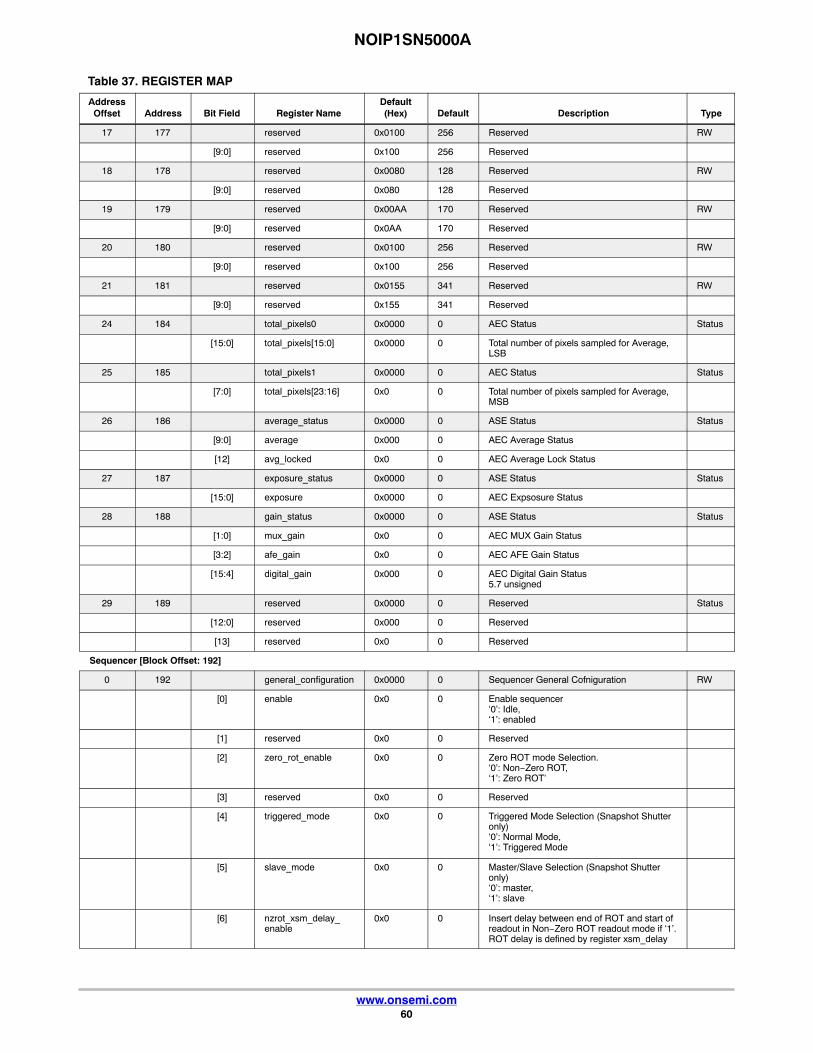
NOIP1SN5000A
www.onsemi.com60
Table 37. REGISTER MAP
AddressOffset TypeDescriptionDefault
Default(Hex)Register NameBit FieldAddress
17 177 reserved 0x0100 256 Reserved RW
[9:0] reserved 0x100 256 Reserved
18 178 reserved 0x0080 128 Reserved RW
[9:0] reserved 0x080 128 Reserved
19 179 reserved 0x00AA 170 Reserved RW
[9:0] reserved 0x0AA 170 Reserved
20 180 reserved 0x0100 256 Reserved RW
[9:0] reserved 0x100 256 Reserved
21 181 reserved 0x0155 341 Reserved RW
[9:0] reserved 0x155 341 Reserved
24 184 total_pixels0 0x0000 0 AEC Status Status
[15:0] total_pixels[15:0] 0x0000 0 Total number of pixels sampled for Average,LSB
25 185 total_pixels1 0x0000 0 AEC Status Status
[7:0] total_pixels[23:16] 0x0 0 Total number of pixels sampled for Average,MSB
26 186 average_status 0x0000 0 ASE Status Status
[9:0] average 0x000 0 AEC Average Status
[12] avg_locked 0x0 0 AEC Average Lock Status
27 187 exposure_status 0x0000 0 ASE Status Status
[15:0] exposure 0x0000 0 AEC Expsosure Status
28 188 gain_status 0x0000 0 ASE Status Status
[1:0] mux_gain 0x0 0 AEC MUX Gain Status
[3:2] afe_gain 0x0 0 AEC AFE Gain Status
[15:4] digital_gain 0x000 0 AEC Digital Gain Status5.7 unsigned
29 189 reserved 0x0000 0 Reserved Status
[12:0] reserved 0x000 0 Reserved
[13] reserved 0x0 0 Reserved
Sequencer [Block Offset: 192]
0 192 general_configuration 0x0000 0 Sequencer General Cofniguration RW
[0] enable 0x0 0 Enable sequencer‘0’: Idle,‘1’: enabled
[1] reserved 0x0 0 Reserved
[2] zero_rot_enable 0x0 0 Zero ROT mode Selection.‘0’: Non−Zero ROT,‘1’: Zero ROT’
[3] reserved 0x0 0 Reserved
[4] triggered_mode 0x0 0 Triggered Mode Selection (Snapshot Shutteronly)‘0’: Normal Mode,‘1’: Triggered Mode
[5] slave_mode 0x0 0 Master/Slave Selection (Snapshot Shutter only)‘0’: master,‘1’: slave
[6] nzrot_xsm_delay_enable
0x0 0 Insert delay between end of ROT and start ofreadout in Non−Zero ROT readout mode if ‘1’.ROT delay is defined by register xsm_delay

NOIP1SN5000A
www.onsemi.com61
Table 37. REGISTER MAP
AddressOffset TypeDescriptionDefault
Default(Hex)Register NameBit FieldAddress
[7] subsampling 0x0 0 Subsampling mode selection‘0’: no subsampling,‘1’: subsampling
[8] binning 0x0 0 Binning mode selection‘0’: no binning,‘1’: binning
[10] roi_aec_enable 0x0 0 Enable windowing for AEC Statistics.‘0’: Subsample all windows‘1’: Subsample configured window
[13:11] monitor_select 0x0 0 Control of the monitor pins
[14] reserved 0x0 0 Reserved
[15] sequence 0x0 0 Enable a sequenced readout with differentparameters for even and odd frames.
1 193 delay_configuration 0x0000 0 Sequencer delay configuration RW
[7:0] reserved 0x00 0 Reserved
[15:8] xsm_delay 0x00 0 Delay between ROT end and X−readout(Non−Zero ROT and Zero ROT mode)
Delay between ROT end and X−readout(Normal ROT mode with nzrot_xsm_delay_enable = ‘1’)
2 194 integration_control 0x00E4 228 Integration Control RW
[0] dual_slope_enable 0x0 0 Enable Dual Slope
[1] triple_slope_enable 0x0 0 Enable Triple Slope
[2] fr_mode 0x1 1 Representation of fr_length.‘0’: reset length‘1’: frame length
[3] reserved 0x0 0 Reserved
[4] int_priority 0x0 0 Integration Priority‘0’: Frame readout has priority over integration‘1’: Integration End has priority over framereadout
[5] halt_mode 0x1 1 The current frame will be completed when thesequencer is disabled and halt_mode = ‘1’.When ‘0’, the sensor stops immediately whendisabled, without finishing the current frame.
[6] fss_enable 0x1 1 Generation of Frame Sequence Start Synccode (FSS)‘0’: No generation of FSS‘1’: Generation of FSS
[7] fse_enable 0x1 1 Generation of Frame Sequence End Synccode (FSE)‘0’: No generation of FSE‘1’: Generation of FSE
[8] reverse_y 0x0 0 Reverse readout‘0’: bottom to top readout‘1’: top to bottom readout
[9] reserved 0x0 0 Reserved
[11:10] subsampling_mode 0x0 0 Subsampling mode0x0: Subsampling in x and y (VITA compatible)0x1: Subsampling in x, not y0x2: Subsampling in y, not x0x3: Subsampling in x an y
[13:12] binning_mode 0x0 0 Binning mode0x0: Binning in x and y (VITA compatible)0x1: Binning in x, not y0x2: Binning in y, not x0x3: Binning in x an y
[14] reserved 0x0 0 Reserved
[15] reserved 0x0 0 Reserved
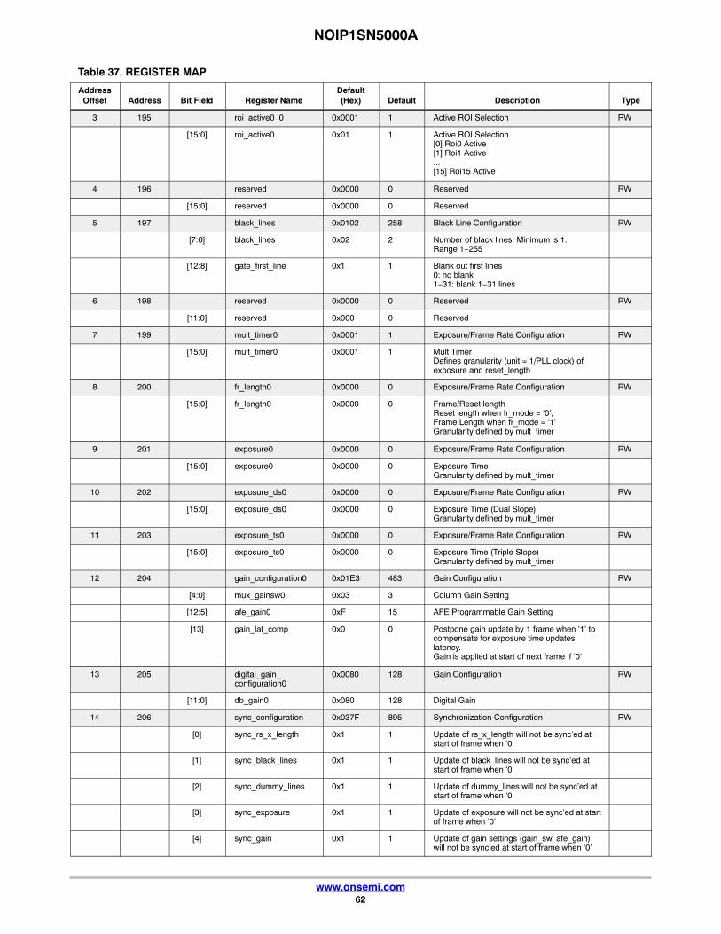
NOIP1SN5000A
www.onsemi.com62
Table 37. REGISTER MAP
AddressOffset TypeDescriptionDefault
Default(Hex)Register NameBit FieldAddress
3 195 roi_active0_0 0x0001 1 Active ROI Selection RW
[15:0] roi_active0 0x01 1 Active ROI Selection[0] Roi0 Active[1] Roi1 Active...[15] Roi15 Active
4 196 reserved 0x0000 0 Reserved RW
[15:0] reserved 0x0000 0 Reserved
5 197 black_lines 0x0102 258 Black Line Configuration RW
[7:0] black_lines 0x02 2 Number of black lines. Minimum is 1.Range 1−255
[12:8] gate_first_line 0x1 1 Blank out first lines0: no blank1−31: blank 1−31 lines
6 198 reserved 0x0000 0 Reserved RW
[11:0] reserved 0x000 0 Reserved
7 199 mult_timer0 0x0001 1 Exposure/Frame Rate Configuration RW
[15:0] mult_timer0 0x0001 1 Mult TimerDefines granularity (unit = 1/PLL clock) of exposure and reset_length
8 200 fr_length0 0x0000 0 Exposure/Frame Rate Configuration RW
[15:0] fr_length0 0x0000 0 Frame/Reset lengthReset length when fr_mode = ‘0’, Frame Length when fr_mode = ‘1’Granularity defined by mult_timer
9 201 exposure0 0x0000 0 Exposure/Frame Rate Configuration RW
[15:0] exposure0 0x0000 0 Exposure TimeGranularity defined by mult_timer
10 202 exposure_ds0 0x0000 0 Exposure/Frame Rate Configuration RW
[15:0] exposure_ds0 0x0000 0 Exposure Time (Dual Slope)Granularity defined by mult_timer
11 203 exposure_ts0 0x0000 0 Exposure/Frame Rate Configuration RW
[15:0] exposure_ts0 0x0000 0 Exposure Time (Triple Slope)Granularity defined by mult_timer
12 204 gain_configuration0 0x01E3 483 Gain Configuration RW
[4:0] mux_gainsw0 0x03 3 Column Gain Setting
[12:5] afe_gain0 0xF 15 AFE Programmable Gain Setting
[13] gain_lat_comp 0x0 0 Postpone gain update by 1 frame when ‘1’ tocompensate for exposure time updateslatency.Gain is applied at start of next frame if ‘0’
13 205 digital_gain_configuration0
0x0080 128 Gain Configuration RW
[11:0] db_gain0 0x080 128 Digital Gain
14 206 sync_configuration 0x037F 895 Synchronization Configuration RW
[0] sync_rs_x_length 0x1 1 Update of rs_x_length will not be sync’ed atstart of frame when ‘0’
[1] sync_black_lines 0x1 1 Update of black_lines will not be sync’ed atstart of frame when ‘0’
[2] sync_dummy_lines 0x1 1 Update of dummy_lines will not be sync’ed atstart of frame when ‘0’
[3] sync_exposure 0x1 1 Update of exposure will not be sync’ed at startof frame when ‘0’
[4] sync_gain 0x1 1 Update of gain settings (gain_sw, afe_gain)will not be sync’ed at start of frame when ‘0’
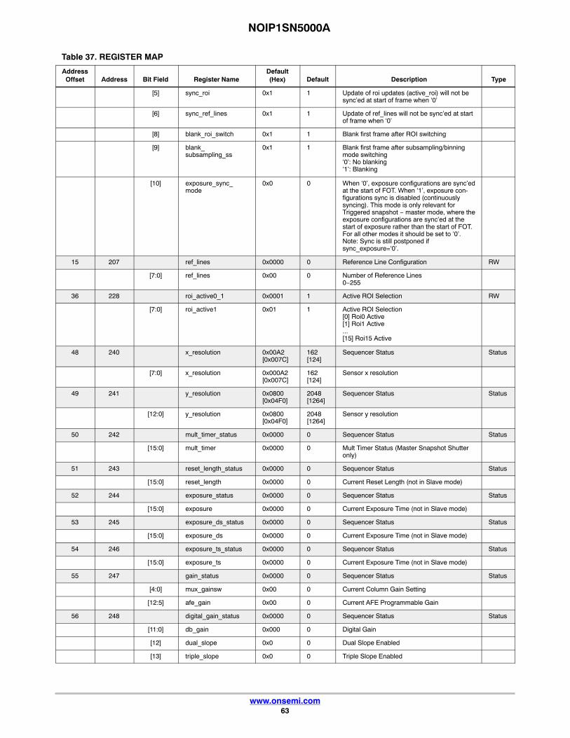
NOIP1SN5000A
www.onsemi.com63
Table 37. REGISTER MAP
AddressOffset TypeDescriptionDefault
Default(Hex)Register NameBit FieldAddress
[5] sync_roi 0x1 1 Update of roi updates (active_roi) will not besync’ed at start of frame when ‘0’
[6] sync_ref_lines 0x1 1 Update of ref_lines will not be sync’ed at startof frame when ‘0’
[8] blank_roi_switch 0x1 1 Blank first frame after ROI switching
[9] blank_subsampling_ss
0x1 1 Blank first frame after subsampling/binningmode switching‘0’: No blanking‘1’: Blanking
[10] exposure_sync_mode
0x0 0 When ‘0’, exposure configurations are sync’edat the start of FOT. When ‘1’, exposure con-figurations sync is disabled (continuouslysyncing). This mode is only relevant for Triggered snapshot − master mode, where theexposure configurations are sync’ed at thestart of exposure rather than the start of FOT.For all other modes it should be set to ‘0’.Note: Sync is still postponed if sync_exposure=‘0’.
15 207 ref_lines 0x0000 0 Reference Line Configuration RW
[7:0] ref_lines 0x00 0 Number of Reference Lines0−255
36 228 roi_active0_1 0x0001 1 Active ROI Selection RW
[7:0] roi_active1 0x01 1 Active ROI Selection[0] Roi0 Active[1] Roi1 Active...[15] Roi15 Active
48 240 x_resolution 0x00A2[0x007C]
162[124]
Sequencer Status Status
[7:0] x_resolution 0x000A2[0x007C]
162[124]
Sensor x resolution
49 241 y_resolution 0x0800[0x04F0]
2048[1264]
Sequencer Status Status
[12:0] y_resolution 0x0800[0x04F0]
2048[1264]
Sensor y resolution
50 242 mult_timer_status 0x0000 0 Sequencer Status Status
[15:0] mult_timer 0x0000 0 Mult Timer Status (Master Snapshot Shutteronly)
51 243 reset_length_status 0x0000 0 Sequencer Status Status
[15:0] reset_length 0x0000 0 Current Reset Length (not in Slave mode)
52 244 exposure_status 0x0000 0 Sequencer Status Status
[15:0] exposure 0x0000 0 Current Exposure Time (not in Slave mode)
53 245 exposure_ds_status 0x0000 0 Sequencer Status Status
[15:0] exposure_ds 0x0000 0 Current Exposure Time (not in Slave mode)
54 246 exposure_ts_status 0x0000 0 Sequencer Status Status
[15:0] exposure_ts 0x0000 0 Current Exposure Time (not in Slave mode)
55 247 gain_status 0x0000 0 Sequencer Status Status
[4:0] mux_gainsw 0x00 0 Current Column Gain Setting
[12:5] afe_gain 0x00 0 Current AFE Programmable Gain
56 248 digital_gain_status 0x0000 0 Sequencer Status Status
[11:0] db_gain 0x000 0 Digital Gain
[12] dual_slope 0x0 0 Dual Slope Enabled
[13] triple_slope 0x0 0 Triple Slope Enabled

NOIP1SN5000A
www.onsemi.com64
Table 37. REGISTER MAP
AddressOffset TypeDescriptionDefault
Default(Hex)Register NameBit FieldAddress
61 253 roi_aec_configuration0
0x0000 0 AEC ROI Configuration RW
[7:0] x_start 0x00 0 AEC ROI X Start Configuration (used for AECstatistics when roi_aec_enable=‘1’)
[15:8] x_end 0x00 0 AEC ROI X End Configuration (used for AECstatistics when roi_aec_enable=‘1’)
62 254 roi_aec_configuration1
0x0000 0 AEC ROI Configuration RW
[12:0] y_start 0x0000 0 AEC ROI Y Start Configuration (used for AECstatistics when roi_aec_enable=‘1’)
63 255 roi_aec_configuration2
0x0000 0 AEC ROI Configuration RW
[12:0] y_end 0x0000 0 AEC ROI Y End Configuration (used for AECstatistics when roi_aec_enable=‘1’)
Sequencer ROI [Block Offset: 256]
0 256 roi0_configuration0 0xA100 41216 ROI Configuration RW
[7:0] x_start 0x00 0 X Start Configuration
[15:8] x_end 0xA1 161 X End Configuration
1 257 roi0_configuration1 0x0000 0 ROI Configuration RW
[12:0] y_start 0x0000 0 Y Start Configuration
2 258 roi0_configuration2 0x07FF 2047 ROI Configuration RW
[12:0] y_end 0x7FF 2047 Y End Configuration
3 259 roi1_configuration0 0xA100 41216 ROI Configuration RW
[7:0] x_start 0x00 0 X Start Configuration
[15:8] x_end 0xA1 161 X End Configuration
4 260 roi1_configuration1 0x0000 0 ROI Configuration RW
[12:0] y_start 0x0000 0 Y Start Configuration
5 261 roi1_configuration2 0x07FF 2047 ROI Configuration RW
[12:0] y_end 0x7FF 2047 Y End Configuration
6 262 roi2_configuration0 0xA100 41216 ROI Configuration RW
[7:0] x_start 0x00 0 X Start Configuration
[15:8] x_end 0xA1 161 X End Configuration
7 263 roi2_configuration1 0x0000 0 ROI Configuration RW
[12:0] y_start 0x0000 0 Y Start Configuration
8 264 roi2_configuration2 0x07FF 2047 ROI Configuration RW
[12:0] y_end 0x7FF 2047 Y End Configuration
9 265 roi3_configuration0 0xA100 41216 ROI Configuration RW
[7:0] x_start 0x00 0 X Start Configuration
[15:8] x_end 0xA1 161 X End Configuration
10 266 roi3_configuration1 0x0000 0 ROI Configuration RW
[12:0] y_start 0x0000 0 Y Start Configuration
11 267 roi3_configuration2 0x07FF 2047 ROI Configuration RW
[12:0] y_end 0x7FF 2047 Y End Configuration
12 268 roi4_configuration0 0xA100 41216 ROI Configuration RW
[7:0] x_start 0x00 0 X Start Configuration
[15:8] x_end 0xA1 161 X End Configuration
13 269 roi4_configuration1 0x0000 0 ROI Configuration RW
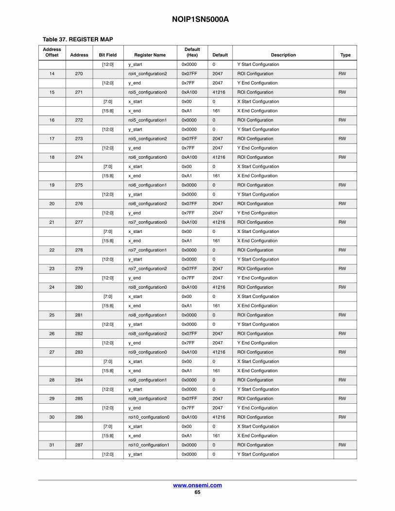
NOIP1SN5000A
www.onsemi.com65
Table 37. REGISTER MAP
AddressOffset TypeDescriptionDefault
Default(Hex)Register NameBit FieldAddress
[12:0] y_start 0x0000 0 Y Start Configuration
14 270 roi4_configuration2 0x07FF 2047 ROI Configuration RW
[12:0] y_end 0x7FF 2047 Y End Configuration
15 271 roi5_configuration0 0xA100 41216 ROI Configuration RW
[7:0] x_start 0x00 0 X Start Configuration
[15:8] x_end 0xA1 161 X End Configuration
16 272 roi5_configuration1 0x0000 0 ROI Configuration RW
[12:0] y_start 0x0000 0 Y Start Configuration
17 273 roi5_configuration2 0x07FF 2047 ROI Configuration RW
[12:0] y_end 0x7FF 2047 Y End Configuration
18 274 roi6_configuration0 0xA100 41216 ROI Configuration RW
[7:0] x_start 0x00 0 X Start Configuration
[15:8] x_end 0xA1 161 X End Configuration
19 275 roi6_configuration1 0x0000 0 ROI Configuration RW
[12:0] y_start 0x0000 0 Y Start Configuration
20 276 roi6_configuration2 0x07FF 2047 ROI Configuration RW
[12:0] y_end 0x7FF 2047 Y End Configuration
21 277 roi7_configuration0 0xA100 41216 ROI Configuration RW
[7:0] x_start 0x00 0 X Start Configuration
[15:8] x_end 0xA1 161 X End Configuration
22 278 roi7_configuration1 0x0000 0 ROI Configuration RW
[12:0] y_start 0x0000 0 Y Start Configuration
23 279 roi7_configuration2 0x07FF 2047 ROI Configuration RW
[12:0] y_end 0x7FF 2047 Y End Configuration
24 280 roi8_configuration0 0xA100 41216 ROI Configuration RW
[7:0] x_start 0x00 0 X Start Configuration
[15:8] x_end 0xA1 161 X End Configuration
25 281 roi8_configuration1 0x0000 0 ROI Configuration RW
[12:0] y_start 0x0000 0 Y Start Configuration
26 282 roi8_configuration2 0x07FF 2047 ROI Configuration RW
[12:0] y_end 0x7FF 2047 Y End Configuration
27 283 roi9_configuration0 0xA100 41216 ROI Configuration RW
[7:0] x_start 0x00 0 X Start Configuration
[15:8] x_end 0xA1 161 X End Configuration
28 284 roi9_configuration1 0x0000 0 ROI Configuration RW
[12:0] y_start 0x0000 0 Y Start Configuration
29 285 roi9_configuration2 0x07FF 2047 ROI Configuration RW
[12:0] y_end 0x7FF 2047 Y End Configuration
30 286 roi10_configuration0 0xA100 41216 ROI Configuration RW
[7:0] x_start 0x00 0 X Start Configuration
[15:8] x_end 0xA1 161 X End Configuration
31 287 roi10_configuration1 0x0000 0 ROI Configuration RW
[12:0] y_start 0x0000 0 Y Start Configuration

NOIP1SN5000A
www.onsemi.com66
Table 37. REGISTER MAP
AddressOffset TypeDescriptionDefault
Default(Hex)Register NameBit FieldAddress
32 288 roi10_configuration2 0x07FF 2047 ROI Configuration RW
[12:0] y_end 0x7FF 2047 Y End Configuration
33 289 roi11_configuration0 0xA100 41216 ROI Configuration RW
[7:0] x_start 0x00 0 X Start Configuration
[15:8] x_end 0xA1 161 X End Configuration
34 290 roi11_configuration1 0x0000 0 ROI Configuration RW
[12:0] y_start 0x0000 0 Y Start Configuration
35 291 roi11_configuration2 0x07FF 2047 ROI Configuration RW
[12:0] y_end 0x7FF 2047 Y End Configuration
36 292 roi12_configuration0 0xA100 41216 ROI Configuration RW
[7:0] x_start 0x00 0 X Start Configuration
[15:8] x_end 0xA1 161 X End Configuration
37 293 roi12_configuration1 0x0000 0 ROI Configuration RW
[12:0] y_start 0x0000 0 Y Start Configuration
38 294 roi12_configuration2 0x07FF 2047 ROI Configuration RW
[12:0] y_end 0x7FF 2047 Y End Configuration
39 295 roi13_configuration0 0xA100 41216 ROI Configuration RW
[7:0] x_start 0x00 0 X Start Configuration
[15:8] x_end 0xA1 161 X End Configuration
40 296 roi13_configuration1 0x0000 0 ROI Configuration RW
[12:0] y_start 0x0000 0 Y Start Configuration
41 297 roi13_configuration2 0x07FF 2047 ROI Configuration RW
[12:0] y_end 0x7FF 2047 Y End Configuration
42 298 roi14_configuration0 0xA100 41216 ROI Configuration RW
[7:0] x_start 0x00 0 X Start Configuration
[15:8] x_end 0xA1 161 X End Configuration
43 299 roi14_configuration1 0x0000 0 ROI Configuration RW
[12:0] y_start 0x0000 0 Y Start Configuration
44 300 roi14_configuration2 0x07FF 2047 ROI Configuration RW
[12:0] y_end 0x7FF 2047 Y End Configuration
45 301 roi15_configuration0 0xA100 41216 ROI Configuration RW
[7:0] x_start 0x00 0 X Start Configuration
[15:8] x_end 0xA1 161 X End Configuration
46 302 roi15_configuration1 0x0000 0 ROI Configuration RW
[12:0] y_start 0x0000 0 Y Start Configuration
47 303 roi15_configuration2 0x07FF 2047 ROI Configuration RW
[12:0] y_end 0x7FF 2047 Y End Configuration

NOIP1SN5000A
www.onsemi.com67
Selectable Pin−OutThe PYTHON sensor has a built−in possibility to route
some of the internal signals to different pads at the side of thechip.
The pin−out is controlled by glob_config in thechip_configuration register, located at address 2. The twopossible pin outs in the 84 pin package are listed in Table 38.By default, 0x3 setting is selected.
Table 38. OPTIONS FOR PIN−OUT IN THE 84 PIN LCCPACKAGE
Pin Name(84−pin LCC)
Pin Name(84−pin LCC)
Pin No.(84−pin LCC)
glob_config = 0x3 glob_config = 0x1
doutn1 clock_outn 8
doutp1 clock_outp 9
clock_outn doutn1 14
clock_outp doutp1 15
syncn doutn6 29
syncp doutp6 30
doutn6 syncn 35
doutp6 syncp 36

NOIP1SN5000A
www.onsemi.com68
Pin ListThe PYTHON 2000 and PYTHON 5000 image sensors
are available in LVDS output configuration
(P1&P3−SN/SE/FN). The LVDS I/Os comply to theTIA/EIA−644−A Standard and the CMOS I/Os have 3.3 Vsignal level. Table 39 shows the pin list.
Table 39. PIN LIST FOR P1,P3−SN/SE/FN
Package Pin No. Pin Name I/O Type Direction Description
1 vdd_33 Supply 3.3 V Supply
2 nc No connect
3 mosi CMOS Input SPI Master Out − Slave In
4 miso CMOS Output SPI Master In − Slave Out
5 sck CMOS Input SPI Input Clock
6 gnd_18 Supply 1.8 V Ground
7 vdd_18 Supply 1.8 V Supply
8 doutn1 LVDS Output LVDS Data Output Channel #1 (Negative), Not connected for P3
9 doutp1 LVDS Output LVDS Data Output Channel #1 (Positive), Not connected for P3
10 doutn0 LVDS Output LVDS Data Output Channel #0 (Negative)
11 doutp0 LVDS Output LVDS Data Output Channel #0 (Positive)
12 nc No connect
13 nc No connect
14 clock_outn LVDS Output LVDS Clock Output (Negative)
15 clock_outp LVDS Output LVDS Clock Output (Positive)
16 doutn2 LVDS Output LVDS Data Output Channel #2 (Negative)
17 doutp2 LVDS Output LVDS Data Output Channel #2 (Positive)
18 doutn3 LVDS Output LVDS Data Output Channel #3 (Negative), Not connected for P3
19 doutp3 LVDS Output LVDS Data Output Channel #3 (Positive), Not connected for P3
20 gnd_18 Supply Supply 1.8 V Ground
21 vdd_18 Supply Supply 1.8 V Supply
22 nc No connect
23 vdd_33 Supply Supply 3.3 V Supply
24 gnd_33 Supply Supply 3.3 V Ground
25 doutn4 LVDS Output LVDS Data Output Channel #4 (Negative)
26 doutp4 LVDS Output LVDS Data Output Channel #4 (Positive)
27 doutn5 LVDS Output LVDS Data Output Channel #5 (Negative), Not connected for P3
28 doutp5 LVDS Output LVDS Data Output Channel #5 (Positive), Not connected for P3
29 syncn LVDS Output LVDS Sync Channel Output (Negative)
30 syncp LVDS Output LVDS Sync Channel Output (Positive)
31 nc No connect
32 nc No connect
33 doutn7 LVDS Output LVDS Data Output Channel #7 (Negative), Not connected for P3
34 doutp7 LVDS Output LVDS Data Output Channel #7 (Positive), Not connected for P3
35 doutn6 LVDS Output LVDS Data Output Channel #6 (Negative)
36 doutp6 LVDS Output LVDS Data Output Channel #6 (Positive)
37 vdd_33 Supply Supply 3.3 V Supply
38 gnd_33 Supply Supply 3.3 V Ground
39 gnd_18 Supply Supply 1.8 V Ground
40 vdd_18 Supply Supply 1.8 V Supply
41 lvds_clock_inn LVDS Input LVDS Clock Input (Negative)
42 lvds_clock_inp LVDS Input LVDS Clock Input (Positive)
43 nc No connect

NOIP1SN5000A
www.onsemi.com69
Table 39. PIN LIST FOR P1,P3−SN/SE/FN
Package Pin No. DescriptionDirectionI/O TypePin Name
44 clk_pll CMOS Input Reference Clock Input for PLL
45 vdd_18 Supply 1.8 V Supply
46 gnd_18 Supply Supply 1.8 V Ground
47 ibias_master Analog Master Bias Reference
48 nc No connect
49 vdd_33 Supply 3.3 V Supply
50 gnd_33 Supply 3.3 V Ground
51 nc No connect
52 nc No connect
53 nc No connect
54 nc No connect
55 nc No connect
56 nc No connect
57 vdd_pix Supply Pixel Array Supply
58 gnd_colpc Supply Pixel Array Ground
59 nc No connect
60 vdd_pix Supply Pixel Array Supply
61 gnd_colpc Supply Pixel Array Ground
62 gnd_33 Supply 3.3 V Ground
63 vdd_33 Supply 3.3 V Supply
64 nc No connect
65 gnd_colpc Supply Pixel Array Ground
66 vdd_pix Supply Pixel Array Supply
67 gnd_colpc Supply Pixel Array Ground
68 vdd_pix Supply Pixel Array Supply
69 nc No connect
70 trigger0 CMOS Input Trigger Input #0
71 trigger1 CMOS Input Trigger Input #1
72 nc No connect
73 nc No connect
74 nc No connect
75 nc No connect
76 nc No connect
77 trigger2 CMOS Input Trigger Input #2
78 monitor0 CMOS Output Monitor Output #0
79 vdd_33 Supply Supply 3.3 V supply
80 gnd_33 Supply Supply 3.3 V Ground
81 monitor1 CMOS Output Monitor Output #1
82 reset_n CMOS Input Sensor Reset (Active Low)
83 ss_n CMOS Input SPI Slave Select.
84 gnd_33 Supply Supply 3.3 V Ground
NOIP1SN5000A
www.onsemi.com70
Table 40. MECHANICAL SPECIFICATION FOR P1,P3−SN/SE/FN
Parameter Description Min Typ Max Units
Die
(with Pin 1 to the left center)Die thickness 725 �m
Die Size 14.7 x 14.25 mm2
Die center, X offset to the center of package −50 0 50 �m
Die center, Y offset to the center of the package −50 0 50 �m
Die position, tilt to the Die Attach Plane −1 0 1 deg
Die rotation accuracy (referenced to die scribe and lead fingers on package on all four sides)
−1 0 1 deg
Optical center referenced from the die/package center (X−dir) −231 �m
Optical center referenced from the die/package center (Y−dir) 1697 �m
Distance from bottom of the package to top of the die surface 1.145 1.25 1.405 mm
Distance from top of the die surface to top of the glass lid 0.745 1.13 1.495 mm
Glass Lid Specification XY size 19 x 19 mm
Thickness 0.45 0.55 0.65 mm
Spectral response range 400 1000 nm
Transmission of glass lid (refer to Figure 52) 92 %
Glass Lid Material D263 Teco
Mechanical Shock JESD22−B104C; Condition G 2000 g
Vibration JESD22−B103B; Condition 1 2000 Hz
Mounting Profile Reflow profile according to J−STD−020D.1 260 °C
CTE Coefficient of Thermal expansion of the LCC Package 7.6 �m/°C

NOIP1SN5000A
www.onsemi.com71
Package Drawing
Figure 49. Package Drawing for the 84−pin LCC Package
NOTE: Unless noted otherwise, all dimensions represent nominal values.

NOIP1SN5000A
www.onsemi.com72
Optical Center InformationThe Center of the Die (CD) is the center of the cavity.The center of the die is exactly at 50% between the
outsides of the two outer seal ringsThe center of the cavity is exactly at 50% between the
insides of the finger pads.• Die outer dimensions:
♦ B4 is the reference for the Die (0,0) in �m♦ B1 is at (0, 14250) �m♦ B2 is at (14700, 14250) �m♦ B3 is at (14700, 0) �m
• Active Area outer dimensions♦ A1 is the at (881, 13754) �m♦ A2 is at (13356, 13754) �m♦ A3 is at (13356, 3890) �m♦ A4 is at (881, 3890) �m
• Center of the Active Area♦ AA is at (7119, 8822) �m
• Center of the Die♦ CD is at (7350, 7125) �m
Figure 50. Graphical Representation of the Optical Center
NOTE: Unless noted otherwise, all dimensions represent nominal values.
PYTHON5000 − Pixel (0,0)
Packing and Tray SpecificationThe PYTHON packing specification with
ON Semiconductor packing labels is packed as follows:
Table 41. PACKING AND TRAY INFORMATION FOR P1,P3−SN/SE/FN
LCC Package size typical (mm) Tray Restraint Box
Leads Length Width Thickness Tray Spec# Quantity / Tray Strap Bag Tray Quantity
84 19 19 2.33 KS−870541 42 Rubberband
Double bagged usingMBB and pink ESD
bag
5 trays + 1 covertray

NOIP1SN5000A
www.onsemi.com74
Glass LidThe PYTHON 2000 and PYTHON 5000 sensor uses a
glass lid without any coatings. Figure 52 shows thetransmission characteristics of the glass lid.
As shown in Figure 52, no infrared attenuating color filterglass is used. A filter must be provided in the optical path
when color devices are used (source:http://www.pgo−online.com).
Figure 52. Transmission Characteristics of the Glass Lid
Protective Film Option (−QTI Versions)For certain size and speed options, the sensor can be
delivered with a protective foil that is intended to beremoved after assembly. The dimensions of the foil are asillustrated in Figure 53 with the tab aligned towards onecorner of the package as illustrated in Fig 54.
Figure 53. Dimensions of the Tape
Figure 54. Location of Pull Tab in Relation to Pin 1of the Package

NOIP1SN5000A
www.onsemi.com75
SPECIFICATIONS AND USEFUL REFERENCES
The following references are available to customers underNDA at the ON Semiconductor Image Sensor Portal:https://www.onsemi.com/PowerSolutions/myon/erCispFolder.do• Product Acceptance Criteria
• Product Qualification Report
• PYTHON Developer’s Guide AND9362/D
Material Composition is available at:http://www.onsemi.com/PowerSolutions/MaterialComposition.do?searchParts=PYTHON5000
Useful ReferencesFor information on ESD and cover glass care and
cleanliness, please download the Image Sensor Handlingand Best Practices Application Note (AN52561/D) fromwww.onsemi.com.
For quality and reliability information, please downloadthe Quality & Reliability Handbook (HBD851/D) fromwww.onsemi.com.
For information on Standard terms and Conditions ofSale, please download Terms and Conditions fromwww.onsemi.com.
For information on acronyms and a glossary of termsused, please download Image Sensor Terminology(TND6116/D) from www.onsemi.com.
Return Material Authorization (RMA)Refer to the ON Semiconductor RMA policy procedure at
http://www.onsemi.com/site/pdf/CAT_Returns_FailureAnalysis.pdf
ON Semiconductor and the are registered trademarks of Semiconductor Components Industries, LLC (SCILLC) or its subsidiaries in the United States and/or other countries.SCILLC owns the rights to a number of patents, trademarks, copyrights, trade secrets, and other intellectual property. A listing of SCILLC’s product/patent coverage may be accessedat www.onsemi.com/site/pdf/Patent−Marking.pdf. SCILLC reserves the right to make changes without further notice to any products herein. SCILLC makes no warranty, representationor guarantee regarding the suitability of its products for any particular purpose, nor does SCILLC assume any liability arising out of the application or use of any product or circuit, andspecifically disclaims any and all liability, including without limitation special, consequential or incidental damages. “Typical” parameters which may be provided in SCILLC data sheetsand/or specifications can and do vary in different applications and actual performance may vary over time. All operating parameters, including “Typicals” must be validated for eachcustomer application by customer’s technical experts. SCILLC does not convey any license under its patent rights nor the rights of others. SCILLC products are not designed, intended,or authorized for use as components in systems intended for surgical implant into the body, or other applications intended to support or sustain life, or for any other application in whichthe failure of the SCILLC product could create a situation where personal injury or death may occur. Should Buyer purchase or use SCILLC products for any such unintended orunauthorized application, Buyer shall indemnify and hold SCILLC and its officers, employees, subsidiaries, affiliates, and distributors harmless against all claims, costs, damages, andexpenses, and reasonable attorney fees arising out of, directly or indirectly, any claim of personal injury or death associated with such unintended or unauthorized use, even if such claimalleges that SCILLC was negligent regarding the design or manufacture of the part. SCILLC is an Equal Opportunity/Affirmative Action Employer. This literature is subject to all applicablecopyright laws and is not for resale in any manner.
PUBLICATION ORDERING INFORMATIONN. American Technical Support: 800−282−9855 Toll FreeUSA/Canada
Europe, Middle East and Africa Technical Support:Phone: 421 33 790 2910
Japan Customer Focus CenterPhone: 81−3−5817−1050
NOIP1SN5000A/D
LITERATURE FULFILLMENT:Literature Distribution Center for ON Semiconductor19521 E. 32nd Pkwy, Aurora, Colorado 80011 USAPhone: 303−675−2175 or 800−344−3860 Toll Free USA/CanadaFax: 303−675−2176 or 800−344−3867 Toll Free USA/CanadaEmail: [email protected]
ON Semiconductor Website: www.onsemi.com
Order Literature: http://www.onsemi.com/orderlit
For additional information, please contact your localSales Representative