resetting asynchronous qdi systems
TRANSCRIPT
Resetting Asynchronous QDI Systems
Thesis by
Xiaofei Chang
In Partial Fulfillment of the Requirementsfor the Degree ofMaster of Science
California Institute of TechnologyPasadena, California
Submitted September, 2013

c© 2013Xiaofei Chang
All Rights Reserved

Acknowledgements
I wish to thank my advisor Dr. Alain Martin for his patience and guidance.Thanks also to my seniors Chris Moore and Sean Keller for their discussionand encouragement. At last, I would like to thank my wife for her supportand love.
i
Abstract
Quasi Delay-Insensitive (QDI) systems must be reset into a valid initial statebefore normal operation can start. Otherwise, deadlock may occur due towrong handshake communication between processes. This thesis first reviewsthe traditional Global Reset Schemes (GRS). It then proposes a new WaveReset Schemes (WRS). By utilizing the third possible value of QDI datacodes - reset value, WRS propagates the data with reset value and triggersLocal Reset (LR) sequentially. The global reset network for GRS can beremoved and all reset signals are generated locally for each process. Circuitstemplates as well as some special blocks are modified to accommodate thereset value in WRS. An algorithm is proposed to choose the proper LocalReset Input (LRI) in order to shorten reset time. WRS is then appliedto an iterative multiplier. The multiplier is proved working under differentoperating conditions.
ii
Contents
1 Introduction 1
2 GRS 32.1 Operation Protocol . . . . . . . . . . . . . . . . . . . . . . . . 32.2 Pipelines . . . . . . . . . . . . . . . . . . . . . . . . . . . . . . 5
2.2.1 Pipelines with Split Control and Datapath for GRS . . 52.2.1.1 Control Logic . . . . . . . . . . . . . . . . . . 62.2.1.2 Register . . . . . . . . . . . . . . . . . . . . . 82.2.1.3 Function Block . . . . . . . . . . . . . . . . . 92.2.1.4 Complete Pipeline Stage . . . . . . . . . . . . 10
2.2.2 Fine-Grain Integrated Pipelines for GRS . . . . . . . . 102.2.2.1 WCHB Dual-Rail Buffer for GRS . . . . . . . 102.2.2.2 PCHB Dual-Rail Buffer for GRS . . . . . . . 112.2.2.3 PCFB Dual-Rail Buffer for GRS . . . . . . . 13
3 WRS 153.1 Operation Protocol . . . . . . . . . . . . . . . . . . . . . . . . 153.2 Pipelines . . . . . . . . . . . . . . . . . . . . . . . . . . . . . . 16
3.2.1 Pipelines with Split Control and Datapath for WRS . . 163.2.1.1 Control Logic . . . . . . . . . . . . . . . . . . 173.2.1.2 Register . . . . . . . . . . . . . . . . . . . . . 183.2.1.3 Function Block . . . . . . . . . . . . . . . . . 193.2.1.4 Complete Pipeline Stage . . . . . . . . . . . . 20
3.2.2 Fine-Grain Integrated Pipelines for WRS . . . . . . . . 213.2.2.1 WCHB Dual-Rail Buffer for WRS . . . . . . 213.2.2.2 WCHB 1-of-4 Buffer for WRS . . . . . . . . . 233.2.2.3 PCHB Dual-Rail Buffers . . . . . . . . . . . . 253.2.2.4 PCFB Dual-Rail Buffers . . . . . . . . . . . . 253.2.2.5 Buffers with Logic . . . . . . . . . . . . . . . 26
3.3 Special Blocks . . . . . . . . . . . . . . . . . . . . . . . . . . . 313.3.1 Source/Sink . . . . . . . . . . . . . . . . . . . . . . . . 313.3.2 Initial Buffer . . . . . . . . . . . . . . . . . . . . . . . 323.3.3 Channel Arbiter . . . . . . . . . . . . . . . . . . . . . . 333.3.4 Slack Zero Process . . . . . . . . . . . . . . . . . . . . 35
4 Global Reset Insertion 384.1 Breadth First Search (BFS) . . . . . . . . . . . . . . . . . . . 394.2 Breadth First Search with Multiple Roots (BFSMR) . . . . . 39
iii
4.2.1 Pseudocode . . . . . . . . . . . . . . . . . . . . . . . . 404.2.2 Proof of Correctness . . . . . . . . . . . . . . . . . . . 40
4.2.2.1 Initialization . . . . . . . . . . . . . . . . . . 404.2.2.2 Maintenance . . . . . . . . . . . . . . . . . . 404.2.2.3 Termination . . . . . . . . . . . . . . . . . . . 41
5 Iterative Multiplier 435.1 Iterative Multiplier . . . . . . . . . . . . . . . . . . . . . . . . 435.2 Simulation . . . . . . . . . . . . . . . . . . . . . . . . . . . . . 44
6 Conclusion 48
Appendices 49
iv

List of Figures
1 Pipeline Stage with Split Control and Datapath for GRS . . . 62 Control Logic for GRS . . . . . . . . . . . . . . . . . . . . . . 73 Completion Tree . . . . . . . . . . . . . . . . . . . . . . . . . 84 Register for GRS . . . . . . . . . . . . . . . . . . . . . . . . . 85 Input Enable Generator for GRS . . . . . . . . . . . . . . . . 96 Function Block for GRS . . . . . . . . . . . . . . . . . . . . . 97 WCHB Dual-Rail Buffer for GRS . . . . . . . . . . . . . . . . 118 PCHB Dual-Rail Buffer for GRS . . . . . . . . . . . . . . . . 129 Reset Gate for C-element . . . . . . . . . . . . . . . . . . . . . 1210 PCFB Dual-Rail Buffer for GRS . . . . . . . . . . . . . . . . . 1311 Process with LRG for WRS . . . . . . . . . . . . . . . . . . . 1612 Pipeline Stage with Split Control and Datapath for WRS . . . 1713 Control Logic for WRS . . . . . . . . . . . . . . . . . . . . . . 1814 Register for WRS . . . . . . . . . . . . . . . . . . . . . . . . . 1915 Input Enable Generator for WRS . . . . . . . . . . . . . . . . 1916 Function Block for WRS . . . . . . . . . . . . . . . . . . . . . 2017 WCHB Dual-Rail Buffer for WRS 1 . . . . . . . . . . . . . . . 2218 WCHB Dual-Rail Buffer for WRS 2 . . . . . . . . . . . . . . . 2319 WCHB 1-of-4 Buffer for WRS . . . . . . . . . . . . . . . . . . 2420 PCHB Dual-Rail Buffer for WRS . . . . . . . . . . . . . . . . 2521 PCFB Dual-Rail Buffer for WRS . . . . . . . . . . . . . . . . 2622 Source for WRS . . . . . . . . . . . . . . . . . . . . . . . . . . 3123 Sink for WRS . . . . . . . . . . . . . . . . . . . . . . . . . . . 3124 Initial Buffer for WRS . . . . . . . . . . . . . . . . . . . . . . 3225 Channel Arbiter . . . . . . . . . . . . . . . . . . . . . . . . . . 3326 Basic Arbiter . . . . . . . . . . . . . . . . . . . . . . . . . . . 3427 Channel Arbiter for WRS . . . . . . . . . . . . . . . . . . . . 3528 Pseudocode of Breadth First Search (BFS) . . . . . . . . . . . 4029 Pseudocode of BFS with Multiple Roots . . . . . . . . . . . . 4130 Iterative Multiplier . . . . . . . . . . . . . . . . . . . . . . . . 4331 Reset Time for Different Process Corners . . . . . . . . . . . . 4532 Cycle Time for Different Process Corners . . . . . . . . . . . . 4633 Reset Time with Additional Global Reset . . . . . . . . . . . . 47
v
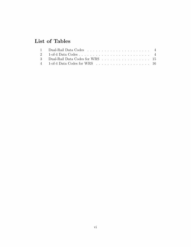
List of Tables
1 Dual-Rail Data Codes . . . . . . . . . . . . . . . . . . . . . . 42 1-of-4 Data Codes . . . . . . . . . . . . . . . . . . . . . . . . . 43 Dual-Rail Data Codes for WRS . . . . . . . . . . . . . . . . . 154 1-of-4 Data Codes for WRS . . . . . . . . . . . . . . . . . . . 16
vi
1 Introduction
Asynchronous systems with the only delay assumption of isochronic forksare called Quasi Delay-Insensitive (QDI) systems [1]. QDI systems are com-posed of concurrent modules called processes. Processes communicate witheach other by sending and receiving actions on channels. Each channel iscomprised of one or several directed data wires and one directed enable wire.Data wires from a sender process to a receiver process encode the messagebeing sent while the enable wire from a receiver process to a sender processis used to notify the sender process that the message has been received.
During normal operation, communication between processes occurs con-currently with computation inside each process. However, in order for a QDIsystem to transit into normal operation after power-on, it needs to be driveninto the valid initial state that is determined by Martin’s synthesis. Theprocedure that brings a system into its valid initial state after power-on iscalled reset. The valid initial state of a QDI system is determined by thevalid initial state of each process in the system. The valid initial state of aprocess is determined by valid initial values of all wires inside the process.Therefore each wire in the system needs to be driven to the valid initial valuebefore normal operation of the system starts.
This thesis discusses two methods to reset a QDI system, namely GlobalReset Scheme (GRS) and Wave Reset Scheme (WRS). They are different interms how they distribute the reset signal to each process. GRS distributesGlobal Reset (GR) to each process and resets them at the same time byasserting GR. For WRS, GR is connected to only a small number of pro-cesses. When GR is asserted, reset data is generated at the outputs of theseprocesses and propagates to other processes. Once reset data arrives at aprocess, it triggers Local Reset Generator (LRG) of that process. LRG as-serts Local Reset (LR) and forces the process to output reset data. The inputor inputs that drive LRG are Local Reset Input (LRI). This generation andpropagation of reset data continues until all processes have output reset data.
During reset phase, if no timing assumption other than isochronic fork [2]is made, the value of each wire needs to be checked to make sure the systemis in the valid initial state. However, checking each wire requires a largenumber of logic gates which introduce an unacceptable overhead in terms ofarea, delay and power consumption. Instead, a reset timing assumption ismade that guarantees the system will reach the valid initial state within resettime. Reset time is determined by the longest path that contains reset gatesat the head and tail and logic gates in between. GR needs to be asserted atleast as long as reset time in order for all wires to be driven to valid initial
1
values.The rest of the thesis is organized as follows. Section 2 and Section 3
respectively discuss GRS and WRS including operation protocol, pipelinetemplates and special blocks. Section 4 discusses the choice of LRI in orderto reduce reset time for WRS. The WRS is applied to a multiplier in Section5. Section 6 concludes the thesis.
2
2 GRS
For a given process P , the initial value of any input wire I is determinedby the gate inside the neighboring process that drives I. Initial values ofinternal wires and output wires are determined by gates inside P that drivethem. If initial values of input wires and corresponding gates can drive allinternal wires and output wires to the valid initial values, P will be resetto the valid initial state once neighboring processes have been reset to thevalid initial states. Otherwise, reset logic needs to be added in order to forceinternal wires and output wires to assume valid initial values.
Added reset logic converts logic gates into reset gates. Each reset gatehas an extra input that is connected to GR. When GR is asserted, the outputof a reset gate is driven to the valid initial value independent of the otherinputs. If all logic gates in a QDI system are converted into reset gates, thesystem is guaranteed to be in the valid initial state because GR forces eachwire to assume the valid initial value. However, converting all logic gates intoreset gates slow down normal operation of the system because reset gates areslower than corresponding logic gates. Therefore, only necessary logic gatesshould be converted into reset gates. To be more specific, only logic gatesthat can’t drive their outputs to valid initial values based on valid initialvalues of inputs should be converted into reset gates. Once there are enoughreset gates, each wire will be driven to the valid initial value when GR isasserted and the system will be driven to the valid initial state. After resetphase, GR is deasserted and normal operation starts. Reset gates functionin the same way as the original logic gates during normal operation.
2.1 Operation Protocol
Delay-Insensitive (DI) codes are used in QDI systems for data communica-tion. DI codes encode validity and neutrality of data within the data itself.There are many DI codes, among which dual-rail codes and 1-of-n codes arenormally used. Each wire in dual-rail codes or 1-of-n codes is used for onevalue of the data. When all wires are 0s, the data is neutral. When one of thewires is 1, the data is valid. For example, dual-rail codes are shown in Table 1.When (wire1, wire0) = (0, 0), data is neutral. When (wire0, wire1) = (0, 1)or (wire0, wire1) = (1, 0), data is valid 1 or valid 0. The rest combinationof values ((wire1, wire0) = (1, 1)) is invalid.
Similarly, 1-of-4 codes are shown in Table 2. When all four wires are 0s,the data is neutral. When one of the wires is 1, the data is respectively valid0, 1, 2, 3. All the other combinations of values are invalid.
3
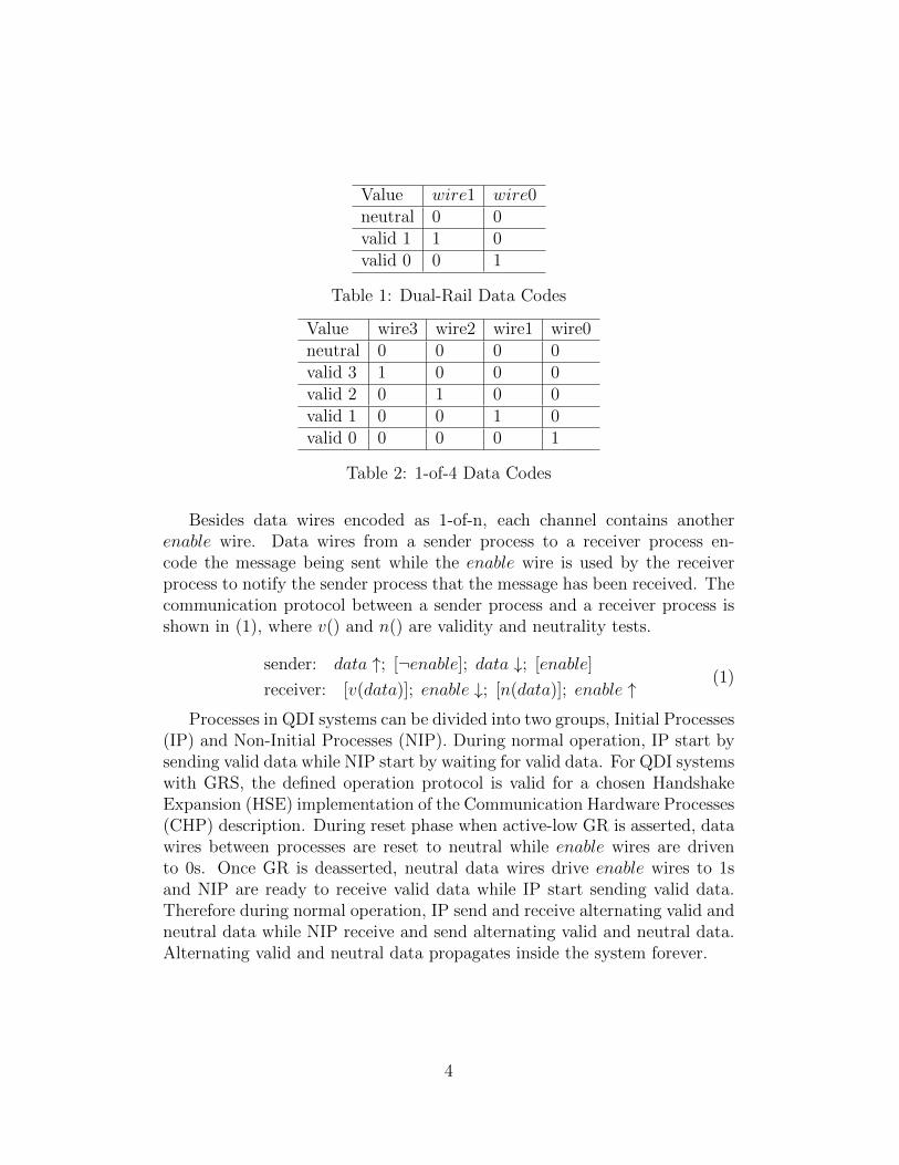
Value wire1 wire0neutral 0 0valid 1 1 0valid 0 0 1
Table 1: Dual-Rail Data Codes
Value wire3 wire2 wire1 wire0neutral 0 0 0 0valid 3 1 0 0 0valid 2 0 1 0 0valid 1 0 0 1 0valid 0 0 0 0 1
Table 2: 1-of-4 Data Codes
Besides data wires encoded as 1-of-n, each channel contains anotherenable wire. Data wires from a sender process to a receiver process en-code the message being sent while the enable wire is used by the receiverprocess to notify the sender process that the message has been received. Thecommunication protocol between a sender process and a receiver process isshown in (1), where v() and n() are validity and neutrality tests.
sender: data ↑; [¬enable]; data ↓; [enable]
receiver: [v(data)]; enable ↓; [n(data)]; enable ↑(1)
Processes in QDI systems can be divided into two groups, Initial Processes(IP) and Non-Initial Processes (NIP). During normal operation, IP start bysending valid data while NIP start by waiting for valid data. For QDI systemswith GRS, the defined operation protocol is valid for a chosen HandshakeExpansion (HSE) implementation of the Communication Hardware Processes(CHP) description. During reset phase when active-low GR is asserted, datawires between processes are reset to neutral while enable wires are drivento 0s. Once GR is deasserted, neutral data wires drive enable wires to 1sand NIP are ready to receive valid data while IP start sending valid data.Therefore during normal operation, IP send and receive alternating valid andneutral data while NIP receive and send alternating valid and neutral data.Alternating valid and neutral data propagates inside the system forever.
4
2.2 Pipelines
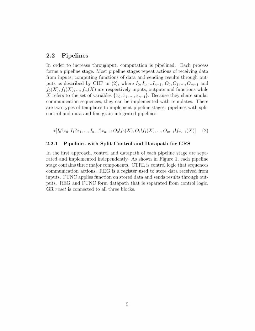
In order to increase throughput, computation is pipelined. Each processforms a pipeline stage. Most pipeline stages repeat actions of receiving datafrom inputs, computing functions of data and sending results through out-puts as described by CHP in (2), where I0, I1, ...In−1, O0, O1, ..., Om−1 andf0(X), f1(X), ..., fm(X) are respectively inputs, outputs and functions whileX refers to the set of variables {x0, x1, ..., xn−1}. Because they share similarcommunication sequences, they can be implemented with templates. Thereare two types of templates to implement pipeline stages: pipelines with splitcontrol and data and fine-grain integrated pipelines.
∗[I0?x0, I1?x1, ..., In−1?xn−1;O0!f0(X), O1!f1(X), ..., Om−1!fm−1(X)] (2)
2.2.1 Pipelines with Split Control and Datapath for GRS
In the first approach, control and datapath of each pipeline stage are sepa-rated and implemented independently. As shown in Figure 1, each pipelinestage contains three major components. CTRL is control logic that sequencescommunication actions. REG is a register used to store data received frominputs. FUNC applies function on stored data and sends results through out-puts. REG and FUNC form datapath that is separated from control logic.GR reset is connected to all three blocks.
5
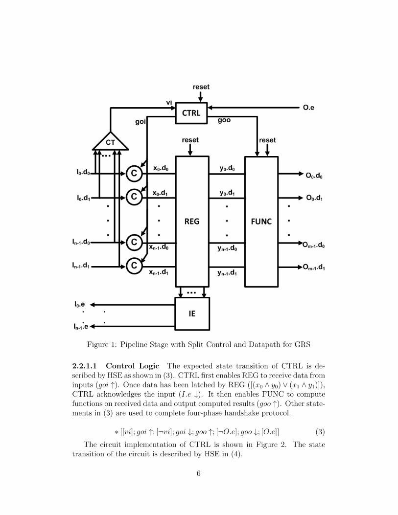
Figure 1: Pipeline Stage with Split Control and Datapath for GRS
2.2.1.1 Control Logic The expected state transition of CTRL is de-scribed by HSE as shown in (3). CTRL first enables REG to receive data frominputs (goi ↑). Once data has been latched by REG ([(x0 ∧ y0) ∨ (x1 ∧ y1)]),CTRL acknowledges the input (I.e ↓). It then enables FUNC to computefunctions on received data and output computed results (goo ↑). Other state-ments in (3) are used to complete four-phase handshake protocol.
∗ [[vi]; goi ↑; [¬vi]; goi ↓; goo ↑; [¬O.e]; goo ↓; [O.e]] (3)
The circuit implementation of CTRL is shown in Figure 2. The statetransition of the circuit is described by HSE in (4).
6
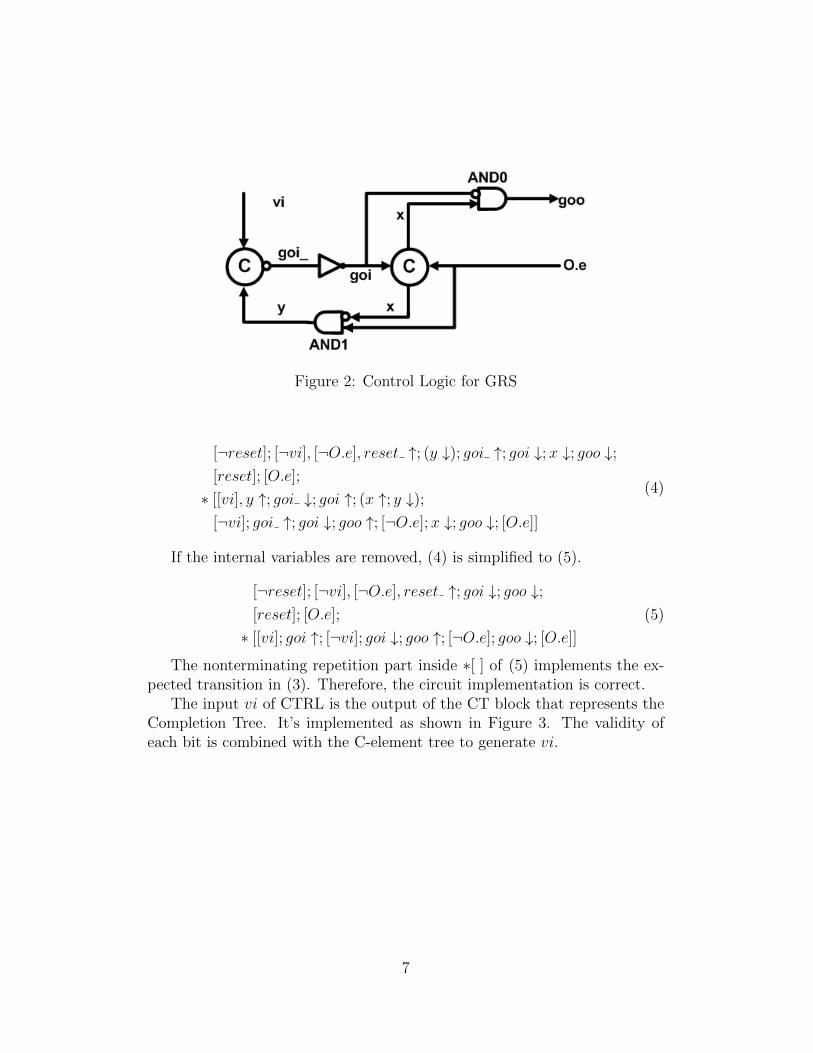
Figure 2: Control Logic for GRS
[¬reset]; [¬vi], [¬O.e], reset ↑; (y ↓); goi ↑; goi ↓;x ↓; goo ↓;[reset]; [O.e];
∗ [[vi], y ↑; goi ↓; goi ↑; (x ↑; y ↓);[¬vi]; goi ↑; goi ↓; goo ↑; [¬O.e];x ↓; goo ↓; [O.e]]
(4)
If the internal variables are removed, (4) is simplified to (5).
[¬reset]; [¬vi], [¬O.e], reset ↑; goi ↓; goo ↓;[reset]; [O.e];
∗ [[vi]; goi ↑; [¬vi]; goi ↓; goo ↑; [¬O.e]; goo ↓; [O.e]]
(5)
The nonterminating repetition part inside ∗[ ] of (5) implements the ex-pected transition in (3). Therefore, the circuit implementation is correct.
The input vi of CTRL is the output of the CT block that represents theCompletion Tree. It’s implemented as shown in Figure 3. The validity ofeach bit is combined with the C-element tree to generate vi.
7
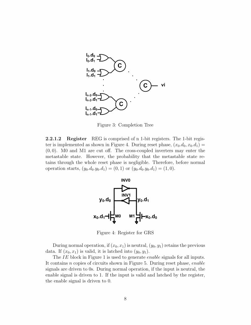
Figure 3: Completion Tree
2.2.1.2 Register REG is comprised of n 1-bit registers. The 1-bit regis-ter is implemented as shown in Figure 4. During reset phase, (x0.d0, x0.d1) =(0, 0). M0 and M1 are cut off. The cross-coupled inverters may enter themetastable state. However, the probability that the metastable state re-tains through the whole reset phase is negligible. Therefore, before normaloperation starts, (y0.d0.y0.d1) = (0, 1) or (y0.d0.y0.d1) = (1, 0).
Figure 4: Register for GRS
During normal operation, if (x0, x1) is neutral, (y0, y1) retains the previousdata. If (x0, x1) is valid, it is latched into (y0, y1).
The IE block in Figure 1 is used to generate enable signals for all inputs.It contains n copies of circuits shown in Figure 5. During reset phase, enablesignals are driven to 0s. During normal operation, if the input is neutral, theenable signal is driven to 1. If the input is valid and latched by the register,the enable signal is driven to 0.
8
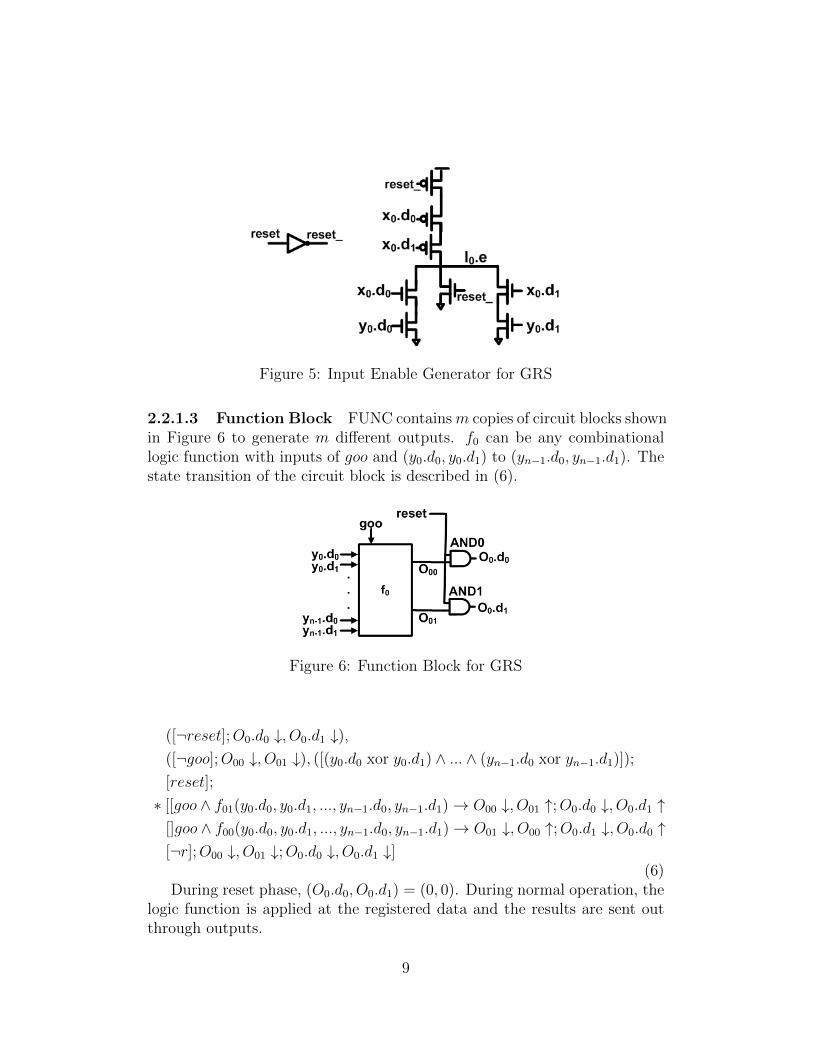
Figure 5: Input Enable Generator for GRS
2.2.1.3 Function Block FUNC contains m copies of circuit blocks shownin Figure 6 to generate m different outputs. f0 can be any combinationallogic function with inputs of goo and (y0.d0, y0.d1) to (yn−1.d0, yn−1.d1). Thestate transition of the circuit block is described in (6).
Figure 6: Function Block for GRS
([¬reset];O0.d0 ↓, O0.d1 ↓),([¬goo];O00 ↓, O01 ↓), ([(y0.d0 xor y0.d1) ∧ ... ∧ (yn−1.d0 xor yn−1.d1)]);
[reset];
∗ [[goo ∧ f01(y0.d0, y0.d1, ..., yn−1.d0, yn−1.d1)→ O00 ↓, O01 ↑;O0.d0 ↓, O0.d1 ↑[]goo ∧ f00(y0.d0, y0.d1, ..., yn−1.d0, yn−1.d1)→ O01 ↓, O00 ↑;O0.d1 ↓, O0.d0 ↑[¬r];O00 ↓, O01 ↓;O0.d0 ↓, O0.d1 ↓]
(6)During reset phase, (O0.d0, O0.d1) = (0, 0). During normal operation, the
logic function is applied at the registered data and the results are sent outthrough outputs.
9
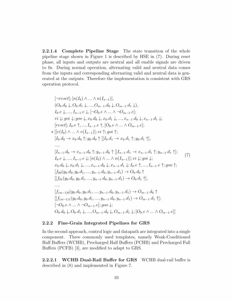
2.2.1.4 Complete Pipeline Stage The state transition of the wholepipeline stage shown in Figure 1 is described by HSE in (7). During resetphase, all inputs and outputs are neutral and all enable signals are drivento 0s. During normal operation, alternating valid and neutral data comesfrom the inputs and corresponding alternating valid and neutral data is gen-erated at the outputs. Therefore the implementation is consistent with GRSoperation protocol.
[¬reset]; [n(I0) ∧ ... ∧ n(In−1)],
(O0.d0 ↓, O0.d1 ↓, ..., Om−1.d0 ↓, Om−1.d1 ↓),I0.e ↓, ..., In−1.e ↓, [¬O0.e ∧ ... ∧ ¬Om−1.e];
vi ↓; goi ↓; goo ↓, x0.d0 ↓, x0.d1 ↓, ..., xn−1.d0 ↓, xn−1.d1 ↓;[reset]; I0.e ↑, ..., In−1.e ↑, [O0.e ∧ ... ∧Om−1.e];
∗ [[v(I0) ∧ ... ∧ v(In−1)]; vi ↑; goi ↑;[I0.d0 → x0.d0 ↑; y0.d0 ↑ []I0.d1 → x0.d1 ↑; y0.d1 ↑],...,
[In−1.d0 → xn−1.d0 ↑; yn−1.d0 ↑ []In−1.d1 → xn−1.d1 ↑; yn−1.d1 ↑];I0.e ↓, ..., In−1.e ↓; [n(I0) ∧ ... ∧ n(In−1)]; vi ↓; goi ↓;x0.d0 ↓, x0.d1 ↓, ..., xn−1.d0 ↓, xn−1.d1 ↓; I0.e ↑, ..., In−1.e ↑; goo ↑;[f00(y0.d0, y0.d1, ..., yn−1.d0, yn−1.d1)→ O0.d0 ↑[]f01(y0.d0, y0.d1, ..., yn−1.d0, yn−1.d1)→ O0.d1 ↑],...,
[f(m−1)0(y0.d0, y0.d1, ..., yn−1.d0, yn−1.d1)→ Om−1.d0 ↑[]f(m−1)1(y0.d0, y0.d1, ..., yn−1.d0, yn−1.d1)→ Om−1.d1 ↑];[¬O0.e ∧ ... ∧ ¬Om−1.e]; goo ↓;O0.d0 ↓, O0.d1 ↓, ..., Om−1.d0 ↓, Om−1.d1 ↓; [O0.e ∧ ... ∧Om−1.e]]
(7)
2.2.2 Fine-Grain Integrated Pipelines for GRS
In the second approach, control logic and datapath are integrated into a singlecomponent. Three commonly used templates, namely Weak-ConditionedHalf Buffers (WCHB), Precharged Half Buffers (PCHB) and Precharged FullBuffers (PCFB) [3], are modified to adapt to GRS.
2.2.2.1 WCHB Dual-Rail Buffer for GRS WCHB dual-rail buffer isdescribed in (8) and implemented in Figure 7.
10
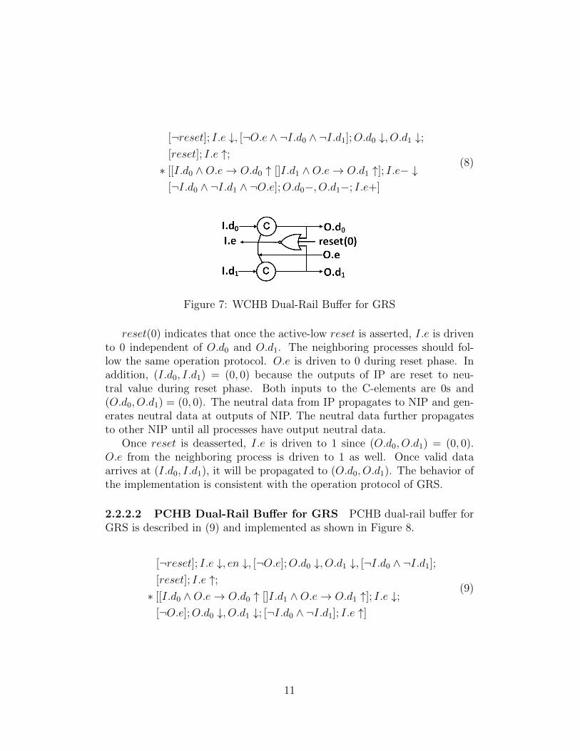
[¬reset]; I.e ↓, [¬O.e ∧ ¬I.d0 ∧ ¬I.d1];O.d0 ↓, O.d1 ↓;[reset]; I.e ↑;∗ [[I.d0 ∧O.e→ O.d0 ↑ []I.d1 ∧O.e→ O.d1 ↑]; I.e− ↓
[¬I.d0 ∧ ¬I.d1 ∧ ¬O.e];O.d0−, O.d1−; I.e+]
(8)
Figure 7: WCHB Dual-Rail Buffer for GRS
reset(0) indicates that once the active-low reset is asserted, I.e is drivento 0 independent of O.d0 and O.d1. The neighboring processes should fol-low the same operation protocol. O.e is driven to 0 during reset phase. Inaddition, (I.d0, I.d1) = (0, 0) because the outputs of IP are reset to neu-tral value during reset phase. Both inputs to the C-elements are 0s and(O.d0, O.d1) = (0, 0). The neutral data from IP propagates to NIP and gen-erates neutral data at outputs of NIP. The neutral data further propagatesto other NIP until all processes have output neutral data.
Once reset is deasserted, I.e is driven to 1 since (O.d0, O.d1) = (0, 0).O.e from the neighboring process is driven to 1 as well. Once valid dataarrives at (I.d0, I.d1), it will be propagated to (O.d0, O.d1). The behavior ofthe implementation is consistent with the operation protocol of GRS.
2.2.2.2 PCHB Dual-Rail Buffer for GRS PCHB dual-rail buffer forGRS is described in (9) and implemented as shown in Figure 8.
[¬reset]; I.e ↓, en ↓, [¬O.e];O.d0 ↓, O.d1 ↓, [¬I.d0 ∧ ¬I.d1];[reset]; I.e ↑;∗ [[I.d0 ∧O.e→ O.d0 ↑ []I.d1 ∧O.e→ O.d1 ↑]; I.e ↓;
[¬O.e];O.d0 ↓, O.d1 ↓; [¬I.d0 ∧ ¬I.d1]; I.e ↑]
(9)
11
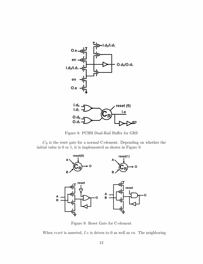
Figure 8: PCHB Dual-Rail Buffer for GRS
CR is the reset gate for a normal C-element. Depending on whether theinitial value is 0 or 1, it is implemented as shown in Figure 9.
Figure 9: Reset Gate for C-element
When reset is asserted, I.e is driven to 0 as well as en. The neighboring
12
processes should follow the same operation protocol. O.e is driven to 0 duringreset phase. Therefore O.d0 and O.d1 are driven to 0s. Similarly, the outputof the previous stage should be driven to (0, 0), i.e., (I.d0, I.d1) = (0, 0).
Once reset is deasserted, I.e is driven to 1 as well as en since (I.d0, I.d1) =(0, 0) and (O.d0, O.d1) = (0, 0). Similarly, O.e from the neighboring processis driven to 1. Once valid data arrives at (I.d0, I.d1), it will be propagatedto (O.d0, O.d1). The behavior of the implementation is consistent with theoperation protocol of GRS.
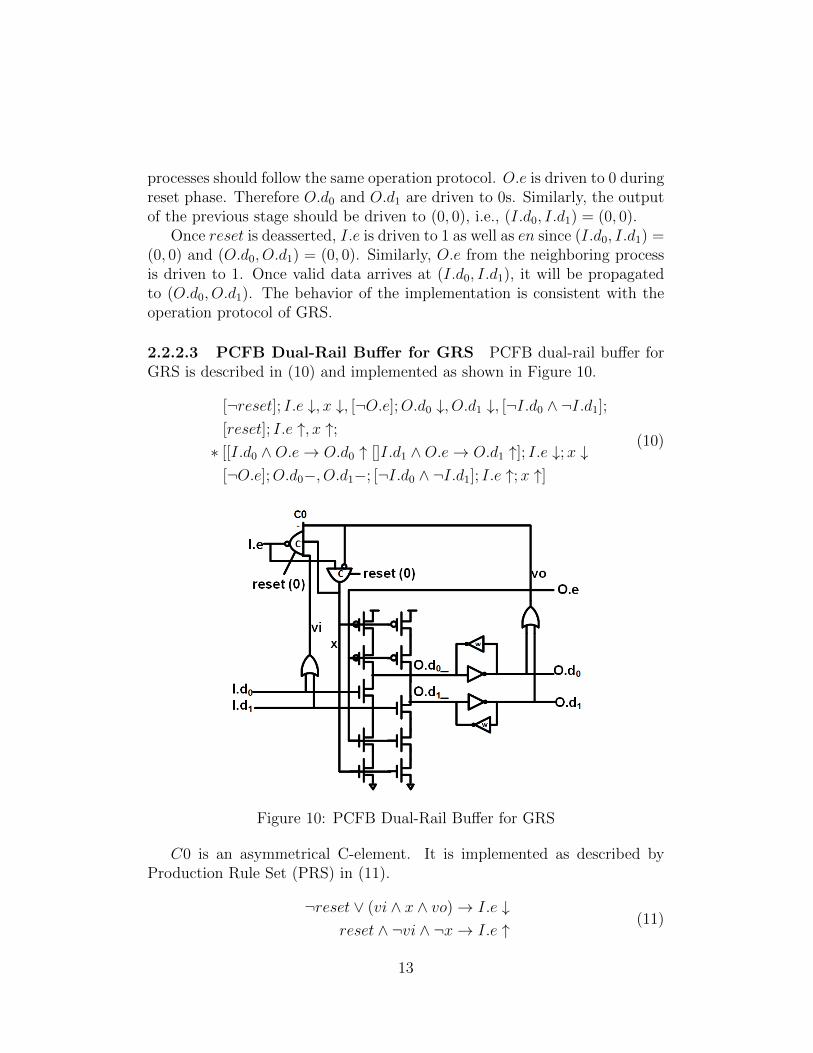
2.2.2.3 PCFB Dual-Rail Buffer for GRS PCFB dual-rail buffer forGRS is described in (10) and implemented as shown in Figure 10.
[¬reset]; I.e ↓, x ↓, [¬O.e];O.d0 ↓, O.d1 ↓, [¬I.d0 ∧ ¬I.d1];[reset]; I.e ↑, x ↑;∗ [[I.d0 ∧O.e→ O.d0 ↑ []I.d1 ∧O.e→ O.d1 ↑]; I.e ↓;x ↓
[¬O.e];O.d0−, O.d1−; [¬I.d0 ∧ ¬I.d1]; I.e ↑;x ↑]
(10)
Figure 10: PCFB Dual-Rail Buffer for GRS
C0 is an asymmetrical C-element. It is implemented as described byProduction Rule Set (PRS) in (11).
¬reset ∨ (vi ∧ x ∧ vo)→ I.e ↓reset ∧ ¬vi ∧ ¬x→ I.e ↑
(11)
13
When reset is asserted, I.e is driven to 0 as well as the internal variablex. The neighboring processes should follow the same operation protocol.O.e is driven to 0 during reset phase. Therefore, (O.d0 , O.d1 ) = (1, 1) and(O.d0, O.d1) = (0, 0). Similarly, the output of the previous stage should bedriven to (0, 0), i.e., (I.d0, I.d1) = (0, 0).
Once reset is deasserted, I.e is driven to 1 as well as the internal variablex. Similarly, O.e from the neighboring process is driven to 1. Once valid dataarrives at (I.d0, I.d1), it will be propagated to (O.d0, O.d1). The behavior ofthe implementation is consistent with the operation protocol of GRS.
14
3 WRS
For WRS, the Global Reset (GR) is connected to Initial Processes (IP). OnceGR is asserted, IP will output reset data that is data with reset value. Resetvalue is the third possible value besides neutral and valid values for givendata codes. Reset data propagates and triggers the Local Reset Generator(LRG) of each process. LRG asserts the Local Reset (LR) and forces theprocess to output reset data. This propagation of reset data continues untilall processes have been reset. After that, GR is deasserted and neutral datawill be generated from IP. Neutral data propagates and overwrites all resetdata. In addition, LRG can’t be triggered by neutral or valid data and noreset data will be generated. The system will operate normally with onlyneutral and valid data.
3.1 Operation Protocol
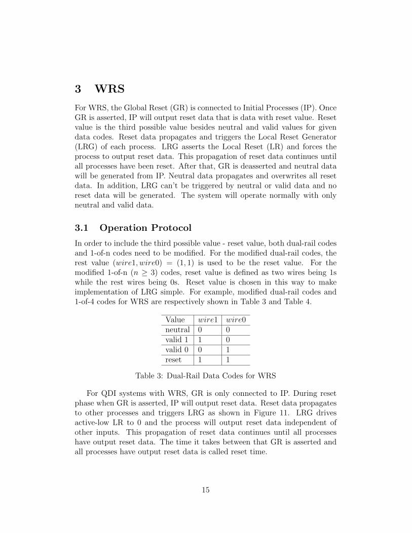
In order to include the third possible value - reset value, both dual-rail codesand 1-of-n codes need to be modified. For the modified dual-rail codes, therest value (wire1, wire0) = (1, 1) is used to be the reset value. For themodified 1-of-n (n ≥ 3) codes, reset value is defined as two wires being 1swhile the rest wires being 0s. Reset value is chosen in this way to makeimplementation of LRG simple. For example, modified dual-rail codes and1-of-4 codes for WRS are respectively shown in Table 3 and Table 4.
Value wire1 wire0neutral 0 0valid 1 1 0valid 0 0 1reset 1 1
Table 3: Dual-Rail Data Codes for WRS
For QDI systems with WRS, GR is only connected to IP. During resetphase when GR is asserted, IP will output reset data. Reset data propagatesto other processes and triggers LRG as shown in Figure 11. LRG drivesactive-low LR to 0 and the process will output reset data independent ofother inputs. This propagation of reset data continues until all processeshave output reset data. The time it takes between that GR is asserted andall processes have output reset data is called reset time.
15
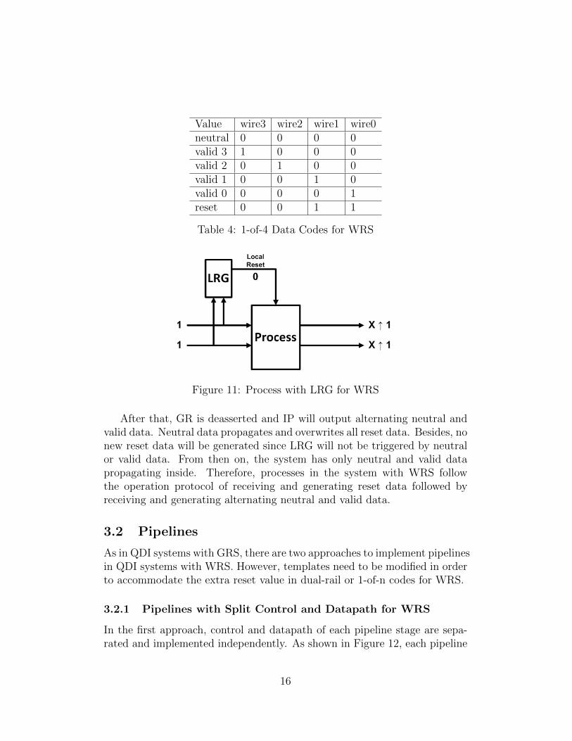
Value wire3 wire2 wire1 wire0neutral 0 0 0 0valid 3 1 0 0 0valid 2 0 1 0 0valid 1 0 0 1 0valid 0 0 0 0 1reset 0 0 1 1
Table 4: 1-of-4 Data Codes for WRS
Figure 11: Process with LRG for WRS
After that, GR is deasserted and IP will output alternating neutral andvalid data. Neutral data propagates and overwrites all reset data. Besides, nonew reset data will be generated since LRG will not be triggered by neutralor valid data. From then on, the system has only neutral and valid datapropagating inside. Therefore, processes in the system with WRS followthe operation protocol of receiving and generating reset data followed byreceiving and generating alternating neutral and valid data.
3.2 Pipelines
As in QDI systems with GRS, there are two approaches to implement pipelinesin QDI systems with WRS. However, templates need to be modified in orderto accommodate the extra reset value in dual-rail or 1-of-n codes for WRS.
3.2.1 Pipelines with Split Control and Datapath for WRS
In the first approach, control and datapath of each pipeline stage are sepa-rated and implemented independently. As shown in Figure 12, each pipeline
16
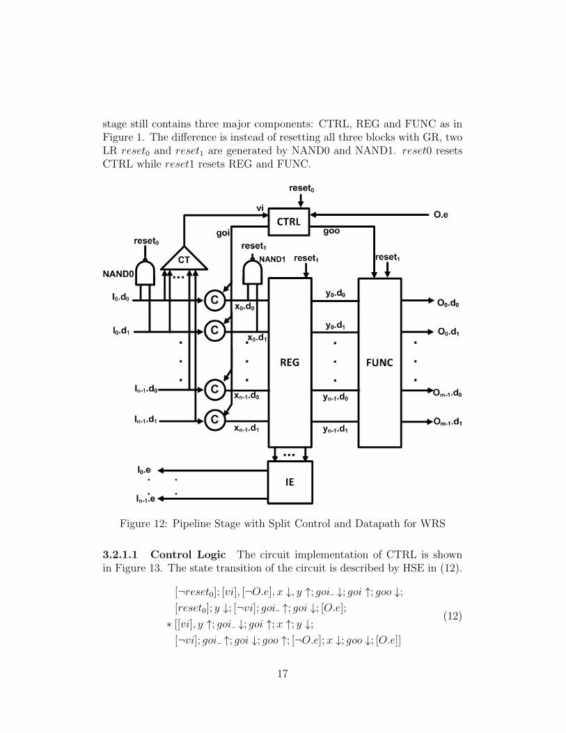
stage still contains three major components: CTRL, REG and FUNC as inFigure 1. The difference is instead of resetting all three blocks with GR, twoLR reset0 and reset1 are generated by NAND0 and NAND1. reset0 resetsCTRL while reset1 resets REG and FUNC.
Figure 12: Pipeline Stage with Split Control and Datapath for WRS
3.2.1.1 Control Logic The circuit implementation of CTRL is shownin Figure 13. The state transition of the circuit is described by HSE in (12).
[¬reset0]; [vi], [¬O.e], x ↓, y ↑; goi ↓; goi ↑; goo ↓;[reset0]; y ↓; [¬vi]; goi ↑; goi ↓; [O.e];
∗ [[vi], y ↑; goi ↓; goi ↑;x ↑; y ↓;[¬vi]; goi ↑; goi ↓; goo ↑; [¬O.e];x ↓; goo ↓; [O.e]]
(12)
17
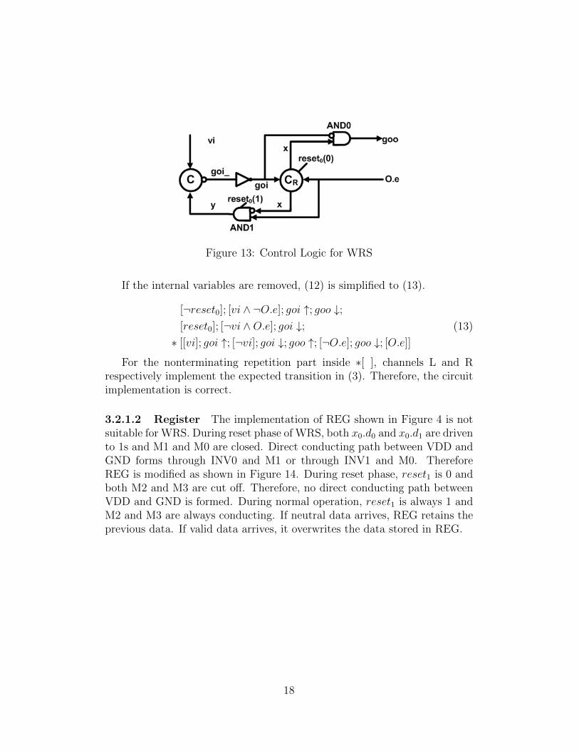
Figure 13: Control Logic for WRS
If the internal variables are removed, (12) is simplified to (13).
[¬reset0]; [vi ∧ ¬O.e]; goi ↑; goo ↓;[reset0]; [¬vi ∧O.e]; goi ↓;∗ [[vi]; goi ↑; [¬vi]; goi ↓; goo ↑; [¬O.e]; goo ↓; [O.e]]
(13)
For the nonterminating repetition part inside ∗[ ], channels L and Rrespectively implement the expected transition in (3). Therefore, the circuitimplementation is correct.
3.2.1.2 Register The implementation of REG shown in Figure 4 is notsuitable for WRS. During reset phase of WRS, both x0.d0 and x0.d1 are drivento 1s and M1 and M0 are closed. Direct conducting path between VDD andGND forms through INV0 and M1 or through INV1 and M0. ThereforeREG is modified as shown in Figure 14. During reset phase, reset1 is 0 andboth M2 and M3 are cut off. Therefore, no direct conducting path betweenVDD and GND is formed. During normal operation, reset1 is always 1 andM2 and M3 are always conducting. If neutral data arrives, REG retains theprevious data. If valid data arrives, it overwrites the data stored in REG.
18
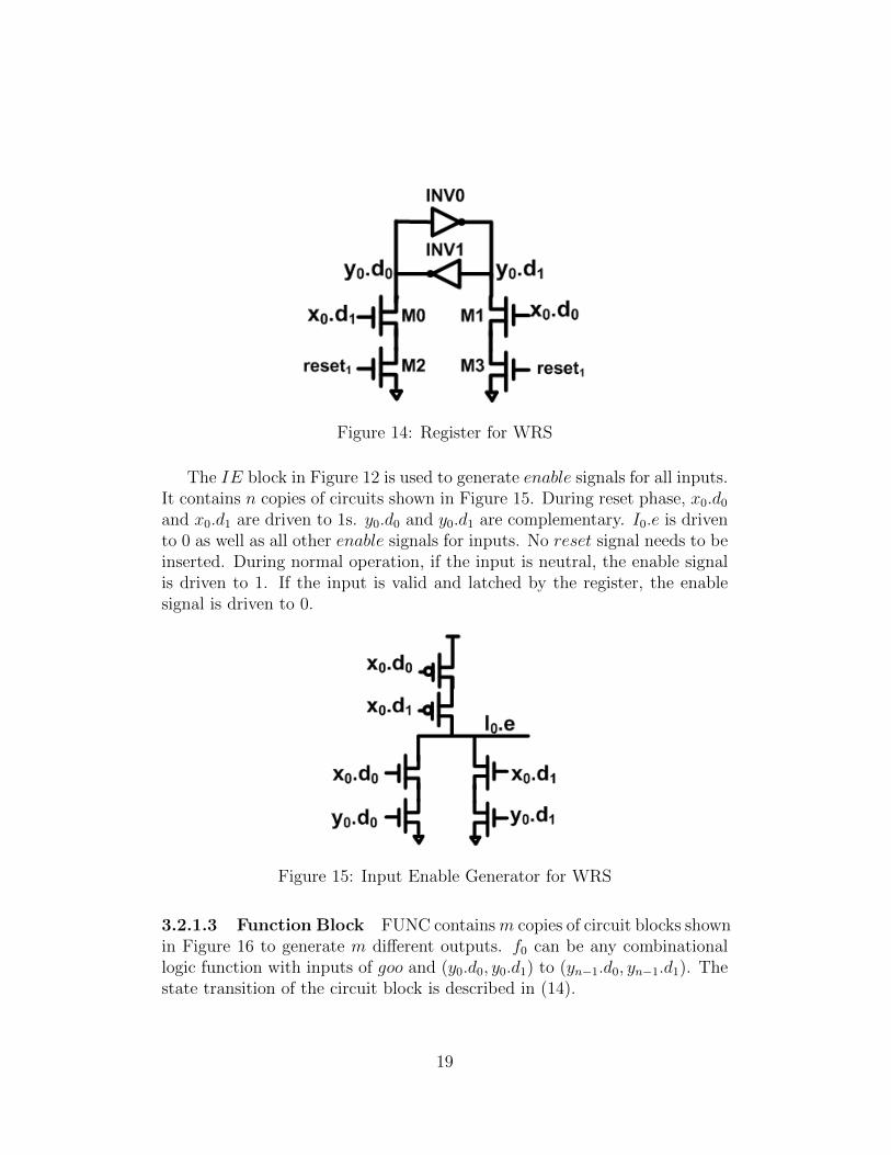
Figure 14: Register for WRS
The IE block in Figure 12 is used to generate enable signals for all inputs.It contains n copies of circuits shown in Figure 15. During reset phase, x0.d0and x0.d1 are driven to 1s. y0.d0 and y0.d1 are complementary. I0.e is drivento 0 as well as all other enable signals for inputs. No reset signal needs to beinserted. During normal operation, if the input is neutral, the enable signalis driven to 1. If the input is valid and latched by the register, the enablesignal is driven to 0.
Figure 15: Input Enable Generator for WRS
3.2.1.3 Function Block FUNC contains m copies of circuit blocks shownin Figure 16 to generate m different outputs. f0 can be any combinationallogic function with inputs of goo and (y0.d0, y0.d1) to (yn−1.d0, yn−1.d1). Thestate transition of the circuit block is described in (14).
19
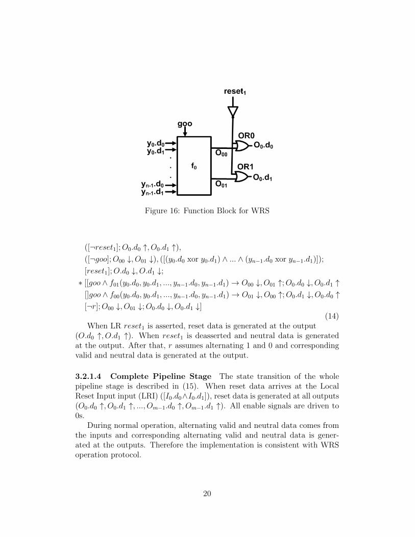
Figure 16: Function Block for WRS
([¬reset1];O0.d0 ↑, O0.d1 ↑),([¬goo];O00 ↓, O01 ↓), ([(y0.d0 xor y0.d1) ∧ ... ∧ (yn−1.d0 xor yn−1.d1)]);
[reset1];O.d0 ↓, O.d1 ↓;∗ [[goo ∧ f01(y0.d0, y0.d1, ..., yn−1.d0, yn−1.d1)→ O00 ↓, O01 ↑;O0.d0 ↓, O0.d1 ↑
[]goo ∧ f00(y0.d0, y0.d1, ..., yn−1.d0, yn−1.d1)→ O01 ↓, O00 ↑;O0.d1 ↓, O0.d0 ↑[¬r];O00 ↓, O01 ↓;O0.d0 ↓, O0.d1 ↓]
(14)When LR reset1 is asserted, reset data is generated at the output
(O.d0 ↑, O.d1 ↑). When reset1 is deasserted and neutral data is generatedat the output. After that, r assumes alternating 1 and 0 and correspondingvalid and neutral data is generated at the output.
3.2.1.4 Complete Pipeline Stage The state transition of the wholepipeline stage is described in (15). When reset data arrives at the LocalReset Input input (LRI) ([I0.d0∧I0.d1]), reset data is generated at all outputs(O0.d0 ↑, O0.d1 ↑, ..., Om−1.d0 ↑, Om−1.d1 ↑). All enable signals are driven to0s.
During normal operation, alternating valid and neutral data comes fromthe inputs and corresponding alternating valid and neutral data is gener-ated at the outputs. Therefore the implementation is consistent with WRSoperation protocol.
20
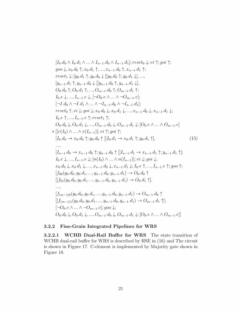
[I0.d0 ∧ I0.d1 ∧ ... ∧ In−1.d0 ∧ In−1.d1]; reset0 ↓; vi ↑; goi ↑;goo ↓, x0.d0 ↑, x0.d1 ↑, ..., xn−1.d0 ↑, xn−1.d1 ↑;reset1 ↓; [y0.d1 ↑, y0.d0 ↓ []y0.d0 ↑, y0.d1 ↓], ...,[yn−1.d1 ↑, yn−1.d0 ↓ []yn−1.d0 ↑, yn−1.d1 ↓],O0.d0 ↑, O0.d1 ↑, ..., Om−1.d0 ↑, Om−1.d1 ↑;I0.e ↓, ..., In−1.e ↓, [¬O0.e ∧ ... ∧ ¬Om−1.e];
[¬I.d0 ∧ ¬I.d1 ∧ ... ∧ ¬In−1.d0 ∧ ¬In−1.d1];reset0 ↑, vi ↓; goi ↓;x0.d0 ↓, x0.d1 ↓, ..., xn−1.d0 ↓, xn−1.d1 ↓;I0.e ↑, ..., In−1.e ↑; reset1 ↑;O0.d0 ↓, O0.d1 ↓, ..., Om−1.d0 ↓, Om−1.d1 ↓; [O0.e ∧ ... ∧Om−1.e]
∗ [[v(I0) ∧ ... ∧ v(In−1)]; vi ↑; goi ↑;[I0.d0 → x0.d0 ↑; y0.d0 ↑ []I0.d1 → x0.d1 ↑; y0.d1 ↑],...,
[In−1.d0 → xn−1.d0 ↑; yn−1.d0 ↑ []In−1.d1 → xn−1.d1 ↑; yn−1.d1 ↑];I0.e ↓, ..., In−1.e ↓; [n(I0) ∧ ... ∧ n(In−1)]; vi ↓; goi ↓;x0.d0 ↓, x0.d1 ↓, ..., xn−1.d0 ↓, xn−1.d1 ↓; I0.e ↑, ..., In−1.e ↑; goo ↑;[f00(y0.d0, y0.d1, ..., yn−1.d0, yn−1.d1)→ O0.d0 ↑[]f01(y0.d0, y0.d1, ..., yn−1.d0, yn−1.d1)→ O0.d1 ↑],...,
[f(m−1)0(y0.d0, y0.d1, ..., yn−1.d0, yn−1.d1)→ Om−1.d0 ↑[]f(m−1)1(y0.d0, y0.d1, ..., yn−1.d0, yn−1.d1)→ Om−1.d1 ↑];[¬O0.e ∧ ... ∧ ¬Om−1.e]; goo ↓;O0.d0 ↓, O0.d1 ↓, ..., Om−1.d0 ↓, Om−1.d1 ↓; [O0.e ∧ ... ∧Om−1.e]]
(15)
3.2.2 Fine-Grain Integrated Pipelines for WRS
3.2.2.1 WCHB Dual-Rail Buffer for WRS The state transition ofWCHB dual-rail buffer for WRS is described by HSE in (16) and The circuitis shown in Figure 17. C-element is implemented by Majority gate shown inFigure 18.
21
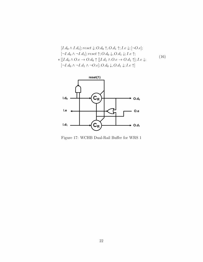
[I.d0 ∧ I.d1]; reset ↓;O.d0 ↑, O.d1 ↑; I.e ↓; [¬O.e];
[¬I.d0 ∧ ¬I.d1]; reset ↑;O.d0 ↓, O.d1 ↓; I.e ↑;∗ [[I.d0 ∧O.e→ O.d0 ↑ []I.d1 ∧O.e→ O.d1 ↑]; I.e ↓;
[¬I.d0 ∧ ¬I.d1 ∧ ¬O.e];O.d0 ↓, O.d1 ↓; I.e ↑]
(16)
Figure 17: WCHB Dual-Rail Buffer for WRS 1
22
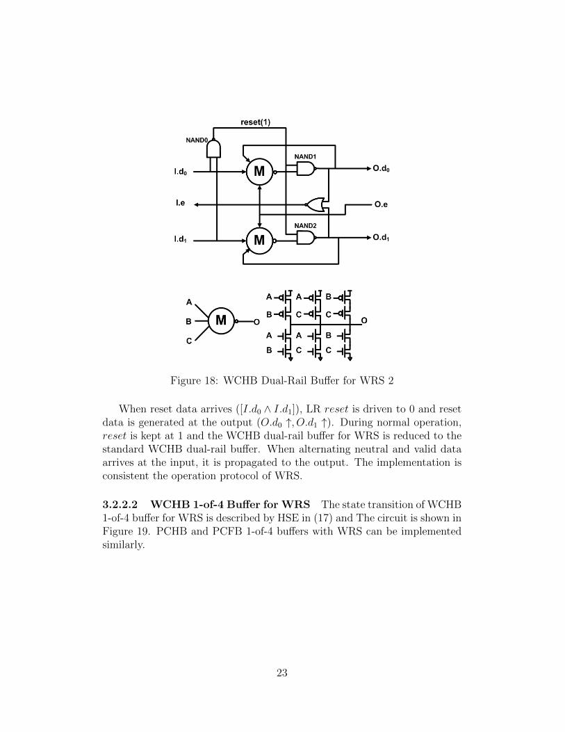
Figure 18: WCHB Dual-Rail Buffer for WRS 2
When reset data arrives ([I.d0 ∧ I.d1]), LR reset is driven to 0 and resetdata is generated at the output (O.d0 ↑, O.d1 ↑). During normal operation,reset is kept at 1 and the WCHB dual-rail buffer for WRS is reduced to thestandard WCHB dual-rail buffer. When alternating neutral and valid dataarrives at the input, it is propagated to the output. The implementation isconsistent the operation protocol of WRS.
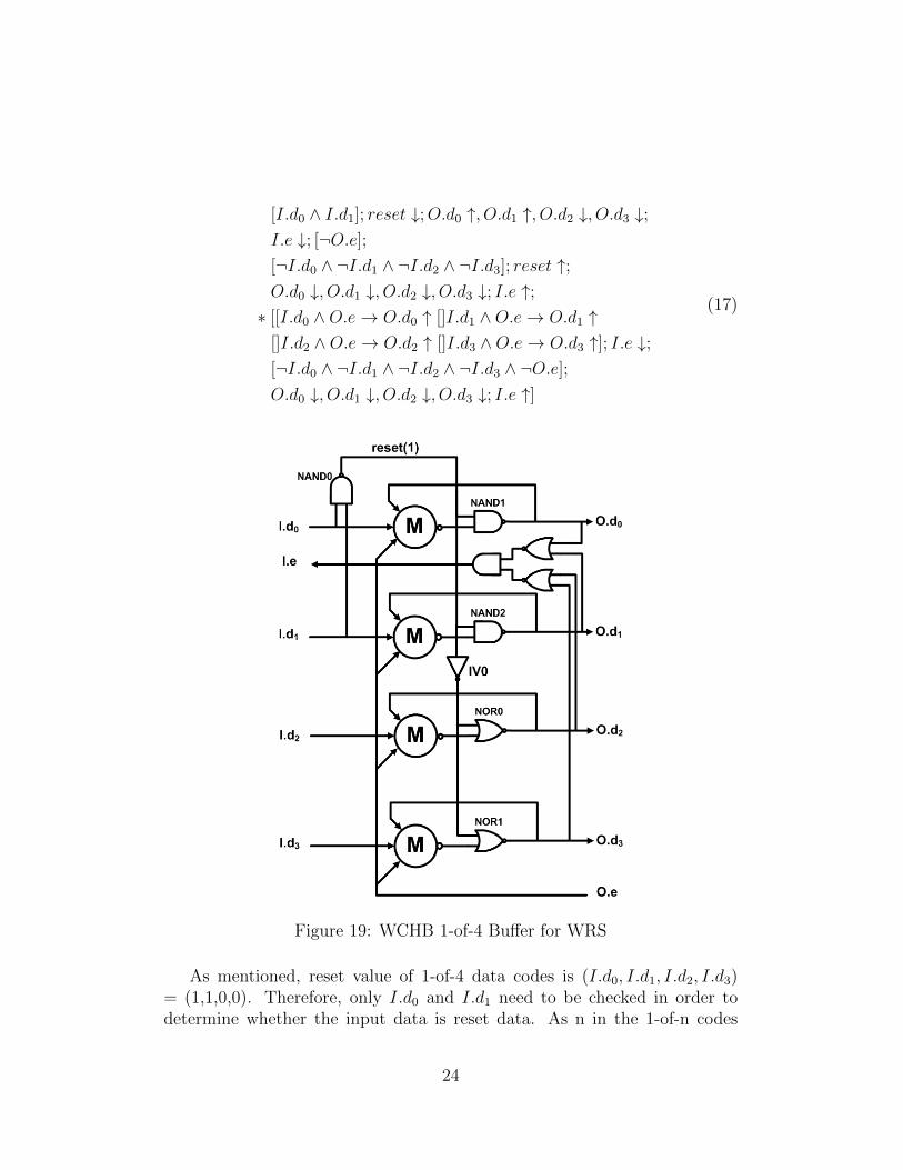
3.2.2.2 WCHB 1-of-4 Buffer for WRS The state transition of WCHB1-of-4 buffer for WRS is described by HSE in (17) and The circuit is shown inFigure 19. PCHB and PCFB 1-of-4 buffers with WRS can be implementedsimilarly.
23
[I.d0 ∧ I.d1]; reset ↓;O.d0 ↑, O.d1 ↑, O.d2 ↓, O.d3 ↓;I.e ↓; [¬O.e];
[¬I.d0 ∧ ¬I.d1 ∧ ¬I.d2 ∧ ¬I.d3]; reset ↑;O.d0 ↓, O.d1 ↓, O.d2 ↓, O.d3 ↓; I.e ↑;∗ [[I.d0 ∧O.e→ O.d0 ↑ []I.d1 ∧O.e→ O.d1 ↑
[]I.d2 ∧O.e→ O.d2 ↑ []I.d3 ∧O.e→ O.d3 ↑]; I.e ↓;[¬I.d0 ∧ ¬I.d1 ∧ ¬I.d2 ∧ ¬I.d3 ∧ ¬O.e];
O.d0 ↓, O.d1 ↓, O.d2 ↓, O.d3 ↓; I.e ↑]
(17)
Figure 19: WCHB 1-of-4 Buffer for WRS
As mentioned, reset value of 1-of-4 data codes is (I.d0, I.d1, I.d2, I.d3)= (1,1,0,0). Therefore, only I.d0 and I.d1 need to be checked in order todetermine whether the input data is reset data. As n in the 1-of-n codes
24
increases, the overhead of LRG remains the same. This is why reset value ischosen as 2 wires being 1s while the rest wires being 0s.
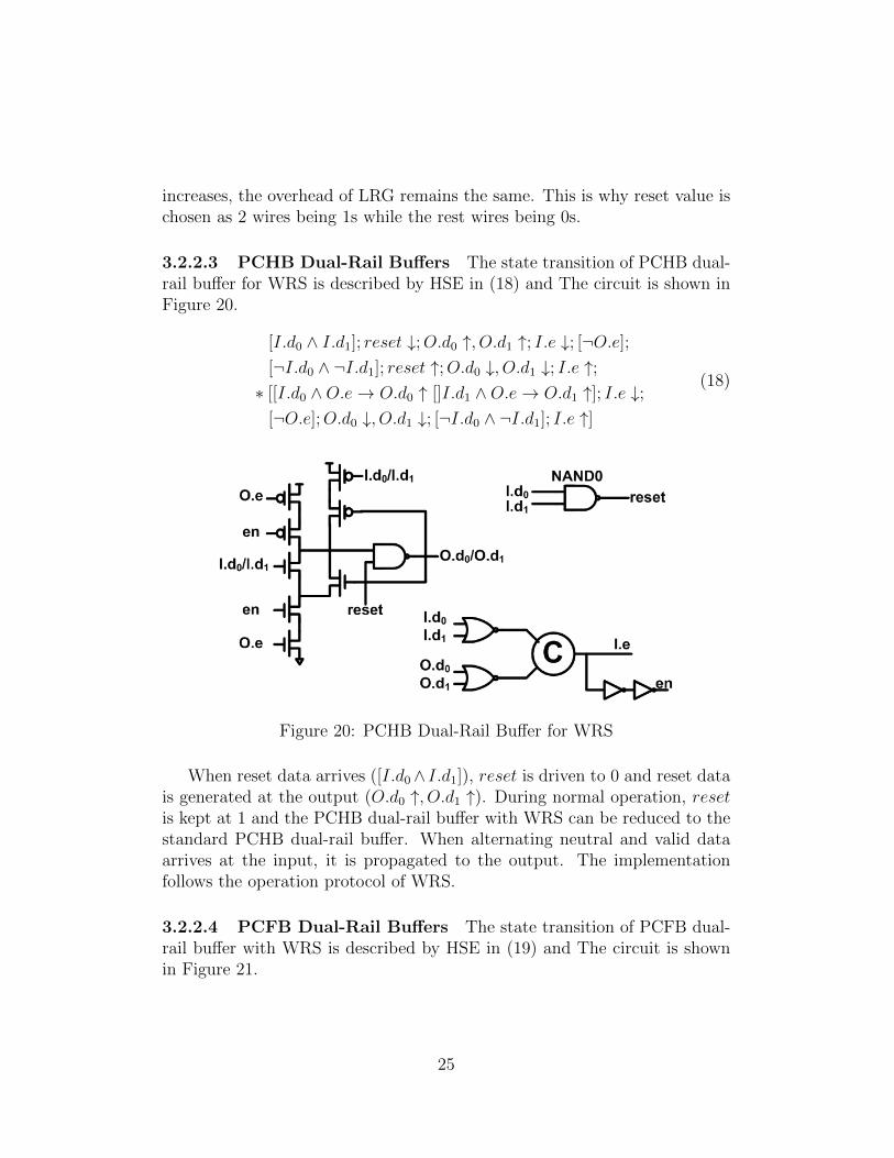
3.2.2.3 PCHB Dual-Rail Buffers The state transition of PCHB dual-rail buffer for WRS is described by HSE in (18) and The circuit is shown inFigure 20.
[I.d0 ∧ I.d1]; reset ↓;O.d0 ↑, O.d1 ↑; I.e ↓; [¬O.e];
[¬I.d0 ∧ ¬I.d1]; reset ↑;O.d0 ↓, O.d1 ↓; I.e ↑;∗ [[I.d0 ∧O.e→ O.d0 ↑ []I.d1 ∧O.e→ O.d1 ↑]; I.e ↓;
[¬O.e];O.d0 ↓, O.d1 ↓; [¬I.d0 ∧ ¬I.d1]; I.e ↑]
(18)
Figure 20: PCHB Dual-Rail Buffer for WRS
When reset data arrives ([I.d0∧ I.d1]), reset is driven to 0 and reset datais generated at the output (O.d0 ↑, O.d1 ↑). During normal operation, resetis kept at 1 and the PCHB dual-rail buffer with WRS can be reduced to thestandard PCHB dual-rail buffer. When alternating neutral and valid dataarrives at the input, it is propagated to the output. The implementationfollows the operation protocol of WRS.
3.2.2.4 PCFB Dual-Rail Buffers The state transition of PCFB dual-rail buffer with WRS is described by HSE in (19) and The circuit is shownin Figure 21.
25
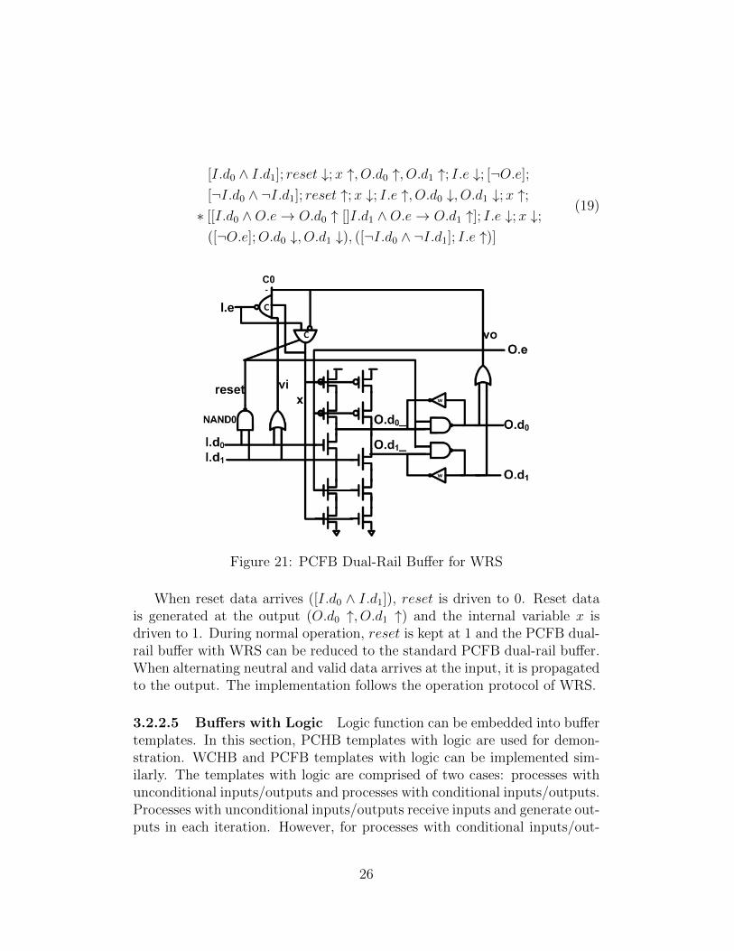
[I.d0 ∧ I.d1]; reset ↓;x ↑, O.d0 ↑, O.d1 ↑; I.e ↓; [¬O.e];
[¬I.d0 ∧ ¬I.d1]; reset ↑;x ↓; I.e ↑, O.d0 ↓, O.d1 ↓;x ↑;∗ [[I.d0 ∧O.e→ O.d0 ↑ []I.d1 ∧O.e→ O.d1 ↑]; I.e ↓;x ↓;
([¬O.e];O.d0 ↓, O.d1 ↓), ([¬I.d0 ∧ ¬I.d1]; I.e ↑)]
(19)
Figure 21: PCFB Dual-Rail Buffer for WRS
When reset data arrives ([I.d0 ∧ I.d1]), reset is driven to 0. Reset datais generated at the output (O.d0 ↑, O.d1 ↑) and the internal variable x isdriven to 1. During normal operation, reset is kept at 1 and the PCFB dual-rail buffer with WRS can be reduced to the standard PCFB dual-rail buffer.When alternating neutral and valid data arrives at the input, it is propagatedto the output. The implementation follows the operation protocol of WRS.
3.2.2.5 Buffers with Logic Logic function can be embedded into buffertemplates. In this section, PCHB templates with logic are used for demon-stration. WCHB and PCFB templates with logic can be implemented sim-ilarly. The templates with logic are comprised of two cases: processes withunconditional inputs/outputs and processes with conditional inputs/outputs.Processes with unconditional inputs/outputs receive inputs and generate out-puts in each iteration. However, for processes with conditional inputs/out-
26
puts, depending on values of some inputs, they may or may not receive otherinputs or generate outputs.
Processes with unconditional inputs/outputs can be described by CHPin (20), where I0, I1, ..., In−1 are n inputs, O0, O1, ..., Om−1 are m outputs,X is the set of all variables {x0, x1, ...xn−1}, f0, f1, ..., fm−1 are functions togenerate O0, O1, ..., Om−1. In each iteration, processes with unconditionalinputs/outputs always receive data from all inputs, apply functions to thedata and send results through outputs.
∗[I0?x0, I1?x1, ..., In−1?xn−1;O0!f0(X), O1!f1(X), ..., Om−1!fm−1(X)] (20)
It is assumed I0 is LRI. The choice of LRI will be discussed in Chapter4. All inputs/outputs are assumed to be dual-rail encoded. (Processes withother 1-of-n data encoding can be similarly implemented). The process withunconditional inputs/outputs is implemented with PCHB templates in (21).
i ∈ [0..n− 1]
j ∈ [0..m− 1]
I0.d0 ∧ I0.d1 → reset ↓¬I0.d0 ∨ ¬I0.d1 → reset ↑
reset ∧ ¬Oj.e ∧ ¬enj → Oj.d0 ↓reset ∧ ¬Oj.e ∧ ¬enj → Oj.d1 ↓
¬reset ∨ (Oj.e ∧ enj ∧ fj0({Ii.d0, Ii.d1})→ Oj.d0 ↑¬reset ∨ (Oj.e ∧ enj ∧ fj1({Ii.d0, Ii.d1)} → Oj.d1 ↑
¬Ii.d0 ∧ ¬Ii.d1 → vIi ↓Ii.d0 ∨ Ii.d1 → vIi ↑
¬Oj.d0 ∧ ¬Oj.d1 → vOj ↓Oj.d0 ∨Oj.d1 → vOj ↑
vIi ∧ ({∧h∈[0,m−1]|Ohdepends on Ii
vOh})→ Ii.e ↓
¬vIi ∧ ({∧h∈[0,m−1]|Ohdepends on Ii
¬vOh})→ Ii.e ↑
vOj ∧ ({∧k∈[0,n−1]|Ojdepends on Ik
vIk})→ enj ↓
¬vOj ∧ ({∧k∈[0,n−1]|Ojdepends on Ik
¬vIk})→ enj ↑
(21)
The variables vIi and vOj refer to the validity of input Ii and outputOj. For example, when input I0 has reset or valid data (I0.d0 ∨ I0.d1 = 1),vI0 = 1. When input I0 has neutral data (I0.d0 = I0.d1 = 0), vI0 = 0.
27
fj0({Ii.d0, Ii.d1}) and fj1({Ii.d0, Ii.d1}) respectively generate valid outputOj.d0 and Oj.d1 based on subset of inputs. In order to acknowledge Ii(Ii.e ↓/Ii.e ↑), the validity of the input itself as well as all the outputs thatdepend on the input must be 1/0. For example, if O0, O2 and O3 are threeoutputs that depend on I0, I0.e is generated as shown in (22).
vI0 ∧ vO0 ∧ vO2 ∧ vO3 → I0.e ↓¬vI0 ∧ ¬vO0 ∧ ¬vO2 ∧ ¬vO3 → I0.e ↑
(22)
Similarly, in order to generate enable signal enj (enj−/enj ↑), the validityof the output as well as all the inputs that the output is dependent on mustbe 1/0.
Processes with conditional inputs/outputs can be described in (23). Thereare n condition inputs Ci, k conditions that are function of Ci, m data inputsIj and p outputs Oh. The process receives condition inputs in each iteration.Based on values of condition inputs, it determines which condition amongcond0, cond1, ..., condk−1 is true. Based on the true condition, it selectivelyreceives data from some inputs, computes functions on the received data andsends results through some outputs.
∗ [{Ci?ci|i∈[0,n−1], };[cond0 → {Ij0?dj0|j0∈[0,m−1], }; {Oh0 !fh0|h0∈[0,p−1], };[]cond1 → {Ij1?dj1|j1∈[0,m−1], }; {Oh1 !fh1|h1∈[0,p−1], };.
.
.
[]condk−1 → {Ijk−1?djk−1
|jk−1∈[0,m−1], }; {Ohk−1!fhk−1
|hk−1∈[0,p−1], };]]
(23)
Processes with conditional inputs/outputs can be implemented as shownin (24). It is assumed I0 is LRI. condu is a function gu() of condition in-puts. For example, if there are two condition inputs and gu() is logic AND,gu({c0, c1}) = c0∧c1. The variables vIj and vOh refer to the validity of inputIj and output Oh. fhf
({cdu, Ij.d0, Ij.d1}) and fht({cdu, Ij.d0, Ij.d1}) respec-tively generate outputs Oh.d0 and Oh.d1 based on conditions and subset ofinputs. In order to acknowledge Ij (Ij.e ↓/Ij.e ↑), the conditions inside whichIj exists are first determined. If in any condition, the condition, validity of Ijand validity of all outputs that depend on Ij are 1s, Ij.e is driven to 0. Whenall conditions, validity of Ij and validity of outputs that depend on Ij are 0s,
28
Ij.e is driven to 1. Similarly for enh, if in any condition where Oh exists, thecondition, validity of Oh and validity of all inputs that Oh depends on are1s, enh is driven to 0. If for all conditions where Oh exists, the conditions,validity of Oh and validity of inputs that Oh depends on are 0s, enh is drivento 1.
For both processes with conditional/unconditional inputs/outputs, dur-ing reset phase, reset data arrives at different inputs at different time. Whenreset data arrives at inputs other than LRI I0, garbage data may be gener-ated at outputs. However, once reset data arrives at I0, LR reset is drivento 0 and reset data is generated at all outputs. The transition from garbagedata to reset data is monotonic during reset phase; that is, the garbage dataat the outputs will be overwritten by reset data and reset data will remainthrough the whole reset phase. Therefore, given enough time, reset data cantraverse the whole system and every process in the system will generate resetdata at its output. All validity signals are driven to 1s and all I.e and en aredriven to 0s.
GR is then deasserted and IP starts to generate neutral data. Like resetdata, neutral data arrives at different inputs at different time. If neutral datahasn’t arrived at I0, reset data remains at the outputs no matter whetherneutral data has arrived at other inputs. When neutral data arrives at I0,reset is driven to 1. At this moment, O.e and en are still 0s because outputshaven’t changed from reset data yet. Therefore all the outputs will generateneutral data. If some inputs still have reset data, they will not accidentallygenerate wrong data at the output. It is because when an input I has resetdata, vI is 1. I.e and all en that depends on vI are still 0s. Neutral dataremains at the relevant outputs. Given enough time, all reset data will beoverwritten by neutral data. LRG keeps LR at 0 and no reset data will begenerated any more. Processes operate normally with alternating neutraland valid data.
29
i ∈ [0, n− 1]
j ∈ [0,m− 1]
h ∈ [0, p− 1]
u ∈ [0, k − 1]
I0.d0 ∧ I0.d1 → reset ↓¬I0.d0 ∨ ¬I0.d1 → reset ↑
gu({ci})→ condu ↑¬condu → condu ↓
¬Ij.d0 ∧ ¬Ij.d1 → vIj ↓Ij.d0 ∨ Ij.d1 → vIj ↑
¬Oh.d0 ∧ ¬Oh.d1 → vOh ↓Oh.d0 ∨Oh.d1 → vOh ↑
{∨u|Ij in condu(condu ∧ vIj ∧ ({∧h∈[0,m−1]|Ohu depends on IjvOhu}))} → Ij.e ↓{∧u|Ij in condu(¬condu ∧ ¬vIj ∧ ({∧h∈[0,m−1]|Ohu depends on Ij¬vOhu}))} → Ij.e ↑{∨u|Oh in condu(condu ∧ vOh ∧ ({∧k∈[0,n−1]|Oh depends on Iju
vIju}))} → enh ↓{∧u|Oh in condu(¬condu ∧ ¬vOh ∧ ({∧k∈[0,n−1]|Oh depends on Iju
¬vIju}))} → enh ↑reset ∧ ¬Oh.e ∧ ¬enh → Oh.d0 ↓reset ∧ ¬Oh.e ∧ ¬enh → Oh.d1 ↓
¬reset ∨ (Oh.e ∧ enh ∧ fhf({cdu, Ij.d0, Ij.d1})→ Oh.d0 ↑
¬reset ∨ (Oh.e ∧ enh ∧ fht({cdu, Ij.d0, Ij.d1})→ Oh.d1 ↑(24)
30
3.3 Special Blocks
Besides processes described in (2), there are other special processes withdifferent CHP description and must be implemented separately.
3.3.1 Source/Sink
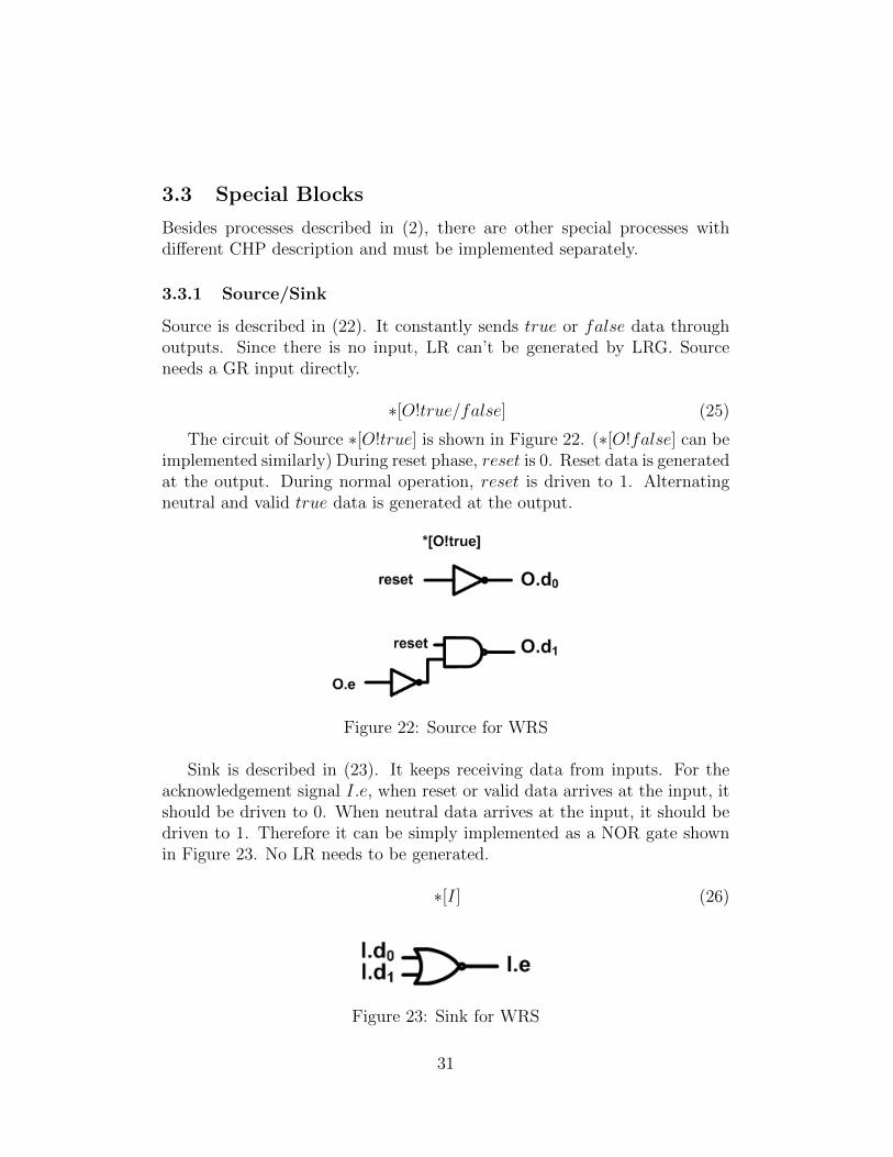
Source is described in (22). It constantly sends true or false data throughoutputs. Since there is no input, LR can’t be generated by LRG. Sourceneeds a GR input directly.
∗[O!true/false] (25)
The circuit of Source ∗[O!true] is shown in Figure 22. (∗[O!false] can beimplemented similarly) During reset phase, reset is 0. Reset data is generatedat the output. During normal operation, reset is driven to 1. Alternatingneutral and valid true data is generated at the output.
Figure 22: Source for WRS
Sink is described in (23). It keeps receiving data from inputs. For theacknowledgement signal I.e, when reset or valid data arrives at the input, itshould be driven to 0. When neutral data arrives at the input, it should bedriven to 1. Therefore it can be simply implemented as a NOR gate shownin Figure 23. No LR needs to be generated.
∗[I] (26)
Figure 23: Sink for WRS
31
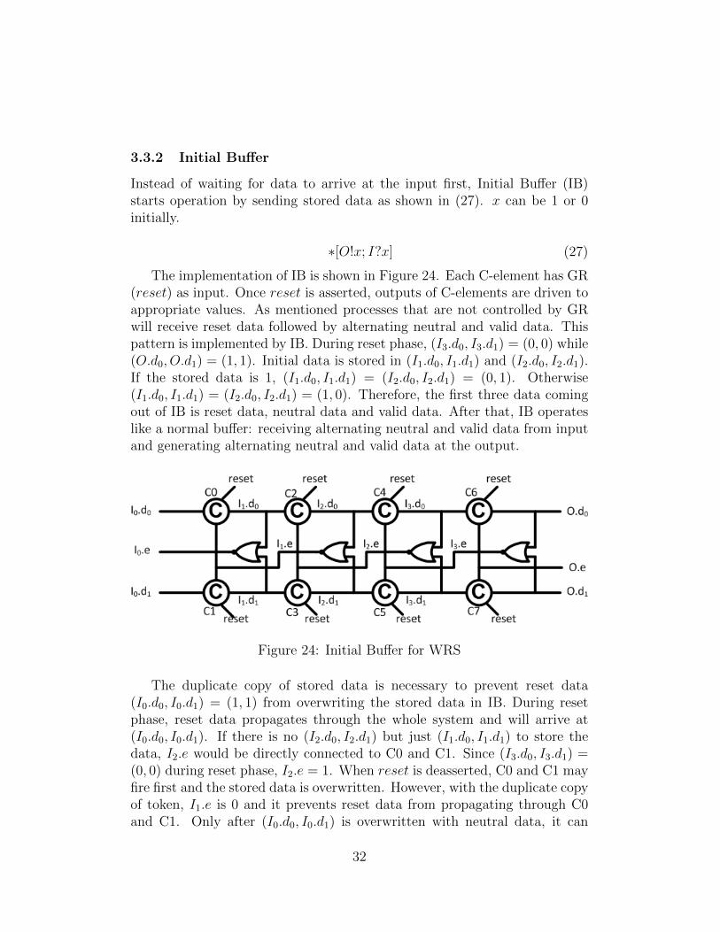
3.3.2 Initial Buffer
Instead of waiting for data to arrive at the input first, Initial Buffer (IB)starts operation by sending stored data as shown in (27). x can be 1 or 0initially.
∗[O!x; I?x] (27)
The implementation of IB is shown in Figure 24. Each C-element has GR(reset) as input. Once reset is asserted, outputs of C-elements are driven toappropriate values. As mentioned processes that are not controlled by GRwill receive reset data followed by alternating neutral and valid data. Thispattern is implemented by IB. During reset phase, (I3.d0, I3.d1) = (0, 0) while(O.d0, O.d1) = (1, 1). Initial data is stored in (I1.d0, I1.d1) and (I2.d0, I2.d1).If the stored data is 1, (I1.d0, I1.d1) = (I2.d0, I2.d1) = (0, 1). Otherwise(I1.d0, I1.d1) = (I2.d0, I2.d1) = (1, 0). Therefore, the first three data comingout of IB is reset data, neutral data and valid data. After that, IB operateslike a normal buffer: receiving alternating neutral and valid data from inputand generating alternating neutral and valid data at the output.
Figure 24: Initial Buffer for WRS
The duplicate copy of stored data is necessary to prevent reset data(I0.d0, I0.d1) = (1, 1) from overwriting the stored data in IB. During resetphase, reset data propagates through the whole system and will arrive at(I0.d0, I0.d1). If there is no (I2.d0, I2.d1) but just (I1.d0, I1.d1) to store thedata, I2.e would be directly connected to C0 and C1. Since (I3.d0, I3.d1) =(0, 0) during reset phase, I2.e = 1. When reset is deasserted, C0 and C1 mayfire first and the stored data is overwritten. However, with the duplicate copyof token, I1.e is 0 and it prevents reset data from propagating through C0and C1. Only after (I0.d0, I0.d1) is overwritten with neutral data, it can
32
overwrite (I1.d0, I1.d1). At that time, the data is kept at (I2.d0, I2.d1). Theneutral data at (I1.d0, I1.d1) will not overwrite (I2.d0, I2.d1) until valid dataat (I2.d0, I2.d1) propagates to (I3.d0, I3.d1). Therefore, reset data startingfrom IB will stop at the input of IB and be overwritten by neutral data.When all reset data has been overwritten, the system correctly transits intonormal operation with only neutral and valid data propagating inside.
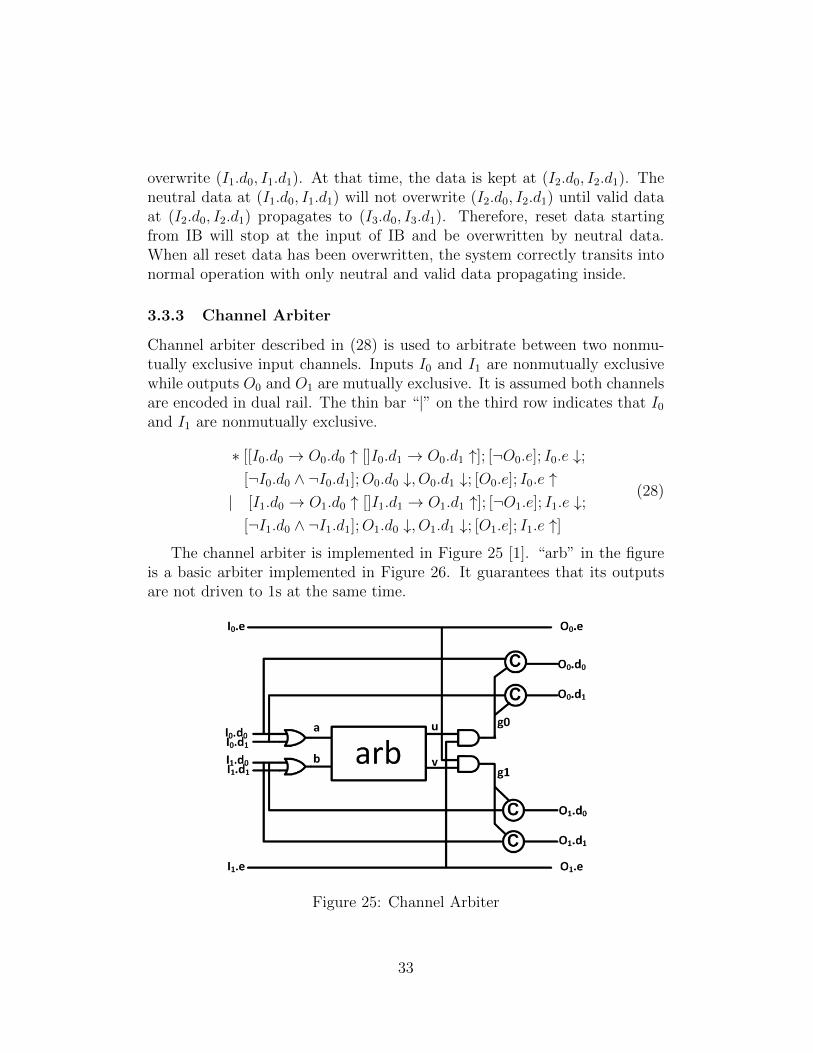
3.3.3 Channel Arbiter
Channel arbiter described in (28) is used to arbitrate between two nonmu-tually exclusive input channels. Inputs I0 and I1 are nonmutually exclusivewhile outputs O0 and O1 are mutually exclusive. It is assumed both channelsare encoded in dual rail. The thin bar “|” on the third row indicates that I0and I1 are nonmutually exclusive.
∗ [[I0.d0 → O0.d0 ↑ []I0.d1 → O0.d1 ↑]; [¬O0.e]; I0.e ↓;[¬I0.d0 ∧ ¬I0.d1];O0.d0 ↓, O0.d1 ↓; [O0.e]; I0.e ↑| [I1.d0 → O1.d0 ↑ []I1.d1 → O1.d1 ↑]; [¬O1.e]; I1.e ↓;
[¬I1.d0 ∧ ¬I1.d1];O1.d0 ↓, O1.d1 ↓; [O1.e]; I1.e ↑]
(28)
The channel arbiter is implemented in Figure 25 [1]. “arb” in the figureis a basic arbiter implemented in Figure 26. It guarantees that its outputsare not driven to 1s at the same time.
Figure 25: Channel Arbiter
33
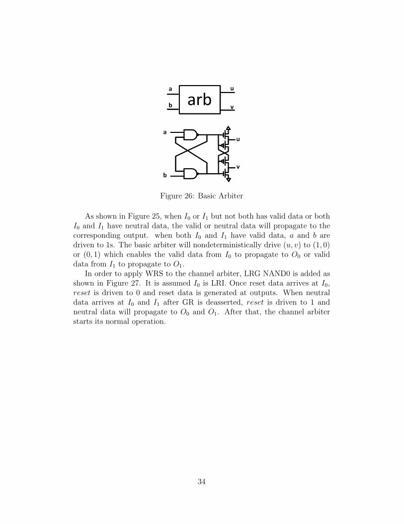
Figure 26: Basic Arbiter
As shown in Figure 25, when I0 or I1 but not both has valid data or bothI0 and I1 have neutral data, the valid or neutral data will propagate to thecorresponding output. when both I0 and I1 have valid data, a and b aredriven to 1s. The basic arbiter will nondeterministically drive (u, v) to (1, 0)or (0, 1) which enables the valid data from I0 to propagate to O0 or validdata from I1 to propagate to O1.
In order to apply WRS to the channel arbiter, LRG NAND0 is added asshown in Figure 27. It is assumed I0 is LRI. Once reset data arrives at I0,reset is driven to 0 and reset data is generated at outputs. When neutraldata arrives at I0 and I1 after GR is deasserted, reset is driven to 1 andneutral data will propagate to O0 and O1. After that, the channel arbiterstarts its normal operation.
34
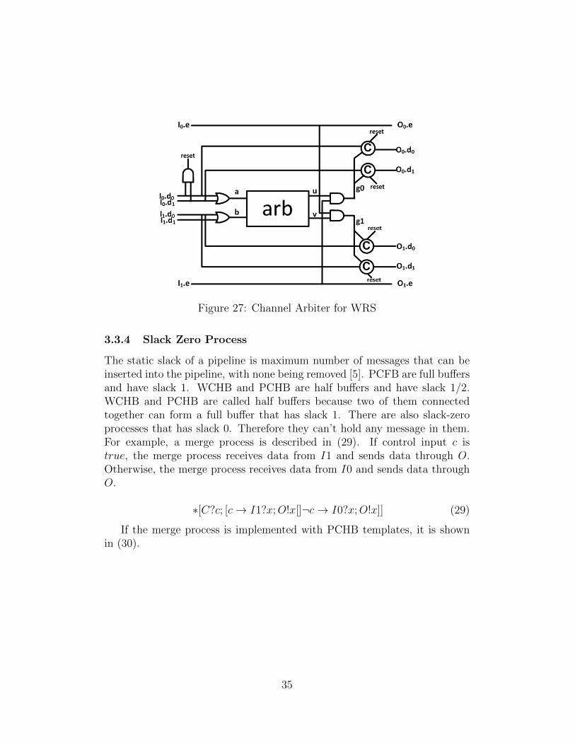
Figure 27: Channel Arbiter for WRS
3.3.4 Slack Zero Process
The static slack of a pipeline is maximum number of messages that can beinserted into the pipeline, with none being removed [5]. PCFB are full buffersand have slack 1. WCHB and PCHB are half buffers and have slack 1/2.WCHB and PCHB are called half buffers because two of them connectedtogether can form a full buffer that has slack 1. There are also slack-zeroprocesses that has slack 0. Therefore they can’t hold any message in them.For example, a merge process is described in (29). If control input c istrue, the merge process receives data from I1 and sends data through O.Otherwise, the merge process receives data from I0 and sends data throughO.
∗[C?c; [c→ I1?x;O!x[]¬c→ I0?x;O!x]] (29)
If the merge process is implemented with PCHB templates, it is shownin (30).
35

I0.d0 ∨ I0.d1 → vI0 ↑¬I0.d0 ∧ ¬I0.d1 → vI0 ↓
I1.d0 ∨ I1.d1 → vI1 ↑¬I1.d0 ∧ ¬I1.d1 → vI1 ↓
O.d0 ∨O.d1 → O ↑¬O.d0 ∧ ¬O.d1 → O ↓vO ∧ C.d0 ∧ vI0 → I0.e ↓
¬vO ∧ ¬C.d0 ∧ ¬vI0 → I0.e ↑vO ∧ C.d1 ∧ vI1 → I1.e ↓
¬vO ∧ ¬C.d1 ∧ ¬vI1 → I1.e ↑I0.e ∧ I1.e→ C.e ↑
¬I0.e ∨ ¬I1.e→ C.e ↓C.e ∧O.e→ en ↑
¬C.e ∧ ¬O.e→ en ↓en ∧ ((C.d0 ∧ I0.d0) ∨ (C.d1 ∧ I1.d0))→ O.d0 ↑
¬en→ O.d0 ↓en ∧ ((C.d0 ∧ I0.d1) ∨ (C.d1 ∧ I1.d1))→ O.d1 ↑
¬en→ O.d1 ↓
(30)
36

If it is implemented with slack-zero processes, it is shown in (31).
I0.d0 ∧ C.d0 → i00c0 ↑¬I0.d0 ∧ ¬C.d0 → i00c0 ↓
I1.d0 ∧ C.d1 → i10c1 ↑¬I1.d0 ∧ ¬C.d1 → i10c1 ↓
I0.d1 ∧ C.d0 → i01c0 ↑¬I0.d1 ∧ ¬C.d0 → i01c0 ↓
I1.d1 ∧ C.d1 → i11c1 ↑¬I1.d1 ∧ ¬C.d1 → i11c1 ↓i00c0 ∨ i10c1→ O.d0 ↑
¬i00c0 ∧ ¬i10c1→ O.d0 ↓i01c0 ∨ i11c1→ O.d1 ↑
¬i01c0 ∧ ¬i11c1→ O.d1 ↓O.e ∧ ¬C.d0 → I0.e ↑¬O.e ∧ C.d0 → I0.e ↓O.e ∧ ¬C.d1 → I1.e ↑¬O.e ∧ C.d1 → I1.e ↓I0.e ∧ I1.e→ C.e ↑
¬I0.e ∨ ¬I1.e→ C.e ↓
(31)
Slack-zero processes don’t introduce any sequence. Whatever arrives atthe input will go through some logic function and the result of which willbe output. True rail and false rail are separately driven to 1 when subset ofinput rails are 1s. Therefore, when all inputs have reset data, i.e. all inputrails are 1s, all output rails are driven to 1s. No LR needs to be generatedfor slack-zero processes.
37
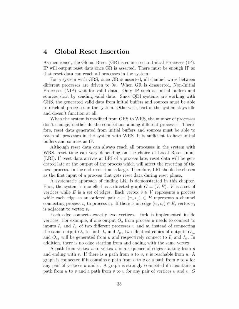
4 Global Reset Insertion
As mentioned, the Global Reset (GR) is connected to Initial Processes (IP).IP will output reset data once GR is asserted. There must be enough IP sothat reset data can reach all processes in the system.
For a system with GRS, once GR is asserted, all channel wires betweendifferent processes are driven to 0s. When GR is deasserted, Non-InitialProcesses (NIP) wait for valid data. Only IP such as initial buffers andsources start by sending valid data. Since QDI systems are working withGRS, the generated valid data from initial buffers and sources must be ableto reach all processes in the system. Otherwise, part of the system stays idleand doesn’t function at all.
When the system is modified from GRS to WRS, the number of processesdon’t change, neither do the connections among different processes. There-fore, reset data generated from initial buffers and sources must be able toreach all processes in the system with WRS. It is sufficient to have initialbuffers and sources as IP.
Although reset data can always reach all processes in the system withWRS, reset time can vary depending on the choice of Local Reset Input(LRI). If reset data arrives at LRI of a process late, reset data will be gen-erated late at the output of the process which will affect the resetting of thenext process. In the end reset time is large. Therefore, LRI should be chosenas the first input of a process that gets reset data during reset phase.
A systematic approach of finding LRI is demonstrated in this chapter.First, the system is modelled as a directed graph G ≡ (V,E). V is a set ofvertices while E is a set of edges. Each vertex v ∈ V represents a processwhile each edge as an ordered pair e ≡ (vi, vj) ∈ E represents a channelconnecting process vi to process vj. If there is an edge (vi, vj) ∈ E, vertex vjis adjacent to vertex vi.
Each edge connects exactly two vertices. Fork is implemented insidevertices. For example, if one output Ou from process u needs to connect toinputs Iv and Iw of two different processes v and w, instead of connectingthe same output Ou to both Iv and Iw, two identical copies of outputs Ou0
and Ou1 will be generated from u and respectively connect to Iv and Iw. Inaddition, there is no edge starting from and ending with the same vertex.
A path from vertex u to vertex v is a sequence of edges starting from uand ending with v. If there is a path from u to v, v is reachable from u. Agraph is connected if it contains a path from u to v or a path from v to u forany pair of vertices u and v. A graph is strongly connected if it contains apath from u to v and a path from v to u for any pair of vertices u and v. G
38
in the QDI systems is connected but not necessarily strongly connected.
4.1 Breadth First Search (BFS)
As introduced in [4], Breadth First Search (BFS) systematically exploresedges of G to discover every vertex that is reachable from the root vertexv. It also generates a Breadth-First Tree (BFT) whose root is v. The treecontains all reachable vertices from v.
The pseudocode of BFS is shown in Figure 28. The algorithm has G andv as inputs. Each vertex in G has two attributes, color and parent. Color isused to distinguish different states of a vertex. Initially all vertices are white.When a vertex is traversed the first time, it becomes gray. If all adjacentvertices of a gray vertex have been traversed, it becomes black. When avertex v is traversed the first time in the course of scanning the adjacentvertices of an already traversed vertex u, u is the parent of v and v is thechild of u.
BFS(G, v) works as follows. Line 2 creates an empty queue Q which isused to store the first-time traversed vertices. Q.enqueue(v) inserts vertexv into Q while Q.dequeue() removes the first element in Q and returns it.Line 3 creates an empty tree T . T.add(u, v) inserts v into T as the child ofu. After the execution of the algorithm, T is BFT. Line 4-6 mark all verticeswhite and set their parent NIL. The root vertex v is first marked gray andadded into T and Q as in Line 7-9. The while loop in Line 10-18 iterates aslong as Q is not empty. During each iteration, the first element n is removedfrom Q. If any of its adjacent vertices s is white which indicates s hasn’tbeen traversed, s will be marked gray and s’s parent is set to n. s is theninserted into T and Q. When all its adjacent vertices have been traversed, nis marked black.
4.2 Breadth First Search with Multiple Roots (BF-SMR)
In order to find LRI in a QDI system with WRS, BFS is run to generate aBFT. The edges in the BFT are LRI of child vertices. Normally, there aremore than one IP in the QDI system with WRS, BFS is modified to BFSMRthat starts the search with multiple roots. Correspondingly, instead of BFT,Breadth-First Forest (BFF) is generated. Edges in BFF are LRI of childvertices. All processes represented by the roots are directly controlled byGR.
39
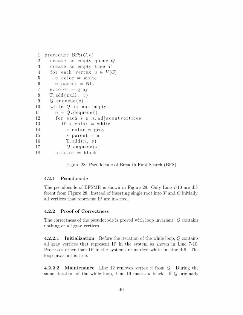
1 procedure BFS(G, v )2 c r e a t e an empty queue Q3 c r e a t e an empty t r e e T4 f o r each ver tex u ∈ V (G)5 u . c o l o r = white6 u . parent = NIL7 v . c o l o r = gray8 T. add ( nu l l , v )9 Q . enqueue (v )
10 whi l e Q i s not empty11 n = Q . dequeue ( )12 f o r each s ∈ n . a d j a c e n t v e r t i c e s13 i f s . c o l o r = white14 s . c o l o r = gray15 s . parent = n16 T. add (n , v )17 Q . enqueue (s)18 n . c o l o r = black
Figure 28: Pseudocode of Breadth First Search (BFS)
4.2.1 Pseudocode
The pseudocode of BFSMR is shown in Figure 29. Only Line 7-10 are dif-ferent from Figure 28. Instead of inserting single root into T and Q initially,all vertices that represent IP are inserted.
4.2.2 Proof of Correctness
The correctness of the pseudocode is proved with loop invariant: Q containsnothing or all gray vertices.
4.2.2.1 Initialization Before the iteration of the while loop, Q containsall gray vertices that represent IP in the system as shown in Line 7-10.Processes other than IP in the system are marked white in Line 4-6. Theloop invariant is true.
4.2.2.2 Maintenance Line 12 removes vertex n from Q. During thesame iteration of the while loop, Line 19 marks n black. If Q originally
40
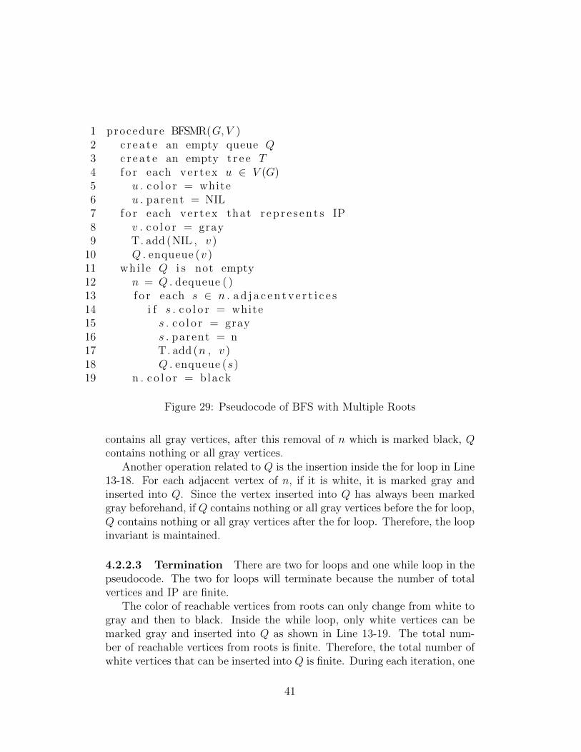
1 procedure BFSMR(G, V )2 c r e a t e an empty queue Q3 c r e a t e an empty t r e e T4 f o r each ver tex u ∈ V (G)5 u . c o l o r = white6 u . parent = NIL7 f o r each ver tex that r e p r e s e n t s IP8 v . c o l o r = gray9 T. add (NIL , v )
10 Q . enqueue (v )11 whi l e Q i s not empty12 n = Q . dequeue ( )13 f o r each s ∈ n . a d j a c e n t v e r t i c e s14 i f s . c o l o r = white15 s . c o l o r = gray16 s . parent = n17 T. add (n , v )18 Q . enqueue (s)19 n . c o l o r = black
Figure 29: Pseudocode of BFS with Multiple Roots
contains all gray vertices, after this removal of n which is marked black, Qcontains nothing or all gray vertices.
Another operation related to Q is the insertion inside the for loop in Line13-18. For each adjacent vertex of n, if it is white, it is marked gray andinserted into Q. Since the vertex inserted into Q has always been markedgray beforehand, if Q contains nothing or all gray vertices before the for loop,Q contains nothing or all gray vertices after the for loop. Therefore, the loopinvariant is maintained.
4.2.2.3 Termination There are two for loops and one while loop in thepseudocode. The two for loops will terminate because the number of totalvertices and IP are finite.
The color of reachable vertices from roots can only change from white togray and then to black. Inside the while loop, only white vertices can bemarked gray and inserted into Q as shown in Line 13-19. The total num-ber of reachable vertices from roots is finite. Therefore, the total number ofwhite vertices that can be inserted into Q is finite. During each iteration, one
41

vertex is removed from Q and marked black. Therefore, after finite numberof iterations, Q will become empty, all vertices will be marked black andBFSMR(G, V ) will terminate.
42
5 Iterative Multiplier
In this chapter, an 8-bit iterative multiplier is implemented to evaluatewhether a QDI system can be reset properly with WRS and start normaloperation without deadlock. The behavior of the iterative multiplier is de-scribed by CHP in the Appendix.
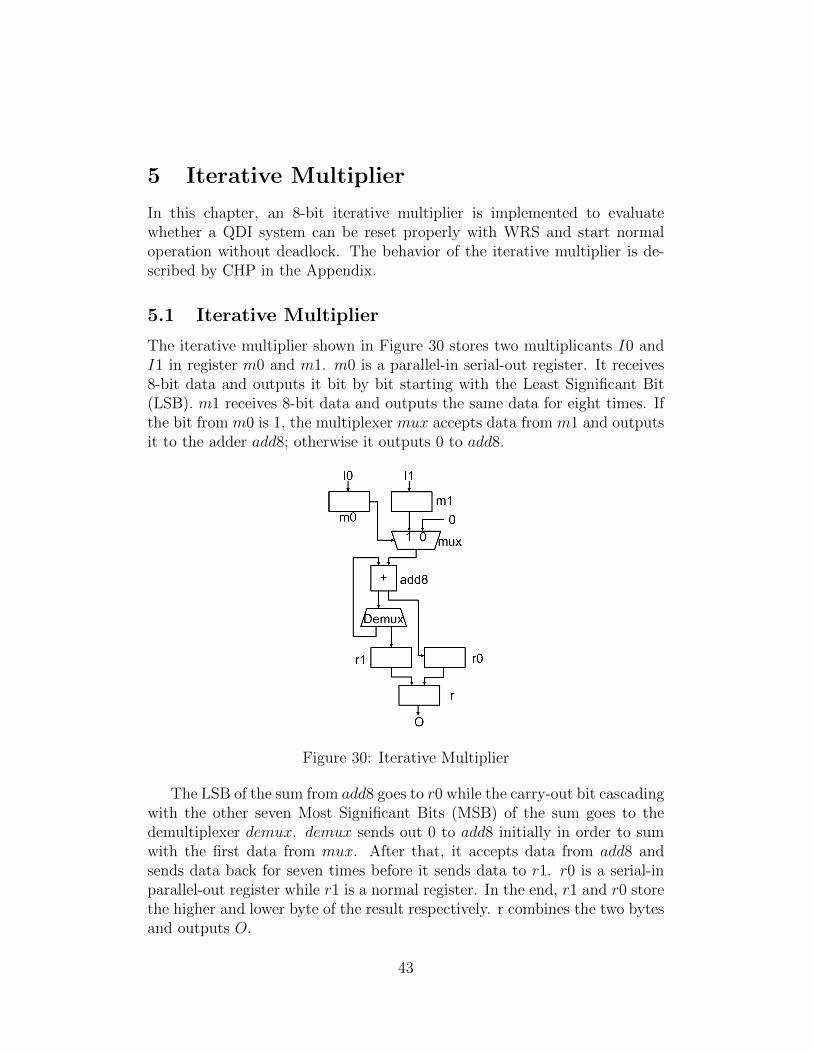
5.1 Iterative Multiplier
The iterative multiplier shown in Figure 30 stores two multiplicants I0 andI1 in register m0 and m1. m0 is a parallel-in serial-out register. It receives8-bit data and outputs it bit by bit starting with the Least Significant Bit(LSB). m1 receives 8-bit data and outputs the same data for eight times. Ifthe bit from m0 is 1, the multiplexer mux accepts data from m1 and outputsit to the adder add8; otherwise it outputs 0 to add8.
Figure 30: Iterative Multiplier
The LSB of the sum from add8 goes to r0 while the carry-out bit cascadingwith the other seven Most Significant Bits (MSB) of the sum goes to thedemultiplexer demux. demux sends out 0 to add8 initially in order to sumwith the first data from mux. After that, it accepts data from add8 andsends data back for seven times before it sends data to r1. r0 is a serial-inparallel-out register while r1 is a normal register. In the end, r1 and r0 storethe higher and lower byte of the result respectively. r combines the two bytesand outputs O.
43
Most of processes in the multiplier are implemented with PCHB tem-plates. The rest are special blocks: Demux is an AP that starts by sending0 to add8. A Source process continues sending 0 to one of the inputs of mux.Some functions such as copy, merge and split are implemented by slack-zeroprocesses.
5.2 Simulation
The multiplier is simulated with an environment that accepts data from O,applies some function to the received data and sends higher and lower bytesof the results to I0 and I1 respectively. Therefore the system is closed andoperates forever.
The multiplier resets and operates correctly under different process tech-nologies, process corners and operating voltages. Reset time is shown inFigure 31. The X-axis specifies different simulation conditions. “LP” refersto TSMC 40nm Low-Power technology while “GS” refers to TSMC 40nmGeneral-Purpose technology. The number following “LP” or “GS” is the op-erating voltage. For example, “06” is 0.6V while “10” is 1V. Three seriesof data represent three different process corners, i.e. TT (Typical NMOS,Typical PMOS), SF (Slow NMOS, Fast PMOS) and FS (Fast NMOS, SlowPMOS).
When the operating voltage increases, the reset time reduces. In addition,at the same voltage, LP process resets slower than GS process as expected.
44
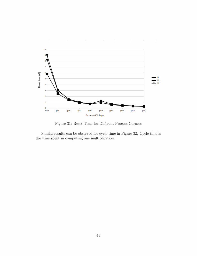
Figure 31: Reset Time for Different Process Corners
Similar results can be observed for cycle time in Figure 32. Cycle time isthe time spent in computing one multiplication.
45
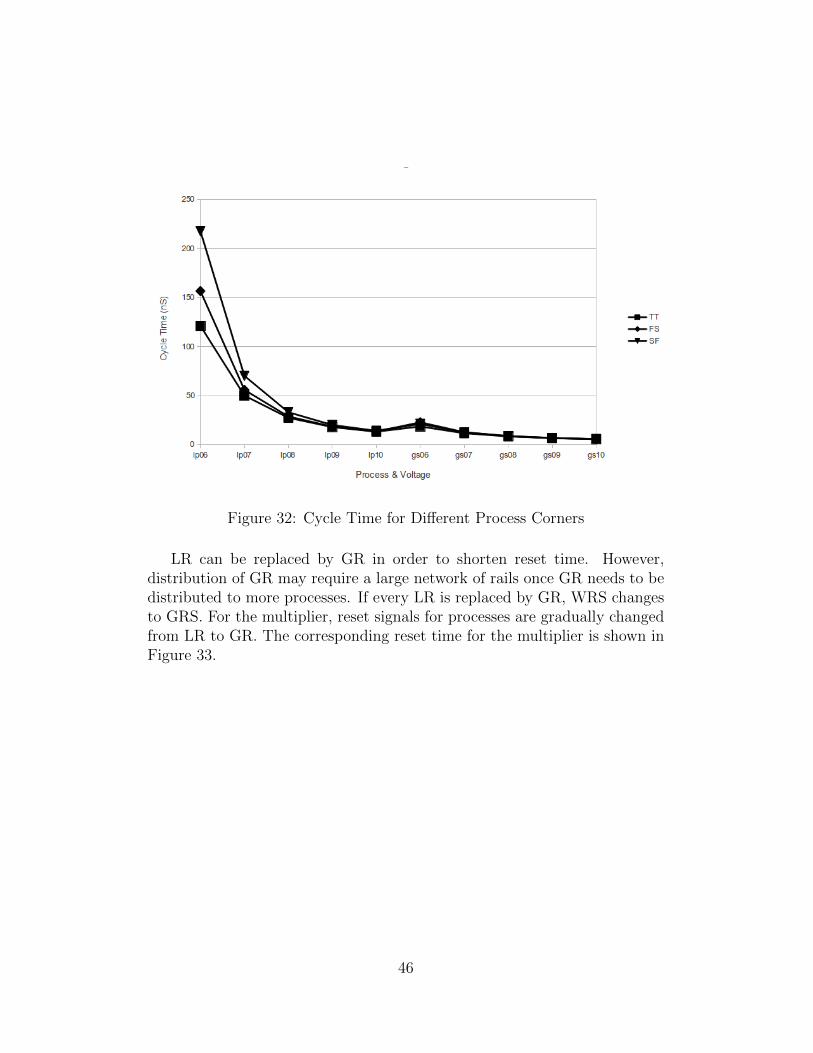
Figure 32: Cycle Time for Different Process Corners
LR can be replaced by GR in order to shorten reset time. However,distribution of GR may require a large network of rails once GR needs to bedistributed to more processes. If every LR is replaced by GR, WRS changesto GRS. For the multiplier, reset signals for processes are gradually changedfrom LR to GR. The corresponding reset time for the multiplier is shown inFigure 33.
46
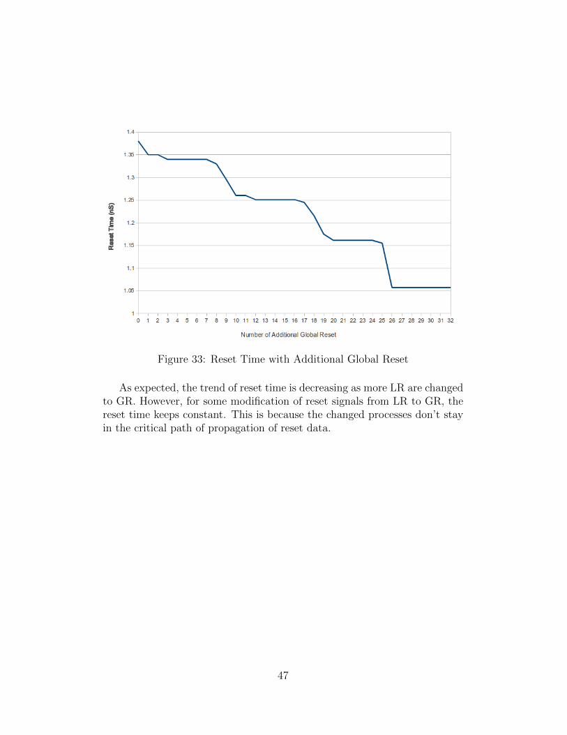
Figure 33: Reset Time with Additional Global Reset
As expected, the trend of reset time is decreasing as more LR are changedto GR. However, for some modification of reset signals from LR to GR, thereset time keeps constant. This is because the changed processes don’t stayin the critical path of propagation of reset data.
47
6 Conclusion
In this thesis, reset schemes for QDI systems have been examined. Circuitimplementation and operation protocol for both GRS and WRS have beendiscussed. Reset time of systems with WRS is dependent on the choiceof LRI. An algorithm has been proposed to systematically choose the LRIin order to shorten the reset time. The proposed WRS has been appliedto an iterative multiplier that operates correctly under different operatingconditions.
In some sense WRS is a more general reset scheme for QDI systems thanGRS. LR in WRS can be changed to GR in order to shorten reset time. Thishas been illustrated by the multiplier application. Once all LR for WRS arechanged to GR, WRS changes to GRS. Therefore, GRS is a special case ofWRS. If there are more LR in the system, the large network of rails andbuffers distributing GR can be removed. All reset signals become local. Onthe other hand, having more GR will reduce the reset time of the QDI system.The choice of the number of GR is application dependent.
Both GRS and WRS rely on reset timing assumption because the stateof the system before reset is “demonic” - all values are possible. We be-lieve it is impossible to implement an asynchronous reset without any timingassumption.
48
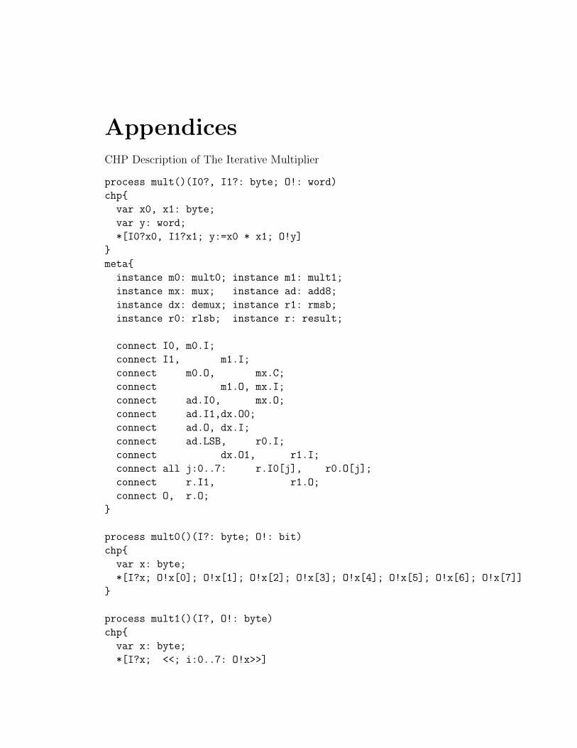
AppendicesCHP Description of The Iterative Multiplier
process mult()(I0?, I1?: byte; O!: word)
chp{
var x0, x1: byte;
var y: word;
*[I0?x0, I1?x1; y:=x0 * x1; O!y]
}
meta{
instance m0: mult0; instance m1: mult1;
instance mx: mux; instance ad: add8;
instance dx: demux; instance r1: rmsb;
instance r0: rlsb; instance r: result;
connect I0, m0.I;
connect I1, m1.I;
connect m0.O, mx.C;
connect m1.O, mx.I;
connect ad.I0, mx.O;
connect ad.I1,dx.O0;
connect ad.O, dx.I;
connect ad.LSB, r0.I;
connect dx.O1, r1.I;
connect all j:0..7: r.I0[j], r0.O[j];
connect r.I1, r1.O;
connect O, r.O;
}
process mult0()(I?: byte; O!: bit)
chp{
var x: byte;
*[I?x; O!x[0]; O!x[1]; O!x[2]; O!x[3]; O!x[4]; O!x[5]; O!x[6]; O!x[7]]
}
process mult1()(I?, O!: byte)
chp{
var x: byte;
*[I?x; <<; i:0..7: O!x>>]
}
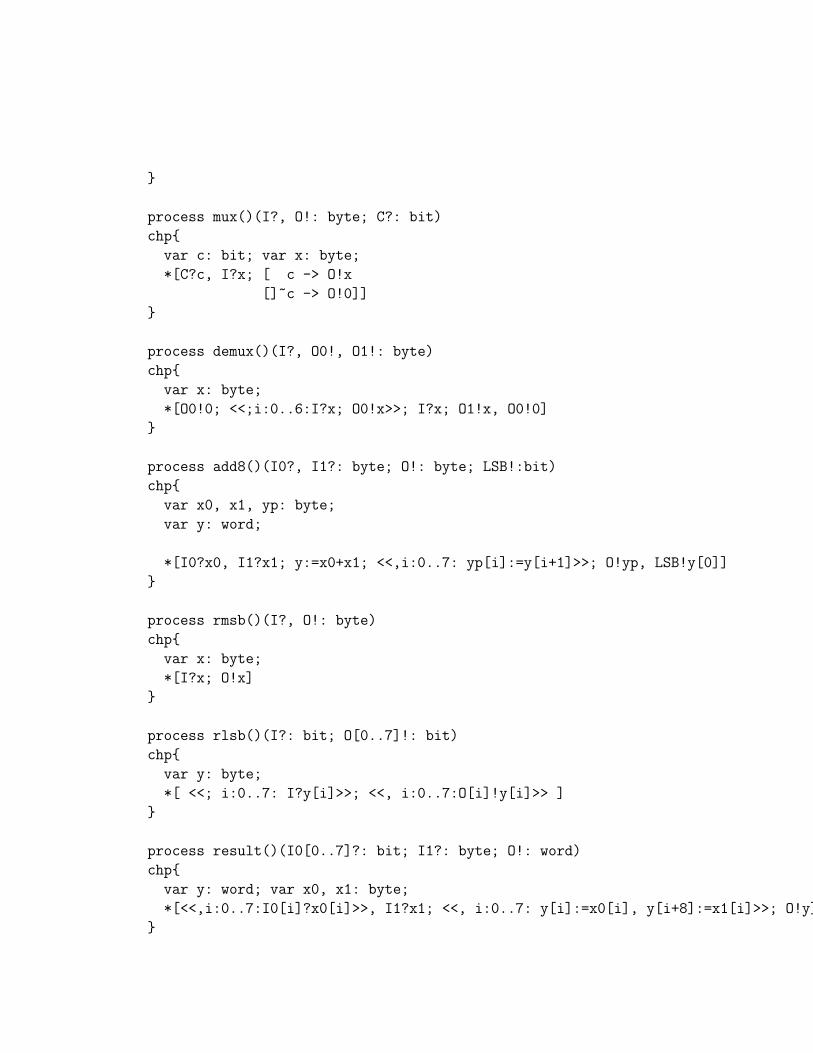
process mux()(I?, O!: byte; C?: bit)
chp{
var c: bit; var x: byte;
*[C?c, I?x; [ c -> O!x
[]~c -> O!0]]
}
process demux()(I?, O0!, O1!: byte)
chp{
var x: byte;
*[O0!0; <<;i:0..6:I?x; O0!x>>; I?x; O1!x, O0!0]
}
process add8()(I0?, I1?: byte; O!: byte; LSB!:bit)
chp{
var x0, x1, yp: byte;
var y: word;
*[I0?x0, I1?x1; y:=x0+x1; <<,i:0..7: yp[i]:=y[i+1]>>; O!yp, LSB!y[0]]
}
process rmsb()(I?, O!: byte)
chp{
var x: byte;
*[I?x; O!x]
}
process rlsb()(I?: bit; O[0..7]!: bit)
chp{
var y: byte;
*[ <<; i:0..7: I?y[i]>>; <<, i:0..7:O[i]!y[i]>> ]
}
process result()(I0[0..7]?: bit; I1?: byte; O!: word)
chp{
var y: word; var x0, x1: byte;
*[<<,i:0..7:I0[i]?x0[i]>>, I1?x1; <<, i:0..7: y[i]:=x0[i], y[i+8]:=x1[i]>>; O!y]
}
References
[1] A. J. Martin and M. Nystrom, “Asynchronous techniques for system-on-chip design” Proc. IEEE Volume 94, Issue 6, pp. 1089-1120, Oct.2006.
[2] A. J. Martin, “The limitation to delay-insensitivity in asynchronous cir-cuits” Sixth MIT Conference on Advanced Research in VLSI, pp. 263-278, 1990.
[3] A. M. Lines “Pipelined Asynchronous Circuits” M.S. thesis, CS, Caltech,Pasadena, CA, 1995
[4] T. H. Cormen, C. E. Leiserson, R. L. Rivest and C. Stein, “Introductionto Algorithms”, 3rd ed. MIT Press and McGraw-Hill 2009, Ch. 22.4, pp.449-451.
[5] P. Prakash, A. J. Martin “Slack Matching Quasi Delay-Insensitive Cir-cuits”, ASYNC 2006, pp. 195-204, 2006.