new process technologies – will silicon cmos carry us to
TRANSCRIPT

MIT Lincoln LaboratoryHPEC 2006 -1CLK 9/19/2006
Craig L. Keast, Chenson Chen, Mike Fritze, Jakub Kedzierski, Dave Shaver
New Process Technologies – Will silicon CMOS carry us to the end of the Roadmap?
HPEC Workshop 2006

MIT Lincoln LaboratoryHPEC 2006 -2CLK 9/19/2006
Outline
• A brief history of CMOS scaling
• Drivers behind “Moore’s Law” and their future outlook
• The potential of “Next Generation” technologies beyond silicon CMOS
• Some comments on 3D circuit integration
• Summary

MIT Lincoln LaboratoryHPEC 2006 -3CLK 9/19/2006
A Few Metrics
• Vacuum tube (early 1900’s) – transistor (1949) –integrated circuit- IC, “chip” (1959)
– During the first 10 years of the chip’s development the US government bought the majority of all ICs produced
– Today the US Government purchases are a few percent of the market
• Today’s microprocessors contain >500 million transistors and occupy ~2-3 cm2 area
– Equivalent number of vacuum tubes would cover an area equal to ~250 football fields
• First ICs cost ~$120 and contained 10 transistors ($12/transistor), today’s microprocessors cost ~$500 and contain 500,000,000 transistors ($0.000001/transistor)
– If this cost scaling was applied to the automobile industry a $100,000 Porsche 911(turbo) would now cost < 1 cent

MIT Lincoln LaboratoryHPEC 2006 -4CLK 9/19/2006
Silicon – The Material Enabling the IC(Semiconductor Wafer Preparation)
Silicon makes up 25.7% of the earth’s crust
Sand
300 mm
Single-Crystal Ingot
Wafer Saw
Silicon’s Oxide (SiO2 ) is a KEY attribute of this material’s success

MIT Lincoln LaboratoryHPEC 2006 -5CLK 9/19/2006
35 Years of CMOS Scalingand Process Improvements
Self-Aligned SilicidesSelf-Aligned Silicides
Presumed Limitto Scaling
Presumed Limitto Scaling
10 μm
1 μm
100 nm
10 nm
1 nm1970 1980 1990 2000 2010 2020
Bulk SiliconSOI ????
CMPCMP
Tech
nolo
gy N
ode
Year
CMOS Replaces BipolarFor High Performance Computing
CMOS Replaces BipolarFor High Performance Computing
CMOS Starts to ReplaceIII-V for Some RF Applications
CMOS Starts to ReplaceIII-V for Some RF Applications
Frontend
Backend
IC cross section
Tungsten PlugsTungsten PlugsHalo ImplantsHalo ImplantsCopper InterconnectCopper Interconnect
Low-k DielectricLow-k DielectricStrained SiliconStrained Silicon
High-k Dielectric???High-k Dielectric???
Self-Aligned GatesSelf-Aligned Gates

MIT Lincoln LaboratoryHPEC 2006 -6CLK 9/19/2006
Drivers Behind Moore’s Law
• Smaller feature sizes– Pack more features in given silicon area
Lower cost per function– Smaller transistors are faster– Smaller transistors and wires consume less energy
• Bigger chips– More functions on one chip reduces packaging and
integration costs, reduces power, improves reliability• Bigger wafer sizes
– More chips per wafer; wafer processing cost for bigger wafers rises more slowly than number of transistors/wafer
• Manufacturing know-how– Faster machines, higher yields, better tool utilization
• More clever device, circuit, and process design– Pack more in a given area, even for a given feature size– “Equivalent scaling”: next generation performance through
improved process/materials: SiGe, SOI, strained silicon

MIT Lincoln LaboratoryHPEC 2006 -7CLK 9/19/2006
Shrinking Feature Size….
Human Hair
~75 μm
0.18 μm180 nmfeature
.
.
~40,000 (65-nm node) transistors could fit on cross-section

MIT Lincoln LaboratoryHPEC 2006 -8CLK 9/19/2006
• Current State of the art (>$25 M)– 65 nm resolution– λ = 193 nm– 0.93 NA (n sinθ)– > 1013 pixels/wafer– ~120 300-mm wafers/hour– Wafer & mask move 100’s of mm/s
during exposure
4x reduction
W ≈ k1λ nsinθ
Lithographic Tools
~10’

MIT Lincoln LaboratoryHPEC 2006 -9CLK 9/19/2006
Optical Lithographic Resolution
• Rayleigh criterion for resolution W
• 30x improvement in resolution over 25 years − λ from 436 nm to 193 nm– sin θ from 0.35 to 0.93– k1 from 0.6 to 0.35– n from 1 to 1
• Now approaching limits− λ limited by materials
and sources– sin θ < 1– k1 > 0.25– n ???
W = k1λ / nsinθ
Slide Courtesy M. Switkes, MIT-LL

MIT Lincoln LaboratoryHPEC 2006 -10CLK 9/19/2006
Liquid Immersion Interference 27-nm Half Pitch
• High-index fluids have been designed and synthesized (n157 = 1.50)• Enable coupling of light from prism to wafer
• No need for solid contact – liquid gap of 2 μm is used
Si mirror
CaF2
Substrate
Spacer Prism
157 nm light
Immersion fluid
sin θ = 0.87
Slide Courtesy M. Rothschild, MIT-LL

MIT Lincoln LaboratoryHPEC 2006 -11CLK 9/19/2006
Optical Lithographyat the Nanometer Level
10 nm gold particle attached to Z-DNA antibody. (John Jackson & Inman. Gene[1989] 84, 221-226)
9-nm polysilicon gate on ultra-thin SOI fabricated at MIT-LL using 248-nm PSM optical lithography (2001)
10 nm
100 nm
9 nm9 nm
100 nm
MIT Lincoln LaboratoryHPEC 2006 -12CLK 9/19/2006
It is likely that we can pattern the smaller feature sizes needed to maintain CMOS scaling….
But will the devices work?

MIT Lincoln LaboratoryHPEC 2006 -13CLK 9/19/2006
Prognosis For Moore’s Law Benefits
Higher Speed? Lower Cost?
Lower Power?
• Historically, CMOS scaling has resulted in simultaneous improvements in cost per function, circuit (and system) speed, power consumption, and packing density
• Will continued scaling give us the same benefits?

MIT Lincoln LaboratoryHPEC 2006 -14CLK 9/19/2006
Lower CostPrognosis For Moore’s Law Benefits
Past• Scaling (s) increases components
per unit area as s2
• Wafer size increase gives more chips per waferIncreasing cost of equipment outweighed by huge increase in number of transistors made per wafer
Future Issues• Skyrocketing equipment costs…Today’s state-of-the-art production facilities
cost ~4 billion dollars• NRE (e.g. >$1M mask sets) and productivity issues favor large volume
production of “generic” components • Increasing consolidation/pooling of fabrication resources and use of
Taiwanese “Super Fabs” TSMC and UMC (China and India next?)How to get DoD-unique and secure components?
0
200
400
600
800
1000
1200
1400
1600
250 180 130 90
Technology Node (nm)
Mas
k Se
t Cos
t (x
$100
0)
Mask Set Cost

MIT Lincoln LaboratoryHPEC 2006 -15CLK 9/19/2006
Lower PowerPrognosis For Moore’s Law Benefits
Past• Supply voltage (V) scales as 1/s• Capacitance (C) scales as 1/s• Energy per op scales as CV2 ∝ 1/ s3
Voltage scaling from 5V to 1V accounted for 25X reduction in power, just by itself
Future Issues• Power supply voltage only projected to
drop 2X over next 15 years (1.0 to 0.5 V)• Subthreshold device operation?
Scaling energy per op is critical to long endurance battery powered systems and to supercomputers (getting power in and heat out)
Passive and Active Power vs Gate Length
E. J. Nowak, IBM J. Res. & Dev., Vol. 46, No. 2/3, p. 173
Stove top
(~1985)

MIT Lincoln LaboratoryHPEC 2006 -16CLK 9/19/2006
Higher SpeedMoore’s Law in Trouble
Processor Speed (INTEL)*
4 GHz
*D. A. Muller, Nature Materials V 4, pg. 645 (2005)
• CPU speed has stalled for the first time in 35 years, with no processor able to break through the “4-Ghz barrier”
• Why?...Gate oxide scaling has stopped at Tox~1.2nm in 2003, at the 90-nm technology node (~3-4 monolayers)
– Only heroic integration efforts, such as use of strained-Si, have made small dents in the CPU speed barrier
– Need a workable High-k gate dielectric in order for performance scaling to continue
Gate Oxide Dielectric*
ResearchProduction
Gate
Channel

MIT Lincoln LaboratoryHPEC 2006 -17CLK 9/19/2006
Future High PerformanceDevice “frontend” Possibilities
• Continue with Si CMOS. Some possible alternative silicon futures are:
– CPU speed could be maxed out –future improvements will come from reduced cost and higher density and integration
– High-k could save the day – if not tomorrow, maybe in 10 years
A perfect high-k gate dielectric will enable CPU speeds to increase until the next tunneling limit (source-to-drain) at the 10nm-node
– Changes in device architecture could take the pressure off the gate oxide, and CPU speed will continue to advance at a slower rate
FDSOI and FinFET lets Tsi scale instead of Tox
Intel - components research (IEDM2003)
With high-k
No high-k

MIT Lincoln LaboratoryHPEC 2006 -18CLK 9/19/2006
Future Possibilities (Cont’d)
• A future with transistors, but without silicon:
– Germanium-based devices Improved mobility, at the expense of many other semiconductor
properties
– Carbon-based devices. Several flavors:
Carbon nanotubes: Have better device properties than Si, but are very difficult to integrate (thus far)
Graphite devices: Difficult to turn off
Molecular devices: Have not been demonstrated to work better than Si

MIT Lincoln LaboratoryHPEC 2006 -19CLK 9/19/2006
Future Possibilities (Cont’d)
• A future without transistors:
– Josephson-junction-based logic Demonstrated and works, but at 4K Real speed and power advantages unclear
– Quantum Computation Can’t execute traditional code, even theoretically But can solve Schrödinger's equation blazingly fast, and factor
very large numbers– Cross Point Arrays – nanowire, molecular
Too simple for general purpose logic, if complexity is increasedto meet logic constraints the result is a transistor
– MEMS, protein, spin logic – too early to evaluate

MIT Lincoln LaboratoryHPEC 2006 -20CLK 9/19/2006
Potential Technology Roadmap
Possible global directions for high performance logic technology in the next 20 years considered in this study,
and graphical summary of their evaluations when possible
Silicon devices
Perfect high-k
Res
earc
h R
equi
red
Estimated Performance
Alternate SiStructuresFDSOIFinFET
Carbon-nanotubedevices
Graphite devices
Germanium devices
Molecular devices
Spintronics – no evaluation possible, insufficient experimental data

MIT Lincoln LaboratoryHPEC 2006 -21CLK 9/19/2006 REF: A. Javey, et al. Nano Lett, 2004.
Future Technology Highlights:Carbon Nanotubes (CNTs)
• Example of experimental CNT device from StanfordFeatures: metal gate, high-k dielectric, metal source/drainHigh performance: 10x Si device of same geometry
• Putting tubes were they are needed is a problem
S
D S
SWNT 100 nm
10-9
10-8
10-7
10-6
10-5
-I DS
(A)
-1.5 -1.0 -0.5 0.0 0.5VG (V)
VDS = -0.1,-0.2,-0.3 VL ~ 50 nm
L~30 nmVDS=-0.3 V10
-8
10-6
-I DS
(A)
-1 0VG (V)
(Drawing and AFM from CEA website)
1 nm

MIT Lincoln LaboratoryHPEC 2006 -22CLK 9/19/2006
Future Technology HighlightsThin Graphite - Graphene
• Graphite has high mobility of >10,000 cm2/Vs (~15x Si)• Graphite is a semi-metal (semiconductor with band-gap of 0eV)
– Difficult to turn off, a fundamental challenge• Proven planar techniques could be used in fabrication
– Planar geometry of devices eliminates majority of integration difficulties of carbon nanotubes
• MIT-LL has begun to explore this material system– Leveraging layer transfer, materials, and microelectronic fabrication
expertise at the Laboratory
REF: K.S Novoselov et al., Science, V. 306, 22 October 2004, p. 666
Few monolayer graphite device SEM and electrical characteristics at T=70K

MIT Lincoln LaboratoryHPEC 2006 -23CLK 9/19/2006 *From 2005 International Technology Roadmap for Semiconductors (ITRS)
LocalInterconnect
GlobalInterconnect
(up to 5)
IntermediateInterconnect
(up to 8)
Cu Metal
Low-κDielectric
Typical Process Cross-Section*
250 180 130 90 65 45 32
Process Technology Node (nm)(year)
Rel
ativ
e D
elay
100
10
1
0.1
Gate Delay(Fan Out 4)
LocalInterconnectGlobalInterconnect(w Repeaters)GlobalInterconnect(w/o Repeaters)
(2004) (2007) (2010) (2013)(2002)(2000)(1998)250 180 130 90 65 45 32
Process Technology Node (nm)(year)
Rel
ativ
e D
elay
100
10
1
0.1
Gate Delay(Fan Out 4)
LocalInterconnectGlobalInterconnect(w Repeaters)GlobalInterconnect(w/o Repeaters)
(2004) (2007) (2010) (2013)(2002)(2000)(1998)ActiveDevice
Relative Wiring Delay vs Feature Size*
The Integrated Circuit Interconnect “backend” Challenge
MIT Lincoln LaboratoryHPEC 2006 -24CLK 9/19/2006
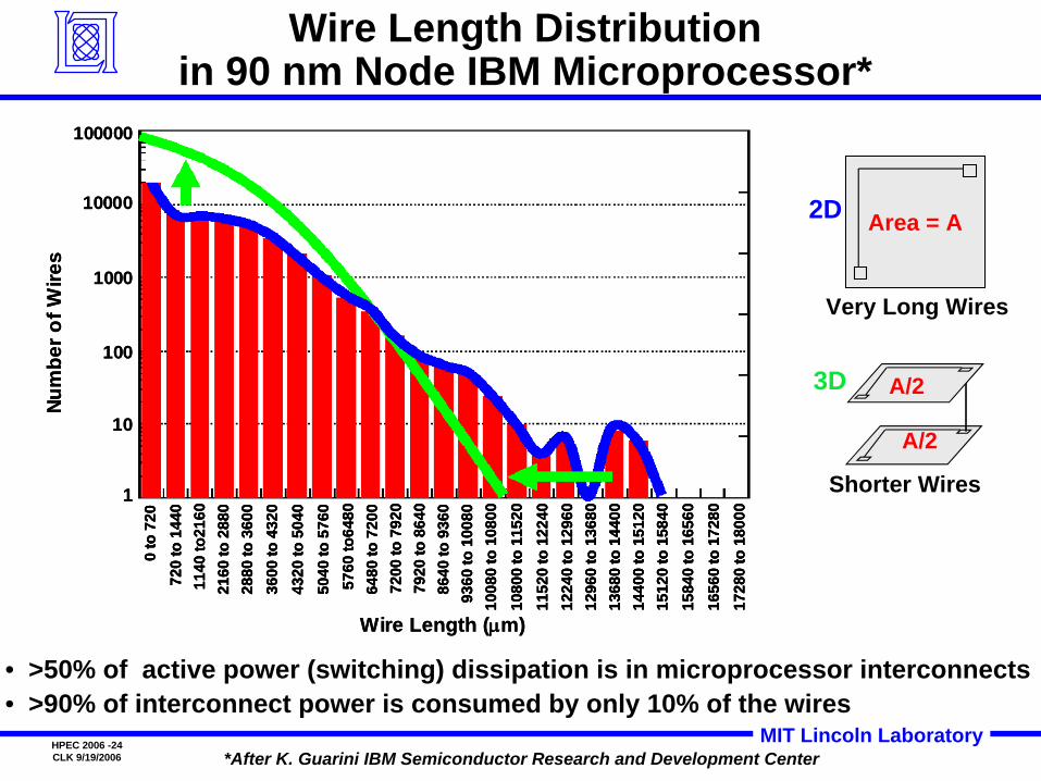
Wire Length Distribution in 90 nm Node IBM Microprocessor*
Area = A
Very Long Wires
Shorter Wires
2D
3D
A/2
A/2
0 to
720
720
to 1
440
1140
to21
6021
60 to
288
028
80 to
360
036
00 to
432
043
20 to
504
050
40 to
576
057
60 to
6480
6480
to 7
200
7200
to 7
920
7920
to 8
640
8640
to 9
360
9360
to 1
0080
1008
0 to
108
0010
800
to 1
1520
1152
0 to
122
4012
240
to 1
2960
1296
0 to
136
8013
680
to 1
4400
1440
0 to
151
2015
120
to 1
5840
1584
0 to
165
6016
560
to 1
7280
1728
0 to
180
00
Wire Length (μm)
Num
ber o
f Wire
s
1
10
100
1000
10000
1000000
to 7
2072
0 to
144
011
40 to
2160
2160
to 2
880
2880
to 3
600
3600
to 4
320
4320
to 5
040
5040
to 5
760
5760
to64
8064
80 to
720
072
00 to
792
079
20 to
864
086
40 to
936
093
60 to
100
8010
080
to 1
0800
1080
0 to
115
2011
520
to 1
2240
1224
0 to
129
6012
960
to 1
3680
1368
0 to
144
0014
400
to 1
5120
1512
0 to
158
4015
840
to 1
6560
1656
0 to
172
8017
280
to 1
8000
0 to
720
720
to 1
440
1140
to21
6021
60 to
288
028
80 to
360
036
00 to
432
043
20 to
504
050
40 to
576
057
60 to
6480
6480
to 7
200
7200
to 7
920
7920
to 8
640
8640
to 9
360
9360
to 1
0080
1008
0 to
108
0010
800
to 1
1520
1152
0 to
122
4012
240
to 1
2960
1296
0 to
136
8013
680
to 1
4400
1440
0 to
151
2015
120
to 1
5840
1584
0 to
165
6016
560
to 1
7280
1728
0 to
180
00
Wire Length (μm)
Num
ber o
f Wire
s
1
10
100
1000
10000
100000
*After K. Guarini IBM Semiconductor Research and Development Center
• >50% of active power (switching) dissipation is in microprocessor interconnects • >90% of interconnect power is consumed by only 10% of the wires

MIT Lincoln LaboratoryHPEC 2006 -25CLK 9/19/2006
Range of Wire in One Clock Cycle*
*After S. Amarasinghe, MIT Laboratory for Computer Science and Artificial Intelligence
0
50
100
150
200
250
300
1995 2000 2005 2010 2015
700 MHz
1.25 GHz
2.1 GHz6 GHz
10 GHz13.5 GHz
Year
(20 mm x 20 mm Die)Proc
ess
Tech
nolo
gy (n
m) From 2003 ITRS Roadmap
• 3D Integration increases accessible active devices

MIT Lincoln LaboratoryHPEC 2006 -26CLK 9/19/2006
Cross-Section of3-Tier 3D-integrated Circuit
3 FDSOI CMOS Transistor Layers, 10-levels of Metal
Tier-1: 180-nm, 1.5V FDSOI CMOS
Tier-2: 180-nm1.5V FDSOI CMOS
Tier-3: 180-nm, 1.5V FDSOI CMOSTier-3: Transistor Layer
Tier-2: Transistor Layer
3D-Via
3-Level Metal
StackedVias
Oxide Bond Interface
Oxide Bond Interface
10 μm
Tier-1: Transistor Layer
3D-Via 3D-Via
Back Metal
Metal Fill

MIT Lincoln LaboratoryHPEC 2006 -27CLK 9/19/2006
Summary
• Transistor feasibility has been demonstrated to below ~10 nm gate lengths
• “Conventional” CMOS (Bulk, SiO2 gate oxide, poly gates) faces significant challenges to scale below 45nm-node
– Ultra-thin-body SOI, FinFET, Dual-Gate, Metal Gate, High-k – No new device technology has yet emerged that is expected to
dethrone silicon CMOS
• Moore’s Law scaling is showing its age and could run into serious speedbumps in the next few years (including economics), but the 2020 roadmap is theoretically feasible
– Process technology improvements are no longer the performance drivers
• Future performance improvements will most likely come through circuit, system architecture, and software advancements