new - issi integrated silicon solution, inc. rev. c 07/20/11 is42s32160c pin configuration package...
TRANSCRIPT

Integrated Silicon Solution, Inc. 1Rev. C07/20/11
Copyright © 2006 Integrated Silicon Solution, Inc. All rights reserved. ISSI reserves the right to make changes to this specification and its products at any time without notice. ISSI assumes no liability arising out of the application or use of any information, products or services described herein. Customers are advised to obtain the lat-est version of this device specification before relying on any published information and before placing orders for products.
IS42S32160C
AUGUST 2011
FEATURES:• Clockfrequency:166,133MHz• Fullysynchronousoperation• Internalpipelinedarchitecture• ProgrammableMode –CAS#Latency:2or3 –BurstLength:1,2,4,8,orfullpage –BurstType:interleavedorlinear• PowersupplyVdd/Vddq +3.3V±0.3V• LVTTLinterface• AutoRefreshandSelfRefresh• IndividualbytecontrolledbyDQM0-3
OPTIONS:• Dierevision:C• Configuration(s):16Mx32• Package(s):90BallBGA(8x13mm)• Lead-freepackageavailable• TemperatureRange:CommercialandIndustrial
16Mx32512Mb SYNCHRONOUS DRAM
DESCRIPTION:TheISSI'sIS42S32160Cisa512MbSynchronousDRAMconfiguredasaquad4Mx32DRAM.Itachieveshigh-speed data transfer using a pipeline architecture with a synchronous interface. All inputs and outputs sig-nals are registered on the rising edge of the clock input, CLK.The512MbSDRAMisinternallyconfiguredbystackingtwo256MB,16Mx16devices.Eachofthe4Mx32banksisorganizedas8192rowsby512columnsby32bits.
KEY TIMING PARAMETERSParameter -6 -75 UnitClk Cycle Time CAS Latency = 2 10 10 ns CASLatency=3 6.0 7.5 nsClkFrequency CASLatency=2 100 100 MHz CASLatency=3 166 133 MHzAccess Time from Clock CASLatency=2 6.5 6.5 ns CASLatency=3 5.4 6 ns
ADDRESS TABLEParameter 16Mx32 Configuration 4Mx32x4banksBankAddressPins BA0,BA1AutoprechargePins A10/APRowAddresses A0–A12ColumnAddresses A0–A8RefreshCount 8192/64ms

2 Integrated Silicon Solution, Inc.Rev. C07/20/11
IS42S32160C
Die 01 Die 02
DQ0 –DQ31
CS
CLK
CKE#
Command
Addresses
CLKCKE
CSRASCASWE
A9A8A7A6A5A4A3A2A1A0
BA0BA1
A10A12
COMMANDDECODER
&CLOCK
GENERATOR MODEREGISTER
REFRESHCONTROLLER
REFRESHCOUNTER
SELF
REFRESH
CONTROLLER
ROWADDRESS
LATCH MU
LTIP
LEX
ER
COLUMNADDRESS LATCH
BURST COUNTER
COLUMNADDRESS BUFFER
COLUMN DECODER
DATA INBUFFER
DATA OUTBUFFER
DQML DQMH
DQ 0-15
VDD/VDDQ
Vss/VssQ
13
13
9
13
13
9
16
16 16
16
512(x 16)
8192
8192
8192
RO
W D
EC
OD
ER 8192
MEMORY CELLARRAY
BANK 0
SENSE AMP I/O GATE
BANK CONTROL LOGIC
ROWADDRESSBUFFER
A11
2
FUNCTIONAL BLOCK DIAGRAM 16Mbx16 SDRAM
FUNCTIONAL BLOCK DIAGRAM 16Mbx32 SDRAM
Integrated Silicon Solution, Inc. — 1-800-379-4774 3Rev. C07/20/11
IS42S32160C
1
PIN DESCRIPTIONS
Symbol Type DescriptionCLK Input Clock:CLK is driven by the system clock.All SDRAM input signals are sampled on the positive edge
of CLK.CLK also increments the internal burst counter and controls the output registers.
CKE Input Clock Enable:CKE activates(HIGH)and deactivates(LOW) the CLK signal.If CKE goes low syn-chronously with clock(set-up and hold time same as other inputs),the internal clock is suspendedfrom the next clock cycle and the state of output and burst address is frozen as long as the CKEremains low.When all banks are in the idle state,deactivating the clock controls the entry to thePower Down and Self Refresh modes.CKE is synchronous except after the device enters PowerDown and Self Refresh modes,where CKE becomes asynchronous until exiting the same mode.The input buffers,including CLK,are disabled during Power Down and Self Refresh modes,providinglow standby power.
BS0,BS1 Input Bank Select:BS0 and BS1 defines to which bank the BankActivate,Read,Write,or BankPrechargecommand is being applied.
A0-A12 Input Address Inputs:A0-A12 are sampled during the BankActivate command (row address A0-A12) andRead/Write command (column address A0-A8 with A10 defining Auto Precharge) to select onelocation in the respective bank.During a Precharge command,A10 is sampled to determine if allbanks are to be precharged (A10 =HIGH).
The address inputs also provide the op-code during a Mode Register Set .
CS# Input Chip Select:CS# enables (sampled LOW) and disables (sampled HIGH) the command decoder.Allcommands are masked when CS# is sampled HIGH.CS#provides for external bank selection onsystems with multiple banks.It is considered part of the command code.
RAS# Input Row Address Strobe:The RAS# signal defines the operation commands in conjunction with theCAS# and WE# signals and is latched at the positive edges of CLK.When RAS# and CS# are as-serted “LOW”and CAS# is asserted “HIGH,”either the BankActivate command or the Prechargecommand is selected by the WE#signal.When the WE#is asserted “HIGH,”the BankActivate com-mand is selected and the bank designated by BS is turned on to the active state.When the WE# isasserted “LOW,”the Precharge command is selected and the bank designated by BS is switched tothe idle state after the precharge operation.
CAS# Input Column Address Strobe:The CAS# signal defines the operation commands in conjunction with theRAS# and WE# signals and is latched at the positive edges of CLK. When RAS# is held “HIGH”andCS#is asserted “LOW,”the column access is started by asserting CAS#”LOW.”Then, the Read orWrite command is selected by asserting WE# “LOW”or “HIGH.”
WE# Input Write Enable:The WE# signal defines the operation commands in conjunction with the RAS# andCAS# signals and is latched at the positive edges of CLK.The WE# input is used to select theBankActivate or Precharge command and Read or Write command.
DQM0-3 Input
Input
Data Input/Output Mask:DQM0-DQM3 are byte specific, nonpersistent I/O buffer controls. The I/Obuffers are placed in a high-z state when DQM is sampled HIGH.Input data is masked when DQMis sampled HIGH during a write cycle.Output data is masked (two-clock latency) when DQM issampled HIGH during a read cycle. DQM3 masks DQ31-DQ24, DQM2 masks DQ23-DQ16, DQM1masks DQ15-DQ8, and DQM0 masks DQ7-DQ0.
DQ0-31 /Output
Data I/O:The DQ0-31 input and output data are synchronized with the positive edge of CLK. The I/Os are byte-maskable during Reads and Writes.

4 Integrated Silicon Solution, Inc.Rev. C07/20/11
IS42S32160C
PIN CONFIGURATION
PACKAGE CODE: B 90 BALL FBGA (Top View) (8.00 mm x 13.00 mm Body, 0.8 mm Ball Pitch)
1 2 3 4 5 6 7 8 9
A
B
C
D
E
F
G
H
J
K
L
M
N
P
R
DQ26
DQ28
VSSQ
VSSQ
VDDQ
VSS
A4
A7
CLK
DQM1
VDDQ
VSSQ
VSSQ
DQ11
DQ13
DQ24
VDDQ
DQ27
DQ29
DQ31
DQM3
A5
A8
CKE
NC
DQ8
DQ10
DQ12
VDDQ
DQ15
VSS
VSSQ
DQ25
DQ30
NC
A3
A6
A12
A9
NC
VSS
DQ9
DQ14
VSSQ
VSS
VDD
VDDQ
DQ22
DQ17
NC
A2
A10
NC
BA0
CAS
VDD
DQ6
DQ1
VDDQ
VDD
DQ23
VSSQ
DQ20
DQ18
DQ16
DQM2
A0
BA1
CS
WE
DQ7
DQ5
DQ3
VSSQ
DQ0
DQ21
DQ19
VDDQ
VDDQ
VSSQ
VDD
A1
A11
RAS
DQM0
VSSQ
VDDQ
VDDQ
DQ4
DQ2
PIN DESCRIPTIONS
A0-A12 Row Address Input
A0-A8 Column Address Input
BA0, BA1 Bank Select Address
DQ0 to DQ31 Data I/O
CLK System Clock Input
CKE Clock Enable
CS Chip Select
RAS Row Address Strobe Command
CAS Column Address Strobe Command
WE Write Enable
DQM0-DQM3 x32 Input/Output Mask
VDD Power
Vss Ground
VDDQ Power Supply for I/O Pin
VssQ Ground for I/O Pin
NC No Connection
Integrated Silicon Solution, Inc. — 1-800-379-4774 5Rev. C07/20/11
IS42S32160C
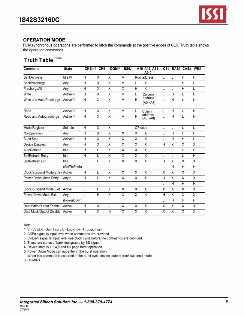
Command State CKEn-1 CKE DQM(6) BS0,1 A10A9-0A12, A11 CS# RAS# CAS# WE#
BankActivate Idle (3) H X X V Row address L L H H
BankPrecharge Any H X X V L X L L H L
PrechargeAll Any H X X X H X L L H L
Write Active (3) H X X V L L H L L
Write and Auto Precharge Active (3) H X X V H L H L L
Read Active (3) H X X V L L H L H
Read and Autoprecharge Active (3) H X X V H L H L H
Mode Register Set Idle H X X OP code L L L L
No-Operation Any H X X X X X L H H H
Burst Stop Active(4) H X X X X X L H H L
Device Deselect Any H X X X X X H X X X
AutoRefresh Idle H H X X X X L L L H
SelfRefresh Entry Idle H L X X X X L L L H
SelfRefresh Exit Idle L H X X X X H X X X
(SelfRefresh) L H H H
Clock Suspend Mode Entry Active H L X X X X X X X X
Power Down Mode Entry Any(5) H L X X X X H X X X
L H H H
Clock Suspend Mode Exit Active L H X X X X X X X X
Power Down Mode Exit Any L H X X X X H X X X
(PowerDown) L H H H
Data Write/Output Enable Active H X L X X X X X X X
Data Mask/Output Disable Active H X H X X X X X X X
Columnaddress(A0 ~A8)
Columnaddress(A0 ~A8)
OPERATION MODEFully synchronous operations are performed to latch the commands at the positive edges of CLK. Truth table showsthe operation commands.
Note:1. V =Valid,X =Don ’t care,L =Logic low,H =Logic high2. CKEn signal is input level when commands are provided. CKEn-1 signal is input level one clock cycle before the commands are provided.3. These are states of bank designated by BS signal.4. Device state is 1,2,4,8,and full page burst operation.5. Power Down Mode can not enter in the burst operation. When this command is asserted in the burst cycle,device state is clock suspend mode.6. DQM0-3
Truth Table (1),(2)

6 Integrated Silicon Solution, Inc.Rev. C07/20/11
IS42S32160C I
®
I
Commands1 BankActivate
(RAS#=”L”, CAS#=”H”, WE#=”H”, BS =Bank, A0-A12 =Row Address)The BankActivate command activates the idle bank designated by the BS0,1 (Bank Select) signal.By latching therow address on A0 to A12 at the time of this command, the selected row access is initiated.The read or writeoperation in the same bank can occur after a time delay of tRCD(min.) from the time of bank activation.Asubsequent BankActivate command to a different row in the same bank can only be issued after the previousactive row has been precharged (refer to the following figure).The minimum time interval between successiveBankActivate commands to the same bank is defined by tRC(min.).The SDRAM has four internal banks on thesame chip and shares part of the internal circuitry to reduce chip area;therefore it restricts the back-to-backactivation of the four banks. tRRD(min.) specifies the minimum time required between activating different banks.After this command is used,the Write command and the Block Write command perform the no mask writeoperation.
CLK
ADDRESS
T0 T1 T2 T3 Tn+3 Tn+4 Tn+5 Tn+6
..............
COMMAND
..............
..............NOP NOP NOP NOP
RAS# - CAS# delay (tRCD) RAS#- RAS# delay time (tRRD)
RAS# Cycle time (tRC)
Bank A Row Addr.
Bank A Col Addr.
Bank BRow Addr.
Bank ARow Addr.
Bank A Activate
R/W A withAutoPrecharge
Bank BActivate
Bank AActivate
Auto PrechargeBegin
:"H" or "L" Bank Activate
2 BankPrecharge command
(RAS#=”L”, CAS#=”H”, WE#=”L”, BS =Bank, A10 =”L”)The BankPrecharge command precharges the bank disignated by BS0,1 signal.Theprecharged bank is switched from the active state to the idle state.This command can be asserted anytime aftertRAS(min.) is satisfied from the BankActivate command in the desired bank.The maximum time any bank can beactive is specified by tRAS(max.).Therefore,the precharge function must be performed in any active bank withintRAS(max.).At the end of precharge, the precharged bank is still in the idle state and is ready to be activated again.

Integrated Silicon Solution, Inc. — 1-800-379-4774 7Rev. C07/20/11
IS42S32160C
3 PrechargeAll command
(RAS#=”L”, CAS#=”H”, WE#=”L”, BS =Don t care, A10 =”H”)The Precharge All command precharges all the four banks simultaneously and can be issued even if all banks arenot in the active state. All banks are then switched to the idle state.
4 Read command
(RAS#=”H”, CAS#=”L”, WE#=”H”, BS =Bank, A10 =”L”, A0-A8 =Column Address)The Read command is used to read a burst of data on consecutive clock cycles from an active row in an activebank.The bank must be active for at least tRCD(min.) before the Read command is issued.During read bursts,the valid data-out element from the starting column address will be available following the CAS# latency after theissue of the Read command.Each subsequent data- out element will be valid by the next positive clock edge (referto the following figure).The DQs go into high-impedance at the end of the burst unless other command is initiated.The burst length,burst sequence,and CAS# latency are determined by the mode register which is alreadyprogrammed. A full-page burst will continue until terminated (at the end of the page it will wrap to column 0 andcontinue).
T0 T2T1 T3 T4 T5 T6 T7 T8
READ A NOP NOP NOP NOP NOP NOP NOP NOP
DOUT A0 DOUT A1 DOUT A2 DOUT A3
DOUT A0 DOUT A1 DOUT A2 DOUT A3
CLK
COMMAND
CAS# latency=2tCK2, DQ- s
CAS# latency=3tCK3, DQ- s
Burst Read Operation(Burst Length =4,CAS#Latency =2,3)
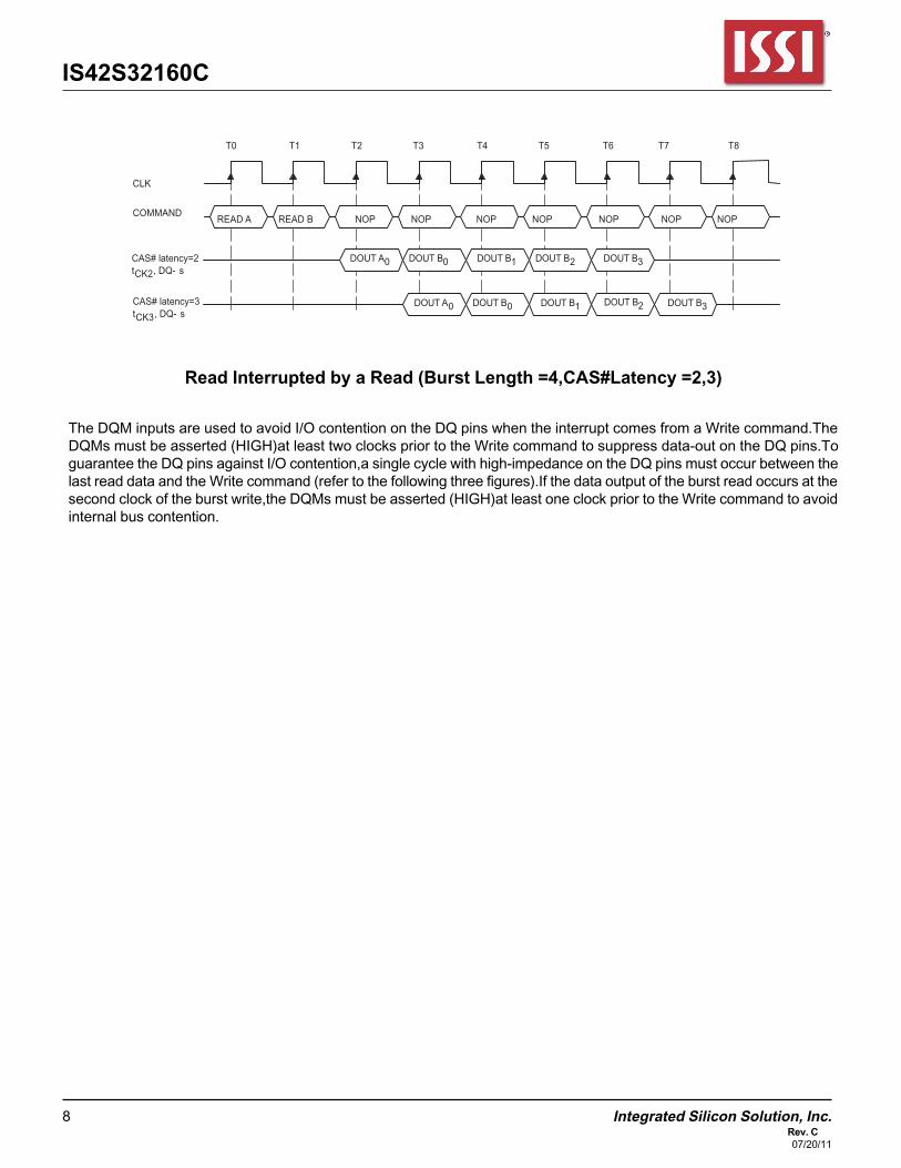
The read data appears on the DQs subject to the values on the DQM inputs two clocks earlier (i.e.DQM latency is two clocksfor output buffers). A read burst without the auto precharge function may be interrupted by a subsequent Read or Writecommand to the same bank or the other active bank before the end of the burst length.It may be interrupted by aBankPrecharge/PrechargeAll command to the same bank too.The interrupt coming from the Read command can occur onany clock cycle following a previous Read command (refer to the following figure).
8 Integrated Silicon Solution, Inc.Rev. C07/20/11
IS42S32160C
READ A READ B NOP NOP NOP NOP NOP NOP NOP
DOUT A0 DOUT B0 DOUT B1 DOUT B2 DOUT B3
DOUT A0 DOUT B0 DOUT B1 DOUT B32DOUT B
CLK
COMMAND
CAS# latency=2tCK2, DQ- s
CAS# latency=3tCK3, DQ- s
T0 T2T1 T3 T4 T5 T6 T7 T8
Read Interrupted by a Read (Burst Length =4,CAS#Latency =2,3)
The DQM inputs are used to avoid I/O contention on the DQ pins when the interrupt comes from a Write command.TheDQMs must be asserted (HIGH)at least two clocks prior to the Write command to suppress data-out on the DQ pins.Toguarantee the DQ pins against I/O contention,a single cycle with high-impedance on the DQ pins must occur between thelast read data and the Write command (refer to the following three figures).If the data output of the burst read occurs at thesecond clock of the burst write,the DQMs must be asserted (HIGH)at least one clock prior to the Write command to avoidinternal bus contention.
Integrated Silicon Solution, Inc. — 1-800-379-4774 9Rev. C07/20/11
IS42S32160C
READ A NOP NOP NOP NOP WRITE B NOP NOP
DQM
COMMAND
DQ’s
NOP
DOUT A DINB2DINB1DINB0
Must be Hi-Z before the Write Command: "H" or "L"
CLK
T0 T2T1 T3 T4 T5 T6 T7 T8
CLK
DQM
COMMAND NOP NOP NOP NOP NOPBANKAACTIVAT E
DIN A 0 DIN A 1 DIN A 2 DIN A 3
1 Clk Interval
CAS# latency=2
READ A WRITEA
: "H" or "L"
NOP
T0 T2T1 T3 T4 T5 T6 T7 T8
tCK2, DQs
CLK
DQM
COMMAND NOP READ A NOP NOP NOP NOP
DIN B0 DIN B1 DIN B2 DIN B3CAS# latency=2
NOP NOP
: "H" or "L"tCK2, DQ’s
T0 T2T1 T3 T4 T5 T6 T7 T8
WRITEB
tCK2, DQs
Read to Write Interval (Burst Length = 4,CAS# Latency =3)
Read to Write Interval (Burst Length = 4,CAS# Latency =2)
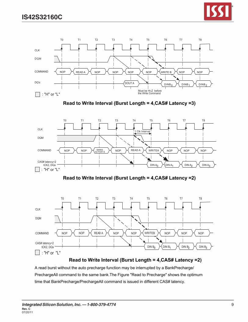
Read to Write Interval (Burst Length = 4,CAS# Latency =2)A read burst without the auto precharge function may be interrupted by a BankPrecharge/
PrechargeAll command to the same bank.The Figure "Read to Precharge" shows the optimum
time that BankPrecharge/PrechargeAll command is issued in different CAS# latency.
10 Integrated Silicon Solution, Inc.Rev. C07/20/11
IS42S32160C I
®
B
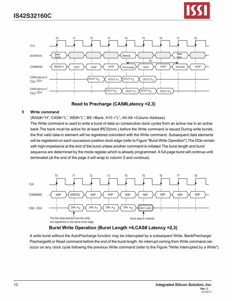
Read to Precharge (CAS#Latency =2,3)5 Write command
(RAS#=”H”, CAS#=”L”, WE#=”L”, BS =Bank, A10 =”L”, A0-A8 =Column Address)The Write command is used to write a burst of data on consecutive clock cycles from an active row in an activebank.The bank must be active for at least tRCD(min.) before the Write command is issued.During write bursts,the first valid data-in element will be registered coincident with the Write command. Subsequent data elementswill be registered on each successive positive clock edge (refer to Figure "Burst Write Operation").The DQs remain with high-impedance at the end of the burst unless another command is initiated.The burst length and burst sequence are determined by the mode register,which is already programmed. A full-page burst will continue until terminated (at the end of the page it will wrap to column 0 and continue).
CLK
COMMAND READ A NOP NOP NOP NOP Activate NOPNOP Precharge
DOUT A0 DOUT A1 DOUT A2 DOUT A3
DOUT A0 DOUT A1 DOUT A2 DOUT A3
ADDRESS
tRP
Bank,Col A Bank(s)
CAS# latency=2tCK2, DQ's
CAS# latency=3tCK3, DQ's
T0 T2T1 T3 T4 T5 T6 T7 T8
Bank,Row
CLK
COMMAND
DIN A 3
NOP WRITEAI NOP NOP NOP NOP NOPNOP NOP
DIN A 0 DIN A 1 DIN A 2DQ0 - DQ3
The first data element and the writeare registered on the same clock edge.
Extra data is masked.
don’t care
T0 T2T1 T3 T4 T5 T6 T7 T8
Burst Write Operation (Burst Length =4,CAS# Latency =2,3)A write burst without the AutoPrecharge function may be interrupted by a subsequent Write, BankPrecharge/PrechargeAll,or Read command before the end of the burst length. An interrupt coming from Write command canoccur on any clock cycle following the previous Write command (refer to the Figure "Write Interrupted by a Write").
Integrated Silicon Solution, Inc. — 1-800-379-4774 11Rev. C07/20/11
IS42S32160C
CLK
COMMAND
DIN B2
NOP WRITEA WRITEB NOP NOP NOP NOP NOPNOP
DIN A0 DIN B0 DIN B1DQ’s DIN B3
1 Clk Interval
T0 T2T1 T3 T4 T5 T6 T7 T8
CLK
COMMAND
T0 T 1 T2 T3 T4 T5 T6 T7 T8
NOP WRITEA NOP NOP NOP NOP NOPREAD B NOP
DIN A0 don’t care DOUT B2DOUT B0 DOUT B1 DOUT B3
DIN A0 don’t care don’t care DOUT B2DOUT B0 DOUT B1 DOUT B3
DI NInput data must be removed from the DQs at least one clockcycle before the Read data appears on the outputs to avoiddata contention.
Input data for the write is masked.
CAS# latency=2tCK2, DQ’s
CAS# latency=3tCK3 , DQ’s
CLK
WRITECOMMAND
BANK (S) ROW
NOP NOPPrecharge NOP NOP Activate
BANKCOL n
DIN DIN n n + 1
DQM
ADDRESS
DQ
tWR
tRP
: don't care
T0 T2T1 T3 T4 T5 T6
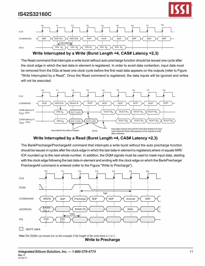
Write Interrupted by a Write (Burst Length =4, CAS# Latency =2,3)The Read command that interrupts a write burst without auto precharge function should be issued one cycle afterthe clock edge in which the last data-in element is registered. In order to avoid data contention, input data mustbe removed from the DQs at least one clock cycle before the first read data appears on the outputs (refer to Figure
"Write Interrupted by a Read". Once the Read command is registered, the data inputs will be ignored and writes will not be executed.
Write Interrupted by a Read (Burst Length =4, CAS# Latency =2,3)The BankPrecharge/PrechargeAll command that interrupts a write burst without the auto precharge functionshould be issued m cycles after the clock edge in which the last data-in element is registered,where m equals tWR/tCK rounded up to the next whole number. In addition, the DQM signals must be used to mask input data, startingwith the clock edge following the last data-in element and ending with the clock edge on which the BankPrecharge/PrechargeAll command is entered (refer to the Figure "Write to Precharge").
Note:The DQMs can remain low in this example if the length of the write burst is 1 or 2.Write to Precharge

10 Integrated Silicon Solution, Inc.Rev. C07/20/11
IS42S32160C I
®
B
Read to Precharge (CAS#Latency =2,3)5 Write command
(RAS#=”H”, CAS#=”L”, WE#=”L”, BS =Bank, A10 =”L”, A0-A8 =Column Address)The Write command is used to write a burst of data on consecutive clock cycles from an active row in an activebank.The bank must be active for at least tRCD(min.) before the Write command is issued.During write bursts,the first valid data-in element will be registered coincident with the Write command. Subsequent data elementswill be registered on each successive positive clock edge (refer to Figure "Burst Write Operation").The DQs remain with high-impedance at the end of the burst unless another command is initiated.The burst length and burst sequence are determined by the mode register,which is already programmed. A full-page burst will continue until terminated (at the end of the page it will wrap to column 0 and continue).
CLK
COMMAND READ A NOP NOP NOP NOP Activate NOPNOP Precharge
DOUT A0 DOUT A1 DOUT A2 DOUT A3
DOUT A0 DOUT A1 DOUT A2 DOUT A3
ADDRESS
tRP
Bank,Col A Bank(s)
CAS# latency=2tCK2, DQ's
CAS# latency=3tCK3, DQ's
T0 T2T1 T3 T4 T5 T6 T7 T8
Bank,Row
CLK
COMMAND
DIN A 3
NOP WRITEAI NOP NOP NOP NOP NOPNOP NOP
DIN A 0 DIN A 1 DIN A 2DQ0 - DQ3
The first data element and the writeare registered on the same clock edge.
Extra data is masked.
don’t care
T0 T2T1 T3 T4 T5 T6 T7 T8
Burst Write Operation (Burst Length =4,CAS# Latency =2,3)A write burst without the AutoPrecharge function may be interrupted by a subsequent Write, BankPrecharge/PrechargeAll,or Read command before the end of the burst length. An interrupt coming from Write command canoccur on any clock cycle following the previous Write command (refer to the Figure "Write Interrupted by a Write").

Integrated Silicon Solution, Inc. — 1-800-379-4774 13Rev. C07/20/11
IS42S32160C I
®
I
(iii) WRITE with Auto Precharge Interrupted by a READ
Interrupted by a READ (with or without auto precharge): A READ to bank m will interrupt a WRITE on bank nwhen registered, with the data-out ap- pearing CAS latency later. The PRECHARGE to bank n will begin aftertWR is met, where tWR begins when the READ to bank m is registered. The last valid WRITE to bank n willbe data-in registered one clock prior to the READ to bank m.
WRITE With Auto Precharge Interrupted by a READ
(iv) WRITE with Auto Precharge Interrupted by a WRITE
Interrupted by a WRITE (with or without auto precharge): A WRITE to bank m will interrupt a WRITE on bank n when when registered. The PRECHARGE to bank n will begin after tWR is met, where tWR begins when the WRITE to bank m is registered. The last valid data WRITE to bank n will be data registered one clock prior to a WRITE to bank m.
WRITE With Auto Precharge Interrupted by a WRITE
DIN
aDIN
d + 2DIN
d + 3
DON’T CARE
T2T1 T4T3 T6T5T0
COMMAND
T7
BANK n
NOP
DIN
d + 1
WRITE - AP BANK n
NOPNOPNOP
NOTE: 1. DQM is LOW.
BANK n,COL a
BANK m,COL d
WRITE - AP BANK m
NOP
DIN
a + 1DIN
a + 2DIN
d
Page Active WRITE with Burst of 4 Write-Back
WR - BANK n tRP - BANK nt WR - BANK m
BANK m
ADDRESS
Internal States
t
Page Active WRITE with Burst of 4 Interrupt Burst, Write-Back Precharge
T2T1 T4T3 T6T5T0
COMMAND WRITE - AP BANK n
NOP NOPNOPNOP
NOTE: 1. DQM is LOW.
BANK n,COL a
BANK m,COL d
READ - AP BANK m
NOPNOP
Page Active READ with Burst of 4
Internal States
t
Page Active WRITE with Burst of 4 Interrupt Burst, Write-Back Precharge
WR - BANK n RP - BANK nt
tRP - BANK m
T7
BANK n
BANK m
ADDRESS
CLK
DQDIN
aDIN
a + 1DOUT
dDOUT
d + 1
CAS Latency = 3 (BANK m)
DON’T CARE
14 Integrated Silicon Solution, Inc.Rev. C07/20/11
IS42S32160C
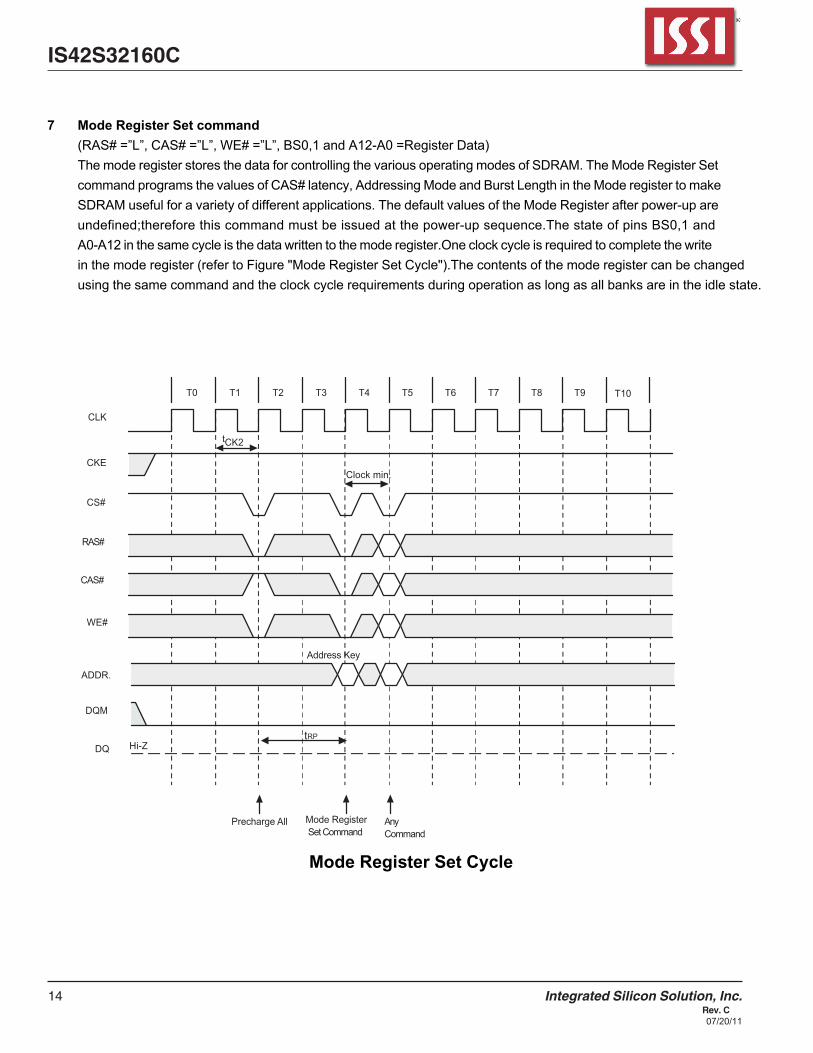
7 Mode Register Set command
(RAS# =”L”, CAS# =”L”, WE# =”L”, BS0,1 and A12-A0 =Register Data)The mode register stores the data for controlling the various operating modes of SDRAM. The Mode Register Setcommand programs the values of CAS# latency, Addressing Mode and Burst Length in the Mode register to makeSDRAM useful for a variety of different applications. The default values of the Mode Register after power-up areundefined;therefore this command must be issued at the power-up sequence.The state of pins BS0,1 andA0-A12 in the same cycle is the data written to the mode register.One clock cycle is required to complete the writein the mode register (refer to Figure "Mode Register Set Cycle").The contents of the mode register can be changed using the same command and the clock cycle requirements during operation as long as all banks are in the idle state.
RAS#
CLK
CKE
CS#
CAS#
WE#
ADDR.
DQM
DQ
tCK2
Clock min.
Address Key
tRPHi-Z
Precharge All Mode RegisterSet Command
AnyCommand
T0 T2T1 T3 T4 T5 T6 T7 T8 T9 T10
Mode Register Set Cycle

Integrated Silicon Solution, Inc. — 1-800-379-4774 15Rev. C07/20/11
IS42S32160C
I
®
I
M
The mode register is divided into various fields depending on functionality.
*Note:RFU (Reserved for future use)should stay 0 during MRS cycle.
Burst Length Field (A2~A0)
This field specifies the data length of column access using the A2~A0 pins and selects the Burst Length to be 2,4, 8, or full page.
A2 A1 A0 Burst Length
0 0 0 10 0 1 20 1 0 40 1 1 81 0 0 Reserved1 0 1 Reserved1 1 0 Reserved1 1 1 Full Page
Address BS0,1 A12-A10 A9 A8 A7 A6 A5 A4 A3 A2 A1 A0
Function RFU* WBL Test Mode CAS Latency BT Burst Length
Data n 0 1 2 3 4 5 6 7 - 255 256 257 -
Column Address n n+1 n+2 n+3 n+4 n+5 n+6 n+7 - n+255 n n+1 -
2 words:
Burst Length 4 words:
8 words:
Full Page: Column address is repeated until terminated.
Burst Type Field (A3)
The Burst Type can be one of two modes,Interleave Mode or Sequential Mode.
• Addressing Sequence of Sequential Mode
An internal column address is performed by increasing the address from the column address which is input to the
device.The internal column address is varied by the Burst Length as shown in the following table. When the value
of column address,(n +m),in the table is larger than 255, only the least significant 8 bits are effective.
A3 Burst Type
0 Sequential
1 Interleave

16 Integrated Silicon Solution, Inc.Rev. C07/20/11
IS42S32160C
• Addressing Sequence of Interleave Mode
A column access is started in the input column address and is performed by inverting the address
bits in the sequence shown in the following table.
CAS# Latency Field (A6~A4)
This field specifies the number of clock cycles from the assertion of the Read command to the first
read data.The minimum whole value of CAS# Latency depends on the frequency of CLK.The
minimum whole value satisfying the following formula must be programmed into this field.
tCAC(min)<=CAS# Latency X tCK
A6 A5 A4 CAS#Latency
0 0 0 Reserved
0 0 1 Reserved
0 1 0 2 clocks
0 1 1 3 clocks
1 X X Reserved
Data n Column Address Burst Length
Data 0 A7 A6 A5 A4 A3 A2 A1 A0
Data 1 A7 A6 A5 A4 A3 A2 A1 A0# 4 words
Data 2 A7 A6 A5 A4 A3 A2 A1# A0
Data 3 A7 A6 A5 A4 A3 A2 A1# A0# 8 words
Data 4 A7 A6 A5 A4 A3 A2# A1 A0
Data 5 A7 A6 A5 A4 A3 A2# A1 A0#
Data 6 A7 A6 A5 A4 A3 A2# A1# A0
Data 7 A7
A8
A8
A8
A8
A8
A8
A8 A8 A6 A5 A4 A3 A2# A1# A0#

Integrated Silicon Solution, Inc. — 1-800-379-4774 17Rev. C07/20/11
IS42S32160C I
®
I
Test Mode field (A8~A7)
These two bits are used to enter the test mode and must be programmed to “00”in normal operation.
Write Burst Length (A9)
This bit is used to select the burst write length.
8 No-Operation command
(RAS# =”H”, CAS# =”H”, WE# =”H”)The No-Operation command is used to perform a NOP to the SDRAM which is selected (CS#
is Low).This prevents unwanted commands from being registered during idle or wait states.9 Burst Stop command
(RAS# =”H”, CAS# =”H”, WE# =”L”)The Burst Stop command is used to terminate either fixed-length or full-page bursts.Thiscommand is only effective in a read/write burst without the auto precharge function.The terminatedread burst ends after a delay equal to the CAS# latency (refer to Figure "Termination of a Burst Read
Operation"). The termination of a write burst is shown in the Figure "Termination of a Burst Write Operation".
Termination of a Burst Read Operation (Burst Length > 4, CAS# Latency =2,3)
Termination of a Burst Write Operation (Burst Length =X)
CLK
COMMAND
T0 T 1 T2 T3 T4 T5 T6 T7 T8
READ A NOP NOP NOP NOP NOP NOPNOP
CAS# latency=2 tCK2,DQ’s
DOUT A0 DOUT A1 DOUT A2 DOUT A3
DOUT A0 DOUT A1 DOUT A2 DOUT A3CAS# latency=3tCK3,DQ’s
The Burst ends after a delay equal to the CAS# latency.
Burst Stop
CLK
COMMAN D
T0 T 1 T2 T3 T4 T5 T6 T7 T8
NOP WRITE A NOP NOP NOP NOP NOPNOP Burst Stop
CAS# latency=2,3 DQ’s DIN A0 DIN A1 DIN A2 don’t care
Input Data for the Write is masked.
A8 A7 Test Mode
0 0 normal mode0 1 Vendor Use Only1 X Vendor Use Only
A9 Write Burst Length
0 Burst1 Single Bit

18 Integrated Silicon Solution, Inc.Rev. C07/20/11
IS42S32160C
10 Device Deselect command (CS# =”H”)
The Device Deselect command disables the command decoder so that the RAS#,CAS#,WE# and Address inputsare ignored,regardless of whether the CLK is enabled.This command is similar to the No Operation command.
11 AutoRefresh command
(RAS# =”L”, CAS# =”L”, WE# =”H”, CKE =”H”)The AutoRefresh command is used during normal operation of the SDRAM and is analogous to CAS#-before-RAS#(CBR)Refresh in conventional DRAMs.This command is non-persistent, so it must be issued each time arefresh is required.The addressing is generated by the internal refresh controller.This makes the address bits a“don’t care”during an AutoRefresh command.The internal refresh counter increments automatically on everyauto refresh cycle to all of the rows.The refresh operation must be performed 8192 times within 64ms. The timerequired to complete the auto refresh operation is specified by tRC(min.).To provide the AutoRefresh command,all banks need to be in the idle state and the device must not be in power down mode (CKE is high in the previous cycle).This command must be followed by NOPs until the auto refresh operation is completed.The prechargetime requirement,tRP(min),must be met before successive auto refresh operations are performed.
12 SelfRefresh Entry command
(RAS# =”L”, CAS# =”L”, WE# =”H”, CKE =”L”)The SelfRefresh is another refresh mode available in the SDRAM. It is the preferred refresh mode for data retentionand low power operation.Once the SelfRefresh command is registered, all the inputs to the SDRAM become “don't
care”with the exception of CKE, which must remain LOW.The refresh addressing and timing is internallygenerated to reduce power consumption.The SDRAM may remain in SelfRefresh mode for an indefinite period.The SelfRefresh mode is exited by restarting the external clock and then asserting HIGH on CKE (SelfRefreshExit command).
13 SelfRefresh Exit command
(CKE =”H”, CS# =”H”or CKE =”H”, RAS# =”H”,CAS# =”H”, WE# =”H”)This command is used to exit from the SelfRefresh mode. Once this command is registered, NOP or Device
Deselect commands must be issued for tRC(min.) because time is required for the completion of any bankcurrently being internally refreshed. If auto refresh cycles in bursts are performed during normal operation, a burstof 8192 auto refresh cycles should be completed just prior to entering and just after exiting the SelfRefresh mode.
14 Clock Suspend Mode Entry /PowerDown Mode Entry command (CKE =”L”)
When the SDRAM is operating the burst cycle, the internal CLK is suspended(masked)from the subsequent cycleby issuing this command (asserting CKE “LOW”). The device operation is held intact while CLK is suspended.Onthe other hand,when all banks are in the idle state,this command performs entry into the PowerDown mode.Allinput and output buffers (except the CKE buffer) are turned off in the PowerDown mode. The device may not remainin the Clock Suspend or PowerDown state longer than the refresh period (64ms) since the command does notperform any refresh operations.
15 Clock Suspend Mode Exit /PowerDown Mode Exit command
When the internal CLK has been suspended, the operation of the internal CLK is initiated from the subsequentcycle by providing this command (asserting CKE “HIGH”). When the device is in the PowerDown mode, the deviceexits this mode and all disabled buffers are turned on to the active state. tPDE(min.) is required when the deviceexits from the PowerDown mode. Any subsequent commands can be issued after one clock cycle from the endof this command.
16 Data Write /Output Enable,Data Mask /Output Disable command (DQM =”L”,”H”)
During a write cycle, the DQM signal functions as a Data Mask and can control every word ofthe input data.During a read cycle, the DQM functions as the controller of output buffers. DQM is also used fordevice selection, byte selection and bus control in a memory system.

Integrated Silicon Solution, Inc. — 1-800-379-4774 19Rev. C07/20/11
IS42S32160C I
®
I
ABSOLUTE MAXIMUM RATINGS(1)
DC RECOMMENDED OPERATING CONDITIONS
Symbol Parameter Min. Typ. Max. UnitVDD Supply Voltage 3.0 3.3 3.6 VVDDQ Supply Voltage for DQ 3.0 3.3 3.6 VVIH High Level Input Voltage (all Inputs) 2.0 — VDD + 0.3 VVIL Low Level Input Voltage (all Inputs) -0.3 — +0.8 V
Notes:1. All voltages are referenced to VSS =0V2. VIH(overshoot): VIH (max) = VDD + 2V (pulse width ≤ 3ns)3. VIL(undershoot): VIL (min) = - 2V (pulse width ≤ 3ns)
CAPACITANCE CHARACTERISTICS(At TA = 0 ~ 70°C, VDD = VDDQ = 3.3 ± 0.3V, VSS = VSSQ = 0V , unless otherwise noted)
Symbol Parameter Min. Max. UnitCIN Input Capacitance, address & control pin 5.0 7.0 pF
CCLK Input Capacitance, CLK pin 5.0 7.6 pFCI/O Data Input/Output Capacitance 8 12 pF
Symbol Parameters Rating Unit
VDD Supply Voltage (with respect to VSS) –0.5 to +4.6 VVDDQ Supply Voltage for Output (with respect to VSSQ) –0.5 to +4.6 VVI Input Voltage (with respect to VSS) –0.5 to VDD+0.5 VVO Output Voltage (with respect to VSSQ) –1.0 to VDDQ+0.5 VICS Short circuit output current 50 mAPD Power Dissipation (TA = 25 °C) 1 WTOPT Operating Temperature Com. 0 to +70 °C
Ind. -40 to +85
TSTG Storage Temperature –55 to +150 °C
Notes:1. Exposing the device to stress above those listed in Absolute Maximum Ratings could cause permanent damage. The device is not meant
to be operated under conditions outside the limits described in the operational section of this specification. Exposure to AbsoluteMaximum Rating conditions for extended periods may affect device reliability.

20 Integrated Silicon Solution, Inc.Rev. C07/20/11
IS42S32160C
Symbol Unit Note
Operating CurrenttRC ≥ tRC(min), Outputs Open, Inputsignal one transition per one cycle
1 bankoperation
IDD1 3
Precharge Standby Current in power down mode
Precharge Standby Current in non-power down mode
Precharge Standby Current in non-power down mode
tCK = 15ns, CKE ≤ VIL(max)IDD2P
IDD2N
IDD2NS
Precharge Standby Current in power down mode tCK = ∞, CKE ≤ VIL(max)
IDD2PS
-75-6Max.
270300
4
4
4
4
60
40 40
60
Parameter Description Min. Max. Unit Note
IIL Input Leakage Current(0V ≤ VIN ≤ VDD, All other pins not under test = 0V )
- 5 + 5 µA
IOL
2.4 VVOHLVTTL Output "H" Level Voltage
( IOUT = -2mA )
VOLLVTTL Output "L" Level Voltage
( IOUT = 2mA )0.4 V
Output Leakage Current(0V ≤ VOUT ≤ VDD, DQ disable )
- 5 + 5 µA
D.C. ELECTRICAL CHARACTERISTICS (RECOMMENDED OPERATING CONDITIONS)
CKE VIH(min), CS# ≥ VIH(min), tCK = 15ns
CKE ≥ VIH(min), CLK ≤ VIL(max), tCK = ∞ Active Standby Current in power down mode CKE ≤ VIL(max), tCK = 15ns
IDD3P
Active Standby Current in power down mode CKE& CLK ≤ VIL(max), tCK = ∞
IDD3PS
Active Standby Current in non-power down mode CKE VIH(min), CS# ≥ VIH(min), tCK = 15ns
IDD3N
Active Standby Current in non-power down mode CKE ≥
≥
VIH(min), CLK ≤ VIL(max), tCK = ∞ IDD3NS
Operating Current (Burst mode)tCK =tCK(min), Outputs Open, Multi-bank interleave
IDD4 3, 4
Refresh Current tRC ≥ tRC(min)
IDD5 3
Self Refresh Current CKE ≤ 0.2V
IDD61
6
6
80
50
260
320
6
6
6
80
50
300
360
6
mA
Description/ Test Condition
Integrated Silicon Solution, Inc. — 1-800-379-4774 21Rev. C07/20/11
IS42S32160C
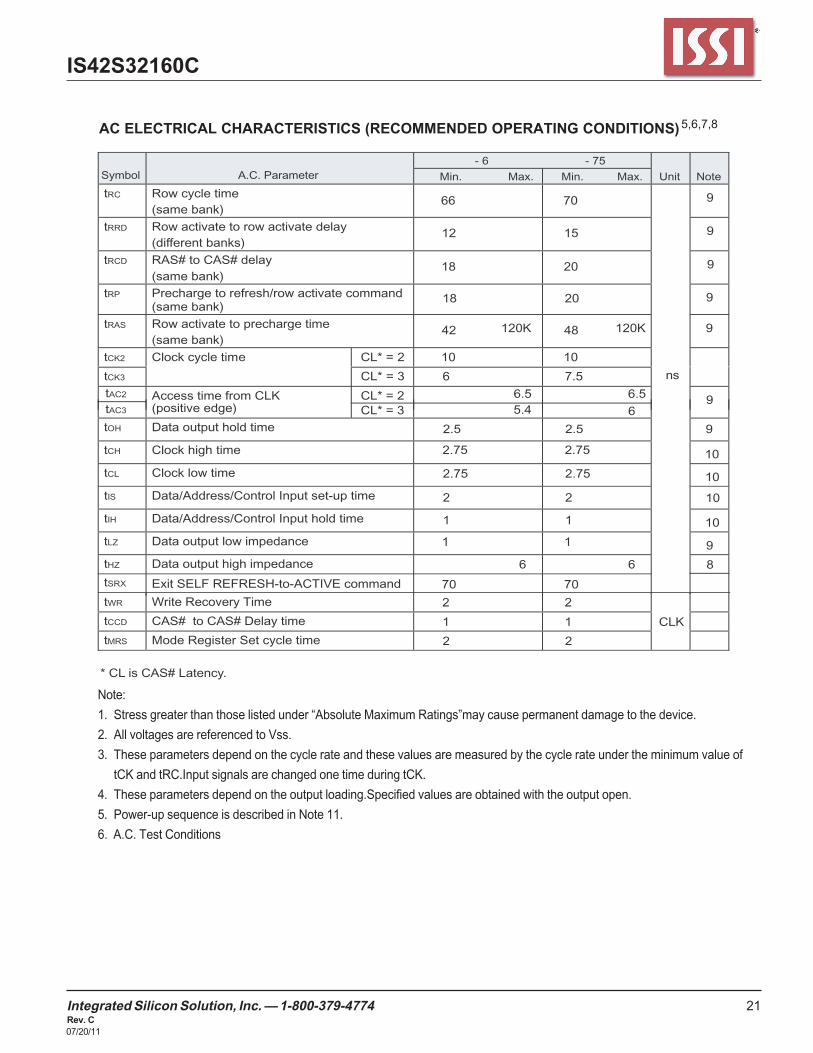
- 75- 6Symbol A.C. Parameter Min. Max.Max. Min. Unit Note
tRC Row cycle time (same bank)
9
tRRD Row activate to row activate delay(different banks)
9
tRCD RAS# to CAS# delay (same bank)
9
tRP Precharge to refresh/row activate command(same bank)
9
tRAS Row activate to precharge time(same bank)
9
tCK2 Clock cycle time CL* =
CL* = 2CL* = 3
2
tCK3 CL* = 3 ns
Access time from CLK 9tAC2
tAC3 (positive edge)
tOH Data output hold time 9 9
tCH Clock high time 10
tCL Clock low time 10
tIS Data/Address/Control Input set-up time 10
tIH Data/Address/Control Input hold time 10
tLZ Data output low impedance 9
tHZ
tSRX
Data output high impedance
Exit SELF REFRESH-to-ACTIVE command
120K120K
65.46.5 6.5
8 8
70
15
20
20
48
10
7.5
2.5
2.75
2.75
2
1
1
66
12
18
18
42
10
6
2.5
2.75
2.75
2
1
1
6
70 70
6
tWR Write Recovery Time
tCCD CAS# to CAS# Delay time CLK
tMRS Mode Register Set cycle time
2
1
2
2
1
2
E
AC ELECTRICAL CHARACTERISTICS (RECOMMENDED OPERATING CONDITIONS)5,6,7,8
* CL is CAS# Latency.
Note:
1. Stress greater than those listed under “Absolute Maximum Ratings”may cause permanent damage to the device.
2. All voltages are referenced to Vss.
3. These parameters depend on the cycle rate and these values are measured by the cycle rate under the minimum value of
tCK and tRC.Input signals are changed one time during tCK.
4. These parameters depend on the output loading.Specified values are obtained with the output open.
5. Power-up sequence is described in Note 11.
6. A.C. Test Conditions

22 Integrated Silicon Solution, Inc.Rev. C07/20/11
IS42S32160C
Reference Level of Output Signals 1.4V /1.4V
Output Load Reference to the Under Output Load
Input Signal Levels 2.4V /0.4V
Transition Time (Rise and Fall)of Input Signals 1ns
Reference Level of Input Signals 1.4V
1.4V
50Ω
Output
30pF
Z0=50Ω
LVTTL A.C. Test Load
7. Transition times are measured between VIH and VIL.Transition(rise and fall) of input signals are in a fixed slope
(1 ns).
8. tHZ defines the time in which the outputs achieve the open circuit condition and are not at reference levels.
9. If clock rising time is longer than 1 ns, (tR /2 -0.5)ns should be added to the parameter.
10. Assumed input rise and fall time tT (tR &tF )= 1 ns
If tR or tF is longer than 1 ns,transient time compensation should be considered,i.e.,[(tr +tf)/2 -1 ]ns
should be added to the parameter.
11. Power up Sequence
Power up must be performed in the following sequence.
(i) Power must be applied to VDD and VDDQ (simultaneously) when all input signals are held “NOP”state
and both CKE =”H”and DQM =”H.”The CLK signals must be started at the same time
(ii) After power-up,a pause of 200µ seconds minimum is required.Then,it is recommended that DQM is
held “HIGH”(VDD levels)to ensure DQ output is in high impedence.
(iii) All banks must be precharged.
(iv) Mode Register Set command must be asserted to initialize the Mode register.
(v) A minimum of 2 Auto-Refresh dummy cycles must be required to stabilize the internal circuitry of the device.
LVTTL Interface
Integrated Silicon Solution, Inc. — 1-800-379-4774 23Rev. C07/20/11
IS42S32160C I
®
I
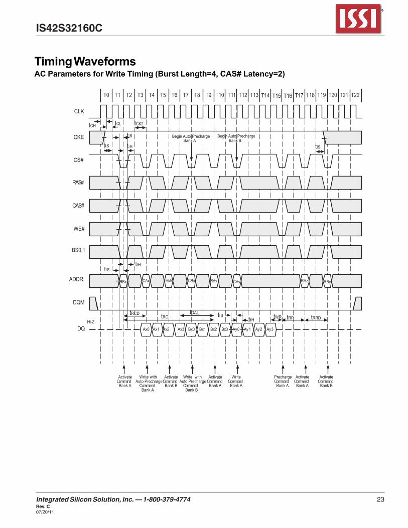
Timing WaveformsAC Parameters for Write Timing (Burst Length=4, CAS# Latency=2)
-5 , , -7 , x x
BS0,1
tCH tCL tCK2
tIStIS tIH
Begin Auto PrechargeBank A
Begin Auto PrechargeBank B
tIS
tIHtIS
RBx CAx RBx CBx RAy CAy RAz RBy
tRCD tDALtRC tIStIH tWR tRP tRRD
Ax0 Ax1 Ax2 Ax3 Bx0 Bx1 Bx2 Bx3 Ay0 Ay1 Ay2 Ay3
ActivateCommand
Bank A
Write withAuto Precharge
CommandBank A
ActivateCommand
Bank B
Write withAuto Precharge
CommandBank B
ActivateCommand
Bank A
WriteCommand
Bank A
PrechargeCommand
Bank A
ActivateCommand
Bank A
ActivateCommand
Bank B
CLK
CKE
CS#
RAS#
CAS#
WE#
ADDR.
DQM
DQHi-Z
T0 T2T1 T3 T4 T5 T6 T7 T9T8 T12T11T10 T14T13 T15 T16 T17 T18 T19 T21T20 T22

24 Integrated Silicon Solution, Inc.Rev. C07/20/11
IS42S32160C
AC Parameters for Read Timing (Burst Length=2, CAS# Latency=2)
A10
ADD
DQ
tCH tCL tCK2
tIS
tIS
tIH
Begin AutoPrechargeBank B
tIH
tIH
tIS
RAx
RAx CAx RBx
RBx
CBx
RAy
RAy
tRRDtRAS
tRC
tRCDtAC2tLZ
tOH
tHZ
Ax0 Ax1 Bx0 Bx1
tRP
ActivateCommandBank A
ReadCommand
Bank A
ActivateCommand
Bank B
Read withAuto Precharge
CommandBank B
PrechargeCommandBank A
ActivateCommand
Bank A
Hi-ZtAC2
tHZ
T0 T2T1 T3 T4 T5 T6 T7 T9T8 T12T11T10 T13
BS0,1
CLK
CKE
CS#
RAS#
CAS#
WE#
DQM

Integrated Silicon Solution, Inc. — 1-800-379-4774 25Rev. C07/20/11
IS42S32160C
A10
ADD
DQM
DQ
tCK2
RAx
RAx CAx
tRPtRC
Ax0 Ax1 Ax2 Ax3
Precharge AllCommand
Auto RefreshCommand
Auto RefreshCommand
ActivateCommand
Bank A
ReadCommand
Bank A
tRC
T0 T2T1 T3 T4 T5 T6 T7 T9T8 T12T11T10 T14T13 T15 T16 T17 T18 T19 T21T20 T22
BS0,1
CLK
CKE
CS#
RAS#
CAS#
WE#
DQ
Auto Refresh (CBR)(Burst Length=4, CAS# Latency=2)

26 Integrated Silicon Solution, Inc.Rev. C07/20/11
IS42S32160C
Power on Sequence and Auto Refresh (CBR)
T0 T1 T2 T3 T4 T5 T6 T7 T8 T9 T10 T11 T12 T13 T14 T15 T16 T17 T18 T19 T20 T21 T22
CLK
CKE
CS
RAS
CAS
WE
A10
ADD
DQM
DQ
High levelis required Minimum of 2 Refresh Cycles are required
tMRS
tRP
High Level is Necessary
tRC
Address Key
Inputs
be stable for 200us
Precharge
All Banksmust Command
1st Auto
CommandRefresh
2nd Auto RefreshCommand
Mode Set Command
CommandRegister
Hi-Z
BS0, 1

Integrated Silicon Solution, Inc. — 1-800-379-4774 27Rev. C07/20/11
IS42S32160C I
®
I
Self Refresh Entry & Exit Cycle
Note:To Enter SelfRefresh Mode1. CS#,RAS#&CAS#with CKE should be low at the same clock cycle.2. After 1 clock cycle,all the inputs including the system clock can be don ’t care except for CKE.3. The device remains in SelfRefresh mode as long as CKE stays “low”.
Once the device enters SelfRefresh mode,minimum tRAS is required before exit from SelfRefresh.To Exit SelfRefresh Mode1. System clock restart and be stable before returning CKE high.2. Enable CKE and CKE should be set high for minimum time of tSRX.3. CS#starts from high.4. Minimum tRC is required after CKE going high to complete SelfRefresh exit.5. 8192 cycles of burst AutoRefresh is required before SelfRefresh entry and after SelfRefresh exit if the system uses burst refresh.
CLK
CKE
CS#
RAS#
CAS#
BS0,1
ADD
WE#
DQM
DQ
*Note 1
*Note 2
tIS
*Note 3
*Note 4 tRC(min) *Note 7
*Note 5
*Note 6
*Note 8
*Note 8
Hi-Z Hi-Z
SelfRefresh Enter SelfRefresh Exit Auto Refresh
tSRX
tPDE
T0 T2T1 T3 T4 T5 T6 T7 T9T8 T12T11T10 T14T13 T15 T16 T17 T18 T19
28 Integrated Silicon Solution, Inc.Rev. C07/20/11
IS42S32160C
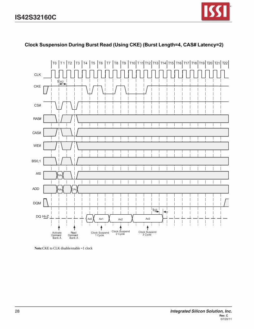
Clock Suspension During Burst Read (Using CKE) (Burst Length=4, CAS# Latency=2)
T0 T 1 T2 T3 T4 T5 T6 T7 T8 T9 T10 T 11 T12 T13 T14 T15 T16 T17 T18 T19 T20 T21 T22
tCK2
RAx
RAx CAx
Hi-ZAx0 Ax1 Ax2 Ax3
ActivateCommand
Bank A
ReadCommand
Bank A
Clock Suspend1 Cycle
tHZ
CLK
CKE
CS#
RAS#
CAS#
WE#
BS0,1
A10
ADD
DQM
DQ
Clock Suspend2 Cycle
Clock Suspend3 Cycle
Note:CKE to CLK disable/enable =1 clock

Integrated Silicon Solution, Inc. — 1-800-379-4774 29Rev. C07/22/11
IS42S32160C I
®
I
Clock Suspension During Burst Read (Using CKE) (Burst Length=4, CAS# Latency=3)
(
Note:CKE to CLK disable/enable =1 clock
T0 T 1 T3 T4 T5 T6 T7 T8 T9 T10 T 11 T12 T13 T14 T15 T16 T17 T18 T19 T20 T21 T22
tCK3
RAx
RAx CAx
Hi-ZAx0 Ax1 Ax2 Ax3
tHZ
T 2
Clock Suspend1 Cycle
Clock Suspend2 Cycle
Clock Suspend3 Cycle
ActivateCommand
Bank A
ReadCommand
Bank A
CLK
CKE
CS#
RAS#
CAS#
WE#
BS0,1
A10
ADD
DQM
DQ Hi-Z

30 Integrated Silicon Solution, Inc.Rev. C07/20/11
IS42S32160C
T0 T 1 T2 T3 T4 T5 T6 T7 T8 T9 T10 T 11 T12 T13 T14 T15 T16 T17 T18 T19 T20 T21 T22
tCK2
RAx
RAx CAx
DAx0 DAx1 DAx2 DAx3
CLK
CKE
CS#
RAS#
CAS#
WE#
BS0,1
A10
ADD
DQM
DQ Hi-Z
ActivateCommandBank A
WriteCommandBank A
Clock Suspend1 Cycle
Clock Suspend2 Cycle
Clock Suspend3 Cycle
Clock Suspension During Burst Write (Using CKE) (Burst Length=4, CAS# Latency=2)
(
Note:CKE to CLK disable/enable =1 clock

Integrated Silicon Solution, Inc. — 1-800-379-4774 31Rev. C07/20/11
IS42S32160C
I
®
I
Clock Suspension During Burst Write (Using CKE) (Burst Length=4, CAS# Latency=3)
(
Note:CKE to CLK disable/enable =1 clock
T0 T 1 T2 T3 T4 T5 T6 T7 T8 T9 T10 T 11 T12 T13 T14 T15 T16 T17 T18 T19 T20 T21 T22
DAx0 DAx1 DAx2 DAx3
tCK3
RAx
RAx CAx
CLK
CKE
CS#
RAS#
CAS#
WE#
BS0,1
A10
ADD
DQM
DQ Hi-Z
ActivateCommandBank A
Clock Suspend1 Cycle
Clock Suspend2 Cycle
Clock Suspend3 Cycle
WriteCommandBank A

32 Integrated Silicon Solution, Inc.Rev. C07/20/11
IS42S32160C
T0 T 1 T2 T3 T4 T5 T6 T7 T8 T9 T10 T 11 T12 T13 T14 T15 T16 T17 T18 T19 T20 T21 T22
tCK2 tIS tPDE
RAx
RAx CAx
tHZ
Ax3Ax2Ax1Ax0
Power DownMode Entry
Power DownMode Entry
Mode Exit
Clock MaskStart
STANDBY
Any
Valid
ACTIVESTANDBY
CLK
CKE
CS#
RAS#
CAS#
WE#
BS0,1
A10
ADD
DQM
DQHi-Z
ActivateCommandBank A
ReadCommandBank A
Power Down
Mode ExitPower DownClock Mask
EndPrechargeCommandBank A
PRECHARGE
Command
Power Down Mode and Clock Mask (Burst Length=4, CAS# Latency=2)

Integrated Silicon Solution, Inc. — 1-800-379-4774 33Rev. C07/20/11
IS42S32160C
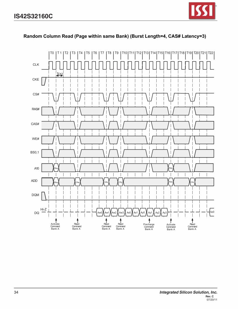
Random Column Read (Page within same Bank) (Burst Length=4, CAS# Latency=2)
T0 T 1 T2 T3 T4 T5 T6 T7 T8 T9 T10 T 11 T12 T13 T14 T15 T16 T17 T18 T19 T20 T21 T22
tCK2
Aw0 Aw1 Aw2 Aw3 Ax0 Ax1 Ay0 Ay1 Ay2 Ay3
RAw
RAw CAw CAx CAy CAz
Az0 Az1 Az2 Az3
Activate
RAz
RAz
CLK
CKE
CS#
RAS#
CAS#
WE#
BA0,1
A10
ADD
DQM
DQ Hi-Z
ActivateCommandBank A
ReadCommandBank A
PrechargeCommandBank A
ReadCommandBank A
CommandBank A
ReadCommandBank A
ReadCommandBank A
34 Integrated Silicon Solution, Inc.Rev. C07/20/11
IS42S32160C
Random Column Read (Page within same Bank) (Burst Length=4, CAS# Latency=3)
T0 T 1 T2 T3 T4 T5 T6 T7 T8 T9 T10 T 11 T12 T13 T14 T15 T16 T17 T18 T19 T20 T21 T22
tCK3
Aw0 Aw1 Aw2 Aw3 Ax0 Ax1 Ay0 Ay1 Ay2 Ay3
RAw
RAw CAw CAx CAy CAz
RAz
RAz
Az0
CLK
CKE
CS#
RAS#
CAS#
WE#
BS0,1
A10
ADD
DQM
DQHi-Z
ActivateCommandBank A
ActivateCommandBank A
ReadCommandBank A
ReadCommandBank A
ReadCommandBank A
ReadCommandBank A
PrechargeCommandBank A

Integrated Silicon Solution, Inc. — 1-800-379-4774 35Rev. C07/20/11
IS42S32160C
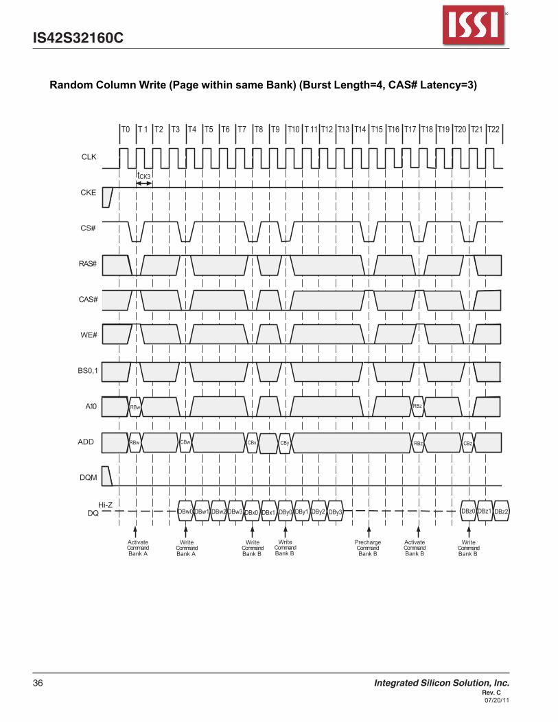
Random Column Write (Page within same Bank) (Burst Length=4, CAS# Latency=2)
T0 T 1 T2 T3 T4 T5 T6 T7 T8 T9 T10 T 11 T12 T13 T14 T15 T16 T17 T18 T19 T20 T21 T22
tCK2
DBw0 DBx0 DBx1 DBy0
RBw
CBw CBx CBy CBz
RBz
RBzRBw
DBw1 DBw2 DBw3 DBy1 DBy2 DBy3 DBz0 DBz1 DBz2 DBz3
CLK
CKE
CS#
RAS#
CAS#
WE#
BS0,1
A10
ADD
DQM
DQHi-Z
WriteCommandBank A
WriteCommandBank B
WriteCommandBank B
WriteCommandBank B
ActivateCommandBank A
ActivateCommandBank B
PrechargeCommandBank B
36 Integrated Silicon Solution, Inc.Rev. C07/20/11
IS42S32160C
Random Column Write (Page within same Bank) (Burst Length=4, CAS# Latency=3)
T0 T 1 T2 T3 T4 T5 T6 T7 T8 T9 T10 T 11 T12 T13 T14 T15 T16 T17 T18 T19 T20 T21 T22
tCK3
DBw0 DBx0 DBx1
RBw CBw CBx CBy CBz
DBz0
RBz
RBz
RBw
DBz1 DBz2DBw1 DBw2 DBw3 DBy0 DBy1 DBy2 DBy3
CLK
CKE
CS#
RAS#
CAS#
WE#
BS0,1
A10
ADD
DQM
DQHi-Z
WriteCommandBank A
WriteCommandBank B
WriteCommandBank B
WriteCommandBank B
ActivateCommandBank A
ActivateCommandBank B
PrechargeCommandBank B
Integrated Silicon Solution, Inc. — 1-800-379-4774 37Rev. C07/20/11
IS42S32160C
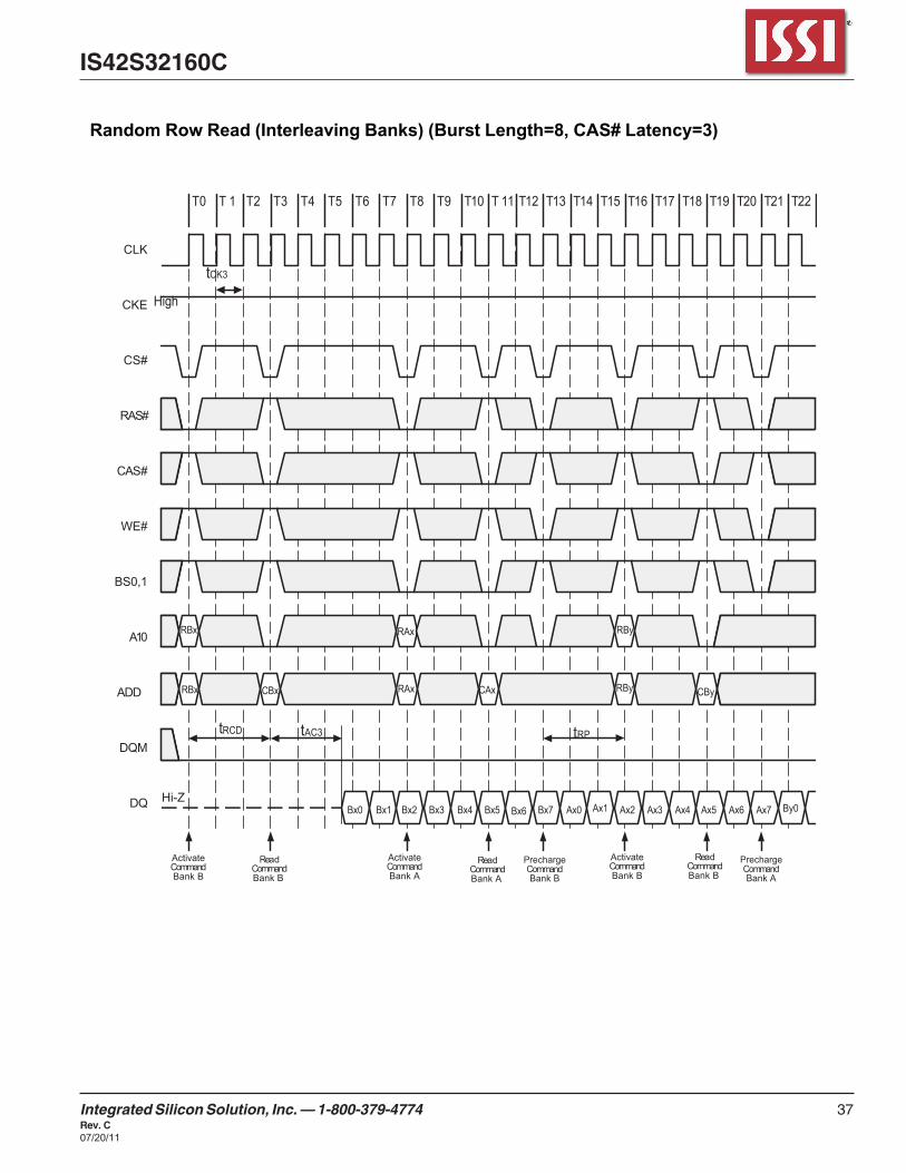
Random Row Read (Interleaving Banks) (Burst Length=8, CAS# Latency=3)
T0 T 1 T2 T3 T4 T5 T6 T7 T8 T9 T10 T 11 T12 T13 T14 T15 T16 T17 T18 T19 T20 T21 T22
tCK3
Bx0 Bx1 Bx2 Bx3 Bx4 Bx5 Bx6 Bx7 Ax0 Ax1
RBx
RBx RBy CBy
High
RAx
Ax7 By0Ax2 Ax3 Ax4 Ax5 Ax6
CBx CAxRAx
RBy
tRCD tAC3 tRP
CLK
CKE
CS#
RAS#
CAS#
WE#
BS0,1
A10
ADD
DQM
DQ Hi-Z
ActivateCommandBank A
ReadCommandBank A
PrechargeCommandBank A
ActivateCommandBank B
ActivateCommandBank B
ReadCommandBank B
ReadCommandBank B
PrechargeCommandBank B

38 Integrated Silicon Solution, Inc.Rev. C07/20/11
IS42S32160C
T0 T 1 T2 T3 T4 T5 T6 T7 T8 T9 T10 T 11 T12 T13 T14 T15 T16 T17 T18 T19 T20 T21 T22
tCK2
DAx0 DAx1 DAx2 DAx3 DAx4 DAx5 DAx6 DAx7 DBx0 DBx1
RAx
RAx RAy CAy
RBx
DBx7DBx2 DBx3 DBx4 DBx5 DBx6
CAx CBxRBx
RAy
tRCD
DAy3DAy0 DAy1 DAy2 DAy4
tWR* tRP tWR*
* tWR > tWR(min.)
CLK
CKE
CS#
RAS#
CAS#
WE#
BS0,1
A10
ADD
DQM
DQ Hi-Z
WriteCommandBank A
WriteCommandBank A
ActivateCommandBank A
ActivateCommandBank A
PrechargeCommandBank A
WriteCommandBank B
ActivateCommandBank B
PrechargeCommandBank B
High
Random Row Write (Interleaving Banks) (Burst Length=8, CAS# Latency=2)
Integrated Silicon Solution, Inc. — 1-800-379-4774 39Rev. C07/20/11
IS42S32160C
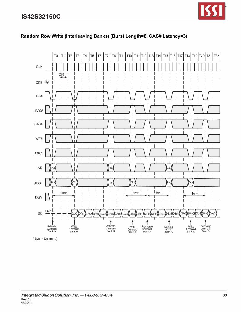
Random Row Write (Interleaving Banks) (Burst Length=8, CAS# Latency=3)
T0 T 1 T2 T3 T4 T5 T6 T7 T8 T9 T10 T 11 T12 T13 T14 T15 T16 T17 T18 T19 T20 T21 T22
tCK3
DAx0 DAx1 DAx2 DAx3 DAx4 DAx5 DAx6 DAx7 DBx0 DBx1
RAx
RAx RAy CAy
RBx
DBx7DBx2 DBx3 DBx4 DBx5 DBx6
CAx CBxRBx
RAy
tRCD
DAy3DAy0 DAy1 DAy2
tWR* tRP tWR*
* tWR > tWR(min.)
CLK
CKE
CS#
RAS#
CAS#
WE#
BS0,1
A10
ADD
DQM
DQHi-Z
WriteCommandBank A
WriteCommandBank A
ActivateCommandBank A
ActivateCommandBank A
PrechargeCommandBank A
WriteCommandBank B
ActivateCommandBank B
PrechargeCommandBank B
High

38 Integrated Silicon Solution, Inc.Rev. C07/20/11
IS42S32160C
T0 T 1 T2 T3 T4 T5 T6 T7 T8 T9 T10 T 11 T12 T13 T14 T15 T16 T17 T18 T19 T20 T21 T22
tCK2
DAx0 DAx1 DAx2 DAx3 DAx4 DAx5 DAx6 DAx7 DBx0 DBx1
RAx
RAx RAy CAy
RBx
DBx7DBx2 DBx3 DBx4 DBx5 DBx6
CAx CBxRBx
RAy
tRCD
DAy3DAy0 DAy1 DAy2 DAy4
tWR* tRP tWR*
* tWR > tWR(min.)
CLK
CKE
CS#
RAS#
CAS#
WE#
BS0,1
A10
ADD
DQM
DQ Hi-Z
WriteCommandBank A
WriteCommandBank A
ActivateCommandBank A
ActivateCommandBank A
PrechargeCommandBank A
WriteCommandBank B
ActivateCommandBank B
PrechargeCommandBank B
High
Random Row Write (Interleaving Banks) (Burst Length=8, CAS# Latency=2)

Integrated Silicon Solution, Inc. — 1-800-379-4774 41Rev. C07/20/11
IS42S32160C
Read and Write Cycle (Burst Length=4, CAS# Latency=3)
T0 T 1 T2 T3 T4 T5 T6 T7 T8 T9 T10 T 11 T12 T13 T14 T15 T16 T17 T18 T19 T20 T21 T22
tCK3
Ax0 Ax1 Ax2 Ax3 DAy0 DAy1 Az3DAy3 Az0 Az1
RAx
RAx CAx CAy CAz
CLK
CKE
CS#
RAS#
CAS#
WE#
BS0,1
A10
ADD
DQM
DQHi-Z
WriteCommandBank A
ActivateCommandBank A
ReadCommandBank A
ReadCommandBank A
The Write Datais Masked with a
Zero ClockLatency
The Read Datais Masked with a
Two ClockLatency

42 Integrated Silicon Solution, Inc.Rev. C07/20/11
IS42S32160C
T0 T 1 T2 T3 T4 T5 T6 T7 T8 T9 T10 T 11 T12 T13 T14 T15 T16 T17 T18 T19 T20 T21 T22
tCK2
Bw0 Bw1 Bx0 Bx1 By1 Ay0 Bz0
RAx
RAx
Ax0 Ax1 Ax2 Ax3 By0 Ay1 Bz1 Bz2 Bz3
tRCD tAC2
CAy RAx
RAx
CBw CBx CBy CAy CBz
CLK
CKE
CS#
RAS#
CAS#
WE#
BS0,1
A10
ADD
DQM
DQ Hi-Z
ActivateCommandBank A
ReadCommandBank A
ReadCommandBank A
PrechargeCommandBank A
ActivateCommandBank B
ReadCommandBank B
ReadCommandBank B
ReadCommandBank B
ReadCommandBank B
PrechargeCommandBank B
Interleaving Column Read Cycle (Burst Length=4, CAS# Latency=2)

Integrated Silicon Solution, Inc. — 1-800-379-4774 43Rev. C07/20/11
IS42S32160C
T0 T 1 T2 T3 T4 T5 T6 T7 T8 T9 T10 T 11 T12 T13 T14 T15 T16 T17 T18 T19 T20 T21 T22
tCK3
Bx0 Bx1 By0 By1 Bz1 Ay0 Ay2
RAx
RAx
Ax0 Ax1 Ax2 Ax3 Bz0 Ay1 Ay3
tRCD tAC3
CAx RBx
RBx
CBx CBy CBz CAy
CLK
CKE
CS#
RAS#
CAS#
WE#
BS0,1
A10
ADD
DQM
DQ Hi-Z
ActivateCommandBank A
ReadCommandBank A
ReadCommandBank A
PrechargeCommandBank A
ActivateCommandBank B
ReadCommandBank B
ReadCommandBank B
ReadCommandBank B
PrechargeCommandBank B
Interleaved Column Read Cycle (Burst Length=4, CAS# Latency=3)

44 Integrated Silicon Solution, Inc.Rev. C07/20/11
IS42S32160C
T0 T 1 T2 T3 T4 T5 T6 T7 T8 T9 T10 T 11 T12 T13 T14 T15 T16 T17 T18 T19 T20 T21 T22
tCK2
DBx0 DBx1 DAy0
RAx
RAx
DAx0 DAx1 DAx2 DAx3 DAy1
tRCD
CAx RBw
RBw
CBw CBx CBy CAy
tRRD
tRP tWR tRP
CBz
DBz0 DBz1 DBz2 DBz3DBy0 DBy1DBw0 DBw1
CLK
CKE
CS#
RAS#
CAS#
WE#
BS0,1
A10
ADD
DQM
DQHi-Z
WriteCommandBank A
WriteCommandBank A
ActivateCommandBank A
PrechargeCommandBank A
WriteCommandBank B
WriteCommandBank B
WriteCommandBank B
WriteCommandBank B
ActivateCommandBank B
PrechargeCommandBank B
Interleaved Column Write Cycle (Burst Length=4, CAS# Latency=2)

Integrated Silicon Solution, Inc. — 1-800-379-4774 45Rev. C07/20/11
IS42S32160C
Interleaved Column Write Cycle (Burst Length=4, CAS# Latency=3)
T0 T 1 T2 T3 T4 T5 T6 T7 T8 T9 T10 T 11 T12 T13 T14 T15 T16 T17 T18 T19 T20 T21 T22
tCK3
DBw0 DBw1 DBx0 DBx1 DBy1 DAy0
RAx
RAx
DAx0 DAx1 DAx2 DAx3 DBy0 DAy1
tRCD
CAx RBw
RBw
CBw CBx CBy CAy
tRRD > tRRD(min)
tRPtWR tWR(min)
CBz
DBz0 DBz1 DBz2 DBz3
CLK
CKE
CS#
RAS#
CAS#
WE#
BS0,1
A10
ADD
DQM
DQHi-Z
WriteCommandBank A
WriteCommandBank A
ActivateCommandBank A
PrechargeCommandBank A
WriteCommandBank B
WriteCommandBank B
WriteCommandBank B
WriteCommandBank B
ActivateCommandBank B
PrechargeCommandBank B

46 Integrated Silicon Solution, Inc.Rev. C07/22/11
IS42S32160C
Auto Precharge after Read Burst (Burst Length=4, CAS# Latency=2)
T0 T 1 T2 T3 T4 T5 T6 T7 T8 T9 T10 T 11 T12 T13 T14 T15 T16 T17 T18 T19 T20 T21 T22
tCK2
Bx0 Bx1 Bx2 Bx3 Ay1 Ay2
RAx
RAx
RBx
Ax0 Ax1 Ax2 Ax3 Ay0 Ay3 By0
RBx CBx RByRAy CBy
By1 By2 By3 Az0 Az1 Az2
CAx
RBy RAz
CAzRAz
CLK
CKE
CS#
RAS#
CAS#
WE#
BS0,1
A10
ADD
DQM
DQHi-Z
ActivateCommandBank A
ActivateCommandBank A
ReadCommandBank A
ActivateCommandBank B
ActivateCommandBank B
High
Read withAuto Precharge
CommandBank B
Read withAuto Precharge
CommandBank B
Read withAuto Precharge
CommandBank A
Read withAuto Precharge
CommandBank A

Integrated Silicon Solution, Inc. — 1-800-379-4774 47Rev. C07/20/11
IS42S32160C
Auto Precharge after Read Burst (Burst Length=4, CAS# Latency=3)
T0 T 1 T2 T3 T4 T5 T6 T7 T8 T9 T10 T 11 T12 T13 T14 T15 T16 T17 T18 T19 T20 T21 T22
tCK3
Bx0 Bx1 Bx2 Bx3 Ay1 Ay2
RAx
RAx
RBx
Ax0 Ax1 Ax2 Ax3 Ay0 Ay3 By0
RBx CBx
By1 By2 By3
CAx
RBy
CByRByCAy
CLK
CKE
CS#
RAS#
CAS#
WE#
BS0,1
A10
ADD
DQM
DQHi-Z
ActivateCommandBank A
ReadCommandBank A
ActivateCommandBank B
ActivateCommandBank B
High
Read withAuto Precharge
CommandBank B
Read withAuto Precharge
CommandBank BRead with
Auto PrechargeCommandBank A

48 Integrated Silicon Solution, Inc.Rev. C07/20/11
IS42S32160C
Auto Precharge after Write Burst (Burst Length=4, CAS# Latency=2)
T0 T 1 T2 T3 T4 T5 T6 T7 T8 T9 T10 T 11 T12 T13 T14 T15 T16 T17 T18 T19 T20 T21 T22
tCK2
DBx0 DBx1 DBx2 DBx3 DAy1 DAy2
RAx
RAx
RBx
DAx0 DAx1 DAx2 DAx3 DAy0 DAy3
CBx CAy
RBy
CByRBy
DAz0 DAz1 DAz2 DAz3
CAx RBx CAz
RAz
RAz
DBy0 DBy1 DBy2 DBy3
CLK
CKE
CS#
RAS#
CAS#
WE#
BS0,1
A10
ADD
DQM
DQ Hi-Z
WriteCommandBank A
ActivateCommandBank A
ActivateCommandBank A
ActivateCommandBank B
ActivateCommandBank B
High
Write withAuto Precharge
CommandBank B
Write withAuto Precharge
CommandBank B
Write withAuto Precharge
CommandBank A
Write withAuto Precharge
CommandBank A

Integrated Silicon Solution, Inc. — 1-800-379-4774 49Rev. C07/21/11
IS42S32160C
Auto Precharge after Write Burst (Burst Length=4, CAS# Latency=3)
T0 T 1 T2 T3 T4 T5 T6 T7 T8 T9 T10 T 11 T12 T13 T14 T15 T16 T17 T18 T19 T20 T21 T22
tCK3
DBx0 DBx1 DBx2 DBx3 DAy1 DAy2
RAx
RAx
RBx
DAx0 DAx1 DAx2 DAx3 DAy0 DAy3
CBx CAyCAx RBx CBy
RBy
RBy
‘
DBy0 DBy1 DBy2 DBy3
CLK
CKE
CS#
RAS#
CAS#
WE#
BS0,1
A9
ADD
DQM
DQHi-Z
WriteCommandBank A
ActivateCommandBank A
ActivateCommandBank B
ActivateCommandBank B
High
Write withAuto Precharge
CommandBank B
Write withAuto Precharge
CommandBank B
Write withAuto Precharge
CommandBank A

50 Integrated Silicon Solution, Inc.Rev. C07/20/11
IS42S32160C
Full Page Read Cycle (Burst Length=Full Page, CAS# Latency=2)
T0 T 1 T2 T3 T4 T5 T6 T7 T8 T9 T10 T 11 T12 T13 T14 T15 T16 T17 T18 T19 T20 T21 T22
Ax Ax+1 Bx Bx+1 Bx+3 Bx+4
RAx
RAx
Ax+1 Ax+2 Ax-2 Ax-1 B x+2 Bx+5
CBxRBxCAx RBy
RBy
Ax Bx+6
tCK2
tRP
RBx
CLK
CKE
CS#
RAS#
CAS#
WE#
BS0,1
A10
ADD
DQM
DQHi-Z
ActivateCommandBank A
ActivateCommandBank B
ActivateCommandBank B
PrechargeCommandBank B
High
Burst StopCommand
The burst counter wrapsfrom the highest orderpage address back to zeroduring this time interval
ReadCommandBank A
ReadCommandBank B
Full Page burst operation does notterm in ate when the burst length is sat is fied;the burst counter increments and continuesbursting beginning with the starting address.

Integrated Silicon Solution, Inc. — 1-800-379-4774 51Rev. C07/20/11
IS42S32160C
Full Page Read Cycle (Burst Length=Full Page, CAS# Latency=3)
T0 T 1 T2 T3 T4 T5 T6 T7 T8 T9 T10 T 11 T12 T13 T14 T15 T16 T17 T18 T19 T20 T21 T22
Bx Bx+1
RAx
RAx
Ax+1 Ax-2 Ax-1
CBxRBxCAx RBy
RBy
Ax
tCK3
tRP
RBx
Ax+2 Ax Ax+1 Bx+2 Bx+3 Bx+4 Bx+5
CLK
CKE
CS#
RAS#
CAS#
WE#
BS0,1
A10
ADD
DQM
DQ Hi-Z
ActivateCommandBank A
ActivateCommandBank B
ActivateCommandBank B
PrechargeCommandBank B
High
Burst StopCommand
The burst counter wrapsfrom the highest orderpage address back to zeroduring this time interval
ReadCommandBank A
ReadCommandBank B
Full Page burst operation does notterminate when the burst length issatisfied; the burst counterincrements and continuesbursting beginning with thestarting address.

52 Integrated Silicon Solution, Inc.Rev. C07/20/11
IS42S32160C
Full Page Write Cycle (Burst Length=Full Page, CAS# Latency=2)
T0 T 1 T2 T3 T4 T5 T6 T7 T8 T9 T10 T 11 T12 T13 T14 T15 T16 T17 T18 T19 T20 T21 T22
RAx
RAx CBxRBxCAx RBy
RBy
tCK2
5
RBx
DAx DAx+1 DAx+2 DAx+3 DAx-1 DAx DAx+1 DBx DBx+1 DBx+2 DBx+3 DBx+4 DBx+5 DBx+6
CLK
CKE
CS#
RAS#
CAS#
WE#
BS0,1
A10
ADD
DQM
DQHi-Z
WriteCommandBank A
ActivateCommandBank A
WriteCommandBank B
ActivateCommandBank B
ActivateCommandBank B
PrechargeCommandBank B
High
Burst StopCommand
Data is ignored
Full Page burst operation doesnot terminate when the burstlength is satisfied; the burst counterincrements and continues burstingbeginning with the starting address.
The burst counter wrapsfrom the highest orderpage address back to zeroduring this time interval

Integrated Silicon Solution, Inc. — 1-800-379-4774 53Rev. C07/20/11
IS42S32160C
Full Page Write Cycle (Burst Length=Full Page, CAS# Latency=3)
T0 T 1 T2 T3 T4 T5 T6 T7 T8 T9 T10 T 11 T12 T13 T14 T15 T16 T17 T18 T19 T20 T21 T22
RAx
RAx CBxRBxCAx RBy
RBy
tCK3
RBx
Data is ignored
DAx DAx+1 DAx+2 DAx+3 DAx-1 DAx DAx+1 DBx DBx+1 DBx+3 DBx+4 DBx+5
CLK
CKE
CS#
RAS#
CAS#
WE#
BS0,1
A10
ADD
DQM
DQHi-Z
High
WriteCommandBank A
ActivateCommandBank A
WriteCommandBank B
ActivateCommandBank B
The burst counter wrapsfrom the highest orderpage address back to zeroduring this time interval
ActivateCommandBank B
PrechargeCommandBank B
Burst StopCommand
Full Page burst operation doesnot terminate when the burstlength is satisfied; the burst counterincrements and continues burstingbeginning with the starting address.

54 Integrated Silicon Solution, Inc.Rev. C07/20/11
IS42S32160C
Byte Write Operation (Burst Length=4, CAS# Latency=2)
T0 T 1 T2 T3 T4 T5 T6 T7 T8 T9 T10 T 11 T12 T13 T14 T15 T16 T17 T18 T19 T20 T21 T22
RAx
RAx CAyCAx
tCK2
CAz
Ax0 Ax1 Ax2
Ax1 Ax2 Ax3
DAy1 DAy2
DAy0 DAy1 DAy3
Az1 Az2
Az1 Az2 Az3
WriteCommandBank A
CLK
CKE
CS#
RAS#
CAS#
WE#
BS0,1
A10
ADD
High
ActivateCommandBank A
CommandBank A
DQM0
DQM1,2,3
DQ0 - DQ7
DQ8 - DQ15
ReadCommandBank A
Readare masked
Upper 3 Bytesare masked
Upper 3 BytesLower Byteis masked Lower Byte
is maskedLower Byteis masked

Integrated Silicon Solution, Inc. — 1-800-379-4774 55Rev. C07/20/11
IS42S32160C
Full Page Random Column Read (Burst Length=Full Page, CAS# Latency=2)
T0 T 1 T2 T3 T4 T5 T6 T7 T8 T9 T10 T 11 T12 T13 T14 T15 T16 T17 T18 T19 T20 T21 T22
tCK2
Ax0 Bx0 Ay0 Ay1 By0 By1 Az0 Az1 Az2 Bz0 Bz1 Bz2
t RP
tRRD tRCD
RAx
RAx
RBx
RBx CAx CBx CAy CBy CAz CBz
RBw
RBw
CLK
CKE
CS#
RAS#
CAS#
WE#
BS0,1
A10
ADD
DQM
DQ
CommandBank B
ActivateCommandBank A
ActivateCommandBank B
ActivateCommandBank B
ReadCommandBank B
ReadCommandBank B
Read
CommandBank A
Read CommandBank A
Read
CommandBank A
Read PrechargeCommand Bank B
(Precharge Temination)

56 Integrated Silicon Solution, Inc.Rev. C07/20/11
IS42S32160C
Full Page Random Column Write (Burst Length=Full Page, CAS# Latency=2)
T0 T 1 T2 T3 T4 T5 T6 T7 T8 T9 T10 T 11 T12 T13 T14 T15 T16 T17 T18 T19 T20 T21 T22
tCK2
DAx0 DBx0 DAy0 DAy1 DBy0 DBy1 DAz0 DAz1 DAz2 DBz0
t RP
tRRD tRCD
RAx
RAx
RBx
RBx CAx CBx CAy CBy CAz CBz
RBw
RBw
tWR
DBz1 DBz2
CLK
CKE
CS#
RAS#
CAS#
WE#
BS0,1
A10
ADD
DQM
DQ
WriteCommandBank A
WriteCommandBank A
WriteCommandBank A
ActivateCommandBank A
WriteCommandBank B
WriteCommandBank B
WriteCommandBank B
ActivateCommandBank B
ActivateCommandBank B
PrechargeCommand Bank B
(Precharge Temination)
Write Datais masked

Integrated Silicon Solution, Inc. — 1-800-379-4774 57Rev. C07/20/11
IS42S32160C
Precharge Termination of a Burst (Burst Length=8 or Full Page, CAS# Latency=2)
T0 T 1 T2 T3 T4 T5 T6 T7 T8 T9 T10 T 11 T12 T13 T14 T15 T16 T17 T18 T19 T20 T21 T22
tCK2
DAx0 DAx1 DAx2 DAx3 Ay2Ay0 Ay1
RAx
RAx
RAy
CAx RAy CAy
Az0 Az1 Az2
tWR tRP tRP
RAz
CAz
tRP
RAz
CLK
CKE
CS#
RAS#
CAS#
WE#
BS0,1
A10
ADD
DQM
DQ
High
WriteCommandBank A
ActivateCommandBank A
ActivateCommandBank A
ActivateCommandBank A
CommandBank A
PrechargeCommandBank A
PrechargeCommandBank A
PrechargeCommandBank A
ReadCommandBank A
Read
Precharge Terminationof a Write Burst.
Precharge Terminationof a Read Burst.Write data is masked.

58 Integrated Silicon Solution, Inc.Rev. C07/20/11
IS42S32160C
Precharge Termination of a Burst (Burst Length=4,8 or Full Page, CAS# Latency=3)
T0 T 1 T2 T3 T4 T5 T6 T7 T8 T9 T10 T 11 T12 T13 T14 T15 T16 T17 T18 T19 T20 T21 T22
tCK3
DAx0 Ay0 Ay1 Ay2
RAx
RAx
RAy
CAx RAy CAy
t WR tRP tRP
RAz
RAz
DAx1
CLK
CKE
CS#
RAS#
CAS#
WE#
BS0,1
A10
ADD
DQM
DQ
High
WriteCommandBank A
CommandBank A
ActivateCommandBank A
ActivateCommandBank A
ActivateCommandBank A
PrechargeCommandBank A
PrechargeCommandBank A
Write Datais masked Precharge Termination
of a Write Burst
Precharge Terminationof a Read Burst
Read

Integrated Silicon Solution, Inc. 59Rev. C07/20/11
IS42S32160C
ORDERING INFORMATION - Vdd = 3.3V
Commercial Range: 0°C to 70°C Frequency Speed (ns) Order Part No. Package
133MHz 7.5 IS42S32160C-75BL 8x13mmBGA,Lead-free
166MHz 6.0 IS42S32160C-6BL 8x13mmBGA,Lead-free
Industrial Range: -40°C to 85°C Frequency Speed (ns) Order Part No. Package
133MHz 7.5 IS42S32160C-75BLI 8x13mmBGA,Lead-free
166MHz 6.0 IS42S32160C-6BI 8x13mmBGA
166MHz 6.0 IS42S32160C-6BLI 8x13mmBGA,Lead-free

2. R
efer
ence
doc
umen
t : J
ED
EC
MS
-207
1. C
ON
TRO
LLIN
G D
IME
NS
ION
: M
M .
NO
TE :
08/2
8/20
08Pa
ckag
e O
utlin
e