failure mechanism of fbga solder joints in memory module ...prem.hanyang.ac.kr/down/failure...
TRANSCRIPT

Microelectronics Reliability 52 (2012) 735–743
Contents lists available at SciVerse ScienceDirect
Microelectronics Reliability
journal homepage: www.elsevier .com/locate /microrel
Failure mechanism of FBGA solder joints in memory module subjected toharmonic excitation
Yusuf Cinar a, Jinwoo Jang a, Gunhee Jang a,⇑, Seonsik Kim b, Jaeseok Jang b, Jinkyu Chang b, Yonghyun Jun b
a Department of Mechanical Engineering, Hanyang University, 17, Haengdang-dong, Seongdong-gu, Seoul 133-791, Republic of Koreab Memory Division, Samsung Electronics Co. Ltd., San #16, Banwol-Ri, Taean-Eup, Hwasung-City, Gyeonggi-Do 445-701, Republic of Korea
a r t i c l e i n f o
Article history:Received 7 October 2010Received in revised form 2 November 2011Accepted 23 November 2011Available online 20 December 2011
0026-2714/$ - see front matter � 2011 Elsevier Ltd. Adoi:10.1016/j.microrel.2011.11.015
⇑ Corresponding author. Address: PREM, DepartmenHanyang University, 17, Haengdang-dong, Seongdongof Korea. Tel.: +82 2 2299 5685; fax: +82 2 2292 340
E-mail address: [email protected] (G. Jang).
a b s t r a c t
This paper investigates the failure mechanism of Fine-pitch Ball Grid Array (FBGA) solder joints of mem-ory modules due to harmonic excitation by the experiments and the finite element method. A finite ele-ment model of the memory module was developed, and the natural frequencies and modes werecalculated and verified by experimental modal testing. Modal damping ratios are also obtained and usedin the forced vibration analysis. The experimental setup was developed to monitor resistance variation ofFBGA solder joints due to the harmonic excitation under Joint Electron Devices Engineering Council(JEDEC) standard service conditions. Experiments showed that the failure of the solder joints of the mem-ory module under vibration mainly occurs due to resonance. Forced vibration analysis was performed todetermine the solder joints having high stress concentration under harmonic excitation. It showed thatfailure occurs due to the relative displacement between PCB and package and solder joints are the mostvulnerable part of the memory module under vibration. It also showed that cracked solder joints in theexperiments match those in the simulations with the highest stress concentration.
� 2011 Elsevier Ltd. All rights reserved.
1. Introduction
Memory modules are composed of a number of packages or dy-namic random access memory integrated circuits modulesmounted on a printed circuit board (PCB), designed for use in per-sonal computers, workstations, and servers. There are varioustypes of memory modules, such as Single In-Line Memory Module(SIMM), Dual In-Line Memory Module (DIMM), and Small OutlineDual In-Line Memory Module (SO-DIMM). Packages are mountedon PCBs through solder balls called ball grid arrays (BGAs). Solderballs are further used to provide the electrical signals betweenpackage chips and the PCB. Memory modules are exposed to vibra-tion over various frequency ranges [1], which may result in themalfunction of products. Reliability and performance of memorymodules are standardized by the Joint Electron Devices Engineer-ing Council (JEDEC). Performance and fatigue life time of the mem-ory modules mostly depend on the solder joints. According to areport released by a semiconductor company, solder joint cracksreflected approximately 40% of total failure of memory modules.Therefore, it is important to understand the dynamic behavior ofmemory modules, as well as the behavior of solder joints subjectedto vibration.
ll rights reserved.
t of Mechanical Engineering,-gu, Seoul 133-791, Republic6.
Many researchers have investigated the fatigue life reliability ofpackages or memory modules due to thermal load by experimentand simulation [2–4]. Once vibration was realized to be one ofthe dominant failures for electronic components, the electronicpackaging industry began to show interest in understanding itsfailure mechanism under vibration. Basaran and Chandaroy [5]presented a study based on a viscoplastic model to compute dam-age mechanics of a solder joint with Pb40/Sn60 solder alloys underdifferent dynamic load conditions. They showed that fatigue life ofsolder alloys is greatly affected by dynamic loads and the fre-quency ranges of applied loads. Kim et al. [6] investigated the highcycle vibration fatigue life characteristics of Pb-free and Pb pack-ages under various mixed mode stresses by experiment and FEM.They observed the failure process of a solder ball at low frequencyduring the fatigue test by using an optical microscope. Wu [7] uti-lized the global–local modeling concept to calculate von Misesstress in solder joints of interest under random vibration loading.Then, she predicted the fatigue life of solder joints by using a dam-age model, called the Basquin power-law relation. Che and Pang [8]studied flip chip solder joints under out-of-plane sinusoidal vibra-tion load with constant and varying amplitudes and they usedMiner’s cumulative damage law to estimate fatigue life of flip chipsolder joints. Zhou et al. [9,10] investigated the vibration durabilityof Sn3.0Ag0.5Cu (SAC305) and Sn37Pb solder interconnects undernarrow-band harmonic vibration and random vibration. Theyfound that SAC305 interconnects have lower fatigue durabilitythan Sn37Pb interconnects. However, prior researchers did not

Fig. 1. A DDR3 SDRAM type memory module: (a) front view, (b) back view and (c) side view.
Table 1Dimensions of bare PCB and packages of a memory module.
Components Number of components (EA) Dimensions in mm (L �W � H)
Bare PCB 1 133.35 � 30.00 � 1.295Package 36 11.00 � 7.50 � 0.77Package register 1 13.50 � 8.00 � 0.779
736 Y. Cinar et al. / Microelectronics Reliability 52 (2012) 735–743
investigate failure mechanism of the solder joint in terms of resis-tance variation over high frequency ranges, as well as the most vul-nerable solder joint of the memory module under vibration.
This paper investigates the failure mechanism of Fine-pitch BallGrid Array (FBGA) solder joints in daisy chains assembled memorymodule with double-sided packages due to harmonic excitation byusing the experiments and the finite element method. The experi-mental setup was developed to monitor resistance variation ofFBGA solder joints due to the harmonic excitation of the JEDECstandard service condition 1 [11]. A finite element model of thememory module was developed, and the natural frequencies andmodes were calculated and verified by experimental modal testing.Forced vibration analysis was performed to correlate the crackedsolder joints in experiments with the solder joint of high stressconcentration in simulation.
Fig. 2. BGA patterns of package and package register: (a) package and (b) packageregister.
2. Analysis model
Fig. 1 shows a double-data-rate three synchronous dynamicrandom access memory (DDR3 SDRAM) type memory module usedin this research. It is mainly composed of a PCB, packages and pack-age register, and solder balls. The PCB is composed of 10 layers ofcopper conductor and FR-4, while the packages and package regis-ter are composed of many integrated circuits (ICs). This memorymodule has 36 packages and 1 package register. Table 1 showsthe mechanical dimensions of PCB, package, and package register.
There are two types of solder balls used in the packages and thepackage register. The solder balls of the packages and the packageregister have diameters of 0.4 mm and 0.3 mm and heights of

Fig. 3. Finite element model of a memory module: (a) front view, (b) back view and (c) side view.
Table 2Material properties of each component of a memory module.
Component Material type Density (kg m�3) Young’s modulus (MPa) Poisson’s ratio (–) Element type Element number
Bare PCB FR4 2200.5 22,000 0.40 Brick 78,368Package – 1920.5 12,000 0.40 Brick 77,184Package register – 2389.1 12,000 0.40 Brick 6964Solder ball Sn–Ag–Cu 7094.0 44,113 0.36 Brick 46,337
Fig. 4. Experimental setup for modal testing.
Y. Cinar et al. / Microelectronics Reliability 52 (2012) 735–743 737
0.3079 mm and 0.3026 mm, respectively. Solder balls are modeledas an octagonal structure with sixteen elements. The BGAs of thepackage and package register have different patterns, as shownin Fig. 2. The red square1 in package and package register inFig. 2 shows their orientation in memory module in Fig. 1.
1 For interpretation of color in Figs. 1–3,8,9, the reader is referred to the webversion of this article.
3. Free vibration analysis
A finite element model of the memory module was developed,as shown in Fig. 3. Table 2 shows the material type, properties, ele-ment type and number of each component. The PCB, packages,package register, and solder balls are modeled by the linear brickelements with eight nodes, and each node has three degrees offreedom. The total number of elements was 208,853. In the finiteelement model, packages, solder balls and PCB were connected
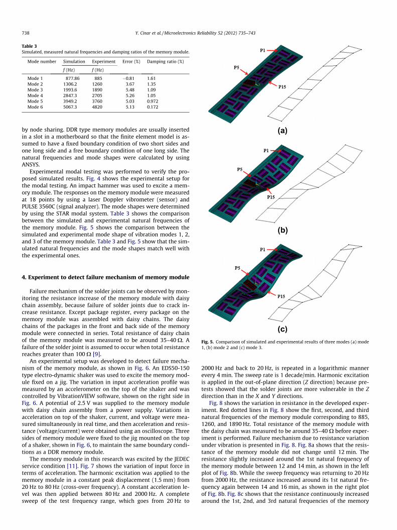
Table 3Simulated, measured natural frequencies and damping ratios of the memory module.
Mode number Simulation Experiment Error (%) Damping ratio (%)
f (Hz) f (Hz)
Mode 1 877.86 885 �0.81 1.61Mode 2 1306.2 1260 3.67 1.35Mode 3 1993.6 1890 5.48 1.09Mode 4 2847.3 2705 5.26 1.05Mode 5 3949.2 3760 5.03 0.972Mode 6 5067.3 4820 5.13 0.172
738 Y. Cinar et al. / Microelectronics Reliability 52 (2012) 735–743
by node sharing. DDR type memory modules are usually insertedin a slot in a motherboard so that the finite element model is as-sumed to have a fixed boundary condition of two short sides andone long side and a free boundary condition of one long side. Thenatural frequencies and mode shapes were calculated by usingANSYS.
Experimental modal testing was performed to verify the pro-posed simulated results. Fig. 4 shows the experimental setup forthe modal testing. An impact hammer was used to excite a mem-ory module. The responses on the memory module were measuredat 18 points by using a laser Doppler vibrometer (sensor) andPULSE 3560C (signal analyzer). The mode shapes were determinedby using the STAR modal system. Table 3 shows the comparisonbetween the simulated and experimental natural frequencies ofthe memory module. Fig. 5 shows the comparison between thesimulated and experimental mode shape of vibration modes 1, 2,and 3 of the memory module. Table 3 and Fig. 5 show that the sim-ulated natural frequencies and the mode shapes match well withthe experimental ones.
Fig. 5. Comparison of simulated and experimental results of three modes (a) mode1, (b) mode 2 and (c) mode 3.
4. Experiment to detect failure mechanism of memory module
Failure mechanism of the solder joints can be observed by mon-itoring the resistance increase of the memory module with daisychain assembly, because failure of solder joints due to crack in-crease resistance. Except package register, every package on thememory module was assembled with daisy chains. The daisychains of the packages in the front and back side of the memorymodule were connected in series. Total resistance of daisy chainof the memory module was measured to be around 35–40 X. Afailure of the solder joint is assumed to occur when total resistancereaches greater than 100 X [9].
An experimental setup was developed to detect failure mecha-nism of the memory module, as shown in Fig. 6. An EDS50-150type electro-dynamic shaker was used to excite the memory mod-ule fixed on a jig. The variation in input acceleration profile wasmeasured by an accelerometer on the top of the shaker and wascontrolled by VibrationVIEW software, shown on the right side inFig. 6. A potential of 2.5 V was supplied to the memory modulewith daisy chain assembly from a power supply. Variations inacceleration on top of the shaker, current, and voltage were mea-sured simultaneously in real time, and then acceleration and resis-tance (voltage/current) were obtained using an oscilloscope. Threesides of memory module were fixed to the jig mounted on the topof a shaker, shown in Fig. 6, to maintain the same boundary condi-tions as a DDR memory module.
The memory module in this research was excited by the JEDECservice condition [11]. Fig. 7 shows the variation of input force interms of acceleration. The harmonic excitation was applied to thememory module in a constant peak displacement (1.5 mm) from20 Hz to 80 Hz (cross-over frequency). A constant acceleration le-vel was then applied between 80 Hz and 2000 Hz. A completesweep of the test frequency range, which goes from 20 Hz to
2000 Hz and back to 20 Hz, is repeated in a logarithmic mannerevery 4 min. The sweep rate is 1 decade/min. Harmonic excitationis applied in the out-of-plane direction (Z direction) because pre-tests showed that the solder joints are more vulnerable in the Zdirection than in the X and Y directions.
Fig. 8 shows the variation in resistance in the developed exper-iment. Red dotted lines in Fig. 8 show the first, second, and thirdnatural frequencies of the memory module corresponding to 885,1260, and 1890 Hz. Total resistance of the memory module withthe daisy chain was measured to be around 35–40 X before exper-iment is performed. Failure mechanism due to resistance variationunder vibration is presented in Fig. 8. Fig. 8a shows that the resis-tance of the memory module did not change until 12 min. Theresistance slightly increased around the 1st natural frequency ofthe memory module between 12 and 14 min, as shown in the leftplot of Fig. 8b. While the sweep frequency was returning to 20 Hzfrom 2000 Hz, the resistance increased around its 1st natural fre-quency again between 14 and 16 min, as shown in the right plotof Fig. 8b. Fig. 8c shows that the resistance continuously increasedaround the 1st, 2nd, and 3rd natural frequencies of the memory
Fig. 6. Experimental setup to monitor failure mechanism.
Fig. 7. Variation of acceleration input of JEDEC service condition 1.
Y. Cinar et al. / Microelectronics Reliability 52 (2012) 735–743 739
module between 28 and 32 min. Finally, the resistance of thememory module at the 1st natural frequency increased bigger than100 X between 44 and 48 min, as shown in Fig. 8d. Crack growthreduces stiffness of the memory module, which decreases naturalfrequency of the memory module. As the experiment goes by, fre-quency range at which resistance increases near natural frequen-cies gradually becomes wider as shown in Fig. 8.
In this work, the same experiment was performed for six mem-ory modules with daisy chains. Time to failure is approximately45–55 min, and packages near the fixed boundary shown inFig. 5 were the frequently failed packages. One of the most fre-quently failed packages is the package 5 and 33 shown in Fig. 1.Crack propagation is also found in package 1. Fig. 9 shows thecross-sectional view of the solder ball of packages 1 and 5 of thememory module after the molding, cutting, and polishing process.The crack in the solder ball is located near the PCB side.
5. Finite element forced vibration analysis
The dynamic response of a memory module subjected to har-monic excitation was investigated by using the finite element
method and mode superposition. The damped global finite elementequation of the memory module due to harmonic excitation is gi-ven by
½M�f€xðtÞg þ ½C�f _xðtÞg þ ½K�fxðtÞg ¼ fPðtÞg ð1Þ
where [M], [C], [K] and {P(t)} are the mass, damping, stiffness matri-ces and excitation force vector, and f€xðtÞg, f _xðtÞg and {x(t)} are thenodal acceleration, velocity and displacement vectors. In the largesized problem, the direct integration technique to obtain the forcedresponse is not the computationally efficient method [12]. Theforced response, {x(t)}, can be approximated by using the modesuperposition method as follows:
fxðtÞg �Xn
i¼1
f/igfziðtÞg ð2Þ
where {/i} is the i-th mode vector which is the eigenvector calcu-lated by the free vibration analysis. {zi(t)} and n are modal displace-ment and the number of modes to be used in calculation of thedisplacement vector, {x(t)}, respectively. Substituting Eqs. (2) into(1) and rearranging it after multiplying with {/i}T
, the decoupledn equations of motion are obtained as follows:
½U�T ½M�½U�f€zg þ ½U�T ½C�½U�f _zg þ ½U�T ½K�½U�fzg ¼ ½U�TfPg ð3Þ
Then Eq. (3) can be written in terms of modal coordinates asfollows:
€zi þ 2xini _zi þx2i zi ¼ Q iði ¼ 1 . . . nÞ ð4Þ
where xi and ni donate natural frequency and damping ratio ofi-th mode, respectively. Eq. (4) becomes a set of n decoupled dif-ferential equations for the damped system and the solution interms of modal coordinate, zi, can be obtained by using the timeintegration. Then the displacement, {x(t)}, can be calculated withthe Eq. (2).
Frequency response of a memory module was obtained experi-mentally, and the half power method was used to calculate modaldamping ratios of the memory module from Eq. (5) for its sixmodes shown in Table 3 [13]. They were inserted into Eq. (4).

Fig. 8. Variation of the resistance of the memory module during the harmonic excitation of the JEDEC service condition 1: (a) from 0 to 12 min, (b) from 12 to 16 min, (c) from28 to 32 min and (d) from 44 to 48 min.
740 Y. Cinar et al. / Microelectronics Reliability 52 (2012) 735–743
ni ¼12
Dxxi
ð5Þ
where Dx is the width of the frequency response curve at the halfpower level.
The harmonic excitation force of JEDEC service condition 1 canbe written as follows:
pðtÞ ¼ p_ðtÞ sinxðtÞ ð6Þ
In the case of logarithmic sweep, the variation of frequency with re-spect to time is given by
xðtÞ ¼ xs23:3219St=60 ð7Þ
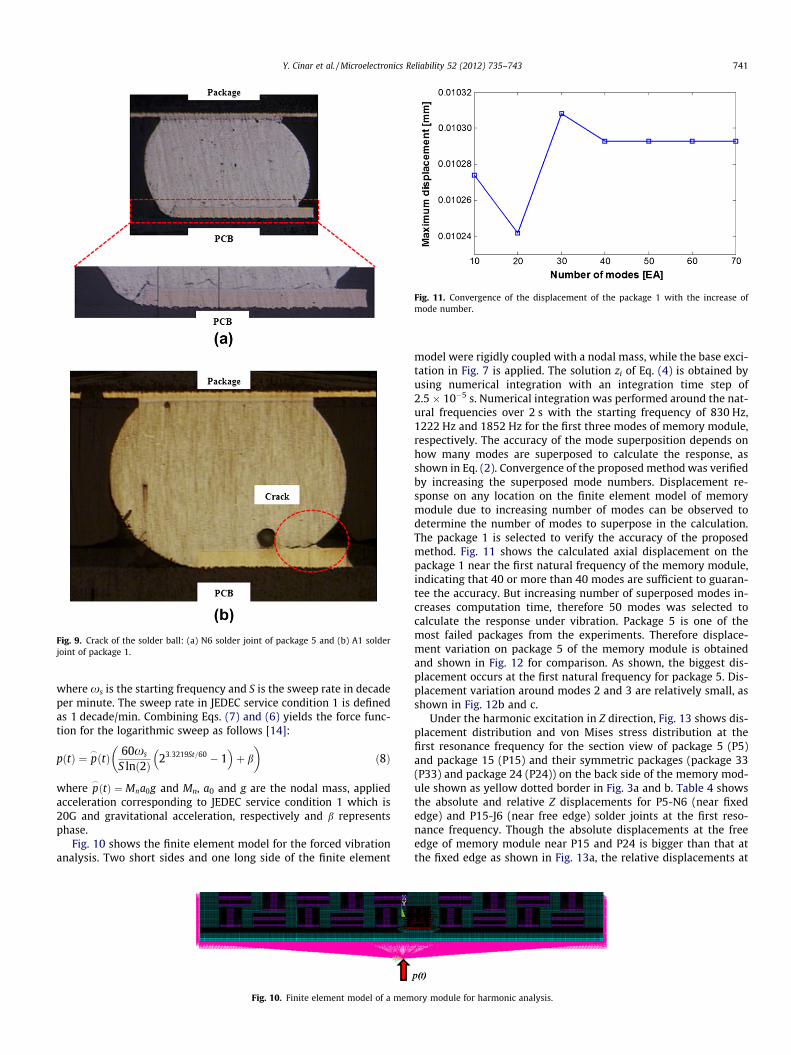
Fig. 9. Crack of the solder ball: (a) N6 solder joint of package 5 and (b) A1 solderjoint of package 1.
Fig. 11. Convergence of the displacement of the package 1 with the increase ofmode number.
Y. Cinar et al. / Microelectronics Reliability 52 (2012) 735–743 741
where xs is the starting frequency and S is the sweep rate in decadeper minute. The sweep rate in JEDEC service condition 1 is definedas 1 decade/min. Combining Eqs. (7) and (6) yields the force func-tion for the logarithmic sweep as follows [14]:
pðtÞ ¼ p_ðtÞ 60xs
S lnð2Þ 23:3219St=60 � 1� �
þ b
� �ð8Þ
where p_ðtÞ ¼ Mna0g and Mn, a0 and g are the nodal mass, applied
acceleration corresponding to JEDEC service condition 1 which is20G and gravitational acceleration, respectively and b representsphase.
Fig. 10 shows the finite element model for the forced vibrationanalysis. Two short sides and one long side of the finite element
Fig. 10. Finite element model of a mem
model were rigidly coupled with a nodal mass, while the base exci-tation in Fig. 7 is applied. The solution zi of Eq. (4) is obtained byusing numerical integration with an integration time step of2.5 � 10�5 s. Numerical integration was performed around the nat-ural frequencies over 2 s with the starting frequency of 830 Hz,1222 Hz and 1852 Hz for the first three modes of memory module,respectively. The accuracy of the mode superposition depends onhow many modes are superposed to calculate the response, asshown in Eq. (2). Convergence of the proposed method was verifiedby increasing the superposed mode numbers. Displacement re-sponse on any location on the finite element model of memorymodule due to increasing number of modes can be observed todetermine the number of modes to superpose in the calculation.The package 1 is selected to verify the accuracy of the proposedmethod. Fig. 11 shows the calculated axial displacement on thepackage 1 near the first natural frequency of the memory module,indicating that 40 or more than 40 modes are sufficient to guaran-tee the accuracy. But increasing number of superposed modes in-creases computation time, therefore 50 modes was selected tocalculate the response under vibration. Package 5 is one of themost failed packages from the experiments. Therefore displace-ment variation on package 5 of the memory module is obtainedand shown in Fig. 12 for comparison. As shown, the biggest dis-placement occurs at the first natural frequency for package 5. Dis-placement variation around modes 2 and 3 are relatively small, asshown in Fig. 12b and c.
Under the harmonic excitation in Z direction, Fig. 13 shows dis-placement distribution and von Mises stress distribution at thefirst resonance frequency for the section view of package 5 (P5)and package 15 (P15) and their symmetric packages (package 33(P33) and package 24 (P24)) on the back side of the memory mod-ule shown as yellow dotted border in Fig. 3a and b. Table 4 showsthe absolute and relative Z displacements for P5-N6 (near fixededge) and P15-J6 (near free edge) solder joints at the first reso-nance frequency. Though the absolute displacements at the freeedge of memory module near P15 and P24 is bigger than that atthe fixed edge as shown in Fig. 13a, the relative displacements at
ory module for harmonic analysis.
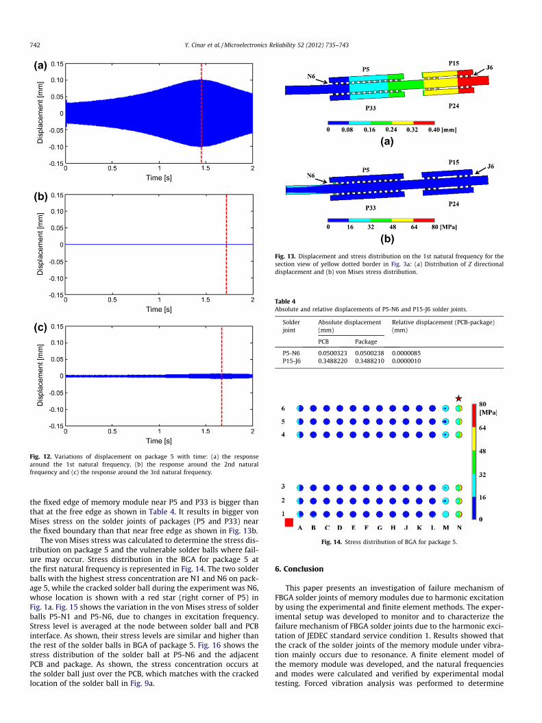
Fig. 12. Variations of displacement on package 5 with time: (a) the responsearound the 1st natural frequency, (b) the response around the 2nd naturalfrequency and (c) the response around the 3rd natural frequency.
Fig. 13. Displacement and stress distribution on the 1st natural frequency for thesection view of yellow dotted border in Fig. 3a: (a) Distribution of Z directionaldisplacement and (b) von Mises stress distribution.
Table 4Absolute and relative displacements of P5-N6 and P15-J6 solder joints.
Solderjoint
Absolute displacement(mm)
Relative displacement (PCB-package)(mm)
PCB Package
P5-N6 0.0500323 0.0500238 0.0000085P15-J6 0.3488220 0.3488210 0.0000010
Fig. 14. Stress distribution of BGA for package 5.
742 Y. Cinar et al. / Microelectronics Reliability 52 (2012) 735–743
the fixed edge of memory module near P5 and P33 is bigger thanthat at the free edge as shown in Table 4. It results in bigger vonMises stress on the solder joints of packages (P5 and P33) nearthe fixed boundary than that near free edge as shown in Fig. 13b.
The von Mises stress was calculated to determine the stress dis-tribution on package 5 and the vulnerable solder balls where fail-ure may occur. Stress distribution in the BGA for package 5 atthe first natural frequency is represented in Fig. 14. The two solderballs with the highest stress concentration are N1 and N6 on pack-age 5, while the cracked solder ball during the experiment was N6,whose location is shown with a red star (right corner of P5) inFig. 1a. Fig. 15 shows the variation in the von Mises stress of solderballs P5-N1 and P5-N6, due to changes in excitation frequency.Stress level is averaged at the node between solder ball and PCBinterface. As shown, their stress levels are similar and higher thanthe rest of the solder balls in BGA of package 5. Fig. 16 shows thestress distribution of the solder ball at P5-N6 and the adjacentPCB and package. As shown, the stress concentration occurs atthe solder ball just over the PCB, which matches with the crackedlocation of the solder ball in Fig. 9a.
6. Conclusion
This paper presents an investigation of failure mechanism ofFBGA solder joints of memory modules due to harmonic excitationby using the experimental and finite element methods. The exper-imental setup was developed to monitor and to characterize thefailure mechanism of FBGA solder joints due to the harmonic exci-tation of JEDEC standard service condition 1. Results showed thatthe crack of the solder joints of the memory module under vibra-tion mainly occurs due to resonance. A finite element model ofthe memory module was developed, and the natural frequenciesand modes were calculated and verified by experimental modaltesting. Forced vibration analysis was performed to determine
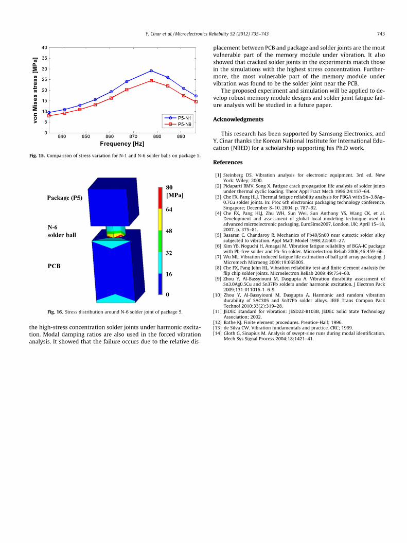
Fig. 15. Comparison of stress variation for N-1 and N-6 solder balls on package 5.
Fig. 16. Stress distribution around N-6 solder joint of package 5.
Y. Cinar et al. / Microelectronics Reliability 52 (2012) 735–743 743
the high-stress concentration solder joints under harmonic excita-tion. Modal damping ratios are also used in the forced vibrationanalysis. It showed that the failure occurs due to the relative dis-
placement between PCB and package and solder joints are the mostvulnerable part of the memory module under vibration. It alsoshowed that cracked solder joints in the experiments match thosein the simulations with the highest stress concentration. Further-more, the most vulnerable part of the memory module undervibration was found to be the solder joint near the PCB.
The proposed experiment and simulation will be applied to de-velop robust memory module designs and solder joint fatigue fail-ure analysis will be studied in a future paper.
Acknowledgments
This research has been supported by Samsung Electronics, andY. Cinar thanks the Korean National Institute for International Edu-cation (NIIED) for a scholarship supporting his Ph.D work.
References
[1] Steinberg DS. Vibration analysis for electronic equipment. 3rd ed. NewYork: Wiley; 2000.
[2] Pidaparti RMV, Song X. Fatigue crack propagation life analysis of solder jointsunder thermal cyclic loading. Theor Appl Fract Mech 1996;24:157–64.
[3] Che FX, Pang HLJ. Thermal fatigue reliability analysis for PBGA with Sn–3.8Ag–0.7Cu solder joints. In: Proc 6th electronics packaging technology conference,Singapore; December 8–10, 2004. p. 787–92.
[4] Che FX, Pang HLJ, Zhu WH, Sun Wei, Sun Anthony YS, Wang CK, et al.Development and assessment of global–local modeling technique used inadvanced microelectronic packaging, EuroSime2007, London, UK; April 15–18,2007. p. 375–81.
[5] Basaran C, Chandaroy R. Mechanics of Pb40/Sn60 near eutectic solder alloysubjected to vibration. Appl Math Model 1998;22:601–27.
[6] Kim YB, Noguchi H, Amagai M. Vibration fatigue reliability of BGA-IC packagewith Pb-free solder and Pb–Sn solder. Microelectron Reliab 2006;46:459–66.
[7] Wu ML. Vibration induced fatigue life estimation of ball grid array packaging. JMicromech Microeng 2009;19:065005.
[8] Che FX, Pang John HL. Vibration reliability test and finite element analysis forflip chip solder joints. Microelectron Reliab 2009;49:754–60.
[9] Zhou Y, Al-Bassyiouni M, Dasgupta A. Vibration durability assessment ofSn3.0Ag0.5Cu and Sn37Pb solders under harmonic excitation. J Electron Pack2009;131:011016-1–6-9.
[10] Zhou Y, Al-Bassyiouni M, Dasgupta A. Harmonic and random vibrationdurability of SAC305 and Sn37Pb solder alloys. IEEE Trans Compon PackTechnol 2010;33(2):319–28.
[11] JEDEC standard for vibration: JESD22-B103B, JEDEC Solid State TechnologyAssociation; 2002.
[12] Bathe KJ. Finite element procedures. Prentice-Hall; 1996.[13] de Silva CW. Vibration fundamentals and practice. CRC; 1999.[14] Gloth G, Sinapius M. Analysis of swept-sine runs during modal identification.
Mech Sys Signal Process 2004;18:1421–41.