new developments in satcom amplifiers and antennas
TRANSCRIPT

New Developments in SATCOM Amplifiers and Antennas
March 2019
S P O N S O R E D B Y
eBook

Table of Contents
2
3 Introduction Pat Hindle Microwave Journal Editor
10 Antenna Technologies for the Future Patrick Hindle Microwave Journal Editor
Strong Defense Outlook Offers Continued Growth for 4 RF Technologies Asif Anwar Strategy Analytics, Newton, Mass.
8 Ultra-Cool GaN on Diamond Power Amplifiers for SATCOM Felix Ejeckam, Ty Mitchell, Kris Kong and Paul Saunier Akash Systems Inc., San Francisco, Calif.
17 GaN SSPA Technology for Space-Based Applications Mario LaMarche Mercury Systems, San Jose, Calif.

3
Introduction
Pat Hindle, Microwave Journal Editor
New Developments in SATCOM Amplifiers and Antennas
Satellite Communications’ (SATCOM) systems are undergoing several changes in technology with a move to higher frequencies and wider bandwidths in traditional design approaches. New technologies are coming into play such as GaN amplifiers that greatly improve SWaP plus offer efficiency and reliability improvements. Different antenna technologies are also greatly impacting the design of systems including phased arrays, metamaterials and 3D printed antennas. The launch of 5G and IoT services is also affecting the SATCOM market as companies are finding ways to utilize their constellations for these markets as opportunities for commercial growth. The growth of the new space market is also affecting design that needs to be low in cost and have a much smaller size and lighter weight, especially for small satellites.
This eBook covers new RF design techniques being used in the area of SATCOM. It starts off with an overview of defense technologies by Strategy Analytics to provide a context of the trends in military RF technologies including SATCOM. According to Strategy Analytics, communicating voice, data and video simultaneously and securely over wider and higher bandwidths in an increasingly complex spectrum environment will underpin the trends in military communications system design and supporting components, including software-defined architectures, solid-state technologies such as GaN, radio-satellite communications and integration with wireless networks. Strategy Analytics forecasts spending on global military communications systems and services will grow to over $36.7 billion in 2026, a compound annual growth rate of 3.5 percent.
There are two articles on the design of GaN amplifiers for SATCOM including new GaN-on-diamond amplifiers and another on space qualified GaN amplifiers. These articles show the significant improvement in amplifier performance over existing solid state devices and TWT devices. There are major improvements in SWaP plus reliability and efficiency gains making these technologies valuable for future applications in SATCOM.
Another article takes a look at new antenna technologies that promise great improvements for SATCOM and other applications. This article includes a review of several companies using innovative technologies like 3D printing, metamaterials, fractal shapes to manufacture new types of antenna structures. These technologies are improving SWaP for SATCOM, 5G, IoT and radar.
This eBook highlights some of the exciting new developments in SATCOM RF design from amplifier to antenna technologies that are improving the performance of devices and system. It is sponsored by Richardson Electronics and Qorvo so want to thank them for supporting this effort.

WWW.MWJOURNAL.COM/ARTICLES/309934
Strong Defense Outlook Offers Continued Growth for RF TechnologiesAsif AnwarStrategy Analytics, Newton, Mass.
The defense sector has been a technology incubator for RF technologies for decades. This article explores the latest market forecasts from Strategy Analytics and how spending on military systems will dictate demand for RF technologies such as GaN.
Strategy Analytics forecasts global defense spending will continue to grow, driven by force modernization requirements and political intent
in the U.S., Western European and other advanced na-tions. A need to counter both resurging conventional threats from near-peers, coupled with ongoing asym-metric wars against non-state or pseudo-state actors, will drive military equipment and capability and support procurement opportunities for the defense industry supply chain to a forecast of $827 billion, part of the projected $2.58 trillion global defense budget in 2027 (see Figure 1).
The U.S. will remain the largest defense market in the world. Strategy Analytics’ model forecasts U.S.
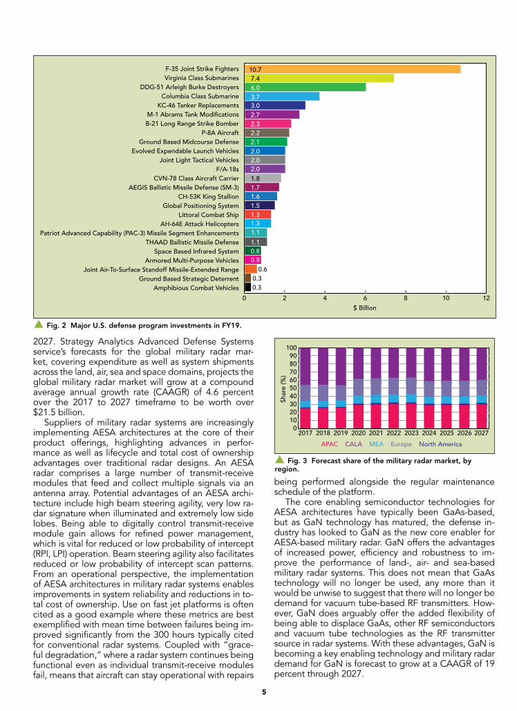
defense spending will grow to $866.6 billion in 2026. The emphasis by the Trump administration to renew U.S. leadership across the world was reflected in the fiscal year (FY) 2018 budget and has been further ce-mented by the most recent FY 2019 budget request: $686 billion for the U.S. DoD with a number of major warfighting investments across airborne, naval, ground and space platforms and systems (see Figure 2). This will maintain momentum behind the U.S. defense in-dustry, sustaining growth for major suppliers like Boe-ing, General Dynamics, Lockheed Martin and Raytheon, as well as the enabling technology supply chain epito-mized by companies such as Microsemi, Qorvo, Tele-dyne and Wolfspeed.
Globally, an emphasis on improved capabilities at the system level will drive demand for military radar, mili-tary communications and electronic warfare (EW), and capabilities will con-tinue to provide opportunities for en-abling technologies such as GaN.
RADARActive electronically scanned array
(AESA) architectures enabled using GaN and GaAs semiconductor tech-nologies will continue to underpin radar systems and serve to catalyze military radar market growth through s Fig. 1 Global defense spending outlook, by region.
5-Year SIPRI Figure1,000
900800700600500400300200100
02013 2014 2015 2016
$ B
illio
n
APAC CALA MEA Europe North America
2017 2018 2019 2020 2021 2022 2023 2024 2025 2026 2027
10-Year Strategic Analytics Forecast
5
2027. Strategy Analytics Advanced Defense Systems service’s forecasts for the global military radar mar-ket, covering expenditure as well as system shipments across the land, air, sea and space domains, projects the global military radar market will grow at a compound average annual growth rate (CAAGR) of 4.6 percent over the 2017 to 2027 timeframe to be worth over $21.5 billion.
Suppliers of military radar systems are increasingly implementing AESA architectures at the core of their product offerings, highlighting advances in perfor-mance as well as lifecycle and total cost of ownership advantages over traditional radar designs. An AESA radar comprises a large number of transmit-receive modules that feed and collect multiple signals via an antenna array. Potential advantages of an AESA archi-tecture include high beam steering agility, very low ra-dar signature when illuminated and extremely low side lobes. Being able to digitally control transmit-receive module gain allows for refined power management, which is vital for reduced or low probability of intercept (RPI, LPI) operation. Beam steering agility also facilitates reduced or low probability of intercept scan patterns. From an operational perspective, the implementation of AESA architectures in military radar systems enables improvements in system reliability and reductions in to-tal cost of ownership. Use on fast jet platforms is often cited as a good example where these metrics are best exemplified with mean time between failures being im-proved significantly from the 300 hours typically cited for conventional radar systems. Coupled with “grace-ful degradation,” where a radar system continues being functional even as individual transmit-receive modules fail, means that aircraft can stay operational with repairs
being performed alongside the regular maintenance schedule of the platform.
The core enabling semiconductor technologies for AESA architectures have typically been GaAs-based, but as GaN technology has matured, the defense in-dustry has looked to GaN as the new core enabler for AESA-based military radar. GaN offers the advantages of increased power, efficiency and robustness to im-prove the performance of land-, air- and sea-based military radar systems. This does not mean that GaAs technology will no longer be used, any more than it would be unwise to suggest that there will no longer be demand for vacuum tube-based RF transmitters. How-ever, GaN does arguably offer the added flexibility of being able to displace GaAs, other RF semiconductors and vacuum tube technologies as the RF transmitter source in radar systems. With these advantages, GaN is becoming a key enabling technology and military radar demand for GaN is forecast to grow at a CAAGR of 19 percent through 2027.
s Fig. 2 Major U.S. defense program investments in FY19.
$ Billion
0 2 4 6 8 10 12
F-35 Joint Strike FightersVirginia Class Submarines
DDG-51 Arleigh Burke DestroyersColumbia Class Submarine
KC-46 Tanker ReplacementsM-1 Abrams Tank Modi�cationsB-21 Long Range Strike Bomber
P-8A AircraftGround Based Midcourse Defense
Evolved Expendable Launch VehiclesJoint Light Tactical Vehicles
F/A-18sCVN-78 Class Aircraft Carrier
AEGIS Ballistic Missile Defense (SM-3)CH-53K King Stallion
Global Positioning SystemLittoral Combat Ship
AH-64E Attack HelicoptersPatriot Advanced Capability (PAC-3) Missile Segment Enhancements
THAAD Ballistic Missile DefenseSpace Based Infrared System
Armored Multi-Purpose VehiclesJoint Air-To-Surface Standoff Missile-Extended Range
Ground Based Strategic DeterrentAmphibious Combat Vehicles
1.31.31.1
1.10.80.8
0.30.3
0.6
7.46.03.7
2.22.32.73.0
1.82.02.02.02.1
1.51.61.7
10.7
s Fig. 3 Forecast share of the military radar market, by region.
1009080706050403020100
Shar
e (%
)
APAC CALA MEA Europe North America
2017 2018 2019 2020 2021 2022 2023 2024 2025 2026 2027

6
Strategy Analytics also predicts:• North America will continue to represent the largest
regional end market, but the fastest growth will come from demand in the Asia-Pacific region (see Figure 3).
• Airborne radar will represent the largest market, both in dollars and total shipments.
• Early warning, surveillance and fire control radars will account for around 76 percent of the global military radar market.
• L-, S- and C-Band will represent the largest market, followed by radars operating at X-Band, which reflect the primary frequencies used by surveillance, early warning and fire control radars.
• The total number of radar shipments is forecast to grow at a CAAGR of 4.6 percent through 2027 to reach 1,607 units. Fire control radar and early warn-ing and surveillance radar shipments will account for 48 percent of 2027 military radar shipments.
• The associated market for semiconductors and other components will grow from $2 billion in 2017 to reach $5 billion in 2027.
EWOperational requirements to establish freedom of ac-
tion in contested and congested environments, as well as the ability to counter modern agile radar and com-munications will drive opportunities for the EW market. There is a renewed push to upgrade conventional EW capabilities that support anti-access/anti-denial (AA/AD) strategies. This will be coupled with the ongoing requirement to combat asymmetric threat scenarios. Future systems will employ wideband solid-state semi-conductors to enable artificial intelligence (AI)-based machine learning algorithms to provide cognitive analy-
sis of the threat environment. EW will play an important role in tackling the increasing complexity that comes with operating in a spectrally constrained environment.
Companies providing systems and enabling technol-ogies will need to focus on solutions that employ wide-band materials, such as GaN, and AESA architectures to enable machine learning-based cognitive analysis, planning and countermeasures activity that can either augment or circumvent the traditional threat library.
Strategy Analytics forecasts the global EW market will grow to $20 billion by 2027 (see Figure 4). The associ-ated market for semiconductors and other components for RF-based EW systems will grow at a CAAGR of 8.4 percent through 2027. Future EW program will increas-ingly use GaN, making this semiconductor technology a staple ingredient in EW systems. This will be coupled with requirements for direct and faster digital synthesis of RF signals across the full frequency spectrum.
COMMUNICATIONSMilitary communications operate under an umbrella
of heterogeneous networks that enable the provision of interoperable voice, video and data services across a global environment, segmented according to security policies, transmission requirements and the individual needs of the end user. In terms of the networked bat-tlespace, this can be summarized as:• Upper level networking, consisting of infrastructure
and networking components.• Mid-level networking providing high capacity back-
haul.• Support to the tactical edge for end-users and sensors.
Similarly, 5G serves as an aggregator technology that encompasses a range of network types and technolo-gies to serve traditional voice, video and data require-ments to the end user, as well as enabling capabilities for connectivity across devices, including vehicles, ma-chines, sensors and devices.
Phased arrays, beamforming, mmWave frequencies, SATCOM, GaN, duplex communications and shared spectrum access are among the crossover technologies that will become common across both commercial and military communications.
Communicating voice, data and video simultane-ously and securely over wider and higher bandwidths in an increasingly complex spectrum environment will underpin the trends in military communications system design and supporting components, including software-defined architectures, solid-state technologies such as GaN, radio-satellite communications and integration with wireless networks.
Strategy Analytics forecasts spending on global mili-tary communications systems and services will grow to over $36.7 billion in 2026, a compound annual growth rate of 3.5 percent (see Figure 5).
RF GaN GROWTHDemand from military radar, EW and communications
applications will provide the primary drivers for GaN market adoption, and this will be coupled with ongoing demand from the rollout of commercial wireless infra-
s Fig. 4 Global EW market forecast.
25
20
15
10
5
0
$ B
illio
n
2017 2018 2019 2020 2021 2022 2023 2024 2025 2026 2027
s Fig. 5 Global military communications market outlook, by segment.
40
35
30
25
20
15
10
5
0
$ B
illio
n
Radio SATCOM Datalink Network Other
2017 2018 2019 2020 2021 2022 2023 2024 2025 20262016
7
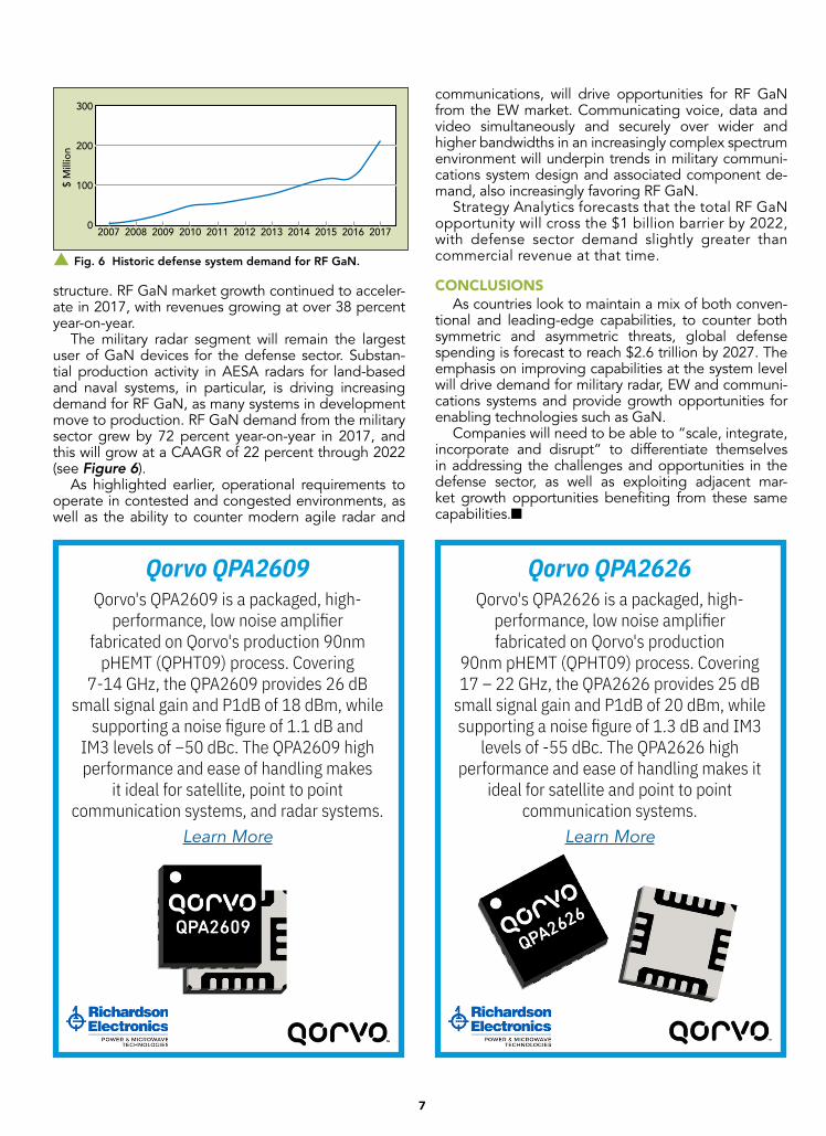
structure. RF GaN market growth continued to acceler-ate in 2017, with revenues growing at over 38 percent year-on-year.
The military radar segment will remain the largest user of GaN devices for the defense sector. Substan-tial production activity in AESA radars for land-based and naval systems, in particular, is driving increasing demand for RF GaN, as many systems in development move to production. RF GaN demand from the military sector grew by 72 percent year-on-year in 2017, and this will grow at a CAAGR of 22 percent through 2022 (see Figure 6).
As highlighted earlier, operational requirements to operate in contested and congested environments, as well as the ability to counter modern agile radar and
communications, will drive opportunities for RF GaN from the EW market. Communicating voice, data and video simultaneously and securely over wider and higher bandwidths in an increasingly complex spectrum environment will underpin trends in military communi-cations system design and associated component de-mand, also increasingly favoring RF GaN.
Strategy Analytics forecasts that the total RF GaN opportunity will cross the $1 billion barrier by 2022, with defense sector demand slightly greater than commercial revenue at that time.
CONCLUSIONSAs countries look to maintain a mix of both conven-
tional and leading-edge capabilities, to counter both symmetric and asymmetric threats, global defense spending is forecast to reach $2.6 trillion by 2027. The emphasis on improving capabilities at the system level will drive demand for military radar, EW and communi-cations systems and provide growth opportunities for enabling technologies such as GaN.
Companies will need to be able to “scale, integrate, incorporate and disrupt” to differentiate themselves in addressing the challenges and opportunities in the defense sector, as well as exploiting adjacent mar-ket growth opportunities benefiting from these same capabilities.n
s Fig. 6 Historic defense system demand for RF GaN.
300
200
100
0
$ M
illio
n
2008 2009 2010 2011 2012 2013 2014 2015 20162007 2017
Qorvo QPA2626Qorvo's QPA2626 is a packaged, high-
performance, low noise amplifier fabricated on Qorvo's production
90nm pHEMT (QPHT09) process. Covering 17 – 22 GHz, the QPA2626 provides 25 dB
small signal gain and P1dB of 20 dBm, while supporting a noise figure of 1.3 dB and IM3
levels of -55 dBc. The QPA2626 high performance and ease of handling makes it
ideal for satellite and point to point communication systems.
Learn More
Qorvo QPA2609Qorvo's QPA2609 is a packaged, high-
performance, low noise amplifier fabricated on Qorvo's production 90nm
pHEMT (QPHT09) process. Covering 7-14 GHz, the QPA2609 provides 26 dB
small signal gain and P1dB of 18 dBm, while supporting a noise figure of 1.1 dB and
IM3 levels of −50 dBc. The QPA2609 high performance and ease of handling makes
it ideal for satellite, point to point communication systems, and radar systems.
Learn More

T he most advanced commercial satellites trans-mit data down to Earth at rates of 100 to 200 Mbps; some advanced larger single satellite concepts target 1 to 4 Gbps. These data rates
are substantially limited by state-of-the-art RF power amplifiers used to make the transmitters. Akash is build-ing, for the first time, a small satellite system (12U) that will exhibit a preliminary downlink data rate of 14 Gbps. The next demo will feature data rates of over 100 Gbps. The ultimate technical goal is to demonstrate a down-link data rate of 1 Tbps from a single, modest size satel-lite—using GaN on Diamond RF power amplifiers.
Ultra-Cool GaN on Diamond Power Amplifiers for SATCOMFelix Ejeckam, Ty Mitchell, Kris Kong and Paul SaunierAkash Systems Inc., San Francisco, Calif.
GAN ON DIAMONDFelix Ejeckam, co-founder of Akash Systems Inc.,
invented GaN on Diamond in 20031 as a way to ex-tract heat effectively from the hottest locations in a GaN transistor. The basic concept is that a cooler GaN amplifier would make the system more energy efficient, and less wasteful. On a GaN on Diamond wafer, the GaN channel or epitaxy is extracted from its original substrate of Si and situated on a CVD dia-mond substrate via a 35 nm SiN interfacial layer. This nanometer-scale proximity of a 200°C GaN channel to CVD diamond, the most thermally conductive indus-
trial material, drastically reduces the thermal rise between the amplifier’s base plate and the channel tempera-ture. Figure 1 shows the process of making GaN on Diamond wafers and devices. Many parties over the years have quantified the aforementioned thermal improvement.2 A GaN on Si HEMT wafer is bonded to a tem-porary Si carrier. The original Si sub-strate is etched away, followed by CVD deposition of diamond via a 35 nm interfacial layer below the GaN. Finally, the temporary Si carrier is etched away. The eventual GaN on Diamond wafer is then processed into an array of HEMTs or MMICs.
s Fig. 1 GaN on Diamond wafer process.
TempCarrier
Substrate
GaN HEMT
Diamond
GaN HEMT
TempCarrier
GaN HEMT
ConventionalGaN on Si
WaferBonding
DirectDiamond
DepositionTemp Carrier
RemovalReady For
HEMTs
TempCarrier
Substrate
GaN HEMT
TempCarrier
Diamond
GaN HEMT
GaN Buffer
Adhesive (10 nm)
WWW.MWJOURNAL.COM/ARTICLES/304518

9
SYSTEM IMPACTIf the thermal rise of a GaN MMIC can be shrunk by
40 to 50 percent compared to GaN on SiC, then greater power density can be squeezed into a smaller volumetric space.3 Power is a direct parameter in a satellite’s down-link data-rate budget calculation; more information can be transmitted if there is more power. Cooling require-ments in a very compact space are relaxed with GaN on Diamond since the ambient temperature can be allowed
to rise higher than with a typical GaN on SiC power am-plifier system—without compromising performance or reliability. This reduction in cooling gear also means less weight and size, both key parameters in the cost of launching a satellite system into orbit.
PERFORMANCEAkash designers have recently demonstrat-
ed high performing GaN on Diamond tran-sistors (i.e., simplified power amplifiers) at K-Band exhibiting 60 percent power added efficiency (PAE) at 20 GHz (see Figure 2). In another recent work, funded by DARPA and performed by a team of re-searchers at Georgia Tech, Stanford, UCLA and Element Six, the GaN device’s thermal rise—change in tempera-ture from the GaN channel to the substrate bottom—was found to reduce by 80°C when compared to the same device on GaN on SiC.2 The wafer used in the work is identical to the GaN on Diamond process used by Akash Systems.
Figure 3 shows the temperature distribution for the channels from the center to the edge of the 10 finger HEMT for various types of GaN on Diamond wafers. Akash Systems uses the “Gradient Diamond with Low Thermal Boundary Resistance (TBR)” process GaN on Diamond wafers (in green); this curve registers 152°C peak temperature (the first peak). GaN on SiC registers 232°C at the same point on the device.2
Akash Systems is planning to launch into a LEO orbit in 2019, a 24 kg 12U (36 cm x 24 cm x 23 cm) satellite system that will contain a 20 W transmitter radio built on a GaN on Diamond power amplifier. The system will exhibit a land-mark 14 Gbps data rate unique for a system that size.n
References1. F. Ejeckam, D. Francis, F. Faili, D.J. Twitchen, B. Bolliger, J. Felbin-
ger and D. Babic, “S2-T1: GaN on Diamond: A Brief History,” Les-ter Eastman Conference on High Performance Devices, August 5–7 2014, DOI: 10.1109/LEC.2014.6951556. INSPEC Accession Number: 14775316.
2. L. Yates, A. Sood, Z. Cheng, T. Bougher, K. Malcom, J. Cho, M. Asheghi, K. Goodson, M. Goorsky, F. Faili, D.J. Twitchen and S. Graham, “Characterization of the Thermal Conductivity of CVD Diamond for GaN on Diamond Devices,” Compound Semicon-ductor Integrated Circuit Symposium (CSICS) 2016 IEEE, pp. 1–4.
3. G.D. Via, J.G. Felbinger, J. Blevins, K. Chabak, G. Jessen, J. Gil-lespie, R. Fitch, A. Crespo, K. Sutherlin, B. Poling, S. Tetlak, R. Gilbert, T. Cooper, R. Baranyai, J.W. Pomeroy, M. Kuball, J.J. Mau-rer and A. Bar-Cohen, “Wafer-Scale GaN HEMT Performance En-hancement by Diamond Substrate Integration,” 10th International Conference on Nitride Semiconductors, August 25-30, 2013, Washington, D.C.
s Fig. 2 Example device shows 61 percent PAE from a 2.9 W (5.6 W/mm) HEMT with 7.9 dB gain. Bias point is 24 V.
35
30
25
20
15
10
5
0
70
60
50
40
30
20
10
0–5 0 5 10
Po
wer A
dd
ed E
f�ciency (%)
Out
put
Po
wer
(dB
m) G
ain
(dB
)
Input Power (dBm)
15 20 25 30
20 GHz: 2.9 W (5.6 W/mm) with 7.9 dB Gainand 60.5% Ef�ciency at Vd=24 V
Output Power
Gain
PAE
s Fig. 3 Graph showing the temperature distribution for the channels from the center to the edge of the 10 finger HEMT for various types of GaN on Diamond wafers.
170
160
150
140
130
120
110
1001000 200 350 400
Tem
per
atur
e (°
C)
Position from Device Center (µm)
Gradient Dia with High TBRNo Gradient Dia with High TBR
Gradient Dia with Low TBRNo Gradient Dia with Low TBR

10
Traditional antenna technology has hit its lim-its in many demanding commercial and aero-space markets such as 5G, SATCOM, IoT and radar. But there are many companies develop-
ing new approaches and materials that could drastically improve antenna performance and enable new applica-tions that were not previously envisioned because of these limitations. In this article, Microwave Journal looks at a sampling of these technologies that have come to our attention in the last couple of years.
3D PRINTED ANTENNASRecent advances in 3D printing or additive manu-
facturing have enabled complex RF structures to be realized. The characterization of the materials used in 3D printing processes has been shown to be critical in designing and accurately predicting the performance of these structures. Understanding the RF properties of the materials through characterization has led to the development of novel structures that could not ever be realized with traditional manufacturing techniques. 3D printing has also allowed manufacturers to produce tra-ditional antenna shapes with less weight and at a lower cost.
SWISSto12 SA is an offshoot from the Swiss Fed-eral Institute of Technology in Lausanne, Switzerland. The company has developed unique products using 3D printing that are based on polymer materials that are then metal plated or on metallic materials (such as alu-minum or titanium) combined with advanced surface
Antenna Technologies for the Future Patrick HindleMicrowave Journal Editor
treatments and surface plating. Using these processes, SWISSto12 manufactures and tests aerospace quali-fied advanced RF products such as waveguides, filters, beamforming networks, antenna feed chains or array antennas.
Their use of 3D printing allows for increased flexibil-ity in the manufacturing of complex product designs. This freedom can be used to produce higher complexity RF components, which often allows for better RF per-formance. Traditional machining technologies used to manufacture RF products are limited in their ability to produce products with complex shapes. To circumvent this limitation, complex products are often assembled out of a larger number of simpler sub-components that are produced separately. SWISSto12’s 3D printing tech-nology does not have such constraints, allowing it to produce entire products in one single element that posi-tively impact mass, cost, lead time, assembly quality and RF performance. The use of 3D printing also allows for optimized weight reduction. The technology has been demonstrated on waveguide, filter and antenna compo-nents from C- to W-Band (4 to 110 GHz).
As this technology is rapidly gaining maturity and ac-ceptance among the aerospace industry, SWISSto12 has already delivered a variety of prototypes to organizations in the space and SATCOM industries that have been qualified for use in airborne and space environments (the first commercial programs will be flying SWISS-to12 products in 2018). More complex and integrated antenna or payload structures are in development, in
WWW.MWJOURNAL.COM/ARTICLES/29572

11
particular Ku- and Ka-Band products. The company is also targeting emerging market opportunities such as high-altitude platforms, UAVs and Cubesat constella-tions. An example antenna product is a Ku-Band dual-reflector antenna comprising a conical chocked horn, a sub-reflector, a main reflector and metallic supports. This antenna system only weighs 145 g. The radiation properties of this antenna were found to be in an excel-lent agreement with simulation results over the design frequency range (see Figure 1). This antenna demon-strator was manufactured and tested in collaboration with the European Space Agency.
Optisys is another company that focuses on the de-sign, fabrication and test of lightweight antennas using metal 3D printing. The specific method that Optisys uses for fabrication is a powder bed fusion process, where thin layers of powder are welded into solid metal by a high-power laser. Through this welding process, a part is built one small layer at a time. This green manu-facturing process allows for material to be added only where absolutely necessary to achieve a given mechani-cal or RF function.
As with any fabrication process, 3D printing has a set of design rules that determines what can and cannot be included in a design. Optisys is reimagining how wave-guide is routed to achieve a desired RF function to take full advantage of the strengths of the printing process that allows, in some cases, for over an order-of-magnitude re-duction in the size and weight of an antenna. Along with size and weight, part count reductions and absorbing tol-erance stack-up can lead to simpler antenna assemblies with improved performance.
Optisys has designed a number of arrays using build-ing blocks developed in-house that are rearranged and optimized for different functions and frequency bands. One of the key antenna designs is a Ka-Band 16-ele-ment tracking array shown in Figure 2. Signal patterns show the sum and delta elevation performance with measured and simulated performance overlaid. This
s Fig. 1 Swissto12 Ku-Band dual-reflector antenna (a) image courtesy of the ESA, and the radiation properties over the design frequency range (b).
0
–10
–20
–30
–40
–50
–60806040200–20–40–60–80
(dB
)
Angle from Boresight (°)
14.5 GHz
(a)
(b)
Co-Polar MeasurementsCx-Polar Measurements
Co-Polar MoM SimulationsCx-Polar MoM Simulations
s Fig. 2 Optisys Ka-Band 16-element tracking array with measured and simulated data.
0
–5.00
–10.00
–15.00
–20.00
–25.00
–30.00
–35.00
–40.006040200–20–40–60
Nor
mal
ized
Gai
n (d
B)
Elevation Normalized Gain 31.0 GHz
Elevation Angle (°)
Simulated Sum Simulated Delta ElMeasured Sum Measured Delta El
s Fig. 3 Optisys Ka-Band 64-element tracking array with signal pattern.

12
a dielectric support. This design has been optimized to the key frequency bands of X-, Ku- and Ka-Band. The company refers to these antenna feeds as the integrat-ed printed antenna family of feeds. The unit and 3D near-field scan pattern at a single frequency and a set of elevation patterns across the frequency band are shown in Figure 4.
As covered in the October 2016 issue of Microwave Journal, The MITRE Corporation is investigating a new generation of 3D printing to realize the complex ge-ometries of wideband phased array and metamaterial designs using commercial, low-cost, compact, desktop printers.1 Samples of the 3D printed plastic and conduc-tive ink printed at room temperature were characterized over frequency. The polylactic acid (PLA) dielectric con-stant and loss tangent are found to be stable up to 18 GHz. The PLA internal architecture was varied to achieve lower effective dissipation factors, which extends use-fulness to high frequency applications. Microstrip line samples were fabricated with simulated and measured insertion loss data validating the high conductivity through mmWave frequencies. A 3D printed monopole Wi-Fi antenna was built and tested, showing good per-formance and agreement with simulations.
MITRE also has developed a wideband phased array concept that has a complex metamaterial design. It is based on a PCB design that was not physically realizable with traditional manufacturing. The design resembles an egg-crate construction with contiguous electrical con-nection (interdigitiated fingers) that is embedded within the orthogonal board interface, as illustrated in Figure 5.1 Multi-material additive manufacturing is thought to be the only practical way to realize this design. They suc-cessfully printed a sample of the cross in the middle of the array, and a CT-scan showed the details of all of the fingers confirming the construction and working on full scale antenna structures.
METAMATERIAL BASED ANTENNASMetamaterials are made by arranging naturally oc-
curring materials in a specific pattern that produces an electromagnetic response that is not found in nature. The periodic structures created are at scales that are smaller than the wavelengths of the phenomena they influence and can create materials with negative indexes that control electromagnetic energy in ways that cannot be done with natural materials. In traditional active electroni-cally scanned arrays (AESA), phase shifters embedded in control circuitry steer the beam direction. Metamaterial-based AESAs can steer the beam without phase shifters,
part includes a 16-ele-ment array of horns that are circularly polarized, with a waveguide com-biner network on both left- and right-hand circular polarizations. Additionally, the right- hand combiner network feeds into a dual-axis monopulse compara-tor. All of this is imple-mented in a single part that weighs less than 2 oz and fits in the palm of the hand.
A second array design is the X64 antenna that takes the integration a step further, by including a waveguide dual-axis monopulse comparator on both polarizations and in-tegrating an elevation rotation axis into the design. Fabri-cating this part in a traditional process would require well over 100 separate parts, compared to the single printed part. Signal patterns are shown for sum, delta elevation and delta azimuth on the right-hand circular polarization (see Figure 3). There are a total of eight simultaneous an-tenna beams generated in this antenna.
Another key area of innovation where Optisys has generated interest is in the design and building of light-weight feeds for parabolic reflectors, where the sub-re-flector, feed horn and polarizer are printed as a single metal part without blockage or losses due to struts or
s Fig. 4 Optisys Integrated Printed Antenna and signal pattern.
3020100
–10–20–30–40
6060
4040
2020
00
–20–20–40–40
–60–60
Elevation (°)Azimuth (°)
Far-
Fiel
d G
ain
(dB
i)
s Fig. 5 A small test coupon of MITRE’s biaxial metamaterial created with a Voxel8 multi-material 3D printer.
s Fig. 6 Kymeta mTenna™ construction.
Backshell(Enclosure)
ControlElectronics
FeedAssembly
TFTAperture
RadomeAssembly Bezel

13
implement satellite technology broadly across smaller vessels and aircraft.
A second company, Echodyne, has developed meta-material arrays for radar using similar antenna technol-ogy to Kymeta but optimized for radar applications. Echodyne’s radar vision platform represents a unique sensor technology that combines the all-weather, long range and ground-truth measurements of radar with high resolution imaging capabilities (see Figure 7).4 Radar vision consists of high performance agile imag-ing radar hardware combined with computer vision-like software for classification, recognition and perception.
Their metamaterial based, electronically steered array radars operate in the same way as traditional designs, providing high resolution data at any time and in any weather. Like Kymeta’s approach, they can be produced in high volume, at commercial price points and in small lightweight form factors. Their technology can switch in less than 1 μs, has beam shaping and multi-beam capa-bilities and can steer in both directions, providing near full hemisphere coverage. It operates at 24 GHz and has an operational range of 3.4 km with a field of view ≥120 degrees azimuth and 80 degrees elelvation with a range resolution of 3.25 m and velocity resolution 0.9 m/s.4
LiDAR and cameras have limited range and do not operate reliably in adverse weather, while traditional ra-dar in this sector has inadequate resolution. Echodyne’s radar vision platform represents a new category of sen-sor technology to enable many autonomous vehicles from drones to cars. Their high performance imaging radar is viable and affordable on commercial and small platforms, including all types of autonomous and un-manned vehicles and machines.
FRACTAL BASED ANTENNASA fractal is “self similar” complex pattern built from
the repetition of a simple shape. A fractal element an-tenna is shaped using fractal geometry. The inherent properties of fractals can enable high performance an-tennas that can be 50 to 75 percent smaller than tradi-tional antennas. Typical advantages are increased band-
which reduces system complexity, eliminates a source of power loss and simplifies waste-heat dissipation. There are a couple of companies us-ing unique metamaterial structures developed for this application.
Kymeta experiment-ed with these structures for many years and dis-covered that the meta-
materials could be used to form holographic beams that could link to satellites and maintain the link while the antenna is in motion. Kymeta mTenna™ technology (see Figure 6) is manufactured using a completely dif-ferent process and components than both traditional antennas and phased array antennas.2 The “metamate-rial” in mTenna technology is a metasurface in a glass structure. Their glass-on-glass structure is manufactured on the same production lines as LCD flat screen televi-sions, making it suited for low-cost, high volume manu-facturing. They use the thin film transistor liquid crystal as a tunable dielectric. Instead of reflecting microwaves like a traditional dish antenna or creating thousands of separate signals like a phased array, Kymeta uses a thin structure with tunable metamaterial elements to create a holographic beam that can transmit and receive satel-lite signals.
They use software to steer the antenna, eliminating the need for mechanical gimbals to point the antenna toward a satellite. The antenna does not require ac-tive phase shifters or amplifiers. Key features of the ap-proach:3
1. Transmit and receive via a single aperture2. Wide angle scanning and excellent beam perfor-
mance3. Electronically controlled pointing and polarization4. Extremely low power consumption5. First electronically scanned antenna
designed for mass production.Traditional satellite dishes are
heavy, large, expensive, consume a lot of power and have mechanical gimbals for steering, which have prevented or limited their adoption on most mobile platforms. Kymeta’s mTenna technol-ogy provides software-enabled, meta-materials-based, electronic beam-forming satellite solutions that are flat, lightweight, small and use software to steer instead of mechanical parts.
This technology is being used to deliver internet connectivity to indus-tries that have historically been inac-cessible or difficult for the satellite in-dustry to address, such as rail, bus and automotive. Also, the maritime and aviation markets have struggled to
s Fig. 7 Echodyne’s radar vision unit next to an iPhone.
s Fig. 8 Fractal Antenna’s RF invisibility cloak and measured data.
151050
–5–10–15–20
151050
–5–10–15–20
500
600
700
800
900
1000
1100
1200
1300
1400
1500
Uncloaked Response
Gai
n (d
B)
Gai
n (d
B)
Cloaked Response
Frequency (MHz)
500
600
700
800
900
1000
1100
1200
1300
1400
1500
Frequency (MHz)

14
nents onto a PCB for low cost assembly (see Figure 9). Aimed at mobile devices and IoT applications, it is made with metalized ceramic layers that use fractal shapes designed to meet different design require-ments.
Miniature chip antennas are not new, so what is unique here is the multiband capability with a single de-vice. While conventional miniature chip antennas were based on high-permittivity ceramics and delivered good performance for narrowband, single frequency applica-tions, these new boosters can deliver full mobile perfor-mance within a broad range of frequency bands (e.g., 698 to 2690 MHz) with a single device. The integration re-quires a matching circuit that allows the device to operate at the desired bands of interest. Based on conventional low-cost materials and assembly processes, the boosters can be made in high volume at very low cost.
An example booster is 5 mm3 in size and operates from 824 to 960 MHz and 1710 to 2170 MHz simultane-ously. With a matching network on the PCB, a VSWR ≤ 3:1 across the operating bands and an average total ef-ficiency of 56.7 and 75.8 percent in the 824 to 960 MHz and 1710 to 2170 MHz frequency regions, respectively, is achieved (see Figure 10).8
OTHER UNIQUE TECHNOLOGIESPlasma Antennas (PSiAn) offers a range of innova-
tive plasma-silicon devices (PSiD) to form the compact RF core of future smart antennas. The PSiDs provide fast, electronic beamforming and beam selection functions. A PSiD can be regarded as a multi-port, wideband switch that replaces RF switches, phase shifters and attenuators with one compact, low loss device. Due to their silicon IC construction, PSiDs can be reproduced with high preci-sion for the mass market at low cost. They have high pow-er handling and, unlike RF MEMS, can be “hot” switched.
PSiAn uses either single or multiple PSiDs to per-form azimuth and elevation beam steering. The PSiDs are mounted on RF PCBs and use transmission lines to link the device ports to traditional RF and antenna technologies, such as LNAs, PAs, printed feeds, lens-es and reflectors to produce efficient smart antennas with steerable narrow beams. Potential applications of PSiAn plasma antennas include: small cell backhaul at V-Band (60 GHz), gigabit wireless LAN (e.g. WiGig), intelligent transport systems (ITS) at 63 GHz and ve-hicle radar (77 GHz).
The company recently introduced an antenna that reduces the cost of a 5G base station by up to 50 per-cent by eliminating phase shifters, reducing and con-solidating amplification and reducing computation. The technology does not need calibration and can handle high-power, having been tested up to 40 W. The com-pany has shown the technology in a variety of scenarios, including a 360 degree field of view, beamforming and steering, 28 GHz, 5 W, 16 dBi gain PSiAN, useful for pole mounted small cells, indoor small cells—also on a vehicle and a high-power, long range, low loss small cell base station antenna for standalone and MIMO 5G, fixed wireless access (FWA) and connected vehicle ap-plications (see Figure 11).9 These devices can also be stacked to form and steer beams in two dimensions
width, better multi-band performance and higher gain. Fractal antennas can be more reliable and lower cost than traditional antennas because antenna performance is attained through the geometry of the conductor, rath-er than with the accumulation of separate components or separate elements that can increase the complexity, potential points of failure and cost.
Fractal Antenna is a small company that produces fractal versions of many existing antenna types, includ-ing dipole, monopole, patch, conformal, biconical, dis-cone, spiral and helical, as well as compact variants of each that is made possible through fractal technology. They were the first to demonstrate wideband RF invis-ibility cloaking and used fractal shaped metal patterns on a mylar sheet. In their demonstration, a signal from 750 to 1250 MHz was attenuated by only a fraction of a dB over the same 50 percent bandwidth that would normally be attenuated by 6 to 15 dB without the cloak (see Figure 8).5,6
At EDI CON USA 2016, Dr. Nathan Cohen of Frac-tal Antenna gave a session and demonstration of their unique RF/microwave cloaking and deflection technol-ogy using fractal structures. Over a broad band, 2.5 to 3 GHz, he created a Waldo (window around a wall) that channeled the RF energy around a barrier (the “wall”) using an array of closely packed fractal-shaped resona-tors that was wrapped around the barrier, creating a “window.” The bandwidth is an impressive 500 percent for front scatter and 100 percent for backscatter with about 1 dB insertion loss.7
Fractus Antennas was featured in the October 2017 issue of Microwave Journal and has a new “an-tenna-less technology” that is based on replacing a
complex and usually customized antenna design with an off-the-shelf, standardized, miniature component called an antenna booster.8 Being a sur-face-mount, chip-like device, the antenna booster can be picked and placed like other surface-mount compo-
s Fig. 9 The CUBE mXTEND™ antenna booster from Fractus Antennas (5 mm3).
s Fig. 10 VSWR and efficiency for 5 band mobile antenna from Fractus Antenna.
6.0
5.0
4.0
3.0
2.0
1.02.101.801.501.200.90
100
80
60
40
20
0
Total Ef�ciency (%
)
VSW
R
Frequency (GHz)
VSWREf�ciency

15
Samsung, for which there are many handling scenarios that would block the antennas. The array Plasma Anten-nas proposes now solves these problems and brings the intrinsic qualities of plasma silicon.
Gapwaves AB was founded in 2011 by Professor Per-Simon Kildal at Chalmers University of Technology in Gothenburg, Sweden, with the aim of enabling ef-ficient wireless communication through the patented GAP waveguide technology. GAP waveguides provide a unique packaging technology for mmWave and terahertz circuits and components, with advantages compared to existing transmission line and waveguide technology. The technology is based on an artificial magnetic conductor that enables contactless propagation of electromagnetic waves, significantly reducing transmission losses. The GAP waveguide is built up of two parts: a structured metal surface and a flat metal surface placed close to one another, allowing for an air gap between the two parts (see Figure 12).11 The structured surface is characterized by pins forming a barrier, preventing the electromagnetic waves from propagating in undesired directions. In this way, the pins replace the walls in traditional rectangular waveguides without requiring perfect metallic contact. The waves are guided by ridges or grooves within the pin struc-ture and propagate in air, resulting in low power losses. Antennas based on the GAP technology have more than 10x lower losses than micro strip lines, more than 3x lower losses than substrate integrated waveguide (SIW) and ap-proximately the same losses as rectangular waveguides.11
As no metallic contact is required between the layers, the assembly of multilayered, closely spaced waveguide structures is simplified. The antenna layers can be glued together with no screws, pressure or heat. Production of the antenna parts is accomplished using plastic injec-tion molding in combination with metallization or using die-casting in metal, resulting in high volume capabili-ties and a cost-efficient manufacturing process. The low power losses enable broadband antenna arrays with gains up to 38 dBi to be achieved with above 80 percent efficiency. The design flexibility that comes from using multilayered waveguide structures enables tailoring of the radiation pattern, as demonstrated by a recently de-veloped 38 dBi E-Band antenna that has achieved ETSI class 3 radiation pattern performance.
The properties of GAP waveguides make it suitable for designing active antenna systems. A schematic view of an active antenna based on the GAP waveguide technology is shown in Figure 13. Due to its contactless nature, GAP waveguide based antennas can be more easily integrated
with PCB, as RF interconnects between the PCB and the antenna layers can be made without electrical contact. The pin structure also acts as a shield for the ac-tive components, protecting them from interference and preventing propaga-tion within the substrate of the PCB. Re-moving the need for shielding walls and via holes frees up valuable circuit board space, which becomes available for the placement of active circuits and routing lines. The die-cast antenna layers also provide effective cooling for the active
(azimuth and elevation) or to form multiple beams and MIMO applications.
They also announced their mmWave PSiAn for use in smartphones and other consumer electronics, delivering high throughput with low latency and utilizing directional beams that generate less interference and maximize en-ergy efficiency.10 The introduction of mmWave connec-tivity for smartphones and other mobile devices faces significant problems as the signals are easily blocked by fingers, hands, heads and bodies. When used in com-bination with distributed radiating elements, PSiDs can be used as a switch and beam former to utilize only ele-ments that are able to receive and transmit line-of-sight or reflected signals resolving this issue. Plasma Antennas recently modeled plasma silicon corner antennas as re-placements for array modules for device manufacturers and silicon suppliers. This approach closely represented the publicly available solutions from Qualcomm and
s Fig. 11 Plasma Antenna 360° field of view beamforming and steering 28 GHz, 5 W, 16 dBi gain PSiAn.
Layer 1
Layer 2
Layer 9
Layer 10
Dig
ital
DSP
s Fig. 12 GAP waveguide structure.
No ElectricalContactBetween
Parts
Structured Metal Surface
Prevent Leakage
FlatmetalSurface
Wav
e
s Fig. 13 Active antenna system construction using GAP waveguide technology.
AntennaFeeding
and Filters
ShieldCover
and CoolingCooling
Plate PCBRadiating
Slots

16
circuits from two sides. This is useful when integrating high-power amplifiers and CMOS based control circuits onto the same circuit board, which often require cooling from differ-ent sides.
SUMMARYThere are many exciting new technologies such as 3D
printing, metamaterials and fractal antennas, that prom-ise to revolutionize antenna technology in the next few years. They will solve many challenges that traditional antenna technology has not been able to overcome and enable new antenna shapes and applications that are not even possible with traditional antenna technology. The unique new approaches will address many of the challenges faced today in 5G, IoT, SATCOM and radar applications.n
References1. M. W. Elsallal, J. Hood and I. McMichael; T. Busbee, “3D Printed
Material Characterization for Complex Phased Arrays and Meta-materials,” Microwave Journal, Vol. 59, No. 10, October 2016.
2. www.kymetacorp.com/kymeta-products/, November 25, 2017.3. www.kymetacorp.com/why-kymeta-connectivity/, November 25,
2017.4. https://echodyne.com/products/, November 26, 2017.5. N. Cohen, “Fractals,” World Scientific Publishing, Vol. 20, Nos. 3
& 4, 2012, pp. 227–232.6. N. Cohen, “Wideband Omnidirectional Microwave Cloaking,”
Microwave Journal, Vol. 15, No. 1, January 2015.7. www.microwavejournal.com/articles/27219, November 20, 2017.8. J. Anguera, A. Andújar and C. Puente, “Antenna-Less Wireless: A
Marriage Between Antenna and Microwave Engineering,” Micro-wave Journal, Vol. 60, No. 10, October 2017.
9. www.microwavejournal.com/articles/29472, November 22, 2017.10. www.microwavejournal.com/articles/29249, November 22, 2017.11. http://blog.gapwaves.com/what-is-a-gap-waveguide, November
26, 2017.
Qorvo QPA2735Qorvo’s QPA2735 is a packaged, high-
performance, low noise amplifier fabricated on Qorvo’s production 90nm
pHEMT (QPHT09) process. Covering 13.75 – 18 GHz, the QPA2735 provides
26 dB small signal gain and P1dB of 18 dBm, while supporting a noise figure of 1.1 dB and
IM3 levels of −58 dBc. The QPA2735 high performance and ease of handling makes
it ideal for satellite and point to point communication systems.
Learn More
Qorvo TGP2105-SMQorvo's TGP2105-SM is a packaged
6-bit digital phase shifter, fabricated on Qorvo's high performance 0.15um GaAs
pHEMT process. It operates over 6 to 18 GHz and provides 360° of phase
coverage with a LSB of 5.625°. It also achieves a low RMS phase error of 4° with
8 dB of insertion loss over all states. TGP2105-SM is ideally suited for a variety
of wideband phased array applications, including commercial and military radars, satellite-based communication systems
and electronic warfare. Learn More

17
Few technology applications are positioned to ben-efit from high-power RF GaN device insertion to the extent as space payloads. Costing roughly
$10,000 per pound of payload to launch a satellite into space, the benefit of small, lightweight hardware is ob-vious. The trend toward low Earth orbit (LEO) satellite constellations is increasing the pressure to develop cost-saving technologies. While GaN is well-positioned to deliver these benefits, its use is not without challenges. To maximize the mean time between failures (MTBF), the thermal conduction path away from the device must be carefully designed. As an added challenge, the lack of industry heritage using GaN in space requires thor-ough analysis and additional qualification testing.
GaN is a III-V direct bandgap semiconductor. Similar to GaAs, its high electron mobility makes it well-suited for RF/microwave applications. Compared to GaAs, the wider bandgap of GaN—3.4 vs. 1.4 eV for GaAs—en-ables operation at very high-power densities. Instead of using bulky combining networks to sum the power of many GaAs devices, a small number of GaN devices will efficiently produce high output power. As GaN technol-ogy continues to mature (see Figure 1), it is replacing some traveling wave tube (TWT) amplifiers, which have been the primary technology for satellite power ampli-fiers for years.
SATELLITE AMPLIFIER TECHNOLOGYAs with nearly all communications systems, satellite
transponders include transmit and receive modules. In the traditional architecture, the uplink signal is passed through a low noise amplifier to a frequency converter, then to the transmit module. Amplifying the signal to the required output level is typically the role of a TWT
GaN SSPA Technology for Space-Based ApplicationsMario LaMarcheMercury Systems, San Jose, Calif.
amplifier. While tube amplifiers produce high-power at Ka-Band, their large size and high-cost are challenging, especially evident with the new generation of LEO satel-lites. Since these satellites must be smaller and less ex-pensive than traditional satellites, relying on expensive and large TWT amplifiers is problematic.
TWTs amplify RF signals through the interaction be-tween an electron beam and the RF signal. While this is an efficient method for generating high output power, TWT amplifiers are inherently complex assemblies, re-quiring the mechanical integration of multiple,
WWW.MWJOURNAL.COM/ARTICLES/31995
s Fig. 1 Increasingly used in radar, EW and communications application, GaN power amplifiers offer size, weight and power benefits for satellites.
18
high-precision components. This complexity drives the high price of TWTs and increases the risk of failure. TWT amplifiers also require very high bias voltage—usu-ally thousands of volts—generated by a high voltage supply, which is also large and expensive. As a rough order-of-magnitude, the size of a Ka-Band TWT ampli-fier with 500 W output power is about 18 in. × 3 in. × 3 in., with an equally large power supply. Not only does the large size of the TWT amplifier restrict its use in LEO satellites, even traditional satellites have strict size and weight limits on their payload systems and will benefit from smaller components.
A solid-state solution offers a more robust, compact option. A GaN power amplifier uses standard IC manu-facturing processes, producing small devices only a few millimeters on each side. Instead of using artisan-style manufacturing, GaN devices are produced using auto-mated semiconductor processes at low-cost. While a single GaN device is unable to deliver the same output power as a TWT amplifier, multiple GaN devices can be combined in a small package. As an added benefit, GaN amplifiers only require bias voltages of 28 to 50 V.
Given the differences between GaN and TWT ampli-fiers, GaN is particularly attractive for applications sensi-tive to size, weight and cost, as well as those that require less transmit power. This precisely describes LEO satel-lites.
CHALLENGES OF GaN IN SPACEWhile GaN amplifiers offer compelling benefits for sat-
ellite applications, specific challenges must be overcome to successfully use GaN in space-qualified hardware. The first and most obvious challenge arises from the high power density of the device. While TWT amplifiers also require a complex cooling system, a GaN IC generates significant heat in a very small space. For example, a 30 W solid-state GaN amplifier can easily draw 2.5 A bi-ased at 28 V, resulting in 40 W power dissipation in an area not much larger than 10 mm2. If the thermal transfer is inadequate to cool the device, the elevated junction temperature will lower output power and reduce MTBF—possibly even causing catastrophic failure.
This raises the second challenge: reliability. The high-power dissipation common with GaN devices results in a significant temperature rise in the active region; as the temperature in the device increases, the reliability of the amplifier degrades. The temperature rise depends on the power dissipation in the GaN and the thermal resis-tance between the device and the case—both difficult to model and control. Power dissipation depends on multiple factors such as RF drive and load impedance, and the thermal resistance is highly dependent on minor variations in the assembly process.
Even under ideal circumstances, where the tem-perature is carefully controlled, high RF drive levels can cause permanent damage to the GaN lattice, resulting in degraded output power. Compared to GaAs, GaN is a much newer technology, and the lack of heritage raises reliability concerns. While this applies to all ap-plications using GaN, operating in a space environment requires an extra focus to assure reliability. Since repair is generally not an option, a single device failure can be
extremely expensive.The design of the GaN ICs and amplifier modules
is also a challenge, especially for space-based applica-tions requiring custom designs for specific programs, rather than using standard, off-the-shelf products. One critical element to first-pass design success is accurate device modeling. Since even class A amplifier design requires nonlinear models, modeling a GaN amplifier is considerably more complex than simply using an S-parameter file.
This discussion highlights several key challenges to implement GaN technology in space-qualified power amplifiers. Addressing these requires multi-disciplinary expertise including, RF design, mechanical design, man-ufacturing and quality. The following sections discuss possible approaches to managing these challenges.
GaN AMPLIFIER THERMAL MANAGEMENTThe high power density in GaN semiconductors pres-
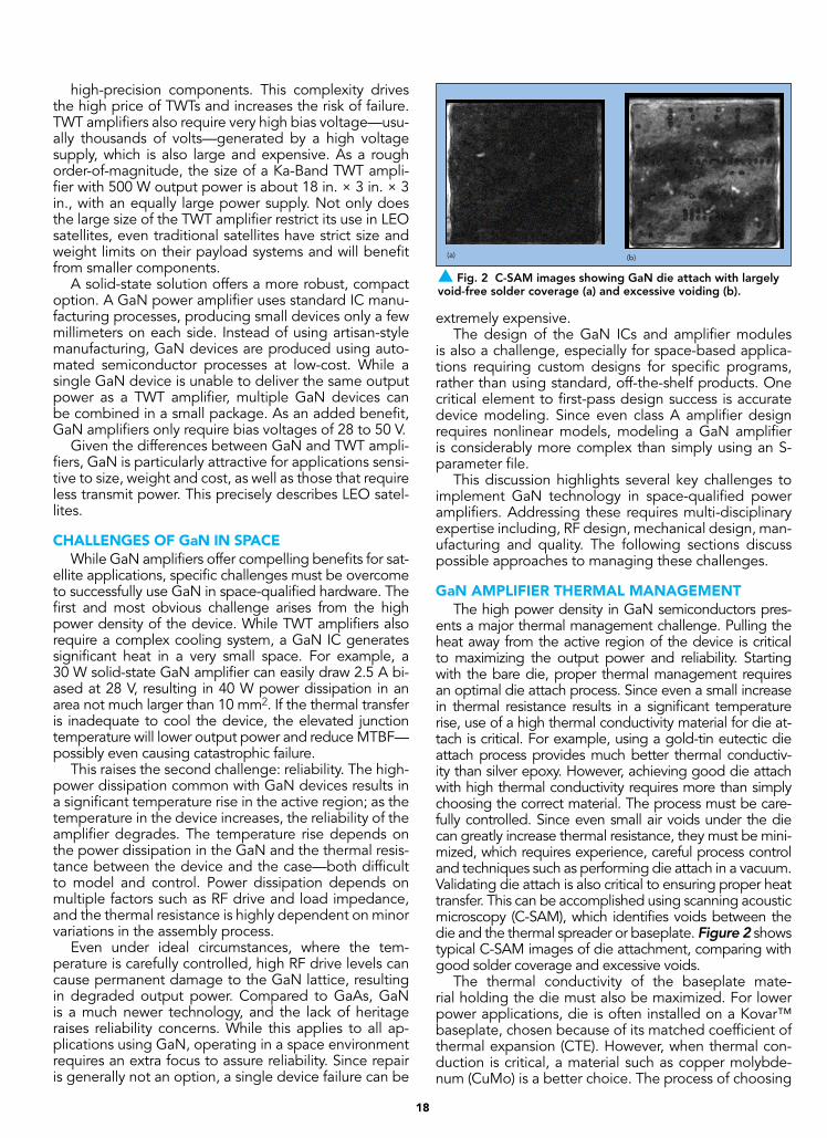
ents a major thermal management challenge. Pulling the heat away from the active region of the device is critical to maximizing the output power and reliability. Starting with the bare die, proper thermal management requires an optimal die attach process. Since even a small increase in thermal resistance results in a significant temperature rise, use of a high thermal conductivity material for die at-tach is critical. For example, using a gold-tin eutectic die attach process provides much better thermal conductiv-ity than silver epoxy. However, achieving good die attach with high thermal conductivity requires more than simply choosing the correct material. The process must be care-fully controlled. Since even small air voids under the die can greatly increase thermal resistance, they must be mini-mized, which requires experience, careful process control and techniques such as performing die attach in a vacuum. Validating die attach is also critical to ensuring proper heat transfer. This can be accomplished using scanning acoustic microscopy (C-SAM), which identifies voids between the die and the thermal spreader or baseplate. Figure 2 shows typical C-SAM images of die attachment, comparing with good solder coverage and excessive voids.
The thermal conductivity of the baseplate mate-rial holding the die must also be maximized. For lower power applications, die is often installed on a Kovar™ baseplate, chosen because of its matched coefficient of thermal expansion (CTE). However, when thermal con-duction is critical, a material such as copper molybde-num (CuMo) is a better choice. The process of choosing
s Fig. 2 C-SAM images showing GaN die attach with largely void-free solder coverage (a) and excessive voiding (b).
(a) (b)

19
materials to optimize the thermal conductivity of each interface continues through the entire design, from device to system packaging.
While this thermal design approach is used for GaN amplifier designs regardless of application, it is particu-larly important for space-qualified hardware. The size and weight constraints common to space programs in-crease power density by limiting the volume, while the reliability requirements for space operation require max-imum cooling of the active devices.
GaN RELIABILITYReliability is often characterized by the failure rate
versus time, which often looks like a “bathtub” and has been called the “bathtub curve” (see Figure 3). Typi-cally, the majority of failures occur early in the product’s life or after considerable use. Early failures are usually caused by a manufacturing defect, either during device fabrication or subsequent assembly. On the other side of the graph, the uptick in failures represents the de-vice wearing out near the end of its lifetime. To optimize and assure reliability, each of these failure types must be considered.
In the case of GaN, early failures are reduced through manufacturing process control, wafer screening and burn-in. Process control includes repeatable die attach, discussed above, and control of all aspects of the manu-facturing process. Clear documentation and operator training are critical, as well as environmental controls, such as reducing the risk for damage caused by electro-static discharge (ESD). With minimal performance varia-tion across a GaN wafer, sample testing can be used to qualify a wafer, improving confidence in the device’s reliability before committing the devices from a wafer to assembly. Depending on the program, wafer screen-ing may require accelerated life testing and destructive physical analysis. The risk of early failure can be reduced further through 100 percent burn-in screening. Using burn-in, amplifiers are biased and placed in an oven at elevated temperature for a specified time to stress the active devices. Burn-in screening will weed out the early failures, reducing the probability of failure in the field.
To quantify the length of operational time before wear-out failures occur, the MTBF of the amplifier is calculated. This calculation uses multiple factors such as device temperature, bias and environmental condi-
tions and is based on empirical data from accelerated life testing. To maximize the MTBF, the device cooling must be optimized, as described earlier.
While the radiation encountered in space creates an-other reliability risk, the high molecular bond strength of GaN results in a higher radiation tolerance than GaAs and silicon.
CUSTOM GaN AMPLIFIER DESIGNSince space missions usually require amplifiers with
unique frequencies, bandwidths, output power and reli-ability, they usually require custom designs rather than off-the-shelf products. Since the production volumes are typically low, the cost of the development must be mini-mized as well as the unit cost, to keep the total program cost low. One of the best ways to reduce design time and cost is to improve first-pass success, which requires accurate device modeling.
Nonlinear device modeling for power amplifier de-sign is always a challenge; since GaN is a newer technol-ogy, its models are less mature. To address this lack of accurate models, the design engineer has several op-tions:• Rely on measured load-pull data to determine the
ideal output impedance match to optimize the RF power.
• Through experience, adjust the simulation models to improve the accuracy for the specific design condi-tions.
• Substitute a measured, small-signal S-parameter file for the nonlinear model to confirm similar results for linear operation.
SUMMARYSatellite applications will clearly benefit from space-
qualified GaN power amplifiers, which offer size, weight and thermal benefits over TWT amplifiers. However, producing GaN power amplifiers is challenging, par-ticularly with the lack of space heritage. Successful in-sertion requires experience with both the electrical and mechanical aspects of GaN amplifier design, comple-menting space quality levels and requirements such as MIL-PRF-38534 class K. For organizations with both competencies, space-qualified GaN technology offers exciting new market opportunities.n
DecreasingFailureRate
Early”Infant Mortality” Failure
ConstantFailureRate
IncreasingFailureRate
Failu
re R
ate
Constant (Random)Failures
Observed FailureRate
Wear OutFailures
Time
s Fig. 3 Reliability bathtub curve. Source: Wikimedia.

Qorvo’s wide portfolio of satcom products offer innovative solutions that are high performing, reliable and easy to integrate.
To learn more, visit RellPower.com/QorvoSatcom
Qorvo’s QPA2626 is a packaged, high-performance, low noise amplifier fabricated on Qorvo’s production 90nm pHEMT (QPHT09) GaAs process. Covering 17-22 GHz, the QPA2626 provides 25 dB small signal gain and P1dB of 20 dBm, while supporting a noise figure of 1.3 dB and IM3 levels of -55 dBc (at Pout=0 dBm/tone). Packaged in a small 4x4mm plastic overmold QFN, the QPA2626 is matched to 50 ohms with integrated DC blocking caps on both I/O ports for easy handling and simple system integration. LEARN MORE
QPA2626
Powerfully EngineeredSolutions for SatcomSolving RF complexity for mission critical applications
© Qorvo, Inc. | 2019. QORVO is a registered trademark of Qorvo, Inc. in the U.S. and in other countries.