nasa eee parts and packaging (nepp) program · nasa eee parts & packaging program mews 19...
TRANSCRIPT
NASA EEE Parts and Packaging (NEPP) Program
NASA EEE Parts and Packaging (NEPP) Program
An Overview of Current and Future Activities
An Overview of Current and Future Activities
Kenneth A. LaBelNASA/GSFCApplied Engineering and Technology Directorate
Kenneth A. LaBelNASA/GSFCApplied Engineering and Technology Directorate
Michael J. SampsonNASA/GSFCOffice of System Safety and Mission Assurance
Michael J. SampsonNASA/GSFCOffice of System Safety and Mission Assurance
CO-MANAGERSCO-MANAGERS
Presentation to 19th Annual Microelectronics Workshop (MEWS 19)
JAXA, Tsukuba, Japan, October 26, 2006
Presentation to 19th Annual Microelectronics Workshop (MEWS 19)
JAXA, Tsukuba, Japan, October 26, 2006
NASA EEE Parts & Packaging Program
10/26/06 (2)MEWS 19
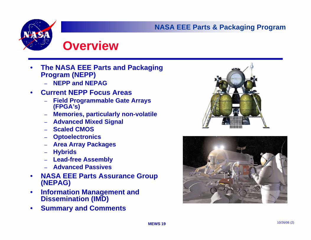
Overview• The NASA EEE Parts and Packaging
Program (NEPP)– NEPP and NEPAG
• Current NEPP Focus Areas– Field Programmable Gate Arrays
(FPGA’s)– Memories, particularly non-volatile– Advanced Mixed Signal– Scaled CMOS– Optoelectronics– Area Array Packages– Hybrids– Lead-free Assembly– Advanced Passives
• NASA EEE Parts Assurance Group (NEPAG)
• Information Management and Dissemination (IMD)
• Summary and Comments

NASA EEE Parts & Packaging Program
10/26/06 (3)MEWS 19
NEPP Mission and Focus
• The NEPP mission is to provide guidance to NASA for the selection and application of microelectronics technologies, to improve understanding of the risks related to the use of these technologies in the space environment and to ensure that appropriate research is performed to meet NASA mission assurance needs.
• NEPP subset: NASA Electronic Parts Assurance Group (NEPAG)
– Focuses on daily needs of parts assurance knowledge-base
NASA Technology Readiness Levels (TRLs)
NEPPinterestrange
NEPAGinterestrange

NASA EEE Parts & Packaging Program
10/26/06 (4)MEWS 19
NEPP Project Assistance
– MAP• Single Event Transients (SETs) –
NASA alert– TERRA
• Optocouplers, Solid State Recorders (SSR), High Gain Antenna anomaly
– AURA• Oscillators
– AQUA• Interpoint DC-DC converters
– TRMM, XTE• SSRs, Fiber Optics
– TOPEX/Poseidon• Optocouplers
– SeaStar• SSRs
– Launch Vehicles• Optocouplers
– Suborbital• Parts screening
– LWS• FPGAs, memories
– Hubble Space Telescope• Optocouplers, Capacitors, SSRs,
Fiber Optic Data Bus (FODB), Xilinx FPGAs, detector technologies
– Hubble Robotic Servicing• Processors, memories, FPGAs,
packaging– JWST
• Detector technologies, memories– Cassini
• Interpoint DC-DC converters, optocouplers, processors
– AXAF/Chandra• Optics
– SWIFT• ACTEL FPGAs
– MER, MRO• ELDRS, Processors, Memories,
Packaging, FPGAs– ISS
• Fiber optics, wire/cable– Shuttle
• ACTEL FPGAs, capacitors– GLAST
• Lasers

NASA EEE Parts & Packaging Program
10/26/06 (5)MEWS 19
NEPP CollaborationsGovernment partners
– Department of Defense• Defense Threat Reduction Agency
(DTRA)• Air Force Research Laboratory
(AFRL)• Air Force Space and Missile
Command (AFSMC)• Missile Defense Agency (MDA)• Defense Advanced Research Projects
Agency (DARPA)• NAVSEA• NAVAIR• Naval Research Laboratory• US Army Strategic and Missile
Defense Command (USASMDC)• OGA
– Department of Energy• Sandia National Laboratories• Lawrence Livermore National
Laboratories• Brookhaven National Laboratories• Los Alamos National Laboratories
– National Science Foundation• National Superconducting Cyclotron
Laboratory– ESA– JAXA– CNES
Industry partners– Actel– Lambda/International Rectifier– Interpoint– Vishay– Presidio– BAE Systems– Honeywell– Aeroflex– Intersil– Xilinx– IBM– Freescale (formerly Motorola)– Cardinal– LSI Logic– Ball Aerospace– ATK– Micro RDC– Seakr– Maxwell– Texas Instruments– SAIC– Boeing

NASA EEE Parts & Packaging Program
10/26/06 (6)MEWS 19
NEPP Focus Areas
• Starting in FY05, the NEPP Program was organized around these high demand focus areas:
– Field Programmable Gate Arrays (FPGA’s)– Memories, particularly non-volatile– Advanced Mixed Signal– Scaled CMOS– Optoelectronics– Area Array Packages– Hybrids– Lead-free Assembly– Advanced Passives

NASA EEE Parts & Packaging Program
10/26/06 (7)MEWS 19
NEPP Funding DistributionRadiation
39%IMD4%
Packaging9%
Reliability33%
NEPAG15%
LaRC2% KSC
0%
GRC6%
JPL34%
JSC5%MSFC
6%GSFC47%
Scaled CMOS7%
Adv Mixed Signal
8%
Other37%
FPGA's14%
Memory12%
Area Arrays6%
Adv Passives2%
Photonics6%Hybrids
4%
Lead-free4%
NASA EEE Parts & Packaging Program
10/26/06 (8)MEWS 19
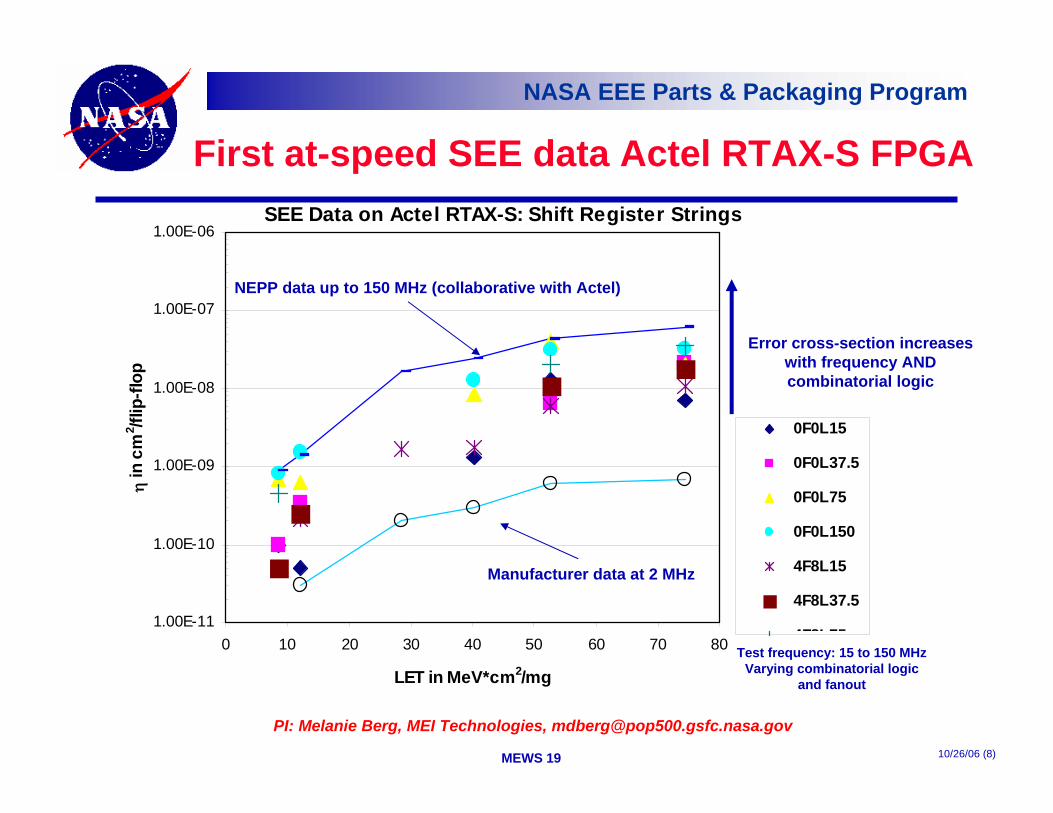
First at-speed SEE data Actel RTAX-S FPGA
Test frequency: 15 to 150 MHzVarying combinatorial logic
and fanout
Manufacturer data at 2 MHz
PI: Melanie Berg, MEI Technologies, [email protected]
NEPP data up to 150 MHz (collaborative with Actel)
Error cross-section increaseswith frequency ANDcombinatorial logic
SEE Data on Actel RTAX-S: Shift Register Strings
1.00E-11
1.00E-10
1.00E-09
1.00E-08
1.00E-07
1.00E-06
0 10 20 30 40 50 60 70 80
LET in MeV*cm2/mg
η in
cm
2 /flip
-flop
0F0L15
0F0L37.5
0F0L75
0F0L150
4F8L15
4F8L37.5
4F8L75

NASA EEE Parts & Packaging Program
10/26/06 (9)MEWS 19PI: Gary Swift, JPL/Caltech, [email protected]
Xilinx Virtex-II Pro 2VP40 Inventory of Storage Elements and their Mitigation Techniques
CLB, 10462828, 71.534%
User FF, 43632, 0.298%
Half Latch, 278,724, 1.906%
BRAM, 3538944, 24.196%
D Cache, 131072, 0.896%
I Cache, 131072, 0.896%
GPR, 1024, 0.007%
SPR, 1728, 0.012%
Gasket, 37296, 0.255%
PowerPC 2.066%
Complete SEU Characterization of Virtex II-Pro FPGAs
Inventory of
Upsetable Elements –
Xilinx XQR2VP40
NEPP works collaboratively withthe Xilinx Radiation Test Consortia (XRTC)
Ones
1E-10
1E-9
1E-8
1E-7
1E-6
0 10 20 30 40
LET (MeV per mg/cm2)
Cro
ss S
ectio
n (c
m2 /b
it)
Zeros
General Purpose Registers XQR2VP40 embedded PPC405 core

NASA EEE Parts & Packaging Program
10/26/06 (10)MEWS 19
0 5 10 20 30 50 75 100
Static 1
Static 3
Dynamic 1 1.00E+00
1.00E+01
1.00E+02
1.00E+03
1.00E+04
1.00E+05
1.00E+06
1.00E+07
1.00E+08
1.00E+09
1.00E+10
Num
ber o
f bits
in e
rror
TID in krad-SiO2
DUT and test type
Micron 2Gb NAND Flash - Number of Bad Bits90 nm CMOS
State-of-the-art Flash Memory Evaluation
PI: Tim Oldham, QSS Corp, [email protected]
Note mode dependence of results.Novel error mode observed
NEPP evaluates state-of-the-art and emerging non-volatile memories (NVMs) focusing on:- Technology, architecture, and application issues
0 10 20 30 50 75 100 150
Static 1
Static 3
Reset 1Reset 3
1.00E+00
1.00E+01
1.00E+02
1.00E+03
1.00E+04
1.00E+05
1.00E+06
1.00E+07
1.00E+08
1.00E+09
1.00E+10
Num
ber o
f bits
in e
rror
TID in krad-SiO2
Test DUT and Type
ST 1Gb NAND Flash - Number of Bad Bits110 nm CMOS

NASA EEE Parts & Packaging Program
10/26/06 (11)MEWS 19
State-of-the-art SDRAM Memory Evaluation –Challenges for test preparation and data collection/analysis
θ
X-Ray Photo of a DUT
Determining effective LET as a function of angle requires correcting for the energy lost by the ion as it traverses overburden to the sensitive volume, as well the usual 1/cosθ dependence.
NEPP evaluates state-of-the-art and emerging SDRAMs focusing on:- Technology, architecture, and test methodology issues
PI: Ray Ladbury, NASA-GSFC, [email protected]

NASA EEE Parts & Packaging Program
10/26/06 (12)MEWS 19
Evaluating SEE Rad Hard by Design (RHBD) Approaches:Dramatic SEE improvements in SEE sensitivity on 8HP HBT
PI: Paul Marshall: [email protected]
Limiting Cross-section!
SiGe Radiation Evaluation and Modeling –
Working collaboratively with technology development programs

NASA EEE Parts & Packaging Program
10/26/06 (13)MEWS 19
Scaled CMOS Reliability
Impact of Technology Scaling on Lifetime Reliability –Processor modeling predictions from various failure mechanisms as a function of technology. (U of I, IBM)
7681651.70.25
5281651.60.15
1.5
588165/1551.40.13
Time to 0.1% Device-Bit
Failures (Hrs)Temp CVratio
(Vapp/Vnom)
Tech. Node (um)
SRAM time to failure as a result of step stress testing 125*C to 165*C (10*C steps) and high voltage ramp stress (0.1Vdd) at constant frequency. (JPL)
Decapsulatedoptical overview -Post stress test 0.15um, 4M SRAM. (JPL)
Modeling TrendsAccelerated Stress Testing
Failure Analysis
PI: Mark White, JPL, [email protected]

NASA EEE Parts & Packaging Program
10/26/06 (14)MEWS 19
Photon emissions between Vcc and Vss. Characteristic failure site across technologies (JPL).
Buffer/voltage regulation circuitry protects the actual memory cells and damage is concentrated on the input transistors of the devices (regardless of technology scaling).
LeakageSite
Failure Analysis
Focused Ion Beam close-up of a failure site (0.15um 4M SRAM) post accelerated stress test. Failure Mechanism: Stress migration in the input transistors - buffer/voltage regulation circuitry, not in the memory cells (JPL).
Stress Migration
Scaled CMOS Reliability - 2

NASA EEE Parts & Packaging Program
10/26/06 (15)MEWS 19
Scaled CMOS Reliability - 3
Reliability Trends and Early Wearout: Normalized Commercial Manufacturer’s data
Industry data showing both increasing failure rate and decreasing product lifetime with progressive commercial technologies (UMD).
1.E+01
1.E+02
1.E+03
1.E+02 1.E+03 1.E+04 1.E+05 1.E+06 1.E+07 1.E+08
Time(equivalent hours)
Acceptable for Commercial Applications
Required for Avionics
Equivalent Burn-In time.
20002005
2010Normalized Number of
Failures

NASA EEE Parts & Packaging Program
10/26/06 (16)MEWS 19
• Provide guidelines for qualification and application of flight critical photonic components
• Disseminate lessons learned• Enhance TRL of fiber laser and
semiconductor laser components • FY06 focus: commercial parts for space
with emphasis on high power laser diode arrays, fiber amplifier components, optical fiber cable, and optical fiber array interconnection
Vibration Test; MTP Connector
Fiber array in AVIM evaluations
fiber cable in moving gimbal test
FY06 Highlights• ESA/NASA Workshop 2005 & 2006, Web access to presentations; included participation from JAXA.• High Power Laser Diode Array Qualification and Guidelines for Space Environments Draft coordinated
with GSFC, LaRC and Laser Risk Reduction Prgm.• Qualification and Issues with Space Flight Laser Systems and Components, SPIE Solid State Lasers,
Vol. 6100, Jan. 2006, • Space Requirements for Fiber Optic Components Testing and Lessons Learned, SPIE Europe Vol. 6193,
April 2006.• Space Qualification of a Multi-Fiber Ribbon Cable and Connector Array Assembly, SPIE Photonics for
Space Environments XI, Vol. 6308, Aug 2006.• Photonic Component Qualification and Implementation Activities at NASA, SPIE Vol. 6308, Aug 2006.
PI: Melanie Ott,, NASA-GSFC, [email protected]
Optoelectronics for Space Environments

NASA EEE Parts & Packaging Program
10/26/06 (17)MEWS 19
Optoelectronics - The ESA-NASA Workshops
Co-Chairs: Dr. Nikos Karafolas, ESTEC-ESA, Melanie N. Ott, NASA-NEPP
Workshop 1Fiber Optic Technologies for Space-Lessons Learned,
October 2005.
Workshop 2Qualification of Technologies and Lessons Learned
from LIDAR and Altimetry MissionsJune 2006Mission Presentations Included:
HayabusaLIDAR at
Itokawa AsteroidJAXA
ADM-AeolusWind LIDAR
ESAMESSENGER
Mercury Laser AltimeterNASA GSFC
ICESATGeoscience Laser
AltimeterNASA GSFC Calipso
Ball/FibertekNASA LaRC
LROLaser Ranging/LOLA
NASA GSFC
URL for Websites with Presentations: http://misspiggy.gsfc.nasa.gov/photonicshttps://escies.org/public/conferences/photonics/1/index.xmlhttp://nepp.nasa.gov

NASA EEE Parts & Packaging Program
10/26/06 (18)MEWS 19
Objective:• Qualification guidelines for high
I/O area array packages Testing to develop guidelines:
– Thermal cycles-to-failure using:• NASA thermal profile (-55/100°C)• and military cycle (-55/125°C)• for > 1,000 thermal cycles
– ~ 50 packages 700-1200 I/O– Also for a few samples:
•-65/150°C• Mars profile -120/85°C
– Data analysis plus literature review for key design and process controls.
– Body of knowledge and test matrix developed for High I/O packages
– Designed experiment and test matrix for low pitch/High I/Os
Various CCGA >1000 I/Os. Have been thermal cycled under various regimes
Highlights:•Publications, IPC APEC, IEEE CPMT, Microelectronic Reliability Journal (in print- Dec 2006)
•Book chapter-2006•Papers on NEPP web site
Reliability of High I/O Area Array Packages

NASA EEE Parts & Packaging Program
10/26/06 (19)MEWS 19
CCGA717 I/O
PBGA728 I/O
PI: Reza Ghaffarian, JPL, [email protected]

NASA EEE Parts & Packaging Program
10/26/06 (20)MEWS 19
Copper Spiral Wrapped Columns – SIX SIGMA
Copper provides reinforcement and redundant conductive path

NASA EEE Parts & Packaging Program
10/26/06 (21)MEWS 19
DC/DC Converter Risk Mitigation
NEPP is developing:• Test and evaluation guidelines• Application guidelines• Databases for information
exchange
Using Zin measurements to find safe operating zone
Failures in spacecraft range from:• Manufacturer installed defects
• Workmanship• Inconsistent magnetics
design/control• Unqualified replacement of
elements• Incorrect screening of elements• Application errors
• Under-loading• Impedance mismatching• Incorrect synchronization
• Confusion about how• Far outside of the nominal
operating conditions the part can be safely used
• Load derating actually adds risk
PI: Jeannette Plante, Dynamic Range, [email protected]
http://nepp.nasa.gov/dcdc
Input Impedance
-30
-20
-10
0
10
20
30
40
1.00E+02 6.33E+02 4.01E+03 2.54E+04 1.61E+05
Frequency
dB O
hm
0
510
15
20
2530
35
40
Ohm
dB Ohm10 (̂dB Ohm/20)
Incomplete information has directly contributed to failures
NASA EEE Parts & Packaging Program
10/26/06 (22)MEWS 19
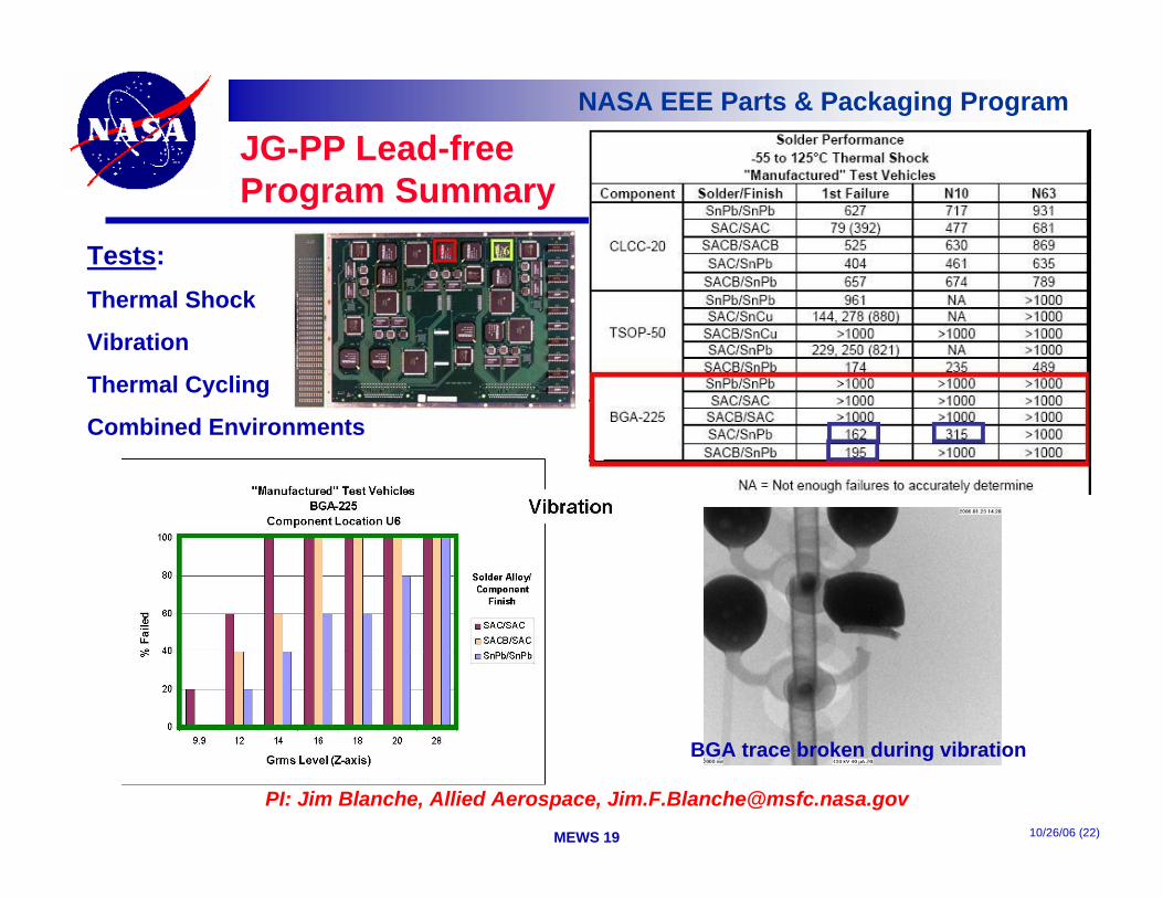
Tests:Thermal Shock
Vibration
Thermal Cycling
Combined Environments
JG-PP Lead-free Program Summary
BGA trace broken during vibration
PI: Jim Blanche, Allied Aerospace, [email protected]

NASA EEE Parts & Packaging Program
10/26/06 (23)MEWS 19
Polymer Tantalum CapacitorsBetter at High Frequency
0.01
0.1
1
10
100
101 102 103 104 105 1060
0.25x10⁻⁴
0.50x10⁻⁴
0.75x10⁻⁴
1.00x10⁻⁴
CapacitanceImpedanceESR
Ta Poly
Ta MnO2
Ta MnO2
Ta Poly
EKR, 7/18/2006Frequency (Hz)
Impe
danc
e an
d E
SR
(Ω)
Cap
acita
nce
Exc
ludi
ng 3
.0nH
Sel
f Ind
ucta
nce
(F)
Capacitance, Impedance, and ESR for 100uF, 10V Tantalum Capacitors (Polymer vs MnO2)

NASA EEE Parts & Packaging Program
10/26/06 (24)MEWS 19
0
0.00005
0.00010
0.00015
101 102 103 104 105 106
125C85C25C-15C-55C-90C-130C-193C
EKR, 7/24/2006Frequency (Hz)
Cap
acita
nce
(F)
Capacitance vs. Frequency at Various Temperatures (100uF, 10V Tantalum Polymer)
0
0.00005
0.00010
0.00015
101 102 103 104 105 106
125C85C25C-15C-55C-90C-130C-193C
EKR, 7/24/2006Frequency (Hz)
Cap
acita
nce
(F)
Capacitance vs. Frequency at Various Temperatures (100uF, 10V Tantalum MnO2)
Polymer Tantalum CapacitorsBetter at High Frequency and Over Temperature Too!
Capacitance
PI: Erik Reed, JPL, [email protected]

NASA EEE Parts & Packaging Program
10/26/06 (25)MEWS 19
Polymer Tantalum CapacitorsBetter at High Frequency and Over Temperature Too!
0.01
0.1
1
10
101 102 103 104 105 106
125C85C25C-15C-55C-90C-130C-193C
EKR, 7/24/2006Frequency (Hz)
ES
R (Ω
)
ESR vs. Frequency at Various Temperatures (100uF, 10V Tantalum MnO2)
0.01
0.1
1
10
101 102 103 104 105 106
125C85C25C-15C-55C-90C-130C-193C
EKR, 7/24/2006Frequency (Hz)
ES
R (Ω
)
ESR vs. Frequency at Various Temperatures (100uF, 10V Tantalum Polymer)
Equivalent Series Resistance (ESR)
Life Testing is in Progress
NASA EEE Parts & Packaging Program
10/26/06 (26)MEWS 19
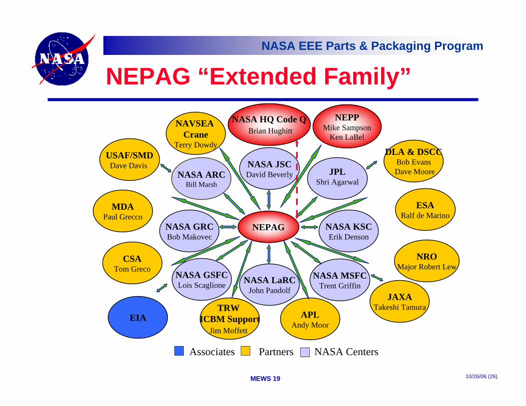
NEPAG “Extended Family”
NEPAG
NASA ARCBill Marsh
JPLShri Agarwal
NASA GSFCLois Scaglione
NASA MSFCTrent Griffin
NASA GRCBob Makovec
NASA KSCErik Denson
NASA LaRCJohn Pandolf
NAVSEA Crane
Terry DowdyUSAF/SMD
Dave Davis
JAXATakeshi Tamura
ESARalf de Marino
DLA & DSCCBob EvansDave Moore
EIATRW
ICBM SupportJim Moffett
APLAndy Moor
NASA HQ Code QBrian Hughitt
Associates Partners NASA Centers
NASA JSCDavid Beverly
CSATom Greco
NEPPMike Sampson
Ken LaBel
MDAPaul Grecco
NROMajor Robert Lew

NASA EEE Parts & Packaging Program
10/26/06 (27)MEWS 19
NEPAG Tasks and Activities
• Weekly US and Monthly international telecons– Typically 30+ participants– JAXA and ESA are on international calls
• Audits– Over 80 NEPAG supported US and international in FY06 Mostly
space level, JANS, Class V and K
• Participation in MIL and non-government specification and standards activities:
– EIA G11, G12, JEDEC, IPC
• Lead-free:– Executive Lead-Free (ELF) IPT, Lead-free Electronics in Aerospace
Project (LEAP), JG-PP, CALCE (University of Maryland) etc.– Metal whisker website: http://nepp.nasa.gov/whisker– Continued whisker research

NASA EEE Parts & Packaging Program
10/26/06 (28)MEWS 19
18-mm Long Tin Whisker!!!
Photo Credit: James D. Stewart,M&P Failure Analysis LaboratoryThe Boeing Company Logistics Depot
PI: Jay A. Brusse, QSS, [email protected]

NASA EEE Parts & Packaging Program
10/26/06 (29)MEWS 19
Tin Whiskers on PCB Card GuidesRef: “Tin Whiskers Found on ATVC S/N 0034”, Don McCorvey, March 8, 2006

NASA EEE Parts & Packaging Program
10/26/06 (30)MEWS 19
A Pb-Free Strategy for Space
• Require traditional tin-lead solders for all electronic assembly except when justified by technical need (such as a high melt point)
– Approved GEIA-STD-0005-1 plan to define rules and controls– SAC and other “new” alloys will require special and exceptional
rationale• Require all tin-based platings and protective finishes to have a
minimum of 3% Pb content unless:• A persuasive rationale is provided• Tin whisker mitigation strategy is supported by data and approved by NASA• GEIA-STD-0005-2, “Control Level 2C” because required by part number• Alternative, “wait-and-see” is CHAOS
• Perform checks for Pb content at incoming to prevent “escapes”• Use at least two analysis methods such as XRF for a quick look and
SEM/EDAX for the final disposition
• Ensure suppliers have adequate materials checks and controls• Continue to Study Whiskers Because Mistakes Will Be Made

NASA EEE Parts & Packaging Program
10/26/06 (31)MEWS 19
MIL Specification Standardization
• Memorandum of Understanding (MOU)– Government HiRel/Space working on agreement with
Defense Supply Center Columbus (DSCC) – Defines roles/responsibilities/expectations for participation
in MIL auditing process– USAF, NRO, MDA, Navy, NASA– Working out authorization details
• M38535 Engineering Practices (EP) Study– August industry/government meeting was very productive– Revised draft almost be ready for official coordination– Most significant revision since “Acquisition Reform” in
mid-1990’s– Addresses outsourcing control issues– New Technology Insertion approach still needs formulation
NASA EEE Parts & Packaging Program
10/26/06 (32)MEWS 19
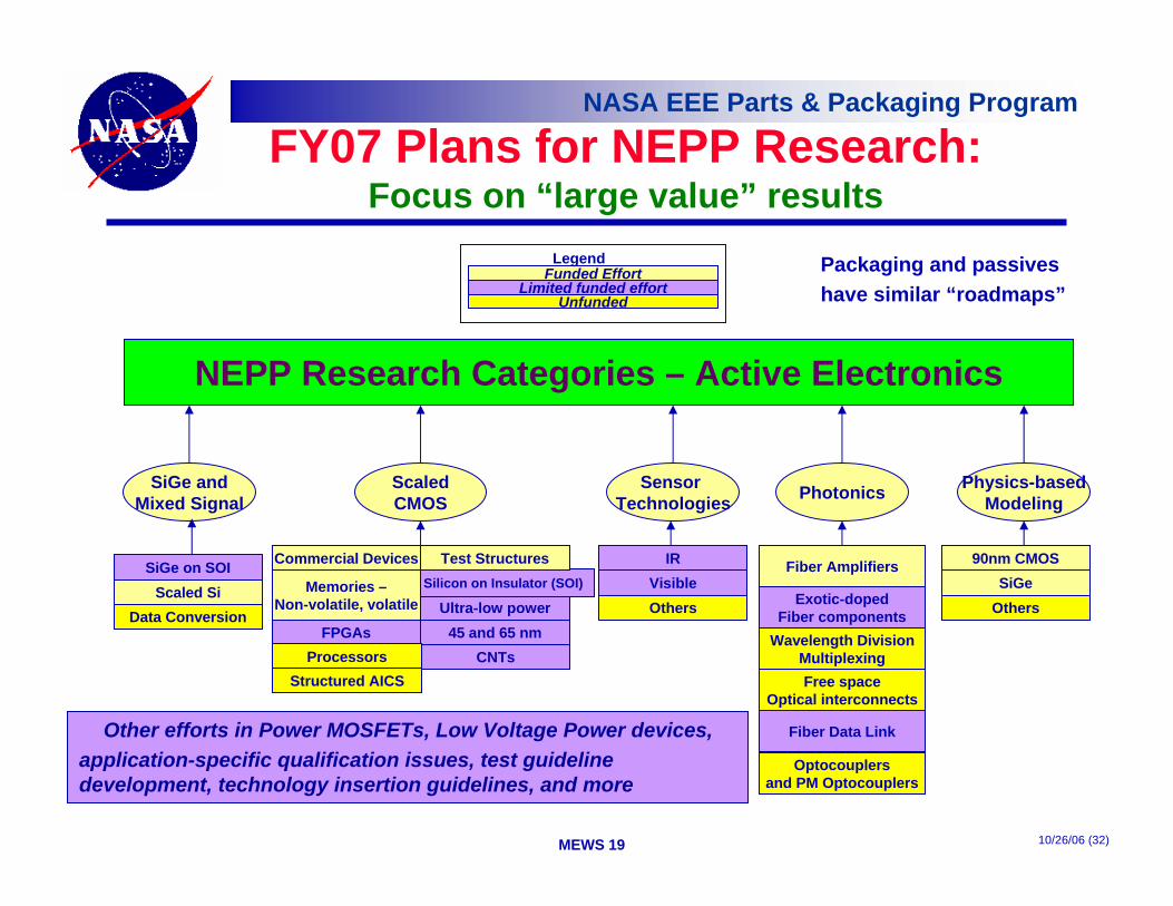
FY07 Plans for NEPP Research:Focus on “large value” results
SiGe andMixed Signal PhotonicsScaled
CMOSSensor
TechnologiesPhysics-based
Modeling
Fiber Amplifiers
Exotic-dopedFiber components
Wavelength DivisionMultiplexingFree space
Optical interconnects
Fiber Data Link
NEPP Research Categories – Active Electronics
Ultra-low powerSilicon on Insulator (SOI)
IRVisibleOthers
Funded Effort
UnfundedLimited funded effort
Legend
Test StructuresCommercial Devices
Memories –Non-volatile, volatile
FPGAs 45 and 65 nm
90nm CMOSSiGe
Others
Other efforts in Power MOSFETs, Low Voltage Power devices,application-specific qualification issues, test guideline development, technology insertion guidelines, and more
Processors CNTsStructured AICS
Packaging and passiveshave similar “roadmaps”
Optocouplersand PM Optocouplers
SiGe on SOIScaled Si
Data Conversion

NASA EEE Parts & Packaging Program
10/26/06 (33)MEWS 19
IMDInformation Management & Dissemination
IMD on the Web:• Provides information regarding
EEE parts’:• Reliability• Performance• Availability• Application• Radiation characteristics• Packaging• Cost
• Coordinates task reporting• Methodically disseminates
information generated by NEPP• Maintains the website• For its NASA customers:
• Designers• Specialist researchers• Project engineers• Scientists• Program managers.
Manager: Dr. Lois Scaglione, GSFC, [email protected]

NASA EEE Parts & Packaging Program
10/26/06 (34)MEWS 19
Summary and Comments• NEPP Provides Critical Guidance for Flight Projects
– Challenge: Keeping ahead of the demand• NEPP Partners Throughout the Aerospace Industry
– NEPP/NEPAG leads in information exchange across the community• NEPP Strives to Develop Cost-Effective Qualification Methods
– Challenge: The ever-increasing cost of doing business• NEPP is focusing on high-demand/high-return technologies with
immediate value to flight projects• New training modules are required for new technology insertion
– NEPP has more than just parts, packaging, and radiation challenges• Currently collaborating with CNES, ESA and others on radiation training
class (SERESSA)– NEPP is increasing its university presence
• Shortfall of qualified parts, packaging, and radiation specialists- Example: Difficulty in finding US citizens for radiation positions
• Scholarships, post-doc opportunities, etc are being considered
NASA EEE Parts & Packaging Program
10/26/06 (34)MEWS 19