nanotube growth and characterization - springer
TRANSCRIPT
Nanotube Growth and Characterization
Hongjie Dai
Department of Chemistry, Stanford UniversityStanford, CA 94305-5080, [email protected]
Abstract. This chapter presents a review of various growth methods for carbonnanotubes. Recent advances in nanotube growth by chemical vapor deposition(CVD) approaches are summarized. CVD methods are promising for producinghigh quality nanotube materials at large scales. Moreover, controlled CVD growthstrategies on catalytically patterned substrates can yield ordered nanotube archi-tectures and integrated devices that are useful for fundamental characterizationsand potential applications of nanotube molecular wires.
In 1991, Iijima of the NEC Laboratory in Japan reported the first observa-tion of multi-walled carbon nanotubes (MWNT) in carbon-soot made by arc-discharge [1]. About two years later, he made the observation of Single-WalledNanoTubes (SWNTs) [2]. The past decade witnessed significant research ef-forts in efficient and high-yield nanotube growth methods. The success innanotube growth has led to the wide availability of nanotube materials, andis a main catalyst behind the recent progress in basis physics studies andapplications of nanotubes.
The electrical and mechanical properties of carbon nanotubes have cap-tured the attention of researchers worldwide. Understanding these propertiesand exploring their potential applications have been a main driving force forthis area. Besides the unique and useful structural properties, a nanotube hashigh Young’s modulus and tensile strength. A SWNT can behave as a well-defined metallic, semiconducting or semi-metallic wire depending on two keystructural parameters, chirality and diameter [3]. Nanotubes are ideal sys-tems for studying the physics in one-dimensional solids. Theoretical and ex-perimental work have focused on the relationship between nanotube atomicstructures and electronic structures, electron-electron and electron-phononinteraction effects [4]. Extensive effort has been taken to investigate the me-chanical properties of nanotubes including their Young’s modulus, tensilestrength, failure processes and mechanisms. Also, an intriguing fundamen-tal question has been how mechanical deformation in a nanotube affects itselectrical properties. In recent years, progress in addressing these basic prob-lems has generated significant excitement in the area of nanoscale science andtechnology.
Nanotubes can be utilized individually or as an ensemble to build func-tional device prototypes, as has been demonstrated by many research groups.Ensembles of nanotubes have been used for field emission based flat-panelM. S. Dresselhaus, G. Dresselhaus, Ph. Avouris (Eds.): Carbon Nanotubes,Topics Appl. Phys. 80, 29–53 (2001)c© Springer-Verlag Berlin Heidelberg 2001

30 Hongjie Dai
display, composite materials with improved mechanical properties and elec-tromechanical actuators. Bulk quantities of nanotubes have also been sug-gested to be useful as high-capacity hydrogen storage media. Individual nano-tubes have been used for field emission sources, tips for scanning probe mi-croscopy and nano-tweezers. Nanotubes also have significant potential as thecentral elements of nano-electronic devices including field effect transistors,single-electron transistors and rectifying diodes.
The full potential of nanotubes for applications will be realized until thegrowth of nanotubes can be optimized and well controlled. Real-world ap-plications of nanotubes require either large quantities of bulk materials ordevice integration in scaled-up fashions. For applications such as compositesand hydrogen storage, it is desired to obtain high quality nanotubes at thekilogram or ton level using growth methods that are simple, efficient andinexpensive. For devices such as nanotube based electronics, scale-up willunavoidably rely on self-assembly or controlled growth strategies on surfacescombined with microfabrication techniques. Significant work has been car-ried out in recent years to tackle these issues. Nevertheless, many challengesremain in the nanotube growth area. First, an efficient growth approach tostructurally perfect nanotubes at large scales is still lacking. Second, growingdefect-free nanotubes continuously to macroscopic lengths has been difficult.Third, control over nanotube growth on surfaces should be gained in order toobtain large-scale ordered nanowire structures. Finally, there is a seeminglyformidable task of controlling the chirality of SWNTs by any existing growthmethod.
This chapter summarizes the progress made in recent years in carbonnanotube growth by various methods including arc-discharge, laser ablationand chemical vapor deposition. The growth of nanotube materials by Chem-ical Vapor Deposition (CVD) in bulk and on substrates will be focused on.We will show that CVD growth methods are highly promising for scale-upof defect-free nanotube materials, and enable controlled nanotube growth onsurfaces. Catalytic patterning combined with CVD growth represents a novelapproach to ordered nanowire structures that can be addressed and utilized.
1 Nanotube Growth Methods
Arc-discharge and laser ablation methods for the growth of nanotubes havebeen actively pursued in the past ten years. Both methods involve the conden-sation of carbon atoms generated from evaporation of solid carbon sources.The temperatures involved in these methods are close to the melting temper-ature of graphite, 3000–4000C.
1.1 Arc-Discharge and Laser Ablation
In arc-discharge, carbon atoms are evaporated by plasma of helium gas ig-nited by high currents passed through opposing carbon anode and cathode

Nanotube Growth and Characterization 31
(Fig. 1a). Arc-discharge has been developed into an excellent method forproducing both high quality multi-walled nanotubes and single-walled nano-tubes. MWNTs can be obtained by controlling the growth conditions such asthe pressure of inert gas in the discharge chamber and the arcing current. In1992, a breakthrough in MWNT growth by arc-discharge was first made byEbbesen and Ajayan who achieved growth and purification of high qualityMWNTs at the gram level [5]. The synthesized MWNTs have lengths on theorder of ten microns and diameters in the range of 5-30nm. The nanotubes aretypically bound together by strong van der Waals interactions and form tightbundles. MWNTs produced by arc-discharge are very straight, indicative oftheir high crystallinity. For as grown materials, there are few defects suchas pentagons or heptagons existing on the sidewalls of the nanotubes. Theby-product of the arc-discharge growth process are multi-layered graphiticparticles in polyhedron shapes. Purification of MWNTs can be achieved byheating the as grown material in an oxygen environment to oxidize away thegraphitic particles [5]. The polyhedron graphitic particles exhibit higher ox-idation rate than MWNTs; nevertheless, the oxidation purification processalso removes an appreciable amount of nanotubes.
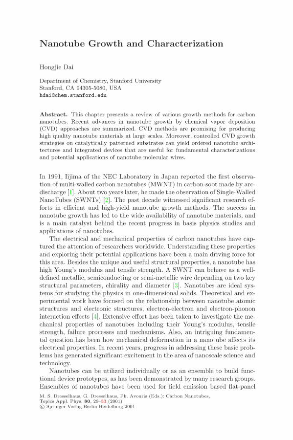
For the growth of single-walled tubes, a metal catalyst is needed in thearc-discharge system. The first success in producing substantial amounts ofSWNTs by arc-discharge was achieved by Bethune and coworkers in 1993 [6].They used a carbon anode containing a small percentage of cobalt catalystin the discharge experiment, and found abundant SWNTs generated in thesoot material. The growth of high quality SWNTs at the 1–10 g scale wasachieved by Smalley and coworkers using a laser ablation (laser oven) method(Fig. 1b) [7]. The method utilized intense laser pulses to ablate a carbontarget containing 0.5 atomic percent of nickel and cobalt. The target wasplaced in a tube-furnace heated to 1200C. During laser ablation, a flowof inert gas was passed through the growth chamber to carry the grownnanotubes downstream to be collected on a cold finger. The produced SWNTsare mostly in the form of ropes consisting of tens of individual nanotubesclose-packed into hexagonal crystals via van der Waals interactions (Fig. 2).The optimization of SWNT growth by arc-discharge was achieved by Journetand coworkers using a carbon anode containing 1.0 atomic percentage ofyttrium and 4.2 at. % of nickel as catalyst [8].
In SWNT growth by arc-discharge and laser ablation, typical by-productsinclude fullerenes, graphitic polyhedrons with enclosed metal particles, andamorphous carbon in the form of particles or overcoating on the sidewalls ofnanotubes. A purification process for SWNT materials has been developedby Smalley and coworkers [9] and is now widely used by many researchers.The method involves refluxing the as-grown SWNTs in a nitric acid solutionfor an extended period of time, oxidizing away amorphous carbon species andremoving some of the metal catalyst species.

32 Hongjie Dai
Fig. 1 a–c. Schematic experi-mental setups for nanotubegrowth methods
The success in producing high quality SWNT materials by laser-ablationand arc-discharge has led to wide availability of samples useful for studyingfundamental physics in low dimensional materials and exploring their appli-cations.
1.2 Chemical Vapor Deposition
Chemical vapor deposition (CVD) methods have been successful in makingcarbon fiber, filament and nanotube materials since more than 10–20 yearsago [10,11,12,13,14,15,16,17,18,19].
1.2.1 General Approach and Mechanism
A schematic experimental setup for CVD growth is depicted in Fig. 1c. Thegrowth process involves heating a catalyst material to high temperaturesin a tube furnace and flowing a hydrocarbon gas through the tube reactorfor a period of time. Materials grown over the catalyst are collected upon
Nanotube Growth and Characterization 33
Fig. 2 a,b. Single-wallednanotubes grown by laserablation (courtesy ofR. Smalley)
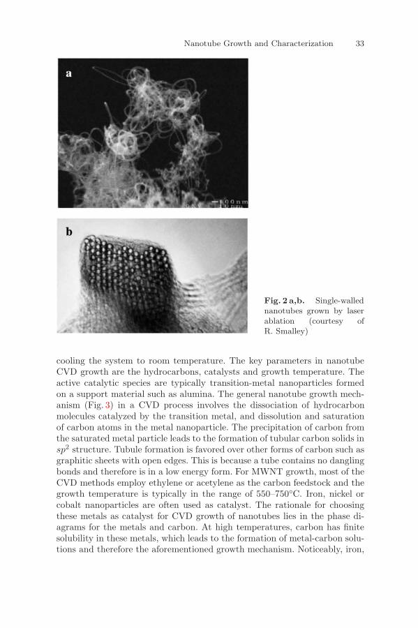
cooling the system to room temperature. The key parameters in nanotubeCVD growth are the hydrocarbons, catalysts and growth temperature. Theactive catalytic species are typically transition-metal nanoparticles formedon a support material such as alumina. The general nanotube growth mech-anism (Fig. 3) in a CVD process involves the dissociation of hydrocarbonmolecules catalyzed by the transition metal, and dissolution and saturationof carbon atoms in the metal nanoparticle. The precipitation of carbon fromthe saturated metal particle leads to the formation of tubular carbon solids insp2 structure. Tubule formation is favored over other forms of carbon such asgraphitic sheets with open edges. This is because a tube contains no danglingbonds and therefore is in a low energy form. For MWNT growth, most of theCVD methods employ ethylene or acetylene as the carbon feedstock and thegrowth temperature is typically in the range of 550–750C. Iron, nickel orcobalt nanoparticles are often used as catalyst. The rationale for choosingthese metals as catalyst for CVD growth of nanotubes lies in the phase di-agrams for the metals and carbon. At high temperatures, carbon has finitesolubility in these metals, which leads to the formation of metal-carbon solu-tions and therefore the aforementioned growth mechanism. Noticeably, iron,

34 Hongjie Dai
Fig. 3. Two general growthmodes of nanotube in chemi-cal vapor deposition. Left di-agram: base growth mode.Right diagram: tip growthmode
cobalt and nickel are also the favored catalytic metals used in laser ablationand arc-discharge. This simple fact may hint that the laser, discharge andCVD growth methods may share a common nanotube growth mechanism,although very different approaches are used to provide carbon feedstock.
A major pitfall for CVD grownMWNTs has been the high defect densitiesin their structures. The defective nature of CVD grown MWNTs remainsto be thoroughly understood, but is most likely be due to the relativelylow growth temperature, which does not provide sufficient thermal energyto anneal nanotubes into perfectly crystalline structures. Growing perfectMWNTs by CVD remains a challenge to this day.
1.2.2 Single-Walled Nanotube Growth and Optimization
For a long time, arc-discharge and laser-ablation have been the principalmethods for obtaining nearly perfect single-walled nanotube materials. Thereare several issues concerning these approaches. First, both methods rely onevaporating carbon atoms from solid carbon sources at ≥ 3000C, whichis not efficient and limits the scale-up of SWNTs. Secondly, the nanotubessynthesized by the evaporation methods are in tangled forms that are diffi-cult to purify, manipulate and assemble for building addressable nanotubestructures.
Recently, growth of single-walled carbon nanotubes with structural perfec-tion was enabled by CVD methods. For an example, we found that by usingmethane as carbon feedstock, reaction temperatures in the range of 850–1000C, suitable catalyst materials and flow conditions one can grow highquality SWNT materials by a simple CVD process [20,21,22,23]. High tem-

Nanotube Growth and Characterization 35
perature is necessary to form SWNTs that have small diameters and thus highstrain energies, and allow for nearly-defect free crystalline nanotube struc-tures. Among all hydrocarbon molecules, methane is the most stable at hightemperatures against self-decomposition. Therefore, catalytic decompositionof methane by the transition-metal catalyst particles can be the dominantprocess in SWNT growth. The choice of carbon feedstock is thus one of thekey elements to the growth of high quality SWNTs containing no defectsand amorphous carbon over-coating. Another CVD approach to SWNTs wasreported by Smalley and coworkers who used ethylene as carbon feedstockand growth temperature around 800C [24]. In this case, low partial-pressureethylene was employed in order to reduce amorphous carbon formation dueto self-pyrolysis/dissociation of ethylene at the high growth temperature.
Gaining an understanding of the chemistry involved in the catalyst andnanotube growth process is critical to enable materials scale-up by CVD [22].The choice of many of the parameters in CVD requires to be rationalized inorder to optimize the materials growth. Within the methane CVD approachfor SWNT growth, we have found that the chemical and textural proper-ties of the catalyst materials dictate the yield and quality of SWNTs. Thisunderstanding has allowed optimization of the catalyst material and thusthe synthesis of bulk quantities of high yield and quality SWNTs [22]. Wehave developed a catalyst consisting of Fe/Mo bimetallic species supportedon a sol-gel derived alumina-silica multicomponent material. The catalyst ex-hibits a surface are of approximately 200 m2/g and mesopore volume of 0.8mL/g. Shown in Fig. 4 are Transmission Electron Microscopy (TEM) andScanning Electron Microscopy (SEM) images of SWNTs synthesized withbulk amounts of this catalyst under a typical methane CVD growth condi-tions for 15 min (methane flow rate = 1000mL/min through a 1 inch quartztube reactor heated to 900C). The data illustrates remarkable abundanceof individual and bundled SWNTs. Evident from the TEM image is that thenanotubes are free of amorphous carbon coating throughout their lengths.The diameters of the SWNTs are dispersed in the range of 0.7–3nm with apeak at 1.7 nm. Weight gain studies found that the yield of nanotubes is upto 45 wt.% (1 gram of catalyst yields 0.45 gram of SWNT).
Catalyst optimization is based on the finding that a good catalyst ma-terial for SWNT synthesis should exhibit strong metal-support interactions,possess a high surface area and large pore volume. Moreover, these texturalcharacteristics should remain intact at high temperatures without being sin-tered [22]. Also, it is found that alumina materials are generally far superiorcatalyst supports than silica. The strong metal-support interactions allowhigh metal dispersion and thus a high density of catalytic sites. The inter-actions prevent metal-species from aggregating and forming unwanted largeparticles that could yield to graphitic particles or defective multi-walled tubestructures. High surface area and large pore volume of the catalyst supportfacilitate high-yield SWNT growth, owing to high densities of catalytic sites

36 Hongjie Dai
Fig. 4. Bulk SWNT ma-terials grown by chem-ical vapor deposition ofmethane. (a) A low mag-nification TEM image.(b) A high magnifica-tion TEM image. (c)An SEM image of theas-grown material
made possible by the former and rapid diffusion and efficient supply of carbonfeedstock to the catalytic sites by the latter.
Mass-spectral study of the effluent of the methane CVD system has beencarried out in order to investigate the molecular species involved in the nano-tube growth process [25]. Under the typical high temperature CVD growthcondition, mass-spectral data (Fig. 1.2.2) reveals that the effluent consistsof mostly methane, with small concentrations of H2, C2 and C3 hydrocar-bon species also detected. However, measurements made with the methanesource at room temperature also reveals similar concentrations of H2 and C2–C3 species as in the effluent of the 900C CVD system. This suggests thatthe H2 and C2–C3 species detected in the CVD effluent are due to impuri-ties in the methane source being used. Methane in fact undergoes negligibleself-pyrolysis under typical SWNT growth conditions. Otherwise, one would

Nanotube Growth and Characterization 37
Fig. 5. Mass spectrumrecorded with the ef-fluent of the methaneCVD system at 900C
observe appreciable amounts of H2 and higher hydrocarbons due to methanedecomposition and reactions between the decomposed species. This result isconsistent with the observation that the SWNTs produced by methane CVDunder suitable conditions are free of amorphous carbon over-coating.
The methane CVD approach is promising for enabling scale-up of defect-free nanotube materials to the kilogram or even ton level. A challenge istwheter it is possible to enable 1 g of catalyst producing 10, 100 g or evenmore SWNTs. To address this question, one needs to rationally design andcreate new types of catalyst materials with exceptional catalytic activities,large number of obtain active catalytic sites for nanotube nucleation with agiven amount of catalyst, and learn how to grow nanotubes continuously intomacroscopic lengths.
A significant progress was made recently by Liu and coworkers in obtain-ing a highly active catalyst for methane CVD growth of SWNTs [26]. Liuused sol-gel synthesis and supercritical drying to produce a Fe/Mo catalystsupported on alumina aerogel. The catalyst exhibits an ultra-high surfacearea (∼ 540 m2/g) and large mesopore volume (∼ 1.4 mL/g), as a result ofsupercritical drying in preparing the catalyst. Under supercritical conditions,capillary forces that tend to collapse pore structures are absent as liquid andgas phases are indistinguishable under high pressure. Using the aerogel cat-alyst, Liu and coworkers were able to obtain ∼ 200% yield (1 g of catalystyielding 2 g of SWNTs) of high quality nanotubes by methane CVD. Ev-idently, this is a substantial improvement over previous results, and is anexcellent demonstration that understanding and optimization of the catalystcan lead to scale-up of perfect SWNT materials by CVD.
The growth of bulk amounts of SWNT materials by methane CVD hasbeen pursued by several groups. Rao and coworkers used a catalyst basedon mixed oxide spinels to growth SWNTs [27]. The authors found that goodquality and yield of nanotubes were obtainable with FeCo alloy nanoparticles.Colomer and coworkers recently reported the growth of bulk quantities ofSWNTs by CVD of methane using a cobalt catalyst supported on magnesiumoxide [28]. They also found that the produced SWNTs can be separated fromthe support material by acidic treatment to yield a product with about 70–80% of SWNTs.
38 Hongjie Dai
1.2.3 Growth Mode of Single-Walled Nanotubes in CVD
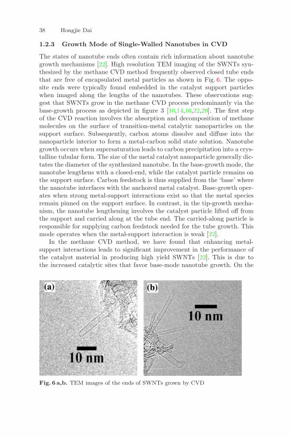
The states of nanotube ends often contain rich information about nanotubegrowth mechanisms [22]. High resolution TEM imaging of the SWNTs syn-thesized by the methane CVD method frequently observed closed tube endsthat are free of encapsulated metal particles as shown in Fig. 6. The oppo-site ends were typically found embedded in the catalyst support particleswhen imaged along the lengths of the nanotubes. These observations sug-gest that SWNTs grow in the methane CVD process predominantly via thebase-growth process as depicted in figure 3 [10,14,16,22,29]. The first stepof the CVD reaction involves the absorption and decomposition of methanemolecules on the surface of transition-metal catalytic nanoparticles on thesupport surface. Subsequently, carbon atoms dissolve and diffuse into thenanoparticle interior to form a metal-carbon solid state solution. Nanotubegrowth occurs when supersaturation leads to carbon precipitation into a crys-talline tubular form. The size of the metal catalyst nanoparticle generally dic-tates the diameter of the synthesized nanotube. In the base-growth mode, thenanotube lengthens with a closed-end, while the catalyst particle remains onthe support surface. Carbon feedstock is thus supplied from the ‘base’ wherethe nanotube interfaces with the anchored metal catalyst. Base-growth oper-ates when strong metal-support interactions exist so that the metal speciesremain pinned on the support surface. In contrast, in the tip-growth mecha-nism, the nanotube lengthening involves the catalyst particle lifted off fromthe support and carried along at the tube end. The carried-along particle isresponsible for supplying carbon feedstock needed for the tube growth. Thismode operates when the metal-support interaction is weak [22].
In the methane CVD method, we have found that enhancing metal-support interactions leads to significant improvement in the performance ofthe catalyst material in producing high yield SWNTs [22]. This is due tothe increased catalytic sites that favor base-mode nanotube growth. On the
Fig. 6 a,b. TEM images of the ends of SWNTs grown by CVD

Nanotube Growth and Characterization 39
other hand, catalysts with weak metal-support interactions lead to aggrega-tion of metal species and reduced nanotube yield and purity. Large metalparticles due to the aggregation often lead to the growth of multi-layeredgraphitic particles or defective multi-walled tube structures. Metal-supportinteractions are highly dependent on the type of support materials and thetype of metal precursor being used in preparing the catalyst [22].
1.3 Gas Phase Catalytic Growth
It has also been demonstrated that catalytic growth of SWNTs can be grownby reacting hydrocarbons or carbon monoxide with catalyst particles gener-ated in-situ. Cheng and coworkers reported a method that employs benzeneas the carbon feedstock, hydrogen as the carrier gas, and ferrocene as thecatalyst precursor for SWNT growth [30]. In this method, ferrocene is va-porized and carried into a reaction tube by benzene and hydrogen gases.The reaction tube is heated at 1100–1200C. The vaporized ferrocene de-composes in the reactor, which leads to the formation of iron particles thatcan catalyze the growth of SWNTs. With this approach however, amorphouscarbon generation could be a problem, as benzene pyrolysis is expected tobe significant at 1200C. Smalley and coworkers has developed a gas phasecatalytic process to grow bulk quantities of SWNTs [31]. The carbon feed-stock is carbon monoxide (CO) and the growth temperature is in the rangeof 800–1200C. Catalytic particles for SWNT growth are generated in-situby thermal decomposition of iron pentacarbonyl in a reactor heated to thehigh growth temperatures. Carbon monoxide provides the carbon feedstockfor the growth of nanotubes off the iron catalyst particles. CO is a very stablemolecule and does not produce unwanted amorphous carbonaceous materialat high temperatures. However, this also indicates that CO is not an efficientcarbon source for nanotube growth. To enhance the CO carbon feedstock,Smalley and coworkers have used high pressures of CO (up to 10 atm) tosignificantly speed up the disproportionation of CO molecules into carbon,and thus enhance the growth of SWNTs. The SWNTs produced this wayare as small as 0.7 nm in diameter, the same as that of a C60 molecule. Theauthors have also found that the yield of SWNTs can be increased by intro-ducing a small concentration of methane into their CO high pressure reactorat 1000–1100C growth temperatures. Methane provides a more efficient car-bon source than CO and does not undergo appreciable pyrolysis under theseconditions. The high pressure CO catalytic growth approach is promising forbulk production of single-walled carbon nanotubes.
2 Controlled Nanotube Growthby Chemical Vapor Deposition
Recent interest in CVD nanotube growth is also due to the idea that alignedand ordered nanotube structures can be grown on surfaces with control thatis not possible with arc-discharge or laser ablation techniques [23,32].

40 Hongjie Dai
2.1 Aligned Multi-Walled Nanotube Structures
Methods that have been developed to obtain aligned multi-walled nanotubesinclude CVD growth of nanotubes in the pores of mesoporous silica, an ap-proach developed by Xie’s group at the Chinese Academy of Science [33,34].The catalyst used in this case is iron oxide particles created in the poresof silica, the carbon feedstock is 9% acetylene in nitrogen at an overall 180torr pressure, and the growth temperature is 600C. Remarkably, nanotubeswith lengths up to millimeters are made (Fig. 7a) [34]. Ren has grown rel-atively large-diameter MWNTs forming oriented ‘forests’ (Fig. 7b) on glasssubstrates using a plasma assisted CVD method with nickel as the catalystand acetylene as the carbon feedstock around 660C [35].
Our group has been devising growth strategies for ordered multi-walledand single-walled nanotube architectures by CVD on catalytically patternedsubstrates [23,32]. We have found that multi-walled nanotubes can self-assem-ble into aligned structures as they grow, and the driving force for self-align-ment is the Van der Waals interactions between nanotubes [36]. The growthapproach involves catalyst patterning and rational design of the substrateto enhance catalyst-substrate interactions and control the catalyst particle
Fig. 7. Aligned multi-walled nano-tubes grown by CVD methods.(a) An ultra-long aligned nanotubebundle (courtesy of S. Xie). (b) Anoriented MWNT forest grown onglass substrate (courtesy of Z. Ren)
Nanotube Growth and Characterization 41
size. Porous silicon is found to be an ideal substrate for this approach andcan be obtained by electrochemical etching of n-type silicon wafers in hy-drofluoric acid/methanol solutions. The resulting substrate consisted of athin nanoporous layer (pore size ∼ 3 nm) on top of a macroporous layer (withsubmicron pores). Squared catalyst patterns on the porous silicon substrateare obtained by evaporating a 5 nm thick iron film through a shadow maskcontaining square openings. CVD growth with the substrate is carried outat 700C under an ethylene flow of 1000 mL/min for 15 to 60min. Figure 8shows SEM images of regularly positioned arrays of nanotube towers grownfrom patterned iron squares on a porous silicon substrates. The nanotubetowers exhibit very sharp edges and corners with no nanotubes branchingaway from the blocks. The high resolution SEM image (Fig. 8c) reveals thatthe MWNTs (Fig. 8c inset) within each block are well aligned along the direc-tion perpendicular to the substrate surface. The length of the nanotubes andthus the height of the towers can be controlled in the range of 10–240µm byvarying the CVD reaction time. The width of the towers is controlled by thesize of the openings in the shallow mask. The smallest self-oriented nanotubetowers synthesized by this method are 2µm× 2µm.
The mechanism of nanotube self-orientation involves the nanotube base-growth mode [36]. Since the nanoporous layer on the porous silicon substrateserves as an excellent catalyst support, the iron catalyst nanoparticles formedon the nanoporous layer interact strongly with the substrate and remainpinned on the surface. During CVD growth, the outermost walls of nano-tubes interact with their neighbors via van der Waals forces to form a rigidbundle, which allows the nanotubes to grow perpendicular to the substrate(Fig. 8d). The porous silicon substrates exhibit important advantages overplain silicon substrates in the synthesis of self-aligned nanotubes. Growth onsubstrates containing both porous silicon and plain silicon portions finds thatnanotubes grow at a higher rate (in terms of length/min) on porous siliconthan on plain silicon. This suggests that ethylene molecules can permeatethrough the macroporous silicon layer (Fig. 8d) and thus efficiently feed thegrowth of nanotubes within the towers. The nanotubes grown on poroussilicon substrates have diameters in a relatively narrow range since cata-lyst nanoparticles with a narrow size distribution are formed on the poroussupporting surface, and the metal-support interactions prevent the catalyticmetal particles from sintering at elevated temperatures during CVD.
2.2 Directed Growth of Single-Walled Nanotubes
Ordered, single-walled nanotube structures can be directly grown by methaneCVD on catalytically patterned substrates. A method has been devised togrow suspended SWNT networks with directionality on substrates contain-ing lithographically patterned silicon pillars [25,37]. Contact printing is usedto transfer catalyst materials onto the tops of pillars selectively. CVD of

42 Hongjie Dai
Fig. 8. Self-oriented MWNT arrays grown by CVD on a catalytically patternedporous silicon substrate. (a) SEM image of tower structures consisted of alignednanotubes. (b) SEM image of the side view of the towers. (c) A high magnificationSEM image showing aligned nanotubes in a tower. Inset: TEM image showing twoMWNTs bundling together. (d) Schematic diagram of the growth process
methane using the substrates leads to suspended SWNTs forming nearly or-dered networks with the nanotube orientations directed by the pattern of thepillars (Fig. 9).
The growth approach starts with developing a liquid-phase catalyst pre-cursor material that has the advantage over solid-state supported catalysts inallowing the formation of uniform catalyst layers and for large-scale catalyticpatterning on surfaces [25,37]. The precursor material consists of a triblockcopolymer, aluminum, iron and molybdenum chlorides in mixed ethanol andbutanol solvents. The aluminum chloride provides an oxide framework whenoxidized by hydrolysis and calcination in air. The triblock copolymer directsthe structure of the oxide framework and leads to a porous catalyst structureupon calcination. The iron chloride can lead to catalytic particles needed forthe growth of SWNTs in methane CVD. The catalyst precursor material isfirst spun into a thin film on a poly-dimethyl siloxane (PDMS) stamp, fol-lowed by contact-printing to transfer the catalyst precursor selectively onto

Nanotube Growth and Characterization 43
Fig. 9. Directed growth of suspended SWNT. (a) A nanotube power-line structure.(b) A square of nanotubes. (c) An extensive network of suspended SWNTs
the tops of pillars pre-fabricated on a silicon substrate. The stamped sub-strate is calcined and then used in CVD growth.
Remarkably, the SWNTs grown from the pillar tops tend to direct frompillar to pillar. Well-directed SWNT bridges are obtained in an area of thesubstrate containing isolated rows of pillars as shown in Fig. 9a, where sus-pended tubes forming a power-line like structure can be seen. In an areacontaining towers in a square configuration, a square of suspended nanotubebridges is obtained (Fig. 9b). Suspended SWNTs networks extending a largearea of the substrate are also formed (Fig. 9c). Clearly, the directions of theSWNTs are determined by the pattern of the elevated structures on the sub-strate. Very few nanotubes are seen to extend from pillars and rest on thebottom surface of the substrate.
The self-directed growth can be understood by considering the SWNTgrowth process on the designed substrates [25]. Nanotubes are nucleated onlyon the tower-tops since the catalytic stamping method does not place any cat-alyst materials on the substrate below. As the SWNTs lengthen, the methaneflow keeps the nanotubes floating and waving in the ‘wind’ since the flow ve-locity near the bottom surface is substantially lower than that at the level ofthe tower-tops. This prevents the SWNTs from being caught by the bottomsurface. The nearby towers on the other hand provide fixation points for thegrowing tubes. If the waving SWNTs contact adjacent towers, the tube-towervan der Waals interactions will catch the nanotubes and hold them aloft.
44 Hongjie Dai
Growing defect-free nanotubes continuously to macroscopic lengths hasbeen a challenging task. In general, continuous nanotube growth requiresthe catalytic sites for SWNTs remaining active indefinitely. Also, the carbonfeedstock must be able to reach and feed into the catalytic sites in a continu-ous fashion. For CVD growth approaches, this means that catalyst materialswith high surface areas and open pore structures can facilitate the growth oflong nanotubes, as discussed earlier.
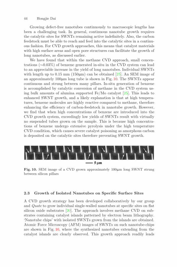
We have found that within the methane CVD approach, small concen-trations (∼0.03%) of benzene generated in-situ in the CVD system can leadto an appreciable increase in the yield of long nanotubes. Individual SWNTswith length up to 0.15 mm (150µm) can be obtained [25]. An SEM image ofan approximately 100µm long tube is shown in Fig. 10. The SWNTs appearcontinuous and strung between many pillars. In-situ generation of benzeneis accomplished by catalytic conversion of methane in the CVD system us-ing bulk amounts of alumina supported Fe/Mo catalyst [25]. This leads toenhanced SWNT growth, and a likely explanation is that at high tempera-tures, benzene molecules are highly reactive compared to methane, thereforeenhancing the efficiency of carbon-feedstock in nanotube growth. However,we find that when high concentrations of benzene are introduced into theCVD growth system, exceedingly low yields of SWNTs result with virtuallyno suspended tubes grown on the sample. This is because high concentra-tions of benzene undergo extensive pyrolysis under the high temperatureCVD condition, which causes severe catalyst poisoning as amorphous carbonis deposited on the catalytic sites therefore preventing SWNT growth.
Fig. 10. SEM image of a CVD grown approximately 100m long SWNT strungbetween silicon pillars
2.3 Growth of Isolated Nanotubes on Specific Surface Sites
A CVD growth strategy has been developed collaboratively by our groupand Quate to grow individual single-walled nanotubes at specific sites on flatsilicon oxide substrates [20]. The approach involves methane CVD on sub-strates containing catalyst islands patterned by electron beam lithography.‘Nanotube chips’ with isolated SWNTs grown from the islands are obtained.Atomic Force Microscopy (AFM) images of SWNTs on such nanotube-chipsare shown in Fig. 10, where the synthesized nanotubes extending from thecatalyst islands are clearly observed. This growth approach readily leads

Nanotube Growth and Characterization 45
to SWNTs originating from well controlled surface sites, and have enabledus to develop a controlled method to integrate nanotubes into addressablestructures for the purpose of elucidating their fundamental properties andbuilding devices with interesting electrical, electromechanical and chemicalfunctions [23,38,39,40,41,42,43,44].
2.4 From Growth to Molecular-Wire Devices
Integrating individual nanotubes into addressable structures is importantto the characterization of nanotubes. It is necessary to investigate individ-ual tubes because the properties of nanotubes are highly sensitive to theirstructural parameters, including chirality and diameter. Currently, all of thegrowth methods yield inhomogeneous materials containing nanotubes withvarious chiralities. Therefore, measurements of ensembles of nanotubes canonly reveal their bulk averaged properties.
2.4.1 Electrical Properties of Individual Nanotubes
Previous approaches to individual SWNT electrical devices include randomlydepositing SWNTs from liquid suspensions onto pre-defined electrodes [4,45],or onto a flat substrate followed by locating nanotubes and patterning elec-trodes [46,47,48,49]. We have demonstrated that controlled nanotube growthstrategies open up new routes to individually addressable nanotubes. TheSWNTs grown from specific sites on substrates can be reliably contacted byelectrodes (Figs. 11c, 12a) and characterized [38]. Metal electrodes are placedonto the two ends of a nanotube via lithography patterning and electronbeam evaporation. Detailed procedure for contacting a SWNT can be foundin [38].
The formation of low ohmic contacts with SWNTs is critical to elucidatingtheir intrinsic electrical properties [40] and building devices with advancedcharacteristics. This is accomplished by our controlled approach of growingand contacting nanotubes. We found that titanium metal contacts give riseto the lowest contact resistance compared to other metals. Metallic SWNTsthat are several microns long typically exhibit two-terminal resistance onthe order of tens to hundreds of kilo-ohms. The lowest single-tube resistancemeasured with our individual metallic SWNT is ∼ 12 k Ω (Fig. 12b). The lowcontact resistance achieved in our system can be attributed to several fac-tors. The first is that our method allows the two metal electrodes to contactthe two ends of a nanotube. Broken translational symmetry at the nanotubeends could be responsible for the strong electrical coupling between the tubeand metal [50]. Secondly, titanium–carbon (carbide) bond formation at themetal–tube interface may have occurred during the electron-beam evapora-tion process. This is based on our result that titanium yields lower contactresistance than other metals, including aluminum and gold, and the fact that

46 Hongjie Dai
Fig. 11. Growth of single-walled nanotubes on controlled surface sites and deviceintegration. (a) An atomic force microscopy image of SWNTs grown from patternedcatalyst dots (while spots). (b) AFM image of a SWNT grown between two catalystsites (white corners). (c) AFM image of a SWNT grown from a catalyst island andcontacted by metal electrodes
aluminum and gold do not form strong bonding with carbon and stable car-bide compounds.
For individual semiconducting SWNTs grown on surfaces, relatively lowresistance devices on the order of hundreds of kilo-ohms can be made byour approach [40]. These nanotubes exhibit p-type transistor behavior atroom temperature as their conductance can be dramatically changed bygate voltages (Fig. 12c). This property is consistent with the initial observa-tion made with high resistance samples (several mega-ohms) by Dekker [51]and by Avouris’ group [52]. The transconductance (ratio of current changeover gate-voltage change) of our semiconducting tube samples can be up to∼200nA/V [40] which is two orders of magnitude higher than that measuredwith earlier samples. The high transconductance is a direct result of the rela-tively low resistance of our semiconducting SWNT samples, as high currentscan be transported through the system at relatively low bias voltages. Thisresult should not be underestimated, given the importance of high transcon-ductance and voltage gain to transistors. Nevertheless, future work is neededin order to create semiconducting SWNT devices with transconductance andvoltage gains that match existing silicon devices.

Nanotube Growth and Characterization 47
Fig. 12. Electrical properties ofindividual single-walled carbonnanotubes. (a) AFM image ofan individual single-walled nano-tube contacted by two metal elec-trode. The length of the nano-tube between electrodes is ∼ 3m.(b) Temperature dependent re-sistance of a metallic SWNT.(c) Current (I) vs. voltage (V)characteristics of a semiconduct-ing nanotube under various gate-voltages (Vg)
2.4.2 Nanotube Electromechanical Properties and Devices
Controlled growth of nanotubes on surfaces combined with microfabricationapproaches allows the construction of novel nanotube devices for new types ofstudies. For instance, the question of how mechanical deformation affects theelectrical properties of carbon nanotubes has been intriguing [53,54,55,56,57],and is important to potential applications of nanotubes as building blocksfor nanoscale electro-mechanical devices. To address this question experi-mentally, it will be desired to obtains suspended nanotubes that can be ma-nipulated mechanically and at the same time addressed electrically. To thisend, we have grown individual SWNTs from patterned catalyst sites across
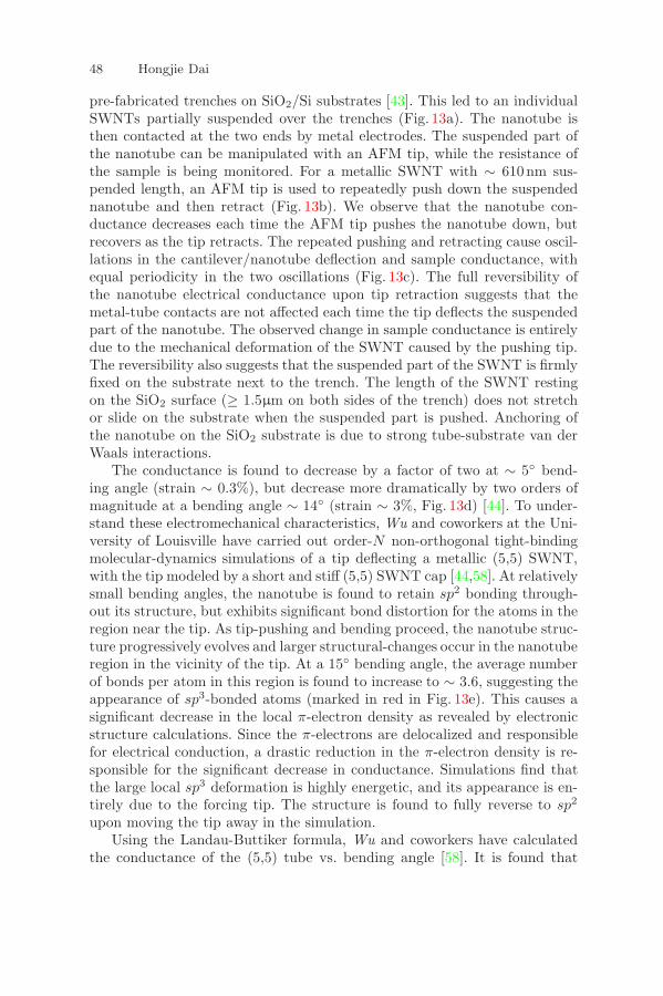
48 Hongjie Dai
pre-fabricated trenches on SiO2/Si substrates [43]. This led to an individualSWNTs partially suspended over the trenches (Fig. 13a). The nanotube isthen contacted at the two ends by metal electrodes. The suspended part ofthe nanotube can be manipulated with an AFM tip, while the resistance ofthe sample is being monitored. For a metallic SWNT with ∼ 610nm sus-pended length, an AFM tip is used to repeatedly push down the suspendednanotube and then retract (Fig. 13b). We observe that the nanotube con-ductance decreases each time the AFM tip pushes the nanotube down, butrecovers as the tip retracts. The repeated pushing and retracting cause oscil-lations in the cantilever/nanotube deflection and sample conductance, withequal periodicity in the two oscillations (Fig. 13c). The full reversibility ofthe nanotube electrical conductance upon tip retraction suggests that themetal-tube contacts are not affected each time the tip deflects the suspendedpart of the nanotube. The observed change in sample conductance is entirelydue to the mechanical deformation of the SWNT caused by the pushing tip.The reversibility also suggests that the suspended part of the SWNT is firmlyfixed on the substrate next to the trench. The length of the SWNT restingon the SiO2 surface (≥ 1.5µm on both sides of the trench) does not stretchor slide on the substrate when the suspended part is pushed. Anchoring ofthe nanotube on the SiO2 substrate is due to strong tube-substrate van derWaals interactions.
The conductance is found to decrease by a factor of two at ∼ 5 bend-ing angle (strain ∼ 0.3%), but decrease more dramatically by two orders ofmagnitude at a bending angle ∼ 14 (strain ∼ 3%, Fig. 13d) [44]. To under-stand these electromechanical characteristics, Wu and coworkers at the Uni-versity of Louisville have carried out order-N non-orthogonal tight-bindingmolecular-dynamics simulations of a tip deflecting a metallic (5,5) SWNT,with the tip modeled by a short and stiff (5,5) SWNT cap [44,58]. At relativelysmall bending angles, the nanotube is found to retain sp2 bonding through-out its structure, but exhibits significant bond distortion for the atoms in theregion near the tip. As tip-pushing and bending proceed, the nanotube struc-ture progressively evolves and larger structural-changes occur in the nanotuberegion in the vicinity of the tip. At a 15 bending angle, the average numberof bonds per atom in this region is found to increase to ∼ 3.6, suggesting theappearance of sp3-bonded atoms (marked in red in Fig. 13e). This causes asignificant decrease in the local π-electron density as revealed by electronicstructure calculations. Since the π-electrons are delocalized and responsiblefor electrical conduction, a drastic reduction in the π-electron density is re-sponsible for the significant decrease in conductance. Simulations find thatthe large local sp3 deformation is highly energetic, and its appearance is en-tirely due to the forcing tip. The structure is found to fully reverse to sp2
upon moving the tip away in the simulation.Using the Landau-Buttiker formula, Wu and coworkers have calculated
the conductance of the (5,5) tube vs. bending angle [58]. It is found that

Nanotube Growth and Characterization 49
Fig. 13. Electromechanical characteristics of suspended nanotubes. (a) AFM imageof a SWNT with a ∼ 605 nm long suspension over a trench. The bright spotsaround the suspended tube part are caused by tube touching and sticking to theside of the pyramidal scanning tip. (b) A schematic view of the electromechanicalmeasurement setup. (c) Cantilever deflection (∆Zc, upper graph) and nanotubeelectrical conductance (G, lower graph) evolution during repeated cycles of pushingthe suspended SWNT and retracting. (d) Electrical conductance (G) of the SWNTsample vs. bending angle (θ). (e) Simulated atomic configurations of a (5,5) SWNTpushed to a 15 degrees bending angle by an AFM tip
at relatively small bending angles, the conductance of the SWNT exhibitsappreciable decrease, but the decrease is relatively gradual. The conduc-tance decrease is caused by the relatively large C–C bond distortions in thenanotube region near the tip. The decrease is gradual because the overallnanotube structure remains in the sp2 state. At large bending angles, the

50 Hongjie Dai
nanotube conductance decreases dramatically, as sp3 bonding sets into thenanotube structure. These results agree qualitatively with experimental dataand thus provide a detailed rationale to the observed nanotube electrome-chanical characteristics. The combined experimental and theoretical studyleads to an in-depth understanding of nanotube electromechanical proper-ties, and suggests that SWNTs could serve as reversible electro-mechanicaltransducers that are potentially useful for nano-electro-mechanical devices.
The electro-mechanical characteristics are elucidated when the nanotubedeformation is caused by a manipulating local probe. This should be dis-tinguished from previous theoretical considerations of ‘smoothly’ bent nano-tubes. Nanotube bending in most of the earlier investigations is modeled byholding the ends of a nanotube such that the nanotube is at a certain bendingconfiguration [54,55,56]. In most of the cases studied, the nanotube remainsin the sp2 state with only small bond distortions throughout the structure.Therefore, the nanotube conductance has been found to be little changed(< 10 fold) under bending angles up to 20. Nevertheless, Rochefort et al.did find that at larger bending angles (e.g. θ=45), the electrical conduc-tance of a metallic (6,6) SWNT is lowered up to 10-fold [55,56]. The physicsstudied in our case should be applicable to SWNTs containing large localdeformations caused by other forces. For instance, if a highly kinked SWNTstabilized by van der Waals forces on a substrate develops sp3 type of bondingcharacteristics at the kink, the electrical conductance should be significantlyreduced compared to a straight tube.
3 Conclusions
We have presented an overview of various growth methods for multi-walledand single-walled carbon nanotubes. It is shown that chemical vapor de-position approaches are highly promising for producing large quantities ofhigh quality nanotube materials at large scales. Controlling nanotube growthwith CVD strategies has led to organized nanowires that can be readily in-tegrated into addressable structures useful for fundamental characterizationand potential applications. It can be envisioned that in a foreseeable future,controlled growth will yield nanotube architectures used as key componentsin next generations of electronic, chemical, mechanical and electromechanicaldevices.
It is fair to say that progress in nanotube research has been built uponthe successes in materials synthesis. This trend shall continue. It is perhapsan ultimate goal for growth to gain control over the nanotube chirality anddiameter, and be able to direct the growth of a semiconducting or metallicnanowire from and to any desired sites. Such control will require significantfuture effort, and once successful, is likely to bring about revolutionary op-portunities in nanoscale science and technology.

Nanotube Growth and Characterization 51
Acknowledgements
The work carried out at Stanford were done by J. Kong, N. Franklin, T.Tombler, C. Zhou, R. Chen, A. Cassell, M. Chapline, E. Chan and T. Soh.We thank Professors C. Quate, S. Fan, S. Y. Wu, C. Marcus and Dr. J. Hanfor fruitful collaborations. This work was supported financially by NationalScience Foundation, DARPA/ONR, a Packard Fellowship, a Terman Fel-lowship, Semiconductor Research Corporation/Motorola Co., SemiconductorResearch Corporation/Semetech., the National Nanofabrication Users Net-work at Stanford, Stanford Center for Materials Research, the Camile Henry-Dreyfus Foundation and the American Chemical Society.
References
1. S. Iijima, Nature 354, 56–58 (1991) 292. S. Iijima, T. Ichihashi, Nature 363, 603–605 (1993) 293. M. S. Dresselhaus, G. Dresselhaus, P. C. Eklund, Science of Fullerenes and
Carbon Nanotubes (Academic, San Diego 1996) 294. C. Dekker, Phys. Today 52, 22–28 (1999) 29, 455. T. W. Ebbesen, P. M. Ajayan, Nature 358, 220–222 (1992) 316. D. S. Bethune, C. H. Kiang, M. DeVries, G. Gorman, R. Savoy, J. Vazquez,
R. Beyers, Nature 363, 605–607 (1993) 317. A. Thess, R. Lee, P. Nikolaev, H. J. Dai, P. Petit, J. Robert, C. H. Xu, Y. H. Lee,
S. G. Kim, A. G. Rinzler, D. T. Colbert, G. E. Scuseria, D. Tomanek, J. E. Fis-cher, R. E. Smalley, Science 273, 483–487 (1996) 31
8. C. Journet, W. K. Maser, P. Bernier, A. Loiseau, M. L. Delachapelle, S. Lefrant,P. Deniard, R. Lee, J. E. Fischer, Nature 388, 756–758 (1997) 31
9. J. Liu, A. G. Rinzler, H. Dai, J. H. Hafner, R. K. Bradley, P. J. Boul, A.Lu, T. Iverson, K. Shelimov, C. B. Huffman, F. Rodriguez-Macias, Y.-S. Shon,T. R. Lee, D. T. Colbert, R. E. Smalley, Science 280, 1253–1256 (1998) 31
10. G. G. Tibbetts, J Cryst. Growth 66, 632–638 (1984) 32, 3811. G. G. Tibbetts, Carbon 27, 745-747 (1989) 3212. G. G. Tibbetts: Filaments and Composites, in Carbon Fibers (Kluwer Aca-
demic, Amsterdam 1990) pp. 73–94 3213. G. G. Tibbetts, J. Cryst. Growth 73, 431–438 (1985) 3214. G. G. Tibbetts, M. G. Devour, E. J. Rodda, Carbon 25, 367–375 (1987) 32,
3815. R. T. K. Baker, Physics and Chemistry of Carbon, Vol.14, P. Walker,
P. Thrower, (Eds.) (Dekker, New York 1978) pp. 83–165 3216. R. T. K. Baker, Carbon 27, 315–323 (1989) 32, 3817. R. T. K. Baker, L. L. Murrell, (Eds.), Novel Materials in Heterogeneous Catal-
ysis (Washington, DC 1990) 3218. H. G. Tennent, Hyperion Catalysis International, Inc., US patent no. 4663230,
USA, (1987) 3219. C. E. Snyder, W. H. Mandeville, H. G. Tennent, L. K. Truesdale, Hyperion
Catalysis International, US patent, (1989) 3220. J. Kong, A. M. Cassell, H. Dai, Chem. Phys. Lett. 292, 567-574 (1998) 34, 44

52 Hongjie Dai
21. J. Kong, H. Soh, A. Cassell, C. F. Quate, H. Dai, Nature 395, 878–879 (1998)34
22. A. Cassell, J. Raymakers, J. Kong, H. Dai, J. Phys. Chem. 103, 6484–6492(1999) 34, 35, 38, 39
23. H. Dai, J. Kong, C. Zhou, N. Franklin, T. Tombler, A. Cassell, S. Fan, M. Chap-line, J. Phys. Chem. 103, 11246–11255 (1999) 34, 39, 40, 45
24. J. Hafner, M. Bronikowski, B. Azamian, P. Nikolaev, D. Colbert, R. Smalley,Chem. Phys. Lett. 296, 195–202 (1998) 35
25. N. Franklin, H. Dai, Adv. Mater. 12, 890 (2000) 36, 41, 42, 43, 4426. M. Su, B.Zheng, J. Liu, Chem. Phys. Lett. 322, 321-326 (2000) 3727. E. Flahaut, A. Govindaraj, A. Peigney, C. Laurent, C. N. Rao, Chem. Phys.
Lett. 300, 236–242 (1999) 3728. J.-F. Colomer, C. Stephan, S. Lefrant, G. V. Tendeloo, I. Willems, Z. Kanya,
A. Fonseca, C. Laurent, J. B.Nagy, Chem. Phys. Lett. 317, 83–89 (2000) 3729. S. Amelinckx, X. B. Zhang, D. Bernaerts, X. F. Zhang, V. Ivanov, J. B. Nagy,
Science 265, 635–639 (1994) 3830. H. Cheng, F. Li, G. Su, H. Pan, M. Dresselhaus, Appl. Phys. Lett. 72, 3282–
3284 (1998) 3931. P. Nikolaev, M. J. Bronikowski, R. K. Bradley, F. Rohmund, D. T. Colbert,
K. A. Smith, R. E. Smalley, Chem. Phys. Lett. 313, 91–97 (1999) 3932. H. Dai, Phys. World (2000) 39, 4033. W. Z. Li, S. S. Xie, L. X. Qian, B. H. Chang, B. S. Zou, W. Y. Zhou, R. A. Zhao,
G. Wang, Science 274, 1701–1703 (1996) 4034. Z. Pan, S. S.Xie, B. Chang, C. Wang, Nature 394, 631–632 (1998) 4035. Z. F. Ren, Z. P. Huang, J. W. Xu, J. H. Wang, Science 282, 1105–1107 (1998)
4036. S. Fan, M. Chapline, N. Franklin, T. Tombler, A. Cassell, H. Dai, Science 283,
512–514 (1999) 40, 4137. A. Cassell, N. Franklin, T. Tombler, E. Chan, J. Han, H. Dai, J. Am. Chem.
Soc. 121, 7975-7976 (1999) 41, 4238. H. Soh, C. Quate, A. Morpurgo, C. Marcus, J. Kong, H. Dai, Appl. Phys. Lett.
75, 627–629 (1999) 4539. A. Morpurgo, J. Kong, C. Marcus, H. Dai, Science 286, 263-265 (1999) 4540. C. Zhou, J. Kong, H. Dai, Appl. Phys. Lett. 76, 1597–1599 (1999) 45, 4641. J. Kong, N. Franklin, C. Zhou, M. Chapline, S. Peng, K. Cho, H. Dai, Science
287, 622-625 (2000) 4542. C. Zhou, J. Kong, H. Dai, Phys. Rev. Lett. 84, 5604 (2000) 4543. T. Tombler, C. Zhou, J. Kong, H. Dai, Appl. Phys. Lett. 76, 2412–2414 (2000)
45, 4844. T. Tombler, C. Zhou, L. Alexeyev, J. Kong, H. Dai, L. Liu, C. Jayanthi,
M. Tang, S. Y. Wu, Nature 405, 769 (2000) 45, 4845. S. J. Tans, M. H. Devoret, H. Dai, A. Thess, R. E. Smalley, L. J. Geerligs,
C. Dekker, Nature 386, 474-477 (1997) 4546. M. Bockrath, D. H. Cobden, P. L. McEuen, N. G. Chopra, A. Zettl, A. Thess,
R. E. Smalley, Science 275, 1922-1925 (1997) 4547. D. H. Cobden, M. Bockrath, N. G. Chopra, A. Zettl, P. McEuen, A. Rinzler,
R. E. Smalley, Phys. Rev. Lett. 81, 681-684 (1998) 4548. M. Bockrath, D. Cobden, J. Lu, A. Rinzler, R. Smalley, L. Balents, P. McEuen,
Nature 397, 598–601 (1999) 45

Nanotube Growth and Characterization 53
49. J. Nygard, D. H. Cobden, M. Bockrath, P. L. McEuen, P. E. Lindelof, Appl.Phys. A 69, 297–304 (1999) 45
50. J. Tersoff, Appl. Phys. Lett. 74, 2122–2124 (1999) 4551. S. Tans, A. Verschueren, C. Dekker, Nature 393, 49–52 (1998) 4652. R. Martel, T. Schmidt, H. R. Shea, T. Hertel, Ph. Avouris, Appl. Phys. Lett.
73, 2447–2449 (1998) 4653. C. L. Kane, E. J. Mele, Phys. Rev. Lett. 78, 1932–1935 (1997) 4754. M. Nardelli, J. Bernholc, Phys. Rev. B 60, R16338–16341 (1998) 47, 5055. A. Rochefort, D. Salahub, Ph. Avouris, Chem. Phys. Lett. 297, 45–50 (1998)
47, 5056. A. Rochefort, F. Lesage, D. Salhub, Ph. Avouris, Phys. Rev. B 60, 13824–13830
(1999) 47, 5057. S. Paulson, M. Falvo, N. Snider, A. Helser, T. Hudson, A. Seeger, R. Taylor,
R. Superfine, S. Washburn, Appl. Phys. Lett. 75, 2936–2938 (1999) 4758. L. Liu, C. Jayanthi, M. Tang, S. Y. Wu, T. Tombler, C. Zhou, L. Alexeyev,
J. Kong, H. Dai, Phys. Rev. Lett. 84, 4950 (2000). 48