nanostructured antireflection (ar) coatings for
TRANSCRIPT

In : Comprehensive Guide for Nanocoatings Technology. Vol. 4 ISBN. 978- 1-63482-648-8 Editor: Mahmood A[iofkhazraei © 20 [5 Nova Science Publishers, Inc .
Chapler 8
The lken~ for 11,i5 PDF is unlimiled CXCCpl lhal '00 pan oflhis digital do<;unlem ,nal" he reprodue<:d. slored in a ", .. ie,·al ,)', Iem 0' lrallSmiued con"tIC.d.lll" in am' fonn 0' bl' an,' means. The publisher has w;en reasonable care in Ihe preparalion Ofll' i5 digilal documcn .. bUI ,nakcs '00 exp",ssed 0' implied "armml" of any kind and aSSll'tICS lIO fI'S"'.l1lsibilil)' for anI" errors 0' omissions. No liabililY is aSSll'tICd for hleidcmal o. cOllSCq,ocmi.1 da,nages in conneclion "ill, o. arising OUI of infonnalion comained llereh'. This digilal docu'tICm i5 sold "ilh lhe deaf understa"ding Ihal Ihe p,oblishe';s lIOl engaged;n rendering legal. ,nedkal 0' anI" olhe. professional services
NANOSTRUCTURED ANTIREFLECTION (AR)
COATINGS FOR OPTOELECTRONIC ApPLICATIONS
AsllOk K. Sooll, Roger E. Welser', Gopal G. Petlturaja ' ,
Adalll W. Sood', Yaslt R. PuTi', E. Fred Scltuberr, Pradeep Halda,.',
Nibir K. Dllllr4, Dennis L. PolI,/ and Priyalal Wijewarnasuriya6
lMagnolia Opti ca l Techno logies [nc ., Woburn, MA
20epartment of ECSE and Physics, Rensselaer Polytech nic In stitute , Troy, NY
)Co ll eges o f Nan oscale Science and Engi neering
SU NY Polytechnic In stitute, Albany, N Y
40 efen se Advanced Project Agency, Arlington, VA
5College o f Science and Engi neering, Un ivers ity of Minnesota, Min neapo lis, MN
6 Army Research Labs, Adelphi , MO
ARSTRACT
Thi s Chapter will cover recent advances in nanostructured based detector technology i.e., materials and device fo r a variety of optoelectronic detection applications. The material used in this chapter will include the published work in a variety of jouma[s and research performed under various programs in the US. The authors have many years of experience working on a variety of nanotec hnologies that inel ude a variety of se miconductors and other advanced materials for optical applications.
One of the critiea[ tec hnologies that will enhance the electro-optic/infrared (EO/IR) sensor performance is the development of hi gh quality nanostructme based antirefl ection coating. We will discuss our results on the high performance nanostructme antirefl ection coatings using TiO l and SiOl graded-index nanorods deposited by oblique-ang[e deposition.
In thi s chapter, we wil l show that obliq ue angle nanowires and nanorods growth of SiOl and TiO l otTer an innovati ve approach for developing high qual ity anti -refection coatings (A RC) for usc on next generation sensors for both defense and commercial applications.

184 Ashok K. Sood, Roger E. Weiser, Gopal G. Pethuraja et al.
I. I NTRO DUCTiO N
El ectro-optic/ infrared (EO/IR) sensors operate in the optical radiation portion of the electromagnet ic (EM ) spectrum. These include Ultraviolet (UV), Visible, near-infrared (N IR) and long wave infrared (LWIR) Sensors . These sensors are being developed for use in a variety of defense and commerc ial applications [1 --6]. Current Visible-N1 R focal plane arrays (FAP) use InGaAs and SiGe that operate in 0.4 to 1.7 micron band [2].
Simil arly, mid-wave infrared (MW IR) Sensors use inSb or HgCdTe based FPA' s thai are sens itive in 3-5 micron region [3 , 4]. LWIR band uses either HgCdTe, strained-layer super lattice (S LS) structures, or Si-MEMS based Microbolorneters [5 , 6}. To further enhance the performance of EOII R sensors, radiation hardened antireflection (A R) coatings have been studied in us ing multilayer coatings on Silicon and CdTe substrates for MW IR and LWIR applications [7].
These systems have been made possible, by substantial investment by Department of Defense (000) and National Aeronauti cs and Space Administration (N ASA) in the critical technologies for short-wave infrared (SW IR), MW IR and LWIR Focal Pl ane Array and Sensor Packaging Technologies . These investments have provided the necessary building blocks for the infrared (l R) sensors that are being deployed in the field . These efforts have addressed the performance enhancements and producibility of the key optical components . Table 1.1 list the various semiconductors used in the EO/IR sensor and its refractive index .
The semiconductors used in EOIIR sensors have high refracti ve index, leading to a signi ficant amount of reflection from the top surface . This wi ll reduce the light throughput to the sensor and also the field of view. Hence, all of these EOII R nanosensor technologies will benefit from the development of advanced antireflection (A R) coatings that min imize reflection losses over a wide range of wavelengths and incident angles .
Table 1.1. Refractive ind ex of semiconductors used in EO/IR senso rs
Scnsor type Scmiconductors Refractive index Visiblc-NIR sensors InGaAs, SiGc 3.71 , 3.69
Mid-wavc infrared sensors InSb, HgCdTc 4.42, 3.69 Long-wave infrarcd scnsors HgCdTe, Si MEMS 3.69, 3.69
The use of Obl ique Angle Nanowires for developing the critical technologies that will allow mi nimizing the reflection loss has recently been studied by Schubert et aI., at RPI and reported in a paper in Nature [8}. Their work has explored the possibi lity of using nanowires grown by oblique angle deposition technique. Their initial investigation was based on studying the work by Lord Rayleigh that graded -refractive index layers have broadband antireflection characteristics.
Graded-index coatings wi th different index profiles have been investigated for broadband antireflection properties, particularly with ai r as the ambient medium. However, because of the unavail ability of optical materials with very low refractive ind ices that closely match the refractive index of air, such high quality broadband antireflection coatings have not been real izable.

Nanostructured Antireflection (AR) Coatings . 185
2. NA NOWIR E A NTI REFLECTIO N (A R ) COATING
Reduc ing optical reflection from surfaces is important to many applications in optics. This is commonly achieved through coating, or texturing, the surface of interest. Numerous applications involving dielectric or semiconducting materials use the light that is transmitted through the material ' s surface.
Examples of such application are optical lenses, windows, photovohaic devices, and photodetectors. Glass (amorpho us SiOl ) is one such dielectric material widely used in a variety of optical applications e.g., lenses, windows, and as a cover or encaps ulation for semiconductor optoelectronic devices .
Glass is completely transparent for wavelengths longer than 400 nm. However, due to Fresnel reflection it reflects about 4% of the incident light from its surface (- 8% from two surfaces). This refl ection is undes irable in many applications as it can degrade the efficiency of the underlying device (e,g., the effic iency of a solar photovoltaic cell), reduce signal-tonoise ratio (e.g., in a photodetector), and cause glare (e,g., from LC D screens, computer monitors, and televisions).
For such applicat ions, it is important not on ly to reduce reflectance but also to improve the transmittance through the surface. This requires that the coating material be nonabsorbi ng and the coating surface be specular.
Conventionally, a si ngle-layer coating with optical thickness equal to one quarter of the wavelength (}J4) of interest has been used as an AR coating. Ideally such si ngle-layer}J4 AR coating should have a refractive index, " )) 4 as given by Eq. (1) [9].
( I )
Often due to unavailabi lity of materials with the desi red, exact val ue of the refractive index, the performance of such }J4 AR coatings deviates from the optimum. This is especially the case for low-index substrates, such as glass. An ideal single-layer}J4 AR coating on glass surface in an air ambient would require a material with refractive index of (1 .46)112 :::0 1.2.
There is no conventional inorganic material that has such a low refractive index . Also, fundamentally, these single-layer }J4 AR coatings can minimize reflection only for one specific wavelength at normal incidence and they are inherently unable to exhibit spectrally broadband reduction in reflectance over wide range of angles-o f-incidence.
To accomplish broadband antireflection, various anti reflection mechanisms explored using wide verity of materials, process methodology and structure . Table 2.1 presents various antireflection technologies that have been developed .
In 1880, Lord Rayle igh mathemat ically demonstrated that graded-refractive-i ndex layers have broadband antireflection properties . Mul ti-layer stacks of materials with different refractive ind ices have been used in order to achieve broadband reduction in reflection [10). [11]. Anti-reflection (AR) coatings with specular surface made of multiple discrete layers of non-absorbi ng materials can exploit thin film interfe rence effects to reduce the reflectance whi le improving transmittance. Recently, it was shown that discrete multi-layer A R coatings can outperform continuously-graded AR coati ngs thereby offering powerful techniques to reduce reflectance [1 2].

Tab le 2. 1. Va riolls a nt irefl ection technologies
A R mechanism A R materiaL~ Fabrication method Structure Ref.
Step Graded A RC Nanoporous SiO,and TiO, film Oblique Angle Deposition Nanorod arrays [8,131
[14 161
Gmded Index ARC Photoresi st li e-Cd Laser C ollimated Beams Sinusoidal Grating StruclUre [ 171
Gmded Inde., ARC Fluropolymer. SiO, Sort Li1hography He.,agonal Lallice Nipple Army [181
S1ructure
M01h·eye ARC Photoresist Krypton Laser Collimated Beams Dimpled Surface [191
Moth-eye A RC Sol-gel Dip Coating/Holographic EXpOSure of Periodic Subwave length [201 photoresistlEI <:etroforming/P VDlRepl ications structure
Moth-eye A RC UV curable acrylate-based resin Nanoimprint Lithography Pillar or cone type structure [21]
Moth-eye A RC AAO Membranes Nanoimprint Lithography Subwavelength nanorod [221 structure
Moth-eye ARC Pernuoropolyether and ZrO, Thermal Nanoimprint Li1hography Biomimetic Moth-eye [231
nanostruc1ures
Mul1ilayer ARC TiO,rSiO, RF Magne1ron Spullering Multilayer Film [241
Porous ARC SiO, Sol Gel Dip Coo1ing Porous Struc1ure [251
Porous ARC Porous SiC>,. Rem01e PEC VD Porous SiO, Film [261
Porous ARC Polystyrene and PMM A, Se1 <:etive Solvent Spin Coating Porous Film [271
(ethanol )
Porous ARC PMMA La1ex Spin Coating Porous Film [281
Quarter- Wavelength A RC TiO, EI<:eITon-Beam evaporation Single Layer Film [291
Quarter- Wa,·elength ARC Polystyrene Con'·ectivc Assembly Monolayer Colloidal Film [301
Quarter- Wa,·elength ARC SiO, Wet chemical Processing Single Layer Colloidal Film [31.321

Nanostructured Antireflection (AR) Coatings . 187
Optimization of multi-Iayer-AR coatings is a difficult challenge because of the extremely large and complex dimensional space of possible solutions. Analytical methods to optimize A R coatings are not feasib le due to the complexity of the problem. Heuristic methods such as needle-optimization [33}, j ump-el imination [34} , and genetic algorithm [35}, are commonly used. Our approach utilizes a computational genetic algorithm method ; the details of which were recentl y discussed in the li terature [36J.
_ 1.46 -'-t: 1.4 E c g 1.3 v ;; x • 1.2 " .5 • > t5 1.1 • " • a: 1.0
._ . . -.....~ Expenment
r- ''-../
Th A " r- eory "-". ~ " '\
\ Oblique-angle deposition of Si02 • o 10 20 30 40 50 60 70 80 90
Angle of deposition 0 (0)
0 = 15" 10
20
30t 40 a.
(I = 30 50 .~ • 60 e
0 70 0.
80 90
100
Figurc 2.1. Rcfractivc indcx and porosity of obliquc angle deposited SiOl vcrsus dcposition angle. TI1C
theorctical curvc is after Poxson ct al . (2008) l 13 J. The scanni ng clectron micrographs show a gradual incrcasc in porosity ofSiOl start ing from a dcnsc bulk fil m at 0° dcposition angle and to highly nanoporous film at 75° dcposi tion angle l3 7J.
Until recently, due to the unavailability of optical material s with very low and tunable refractive indices (n < IA), near-perfec t graded-i ndex AR coatings co uld not be realized for glass substrates . We have previously demonstrated refractive index as low as 1.05 for nanoporous Si02 by using oblique-angle deposition [8, 38J.
Figure 2.1 shows the refractive index and calculated porosity of oblique angle deposited Si02 versus deposition angle following the formula developed by Poxson et aI. , [DJ. The figure shows the tunability of the refractive index of an optical material to vi rtually any value between its bulk value and a val ue close to 1.0 . The scanni ng electron micrographs in Fi gure 2.1 show the gradual increase in porosity of a Si0 2 film starti ng from a dense bulk film deposited at an angle of 0 ° to a highly nanoporous film deposi ted at 75° .
Unlike any other method, the use of porous nano-materials fabricated by oblique-angle deposition , as described in this chapter, offers advantages such as tunability of refractive index, flexib ility in choice of material , si mplicity of a physical vapor deposi tion process, and the abi li ty to optimize the coating for any substrate-ambient material system. For multi-layer A R coati ngs reported here, the refractive index of the layers is step-graded, i.e., decreased in discrete steps, from the substrate value, IA6, to a value of 1.18.

188 Ashok K. Sood, Roger E. Welser, Gopal G. Pethuraja et al.
Calculated renectance contours of infinitely thick glass substrate Without AR coaling : Rav9 = 4.55% With 2-Layer AR coaling : = 0.72%
5
0~--~--~7-~~~7. 0.5 1.0 1.5 2.0
Wavelength J. (~tm) Wavelength ,. (11m)
10%
5%
2%
1%
0.5%
Figure 2.2 . Contour plots of calculated reflectance versus wavelength and angle of incidence for an infinitely thick glass substrate wilh (a) no AR coaling, and (b) single-side two-layer AR coating l37}.
Figure 2.2 presents contour plots of the calculated reflectance as a function of wavelength and angle of inc idence for a thick glass substrate with no A R coaling (Figure 2.2 a) and single
side 2 layer A R coat ing (Figure 2.2 b) respectively.
3 . MOD ELING O F O BLIQUE A NG LE NA NOW IR E
A R COATI NG
For over a century, much of the research on broadband and omnidi rectional A R coatings, motivated by Lord Rayle igh's insight, has focused on coating-design schemes that are
continuo usly graded or that approx imate continuous grading by util izing multiple discrete layers.
A computational genetic a lgorithm method was employed to design optimized discretelayer profiles that intentionally ut ilize optical interference effects for AR coatings [35]. The computational genetic a lgorithm method is an active optimization scheme for AR coatings.
With this method, vi rtually any figure of merit can be taken into consideration . It has been shown through thi s method that interference coatings utilizing discrete tailored- and lowrefractive index layers are able to achieve broadband and omn idirect ional AR characteristics with reflectivity lower than what is possible for a continuously graded A R profile [39- 41] .
3. 1. Numerica l A pproac h
Calc ulations begi n with the generation of a population of antireflection coatings with a fixed number of layers whose thicknesses and compositions are randomly generated . A layer

Nanostructured Antireflection (AR) Coatings . 189
may be composed of either nano-porous Si02 or any combination of Si02f ri02,
correspondi ng to low-n and co-sputtered fil ms, respecti vely. The porosity ofSi02 is limi ted to 90%, corresponding to a refractive index of 1.05, which
has previously been demonstrated [8]. For each member of the population, the largest thicknesses are matched to composi tions with the lowest refractive index, and then sorted so that the high-index layers are adjacent to the substrate.
Thi s increases the population near the optimum antireflection coati ng - which is also expected to have monotonically decreasing refractive index and increasing thickness when moving away from the substrate - and reduces the computation time.
After the population has been formed, the fitness of each member is evaluated . The fitness is determined by the reflection coeffic ient averaged over the wavelength range and angle range of interest, Raw, which is given by,
NTE (A ,e) + Nr.1I (A ,O) dOdA 2
(I)
Where RTF and RrM are the transverse electric (TE) and transverse magnetic (TM ) reflect ion coeffic ients. In pract ice, the fitness func tion may easi ly be mod ified to give greater weight to certain angles of incidence or to certain wavelengths to take into account the responsivity of a particular solar cell , the solar spectrum, or the orientation of a solar cell with respect to the sun, in order to maximize the power produced by a solar cell, for example.
The fittest member of the population is the one with lowest average reflection coefficient. The method for calculating the reflection coefficients of a multilayer stack was described by Born and Wolf [42]. The population is sorted by fitness, and a percentage of the worst members are then discarded.
These are replaced by the offspring of two other antireflection coatings, which are selected at random from the remaining members of the population . Offspring antireflection coatings are generated by a process of crossover and mutation . In crossover, a set of layers for the new offspring is taken from one parent, and the remainder is taken from the second parent. In mutation, the compos ition and thickness of each layer is given a random perturbation.
Once the worst members of the population have been replaced by new offspring, the fitness of each is eval uated, and the process repeats until good convergence is achieved . Finall y, us ing a determ in istic algorithm, the local mini ma near the fittes t member of the popu lation is found.
3.2. P ERFORMANCE ANn S ,MULATION OF NANOWIRE
A R COATING
The design of optimized AR coatings for several substrates were investigated (Si , SiGe, GaN, CdTe) by using the genetic algori thm. The algori thm calculations were carried out in order to optim ize AR coatings on Si, SiGe, GaN , and CdTe substrates. In the calculation, experimentally acquired refracti ve index values are used.
190 Ashok K. Sood, Roger E. Welser, Gopal G. Pethuraja et al.
••
»
•
»
"
" »
»
»
,.
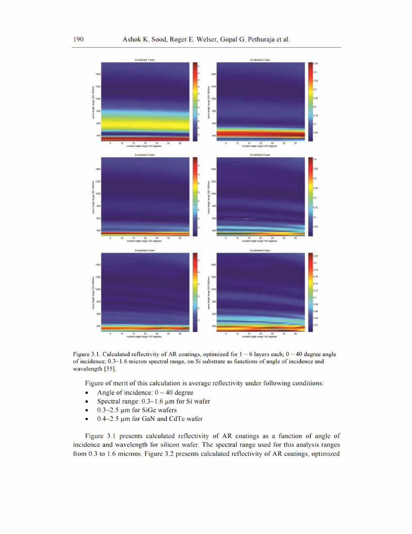
Figure 3.1. Calculated refl ectivity of AR comings, optimized for I - 6 [ayers each; 0 - 40 degree angle of incidence; 0,3- 1.6 micron speClral range, on Si substrate as functio ns of angle of incidence and wavelength l351 .
Figure or merit of this calculation is average refl ectivity under following condi tions :
• Angle of incidence: 0 - 40 degree • Spectral range : 0.3- 1.6 )J m for Si wafer • 0.3- 2.5 11m for SiGe wafers • 0.4- 2.5 11m for GaN and CdTe wafer
Figure 3.1 presents calcu lated reflectivity of A R coatings as a funct ion of angle of inc idence and wavelength fo r si licon wafer. The spectral range used for this analysis ranges from 0.3 to 1.6 microns. Figure 3.2 presents calculated reflectivity of A R coati ngs, opti mized
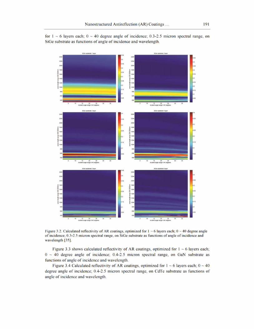
Nanostructured Antireflection (AR) Coatings . 191
for 1 - 6 layers each; 0 - 40 degree angle of incidence; 0.3-2.5 micron spectral range, on SiGe substrate as func tions of angle of incidence and wavelength .
•• • ..
•• • • •
• • ... • .. •• •
Figure 3.2. CalculaTed reflccTivity of AR coaTings, optim ized for 1 - 6 [aycrs each ; 0 - 40 degrec anglc of incidcnce; 0,3-2 .5 micron specTral range, Otl SiGc subslrate as fU tlctions of angle of incidetlce atld wavelcngth l351 .
Figure 3.3 shows calculated reflectivity of AR coatings, optimized for 1 - 6 layers each; o - 40 degree angle of incidence; 0.4-2 .5 micron spectral range, on GaN substrate as functions of angle of incidence and wavelength.
Figure 3.4 Calculated reflectivity of AR coatings, optimized for 1 - 6 layers each; 0 - 40 degree angle of inc idence; 0.4-2 .5 micron spectral range, on CdTe substrate as functions of angle of incidence and wavelength.

192 Ashok K. Sood, Roger E. Welser, Gopal G. Pethuraja et al.
o. 0-
o. "0
• " I • • t, • •
I' • • • o.
o. o.
-----o.
o. o.
o. o.
I " • • o •
r " •
I' • • " o.
o.
" o.
Figure 3.3. CalculaTed refleCTivity of AR coaTings, optim ized for I - 6 laycrs each; 0 - 40 degrec angle of incidence; 0.4-2 .5 micron specTral range, Otl GaN subsTraTe as fUtictions of anglc of incidetiCc atld wavelength l351 .
Fi gure 3.5 summarizes the calc ulated average reflectivity as a funct ion of number of layers on Si, SiGe, GaN and CdTe substrates. This analysis shows that high qual ity AR coatings can be modeled .

Nanostructured Antirenection (AR) Coatings. 193
" •• •• •• • • • • • • • • • •• • ,. •• ,. ,.
Figure 3.4. CalculaTed refleCTivity of AR coaTings, optimized for 1 - 6 layers each; 0 - 40 degree angle of incidence; 0.4-2 .5 micron specTral range, on CdTe subsTrate as funCTions of angle of incidence and wavelength l351.
4 . D ESIGN OPTIM IZATION
Optimization of multilayer antirenection coatings is difficult because of the high cost of evaluating the performance for a given structure . In addition, the parameter space generally includes many local minima, which makes deterministic optimization schemes that find the local mi nima unsuitable . To meet these challenges, genetic algorithms have previously been applied in order to optimize a variety of optical coatings . Genetic algorithms mirror biological

194 Ashok K. Sood, Roger E. Welser, Gopal G. Pethuraja et al.
evol ution in which the fi tness of a population is increased by the processes of select ion, crossover, and mutation .
In this work, we apply a genetic algorithm to optimize antireflection coatings for silicon image sensors, si licon solar cells, and triple-junction Ge/GaAs/GalnP solar cells with air as the ambient medium. The calc ulations consider coatings composed of co-sputtered and ]ow-n materials and take material dispersio n into account.
40 ,-,----,---,,---,----,----,----,-,
o
-#. 30 -
o
o
Figure of merit: - Angle of incidence: 0 - 40° - Spectral range: 0.4 - 2 . 5~tm
Layer: Ti02 or Ti02lSi02 or Si02 nanorods
-D- Si
-O-SIGe - e - GaN - . - (dTe
9 4l 8 1- , . 1 3 4
Number of layers 5 6
Figure 3.5. CalculaTed average reflectivity as a fUllClion of number of layers o n Si, SiGe, GaN and CdTc substrates l351 .
4.1. Si licon Image Sensor
Silicon image sensors are widespread in defense and commercial applications, and generally capture light in the visible wavelength range. Low reflection from the sensor surface is desi rable to increase the absorbed light and decrease the no ise in the resultant image . The reflection coeffic ient should also be low over a wide range of incident angles; depending upon lens configuration, the angle of incidence of light on the sensor surface can vary. Strong angular dependence of reflection can produce undesirable vignetting. Finally, the reflection coefficient must be cons istently low across the entire vis ible wavelength range of 400 to 700 nm.
Figure 4 .1 shows the reflection coeffic ient of bare silicon and optimized one- and threelayer antireflection coatings as a function of wavelength and inc ident angle . The reflection for bare silicon is high throughout the range of wavelengths and angles.

Nanostructured Antirenection (AR) Coatings. 195
~
~ ~
, , -- -c
'" • ~
·0 IE
01 • C 0 • 0 - c c • 0
" U ·0 • c " • a:
Wavelenglh (nm) Wavelenglh (nm) Wavelength (nm)
Figure 4. 1. Refl eelion coefficient of (left ) silicon and optim ized (center) one- and (right) three-layer ant irefleelion coatings for silicon image sensors versus wavelenglh and incident angle [35] .
The single-layer coating has a minimum near ). = 540 nm at small angles of incidence, where the renection coeffi cient is below 0.5%, and reduced renection coefficient val ues throughout the range compared to bare silicon. The three-layer coating has th ree distinct mini ma which combine to give reflection coeffic ients less than 2% for the majority of wavelengths and incident angles; for optimized antirenection coatings for the silicon image sensor, the num ber of local minima in renection is equal to the number of layers used. The layer compositions and thicknesses of these optim ized coatings are listed in Table 4.1.
Tab le 4.1. T hickn ess t (in nm) and com posit ion C o( ind ividua l laye rs (or optimized silicon image senso r antireflection coatings. (CS = co-sputtered layer. NP = nano-porous
low-Il layer)
I -layer 2-layer 3-layer 4-layer
" 68 .4 327.7 362.8 293.4
" 65 .6 91.9 115.6
" 42 .7 75 .4
41.7
" CS, 36% TiOl NP, 14% SiOl NP, 10% Sia l NP, 10% SiOz
" CS, 42% TiOl CS, 4% Ti0 2 NP, 35% SiOz
" CS, 98% TiOl CS, 15% TiOz
CS, 100% Ti0 2

196 Ashok K. Sood, Roger E. Welser, Gopal G. Pethuraja et al.
Layer th icknesses and compositions sho uld be with in several percent of the specified val ues in order to ach ieve performance si milar to the given structure. In the optimized
antirenection structures for the si licon image sensor, generally about hair of the layers are composed of nano-porous low-n Si02. The same is true for antireflection coati ngs optimized for other applications, as will be shown later. This finding underscores the importance of lown materials in achieving high performance anti reflection coatings .
The reflection coeffic ient as a function of layer number for optimized coatings is shown in Figure 4.2 . The reflection coefficient ini tially decreases rapidly as more layers are added, and then becomes almost constant.
The angle- and wavelength-averaged reflectivity of the three- and four- layer antireflection coatings are si milar at 4.4% and 3.9%, respectivel y; the top layers of the threeand four-layer ant ireflection coatings each are composed of 90% porous SiO, - which gives the lowest allowed refractive index, while the bottom layers of both coatings are pure or nearl y-pure T i0 2 - which gives the highest ach ievable refractive index.
~45 ST " ' , 0 ~ I Icon Image sensor - 40 41 c \ Angle- and wavelength-Q) \ "u 35 \ averaged reflection ~ 30
\ \
0 \
u 25 r \ 400 :s A. :s 700 nm _ c \ 0 \ 0° :s e :s 90° :;:; 20 r- \ -U .. Q)
t;:: 15 r , -Q) , ~
, 10 r
, -Q) .,
Ol
'" ,
5 r , '.----.-~
Q) >
0 ~ 0 1 2 3 4
Total number of layers
Figure 4.2. Angle- and wavelength-averaged reflect ion coefficient as a funClion of lhe number of layers for oplimized antirefleClion coatings for a silicon image sensor [35 J.
As mentioned above, the three- and four-layer coatings also have sim ilar reflection coeffic ients. This is a general characteristic for anti reflection coatings: once a sufficient number of layers is used so that the optimum stack contains layers with both the highest and lowest allowed refractive index, increasing the layer number further has onl y a small effect on the reflection coefficient.

Nanostructured Antireflection (AR) Coatings . 197
4.2. Silico n Solar Cell
The si licon solar cell is one of the most widespread technologies for photovoltaics ; the relevant spectral range for this application is 400 to 1100 nm . One or two- layer antireflection coatings and surface texturing are common methods used to reduce reflection from the surface and increase efficiency. Using the genetic algorithm approach, antireflection coatings for silicon solar cells with up to five layers are optimized .
The reflection coefficient as a function of wavelength and inc ident angle is shown in Figure 4-3 for optimized one-, two-, and four-layer antireflection coatings. As before, the number of minima in reflection is equal to the number of layers in the anti reflection coating. The compos itions of optimized coatings are shown in Table 4-2 . Agai n, nano-porous layers compose roughly halfofthe layers in an antireflection coating wi th a given number of layers.
400 600 800 1000 Wavelenglh (nm)
400 600 800 1000 Wavelength (nm)
400 600 800 1000 Wavelength (nm)
100 50 ~
* 20 :: <:
10 .~
"' 5.0 • o
2.0 u <:
10 ~ 05 ~
• 0.2 a: 0.1
Figure 4.3. RefleClion coefficient or (lef!) one-. (celller) two-. and (righl) rour- layer alllireflection coalings oplimized ror silicoll solar cells versus wavelenglh aud incidenl angle 135] .
Compared to the one- and two-layer coatings, the four-layer coating yiel ds substantially reduced reflection, particularly at the largest incident angles and shortest wavelengths. Note that the one- and two-layer coatings feature one co-sputtered layer and both nano-poro us low-n and co-sputtered layers, respectively, which wi ll give enhanced performance compared to conventional one- and two-layer coatings . The angle- and wavelength-averaged reflection.
Coefficients are plotted in Figure 4.4 as a funct ion of the number of layers. As disc ussed above, when an optimized antireflection coating includes layers with both the lowest allowed and highest allowed refractive index, adding additional layers generally prov ides little benefit.
In the case of the silicon solar cell , which is identical to the image sensor with the exception that the relevant wavelength range is broader, a larger number of layers is needed to reach this threshold .

198 Ashok K. Sood, Roger E. Welser, Gopal G. Pethuraja et a l.
Table 4.2. Thickness ' (in 11m ) and co mpos ition c of indi"idu allaycrs for optimized s il icon solar ce ll antireflection coatin gs
(CS = co-sputtered layer, NP = nano-porous low-II layer)
1. layer 2· laycr 3-laye r 4.laye r 5-laycr
" 9 1.2 133.1 432 .8 432 .6 388.7
" 64.0 1133 145.8 159.3
" 58.6 79.7 107.8
'. 51.2 70.1
" 50.5
" CS. 36% TiO, N P, 78% SiO, NP. ll % SiO, NP.1 0% 5iO, N P, 10% SiO,
" CS. 70% TiO, CS, 30/. TiO, NP, 54% SiO, NP, 29% SiO,
" CS, 82% TiO, CS, 28% TiO, N P, 81 % SiO,
" CS, 100010 TiO, CS. 37% TiO,
" CS. 10001. TiO,
~ 45 Silicon solar cell ~ - 40 c ~ Angle- and wavelength-Q)
35 \ '13 \ averaged reflection if: \ Q) 30 \ 0 \ u
25 \ 400 " A " 1100 nm c \ 0 .. 0° " e " 90° ., 20 -u , Q) ,
0= 15 ,
[i! , .,
Q) 10 , , Cl '. ~ 5 ---e---. Q) >
0 , , , «
0 1 2 3 4 5 Total number of layers
Figure 4.4 . Angle- and wavelength-averaged reflection coeffi cient as a fUllclion of the lI U111bcr of layers for oplimized antirefleelion coatings for silicon solar cells [35 J.
In the image sensor, goi ng from three to fo ur layers reduces average reflectivity by 11 . 1 %, whi le fo r the solar cell , refl ectivity is reduced by 31 . 1 %. Add ing an fi ft h layer to the
solar cell antirefl ection coating reduces reflection by an additional 5.6%. We have described a method for optimizing antireflect ion coatings made of co-sputtered
and nano-porous low-refractive-index coatings. The method is based on a genetic a lgorithm wh ich is well suited for the task of optimizing optical thin-fil m coatings, given the fact that
the design space of multi-layered optical coatings incl udes many local minima of the fitness

Nanostructured Antireflection (AR) Coatings . 199
function, i.e., the average reflectivity. The optimizat ion method was applied to si licon image sensors and solar cell s. In each case, nano-porous layers consti tute rough ly half of the total number of layers in optimized antireflection coati ngs, which underscores the importance of low-refractive-index materials for high-performance antireflection coati ngs.
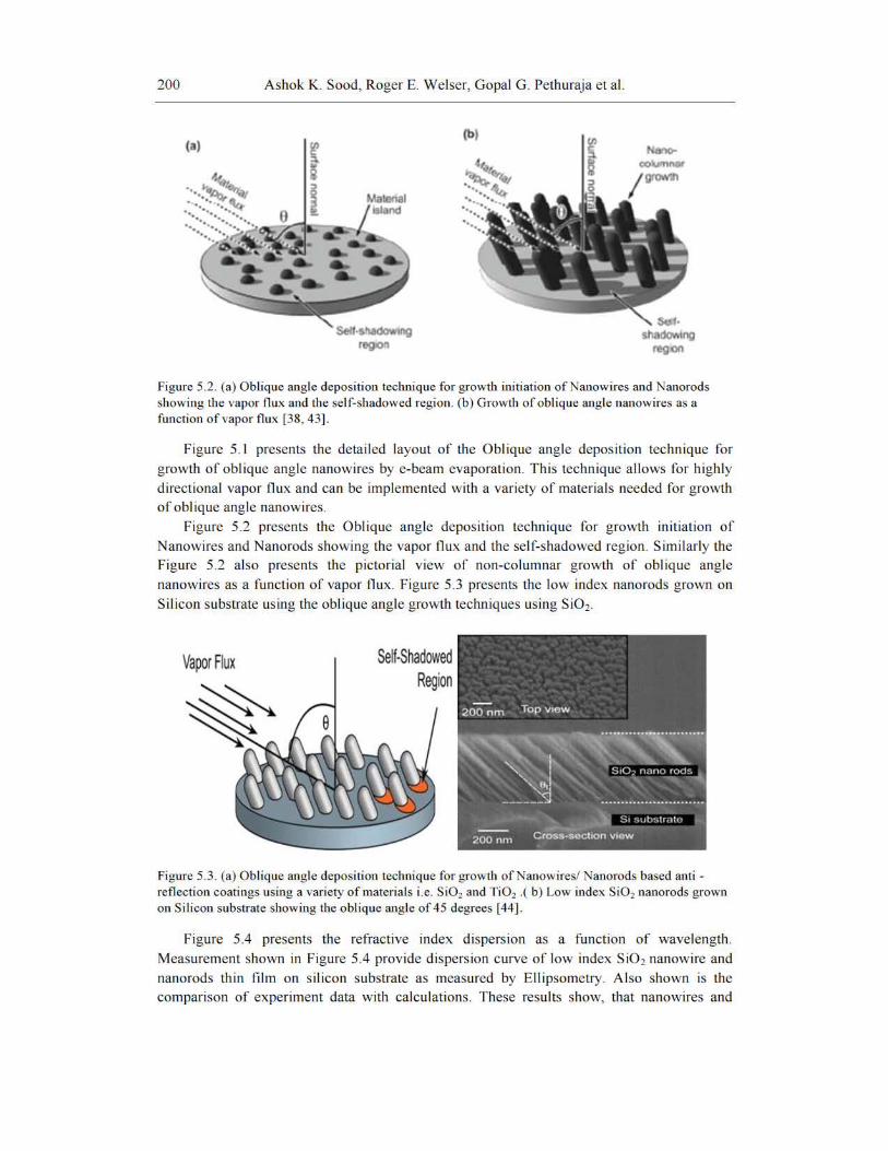
5 . C ROWTI ' AN D C II ARACTER' ZA TlO N OF O BLIQ UE
ANG LE NANOW 'RES
The use of Nanowires for developing the cri tical technologies that will allow minimizing the reflection loss has recently been studied by Schubert et a!. , at RPI [8]. Thei r work has explored the possibi lity of using nanowires grown by oblique angle deposition technique as shown in Figure 5.1. Their investigation was based on studying the work by Lord Rayleigh that graded-refracti ve index layers have broadband antireflection characteristics [8].
Graded-index coatings wi th different index profiles have been investigated for broadband antireflection properties, particularly with ai r as the ambient medi um. However, beca use of the unavailability of optical materials with very low refractive indices that closely match the refractive index of air, such high quality broadband antireflection coati ngs have not been real izable. The work carried out by Schubert et a!. , [8] uses Ti02 and Si02 graded-index nanowi res and nanorods deposited by oblique-angle deposition, and, for the firs t time, demonstrated their potential for antireflect ion coatings by virtually el imi nating Fresnel reflect ion from an AIN- air interface over the UV band. This was achieved by controll ing the refractive index of the TiO, and Si0 2 nanorod layers, down to a minim um value of n = 1.05 , the lowest value so far reported [8].
ComputorCOntrOlleo Rotating
Plate Attaches to Cei!W1g I" of Vacuum Chatrber
-~~ • . .
.'-' • 0 • • •
Sa~ Mount ;
&!mplo
/:,' .,. 1/
", . •
. • + .. .2 . ~ . •• ~ : -.
• • •
fJ CrucI>+e wi:h
SouI08 Materia!
Figure 5.1. Oblique angle deposition technique for growlh of nan ow ires I nanorods based Anti -RefleClion Coati ngs by E-beam evaporation l38. 43].
200 Ashok K. Sood, Roger E. Welser, Gopal G. Pethuraja et a1.
(hI ...... --
Figure 5.2. (a) Oblique angle deposition technique for growlh initialion of Nanowircs and Nanorods showi ng the vapor fl ux and Ihe sel f-shadowed rcgioll . (b) Growth of obl ique angle nanowires as a fu nction of vapor flux [38, 43j.
Figure 5.1 presents the detailed layout of the Oblique angle deposition techniq ue for growth of oblique angle nanowires bye-beam evaporation. Th is technique allows for highly di rectional vapor fl ux and can be implemented with a variety of materials needed for growth of oblique angle nanowi res.
Figure 5.2 presents the Obl ique angle deposition technique for growth initiat ion of Nanowi res and Nanorods showing the vapor fl ux and the self-shadowed region. Simi larly the Figure 5.2 also presents the pictorial view of non-col umnar growth of oblique angle nanowi res as a function of vapor flux. Figure 5.3 presents the low index nanorods grown on Si licon substrate using the oblique angle growth techniques using Si02.
Vapor Rux SeH-Shadowed Reg~n
Figure 5.3. (a) Oblique angle deposition technique for growlh of Nanowiresl Nanorods based anti -re fl ection coati ngs usiug a variety of materials i.c . Si02 and TiOl .( b) Low indcx Si02 nalJorods grown on Si licoll substrate showing the obliquc angle of 45 degrecs [44].
Figure 5.4 presents the refractive index dispersion as a fu nction of wavelength. Measurement shown in Figure 5.4 provide dispersion curve of low index Si0 2 nanowire and nanorods th in fi lm on si licon substrate as measured by Ell ipsometry. Also shown is the comparison of experiment data with calcu lations. These results show, that nanowi res and

Nanostructured Antireflection (AR) Coatings . 201
nanorods grown by oblique angle techniques provides a path fo r broad band high quality ant ireflection coating for variety of Nanosensor Applications .
1.057 (a)
~ , ~
c: 1.056 x III '0 c: 1.055 III .1! -0 (1)
1.054 ~ ... III II:
1.053 400
50
~ 45 ~ 0 ~
ct 40 I
Ellipsometry Model
Cauchy layer (Si02 nanD rods)
Si substrate
h = 482 nm
h
500 600 700 800 Wavelength A (nm)
Low-n Si02 nanorod film Thickness; 1346 nm Refractive index; 1.08 Substrate; Silicon
30 Measurement
25
400 500 600 700 800 900 Wavelength 1_ (nm)
Figure 5.4 . (a) Measurement of dispersion curve of low index SiOl nanorod thin film on Silicon substrate as measured by Ellipsometry. (b) comparison of experimental data with calculat ions [8 J.
202 Ashok K. Sood, Roger E. Welser, Gopal G. Pethuraja et a1.
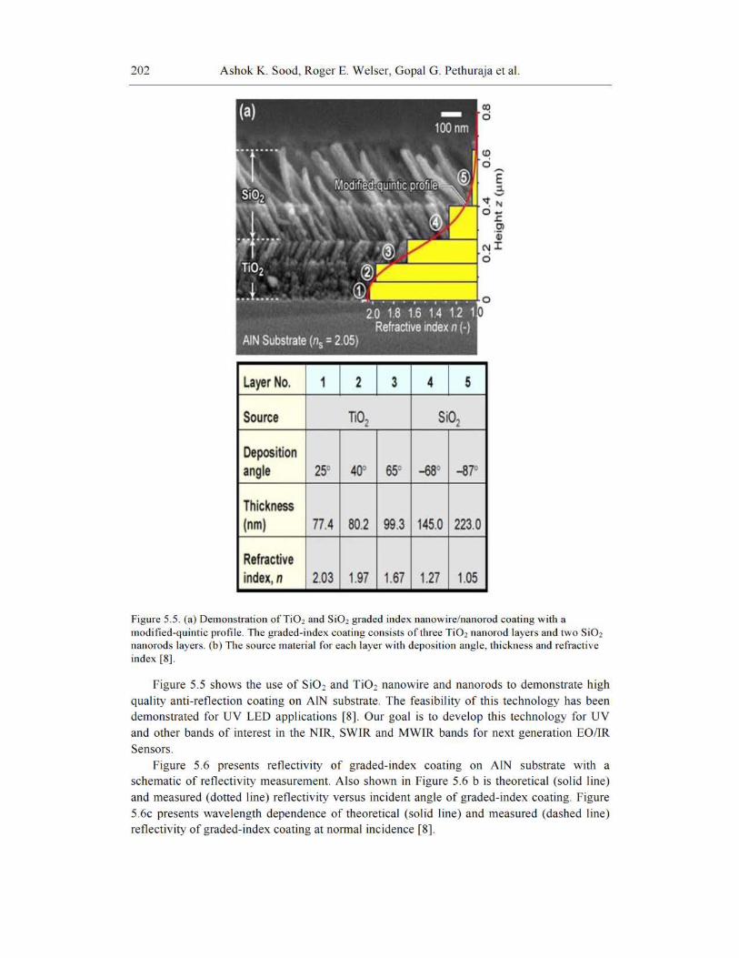
Layer No. 1 2 3 4 5
Source TiD, SiC , Deposition angle 25' 40' 65' -88' -87'
Thickness (nm) 77.4 80.2 99.3 145.0 223.0
Refractive indexl n 2.03 1.97 1.S7 1.27 1.05
Figure 5.5. (a) Demonstration of TiOl and SiOl graded index nanowire/llanoroo coating with a 1l1Odified-quintic profile. The gradcd-i ndcx coating consists ofthrec Ti02 nanorod laycrs and two SiOl nanoroos laycrs. (b) TIle sourcc matcrial for each laycr with dcposition angle. thickness and refractive index [8].
Figure 5.5 shows the use of Si0 2 and Ti02 nanowire and nanorods to demonstrate high quality anti-reflection coating on AIN substrate. The feasibi lity of this technology has been demonstrated for UV LED applications [8]. Our goal is to develop th is technology for UV and other bands of interest in the NIR, SWIR and MWIR bands for next generation EO/ IR
Sensors. Figure 5.6 presents reflectivity of graded-index coati ng on AIN substrate with a
schematic of reflectivity measurement. Also shown in Figure 5.6 b is theoretical (sol id line) and measured (dotted li ne) reflectivity vers us inc ident angle of graded-index coating . Figure 5.6c presents wavelength dependence of theoretical (solid line) and measured (dashed line) reflectivity of graded-index coati ng at normal incidence [8].

Nanostructured Antirenection (AR) Coatings .
(a) n _ 1 .0
TiO SIO g raded- index AR coating, ___ -t
A IN subs t ra te n _ 2 .05
Measure m ent
0 .10%
~-~~~~-i~~.~.-:.~. r Calculat ion
o
I). - 632.8 nml
M easurem e nt '-.
4 .. .. ..
20 40 60
Ca lc ulation
so tncident angle e ( 0 )
~ 1 00<T0>----------------~----------------,
'" '" :f ' :i 0 .1 & 0 .0 1
0 .4
~~~~~~-:-;-~.O--O·O.O-O-,. .. ""-------------Calculation
0 .6 1 .2 1 .6 2 .0 Wavelength ). (~m)
203
Figure 5.6. Refleclivity of graded-index coating on AIN substrate (a) Schematic of reflectivity mcasurement. (b) Theoretical (solid line) and measured (dotted line) re fl ectivity versus incident angle of graded-index coati ng. (c) Wavelength dependence of theoretical (solid line) and measured (dashed line) reflectivity of graded-index coating at normal incidence L8].
r- 0.1 % Reflectivi~ _________ J ______________ _
10·L..=--::::-:7-c:,-,..,....~......J 0.4 0.6 0.8 1.0 1.2 1.4 1.6 1.8
Wavelength (~m)
~ 10-2
'" :ri " :::. 10-4
'" :~ ~ 10~ &
TE polarization
TM polanzahoo
10 -''-~'''""=__='_7:,--::__c~~ ... o 10 20 30 40 50 60 70 80 90
Incident angle (degrees)
Figure 5.7. (a) Simulat ion of reflectivity as a function ofwavclength for Visible-NIR from 0.4 to 1.8 microns using oblique angle nanowires. (b) Si mulat ion ofrefleClivity as a function ofpolari7.at ion for incident angles from 0 to 90 degrees [38].

204 Ashok K. Sood, Roger E. Welser, Gopal G. Pethuraja et a1.
Figure 5.7(a) presents the simu lation of renectivity as a funct ion of wavelength from Visi ble to Near Infrared band; from 0.4 to 1.8 microns usi ng oblique angle nanowi res.
Figure 5.7 (b) demonstrates the sim ulation of renectivity as a function of polarization for inc ident angles from 0 to 90 degrees. The results show that modeli ng and simulation can be used effectively fo r developing nanowi re based high quality antirenection coating that provides coverage form UV, Visi ble and to NIR bands .
5. 1. Experimental Results
In this section, we descri be our AR coating design as a two-layer A R coating with each layer having a tailored refractive index fab ricated by using oblique angle electron -beam deposition . The appropriate depos ition angle was then chosen for the deposition of the actual A R coating layers based on Figure 5-8 and the req uired value of the refractive index [37]. Three samples were prepared: (a) a reference glass substrate with no AR coating (called Sample A), (b) a glass substrate with two-layer AR coating on one side (called Sample B), and (c) a glass substrate wi th two-layer AR coating on both sides (called Sample e).
The two-layer A R coating is composed of a 1 st layer of porous Si0 2 (P = 22%, n = 1.36 at 630 nm, t = 197 nm) deposited at 540 substrate angle, and a 2'''1 layer of porous SiO, (P =
60%, n = 1.18 at 630 nm, t = 289 nm) deposited at 780 substrate angle. The thickness and refractive index values of each coating are measured usi ng variable
angle spectroscopic ellipsometry . The thickness values were also confi rmed us ing scann ing electron microscopy. Note that all layers of the multi-layer A R coating are made of single material , porous si lica (porous SiO,) . Silica is an excellent choice as material for AR coating on glass substrate as it is native, stable, and robust.
The optical transmittance of the multi-layer AR samples was measured using (i) a normal inc idence broadband spectrophotometer measurement setup and (ii) a variable angle and wavelength dependent transmittance meas urement setup.
The thickness of the glass substrate used is 250 11m, much greater than the range of wavelengths under consideration; therefore we do not expect optical interference effects from the substrate. Figure 5.8 shows the measured wavelength dependent transmittance of glass substrate with (a) no AR coating (Sample A), (b) single-s ide two-layer AR coating (Sam ple B), and (c) double-side two-layer AR coati ng (Sample C). The inset shows the scanning electron micrograph of the two-layer AR coating.
The wavelength dependent normal incidence transmittance of Sample A, B, and C is measured between 200 nm and 2000 nm using JASeO V-570 spectrophotometer. The measurements reveal that the average transmittance between 400 nm and 2000 nm fo r uncoated glass substrate is 92.2% (Sample A) and it increases to 95 .1% for glass substrate with two-layer A R coating on one side (Sample B) and further increases to 98 .1 % fo r glass substrate with two-layer A R coating on both sides (Sam ple e). The local minima seen in the transmittance curves around 700 nm are due to the th in-film interference effects of the AR coating. The average transm ittance between 1000 nm and 2000 nm fo r glass substrate with double side AR coating is measured to be 99 .3%.
Angle dependent reflectance measurements between 350 nm and 1700 nm are performed using a custom-bui lt laboratory setup. For each sample, the reflectance data is measured for

Nanostructured Antirenection (AR) Coatings . 205
angles of incidence ranging between 00 and 800 with 5 0 increments . Figure 5.9 shows the plots of the measured angle dependent transmittance .
_ 100 >Ii!. "- 90 .... a> 80 " c
70 '" .=E E 60 ~ c jg 50
rl a 40 0 30 "0 a>
20 ~
" ~ '" 10 a> ::;;
0 0.2
Sample A : Reference
Sample B: Single-Side 2-Layer AR on "'o • .{
Sample C: Double-Side 2-Layer AR on
T measured at normal incidence
; D .1. water "ea',ne'" Lines:
0 .1. water treatment
OA 0.6 0.8 1.0 1.2 1A 1.6 1.8 2.0 Wavelength A (~lm)
Figure 5.8. Measured wavelength dependent nOnllal incidence It"ansmillance of glass substrate with (a) no AR eoating, (b) single-side two-layer AR coating. and (e) double-side two-layer AR coating. TIle inset shows the seanning electron micrograph of the two-layer AR coating L37J.
- 100
"" 0 - 90 f-Q) 80 " c ro 70 -'" E
60 '" c '" 50 ~ -ro 40 " --c. 0 30 "0 Q) 20 ~
" '" ro 10 Q)
::;; 0
0
Sample C: Double-Side 2-Layer AR on Glass ~
Sample B: Single-Side 2-Layer AR on Glass ----
Sample A : Reference Glass ----
10 20 30 40 50 Angle of Incidence 0
60 (0)
70 80
Figure 5.9. Measured angle dependent transmittance of glass substrate with (a) no A R coating, (b) single-side two-layer AR coating, and (c) double-side two-layer AR coating L37J.

206 Ashok K. Sood, Roger E. Welser, Gopal G. Pethuraja et a1.
11 shows very-high transm ittance over a wide range of incident angles, demonstrating the predicted broadband and omni-directional characteristics of the two-layer graded- index AR coating. The average transm ittance, for wavelengths between 350 nm and 1700 nm and inc ident angles between 0° and 40°, for the uncoated glass substrate is 92% (Sample A) and it increases to 94 .6% for glass substrate with two-layer A R coating on one side (Sample B) and furthe r increases to 98 .3% for glass substrate with two-layer AR coating on both sides (Sample C).
Whi le the mechanical stability of porous films can be an area of concern, we have not observed any signs of disi ntegration, degradation of performance, or other adverse effects on these samples even after several months . As a test, we immersed the three samples in an ultrasonic water bath for 15 minutes .
The samples were then blow-dried with N2 and baked at 120° e fo r 12 hours in an N2 ambient. The transm ittance of all three samples was then re-measured using the JASeO spectrophotometer; the transmittance showed no significant change at wavelengths longer than 800 nm. The adhesion of the multi-layer AR coating made from nanostructured thin fi lms was tested using a ' scotch tape test ' in which a piece of standard adhesive backed packing tape was applied to the sample and then removed. The AR coating was not damaged during the test. The measured average optical transmittance of an uncoated glass substrate between 1000 nm and 2000 nm is improved from 92.6% to 99.3% at normal inc idence by using a two-layer A R coating deposited on both surfaces of the glass substrate .
We have also fabricated and tested a number of different step-graded antireflection structures on glass substrates [8 , 14, 16, 37- 39, 44]. In particular, oblique angle deposition has been used to depos it both two- and three-layer structures comprised of nanostructured Si0 2. These multi-layer antireflect ion structures have been deposited both on one and on two sides of a glass substrate, and the transmittance characterized as a function of wavelength and inc ident angle .
Fi gure 5.10 compares the measured broadband performance of an uncoated glass slide to a glass slide coated on two sides wi th a multi-layered, nanostructured SiO, coating. The nanostructured coatings were prepared in an electron-beam evaporator using different deposition angles to form distinct layers with a step-graded refractive index profile. The inset in Figure 5. 10 shows a representati ve cross-sectional scanning electron micrograph of a twolayer structure. The transm ittance of the coated and uncoated glass slides was measured using an angle dependent transmittance measurement setup consisting ofaXenon lamp light source and an Ando AQ63 15A optical spectrum analyzer calibrated to detect transmitted photons over a broadband spectrum (400 nm - 1800 nm).
The measured peak broadband transmittance at normal inc idence of the uncoated glass slide is 92%, in-line with the expected approximate 4% reflect ion loss at each glass/ai r interface . The peak transmittance increases to 98 .3% for the double-sided, nanostructured coated glass, imply ing an average broadband reflection loss of less than 1 % at each glass/ai r interface .
As shown in Figure 5.10, the transmittance through the nanostructured SiO, coated glass is also significantly higher than the uncoated glass across a wide range of inc ident angles. While the transm ittance of the uncoated glass slide falls below 80% at an incident angle of 65", the glass slide with the double-sided coating still maintains a transm ittance above 95%.

'" u
" .. -.",
E ~
" .. t!=
Nanostructured Antirenection (AR) Coatings .
Nano structu red Coated Glass 100 t~-~-+---~~""";~~:"::':
so
" .. " " 0
Nanoporous Si0 2; n = 1.18
!J[{iII~:Pf",:.i, Nanoporous $;02; n = 1 .36 ~
200nm Substrate
10 " " "
Uncoated Glass
" " Angle of Incidence (deg)
80 90
207
Figure 5.10. Angle-of-incidcnec depcndcnt broadband transm iUance lJlcasurementthrough a glass slide coated on both sides with a step-graded. nanostrUClUred SiOz antireflection structure, Also shown is the measured broadband translllinance of an ullcoated glass slidc. and a cross-sectional scanning electron micrograph ofa two-layer nanostructured coating [38].
100
9. ~
'#. - .. '" U c: 9. m --E 9Z
'" c: 90
~ •• . 6
Nanostructu red Coated Glass
Uncoat ed Glass
I· I· . I· I· . I· . I . . I
200 400 600 800 LOOO 1200 140 0 1600 1800 2000
W ave length (nm)
Figure 5.1 I . Wavelength dependent transminance measurement of a step-graded, nanostructured SiOz antireflection coating on a glass substrate using a JASCO V-5 70 spectrophotometer [38].
The transmittance of coated and uncoated glass slides has also been measured as a function of wavelength at normal incidence using a JASeO V-570 spectrophotometer.
As seen in Figure 5.11 , the measured transmittance through a glass slide is dramat ically improved over the entire 400 nm to 1800 nm spectrum by the application of a nanostructured antirenection coating. In particular, the average meas ured broadband transm ittance between 350 nm and 1800 nm increases from 92.2% for the uncoated glass, to 98 .6% for the double-

208 Ashok K. Sood, Roger E. Welser, Gopal G. Pethuraja et a1.
sided, nanostructured coated glass . Moreover, the transmittance through the glass coated with a nanostructured Si0 2 coating exceeds 97 .8% at all wavelengths between and 440 nm and
1800 nm, implying a glass-ai r interface reflecti vity below 1.1 % over a wide range of wavelengths. Optimized nanostructured antireflection coatings have been shown to outperform an ideal quarter-wavelength Mg F2 coati ng over all wavelengths and incident angles [ 14].
We have demonstrated a multi-layer, broadband, Omni -directional AR coating made ofa single material wi th tai lored -refractive-index layers on a glass substrate . The availability of the nanostructured low- and tunable-n materials deposited by using obl ique-angle deposition has allowed the fabrication of highly effective A R coatings fo r low index substrates such as glass .
6 . GRown, OF L AB-SCALE NANOW'R E AR C OATING
Nanowire AR layers are grown in an electron-beam evaporation system. A fixtu re modification on the evaporation system allowed demonstrating potential growth on a 3-inch wafer. Figure 6.1 presents the overview of the oblique angle nanowire growth system. The
sample is kept at an obl ique angle and the cruc ible that contains the source material or multiple crucibles containing Si0 2 or Ti01 .
Figure 6.1. 111in Film and Oblique angle Nanowi rc growth Facility.

Nanostructured Antireflection (AR) Coatings . 209
Fi gure 6.2 shows the inside view of growth chamber that shows how the sam ple holder is configured in the growth chamber and the crucible location for the growth of obl ique angle nanowi re grO\vth. We designed a fixture modification that will al low us to demonstrate potential grO\vth on a 3-inch wafer. Figure 6.2, 6.3 and 6.4 shows the details of the sample holder that is used for growth of oblique angle nanowires. We designed a fixture modification that allowed us to demonstrate potential growth on a 3-inch wafer. Figure 6.5 is an optical photograph of a 3- inch AR-coated glass sample. The substrate is 3-inch diameter N-B K7 glass, a common optical glass used for high-quality optical components. The AR coating consists ofa 2-layer step-graded structure ofnanostructured SiOl, similar in design to the one described in Reference [37]. Modified sample mounting procedures were employed to accommodate the larger (and heavier) substrate during the oblique angle deposition .
Figure 6.2. Inside view of the Oblique Angle NanOSlrueture AR Coating Chamber.
Figure 6.3. Enlarged view of the NanostruClUre AR Coating sample holder.

210 Ashok K. Sood, Roger E. Welser, Gopal G. Pethuraja et al.
Figurc 6.4. Clcancd samplc holdcr and loading ofthc sample for nanOSlruCiUrc AR - Coaling fabrication .
Figurc 6.5. Optical photograph ofa nanostructurcd antircflCClion coaling on a 3-inch glass substratc .
7. LARGE AREA AR COATING D EVELOPM ENT
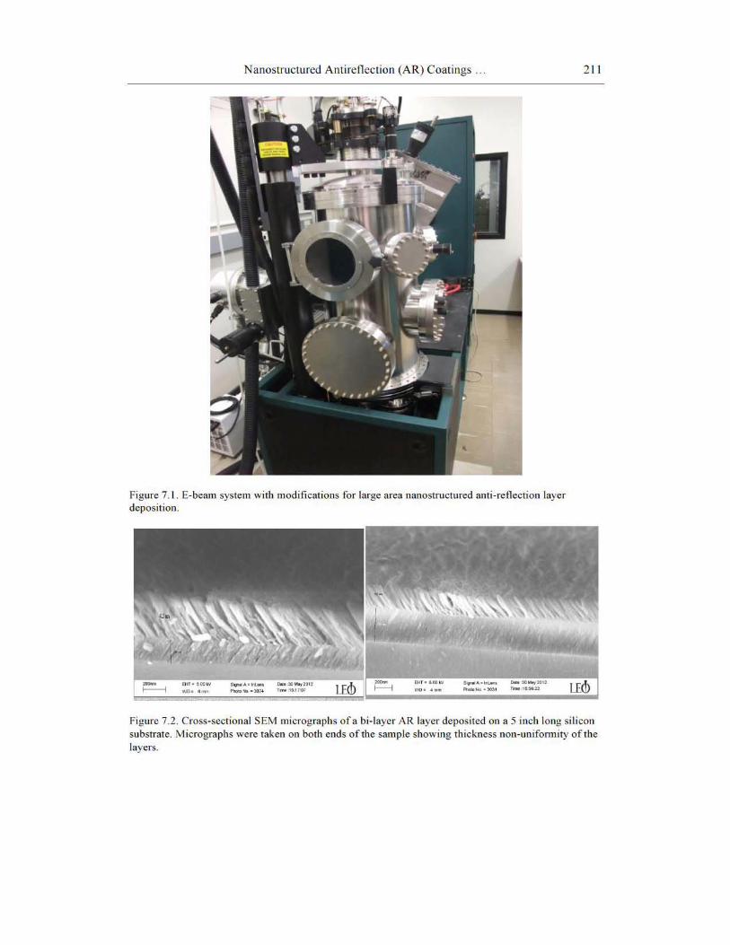
Large area A R coating has been demonstrated on a 6 inch diameter large substrate, using a larger e-beam evaporation system with high power e-beam gun and thickness monitor. Necessary modifications were made in this system to grow large area AR layers. Figure 7.1 shows the photograph of the electron-beam system used for the grmvth of large area AR coatings.
Nanostructured AR coatings deposited using the large area AR layer deposition system has the nanostructures similar to the lab-scale samples. Figure 7.2 shows the cross-sectional micrographs of a bi-Iayer AR layer structure deposited using the large area AR-layer deposition system.
The micrographs in Figure 7.2 show the layers of slanted nano-columns similar to the layer structure observed on lab-scale AR coating. It also demonstrates the controllability of the layer porosity. The bottom layer was grown at a substrate tilt of 54 degree and the top layer was grown at 78 degree resulting two different porosities in these layers.
Figure 7.3 and 7.4 demonstrate grmvth of oblique angle nanowire A R coatings on 6-inch glass and si licon substrates. The results show that the new larger system is capable of fabricating the nanostructure AR coating on 6-inch substrates. These samples will be characterized in detail and the results will be discussed in future publications.
Nanostructured Antirenection (AR) Coatings .
Figure 7.1. E-beam system with modifications for large area nanostructured anti-reflcction layer depositioll .
211
Figure 7.2. Cross-sectional SEM micrographs of a bi-layer AR layer deposited on a 5 illch long si licon substrate. Micrographs were taken Otl both ends of the sample showing thickness non-utl ifo nllity of the layers.

212 Ashok K. Sood, Roger E. Welser, Gopal G. Pethuraja et al.
Figure 7.3. Optical photograph ofa nanostructurcd antircflcction coating on a 6-inch glass substratc .
b . -'"
" .. , , ~,.I...- .... -:" e ,", .... e
Figurc 7.4. Optical photograph of a nanostructurcd antircflcction coating on a 6-inch si licon substrate.
A CKNOW LEDGM ENTS
We would also like to acknowledge the support of DARPA for development of the nanostructured AR coating for UV, Visible and IR sensor applications. We would like to
acknowledge the support of NYSERDA and the A ir Force for its applications for solar cells.
R EFE RENCES
[I] A. K. Sood, R. A. Richwine, Y. R. Puri , S. Horn, and R. S. Balcerak, " Design considerations using APD detectors for high resolution UV imagi ng applications," in Proceedings ofrhe SPIE - 71le Inrernarional Sociery for Oplical Engineering, 2009, vol. 7419, p, (8 pp.),

Nanostructured Antireflection (AR) Coatings . 213
[2] A. K. Sood, R. A. Richwine, Y. R. Puri, N. Dil ello, J. L. Hoyt, T. l. Akinwande, S. Horn, R. S. Balcerak , G. Bu lman, R. Venkatasubramanian, A. l. D' Souza, and T. G. Bramhall, " Development of low dark current SiGe-detector arrays for visi ble-N IR imaging sensor," in Proceedings of rhe SPiE - The Inremarional Sociery for Oprical Engineering, 2009, vol . 7298 , p. 72983D-72983D- I I.
[3] M. Davis, J. W. Devitt, M. E. Greiner, R. Rawe, A. Timl in, and D. R. Wade, "Advanced FPA techno logy development at CMC Electronics," in Proceedings ofrhe SPiE - The Inremarional Society for Oprical Engineering, 2004, vol. 5563, pp. 62- 73.
[4] A. K. Sood, R. Richwine, Y. R. Puri, N. K. Dhar, D. L. Polla, and p. S. Wijewarnasuriya, " Multispectral EO/1R sensor model for eval uating UV, visible, SW IR, MW IR and l WIR system performance," in Proceedings of the SPIE - The Inremational Society for Optical Engineering, 2009, vol. 7300, p. 73000H- 73000H- 12.
[5] P. W. Norton, M. Kohin, M. Dovidio, and B. S. Backer, "Commercialization of uncooled infrared technology," in Proceedings of the SPIE - The InrenJarional Sociery for Oprical Engineering, 2004, vol . 5563, no. I , pp. 55-61 .
[6] A. K. Sood, R. A. Richwine, Y. R. Puri, D. L. Poll a, N. K. Dhar, Z. L. Wang, J. M. Xu, P. S. Wijewarnasuriya, N. Goldsman, M. B. Soprano, and B. lineberry, " EOII R sensors development us ing zi nc oxide and carbon nanostructures," in Proceedings of rhe SPlE The Inremarional Sociery for Oprical Engineering, 2009, vol. 73 18, p. 73 1804.
[7] A. K. Sood, Y. R. Puri, L. Becker, M. Z. Tidrow, R. S. Balcerak , G. Brill, P. Wijewarnasuriya, N. Dhar, P. Boieriu, C. Fu lk, S. Sivananthan, J. Yehoda, and S. Finke, " Development of high-performance radiation-hardened antireflection coatings for LWIR and multicolor IR focal plane arrays," in Proceedings of rhe SPI£ - The Inremational Society for Optical Engineering, 2006, vol. 6206, pp. 620613-6206 15.
[8] XiJ .-Q., M. F. Schubert, J. K. Kim, E. F. Schubert, M. Chen, S.-Y. lin, LiuW., and S. A., "Optical thin-film materials with low refractive index for broadband elimination of Fresnel reflection," Nat Phor., vol. I, no . 3, pp . 176-179, Mar. 2007.
[9] J. Zhao and M. A. Green, "Optimized antireflection coatings for high-efficiency si licon solar cells," Electron Devices. IEEE Transactions on, vol. 38, no . 8. pp. 1925- 1934, 1991.
[10] R. G. Schuhmann and M. Schulz-Grosser, "Multiglass AR coatings in lens designs," 1997, vol. 3133, pp. 256-262.
[II] D. J. Aiken, "High performance anti-reflection coatings for broadband mu lti-junction solar cell s," Sol. Energy Marer. Sol. Cells , vol. 64, no . 4, pp . 393-404, Nov . 2000.
[12] B. Kumar, T. Baskara Pandian, E. Sreeki ran, and S. Narayanan, "Benefit of dual layer si licon nitride anti-reflection coating," PholOl'olraic Specialists Conference. 2005. Conference Record of the Thirty-/irstIEEE. pp. 1205- 1208, 2005.
[13] D. J. Poxson, F. W. Mont, M. F. Schubert, J. K. Kim, and E. F. Schubert, "Quantification of porosity and deposition rate of nanoporous films grown by obliqueangle deposi tion," Appl. Phys. Lell. , vol. 93 , no . 10, p. 101914, 2008.
[14] R. E. Wel ser, A. W. Sood, G. G. Pethuraja, A. K. Sood, X. Van, D. J. Poxson, J . Cho, E. Fred Schubert, and J. L. Harvey, "Broadband nanostructured antireflection coati ng on glass for photovoltaic applications," PholOvolraic Specialists Conference (PVSC). 201 2 38rh IEEE. pp. 3339-3342, 2012.
[15] G. G. Pethuraja, A. Sood, R. Wel ser, A. K. Sood, H. Efstathiadis, p. Haldar, and J. L.
Harvey, " l arge-area nanostructured self-assembled antireflection coatings for

214 Ashok K. Sood, Roger E. Welser, Gopal G. Pethuraja et al.
photovoltaic devices," PholOl'oltaic Specialists Conference (PVSC). 20/3 IEEE 39th. pp. 99-102 , 2013.
[16] R. E. Welser, A. W. Sood, A. K. Sood, D. J. Poxson, S. Chhajed, J. Cho, E. F. Schubert, D. L. Polla, and N. K. Dhar, " Ultra-h igh transmittance through nanostructure-coated glass for solar cell applications," 2011 , vol. 8035, p. 80350X- 80350X- 7.
[17] Y. Ono, Y. Ki mura, Y. Ohta, and N. Nishida, "Anti reflection effect in ultrahigh spatial frequency holograph ic relief gratings.," Appl. Opt., vol. 26, no . 6, pp. 1142- 6, Mar. 1987.
[18] C. -H. Sun , A. Gonzalez, N. C. Linn, P. Jiang, and B. Jiang, "Templated biomimetic mu lt ifunctional coatings," Appl. Phys. Left., vol. 92, no . 5, p. 051 107, 2008.
[19] P. B. CLAPH AM and M. C. HUT LEY, " Reduction of Lens Reflexion by the ' Moth Eye' Princi ple," Nature, vol. 244, no . 541 4, pp. 28 1-282 , Aug. 1973 .
[20] A. Gombert, W. Gla ubitt, K. Rose, J . Dreibholz, B. Blasi, A. Heinzel, D. Sporn, W. 0 1'111 , and V. Wittwer, "Subwavelength-structured anti reflective surfaces on glass," 7hin Solid Films, vol. 351 , no . 1- 2, pp. 73- 78, Aug. 1999.
[21] Y. H. Kang, S. S. Oh, Y.-S. Kim, and C.-G. Cho i, " Fabrication of anti reflection nanostructures by hybrid nano-pattern ing li thography," Microelec,ron. Eng. , vol. 87, no. 2, pp. 125- 128, Feb. 2010.
[22] H. Deniz, T. Kh udiyev, F. Buyukserin, and M. Bayindi r, " Room temperature large-area nanoim printing for broadband biomimetic antire fl ect ion surfaces," Appl. Phys. Left. ,
vol. 99, no. 18, p. 183 107, 2011. [23] J. K. Kim, S.-J. Park, S. Ki m, H.-H. Park, K. Kim, J.-H. Choi, J. Lee, D.-G . Choi, K. Y.
Suh, and J.-H. Jeong, " Fabrication of Zr02 nanopatterns for bi omi metic anti reflection by thermal nano imprint lithography," Microelectron. Eng. , vol. 100, pp. 12-1 5, Dec . 2012.
[24] S.-H. Jeong, J.-K. Kim, B.-S . Kim, S.-H. Shim, and B.-T. Lee, "Characterization of SiO, and TiO, fil ms prepared usi ng rf magnetron sputtering and their application to anti-reflection coating," Vacuum , vol. 76, no . 4, pp. 507- 515, Nov. 2004.
[2;] R. Pmdo, G. Beob;de, A . Ma<ca;de, J. Go;koetxea, and A . Man,.be, " Development of mu ltifunctional sol- gel coatings: Anti-reflection coati ngs with enhanced self-cleani ng capacity," Sol. Energy Maler. Sol. Cells , vol. 94, no. 6, pp. 1081 -1 088, Jun. 20 10.
[26] H. Nagel, A. Metz, and R. Hezel, " Porous Si0 2 films prepared by remote plasmaenhanced chemical vapo ur deposition - a novel anti reflection coating technology for photovoltaic modu les," Sol. Energy Mater. Sol. Cells , vol. 65, no . 1-4, pp. 7 1-77, Jan. 2001 .
[27] S. Wal heim, E. Schaffer, J. Mlynek, and U. Steiner, " Nanophase-Separated Polymer Films as High- Performance Anti reflection Coatings," Sci .. vol. 283 , no . 5401 , pp. 520-522, Jan . 1999.
[28] H. Jiang, K. Yu, and Y. Wang, "Antireflective structures via spin casting of polymer latex," 0pl. Left., vol. 32, no . 5, p. 575, 2007.
[29] H. Selhofe r, E. Ri tter, and R. Linsbod, " Properties of Titani um Dioxide Films Prepared by Reactive Electron-Beam Evaporation from Various Starting Materials," Appl. Opt.,
vol. 41 , no. 4, p. 756, Feb. 2002. [30] Y. Zhao, J. Wang, and G. Mao, "Col loidal subwavelength nanostructures for
anti reflection optical coatings," Opt. Left. , vol. 30, no. 14, p. 1885, Jul. 2005.

Nanostructured Antireflection (AR) Coatings . 215
[31] M. Kursawe, R. Anselmann, V. Hilari us, and G. PfatT, " Nano-Particles by Wet Chemical Processing in Commerc ial Applications," J. Sol-Gel Sci. Technol., vol. 33, no. I, pp. 71 - 74 , 2005.
[32] B.-T. Liu and W.-D. Yeh, "Antireflective surface fabricated from collo idal si lica nanoparticles," Colloids Surfaces A Physicochem. Eng. Asp., vol. 356, no . 1- 3, pp. 145-149, Mar. 2010.
[33] A. V Tikhonravov, M. K. Trubetskov, and G. W. Debell , "Application of the needle optimization technique to the design of optical coatings .," Appl. apr., vol. 35, no . 28, pp. 5493- 508, Oct. 1996.
[34] Y.-Y. L. and C-C L. and c.-C K. and W.-c. L. and C-c. Jaing, " Design of Universal Broadband Visible Anti reflection Coating for Commonly Used Glass Substrates," Jpn.
J. Appl. Phys., vol. 46, no . 8R, p. 5143, 2007. [3;] M. F. Sch"ben, F. W. Moot, S. e hh'jed, D. J. I'oxson, J. K. Kim, and E. F. Sch"ben,
" Design of multilayer anti reflection coatings made from co-sputtered and lowrefractive-i ndex materials by genetic algori thm," apr. /:"xpress , vol. 16, no . 8, p. 5290, Apr. 2008.
[36] N. Yamaguchi, K. Tadanaga, A. Matsuda, T. Minami, and M. Tatsumisago, "AntiReflective Coatings of Flowerlike Alumi na on Various Glass Substrates by the Sol- Gel Process with the Hot Water Treatment," J. Sol-Gel Sci. Technol. , vol. 33, no . I, pp . 117- 120, 2005.
[37] S. Chhajed, D. J. Poxson, X. Yan, J. Cho, E. F. Schubert, R. E. Welser, A. K. Sood, and J. K. Kim, "Nanostructured Multilayer Tailored-Refractive- Index Antireflection Coating for Glass with Broadband and Omnid irectional Characteristics," Applied
Physics t..Xpress , vol. 4, no. 5. p. 052503 , 201 1. [38] A. K. Sood, A. W. Sood, R. E. Welser, G. G. Pethuraja, Y. R. Puri, X. Yan, D. J.
Poxson, J. Cho, E. F. Schubert, N. K. Dhar, D. L. Poll a, P. Haldar, and J. L. Harvey, " Development of Nanostructured Antireflection Coatings for EO/IR Sensor and Solar Cell Applications," Marer. Sci. Appl. va - 03, no . 09, p. 633 , 20 12.
[39] M. F. Schubert, D. J. Poxson, F. W. Mont, J. K. Kim, and E. F. Schubert, " Performance of Antireflection Coatings Consisting of Multiple Discrete Layers and Comparison with Continuously Graded Antireflection Coatings," Appl. Phys. !:.xpress, vol. 3, no . 8, p. 082502 , Aug. 20 I O.
[40] D. J. Poxson, M. F. Schubert, F. W. Mont, E. F. Schubert, and J. K. Kim, " Broadband omnidirectional antireflection coatings optimized by genetic algorithm.," apr. Lerr., vol. 34, no . 6, p. 728 , Mar. 2009.
[41] S. Chhajed, M. F. Schubert, J. K. Kim, and E. F. Schubert, "Nanostructured multilayer graded-index antireflection coating for Si solar cells with broadband and omnidirectional characteristics .," Appl. Phys. Leu. , vol. 93 , no . 25 , p. 251108, Dec . 2008.
[42] M. Born and E. Wolf, Principles of oprics: elecrromagnelic Iheor}' of propagalion. interference. and diffracrion of lighl l by Max Born and Emil Wolf wilh cOnlriburions by A. B. Bhalia ... reI al.]. Oxford , New York . Pergamon Press, 1980., 1980.
[43] A. W. Sood, D. J . Poxson, F. W. Mont, S. Chhajed, J. Cho, E. F. Schubert, R. E. Welser, N. K. Dhar, and A. K. Sood, " Experimental and Theoretical Study of the Optical and Electrical Properties of Nanostructured Indium Tin Oxide Fabricated by Oblique-Angle Deposition," J. Nanosci. Nanoledmol. , vol. 12, no . 5, pp. 3950-3953 .

216 Ashok K. Sood, Roger E. Welser, Gopal G. Pethuraja et al.
[44] D. J. Poxson, M.-L. Kuo, F. W. Mont, Y.-S . Kim, X. Yan, R. E. Welser, A. K. Sood, J.
Cho, S.-Y. Lin, and E. F. Schubert, " High-performance antireflection coatings utilizing nanoporous layers," MRS 81111., vol . 36, no . 06, pp . 434- 438, 20 11.